WO2012001939A1 - Dispositif d'imagerie à semi-conducteurs - Google Patents
Dispositif d'imagerie à semi-conducteurs Download PDFInfo
- Publication number
- WO2012001939A1 WO2012001939A1 PCT/JP2011/003643 JP2011003643W WO2012001939A1 WO 2012001939 A1 WO2012001939 A1 WO 2012001939A1 JP 2011003643 W JP2011003643 W JP 2011003643W WO 2012001939 A1 WO2012001939 A1 WO 2012001939A1
- Authority
- WO
- WIPO (PCT)
- Prior art keywords
- pixel
- transistor
- disposed
- wells
- conductivity type
- Prior art date
Links
- 238000003384 imaging method Methods 0.000 title claims abstract description 28
- 230000003321 amplification Effects 0.000 claims abstract description 85
- 238000003199 nucleic acid amplification method Methods 0.000 claims abstract description 85
- 239000000758 substrate Substances 0.000 claims abstract description 62
- 238000006243 chemical reaction Methods 0.000 claims abstract description 41
- 239000004065 semiconductor Substances 0.000 claims description 26
- 239000011159 matrix material Substances 0.000 claims description 5
- 230000002093 peripheral effect Effects 0.000 abstract description 14
- 238000000926 separation method Methods 0.000 abstract description 7
- 230000003247 decreasing effect Effects 0.000 description 6
- 230000000694 effects Effects 0.000 description 6
- 230000008901 benefit Effects 0.000 description 4
- 230000008859 change Effects 0.000 description 4
- 229910044991 metal oxide Inorganic materials 0.000 description 3
- 150000004706 metal oxides Chemical class 0.000 description 3
- 230000003071 parasitic effect Effects 0.000 description 3
- 229910021420 polycrystalline silicon Inorganic materials 0.000 description 3
- 229920005591 polysilicon Polymers 0.000 description 3
- 101100270422 Rattus norvegicus Arhgef7 gene Proteins 0.000 description 2
- 238000010586 diagram Methods 0.000 description 2
- 239000012535 impurity Substances 0.000 description 2
- 238000012986 modification Methods 0.000 description 2
- 230000004048 modification Effects 0.000 description 2
- 230000001629 suppression Effects 0.000 description 2
- 238000009792 diffusion process Methods 0.000 description 1
- 230000005669 field effect Effects 0.000 description 1
- 230000006872 improvement Effects 0.000 description 1
- 238000009413 insulation Methods 0.000 description 1
- 229920006395 saturated elastomer Polymers 0.000 description 1
- 230000035945 sensitivity Effects 0.000 description 1
Images


Classifications
-
- H—ELECTRICITY
- H01—ELECTRIC ELEMENTS
- H01L—SEMICONDUCTOR DEVICES NOT COVERED BY CLASS H10
- H01L27/00—Devices consisting of a plurality of semiconductor or other solid-state components formed in or on a common substrate
- H01L27/14—Devices consisting of a plurality of semiconductor or other solid-state components formed in or on a common substrate including semiconductor components sensitive to infrared radiation, light, electromagnetic radiation of shorter wavelength or corpuscular radiation and specially adapted either for the conversion of the energy of such radiation into electrical energy or for the control of electrical energy by such radiation
- H01L27/144—Devices controlled by radiation
- H01L27/146—Imager structures
- H01L27/14643—Photodiode arrays; MOS imagers
-
- H—ELECTRICITY
- H01—ELECTRIC ELEMENTS
- H01L—SEMICONDUCTOR DEVICES NOT COVERED BY CLASS H10
- H01L27/00—Devices consisting of a plurality of semiconductor or other solid-state components formed in or on a common substrate
- H01L27/14—Devices consisting of a plurality of semiconductor or other solid-state components formed in or on a common substrate including semiconductor components sensitive to infrared radiation, light, electromagnetic radiation of shorter wavelength or corpuscular radiation and specially adapted either for the conversion of the energy of such radiation into electrical energy or for the control of electrical energy by such radiation
- H01L27/144—Devices controlled by radiation
- H01L27/146—Imager structures
- H01L27/14601—Structural or functional details thereof
- H01L27/14609—Pixel-elements with integrated switching, control, storage or amplification elements
-
- H—ELECTRICITY
- H01—ELECTRIC ELEMENTS
- H01L—SEMICONDUCTOR DEVICES NOT COVERED BY CLASS H10
- H01L27/00—Devices consisting of a plurality of semiconductor or other solid-state components formed in or on a common substrate
- H01L27/14—Devices consisting of a plurality of semiconductor or other solid-state components formed in or on a common substrate including semiconductor components sensitive to infrared radiation, light, electromagnetic radiation of shorter wavelength or corpuscular radiation and specially adapted either for the conversion of the energy of such radiation into electrical energy or for the control of electrical energy by such radiation
- H01L27/144—Devices controlled by radiation
- H01L27/146—Imager structures
- H01L27/14601—Structural or functional details thereof
- H01L27/14632—Wafer-level processed structures
-
- H—ELECTRICITY
- H01—ELECTRIC ELEMENTS
- H01L—SEMICONDUCTOR DEVICES NOT COVERED BY CLASS H10
- H01L27/00—Devices consisting of a plurality of semiconductor or other solid-state components formed in or on a common substrate
- H01L27/14—Devices consisting of a plurality of semiconductor or other solid-state components formed in or on a common substrate including semiconductor components sensitive to infrared radiation, light, electromagnetic radiation of shorter wavelength or corpuscular radiation and specially adapted either for the conversion of the energy of such radiation into electrical energy or for the control of electrical energy by such radiation
- H01L27/144—Devices controlled by radiation
- H01L27/146—Imager structures
- H01L27/14601—Structural or functional details thereof
- H01L27/14634—Assemblies, i.e. Hybrid structures
-
- H—ELECTRICITY
- H01—ELECTRIC ELEMENTS
- H01L—SEMICONDUCTOR DEVICES NOT COVERED BY CLASS H10
- H01L27/00—Devices consisting of a plurality of semiconductor or other solid-state components formed in or on a common substrate
- H01L27/14—Devices consisting of a plurality of semiconductor or other solid-state components formed in or on a common substrate including semiconductor components sensitive to infrared radiation, light, electromagnetic radiation of shorter wavelength or corpuscular radiation and specially adapted either for the conversion of the energy of such radiation into electrical energy or for the control of electrical energy by such radiation
- H01L27/144—Devices controlled by radiation
- H01L27/146—Imager structures
- H01L27/14601—Structural or functional details thereof
- H01L27/1464—Back illuminated imager structures
-
- H—ELECTRICITY
- H01—ELECTRIC ELEMENTS
- H01L—SEMICONDUCTOR DEVICES NOT COVERED BY CLASS H10
- H01L27/00—Devices consisting of a plurality of semiconductor or other solid-state components formed in or on a common substrate
- H01L27/14—Devices consisting of a plurality of semiconductor or other solid-state components formed in or on a common substrate including semiconductor components sensitive to infrared radiation, light, electromagnetic radiation of shorter wavelength or corpuscular radiation and specially adapted either for the conversion of the energy of such radiation into electrical energy or for the control of electrical energy by such radiation
- H01L27/144—Devices controlled by radiation
- H01L27/146—Imager structures
- H01L27/14601—Structural or functional details thereof
- H01L27/14636—Interconnect structures
Definitions
- the present invention relates to a solid-state imaging device.
- a solid-state imaging device in which a photoelectric conversion unit and a part of a peripheral circuit unit or a pixel circuit are separately formed on separate substrates and electrically connected to each other.
- a light sensitive pixel and a through wiring are disposed on a first substrate and a readout circuit is disposed on a second substrate.
- the readout circuit reads out an electric signal via the through wiring and then outputs the electric signal as an image signal.
- another surface of the first substrate and the readout circuit on the second substrate are disposed to face each other, and terminals of the through wiring and the readout circuit are electrically connected to each other.
- the photoelectric conversion unit and the pixel circuit are disposed monolithically on the first substrate, and wells included in the photoelectric conversion unit are separated for each pixel.
- the photoelectric conversion unit and the pixel circuit are disposed monolithically on the first substrate, and the well of a transistor for an amplifier is electrically separated from wells of other transistors included in the pixel.
- the PTL 2 in view of influence from charge leaked from the saturated pixel, the wells included in the photoelectric conversion unit are separated for each pixel. Thus, the PTL 2 describes nothing about the separation of the wells on the substrate on which the photoelectric conversion unit is not disposed when the separated substrates are adopted.
- the well for the transistor amplifier is separated from the wells of other transistors included in the same pixel.
- the PTL 3 discusses nothing about the wells of the transistor for the amplifier included in other pixels.
- a common problem between the PTL 2 and 3 is that, since the photoelectric conversion unit and the pixel circuit are disposed monolithically on the first substrate, an extra space is needed to separate the wells, thus reducing a light receiving area of the photoelectric conversion unit.
- the present invention is directed to a preferable separation structure of wells when a photoelectric conversion unit and a part of a peripheral circuit unit or a pixel circuit are separately formed on separate substrates and electrically connected to each other.
- the present invention includes: a plurality of pixels including a photoelectric conversion unit and a transistor amplifier configured to amplify a signal generated by the photoelectric conversion unit; a first substrate on which a plurality of the photoelectric conversion units are disposed; and a second substrate on which a plurality of the transistor amplifiers are disposed.
- a well of a first conductivity type provided with a source region and a drain region of the transistor amplifier is separated from a well, which is disposed adjacent to the well in at least one direction, of the first conductivity type provided with the source region and the drain region of the transistor amplifier.
- a preferable separation structure of a well can be provided when a photoelectric conversion unit and a part of a peripheral circuit unit or a pixel circuit are separately formed on separate substrates and electrically connected to each other.
- Fig. 1A is an example illustrating an equivalent circuit of a pixel according to the present invention.
- Fig. 1B is an example illustrating an equivalent circuit of a pixel according to the present invention.
- Fig. 2 is a schematic cross-sectional view illustrating a solid-state imaging device according to the present invention.
- Fig. 3 is a schematic top plan view illustrating a solid-state imaging device according to a first exemplary embodiment.
- Fig. 4 illustrates an example of an equivalent circuit of a pixel in a solid-state imaging device according to the first exemplary embodiment.
- Fig. 5 is a schematic top plan view of one pixel in a solid-state imaging device according to the first exemplary embodiment.
- Fig. 6 illustrates an equivalent circuit of a source follower circuit.
- Fig. 1A is an example illustrating an equivalent circuit of a pixel according to the present invention.
- Fig. 1B is an example illustrating an equivalent circuit of a pixel according to the present invention.
- FIG. 7 illustrates an equivalent circuit of an extracted part of a pixel.
- Fig. 8 is a schematic top plan view illustrating a solid-state imaging device according to a second exemplary embodiment.
- Fig. 9 is a schematic top plan view illustrating a solid-state imaging device according to a third exemplary embodiment.
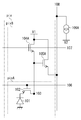
- Figs. 1A and 1B are examples of an equivalent circuit of one pixel included in a solid-state imaging device that can be applied to the present exemplary embodiment.
- a pixel is illustrated, however, actually a plurality of pixels are disposed to configure a pixel arrangement.
- a photoelectric conversion unit 101 generates holes and electrons by photoelectric conversion using, for example, a photodiode.
- a transfer unit 102 transfers charge of the photoelectric conversion unit 101 using, for example, a metal oxide semiconductor (MOS) transistor (transfer transistor).
- MOS metal oxide semiconductor
- the transfer unit 102 transfers to a floating diffusion (FD) 103 the charge of the photoelectric conversion unit 101, of which potential is in a floating state.
- FD floating diffusion
- a pixel reset unit 104 sets at least the potential of the FD 103 to a reference potential. In other words, the pixel reset unit 104 resets the voltage of an input node of a transistor amplifier. Alternatively, the pixel reset unit 104 is turned on simultaneously with the transfer unit 102 to set the potential of the photoelectric conversion unit 101 to the reference potential. As the pixel reset unit 104, for example, a MOS transistor (reset transistor) is used.
- a pixel amplifier 105 amplifies a signal based on either of paired charge generated in the photoelectric conversion unit 101 and outputs the signal using, for example, the MOS transistor.
- a gate of the MOS transistor (amplification transistor) of a pixel amplifier is electrically connected to the FD 103.
- a transfer control line 106 is used to control an operation of the transfer transistor.
- a reset control line 107 is used to control an operation of the reset transistor.
- a driving pulse is supplied from a vertical scanning circuit (not illustrated) to the control lines described above.
- Signals amplified by a plurality of pixel amplifiers included in a pixel column are sequentially output to a vertical output line 108.
- a current source 109 is used to supply a bias current to the pixel amplifier 105.
- the current source 109 supplies the bias current for causing the amplification MOS transistor to work as a source follower operation.
- a voltage V1 is supplied to a drain of the amplification transistor and the reset transistor.
- a common voltage is supplied, however, the voltage can be supplied from separate power sources.
- a voltage V2 is supplied to a current source 109A illustrated in Fig. 1A.
- a voltage V3 is supplied to the drain of the reset transistor.
- a voltage V4 is supplied to the drain of the amplification transistor.
- a voltage V5 is supplied to a current source 109B.
- pixA indicates a portion disposed on a first substrate and pixB indicates a portion disposed on a second substrate.
- a pixel pix includes the pixA and the pixB.
- Figs. 1A and 1B Differences between Figs. 1A and 1B will be described. Characters “a” and “b” are added to different members to distinguish them. More specifically, the amplification transistor and the reset transistor have different conductivity types. In Fig. 1A, a negative channel metal oxide semiconductor (NMOS) transistor is used and, in Fig. 1B, a positive channel metal oxide semiconductor (PMOS) transistor is used. Corresponding to each transistor type, the voltages supplied to the transistor and the current source are different.
- NMOS negative channel metal oxide semiconductor
- PMOS positive channel metal oxide semiconductor
- the voltage V1 is a power source voltage of 5V or 3.3V, for example.
- the voltage V2 is lower than the voltage V1 and, has a ground potential, for example.
- the voltages V3 and V4 have relatively low potentials, for example, the ground potential, and the voltage V5 is 3.3V, which is higher than the voltage V3 of 1.8V.
- the PMOS transistor is used as the amplification transistor.
- the photoelectric conversion unit 101 uses electrons as signal charge. When an amount of incident light is large, the gate potential of the PMOS transistor is lowered.
- the source potential of the PMOS transistor tends to rise compared to when it is dark. More specifically, when the signal amplitude is large compared to that when resetting, the vertical output line can be driven with a higher driving power. Therefore, compared with the structure illustrated in Fig. 1A, the structure illustrated in Fig. 1B has an advantage in its reading speed.
- Such a configuration has been conventionally disposed on the same substrate.
- the circuits are separately formed on the separate substrates to solve such problems.
- an operation voltage range illustrated in Fig. 1B can be reduced, thereby having an advantage of lowering the power supply voltage.
- the advantage does not lie with using the PMOS transistor as the amplification transistor but using a transistor having opposite polarity of the signal charge.
- the PMOS transistor is used as the amplification transistor and the reset transistor.
- the NMOS transistor is used.
- the MOS transistor of a first conductivity type is used as the transfer transistor, and the transistors of a second conductivity type that is the opposite type of the first conductivity type are used as amplification transistor and the reset transistor.
- the structure of the pixel has been described, however, the structure is not limited thereto.
- a junction field effect transistor JFET
- the photoelectric conversion unit may use the holes as the signal charge.
- the PMOS transistor is adopted as the transfer transistor.
- a plurality of photoelectric conversion units may share the amplification transistor and reset transistor.
- a selection transistor may be separately used connected in series with the amplification transistor.
- a structure in which the pixel components are separately formed on a plurality of substrates is not limited to the example described above.
- the reset transistor and the amplification transistor may be disposed on the first substrate.
- the amplification transistor and the reset transistor are not disposed in the pixel, but the transfer transistor may directly output the charge of the photoelectric conversion unit to the vertical output line.
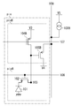
- Fig. 2 is an example of a schematic sectional view illustrating electrically-connecting portions of the first and second substrates that can be commonly adopted to the solid-state imaging device according to the present invention.
- a pixel region 203a is disposed on the second substrate 202.
- a pixel region 203b is disposed on a first substrate 201.
- a second peripheral region 204a is disposed on the second substrate 202.
- the second peripheral region 204a is disposed outside the pixel region 203a.
- a first peripheral region 204b is disposed on the first substrate 201.
- the first peripheral region 204b is disposed outside the pixel region 203b, and a circuit for processing a signal output from the pixel region 203b via a common output line or controlling a signal output from the pixel region is disposed.
- Fig. 2 illustrates a pixel amplifier 105, a FD 206, and a amplification transistor 207.
- the gate of the amplification transistor 207 and the FD 206 are electrically connected to each other.
- the amplification transistor 207 is illustrated as the pixel circuit, however, additionally, the above-described reset transistor is included in the pixel circuit.
- a MOS transistor 208 constitutes a part of the readout circuit disposed in the first peripheral region 204b.
- An example of the readout circuit includes a parallel processing circuit for processing in parallel the signals read from each column of a plurality of pixel columns.
- Such a parallel processing circuit includes a column amplifier and a column AD converter.
- a MOS transistor 209 constitutes a circuit other than the parallel processing circuit disposed in the first peripheral region 204b.
- a first conductivity pattern 110 constitutes a current voltage supply wiring for supplying a direct current voltage to the MOS transistors 209 constituting the parallel processing circuit.
- the first conductivity pattern 110 extends in a direction of a depth of a paper surface and supplies the direct current voltage to the MOS transistors of each parallel processing circuit in common.
- the first conductivity pattern 110 is disposed outside the pixel region 203b.
- a second conductivity pattern 211 is disposed outside the pixel region 203a on the second substrate 202.
- An electrically-connecting portion 112 electrically connects the first conductivity pattern 110 and the second conductivity pattern 211.
- the electrically-connecting portion 112 can be constituted by forming the conductivity pattern with a top wiring layer on the first substrate 201 and that on the second substrate 202 and by electrically connecting them to each other.
- the second conductivity pattern 211 is disposed in the second peripheral region 204a on the second substrate 202.
- the second peripheral region 204a includes less circuit elements compared to those disposed in the first peripheral region 204b on the first substrate 201, or no circuit elements at all.
- an area of the second conductivity pattern 211 is preferably made larger than that of the first conductivity pattern 110 to decrease a resistance value while maintaining free wiring layout on the second substrate 202.
- An electrically-connecting portion 113 electrically connects the FD 206 to the amplification transistor 207.
- the second electrically-connecting portion 113 can be constituted by forming the conductivity pattern with the top wiring layer on the first substrate 201 and that on the second substrate 202 and by electrically connecting them to each other.
- a well 214 of the first conductivity type is provided with at least a source region and a drain region of the amplification transistor 207 for one pixel.
- the conductivity type of the well is a "P" type.
- the conductivity type of the well is the "N" type. More specifically, the well is formed of a semiconductor region having the opposite conductivity type of the source region and the drain region.
- Each well 214 is electrically separated from the adjacent well in at least one direction.
- one well is provided with the source regions and the drain regions of a plurality of amplification transistors included in one pixel column.
- the adjacent wells provided with the source regions and the drain regions of the amplification transistors included in the pixel column are separated from each other.
- one well is provided with the source regions and the drain regions of a plurality of amplification transistors included in one pixel row. In this case, the adjacent wells provided with the source regions and the drain regions of the amplification transistors included in the pixel row are separated from each other.
- one well is provided with the source region and the drain region of the amplification transistor included in one pixel.
- the well provided with the source region and the drain region of the amplification transistor included in the pixel is separated from the adjacent wells in the vertical direction and the horizontal direction.
- the above-described third exemplary embodiment is a typical example.
- the wells When the wells are separated for each pixel column and each pixel row, the wells may be further separated within one pixel column and one pixel row.
- separating the wells refers to that the semiconductor region of an opposite conductivity type to the adjacent wells 214 is disposed therebetween.
- an insulation member may be disposed.
- a semiconductor region 215 has the second conductivity type that is opposite to that of the well 214.
- the semiconductor region 215 of the second conductivity type is disposed between the adjacent wells 214 and electrically separates the wells.
- the semiconductor substrate itself, an epitaxial layer, or a semiconductor region formed by injecting ion can be used.
- the wells 214 disposed in the pixel region by a predetermined unit are separated.
- a decrease of the light receiving area of the photoelectric conversion unit due to separation of the wells can be suppressed.
- a first effect is improvement of a gain of the amplification transistor.
- a second effect is suppression of cross talk via the well 214.
- a third effect is suppression of increasing an FD capacitance.
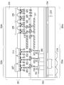
- Fig. 3 is a schematic top plan view illustrating a portion of the pixel circuit disposed on the second substrate.
- a selection transistor for selecting the amplification transistor, the reset transistor, or the pixel is disposed on the second substrate.
- a pixel region 301 is disposed on the second substrate.
- the above-described members included in the pixel are disposed with a predetermined repeating pitch.
- the pixel region 301 is separated into a grid-like shape so that the region occupied by one pixel can be schematically illustrated.
- Each pixel is disposed in a matrix.
- Wells 302 of the first conductivity type which are the "P" type herein, are separated for each pixel.
- the source regions and the drain regions of the amplification transistors, the reset transistors, and the selection transistors included in one pixel circuit are disposed in each well.
- the source region and the drain region are formed of the semiconductor region of the second conductivity type that is the opposite conductivity type of the well.
- a semiconductor region 303 of the second conductivity type which is the "N" type herein, is disposed at least between wells 302 to separate the well from the adjacent wells. Further, the semiconductor region 303 of the second conductivity type may be disposed at a bottom portion of each well 302.
- a control line 304 supplies a driving pulse to the gate of the reset transistor and the selection transistor included in the pixel circuit.
- the control line 304 is illustrated with one line in Fig. 3, however, actually two lines for the reset transistor and the selection transistor are disposed for each pixel column.
- a suffix indicates the row number.
- a vertical signal line 305 is used to read out the signals from pixel rows in parallel.
- the vertical signal line 305 is disposed for each pixel column.
- a suffix indicates the column number.
- Fig. 4 illustrates an example of an equivalent circuit of one pixel in a solid-state imaging device according to the present exemplary embodiment.
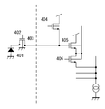
- Fig. 4 includes a photoelectric conversion unit 401, a transfer transistor 402 constituting a transfer unit, an FD 403, a reset transistor 404 constituting a pixel reset unit, a amplification transistor 405 constituting the pixel amplifier and a source follower circuit along with the current source, and a selection transistor 406 constituting a pixel selection unit.
- Figs. 1A, 1B and Fig. 4 includes the selection transistor.
- the photoelectric conversion unit 401, the transfer transistor 402, and the FD 403 are disposed on the first substrate, and the reset transistor 404, the amplification transistor 405, and a selection transistor 406 are disposed on the second substrate.
- the reset transistor 404, the amplification transistor 405, and the selection transistor 406 are constituted by the MOS transistor of the "N" type.
- Fig. 5 is a schematic top plan view of the second substrate. Same reference numerals are given to portions having the same functions as those in Figs. 3 and 4, and detailed descriptions will not be repeated.
- An electrically-connecting portion 501 is a portion for electrically connecting the second substrate to the first substrate.
- Polysilicon 502 forms a gate electrode of the amplification transistor and is electrically connected to the FD disposed on the first substrate via the electrically-connecting portion 501.
- a source region 503 is included in the amplification transistor.
- a drain region 504 is included in the amplification transistor and also functions as the source region of the selection transistor.
- Polysilicon 505 forms the gate electrode of the selection transistor.
- a source region 506 is included in the selection transistor.
- a source region 507 is included in the reset transistor.
- Polysilicon 508 forms the gate electrode of the reset transistor.
- a drain region 509 is included in the reset transistor.
- a semiconductor region 510 has the same conductivity type as those of the wells 302 and a higher impurity level than the wells 302. Since the semiconductor region 510 has a function for supplying a predetermined voltage to the wells, it is hereinafter referred to as a "well-contact region".
- a reset control line 511 supplies a driving pulse to the reset transistor.
- a reset power source line 512 is a line for supplying a reset voltage to the drain of the reset transistor.
- a selection control line 513 is a line for supplying the driving pulse to the gate of the selection transistor.
- a power source line 514 is a line for supplying a drain voltage to the drain of the amplification transistor.
- a vertical signal line 515 is also disposed on the second substrate.
- the amplification transistor performs the source follower operation.
- the charge generated by the photoelectric conversion unit 401 is supplied to the gate of the amplification transistor via the transfer transistor 402. Based on an amount of the supplied charge, the gate voltage of the amplification transistor is changed. Based on the change of the gate voltage of the amplification transistor, the source voltage of the amplification transistor is changed.
- the well 302 is electrically connected to the drain region 504 of the amplification transistor via the well-contact region 510. Accordingly, the potential of the well 302 changes for each pixel similar to the change of the voltage of the source of the amplification transistor.
- Fig. 6 illustrates a case where the well of the amplification transistor is grounded in an alternating-current manner as a comparison example and which is, for example, GND.
- Vgs the voltage between the gate and the source of the amplification transistor
- Vbs the voltage between the source and the back gate
- Rs the load resistance value
- Av represents the voltage gain of the source follower circuit
- gm and gmbs are respectively expressed as follows.
- gm Ids/Vgs
- gmbs Ids/Vbs
- Av gm/(gm + gmbs) (Equation 2)
- the value of the Equation 2 is normally within 08 to 0.9.
- the source of the amplification transistor is electrically connected to the wells.
- the voltage gain at this point is 1.0.
- the higher voltage gain can be acquired.
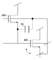
- Fig. 7 illustrates a part of a parasitic capacitance generated in the FD.
- Fig. 7 illustrates the reset transistor and the amplification transistor that are extracted from Fig. 4.
- a parasitic capacitance 701 is generated between the FD and the back gate of the reset transistor.
- the well and the source of the amplification transistor are electrically connected to each other, the voltage between the gate and the source of the amplification transistor becomes substantially constant despite of the FD potential. Therefore, the parasitic capacitance 701 does not contribute to the FD capacitance. This is because the well changes its voltage similar to that of the source of the amplification transistor.
- the FD capacitance can be reduced, thereby improving sensitivity of the solid-state imaging device.
- the selection transistor is disposed between the vertical output line and the source of the amplification transistor. With such a structure, the selection transistor becomes nonconductive so that influence on the well from the potential change of the vertical output line can be reduced, which is preferable.
- the wells of the transistor included in the pixel circuit disposed on the second substrate on which the photoelectric conversion unit is not disposed are separated for each pixel.
- the wells can be separated without decreasing the light receiving area of the photoelectric conversion unit.
- the voltage gain of the amplification transistor can be improved.
- the FD capacitance can be decreased.
- the selection transistor and by electrically separating the vertical output line from the source of the amplification transistor, the influence on the well from the potential change of the vertical output line can be decreased.
- a difference between the present exemplary embodiment and the first exemplary embodiment is that the wells are separated between the pixel columns.
- the wells are separated between the columns of the amplification transistors.
- a difference from the first exemplary embodiment is that the present exemplary embodiment includes no selection transistor.
- the structure illustrated in Fig. 1 can be adopted.
- Fig. 8 is a schematic top plan view illustrating a solid-state imaging device of a second exemplary embodiment.
- a pixel region 801 is disposed on the second substrate.
- the transistors included in the pixel illustrated with the equivalent circuit diagram are disposed with a predetermined repeating pitch.
- the pixel region is separated into a grid-like shape so that the region occupied by one pixel can be schematically illustrated.
- Each pixel is disposed in a matrix.
- Wells 802 of the first conductivity type which are the "P" type herein, are separated for each pixel.
- Each well is provided with the source regions and the drain regions of a plurality of amplification transistors and a plurality of the reset transistors that are included in one pixel column.
- the source region and the drain region are formed of the semiconductor regions of the second conductivity type.
- a semiconductor region 803 of the second conductivity type which is the "N" type herein, is disposed in a slit shape at least between wells 802 to separate the wells. Further, the semiconductor region 803 of the second conductivity type may be disposed at the bottom portion of each well 802.
- a control line 804 is a line for supplying the driving pulse to the gate of the reset transistor included in the pixel circuit.
- a suffix indicates the row number.
- a vertical signal line 805 is a line for reading the signals from each pixel row in parallel, and is disposed for each pixel column.
- a suffix indicates the column number.
- the area for one pixel on the second substrate can be decreased. Further, since no selection transistor is disposed on the second substrate, the area for the selection transistor can be also decreased.
- the wells may be separated at least between a plurality of pixels that simultaneously perform reading.
- the signals of a plurality of pixels included in the same pixel row are substantially simultaneously read by the corresponding vertical output line.
- a plurality of pixel signals included in a certain pixel row are substantially simultaneously read.
- the wells are separated for each pixel column and, then, the adjacent pixels in the same pixel row are disposed in the different wells.
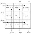
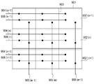
- FIG. 9 is a schematic top plan view illustrating the second substrate of a solid-state imaging device of the present exemplary embodiment.
- a pixel region 901 is disposed on the second substrate.
- the transistors included in the pixel indicated in the equivalent circuit diagram are disposed with a predetermined repeating pitch.
- the pixel region is separated into a grid-like shape so that the region occupied by one pixel can be schematically illustrated.
- Each pixel is disposed in a matrix.
- Wells 902 of the first conductivity type which are the "P" type herein, are separated for each pixel.
- a suffix indicates the row number.
- the source regions and the drain regions of a plurality of the amplification transistors and a plurality of the reset transistors included in one pixel row are disposed in each well.
- the source region and the drain region are formed of the semiconductor region of the second conductivity type.
- a semiconductor region 903 of the second conductivity type which is the "N" type herein, is disposed in a slit-like shape at least between wells 902 to separate the wells. Further, the semiconductor region 903 of the second conductivity type may be disposed at the bottom portion of each well 802.
- a control line 904 is a line for supplying a driving pulse to a gate of the reset transistor included in the pixel circuit.
- a suffix indicates the row number.
- a vertical signal line 905 is a line for reading the signals from the pixel rows in parallel and arranged for each pixel column.
- a suffix indicates the column number.
- a control line 906 is a line for supplying at least a first voltage and a second voltage to the wells separated for each pixel row.
- a predetermined voltage is supplied to the control line 906 from a voltage supply unit (not illustrated).
- the voltage supply unit includes, for example, a vertical scanning circuit, a timing generator, and a power source supply unit.
- the pixel by selectively supplying the first voltage or the second voltage for the control line 906 according to a reading pixel row or a non-reading pixel row, the pixel can be selected. More specifically, by changing a threshold value of the amplification transistor by the voltage supplied to the well, the pixel is selected.
- the MOS transistor of the "N" type When the MOS transistor of the "N" type is used for the amplification transistor, the first voltage is supplied to the well of the reading pixel row and the second voltage, which is higher than the first voltage, is supplied to the non-reading pixel row. With this arrangement, the signals of the reading pixel row is read out to the vertical output line selectively.
- each exemplary embodiment the transistor of the conductivity type of the "N" type included in the pixel circuit is described, however, the transistor of a "P" type can be also used.
- each semiconductor region may have the opposite conductivity type.
- the electrons and the holes generated by the photoelectric conversion unit the electrons are used as the signal charge has been described, and the holes can be also used. Further, by locally disposing a region having the high impurity density as the semiconductor region for separating the wells, the separation characteristic may be enhanced.
Landscapes
- Physics & Mathematics (AREA)
- Engineering & Computer Science (AREA)
- Power Engineering (AREA)
- Electromagnetism (AREA)
- Condensed Matter Physics & Semiconductors (AREA)
- General Physics & Mathematics (AREA)
- Computer Hardware Design (AREA)
- Microelectronics & Electronic Packaging (AREA)
- Solid State Image Pick-Up Elements (AREA)
- Transforming Light Signals Into Electric Signals (AREA)
Abstract
L'objectif de la présente invention est de proposer une structure de séparation préférable de puits lorsqu'une unité de conversion photoélectrique et une partie d'une unité de circuit périphérique ou d'un circuit de pixels sont formées de manière séparée sur des substrats séparés et connectées électriquement les unes aux autres. À cette fin, un dispositif d'imagerie à semi-conducteurs comprend une pluralité de pixels comprenant une unité de conversion photoélectrique et un transistor d'amplification configuré pour amplifier un signal généré par l'unité de conversion photoélectrique ; un premier substrat sur lequel une pluralité des unités de conversion photoélectrique sont disposées ; et un second substrat sur lequel une pluralité des transistors d'amplification sont disposés. Un puits d'un premier type de conductivité comportant une région de source et une région de drain du transistor d'amplification est séparé d'un puits, disposé adjacent au puits dans au moins une direction, du premier type de conductivité comportant la région de source et la région de drain du transistor d'amplification.
Priority Applications (1)
| Application Number | Priority Date | Filing Date | Title |
|---|---|---|---|
| US13/807,207 US8878267B2 (en) | 2010-07-02 | 2011-06-27 | Solid-state imaging device |
Applications Claiming Priority (2)
| Application Number | Priority Date | Filing Date | Title |
|---|---|---|---|
| JP2010-151973 | 2010-07-02 | ||
| JP2010151973A JP2012015400A (ja) | 2010-07-02 | 2010-07-02 | 固体撮像装置 |
Publications (1)
| Publication Number | Publication Date |
|---|---|
| WO2012001939A1 true WO2012001939A1 (fr) | 2012-01-05 |
Family
ID=45401681
Family Applications (1)
| Application Number | Title | Priority Date | Filing Date |
|---|---|---|---|
| PCT/JP2011/003643 WO2012001939A1 (fr) | 2010-07-02 | 2011-06-27 | Dispositif d'imagerie à semi-conducteurs |
Country Status (3)
| Country | Link |
|---|---|
| US (1) | US8878267B2 (fr) |
| JP (1) | JP2012015400A (fr) |
| WO (1) | WO2012001939A1 (fr) |
Cited By (7)
| Publication number | Priority date | Publication date | Assignee | Title |
|---|---|---|---|---|
| CN103367377A (zh) * | 2012-04-04 | 2013-10-23 | 索尼公司 | 固态成像装置和电子设备 |
| WO2013164717A1 (fr) * | 2012-04-30 | 2013-11-07 | Koninklijke Philips N.V. | Détecteur d'imagerie à isolation de puits de canal analogique par pixel avec découplage |
| WO2014013696A1 (fr) * | 2012-07-18 | 2014-01-23 | Sony Corporation | Dispositif d'imagerie à semi-conducteurs et appareil électronique |
| RU2686867C2 (ru) * | 2014-06-10 | 2019-05-06 | Конинклейке Филипс Н.В. | Модульная asic детектора визуализации |
| US10852183B2 (en) | 2015-11-19 | 2020-12-01 | Sony Semiconductors Solutions Corporation | Optical pulse detection device, optical pulse detection method, radiation counter device, and biological testing device |
| US11955502B2 (en) | 2018-09-11 | 2024-04-09 | Sony Semiconductor Solutions Corporation | Solid-state image sensor to reduce display unevenness of a captured image |
| US12052525B2 (en) | 2019-06-26 | 2024-07-30 | Sony Semiconductor Solutions Corporation | Three-dimensionally structured imaging device |
Families Citing this family (10)
| Publication number | Priority date | Publication date | Assignee | Title |
|---|---|---|---|---|
| JP6018376B2 (ja) * | 2011-12-05 | 2016-11-02 | キヤノン株式会社 | 固体撮像装置およびカメラ |
| US9406711B2 (en) * | 2012-06-15 | 2016-08-02 | Taiwan Semiconductor Manufacturing Company, Ltd. | Apparatus and method for backside illuminated image sensors |
| WO2014002367A1 (fr) * | 2012-06-25 | 2014-01-03 | パナソニック株式会社 | Dispositif de détection d'image à semi-conducteurs |
| JP6083977B2 (ja) * | 2012-08-23 | 2017-02-22 | オリンパス株式会社 | 固体撮像装置および撮像装置 |
| JP7178605B2 (ja) * | 2017-03-22 | 2022-11-28 | パナソニックIpマネジメント株式会社 | 固体撮像装置 |
| WO2019130702A1 (fr) * | 2017-12-27 | 2019-07-04 | ソニーセミコンダクタソリューションズ株式会社 | Dispositif de capture d'images |
| JP7452962B2 (ja) * | 2018-11-16 | 2024-03-19 | ソニーセミコンダクタソリューションズ株式会社 | 撮像装置 |
| JPWO2020179494A1 (fr) * | 2019-03-07 | 2020-09-10 | ||
| TW202109615A (zh) * | 2019-06-26 | 2021-03-01 | 日商索尼半導體解決方案公司 | 攝像裝置 |
| US11973102B2 (en) * | 2019-11-29 | 2024-04-30 | Sony Semiconductor Solutions Corporation | Imaging device and electronic apparatus |
Citations (4)
| Publication number | Priority date | Publication date | Assignee | Title |
|---|---|---|---|---|
| JP2002270807A (ja) * | 2001-03-08 | 2002-09-20 | Victor Co Of Japan Ltd | Cmosイメージセンサ |
| JP2003142672A (ja) * | 2001-10-31 | 2003-05-16 | Mitsubishi Electric Corp | 固体イメージセンサ及び固体イメージセンサの製造方法 |
| JP2008536330A (ja) * | 2005-04-13 | 2008-09-04 | シリコンファイル・テクノロジーズ・インコーポレイテッド | 3次元構造を有するイメージセンサの分離型単位画素及びその製造方法 |
| JP2010103547A (ja) * | 2009-12-11 | 2010-05-06 | Sony Corp | 固体撮像素子及びその制御方法 |
Family Cites Families (9)
| Publication number | Priority date | Publication date | Assignee | Title |
|---|---|---|---|---|
| US5192920A (en) * | 1992-03-18 | 1993-03-09 | Eastman Kodak Company | High-sensitivity, low-noise transistor amplifier |
| JP3596749B2 (ja) | 1999-12-01 | 2004-12-02 | 日本ビクター株式会社 | Cmosイメージセンサ |
| JP2004071683A (ja) * | 2002-08-02 | 2004-03-04 | Amtex Corp | 半田付装置 |
| JP3951879B2 (ja) * | 2002-10-04 | 2007-08-01 | ソニー株式会社 | 固体撮像素子及びその駆動方法 |
| JP2006196729A (ja) | 2005-01-14 | 2006-07-27 | Sony Corp | 固体撮像装置およびその製造方法 |
| US7482646B2 (en) * | 2006-10-18 | 2009-01-27 | Hejian Technology (Suzhou) Co., Ltd. | Image sensor |
| JP2008235478A (ja) | 2007-03-19 | 2008-10-02 | Nikon Corp | 撮像素子 |
| JP5985136B2 (ja) * | 2009-03-19 | 2016-09-06 | ソニー株式会社 | 半導体装置とその製造方法、及び電子機器 |
| KR101648200B1 (ko) * | 2009-10-22 | 2016-08-12 | 삼성전자주식회사 | 이미지 센서 및 그 제조 방법 |
-
2010
- 2010-07-02 JP JP2010151973A patent/JP2012015400A/ja active Pending
-
2011
- 2011-06-27 WO PCT/JP2011/003643 patent/WO2012001939A1/fr active Application Filing
- 2011-06-27 US US13/807,207 patent/US8878267B2/en active Active
Patent Citations (4)
| Publication number | Priority date | Publication date | Assignee | Title |
|---|---|---|---|---|
| JP2002270807A (ja) * | 2001-03-08 | 2002-09-20 | Victor Co Of Japan Ltd | Cmosイメージセンサ |
| JP2003142672A (ja) * | 2001-10-31 | 2003-05-16 | Mitsubishi Electric Corp | 固体イメージセンサ及び固体イメージセンサの製造方法 |
| JP2008536330A (ja) * | 2005-04-13 | 2008-09-04 | シリコンファイル・テクノロジーズ・インコーポレイテッド | 3次元構造を有するイメージセンサの分離型単位画素及びその製造方法 |
| JP2010103547A (ja) * | 2009-12-11 | 2010-05-06 | Sony Corp | 固体撮像素子及びその制御方法 |
Cited By (15)
| Publication number | Priority date | Publication date | Assignee | Title |
|---|---|---|---|---|
| CN103367377A (zh) * | 2012-04-04 | 2013-10-23 | 索尼公司 | 固态成像装置和电子设备 |
| US9318524B2 (en) | 2012-04-30 | 2016-04-19 | Koninklijke Philips N.V. | Imaging detector with per pixel analog channel well isolation with decoupling |
| WO2013164717A1 (fr) * | 2012-04-30 | 2013-11-07 | Koninklijke Philips N.V. | Détecteur d'imagerie à isolation de puits de canal analogique par pixel avec découplage |
| CN104272460A (zh) * | 2012-04-30 | 2015-01-07 | 皇家飞利浦有限公司 | 具有带去耦合的每像素模拟沟道阱隔离的成像探测器 |
| US9508770B2 (en) | 2012-07-18 | 2016-11-29 | Sony Corporation | Solid-state imaging device and electronic apparatus |
| CN104428897A (zh) * | 2012-07-18 | 2015-03-18 | 索尼公司 | 固态成像装置和电子设备 |
| WO2014013696A1 (fr) * | 2012-07-18 | 2014-01-23 | Sony Corporation | Dispositif d'imagerie à semi-conducteurs et appareil électronique |
| US20170062499A1 (en) * | 2012-07-18 | 2017-03-02 | Sony Corporation | Solid-state imaging device and electronic apparatus |
| CN108281451A (zh) * | 2012-07-18 | 2018-07-13 | 索尼公司 | 固态成像装置和电子设备 |
| US11482565B2 (en) | 2012-07-18 | 2022-10-25 | Sony Group Corporation | Solid-state imaging device and electronic apparatus |
| US12062682B2 (en) | 2012-07-18 | 2024-08-13 | Sony Group Corporation | Solid-state imaging device and electronic apparatus |
| RU2686867C2 (ru) * | 2014-06-10 | 2019-05-06 | Конинклейке Филипс Н.В. | Модульная asic детектора визуализации |
| US10852183B2 (en) | 2015-11-19 | 2020-12-01 | Sony Semiconductors Solutions Corporation | Optical pulse detection device, optical pulse detection method, radiation counter device, and biological testing device |
| US11955502B2 (en) | 2018-09-11 | 2024-04-09 | Sony Semiconductor Solutions Corporation | Solid-state image sensor to reduce display unevenness of a captured image |
| US12052525B2 (en) | 2019-06-26 | 2024-07-30 | Sony Semiconductor Solutions Corporation | Three-dimensionally structured imaging device |
Also Published As
| Publication number | Publication date |
|---|---|
| US8878267B2 (en) | 2014-11-04 |
| US20130105871A1 (en) | 2013-05-02 |
| JP2012015400A (ja) | 2012-01-19 |
Similar Documents
| Publication | Publication Date | Title |
|---|---|---|
| US8878267B2 (en) | Solid-state imaging device | |
| US9257472B2 (en) | Solid-state imaging device, camera, and design method for solid-state imaging device | |
| US8817151B2 (en) | Solid-state imaging device and method for solid-state imaging device for transferring charge from a photoelectric conversion portion to a floating diffusion | |
| JP5529613B2 (ja) | 光電変換装置及び撮像システム | |
| JP5780711B2 (ja) | 固体撮像装置 | |
| JP5538876B2 (ja) | 固体撮像装置 | |
| US20160134825A1 (en) | Solid-state image sensor and camera | |
| US9177979B2 (en) | Solid-state image pickup device having reference voltage supply line on a first substrate and power supply lines to supply voltages to the reference voltage supply line on a second substrate | |
| EP2978021A2 (fr) | Dispositif d'imagerie et son procédé de commande | |
| US9197832B2 (en) | Solid-state image pickup apparatus and drive method therefor | |
| US9196643B2 (en) | Solid-state imaging device having photoelectric conversion units on a first substrate and a plurality of circuits on a second substrate | |
| US9276021B2 (en) | Electronic device including current sources and amplifiers | |
| US9848145B2 (en) | Imaging device including pixels | |
| JP6497541B2 (ja) | 撮像装置 | |
| JP6526159B2 (ja) | 固体撮像装置およびカメラ | |
| US9711547B2 (en) | Image pickup apparatus | |
| JP6257726B2 (ja) | 固体撮像装置およびカメラ | |
| JP6355401B2 (ja) | 固体撮像装置及びカメラ | |
| US9659988B2 (en) | Image pickup apparatus | |
| JP6775206B2 (ja) | 撮像装置 | |
| JP2008071822A (ja) | Mos型固体撮像装置 | |
| JP4618170B2 (ja) | 固体撮像装置 | |
| JP2014154562A (ja) | 固体撮像装置、その製造方法、及び撮像システム | |
| WO2018176490A1 (fr) | Capteur d'image cmos ayant une commande d'exposition d'adresse xy | |
| JP4678270B2 (ja) | 固体撮像素子 |
Legal Events
| Date | Code | Title | Description |
|---|---|---|---|
| 121 | Ep: the epo has been informed by wipo that ep was designated in this application |
Ref document number: 11800409 Country of ref document: EP Kind code of ref document: A1 |
|
| WWE | Wipo information: entry into national phase |
Ref document number: 13807207 Country of ref document: US |
|
| NENP | Non-entry into the national phase |
Ref country code: DE |
|
| 122 | Ep: pct application non-entry in european phase |
Ref document number: 11800409 Country of ref document: EP Kind code of ref document: A1 |