WO2012001796A1 - 個体別情報生成装置及び個体別情報生成方法 - Google Patents
個体別情報生成装置及び個体別情報生成方法 Download PDFInfo
- Publication number
- WO2012001796A1 WO2012001796A1 PCT/JP2010/061211 JP2010061211W WO2012001796A1 WO 2012001796 A1 WO2012001796 A1 WO 2012001796A1 JP 2010061211 W JP2010061211 W JP 2010061211W WO 2012001796 A1 WO2012001796 A1 WO 2012001796A1
- Authority
- WO
- WIPO (PCT)
- Prior art keywords
- individual
- output
- specific information
- random number
- circuit
- Prior art date
Links
Images


Classifications
-
- G—PHYSICS
- G06—COMPUTING; CALCULATING OR COUNTING
- G06F—ELECTRIC DIGITAL DATA PROCESSING
- G06F7/00—Methods or arrangements for processing data by operating upon the order or content of the data handled
- G06F7/58—Random or pseudo-random number generators
- G06F7/582—Pseudo-random number generators
-
- G—PHYSICS
- G06—COMPUTING; CALCULATING OR COUNTING
- G06F—ELECTRIC DIGITAL DATA PROCESSING
- G06F7/00—Methods or arrangements for processing data by operating upon the order or content of the data handled
- G06F7/58—Random or pseudo-random number generators
- G06F7/588—Random number generators, i.e. based on natural stochastic processes
-
- G—PHYSICS
- G09—EDUCATION; CRYPTOGRAPHY; DISPLAY; ADVERTISING; SEALS
- G09C—CIPHERING OR DECIPHERING APPARATUS FOR CRYPTOGRAPHIC OR OTHER PURPOSES INVOLVING THE NEED FOR SECRECY
- G09C1/00—Apparatus or methods whereby a given sequence of signs, e.g. an intelligible text, is transformed into an unintelligible sequence of signs by transposing the signs or groups of signs or by replacing them by others according to a predetermined system
-
- H—ELECTRICITY
- H04—ELECTRIC COMMUNICATION TECHNIQUE
- H04L—TRANSMISSION OF DIGITAL INFORMATION, e.g. TELEGRAPHIC COMMUNICATION
- H04L9/00—Cryptographic mechanisms or cryptographic arrangements for secret or secure communications; Network security protocols
- H04L9/08—Key distribution or management, e.g. generation, sharing or updating, of cryptographic keys or passwords
- H04L9/0861—Generation of secret information including derivation or calculation of cryptographic keys or passwords
- H04L9/0866—Generation of secret information including derivation or calculation of cryptographic keys or passwords involving user or device identifiers, e.g. serial number, physical or biometrical information, DNA, hand-signature or measurable physical characteristics
-
- H—ELECTRICITY
- H04—ELECTRIC COMMUNICATION TECHNIQUE
- H04L—TRANSMISSION OF DIGITAL INFORMATION, e.g. TELEGRAPHIC COMMUNICATION
- H04L9/00—Cryptographic mechanisms or cryptographic arrangements for secret or secure communications; Network security protocols
- H04L9/32—Cryptographic mechanisms or cryptographic arrangements for secret or secure communications; Network security protocols including means for verifying the identity or authority of a user of the system or for message authentication, e.g. authorization, entity authentication, data integrity or data verification, non-repudiation, key authentication or verification of credentials
- H04L9/3271—Cryptographic mechanisms or cryptographic arrangements for secret or secure communications; Network security protocols including means for verifying the identity or authority of a user of the system or for message authentication, e.g. authorization, entity authentication, data integrity or data verification, non-repudiation, key authentication or verification of credentials using challenge-response
- H04L9/3278—Cryptographic mechanisms or cryptographic arrangements for secret or secure communications; Network security protocols including means for verifying the identity or authority of a user of the system or for message authentication, e.g. authorization, entity authentication, data integrity or data verification, non-repudiation, key authentication or verification of credentials using challenge-response using physically unclonable functions [PUF]
-
- H—ELECTRICITY
- H04—ELECTRIC COMMUNICATION TECHNIQUE
- H04L—TRANSMISSION OF DIGITAL INFORMATION, e.g. TELEGRAPHIC COMMUNICATION
- H04L9/00—Cryptographic mechanisms or cryptographic arrangements for secret or secure communications; Network security protocols
- H04L9/08—Key distribution or management, e.g. generation, sharing or updating, of cryptographic keys or passwords
- H04L9/0861—Generation of secret information including derivation or calculation of cryptographic keys or passwords
- H04L9/0869—Generation of secret information including derivation or calculation of cryptographic keys or passwords involving random numbers or seeds
Definitions
- the embodiment discussed in this specification relates to a technique for generating individual-specific information that is unique to each device and is different between devices.
- a clone product is a product having functions equivalent to those of a regular product manufactured using the results of analysis of the internal structure of a regular product, analysis of an IC chip existing inside the regular product, and the like.
- these clones there are many cases of infringing on the intellectual property rights of authorized manufacturers that manufacture genuine products, and anti-clone technology is strongly demanded.
- PUF Physical Unclonable Function
- PUF is a function that returns a different output for each device in which a PUF is mounted for a certain same input. However, it is not necessary to individually set functions that output different values for each device, and the same circuit realizes this function. In other words, the PUF circuit uses a slight difference in physical characteristics such as signal delay and element characteristics in the device to make its output completely different for each device. Therefore, this output is a value unique to the device (referred to as “individual information”).
- the device When an ideal PUF circuit is mounted on a device, the device always outputs the same individual information (reproducibility), while the PUF mounted on different devices outputs completely different individual information (difference). sex).
- the output information of the PUF in such a device can be compared to human biological information such as “fingerprint”. Fingerprints have the same properties as the output information of an ideal PUF, in which the same person is invariable even with age (reproducibility), but completely different (difference) between different persons.
- This PUF is also used to generate identification information (ID) and an encryption key.
- ID identification information
- Many electronic device products require unique IDs individually. Conventionally, in many cases, an operation of writing a different value for each device as an ID is performed at the manufacturing stage. If a PUF is used to generate this ID, the cost of this writing work can be reduced.
- PUF Packet Data Management Function
- a smart card in which an integrated circuit for recording information is assembled on a card.
- an encryption function is also essential for a SIM (Subscriber Identification Module) card used for a mobile phone, a terminal connected to a wireless Internet, and the like. If the random number used to generate the encryption key used for encryption on these devices is generated using the PUF, the risk that the encryption key will be analyzed by an attacker is greatly reduced and the security is improved. Will improve.
- SIM Subscriber Identification Module
- FIG. 1 illustrates a circuit configuration example of an arbiter PUF.
- the arbiter PUF 10 includes a total of 2n 2-input 1-output selectors 11-0a, 11-0b, 11-1a, 11-1b, 11-2a, 11-2b,..., 11- (n-1) a, And 11- (n ⁇ 1) b, and a D-type flip-flop circuit 12.
- selector 11 the selectors 11-0a, 11-0b, 11-1a, 11-1b, 11-2a, 11-2b,. ) A and 11- (n ⁇ 1) b are collectively referred to as “selector 11”.
- the selectors 11-1a and 11-1b have a first input terminal connected to the output terminal of the selector 11-0a and a second input terminal connected to the output terminal of the selector 11-0b.
- the selectors 11-2a and 11-2b have the first input terminal connected to the output terminal of the selector 11-1a and the second input terminal connected to the output terminal of the selector 11-1b.
- the remaining selectors 11 are similarly connected.
- Cha [n-1: 0] is input to the selector 11.
- This value Cha [n ⁇ 1: 0] is called “challenge”, and gives an instruction to the selector 11 to select which of the two input terminals of the selector 11 is to be output to the output terminal. Is for.
- the selectors 11-1a and 11-1b are both input with cha [1].
- the operation to output to the output terminal shall be performed.
- the operation of outputting the received signal to the output terminal shall be performed. The same operation is performed for the other selectors 11.
- the D-type flip-flop circuit 12 is referred to as “arbiter”.
- the output terminal of the selector 11- (n-1) a is connected to the data input terminal D
- the output terminal of the selector 11- (n-1) b is connected to the clock input terminal CLK. It is connected.
- the output of the D-type flip-flop circuit 12 becomes the output R of the arbiter PUF10. Note that the D-type flip-flop circuit 12 is reset at initialization and the output is set to zero.
- the arbiter PUF 10 has a symmetrical configuration in which a total of 2n selectors 11 are connected in series and connected to the D-type flip-flop circuit 12. Note that the wiring length in the connection between the selectors 11 and in the connection between the selectors 11- (n-1) a and 11- (n-1) b and the D-type flip-flop circuit 12 is as long as possible. It is preferable to keep them equal so as to maintain symmetry.
- the arbiter PUF 10 is a circuit that implements a PUF using circuit delay.
- the arbiter PUF 10 receives an edge signal that causes a state change in the D-type flip-flop circuit 12 when input to the clock terminal of the D-type flip-flop circuit 12 as an input signal.
- this edge signal is a rising edge signal whose logic level changes from 0 to 1.
- the rising edge signal input to the arbiter PUF 10 is input to the first input terminal and the second input terminal of the selectors 11-0a and 11-0b. Then, the rising edge signal passes through the selector 11 through a path according to the value of the challenge cha [n ⁇ 1: 0], and then the data input terminal D and the clock input terminal CLK of the D-type flip-flop circuit 12 that is an arbiter. To arrive.
- the output of the D-type flip-flop circuit 12 at this time is determined depending on which of the data input terminal D and the clock input terminal CLK the change point of the rising edge signal from 0 to 1 arrives first, and this output is the arbiter PUF10. Output R. That is, if this change point arrives first at the clock input terminal CLK, the output R of the arbiter PUF 10 becomes 0. If this change point arrives first at the data input terminal CLK, the output R of the arbiter PUF 10 becomes 1.
- the arbiter PUF 10 has a symmetrical configuration in which a total of 2n selectors 11 are connected in series. Further, as described above, the wiring lengths between the elements are substantially equal. Accordingly, on the circuit logic, the rising edge signals arrive at the data input terminal D and the clock input terminal CLK of the D-type flip-flop circuit 12 at the same time, and the rising edge signals that arrive at both should be in phase. is there. However, in reality, rising edge signals may not arrive at the same time due to gate delay or wiring delay caused by mounting conditions on the electronic device. The degree of the difference in arrival time is unique to the electronic device, but varies depending on the device. In other words, this degree of arrival time deviation has both the reproducibility and the difference, which are the properties of the PUF described above, and can be used as individual-specific information of an electronic device in which the arbiter PUF 10 is mounted.
- the arbiter PUF 10 shown in FIG. 1 inputs an edge signal that causes a state change in the D-type flip-flop circuit 12 to the clock terminal, and outputs an edge signal that is logically in phase with the edge signal. It is configured to input to the data input terminal.
- the signal output from the output terminal of the D-type flip-flop circuit 12 is configured to be the output of the arbiter PUF10.
- the arbiter PUF 10 can change the path through the selector 11 for the rising edge signal according to the value of the challenge Cha [n-1: 0]. Therefore, changing the value of the challenge Cha [n-1: 0] gives a different output R value. This output is referred to as “response”.
- the relationship between the challenge Cha [n-1: 0] and the response R in the arbiter PUF 10 mounted on a specific device is checked and recorded in advance. In this way, if the relationship between the challenge Cha [n-1: 0] of the arbiter PUF 10 of the device to be inspected and the response R is checked and compared with the above-mentioned recorded content, the device to be inspected can be identified. It is possible to authenticate whether or not the device is a device.
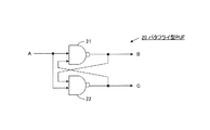
- the butterfly type PUF realizes a PUF using a metastable of an RS latch circuit.
- the metastable will be described with reference to FIGS. 2A and 2B.
- FIG. 2A illustrates a circuit configuration example of the RS latch circuit.
- This RS latch circuit is configured using NAND (Negative AND) circuits 21 and 22.
- the input of this RS latch circuit is negative logic.
- a negative logic signal is represented by adding an overbar on the signal name.
- a negative logic signal is represented by “#”. Therefore, for example, the set input of the RS latch circuit of FIG. 2A is expressed as “#S”, and the reset input is expressed as “#R”.
- the set input “#S” and the output of the NAND circuit 22 are input to the two inputs of the NAND circuit 21, respectively. Further, the reset input “#R” and the output of the NAND circuit 21 are input to the two inputs of the NAND circuit 22, respectively. Further, the output of the NAND circuit 21 becomes the output Q of the RS latch circuit. The output “#Q” is output from the output of the NAND circuit 22.
- FIG. 2B is a truth table of the RS latch circuit of FIG. 2A.
- the set input S and the reset input R are expressed in positive logic.
- the output logic of the RS latch circuit of FIG. 2A is stable if it is one of the above input combinations.
- both outputs of the RS latch circuit are in an unstable state of the intermediate potential.
- Such an unstable state that is abnormal as a digital circuit is called a metastable.
- FIG. 3 is a circuit configuration example of this butterfly type PUF.
- This butterfly type PUF 20 is configured to input the same value A to both the set input “#S” and the reset input “#R” of the RS latch circuit of FIG. 2A.
- the output Q and the output “#Q” of the RS latch circuit, which are outputs of the butterfly type PUF 20, are B and C, respectively. That is, the butterfly PUF 20 is a circuit configured to give an input for making a metastable state to the RS latch circuit, and to use a signal output from the output terminal of the RS latch circuit as an output of the butterfly PUF 20. It is.
- the output of this butterfly type PUF 20 takes one of two values (0 and 1).
- the butterfly-type PUF 20 when the butterfly-type PUF 20 is mounted on a device, there are three modes: one that always outputs 0, one that always outputs 1, and one whose output is not determined by 0 and 1, that is, one that outputs a random number.
- the output mode is reproducible. Therefore, a plurality of butterfly-type PUFs 20 can be mounted on the device, and the output obtained from each can be used as individual-specific information about the device on which the butterfly-type PUF 20 is mounted.
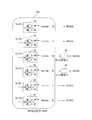
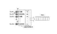
- FIG. 4 illustrates an individual-specific information generation apparatus that is a background art.
- the individual-specific information generation apparatus 30 is configured by mounting a plurality (n) of butterfly-type PUFs 20 illustrated in FIG. 3 on the device 1 which is an electronic device.
- FIG. 4 shows a state where a total of six butterfly PUFs 20 from “Latch 0” to “Latch 5” are selected by this challenge. Since the output RES [5: 0] of each of the six butterfly PUFs 20 has a binary value (0 or 1), these values are arranged to form a 6-bit bit string. This bit string becomes the response (characteristic value) described above, and can be used as individual information of the device 1. Note that the number of patterns of individual information that can be taken by the individual information generation apparatus 30 is 2 6 power patterns, that is, 64 patterns, because a total of six butterfly-type PUFs 20 are selected.
- the butterfly PUF 20 may output a random number.
- FIG. 4 represents a case where “latch 2” and “latch 3” out of a total of six butterfly PUFs 20 output random numbers. If such a butterfly type PUF 20 that outputs a random number is included in the selection by the challenge, the response that should be invariant in the device 1 may be different and the reproducibility is lost. It becomes unavailable.
- the individual-specific information generation apparatus 30 includes a code error correction circuit.
- a bit string formed by arranging the outputs of the butterfly type PUF 20 selected by the challenge is input to the code error correction circuit, and the output is used as a response of the individual-specific information generation apparatus 30. That is, the random number included in the bit string generated as described above from the butterfly-type PUF 20 is corrected by the code error correction circuit so that the device 1 always obtains the same response to the same challenge.
- the reproducibility of the output of the individual-specific information generation apparatus 30 is ensured in this way.
- the butterfly PUF 20 can be replaced with the arbiter PUF 10 in FIG. 1.
- the arbiter PUF10 also takes one of two values (0 and 1), but if the time difference between arrival of the rising edge signals at the data input terminal D and the clock input terminal CLK is extremely small, the output May be a random number. That is, the arbiter PUF 10 also outputs a predetermined fixed output value (0 or 1) or a random output value individually without the output for a specific input being uniquely determined, similarly to the butterfly type PUF 20. It is a digital circuit. Therefore, the correction by the code error correction circuit on the bit string generated from the output of the arbiter PUF 10 has an effect of ensuring reproducibility.
- the code error correction circuit In the individual-specific information generation apparatus 30 in FIG. 4, even if the code error correction circuit is provided as described above, the reproducibility of the individual-specific information may not be ensured. For example, consider a case where 128 individual PUFs 20 are mounted and the individual-specific information generation apparatus 30 is configured. In this case, if the number of butterfly-type PUFs 20 that output random numbers exceeds about 10, the code error correction circuit alone cannot absorb the difference in the value of the bit string formed by arranging the outputs of the butterfly-type PUF 20 side by side. There is. In other words, in this case, although the same device 1 is used, different responses are output for the same challenge, and since there is no reproducibility, it cannot be used as a PUF.
- the provision of the code error correction circuit as described above has a problem of increasing the mounting cost of the individual information generating apparatus 30.
- the present invention has been made in view of the above-described circumstances, and it is possible to generate individual-specific information having good reproducibility and difference with a small circuit scale.
- the individual-specific information generation device includes a plurality of digital circuits, a random number determination unit, and an individual-specific information generation unit.
- the plurality of digital circuits have the same circuit configuration.
- Each digital circuit outputs a predetermined constant output value or a random number output value individually without the output for a specific input being uniquely determined between the digital circuits.
- the order of each digital circuit is predefined.
- the random number determination unit determines, for each of the plurality of digital circuits, whether the output value is a random number or is constant. Then, the individual-specific information generation unit, based on the information and output values of the order defined in the digital circuit determined by the random number determination unit that the output value is constant among the plurality of digital circuits, Generate other information.
- one of the individual information generation methods described later in this specification is to generate individual information.
- this method first, it is determined for each of the plurality of digital circuits whether output values output from the plurality of digital circuits are random numbers or constant.
- the plurality of digital circuits have the same circuit configuration, and each digital circuit has an output for a specific input that is not uniquely determined between the digital circuits, but has a predetermined fixed output value or random number individually. Output the output value.
- Each digital circuit has a predefined order.
- the individual-specific information is generated based on the order information defined in the digital circuit in which the output value is determined to be constant among the plurality of digital circuits and the output value. .
- the individual-specific information generation apparatus described later in this specification can generate individual-specific information having good reproducibility and difference with a small circuit scale.
- arbiter PUF. 3 is a circuit configuration example of an RS latch circuit. It is a truth table of the RS latch circuit of FIG. 2A. It is a circuit structural example of a butterfly type PUF. It is an individual information generation apparatus of background art. It is a 1st example of the information generation apparatus classified by individual. It is a 1st example of the circuit structure of a random number determination part. It is a figure explaining operation
- FIG. 9 is a first example of a specific circuit configuration of a random number determination unit and an output conversion unit of the individual-specific information generation apparatus in FIG. 8. It is a 1st example of the circuit structure of a 1st conversion circuit. It is a 2nd example of the circuit structure of a 1st conversion circuit.
- FIG. 9 is a second example of a specific circuit configuration of a random number determination unit and an output conversion unit of the individual-specific information generation apparatus in FIG. 8. It is a 1st example of the circuit structure of a 2nd conversion circuit. It is a 2nd example of the circuit structure of a 2nd conversion circuit.
- FIG. 9 is a third example of a specific circuit configuration of the random number determination unit and the output conversion unit of the individual-specific information generation apparatus in FIG. 8.
- FIG. 11 is a diagram for explaining replacement of the circuit configuration of FIG. 10 from a butterfly PUF to an arbiter PUF.
- FIG. 13 is a diagram for explaining replacement of the circuit configuration of FIG. 12 from a butterfly PUF to an arbiter PUF.
- FIG. 15 is a diagram for explaining replacement of the circuit configuration of FIG. 14 from a butterfly PUF to an arbiter PUF. It is a 3rd example of the information generation apparatus classified by individual. It is a figure explaining operation
- FIG. 19 is a diagram illustrating replacement of the circuit configuration of FIG. 18 from a butterfly PUF to an arbiter PUF. It is a 4th example of the information generation apparatus classified by individual.
- FIG. 22 is a diagram for explaining replacement of the circuit configuration of FIG. 21 from a butterfly PUF to an arbiter PUF. It is a modification of the information generation apparatus classified by individual of FIG. It is a structural example of the encryption apparatus provided with the information generation apparatus classified by individual. It is a structural example of the authentication object apparatus provided with the information generation apparatus classified by individual. It is a structural example of an authentication apparatus.
- FIG. 5 illustrates a first example of the individual-specific information generation apparatus.
- This individual-specific information generation apparatus 100 is configured by mounting a plurality (n) of butterfly-type PUFs 20 and random number determination units 40 on a device 1 that is an electronic device, and further mounting an individual-specific information generation unit 50. Yes.
- the butterfly type PUF 20 has the same configuration as that shown in FIG. 3 and gives an input for setting the metastable state to the RS latch circuit, and outputs a signal output from the output terminal of the RS latch circuit to the output of the butterfly type PUF 20.
- This circuit is configured as follows. Note that the order is defined in advance for each of the n butterfly-type PUFs 20 having the same circuit configuration.
- This individual-specific information generation apparatus 100 also corresponds to the challenge described above to select which of the n butterfly-type PUFs 20 mounted.
- FIG. 5 represents a state where a total of six butterfly-type PUFs 20 are selected by this challenge.
- the random number determination unit 40 determines whether the output value of each butterfly PUF 20 is a random number or is constant.
- the individual-specific information generation unit 50 generates individual-specific information of the device 1 based on the information of the order defined in each of the butterfly-type PUFs 20 whose output value is determined to be constant by the random number determination unit 40. To do.
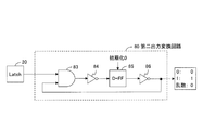
- FIG. 6 illustrates a first example of the circuit configuration of the random number determination unit 40.
- the random number determination unit 40 includes an AND circuit 41, NOT circuits 42 and 44, D-type flip-flop circuits 43 and 46, an OR circuit 45, and an ExOR circuit 47.
- the AND circuit 41 is a 2-input AND circuit.
- the output of the butterfly PUF 20 is input to one input of the AND circuit 41, and the output of the NOT (negative) circuit 44 is connected to the other input.
- the output of the AND circuit 41 is connected to the input of the NOT circuit 42, and the output of the NOT circuit 42 is connected to the data input of the D-type flip-flop circuit 43.
- the output of the D-type flip-flop circuit (hereinafter abbreviated as “D-FF”) 43 is connected to the input of the NOT circuit 44.
- OR circuit 45 is a 2-input OR circuit.
- the output of the butterfly PUF 20 is input to one input of the OR circuit 45, and the output of the D-FF 46 is connected to the other input.
- the output of the OR circuit 45 is connected to the data input of the D-FF 46.
- the ExOR circuit 47 is a 2-input exclusive OR circuit.
- the output of the NOT circuit 44 is connected to one input of the ExOR circuit 47, and the output of the D-FF 46 is connected to the other input.
- the output of the ExOR circuit 47 becomes the output of the random number determination unit 40.
- the D-FF 43 since the D-FF 43 has been initialized, its output is 0. Accordingly, at this time, since the two inputs of the AND circuit 41 are both 1, the output is 1. Then, 0 is input to the D-FF 43 by the action of the NOT circuit 42. Then, since the output of the D-FF 43 is also 0, the output of the NOT circuit 44 is 1.
- the operation of the random number determination unit 40 when the output of the butterfly PUF 20 is a random number (when the output is not determined to be either 0 or 1) will be described.
- the output of the D-FF 43 initialized to 0 becomes 1 when the output of the butterfly PUF 20 becomes 0, and therefore the output of the NOT circuit 44 becomes 0.
- the output of the D-FF 43 remains 1 and therefore the output of the NOT circuit 44 remains 0. Is done.
- the random number determination unit 40 determines whether the output of the butterfly PUF 20 is a random output value or a constant output value.
- the individual-specific information generation unit 50 in FIG. 5 arranges the outputs of the butterfly-type PUF 20 that have been determined by the random number determination unit 40 as being constant, according to the information on the order, thereby identifying the individual device 1 Generate information. At this time, the individual-specific information generation unit 50 discards the output (that is, the output value of the random number) of the butterfly-type PUF 20 for which the output value is determined to be a random number, Not used to generate information.
- FIG. 7 A total of six butterfly-type PUFs 20 from “Latch 0” to “Latch 5” illustrated in FIG. 7 are selected by the challenge, and the above-described order defined for those selected is “ The numbers from “Latch 0” to “Latch 5” are shown.
- FIG. 6 represents the case where “latch 2” and “latch 3” out of a total of six butterfly-type PUFs 20 output random number output values.
- the random number determination unit 40 determines that “latch 2” and “latch 3” out of a total of six butterfly-type PUFs 20 output output values of random numbers, and other output constant output values. And the determination result is transmitted to the individual-specific information generation unit 50. Then, the individual-specific information generation unit 50 discards the outputs of “Latch 2” and “Latch 3”, and outputs the outputs of “Latch 0”, “Latch 1”, “Latch 4”, and “Latch 5”. A bit string is generated by arranging in accordance with the order, and is output as individual information of the device 1.
- the individual-specific information generation apparatus 100 can generate and output individual-specific information of the device 1 by the individual-information generating unit 50 performing the above-described operation.
- the butterfly PUF 20 can be replaced with the arbiter PUF 10 in FIG. 1.
- the arbiter PUF 10 inputs an edge signal that causes a state change in the D-type flip-flop circuit 12 to its clock terminal, and outputs an edge signal that is logically in phase with the edge signal as its data input terminal. Is configured to input.
- the signal output from the output terminal of the D-type flip-flop circuit 12 is configured to be the output of the arbiter PUF10.
- the butterfly-type PUF 20 is connected to another digital circuit that performs the same operation, that is, an output for a specific input is not uniquely determined, but an individual predetermined output value or random output value. It is also possible to replace it with another digital circuit that outputs the signal.
- FIG. 8 illustrates a second example of the individual-specific information generation apparatus.
- the individual-specific information generation apparatus 200 in FIG. 8 is mounted on the device 1 that is an electronic device.
- the individual-specific information generation apparatus 200 inputs the outputs of the butterfly-type PUF 20 and the random number determination unit 40 to the output conversion unit 60 with respect to the individual-specific information generation apparatus 100 illustrated in FIG. This is a change to input to 50.
- the number of possible individual information patterns is 2 to the fourth power. There are fewer patterns, ie, 16 patterns. If the number of individual information patterns that can be taken is small, the possibility that the individual information is the same between different devices increases. This means that the above-described difference is low, and the range of use as a PUF is limited.
- the individual-specific information generation unit 50 adds each of the butterfly-type PUFs 20 determined by the random number determination unit 40 that the output value is a random number in addition to the operation of the first example described above. Based on the information of the defined order, the individual information of the device 1 is generated.
- the output conversion unit 60 converts the output of the butterfly-type PUF 20 that has been determined by the random number determination unit 40 to be a random number, to a predetermined value.
- the individual-specific information generation unit 50 outputs the output of the butterfly-type PUF 20 whose output value is determined to be constant by the random number determination unit 40 and the output converted by the output conversion unit 60.
- the individual-specific information is generated by arranging the predetermined values. When arranging the outputs, the outputs are arranged according to the order information defined in each of the butterfly-type PUFs 20.
- FIG. 9 represents the case where “latch 2” and “latch 3” out of a total of six butterfly-type PUFs 20 output random number output values.
- the random number determination unit 40 determines that “latch 2” and “latch 3” out of a total of six butterfly-type PUFs 20 output output values of random numbers, and other output constant output values. The determination result is transmitted to the output conversion unit 60. Then, the output conversion unit 60 converts the output values of the random numbers output from the “latch 2” and “latch 3” into a constant predetermined value, and the predetermined values after the conversion are “latch 2” and “latch 3”. Is output to the individual-specific information generation unit 50. The individual-specific information generation unit 50 arranges the outputs of “latch 0” to “latch 5” according to this order, generates a bit string, and outputs it as individual-specific information of the device 1.
- the individual-specific information generation apparatus 200 has a feature that the order information of the output value of the random number among the “latch” selected by the challenge is used for generating the individual-specific information. Yes.
- the number of individual information patterns that can be taken does not depend on whether or not the “latch” outputs a random number output value, and almost matches the number of “latch” to be mounted. You can have a number of patterns. More specifically, if the number of “latches” is N, the individual-specific information can take 2 N number of patterns. Therefore, the above-described decrease in difference is suppressed.
- FIG. 10 illustrates a first example of a specific circuit configuration of the random number determination unit 40 and the output conversion unit 60 of the individual-specific information generation apparatus 200 of FIG.
- FIG. 10 shows that the output of the butterfly type PUF 20 is input to the first conversion circuit 70, and the output of the first conversion circuit 70 is input to the individual-specific information generation unit 50.
- the first conversion circuit 70 combines the operations performed by each of the random number determination unit 40 and the output conversion unit 60 in FIG. That is, the first conversion circuit 70 determines whether the output value of the butterfly-type PUF 20 is a random number or is constant, and determines the output value of the butterfly-type PUF 20 that is determined to be a random number as a constant predetermined value “1”. ”To work.
- FIG. 11A and FIG. 11B are a first example and a second example of the circuit configuration of the first conversion circuit 70, respectively. First, the first example of FIG. 11A will be described.
- the first conversion circuit 70 includes an OR circuit 71 and a D-FF 72.
- the output of the butterfly PUF 20 is input to one input of an OR circuit 71 that is a two-input OR circuit, and the output of the D-FF 72 is connected to the other input.
- the output of the OR circuit 71 is connected to the input of the D-FF 72, and the output of the D-FF 72 becomes the output of the first conversion circuit 70.
- the D-FF 72 is reset at initialization and the output is set to zero.
- the D-FF 72 is initialized to 0. Therefore, the two inputs of the OR circuit 71 are both 0, so the output is 0. Since this output is input to the D-FF 72, the output of the D-FF 72 still remains zero. Accordingly, the output of the first conversion circuit 70 in this case is zero.
- the output of the butterfly type PUF 20 becomes 1 even for a short period, the output of the OR circuit 71 becomes 1, and this output is input to the D-FF 72, so the output of the D-FF 72 also becomes 1.
- the output of the OR circuit 71 remains 1 because the output of the D-FF 72 is 1. Therefore, the output of the D-FF 72 is kept at 1. The Therefore, in both cases where the output of the butterfly-type PUF 20 is always 1 and when the output value of the butterfly-type PUF 20 is a random number (when the output is not determined to be either 0 or 1), the first conversion circuit 70 The output of is 1.
- the first conversion circuit 70 in FIG. 11A uses the output of the butterfly type PUF 20 as its own output when the output of the butterfly type PUF 20 is always 0 and always 1, and the output value of the butterfly type PUF 20 is a random number. In this case, the output is converted into a predetermined value “1” and output.
- the first conversion circuit 70 includes NOT circuits 73 and 76, an AND circuit 74, and a D-FF 75.
- the output of the butterfly type PUF 20 is input to the input of the NOT circuit 73.
- the output of the NOT circuit 73 is connected to one input of an AND circuit 74 that is a 2-input AND circuit, and the output of the D-FF 75 is connected to the other input of the AND circuit 74.
- the output of the AND circuit 74 is connected to the input of the D-FF 75, and the output of the D-FF 75 is also connected to the input of the NOT circuit 76.
- the output of the NOT circuit 76 becomes the output of the first conversion circuit 70.
- the D-FF 75 is reset at the time of initialization and the output is set to 1.
- the output of the butterfly type PUF 20 is always 1 or the case where the output value of the butterfly type PUF 20 is a random number (when the output is not determined to be either 0 or 1).
- the output of the first conversion circuit 70 is 1.
- the first conversion circuit 70 in FIG. 11B also uses the output as it is, and the output value of the butterfly type PUF 20 is a random number. In this case, the output is converted into a predetermined value “1” and output.
- FIG. 12 illustrates a second example of a specific circuit configuration of the random number determination unit 40 and the output conversion unit 60 of the individual-specific information generation apparatus 200 of FIG.
- FIG. 12 shows that the output of the butterfly type PUF 20 is input to the second conversion circuit 80, and the output of the second conversion circuit 80 is input to the individual-specific information generation unit 50.
- the second conversion circuit 80 combines the operations performed by the random number determination unit 40 and the output conversion unit 60 in FIG. 8, similarly to the first conversion circuit 70 in FIG. 10. However, the second conversion circuit 80 determines whether the output value of the butterfly-type PUF 20 is a random number or is constant, and determines that the output value is a random number, but outputs the output to a constant predetermined value “0”. Works to convert to.
- FIG. 13A and FIG. 13B are a first example and a second example of the circuit configuration of the second conversion circuit 80, respectively. First, the first example of FIG. 13A will be described.
- the second conversion circuit 80 includes an AND circuit 81 and a D-FF 82.
- the output of the butterfly PUF 20 is input to one input of an AND circuit 81 which is a 2-input AND circuit, and the output of the D-FF 82 is connected to the other input.
- the output of the AND circuit 81 is connected to the input of the D-FF 82, and the output of the D-FF 82 becomes the output of the second conversion circuit 80.
- the D-FF 82 is reset at the time of initialization and the output is set to 1.
- the D-FF 82 When the output of the butterfly type PUF 20 is always 1, the D-FF 82 is initialized to 1. Accordingly, since both of the two inputs of the AND circuit 81 are 1, the output is 1. Since this output is input to the D-FF 82, the output of the D-FF 82 still remains at 1. Accordingly, the output of the second conversion circuit 80 in this case is 1.
- the second conversion circuit 80 in FIG. 13A uses the output of the butterfly type PUF 20 as its own output when the output of the butterfly type PUF 20 is always 0 and always 1, and the output value of the butterfly type PUF 20 is a random number. In this case, the output value is converted into a predetermined value “0” and output.
- the second conversion circuit 80 includes an AND circuit 83, NOT circuits 84 and 86, and a D-FF 85.
- the output of the butterfly PUF 20 is input to one input of the AND circuit 83 which is a 2-input AND circuit, and the output of the NOT circuit 86 is connected to the other input.
- the output of the AND circuit 83 is connected to the input of the NOT circuit 84, and the output of the NOT circuit 84 is connected to the input of the D-FF 85.
- the output of the D-FF 85 is connected to the input of the NOT circuit 86, and the output of the NOT circuit 86 becomes the output of the second conversion circuit 80.
- the D-FF 85 is reset at initialization and the output is set to zero.
- the second conversion circuit 80 in FIG. 13B also uses the output of the butterfly type PUF 20 as its own output when the output of the butterfly type PUF 20 is always 0 and always 1, and the output value of the butterfly type PUF 20 is a random number. In this case, the output is converted into a predetermined value “0” and output.
- FIG. 14 illustrates a third example of a specific circuit configuration of the random number determination unit 40 and the output conversion unit 60 of the individual-specific information generation apparatus 200 of FIG.
- the output conversion unit 60 sets the output of the butterfly type PUF 20 determined by the random number determination unit 40 as an output value to be a random number to a number representing an order predefined in the butterfly type PUF 20. It is configured to convert to a corresponding value.
- the circuit configuration of FIG. 14 is configured such that the output of the butterfly PUF 20 is input to one of the first conversion circuit 70 and the second conversion circuit 80 and the output is input to the individual-specific information generation unit 50. ing.
- the first conversion circuit 70 is the same as that of FIG. 10, and determines whether the output value of the butterfly PUF 20 is a random number or is constant, and the output value is determined to be a random number. It operates to convert the output to a constant predetermined value “1”. Therefore, the circuit configuration shown in FIGS. 11A and 11B can be used as the first conversion circuit 70 in FIG.
- the second conversion circuit 80 is also the same as that in FIG. 12, and determines whether the output value of the butterfly PUF 20 is a random number or constant, and the output value is determined to be a random number. It operates to convert the output to a constant predetermined value “0”. Therefore, the circuit configuration shown in FIGS. 13A and 13B can be used as the second conversion circuit 80 in FIG.
- FIG. 14 which of the first conversion circuit 70 and the second conversion circuit 80 is connected to the butterfly type PUF 20 is determined by a number representing an order previously defined for the butterfly type PUF 20. . More specifically, the first conversion circuit 70 is connected to the butterfly-type PUF 20 whose number representing the predefined order is an odd number, and the butterfly whose number representing the predefined order is an even number.
- a second conversion circuit 80 is connected to the type PUF 20. That is, in the configuration of FIG. 14, the output conversion unit 60 determines that the butterfly type number is an odd number when the number of the order defined in advance in the butterfly PUF 20 determined by the random number determination unit 40 as an output value is a random number. Set the output of the type PUF 20 to 1. Further, the output conversion unit 60 sets the output of the butterfly type PUF 20 to 0 when the number of the order previously defined in the butterfly type PUF 20 determined by the random number determination unit 40 as an output value is a random number. Set to.
- the butterfly-type PUF 20 can be replaced with the arbiter PUF 10 shown in FIG. 15, FIG. 16, and FIG. 17 are obtained by replacing the butterfly-type PUF 20 in the circuit configurations illustrated in FIGS. 10, 12, and 14 with an arbiter PUF 10, respectively.
- the butterfly type PUF 20 with the arbiter PUF 10 no other circuit configuration change is necessary and can be easily performed.
- FIG. 18 illustrates a third example of the individual-specific information generation apparatus.
- the individual-specific information generation apparatus 300 in FIG. 18 is mounted on the device 1 that is an electronic device.
- the individual-specific information generation apparatus 300 inputs each output of the butterfly PUF 20 to the random number determination unit 40 one by one, inputs each output to the entropy compression unit 90, and outputs the output of the entropy compression unit 90 to the individual It has the 1st structure inputted into another information generating part 50.
- the individual information generation apparatus 300 includes a configuration in which the individual information generation apparatus 100 of FIG. 5 is combined.
- the individual-specific information generation unit 50 selects each output of the butterfly-type PUF 20 using each output of the random number determination unit 40.
- the second configuration for generating the individual information of the device 1 is provided.
- the random number determination unit 40 in FIG. 18 the one illustrated in FIG. 6 is used. Therefore, when the butterfly type PUF 20 always outputs only one of 0 and 1, the random number determination unit 40 has an output value of 0, and when the butterfly type PUF 20 outputs a random number output value. The output value is 1. In this way, the random number determination unit 40 assigns one value 0 of the binary information to the butterfly PUF 20 determined to have a constant output value, and the output value of the butterfly PUF 20 is a random number. The other value 1 of the binary information is assigned to what is determined to be.
- the operation of the entropy compression unit 90 in FIG. 18 will be described with reference to FIG.
- the entropy compression unit 90 first generates a bit string by arranging values assigned by the random number determination unit 40 for each of the butterfly-type PUFs 20 according to information in an order defined in advance for each of the butterfly-type PUFs 20 as preprocessing. To do. Subsequently, the entropy compression unit 90 performs entropy compression on the bit string obtained by arranging in this way, and outputs the obtained value.
- a circuit that obtains a hash function value for the obtained bit string is used as the entropy compression unit 90. More specifically, as this circuit, a circuit for obtaining a hash function value by SHA-256, which is a hash function adopted in the Federal Information Processing Standards / FIPS, is used. Therefore, the output of the entropy compression unit 90 is a 256-bit bit string.
- a function such as LFSR (linear feedback shift register) or FUZZY EXTRACTOR may be used instead of the hash function.
- the bit string arranged by the entropy compression unit 90 as described above has N C T patterns. can get. Therefore, among the 256-bit output values output from the entropy compression unit 90, the entropy of bits corresponding to N CT bits can be used as individual-specific information. Accordingly, the individual-specific information generation unit 50 extracts a bit string corresponding to N C T bits from the output of the entropy compression unit 90 and outputs the obtained bit string as individual-specific information of the device 1.
- the individual-specific information generation unit 50 may output the 256-bit hash value output from the above-described entropy compression unit 90 as individual-specific information of the device 1 as it is.
- the individual-specific information generation apparatus 300 includes the configuration of the individual-specific information generation apparatus 100 in FIG. 5 as a second configuration for generating individual-specific information. Therefore, the individual information generation unit 50 in FIG. 18 is configured to have the same function as the individual information generation unit 50 in FIG. That is, the individual-type information of the device 1 is generated by arranging the outputs of the butterfly-type PUF 20 that are determined by the random number determination unit 40 to be constant according to the information of the order. At this time, for the butterfly-type PUF 20 whose output value is determined to be a random number by the random number determination unit 40, the output (that is, the output value of the random number) is discarded and is not used for generating individual-specific information. To. The individual-specific information generation unit 50 arranged the first individual-specific information generated as described above and the second individual-specific information generated as described above from the output of the entropy compression unit 90. The information may be output as individual information of the device 1.
- the above-described first individual-specific information has 2 NT patterns.
- the second individual-specific information described above as described above, a pattern of streets N C T obtained. Therefore, when the individual-specific information generation unit 50 generates the individual-specific information of the device 1 by arranging the first individual-specific information and the second individual-specific information as described above, 2 NT ⁇ N C T It becomes possible to obtain a pattern of street-specific information.
- the butterfly PUF 20 can be replaced with the arbiter PUF 10 in FIG. 1.
- FIG. 20 is obtained by replacing the butterfly type PUF 20 in the circuit configuration illustrated in each drawing of FIG. 18 with an arbiter PUF 10. As described above, when replacing the butterfly type PUF 20 with the arbiter PUF 10, no other circuit configuration change is necessary and can be easily performed.
- FIG. 21 illustrates a fourth example of the individual-specific information generation apparatus.
- the individual-specific information generation apparatus 400 in FIG. 21 is mounted on the device 1 that is an electronic device.
- the individual-specific information generation apparatus 400 has a configuration in which each output of the butterfly-type PUF 20 is input to the random number determination unit 40 one by one and each output is input to the individual-specific information generation unit 50.
- FIG. 22 illustrates a second example of the circuit configuration of the random number determination unit 40. This second example is used for the individual-specific information generation apparatus 400 of FIG.
- the random number determination unit 40 in FIG. 22 arranges the bits output from the NOT circuit 44 and the bits output from the D-FF 46 to form a bit string and outputs it. Therefore, the random number determination unit 40 outputs the bit string “00” when the output of the butterfly PUF 20 that is a binary output is always 0, and the bit string “11” when the output of the butterfly PUF 20 is always 1. Is output.
- the random number determination unit 40 outputs a bit string “10” when the output value of the butterfly PUF 20 is a random number. That is, the random number determination unit 40 also has a function as the output conversion unit 60. That is, the random number determination unit 40 converts the output of the butterfly-type PUF 20 that is determined to have an output value of a random number into the first bit string “10”.
- the random number determination unit 40 also converts the output of the butterfly-type PUF 20 whose output value is determined to be constant. In this conversion, when the output is 0, it is converted to a second bit string “00” different from the first bit string, and when the output is 1, the first bit string and the second bit string are different from each other. It is converted into a three-bit string “11”.
- the individual-specific information generation unit 50 arranges the outputs of the butterfly-type PUFs 20 converted into the bit strings as described above according to the information in the order defined in each of the butterfly-type PUFs 20, and stores the individual-specific information of the device 1. Generate. Accordingly, when the number of butterfly-type PUFs 20 used for generating the individual-specific information is N, 2N-bit individual-specific information is generated.
- the individual-specific information generation apparatus 400 in FIG. 21 responds to each case where the output of the butterfly-type PUF 20 is always 0, always 1, and when the output value is a random number. Individual different information of the device 1 is generated by assigning three different values. Therefore, many patterns can be obtained as individual-specific information.
- the butterfly-type PUF 20 can be replaced with the arbiter PUF 10 in FIG. FIG. 24 is obtained by replacing the butterfly PUF 20 in the circuit configuration illustrated in each drawing of FIG. 21 with an arbiter PUF 10. As described above, when replacing the butterfly type PUF 20 with the arbiter PUF 10, no other circuit configuration change is necessary and can be easily performed.
- the individual of FIG. 18 is interposed between the random number determination unit 40 (output conversion unit 60) and the individual-specific information generation unit 50.
- An entropy compression unit 90 similar to that in the other information generation apparatus 300 may be added.
- the entropy compression unit 90 performs entropy compression on a value obtained by arranging the outputs of the butterfly-type PUF 20 (or arbiter PUF 10) converted into a bit string by the output conversion unit 60 according to the above-described order information.
- the individual-specific information generation unit 50 generates the individual-specific information of the device 1 based on the value obtained by entropy compression by the entropy compression unit 90 when configured in this way.
- the number of patterns of the individual-specific information generated by the individual-specific information generating apparatus 100 becomes 2 120 ways.
- the individual information generation devices 30, 100, 200, 300, and 400 described above are configured by a combination of an arithmetic processing device and software executed by the arithmetic processing device, instead of the hardware. It is also possible to do.
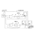
- FIG. 26 illustrates a configuration example of the encryption device.
- the encryption apparatus 500 is configured using any one of the individual information generation apparatuses 100, 200, 300, and 400. In the following description, a case where the encryption apparatus 500 uses the individual-specific information generation apparatus 100 of FIG. 5 will be described as an example.
- the encryption device 500 includes an individual information generation device 100, a CPU 510, a cryptographic operation unit 520, a ROM 530, and a RAM 540. Each of these components is connected to the bus line 550, and is configured to be able to exchange various data with each other under the management of the CPU 510.
- the individual-specific information generation apparatus 100 is mounted on the device 1 that is an electronic device.
- a CPU (Central Processing Unit) 510 is a central processing unit that manages the operation of each component of the encryption device 500.
- the cryptographic operation unit 520 performs encryption processing of various information and decryption processing of encrypted data.
- the cryptographic operation unit 520 includes a public key coprocessor 521 and a common key coprocessor 522.
- the public key coprocessor 521 performs encryption and decryption processing using RSA encryption, elliptic curve encryption, and the like, which are typical public key cryptosystems.
- the common key coprocessor 522 performs encryption and decryption processing using an AES cipher that is a typical common key cryptosystem.
- the encryption and decryption processing performed by the cryptographic operation unit 520 may be performed by the CPU 510.
- a ROM (Read Only Memory) 530 is a non-volatile semiconductor memory in which a control program executed by the CPU 510 and unique parameters used by the cryptographic computing unit 520 in encryption and decryption processing are stored in advance.
- the CPU 510 reads out this control program from the ROM 530 and starts its execution, whereby the operation management of each component of the encryption apparatus 500 can be performed. .
- a RAM (Random Access Memory) 540 is a volatile semiconductor memory that is used as a working storage area as necessary when the CPU 510 or the cryptographic operation unit 520 performs various processes.
- the cryptographic operation unit 520 performs information encryption processing using the individual information generated by the individual information generation device 100 as an encryption key.
- the individual-specific information used as the encryption key in this encryption process is also used for the decryption process that is subsequently performed on the encrypted information by the cryptographic operator 520.
- post-processing for further improving the entropy of the generated individual information may be performed.
- An example of post-processing performed for this purpose is the use of a linear feedback shift register (LFSR).
- the LFSR is a counter constituted by a shift register that is fed back by an exclusive OR circuit, and can improve the entropy of individual-specific information. Therefore, by generating the encryption key using the data string output from the LFSR, it becomes possible to generate an encryption key with higher randomness.
- the LFSR may be configured and used as dedicated hardware, or may be realized by software using the CPU 510.
- This authentication system is a system in which an authentication device performs authentication as to whether or not an authentication target device is authorized.
- FIG. 27 illustrates a configuration example of an authentication target device used in this authentication system.
- the authentication target device 600 is configured using any of the individual-specific information generation devices 100, 200, 300, and 400.
- the case where the authentication target device 600 uses the individual-specific information generation device 100 of FIG. 5 will be described as an example.
- the authentication target device 600 includes an individual-specific information generation device 100, a CPU 610, a communication unit 620, a ROM 630, and a RAM 640. Each of these components is connected to the bus line 650, and is configured to be able to exchange various data with each other under the control of the CPU 610.
- the individual-specific information generation apparatus 100 is mounted on the device 1 that is an electronic device, and generates individual-specific information as that of the authentication target apparatus 600.
- the CPU 610 is a central processing unit that manages the operation of each component of the authentication target device 600.
- the communication unit 620 transmits and receives various types of data, and exchanges various types of information with an authentication device described later.
- the ROM 630 is a nonvolatile semiconductor memory in which a control program executed by the CPU 610 is stored in advance. When power supply to the authentication target apparatus 600 is started, the CPU 610 reads out this control program from the ROM 630 and starts executing the control program, so that the operation management of each component of the authentication target apparatus 600 can be performed. .
- the RAM 640 is a volatile semiconductor memory that is used as a working storage area as necessary when the CPU 610 performs various processes.
- FIG. 28 will be described.
- FIG. 28 illustrates a configuration example of an authentication device used in the above-described authentication system.
- the authentication device 700 includes a CPU 710, a communication unit 720, an authentication processing unit 730, a ROM 740, and a RAM 750. Each of these components is connected to the bus line 760, and is configured to be able to exchange various data with each other under the control of the CPU 710.
- the CPU 710 is a central processing unit that manages the operation of each component of the authentication device 700.
- the communication unit 720 communicates with the authentication target device 600 in FIG. 27 to exchange various types of information.
- the authentication processing unit 730 performs authentication processing for the authentication target device 600 as described later. Instead of providing the authentication processing unit 730 in the authentication device 700, the CPU 710 may be configured to perform authentication processing performed by the authentication processing unit 730.
- ROM 740 is a non-volatile semiconductor memory in which a control program executed by CPU 710 and individual-specific information about regular authentication target device 600 used by authentication processing unit 730 for authentication processing are stored.
- the CPU 710 reads out this control program from the ROM 740 and starts executing the control program, so that the operation management of each component of the authentication apparatus 700 can be performed.
- the RAM 750 is a volatile semiconductor memory used as a working storage area as necessary when the CPU 710 and the authentication processing unit 730 perform various processes. Next, an authentication operation by the above-described authentication system will be described.
- an instruction is given to the communication unit 720 to send a request for sending individual-specific information to the authentication target device 600.
- the CPU 610 of the authentication target device 600 detects that the communication unit 620 has received this transmission request, a process of giving a predetermined instruction to the individual information generation device 100 and generating individual information is performed. Next, the CPU 610 performs a process of giving an instruction to the communication unit 620 and transmitting the generated individual-specific information to the authentication device 700.
- the authentication processing unit 730 of the authentication device 700 stores the individual-specific information of the regular authentication target device 600 recorded in the ROM 740 in advance. A process for determining whether or not they match is performed. Here, when a determination result that both pieces of individual information match is obtained, an authentication result that the authentication target device 600 that is the transmission source of the individual information is authentic is obtained.
- the “challenge” and the “challenge” described above are stored in the ROM 740 as individual-specific information generated by the individual-specific information generation unit 50 included in the individual-specific information generation device 100 included in the regular authentication target device 600.
- a plurality of sets of relations with “responses” may be recorded.
- the authentication processing unit 730 of the authentication apparatus 700 attaches the information of each “challenge” in which the relationship with “response” is recorded in the ROM 740 to the request for sending individual information, and sends it to the communication unit 720. Make it send.
- the CPU 610 of the authentication target device 600 gives the information on each “challenge” attached to the sending request to the individual information generation device 100, and provides “response” information on the information on each “challenge” by individual. Generated by the information generation unit 50. Then, the CPU 610 performs processing for sending the generated “response” information to the authentication device 700 and causing the communication unit 620 to transmit the information.
- the authentication processing unit 730 of the authentication device 700 determines whether or not the information of each “response” received by the communication unit 720 is the same as that in the regular authentication target device 600 recorded in the ROM 740. Perform the process.
- the determination result that the information of both “responses” is the same is obtained, the authentication result that the authentication target device 600 that is the transmission source of “response” is authentic is obtained.
- the authentication operation in the above authentication system may be performed as described above.
- 1 device 10 arbiter PUF 11, 11-0a, 11-0b, 11-1a, 11-1b, 11-2a, 11-2b, 11- (n-1) a, 11- (n-1) b1 Selector 12, 43, 46, 72, 75, 82, 85 D type flip-flop circuit 20 Butterfly type PUF 21, 22 NAND circuit 30, 100, 200, 300, 400 Individual information generating device 40 Random number determination unit 41, 74, 81, 83 AND circuit 42, 44, 73, 76, 84, 86 NOT circuit 45, 71 OR circuit 47 ExOR circuit 50 Individual-specific information generation unit 60 Output conversion unit 70 First conversion circuit 80 Second conversion circuit 90 Entropy compression unit 500 Encryption device 510, 610, 710 CPU 520 Cryptographic operator 521 Public key coprocessor 522 Common key coprocessor 530, 630, 740 ROM 540, 640, 750 RAM 550, 650, 760 Bus line 600 Authentication target device 620, 720 Communication unit 700 Authentication device 730 Authentication processing unit
Abstract
少ない回路規模で良好な再現性及び差異性を有する個体別情報の生成を可能にする。このために、電子デバイスの個体別情報を生成する個体別情報生成装置を、複数のデジタル回路と、乱数判定部と、個体別情報生成部とを有して構成する。ここで、この複数のデジタル回路は同一の回路構成からなる。各々のデジタル回路は特定の入力に対しての出力がデジタル回路間では一義的には定まらずに個々に所定の一定の出力値若しくは乱数の出力値を出力する。なお、この各々のデジタル回路には順序が予め定義されている。また、乱数判定部は、出力値が乱数であるか一定であるかを、当該複数のデジタル回路の各々について判定する。そして、個体別情報生成部は、当該複数のデジタル回路のうち出力値が一定であると乱数判定部により判定されたデジタル回路に定義されている順序の情報と出力値とに基づいて、当該個体別情報を生成する。
Description
本明細書で議論される実施態様は、デバイス毎に固有でありデバイス間では互いに異なっている個体別情報を生成する技術に関する。
近年、プリンタカートリッジや、電池等のバッテリー、ゲーム機のカートリッジといった製品に関して、正規品の製造メーカとは異なる製造メーカによるクローン品が多く見られるようになっている。クローン品とは、正規品の内部構造の分析や正規品の内部に存在するICチップの解析等の結果を用いて製造された、正規品と同等の機能を有する製品である。これらのクローン品の中には、正規品を製造する正規メーカの知的財産等の権利を侵害するケースも多く、クローン対策技術が強く求められている。
上記したようなクローン品の防止方法として、正規品へ認証機能を付与することが行われている。この認証機能を実現する有効な手段のひとつがPUF(Physically Unclonable Function:物理的クローン作製不能機能)であり、上記に挙げたような、クローン品への対策が必要な製品に対して、PUF回路が組み込まれる。
PUFは、ある同一の入力に対して、PUFが実装されたデバイス毎に異なる出力を返す関数である。但し、デバイス毎に異なる値を出力するような関数を個別に設定する必要はなく、同一の回路がこの関数を実現する。つまり、PUF回路は、デバイス内の信号遅延や素子特性などの物理特性のわずかな違いを利用することで、その出力をデバイス毎に全く異なる値とする。従って、この出力はデバイス固有の値(「個体別情報」と称することとする)となる。
理想的なPUF回路は、デバイス上に実装するとそのデバイスでは常に同一の個体別情報を出力する(再現性)一方、異なるデバイス上に実装されたPUF間では全く異なる個体別情報を出力する(差異性)。このようなデバイスにおけるPUFの出力情報は、人における、「指紋」のような生体情報に喩えることができる。指紋は、同一人であれば年をとっても不変である(再現性)一方、別人の間では全く異なる(差異性)という、理想的なPUFの出力情報と同様の性質を有している。
また、同一の回路構成のPUF回路が、このような理想的な再現性と差異性と兼ね備えていれば、攻撃者が回路を分解し、内部を解析したところで、クローンチップを生成することはできない。
このPUFは、識別情報(ID)の生成や暗号鍵の生成にも用いられる。
多くの電子デバイス製品では、個々に固有のIDを必要とする。従来は、多くの場合において、それぞれのデバイス毎に異なる値をIDとして書き込む作業が製造段階で行われていた。このIDの生成にPUFを用いると、この書き込み作業のコストを低減させることができる。
多くの電子デバイス製品では、個々に固有のIDを必要とする。従来は、多くの場合において、それぞれのデバイス毎に異なる値をIDとして書き込む作業が製造段階で行われていた。このIDの生成にPUFを用いると、この書き込み作業のコストを低減させることができる。
また、暗号機能を含む製品はPUFを用いると安全性が向上する。具体例として、情報記録用の集積回路をカードに組み組んだスマートカードがある。また、通信の秘匿を保証するために、携帯電話に使用されるSIM(Subscriber Identification Module)カードや無線インターネット接続の端末などにも暗号機能が必須である。これらの機器での暗号化に使用する暗号鍵の生成に用いる乱数を、PUFを使用して生成するようにすれば、暗号鍵が攻撃者に解析される危険性が大幅に低下し、安全性が向上する。
このPUFの基本的な回路構成例として、ここでは、アービタ(Arbiter )PUFとバタフライ(Butterfly )型PUFとについて、まず説明する。
なお、本明細書における以下の説明では、電位の異なる2値の論理レベルにおけるハイ・レベルを値「1」と表現し、ロー・レベルを値「0」と表現することとする。
なお、本明細書における以下の説明では、電位の異なる2値の論理レベルにおけるハイ・レベルを値「1」と表現し、ロー・レベルを値「0」と表現することとする。
まずアービタPUFについて説明する。図1は、アービタPUFの回路構成例を図解したものである。
このアービタPUF10は、計2n個の2入力1出力のセレクタ11-0a、11-0b、11-1a、11-1b、11-2a、11-2b、…、11-(n-1)a、及び11-(n-1)bと、D型フリップフロップ回路12と、を備えて構成されている。
このアービタPUF10は、計2n個の2入力1出力のセレクタ11-0a、11-0b、11-1a、11-1b、11-2a、11-2b、…、11-(n-1)a、及び11-(n-1)bと、D型フリップフロップ回路12と、を備えて構成されている。
なお、以下の説明では、特に区別する必要がない場合には、セレクタ11-0a、11-0b、11-1a、11-1b、11-2a、11-2b、…、11-(n-1)a、及び11-(n-1)bを総称して「セレクタ11」とする。
セレクタ11-1a及び11-1bは、その第一入力端子にセレクタ11-0aの出力端子が接続されており、その第二入力端子にセレクタ11-0bの出力端子が接続されている。また、セレクタ11-2a及び11-2bは、その第一入力端子にセレクタ11-1aの出力端子が接続されており、その第二入力端子にセレクタ11-1bの出力端子が接続されている。残りのセレクタ11も同様の接続がなされている。
なお、セレクタ11には値Cha[n-1:0]が入力される。この値Cha[n-1:0]は、「チャレンジ」と称するものであり、セレクタ11の2つの入力端子のどちらに入力された信号を出力端子に出力するかの選択指示をセレクタ11に与えるためのものである。
図1の構成において、例えば、セレクタ11-1a及び11-1bには、そのどちらにもcha[1]が入力されている。セレクタ11-1aは、cha[1]=1のときには、第一入力端子に入力された信号を出力端子に出力し、cha[1]=0のときには、第二入力端子に入力された信号を出力端子に出力する動作を行うものとする。その一方、セレクタ11-1bは、cha[1]=1のときには、第二入力端子に入力された信号を出力端子に出力し、cha[1]=0のときには、第一入力端子に入力された信号を出力端子に出力する動作を行うものとする。また、他のセレクタ11についても同様の動作を行うものとする。
このアービタPUF10において、D型フリップフロップ回路12は「アービタ」と称される。このD型フリップフロップ回路12は、データ入力端子Dにセレクタ11-(n-1)aの出力端子が接続されており、クロック入力端子CLKにセレクタ11-(n-1)bの出力端子が接続されている。このD型フリップフロップ回路12の出力が、このアービタPUF10の出力Rとなる。なお、D型フリップフロップ回路12は、初期化時にはリセットされて出力は0とされる。
以上のように、このアービタPUF10は、計2n個のセレクタ11がn個ずつ直列に接続されてD型フリップフロップ回路12に接続される対称的な構成を有している。なお、セレクタ11相互間の接続、並びにセレクタ11-(n-1)a及び11-(n-1)bとD型フリップフロップ回路12との間の接続における配線長も、可能な限り、この対称性を保つように等しくしておくことが好ましい。
アービタPUF10は、回路遅延を利用してPUFを実現する回路である。
アービタPUF10には、入力信号として、D型フリップフロップ回路12のクロック端子に入力すると、D型フリップフロップ回路12に状態変化を生じさせるエッジ信号が入力される。なお、本実施形態では、このエッジ信号を、論理レベルが0から1へと変化する立ち上がりエッジ信号とする。
アービタPUF10には、入力信号として、D型フリップフロップ回路12のクロック端子に入力すると、D型フリップフロップ回路12に状態変化を生じさせるエッジ信号が入力される。なお、本実施形態では、このエッジ信号を、論理レベルが0から1へと変化する立ち上がりエッジ信号とする。
アービタPUF10に入力された立ち上がりエッジ信号は、セレクタ11-0a及び11-0bの第一入力端子及び第二入力端子に入力される。すると、この立ち上がりエッジ信号は、チャレンジcha[n-1:0]の値に応じた経路でセレクタ11を経由して、アービタであるD型フリップフロップ回路12のデータ入力端子D及びクロック入力端子CLKに到着する。
このときのD型フリップフロップ回路12の出力は、データ入力端子Dとクロック入力端子CLKとのどちらに立ち上がりエッジ信号の0から1への変化点が先着したかによって決定し、この出力がアービタPUF10の出力Rとなる。つまり、この変化点がクロック入力端子CLKに先着すればアービタPUF10の出力Rは0となり、この変化点がデータ入力端子CLKに先着すればアービタPUF10の出力Rは1となる。
前述したように、このアービタPUF10は、計2n個のセレクタ11がn個ずつ直列に接続された対称的な構成を有している。また、前述したように、各素子間の配線長はほぼ等しく構成されている。従って、回路論理上は、D型フリップフロップ回路12のデータ入力端子Dとクロック入力端子CLKとへの立ち上がりエッジ信号の到着は同時であり、この両者に到着した立ち上がりエッジ信号は同位相のはずである。ところが、実際には、電子デバイスへの実装条件に起因するゲート遅延や配線遅延により、この両者への立ち上がりエッジ信号の到着が同時とならない場合がある。この到着時刻のずれの程度は、電子デバイス固有のものであるが、デバイス毎では異なるものとなる。つまり、この到着時刻のずれの程度は、前述したPUFの性質である、再現性と差異性とを兼ね備えており、アービタPUF10を実装した電子デバイスの個体別情報として利用することができる。
以上のように、図1のアービタPUF10は、D型フリップフロップ回路12に状態変化を生じさせるエッジ信号をそのクロック端子に入力すると共に、このエッジ信号と論理上は同位相としたエッジ信号をそのデータ入力端子に入力するように構成されている。そして、このD型フリップフロップ回路12の出力端子から出力される信号が、アービタPUF10の出力となるように構成されている。
また、前述したように、このアービタPUF10は、チャレンジCha[n-1:0]の値によって、立ち上がりエッジ信号についての、セレクタ11を経由する経路を変更することができる。従って、チャレンジCha[n-1:0]の値を変更すると、異なる出力Rの値が得られる。この出力を「レスポンス」と称することとする。
そこで、特定のデバイスに実装したアービタPUF10におけるチャレンジCha[n-1:0]とレスポンスRとの関係を予め調べて記録しておく。このようにすることで、その後に検査対象のデバイスのアービタPUF10のチャレンジCha[n-1:0]とレスポンスRとの関係を調べて上述の記録内容と照合すれば、検査対象のデバイスが特定のデバイスであるか否かの認証を行うことができる。
次にバタフライ型PUFについて説明する。バタフライ型PUFは、RSラッチ回路のメタステーブルを利用してPUFを実現するものである。
まず、メタステーブルについて、図2A及び図2Bを用いて説明する。
まず、メタステーブルについて、図2A及び図2Bを用いて説明する。
図2Aには、RSラッチ回路の回路構成例が図解されている。このRSラッチ回路は、NAND(否定論理積)回路21及び22を用いて構成されている。
このRSラッチ回路の入力は負論理である。なお、図面においては、負論理の信号を信号名の上にオーバーバーを付すことで表現しているが、本明細書においては、負論理の信号を“#”で表記するものとする。従って、例えば、図2AのRSラッチ回路のセット入力は“#S”と表記し、リセット入力は“#R”と表記する。
このRSラッチ回路の入力は負論理である。なお、図面においては、負論理の信号を信号名の上にオーバーバーを付すことで表現しているが、本明細書においては、負論理の信号を“#”で表記するものとする。従って、例えば、図2AのRSラッチ回路のセット入力は“#S”と表記し、リセット入力は“#R”と表記する。
NAND回路21の2つの入力には、それぞれ、セット入力“#S”と、NAND回路22の出力とが入力される。また、NAND回路22の2つの入力には、それぞれ、リセット入力“#R”と、NAND回路21の出力とが入力される。また、NAND回路21の出力がRSラッチ回路の出力Qとなる。なお、NAND回路22の出力からは、出力“#Q”が出力される。
図2Bは、この図2AのRSラッチ回路の真理値表である。なお、この真理値表においては、セット入力S及びリセット入力Rを正論理で表記している。
真理値表からも分かるように、図2AのRSラッチ回路は、入力S=0且つ入力R=0のときには、出力値はそのまま保持されるので、Q=Qとなり、“#Q”=“#Q”となる。また、このRSラッチ回路は、入力S=0且つ入力R=1のときには出力値はリセットされて、Q=0となり、“#Q”=1となる。更に、このRSラッチ回路は、入力S=1且つ入力R=0のときには出力値はセットされて、Q=1、“#Q”=0となる。
真理値表からも分かるように、図2AのRSラッチ回路は、入力S=0且つ入力R=0のときには、出力値はそのまま保持されるので、Q=Qとなり、“#Q”=“#Q”となる。また、このRSラッチ回路は、入力S=0且つ入力R=1のときには出力値はリセットされて、Q=0となり、“#Q”=1となる。更に、このRSラッチ回路は、入力S=1且つ入力R=0のときには出力値はセットされて、Q=1、“#Q”=0となる。
図2AのRSラッチ回路は、以上の入力の組み合わせのいずれかであれば、出力の論理は安定している。ところが、このRSラッチ回路は、入力S=1且つ入力R=1のときには、Q=“#Q”=1となってしまう。つまり、この場合には、本来は反対の論理を示すはずであるQの論理値と“#Q”の論理値とが、揃って「1」となってしまう。このとき、このRSラッチ回路の出力は、どちらも、中間電位の不安定な状態となっている。このような、デジタル回路としては異常である不安定な状態が、メタステーブル(metastable)と呼ばれている。一般的には、このようなメタステーブルの状態を回避するために、RSラッチ回路に対するS=1且つR=1の入力は禁止される。
次に、このようなRSラッチ回路のメタステーブルを利用するバタフライ型PUFについて説明する。図3は、このバタフライ型PUFの回路構成例である。
このバタフライ型PUF20は、図2AのRSラッチ回路のセット入力“#S”及びリセット入力“#R”の両方に同一の値Aを入力するように構成したものである。ここで、このバタフライ型PUF20の出力である、RSラッチ回路の出力Q及び出力“#Q”を、それぞれ、B及びCとする。つまり、このバタフライ型PUF20は、RSラッチ回路に対しメタステーブル状態とする入力を与えると共に、このRSラッチ回路の出力端子から出力される信号を、このバタフライ型PUF20の出力とするように構成した回路である。
このバタフライ型PUF20は、図2AのRSラッチ回路のセット入力“#S”及びリセット入力“#R”の両方に同一の値Aを入力するように構成したものである。ここで、このバタフライ型PUF20の出力である、RSラッチ回路の出力Q及び出力“#Q”を、それぞれ、B及びCとする。つまり、このバタフライ型PUF20は、RSラッチ回路に対しメタステーブル状態とする入力を与えると共に、このRSラッチ回路の出力端子から出力される信号を、このバタフライ型PUF20の出力とするように構成した回路である。
このバタフライ型PUF20は、入力A=0のときは、出力B及び出力Cはどちらも1となり、この状態で出力の値は安定している。ところが、ここで、値Aを0から1に変化させると、出力Bが1であって出力Cが0である状態と、出力Bが0であって出力Cが1である状態とが生じて、出力が不定となる。これは、RSラッチ回路がメタステーブルの状態に置かれており、その出力が不確定の状態になっているためである。バタフライ型PUF20は、この不確定性を利用したPUFである。
このバタフライ型PUF20の出力は2値(0と1)のどちらかの値をとる。しかしながら、バタフライ型PUF20をデバイスに実装すると、常に0を出力するもの、及び、常に1を出力するものと、出力が0と1とで定まらないもの、すなわち乱数を出力するものとの3つの態様のものが得られ、この出力の態様には再現性がある。そこで、このバタフライ型PUF20をデバイスに複数実装し、その各々から得られる出力を、バタフライ型PUF20を実装したデバイスについての個体別情報として利用することができる。
次に図4について説明する。図4は、背景技術である個体別情報生成装置を図解したものである。
この個体別情報生成装置30は、電子デバイスであるデバイス1に、図3に図解したバタフライ型PUF20を複数(n個)実装して構成されている。
この個体別情報生成装置30は、電子デバイスであるデバイス1に、図3に図解したバタフライ型PUF20を複数(n個)実装して構成されている。
この個体別情報生成装置30では、n個実装されたバタフライ型PUF20から、どれを選択するかが、前述したチャレンジに相当する。図4は、このチャレンジによって、「ラッチ0」から「ラッチ5」までの計6個のバタフライ型PUF20が選択された状態を表現している。この6個のバタフライ型PUF20の各々の出力RES[5:0]は2値の値(0または1)をとるので、これらの値を並べて6ビットのビット列を形成する。このビット列が前述したレスポンス(特徴値)となり、デバイス1の個体別情報として利用することができる。なお、この個体別情報生成装置30がとり得る個体別情報のパターン数は、計6個のバタフライ型PUF20を選択するので、2の6乗パターン、すなわち64パターンである。
但し、前述したように、バタフライ型PUF20は乱数を出力する場合がある。図4は、計6個のバタフライ型PUF20のうち「ラッチ2」及び「ラッチ3」が乱数を出力している場合を表現している。このような乱数を出力するバタフライ型PUF20がチャレンジによる選択に含まれてしまうと、デバイス1で不変であるはずのレスポンスが異なる値となることがあり、再現性が失われてしまうため、PUFとして利用できなくなってしまう。
この点に関し、個体別情報生成装置30に符号誤り訂正回路を備えるという技術が知られている。この技術では、チャレンジによって選択されたバタフライ型PUF20の出力を並べて構成したビット列をこの符号誤り訂正回路に入力し、その出力を個体別情報生成装置30のレスポンスとするように構成する。つまり、バタフライ型PUF20から上述のようにして生成されるビット列に含まれる乱数を符号誤り訂正回路で補正して、デバイス1では、同一のチャレンジに対して常に同一のレスポンスが得られるようにする。この技術では、このようにして、個体別情報生成装置30の出力の再現性を確保している。
なお、図4の個体別情報生成装置30において、バタフライ型PUF20を、図1のアービタPUF10に置き換えて構成することも可能である。
アービタPUF10も、その出力は2値(0と1)のどちらかの値をとるが、データ入力端子Dとクロック入力端子CLKとへの立ち上がりエッジ信号の到着の時間差が極めて小さい場合には、出力が乱数となる場合がある。つまり、アービタPUF10も、バタフライ型PUF20と同様、ある特定の入力に対しての出力が一義的には定まらずに個々に所定の一定の出力値(0又は1)若しくは乱数の出力値を出力するデジタル回路なのである。従って、アービタPUF10の出力から生成したビット列に対する符号誤り訂正回路による補正は、再現性を確保する効果を奏する。
アービタPUF10も、その出力は2値(0と1)のどちらかの値をとるが、データ入力端子Dとクロック入力端子CLKとへの立ち上がりエッジ信号の到着の時間差が極めて小さい場合には、出力が乱数となる場合がある。つまり、アービタPUF10も、バタフライ型PUF20と同様、ある特定の入力に対しての出力が一義的には定まらずに個々に所定の一定の出力値(0又は1)若しくは乱数の出力値を出力するデジタル回路なのである。従って、アービタPUF10の出力から生成したビット列に対する符号誤り訂正回路による補正は、再現性を確保する効果を奏する。
この他の背景技術として、電子デバイスの物理特性の違いを利用して乱数を生成する技術が幾つか知られている。そのひとつに、デジタル入力値に対して一義的に決定されないデジタル出力値を得ると共に、このデジタル出力値における「0」と「1」の出現頻度を均等にするという乱数生成の技術がある。
ジェ・ダブリュ・リー(Jae W. Lee)、他5名、「ア・テクニック・トウ・ビルド・ア・シークレット・キー・イン・インテグレーテッド・サーキッツ・ウイズ・アイデンティフィケーション・アンド・オーセンティケーション・アプリケーションズ(A technique to build a secret key in integrated circuits with identification and authentication applications)」、アイ・イー・イー・イー・ブイ・レル・エス・アイ・サーキッツ・シンポジウム(IEEE VLSI Circuits Symposium)、2004年6月
サンディープ・エス・クマール(Sandeep S. Kumar)、他4名、「エクステンド・アブストラクト:ザ・バタフライ・ピー・ユー・エフ・プロテクティング・アイ・ピー・オン・エブリイ・エフ・ピー・ジー・エイ(Extend Abstract: The Butterfly PUF: Protecting IP on every FPGA)」、アイ・イー・イー・イー・インターナショナル・ワークショップ・オン・ハードウェアオリエンテッド・セキュリティ・アンド・トラスト(IEEE International Workshop on Hardware-Oriented Security and Trust - HOST)、2008年
ジー・エドワード・ソ(G. Edward. Suh)、他1名、「フィジカル・アンクローナブル・ファンクションズ・フォー・デバイス・オーセンティケーション・アンド・シークレット・キー・ジェネレーション(Physical Unclonable Functions for Device Authentication and Secret Key Generation)」、デザイン・オートメーション・カンファレンス(Design Automation Conference)、2007年6月
図4の個体別情報生成装置30において、前述したように符号誤り訂正回路を備えても、個体別情報の再現性の確保ができない場合がある。例えば、バタフライ型PUF20を128個実装して個体別情報生成装置30を構成した場合を考える。この場合において、乱数を出力してしまうバタフライ型PUF20の個数が約10個を超えると、符号誤り訂正回路だけでは、バタフライ型PUF20の出力を並べて構成したビット列の値の違いを吸収しきれないことがある。つまり、この場合には、同一のデバイス1であるのに同一のチャレンジに対し異なるレスポンスを出力してしまうことになり、再現性がないため、PUFとしては使用できない。
また、図4の個体別情報生成装置30において、前述したように符号誤り訂正回路を備えることは、個体別情報生成装置30の実装コストを上昇させるという問題もある。
本発明は上述した事情に鑑みてなされたものであり、少ない回路規模で良好な再現性及び差異性を有する個体別情報の生成を可能にすることである。
本発明は上述した事情に鑑みてなされたものであり、少ない回路規模で良好な再現性及び差異性を有する個体別情報の生成を可能にすることである。
本明細書で後述する個体別情報生成装置のひとつに、個体別情報を生成するというものがある。この個体別情報生成装置は、複数のデジタル回路と、乱数判定部と、個体別情報生成部とを有する。ここで、この複数のデジタル回路は同一の回路構成からなる。各々のデジタル回路は特定の入力に対しての出力がデジタル回路間では一義的には定まらずに個々に所定の一定の出力値若しくは乱数の出力値を出力する。なお、この各々のデジタル回路には順序が予め定義されている。また、乱数判定部は、出力値が乱数であるか一定であるかを、当該複数のデジタル回路の各々について判定する。そして、個体別情報生成部は、当該複数のデジタル回路のうち出力値が一定であると乱数判定部により判定されたデジタル回路に定義されている順序の情報と出力値とに基づいて、当該個体別情報を生成する。
また、本明細書で後述する個体別情報生成方法のひとつに、個体別情報を生成するというものがある。この方法は、まず、複数のデジタル回路から出力される出力値が、乱数であるか一定であるかの判定を、当該複数のデジタル回路の各々について行う。この複数のデジタル回路は、同一の回路構成からなり、各々のデジタル回路は特定の入力に対しての出力がデジタル回路間では一義的には定まらずに個々に所定の一定の出力値若しくは乱数の出力値を出力する。なお、各々のデジタル回路には順序が予め定義されている。そして、この方法では、上述した個体別情報の生成を、この複数のデジタル回路のうち出力値が一定であると判定されたデジタル回路に定義されている順序の情報と出力値とに基づいて行う。
本明細書で後述する個体別情報生成装置は、少ない回路規模で良好な再現性及び差異性を有する個体別情報の生成を行うことができる。
まず図5について説明する。図5は、個体別情報生成装置の第一の例を図解したものである。
この個体別情報生成装置100は、電子デバイスであるデバイス1に、バタフライ型PUF20と乱数判定部40とを複数(n個)実装し、更に、個体別情報生成部50を実装して構成されている。
この個体別情報生成装置100は、電子デバイスであるデバイス1に、バタフライ型PUF20と乱数判定部40とを複数(n個)実装し、更に、個体別情報生成部50を実装して構成されている。
バタフライ型PUF20は図3のものと同一の構成であり、RSラッチ回路に対しメタステーブル状態とする入力を与えると共に、このRSラッチ回路の出力端子から出力される信号を、このバタフライ型PUF20の出力とするように構成した回路である。なお、この、同一の回路構成であるn個のバタフライ型PUF20の各々には順序が予め定義されている。
この個体別情報生成装置100も、n個実装されたバタフライ型PUF20から、どれを選択するかが、前述したチャレンジに相当する。図5は、このチャレンジによって、計6個のバタフライ型PUF20が選択された状態を表現している。
乱数判定部40は、バタフライ型PUF20の各々について、その出力値が乱数であるか一定であるかを判定する。
個体別情報生成部50は、バタフライ型PUF20のうち出力値が一定であると乱数判定部40により判定されたものの各々に定義されている順序の情報に基づいて、デバイス1の個体別情報を生成する。
個体別情報生成部50は、バタフライ型PUF20のうち出力値が一定であると乱数判定部40により判定されたものの各々に定義されている順序の情報に基づいて、デバイス1の個体別情報を生成する。
次に、この乱数判定部40及び個体別情報生成部50の動作について、更に説明する。
まず図6について説明する。図6には乱数判定部40の回路構成の第一の例が図解されている。
まず図6について説明する。図6には乱数判定部40の回路構成の第一の例が図解されている。
図6において、乱数判定部40は、AND回路41、NOT回路42及び44、D型フリップフロップ回路43及び46、OR回路45、及びExOR回路47を備えて構成されている。
AND回路41は2入力の論理積回路である。このAND回路41の一方の入力には、バタフライ型PUF20の出力が入力され、他方の入力にはNOT(否定)回路44の出力が接続されている。AND回路41の出力はNOT回路42の入力と接続されており、NOT回路42の出力は、D型フリップフロップ回路43のデータ入力に接続されている。このD型フリップフロップ回路(以下、「D-FF」と略す)43の出力は、NOT回路44の入力に接続されている。
OR回路45は2入力の論理和回路である。このOR回路45の一方の入力には、バタフライ型PUF20の出力が入力され、他方の入力にはD-FF46の出力が接続されている。このOR回路45の出力は、D-FF46のデータ入力に接続されている。
ExOR回路47は2入力の排他的論理和回路である。このExOR回路47の一方の入力にはNOT回路44の出力が接続されており、他方の入力にはD-FF46の出力が接続されている。このExOR回路47の出力が、この乱数判定部40の出力となる。
なお、D-FF43及び46は、初期化時にはリセットされて出力は0とされる。
まず、バタフライ型PUF20の出力が常に0の場合における乱数判定部40の動作を説明する。
まず、バタフライ型PUF20の出力が常に0の場合における乱数判定部40の動作を説明する。
このとき、AND回路41の出力は0になるから、NOT回路42の作用によってD-FF43には1が入力される。すると、D-FF43の出力も1となるから、NOT回路44の出力は0となる。
ところで、D-FF46は初期化されているのでその出力は0である。従って、このとき、OR回路45の2つの入力は共に0であるから、その出力は0になる。この出力がD-FF46に入力されるので、D-FF46の出力も依然として0のままとなる。
従って、ExOR回路47の2つの入力は共に0であるから、その出力は0となる。
次に、バタフライ型PUF20の出力が常に1の場合における乱数判定部40の動作を説明する。
次に、バタフライ型PUF20の出力が常に1の場合における乱数判定部40の動作を説明する。
まず、D-FF43は初期化されているのでその出力は0である。従って、このとき、AND回路41の2つの入力は共に1であるから、その出力は1になる。すると、NOT回路42の作用によってD-FF43には0が入力される。すると、D-FF43の出力も0となるから、NOT回路44の出力は1となる。
一方、このとき、OR回路45の出力は1になり、この出力がD-FF46に入力されるので、D-FF46の出力も1となる。
従って、ExOR回路47の2つの入力は共に1であるから、その出力は0となる。
従って、ExOR回路47の2つの入力は共に1であるから、その出力は0となる。
次に、バタフライ型PUF20の出力が乱数の場合(出力が0と1とのどちらにも定まらない場合)における乱数判定部40の動作を説明する。
前述したように、0に初期化されているD-FF43は、バタフライ型PUF20の出力が0になると、その出力が1となり、従って、NOT回路44の出力は0となる。その後、バタフライ型PUF20の出力が1になっても、AND回路41の出力は0のままであるから、D-FF43の出力は1が保持され、従って、NOT回路44の出力は0のまま保持される。
前述したように、0に初期化されているD-FF43は、バタフライ型PUF20の出力が0になると、その出力が1となり、従って、NOT回路44の出力は0となる。その後、バタフライ型PUF20の出力が1になっても、AND回路41の出力は0のままであるから、D-FF43の出力は1が保持され、従って、NOT回路44の出力は0のまま保持される。
一方、0に初期化されているD-FF46は、バタフライ型PUF20の出力が1になると、その出力が1となる。その後、バタフライ型PUF20の出力が0になっても、OR回路45の出力は1のままであるから、D-FF43の出力は1が保持される。
従って、バタフライ型PUF20の出力が乱数である場合(出力が0と1とのどちらにも定まらない場合)には、ExOR回路47の2つの入力は、一方が0となり他方が1となるので、その出力は1となる。
以上のように、乱数判定部40は、バタフライ型PUF20が常に0及び1のどちらか一方のみを出力し続ける場合には、その出力値が0となり、バタフライ型PUF20が乱数を出力する場合には、その出力値が1となる。乱数判定部40は、このようにして、バタフライ型PUF20の出力が乱数の出力値であるか一定の出力値であるかを判定する。
次に、この個体別情報生成部50のより具体的な動作内容について説明する。
図5の個体別情報生成部50は、バタフライ型PUF20のうち出力値が一定であると乱数判定部40により判定されたものの当該出力を、その順序の情報に従って並べることで、デバイス1の個体別情報を生成する。このとき、個体別情報生成部50は、バタフライ型PUF20のうち出力値が乱数であると乱数判定部40により判定されたものについては、その出力(すなわち乱数の出力値)を廃棄し、個体別情報の生成には使用しない。
図5の個体別情報生成部50は、バタフライ型PUF20のうち出力値が一定であると乱数判定部40により判定されたものの当該出力を、その順序の情報に従って並べることで、デバイス1の個体別情報を生成する。このとき、個体別情報生成部50は、バタフライ型PUF20のうち出力値が乱数であると乱数判定部40により判定されたものについては、その出力(すなわち乱数の出力値)を廃棄し、個体別情報の生成には使用しない。
この個体別情報生成部50の動作について、図7を用いて更に説明する。
図7に図解されている「ラッチ0」から「ラッチ5」までの計6個のバタフライ型PUF20は、チャレンジによって選択されたものであり、選択されたそれらについて定義されていた前述の順序を「ラッチ0」から「ラッチ5」までの番号で示している。ここで、計6個のバタフライ型PUF20のうちの「ラッチ2」及び「ラッチ3」が乱数の出力値を出力している場合を図6は表現している。
図7に図解されている「ラッチ0」から「ラッチ5」までの計6個のバタフライ型PUF20は、チャレンジによって選択されたものであり、選択されたそれらについて定義されていた前述の順序を「ラッチ0」から「ラッチ5」までの番号で示している。ここで、計6個のバタフライ型PUF20のうちの「ラッチ2」及び「ラッチ3」が乱数の出力値を出力している場合を図6は表現している。
乱数判定部40は、計6個のバタフライ型PUF20のうちの「ラッチ2」及び「ラッチ3」が乱数の出力値を出力しており、その他は一定の出力値を出力しているとの判定を下し、その判定結果を個体別情報生成部50に伝える。すると、個体別情報生成部50は、「ラッチ2」及び「ラッチ3」の出力を廃棄し、「ラッチ0」、「ラッチ1」、「ラッチ4」、「ラッチ5」の各出力を、この順序に従って並べてビット列を生成し、デバイス1の個体別情報として出力する。
個体別情報生成装置100は、個体別情報生成部50が上述した動作を行うことでデバイス1の個体別情報を生成して出力することができるようになる。
なお、図5の個体別情報生成装置100において、バタフライ型PUF20を、図1のアービタPUF10に置き換えて構成することも可能である。前述したように、アービタPUF10は、D型フリップフロップ回路12に状態変化を生じさせるエッジ信号をそのクロック端子に入力すると共に、このエッジ信号と論理上は同位相としたエッジ信号をそのデータ入力端子に入力するように構成されている。そして、このD型フリップフロップ回路12の出力端子から出力される信号が、アービタPUF10の出力となるように構成されている。更には、バタフライ型PUF20を、同様の動作を行う他のデジタル回路、すなわち、ある特定の入力に対しての出力が一義的には定まらずに個々に所定の一定の出力値若しくは乱数の出力値を出力する他のデジタル回路に置き換えて構成することも可能である。
なお、図5の個体別情報生成装置100において、バタフライ型PUF20を、図1のアービタPUF10に置き換えて構成することも可能である。前述したように、アービタPUF10は、D型フリップフロップ回路12に状態変化を生じさせるエッジ信号をそのクロック端子に入力すると共に、このエッジ信号と論理上は同位相としたエッジ信号をそのデータ入力端子に入力するように構成されている。そして、このD型フリップフロップ回路12の出力端子から出力される信号が、アービタPUF10の出力となるように構成されている。更には、バタフライ型PUF20を、同様の動作を行う他のデジタル回路、すなわち、ある特定の入力に対しての出力が一義的には定まらずに個々に所定の一定の出力値若しくは乱数の出力値を出力する他のデジタル回路に置き換えて構成することも可能である。
次に図8について説明する。図8は、個体別情報生成装置の第二の例を図解したものである。
図8の個体別情報生成装置200は、電子デバイスであるデバイス1に実装されている。この個体別情報生成装置200は、図5に図解した個体別情報生成装置100に対し、バタフライ型PUF20及び乱数判定部40の出力を出力変換部60に入力し、その出力を個体別情報生成部50に入力するという変更を加えたものである。
図8の個体別情報生成装置200は、電子デバイスであるデバイス1に実装されている。この個体別情報生成装置200は、図5に図解した個体別情報生成装置100に対し、バタフライ型PUF20及び乱数判定部40の出力を出力変換部60に入力し、その出力を個体別情報生成部50に入力するという変更を加えたものである。
図5の個体別情報生成装置100による個体別情報の生成では、計6個のバタフライ型PUF20のうちの2個の出力を廃棄するため、とり得る個体別情報のパターン数が、2の4乗パターン、すなわち、16パターンと少なくなってしまう。とり得る個体別情報のパターン数が少ないと、異なるデバイス間で個体別情報が同一となる可能性が高くなる。このことはすなわち、前述した差異性が低いということであり、PUFとしての利用範囲が限定される。
そこで、個体別情報生成装置200では、個体別情報生成部50が、前述の第一の例の動作に加え、出力値が乱数であると乱数判定部40により判定されたバタフライ型PUF20の各々に定義されている順序の情報にも基づいて、デバイス1の個体別情報を生成する。
出力変換部60は、バタフライ型PUF20のうち出力値が乱数であると乱数判定部40により判定されたものの当該出力を、一定の所定値に変換する。このとき、個体別情報生成部50は、バタフライ型PUF20のうち、出力値が一定であると乱数判定部40により判定されたものの当該出力と、出力変換部60が出力を変換したものの当該変換後の当該所定値とを並べて個体別情報を生成する。なお、各出力を並べる際には、バタフライ型PUF20の各々に定義されている順序の情報に従って各出力を並べる。
この個体別情報生成部50の動作について、図9を用いて更に説明する。
図9に図解されている「ラッチ0」から「ラッチ5」までの計6個のバタフライ型PUF20は、チャレンジによって選択されたものであり、選択されたそれらについて定義されていた前述の順序を「ラッチ0」から「ラッチ5」までの番号で示している。ここで、計6個のバタフライ型PUF20のうちの「ラッチ2」及び「ラッチ3」が乱数の出力値を出力している場合を図9は表現している。
図9に図解されている「ラッチ0」から「ラッチ5」までの計6個のバタフライ型PUF20は、チャレンジによって選択されたものであり、選択されたそれらについて定義されていた前述の順序を「ラッチ0」から「ラッチ5」までの番号で示している。ここで、計6個のバタフライ型PUF20のうちの「ラッチ2」及び「ラッチ3」が乱数の出力値を出力している場合を図9は表現している。
乱数判定部40は、計6個のバタフライ型PUF20のうちの「ラッチ2」及び「ラッチ3」が乱数の出力値を出力しており、その他は一定の出力値を出力しているとの判定を下し、その判定結果を出力変換部60に伝える。すると、出力変換部60は、「ラッチ2」及び「ラッチ3」が出力する乱数の出力値を、一定の所定値に変換し、この変換後の所定値を「ラッチ2」及び「ラッチ3」の出力として個体別情報生成部50へ出力する。個体別情報生成部50は、「ラッチ0」から「ラッチ5」の各出力を、この順序に従って並べてビット列を生成し、デバイス1の個体別情報として出力する。
このように、個体別情報生成装置200では、チャレンジにより選択された「ラッチ」のうち乱数の出力値を出力しているものの順序情報を、個体別情報の生成に利用するという特徴を有している。この特徴を有する個体別情報生成装置200では、とり得る個体別情報のパターン数が、「ラッチ」が乱数の出力値を出力するかどうかに依存せず、実装する「ラッチ」の個数にほぼ見合ったパターン数を持つことができる。より具体的には、「ラッチ」の個数をN個とすると、個体別情報は2のN乗通りのパターン数をとり得る。従って、前述した差異性の低下が抑制される。
次に、図8の乱数判定部40及び出力変換部60の具体的な回路構成について説明する。
まず図10について説明する。図10は、図8の個体別情報生成装置200の乱数判定部40及び出力変換部60の具体的な回路構成の第一の例を図解したものである。
まず図10について説明する。図10は、図8の個体別情報生成装置200の乱数判定部40及び出力変換部60の具体的な回路構成の第一の例を図解したものである。
図10は、バタフライ型PUF20の出力を第一変換回路70に入力し、この第一変換回路70の出力を個体別情報生成部50に入力するというものである。
第一変換回路70は、図8における乱数判定部40と出力変換部60との各々が行う動作を兼ね備えている。すなわち、第一変換回路70は、バタフライ型PUF20の出力値が乱数であるか一定であるかを判定すると共に、出力値が乱数であると判定されたものの当該出力値を一定の所定値「1」に変換するように動作する。
第一変換回路70は、図8における乱数判定部40と出力変換部60との各々が行う動作を兼ね備えている。すなわち、第一変換回路70は、バタフライ型PUF20の出力値が乱数であるか一定であるかを判定すると共に、出力値が乱数であると判定されたものの当該出力値を一定の所定値「1」に変換するように動作する。
ここで図11A及び図11Bについて説明する。図11A及び図11Bは、それぞれ、第一変換回路70の回路構成の第一の例及び第二の例である。
まず、図11Aの第一の例について説明する。
まず、図11Aの第一の例について説明する。
図11Aにおいて、第一変換回路70は、OR回路71とD-FF72とを備えて構成されている。
2入力の論理和回路であるOR回路71の一方の入力には、バタフライ型PUF20の出力が入力され、他方の入力にはD-FF72の出力が接続されている。OR回路71の出力はD-FF72の入力と接続されており、D-FF72の出力が、この第一変換回路70の出力となる。なお、D-FF72は、初期化時にはリセットされて出力は0とされる。
2入力の論理和回路であるOR回路71の一方の入力には、バタフライ型PUF20の出力が入力され、他方の入力にはD-FF72の出力が接続されている。OR回路71の出力はD-FF72の入力と接続されており、D-FF72の出力が、この第一変換回路70の出力となる。なお、D-FF72は、初期化時にはリセットされて出力は0とされる。
バタフライ型PUF20の出力が常に0の場合、D-FF72は0に初期化されている。従って、OR回路71の2つの入力は共に0であるから、その出力は0になる。この出力がD-FF72に入力されるので、D-FF72の出力も依然として0のままとなる。従って、この場合の第一変換回路70の出力は0となる。
一方、バタフライ型PUF20の出力がわずかの期間でも1になると、OR回路71の出力は1になり、この出力がD-FF72に入力されるので、D-FF72の出力も1となる。その後は、バタフライ型PUF20の出力が0になっても、D-FF72の出力が1であるために、OR回路71の出力は1のままであるから、D-FF72の出力は1が保持される。従って、バタフライ型PUF20の出力が常に1の場合とバタフライ型PUF20の出力値が乱数の場合(出力が0と1とのどちらにも定まらない場合)とのどちらの場合も、第一変換回路70の出力は1となる。
このように、図11Aの第一変換回路70は、バタフライ型PUF20の出力が常に0の場合と常に1の場合には、その出力をそのまま自身の出力とし、バタフライ型PUF20の出力値が乱数の場合には、その出力を一定の所定値「1」に変換して出力する。
次に、図11Bの第二の例について説明する。
図11Bにおいて、第一変換回路70は、NOT回路73及び76と、AND回路74と、D-FF75とを備えて構成されている。
図11Bにおいて、第一変換回路70は、NOT回路73及び76と、AND回路74と、D-FF75とを備えて構成されている。
NOT回路73の入力にはバタフライ型PUF20の出力が入力されている。NOT回路73の出力は、2入力の論理積回路であるAND回路74の一方の入力に接続されており、AND回路74の他方の入力には、D-FF75の出力が接続されている。AND回路74の出力はD-FF75の入力と接続されており、D-FF75の出力は、NOT回路76の入力にも接続されている。このNOT回路76の出力が、この第一変換回路70の出力となる。なお、D-FF75は、初期化時にはリセットされて出力は1とされる。
バタフライ型PUF20の出力が常に0の場合、NOT回路73の作用によってAND回路74の一方の入力には1が常に入力される。また、このとき、D-FF72は1に初期化されているので、AND回路74の他方の入力にも1が入力されている。従って、このとき、AND回路74の出力は1になり、この出力がD-FF75に入力されるので、D-FF75の出力は1が保持される。従って、NOT回路76の作用により、この場合の第一変換回路70の出力は0となる。
一方、バタフライ型PUF20の出力がわずかの期間でも1になると、NOT回路73の作用によってAND回路74の一方の入力には0が入力されるので、AND回路74の出力は0になる。この出力がD-FF75に入力されるので、D-FF75の出力も0となる。その後は、バタフライ型PUF20の出力が0になってNOT回路73の作用によりAND回路74の一方の入力に1が入力されても、その他方の入力が0のままであるため、AND回路74の出力は0であり、D-FF75の出力は0が保持される。従って、NOT回路76の作用により、バタフライ型PUF20の出力が常に1の場合とバタフライ型PUF20の出力値が乱数の場合(出力が0と1とのどちらにも定まらない場合)とのどちらの場合も、第一変換回路70の出力は1となる。
このように、図11Bの第一変換回路70も、バタフライ型PUF20の出力が常に0の場合と常に1の場合には、その出力をそのまま自身の出力とし、バタフライ型PUF20の出力値が乱数の場合には、その出力を一定の所定値「1」に変換して出力する。
次に図12について説明する。図12は、図8の個体別情報生成装置200の乱数判定部40及び出力変換部60の具体的な回路構成の第二の例を図解したものである。
図12は、バタフライ型PUF20の出力を第二変換回路80に入力し、この第二変換回路80の出力を個体別情報生成部50に入力するというものである。
図12は、バタフライ型PUF20の出力を第二変換回路80に入力し、この第二変換回路80の出力を個体別情報生成部50に入力するというものである。
第二変換回路80は、図10の第一変換回路70と同様に、図8における乱数判定部40と出力変換部60との各々が行う動作を兼ね備えている。但し、第二変換回路80は、バタフライ型PUF20の出力値が乱数であるか一定であるかを判定すると共に、出力値が乱数であると判定されたものの当該出力を一定の所定値「0」に変換するように動作する。
ここで図13A及び図13Bについて説明する。図13A及び図13Bは、それぞれ、第二変換回路80の回路構成の第一の例及び第二の例である。
まず、図13Aの第一の例について説明する。
まず、図13Aの第一の例について説明する。
図13Aにおいて、第二変換回路80は、AND回路81とD-FF82とを備えて構成されている。
2入力の論理積回路であるAND回路81の一方の入力には、バタフライ型PUF20の出力が入力され、他方の入力にはD-FF82の出力が接続されている。AND回路81の出力はD-FF82の入力と接続されており、D-FF82の出力が、この第二変換回路80の出力となる。なお、D-FF82は、初期化時にはリセットされて出力は1とされる。
2入力の論理積回路であるAND回路81の一方の入力には、バタフライ型PUF20の出力が入力され、他方の入力にはD-FF82の出力が接続されている。AND回路81の出力はD-FF82の入力と接続されており、D-FF82の出力が、この第二変換回路80の出力となる。なお、D-FF82は、初期化時にはリセットされて出力は1とされる。
バタフライ型PUF20の出力が常に1の場合、D-FF82は1に初期化されている。従って、AND回路81の2つの入力は共に1であるから、その出力は1になる。この出力がD-FF82に入力されるので、D-FF82の出力も依然として1のままとなる。従って、この場合の第二変換回路80の出力は1となる。
一方、バタフライ型PUF20の出力がわずかの期間でも0になると、AND回路81の出力は0になり、この出力がD-FF82に入力されるので、D-FF82の出力も0となる。その後は、バタフライ型PUF20の出力が1になっても、D-FF82の出力が0であるために、AND回路81の出力は0のままであるから、D-FF82の出力は0が保持される。従って、バタフライ型PUF20の出力が常に0の場合とバタフライ型PUF20の出力値が乱数の場合(出力が0と1とのどちらにも定まらない場合)とのどちらの場合も、第二変換回路80の出力は0となる。
このように、図13Aの第二変換回路80は、バタフライ型PUF20の出力が常に0の場合と常に1の場合には、その出力をそのまま自身の出力とし、バタフライ型PUF20の出力値が乱数の場合には、その出力値を一定の所定値「0」に変換して出力する。
次に、図13Bの第二の例について説明する。
図13Bにおいて、第二変換回路80は、AND回路83と、NOT回路84及び86と、D-FF85とを備えて構成されている。
図13Bにおいて、第二変換回路80は、AND回路83と、NOT回路84及び86と、D-FF85とを備えて構成されている。
2入力の論理積回路であるAND回路83の一方の入力には、バタフライ型PUF20の出力が入力され、他方の入力にはNOT回路86の出力が接続されている。AND回路83の出力はNOT回路84の入力に接続されており、このNOT回路84の出力がD-FF85の入力と接続されている。D-FF85の出力は、NOT回路86の入力に接続されており、このNOT回路86の出力が、この第二変換回路80の出力となる。なお、D-FF85は、初期化時にはリセットされて出力は0とされる。
バタフライ型PUF20の出力が常に1の場合、AND回路83の一方の入力には1が常に入力される。また、このとき、D-FF85は0に初期化されているので、NOT回路86の作用によってAND回路83の他方の入力にも1が入力されている。従って、このとき、AND回路83の出力は1になり、NOT回路84の出力は0になる。このNOT回路84の出力がD-FF75に入力されるので、D-FF72の出力は0が保持される。従って、NOT回路86の作用により、この場合の第二変換回路80の出力は1となる。
一方、バタフライ型PUF20の出力がわずかの期間でも0になると、AND回路83の一方の入力には0が入力されるので、AND回路83の出力は0になり、NOT回路84の出力は1になる。このNOT回路84の出力がD-FF85に入力されるので、D-FF85の出力も1となり、NOT回路86の出力は0となる。その後にバタフライ型PUF20の出力が1になってAND回路83の一方の入力に0が入力されても、その他方の入力が0のままであるため、AND回路83の出力は0であり、NOT回路84の出力は1のままであるから、D-FF85の出力は1が保持される。従って、NOT回路86の作用により、バタフライ型PUF20の出力が常に0の場合とバタフライ型PUF20の出力値が乱数の場合(出力が0と1とのどちらにも定まらない場合)とのどちらの場合も、第二変換回路80の出力は0となる。
このように、図13Bの第二変換回路80も、バタフライ型PUF20の出力が常に0の場合と常に1の場合には、その出力をそのまま自身の出力とし、バタフライ型PUF20の出力値が乱数の場合には、その出力を一定の所定値「0」に変換して出力する。
次に図14について説明する。図14は、図8の個体別情報生成装置200の乱数判定部40及び出力変換部60の具体的な回路構成の第三の例を図解したものである。
この図14の例は、出力変換部60が、出力値が乱数であると乱数判定部40により判定されたバタフライ型PUF20の出力を、当該バタフライ型PUF20に予め定義されている順序を表す番号に応じた値に変換するように構成したものである。
この図14の例は、出力変換部60が、出力値が乱数であると乱数判定部40により判定されたバタフライ型PUF20の出力を、当該バタフライ型PUF20に予め定義されている順序を表す番号に応じた値に変換するように構成したものである。
図14の回路構成は、バタフライ型PUF20の出力を第一変換回路70と第二変換回路80とのどちらか一方に入力して、その出力を個体別情報生成部50に入力するように構成されている。
第一変換回路70は、図10のものと同様のものであり、バタフライ型PUF20の出力値が乱数であるか一定であるかを判定すると共に、出力値が乱数であると判定されたものの当該出力を一定の所定値「1」に変換するように動作する。従って、図11A及び図11Bに示した回路構成のものを、図14の第一変換回路70として使用することができる。
第二変換回路80も、図12のものと同様のものであり、バタフライ型PUF20の出力値が乱数であるか一定であるかを判定すると共に、出力値が乱数であると判定されたものの当該出力を一定の所定値「0」に変換するように動作する。従って、図13A及び図13Bに示した回路構成のものを、図14の第二変換回路80として使用することができる。
図14において、バタフライ型PUF20に接続されるものが第一変換回路70と第二変換回路80とのどちらであるかは、バタフライ型PUF20に予め定義されていた順序を表す番号によって定められている。より具体的には、予め定義されていた順序を表す番号が奇数であるバタフライ型PUF20には、第一変換回路70が接続されており、予め定義されていた順序を表す番号が偶数であるバタフライ型PUF20には、第二変換回路80が接続されている。つまり、図14の構成では、出力変換部60は、出力値が乱数であると乱数判定部40により判定されたバタフライ型PUF20に予め定義されている順序の番号が奇数である場合には、バタフライ型PUF20の出力を1に設定する。また、出力変換部60は、出力値が乱数であると乱数判定部40により判定されたバタフライ型PUF20に予め定義されている順序の番号が偶数である場合には、バタフライ型PUF20の出力を0に設定する。
なお、図8の個体別情報生成装置200において、バタフライ型PUF20を、図1のアービタPUF10に置き換えて構成することも可能である。図15、図16、及び図17は、それぞれ、図10、図12、及び、図14の各図に図解した回路構成におけるバタフライ型PUF20をアービタPUF10に置換したものである。このように、バタフライ型PUF20のアービタPUF10へ置き換える際には他の回路構成の変更は不要であり、容易に行うことができる。
次に図18について説明する。図18は、個体別情報生成装置の第三の例を図解したものである。
図18の個体別情報生成装置300は、電子デバイスであるデバイス1に実装されている。この個体別情報生成装置300は、バタフライ型PUF20の各々の出力を乱数判定部40にひとつずつ入力して、その各々の出力をエントロピー圧縮部90に入力し、このエントロピー圧縮部90の出力を個体別情報生成部50に入力する第一の構成を有している。更に、この個体別情報生成装置300は、図5の個体別情報生成装置100を組み合わせた構成も含んでいる。より具体的には、個体別情報生成装置300は、このための構成として、個体別情報生成部50が、バタフライ型PUF20の各々の出力を、乱数判定部40の各々の出力を用いて選択して、デバイス1の個体別情報の生成を行う第二の構成を備えている。
図18の個体別情報生成装置300は、電子デバイスであるデバイス1に実装されている。この個体別情報生成装置300は、バタフライ型PUF20の各々の出力を乱数判定部40にひとつずつ入力して、その各々の出力をエントロピー圧縮部90に入力し、このエントロピー圧縮部90の出力を個体別情報生成部50に入力する第一の構成を有している。更に、この個体別情報生成装置300は、図5の個体別情報生成装置100を組み合わせた構成も含んでいる。より具体的には、個体別情報生成装置300は、このための構成として、個体別情報生成部50が、バタフライ型PUF20の各々の出力を、乱数判定部40の各々の出力を用いて選択して、デバイス1の個体別情報の生成を行う第二の構成を備えている。
まず、個体別情報生成装置300における上述の第一の構成について説明する。
図18における乱数判定部40としては、図6に図解したものを使用する。従って、乱数判定部40は、バタフライ型PUF20が常に0及び1のどちらか一方のみを出力し続ける場合には、その出力値が0となり、バタフライ型PUF20が乱数の出力値を出力する場合には、その出力値が1となる。このようにして、乱数判定部40は、バタフライ型PUF20のうち出力値が一定であると判定したものに、2値情報の一方の値0を割り当てると共に、バタフライ型PUF20のうち出力値が乱数であると判定したものに当該2値情報の他方の値1を割り当てる。
図18における乱数判定部40としては、図6に図解したものを使用する。従って、乱数判定部40は、バタフライ型PUF20が常に0及び1のどちらか一方のみを出力し続ける場合には、その出力値が0となり、バタフライ型PUF20が乱数の出力値を出力する場合には、その出力値が1となる。このようにして、乱数判定部40は、バタフライ型PUF20のうち出力値が一定であると判定したものに、2値情報の一方の値0を割り当てると共に、バタフライ型PUF20のうち出力値が乱数であると判定したものに当該2値情報の他方の値1を割り当てる。
図18におけるエントロピー圧縮部90の動作について、図19を用いて説明する。
エントロピー圧縮部90は、まず、前処理として、バタフライ型PUF20の各々に対し乱数判定部40が割り当てた値を、バタフライ型PUF20の各々に対して予め定義されている順序の情報に従って並べてビット列を生成する。続いて、エントロピー圧縮部90は、このようにして並べられて得られたビット列に対してエントロピー圧縮を行い、得られた値を出力する。
エントロピー圧縮部90は、まず、前処理として、バタフライ型PUF20の各々に対し乱数判定部40が割り当てた値を、バタフライ型PUF20の各々に対して予め定義されている順序の情報に従って並べてビット列を生成する。続いて、エントロピー圧縮部90は、このようにして並べられて得られたビット列に対してエントロピー圧縮を行い、得られた値を出力する。
なお、本実施形態では、エントロピー圧縮部90として、得られたビット列に対するハッシュ関数値を得る回路を使用する。より具体的には、この回路として、米国連邦情報処理標準(Federal Information Processing Standards/FIPS)に採用されているハッシュ関数であるSHA-256によるハッシュ関数値を得る回路を用いる。従って、このエントロピー圧縮部90の出力は256ビットのビット列となる。
なお、エントロピー圧縮に使用する関数として、ハッシュ関数の代わりに、LFSR(線形フィードバックシフトレジスタ)や、FUZZY EXTRACTORなどの関数を用いてもよい。
ところで、バタフライ型PUF20の個数をN個とし、そのうちのT個が乱数の出力値を出力しているとすると、エントロピー圧縮部90が前述のようにして並べるビット列は、 NCT 通りのパターンが得られる。従って、このエントロピー圧縮部90から出力される256ビットの出力値のうち、 NCT ビット通りに相当するビットのエントロピーを個体別情報として使用可能である。そこで、個体別情報生成部50は、エントロピー圧縮部90の出力から、 NCT ビット通りに相当するビット列を抽出し、得られたビット列を、デバイス1の個体別情報として出力する。
なお、個体別情報生成部50は、上述したエントロピー圧縮部90から出力される256ビットのハッシュ値をそのままデバイス1の個体別情報として出力するようにしてもよい。
また、前述したように、個体別情報生成装置300は、個体別情報の生成を行う第二の構成として、図5の個体別情報生成装置100の構成を備えている。そこで、図18の個体別情報生成部50を、図5の個体別情報生成部50と同一の機能を有するように構成する。つまり、バタフライ型PUF20のうち出力値が一定であると乱数判定部40により判定されたものの当該出力を、その順序の情報に従って並べることで、デバイス1の個体別情報を生成するように構成する。このとき、バタフライ型PUF20のうち出力値が乱数であると乱数判定部40により判定されたものについては、その出力(すなわち乱数の出力値)を廃棄し、個体別情報の生成には使用しないようにする。そして、この個体別情報生成部50が、上述したようにして生成した第一の個体別情報と、エントロピー圧縮部90の出力から前述のようにして生成した第二の個体別情報とを並べたものを、デバイス1の個体別情報として出力するようにしてもよい。
バタフライ型PUF20の個数をN個とし、そのうちのT個が乱数の出力値を出力しているとすると、上述の第一の個体別情報は、2N-T 通りのパターンが得られる。また、このとき、上述の第二の個体別情報は、前述したように、 NCT 通りのパターンが得られる。従って、個体別情報生成部50が、前述のようにして第一の個体別情報と第二の個体別情報とを並べてデバイス1の個体別情報を生成する場合には、2N-T × NCT 通りの個体別情報のパターンを得ることができるようになる。
なお、図18の個体別情報生成装置300において、バタフライ型PUF20を、図1のアービタPUF10に置き換えて構成することも可能である。図20は、図18の各図に図解した回路構成におけるバタフライ型PUF20をアービタPUF10に置換したものである。このように、バタフライ型PUF20のアービタPUF10へ置き換える際には他の回路構成の変更は不要であり、容易に行うことができる。
次に図21について説明する。図21は、個体別情報生成装置の第四の例を図解したものである。
図21の個体別情報生成装置400は、電子デバイスであるデバイス1に実装されている。この個体別情報生成装置400は、バタフライ型PUF20の各々の出力を乱数判定部40にひとつずつ入力して、その各々の出力を個体別情報生成部50に入力する構成を有している。
図21の個体別情報生成装置400は、電子デバイスであるデバイス1に実装されている。この個体別情報生成装置400は、バタフライ型PUF20の各々の出力を乱数判定部40にひとつずつ入力して、その各々の出力を個体別情報生成部50に入力する構成を有している。
ここで図22について説明する。図22には乱数判定部40の回路構成の第二の例が図解されている。この第二の例は、図21の個体別情報生成装置400に使用するものである。
この図22に図解した乱数判定部40の回路構成の第二の例を、図6の第一の例と比較すると、第一の例におけるExOR回路47への2つの入力がそのまま乱数判定部40の出力とされており、ExOR回路47が削除されている点が異なっている。従って、バタフライ型PUF20の出力が常に0の場合には、NOT回路44の出力は0となり、D-FF46の出力も0となる。また、バタフライ型PUF20の出力が常に1の場合には、NOT回路44の出力は1となり、D-FF46の出力は1となる。更に、バタフライ型PUF20の出力値が乱数の場合(出力が0と1とのどちらにも定まらない場合)には、NOT回路44の出力は0となり、D-FF43の出力は1となる。
図22の乱数判定部40は、NOT回路44が出力するビットとD-FF46が出力するビットとを並べてビット列を構成して出力する。従って、この乱数判定部40は、2値出力であるバタフライ型PUF20の出力が常に0の場合にはビット列「00」を出力し、バタフライ型PUF20の出力が常に1の場合にはビット列「11」を出力する。また、この乱数判定部40は、バタフライ型PUF20の出力値が乱数の場合にはビット列「10」を出力する。つまり、乱数判定部40は、出力変換部60としての機能も備えている。すなわち、乱数判定部40は、バタフライ型PUF20のうち出力値が乱数であると判定した当該出力を第一ビット列「10」に変換する。また、乱数判定部40は、バタフライ型PUF20のうち出力値が一定であると判定したものについての当該出力も変換する。この変換では、当該出力が0である場合には第一ビット列とは異なる第二ビット列「00」に変換し、当該出力が1である場合には第一ビット列及び第二ビット列のどちらとも異なる第三ビット列「11」に変換する。
図21の個体別情報生成部50の動作を、図23を用いて説明する。個体別情報生成部50は、上述のようにしてビット列に変換されたバタフライ型PUF20の各々の出力を、バタフライ型PUF20の各々に定義されている順序の情報に従って並べて、デバイス1の個体別情報を生成する。従って、個体別情報の生成に用いたバタフライ型PUF20の個数がN個である場合には、2Nビットの個体別情報が生成される。
図21の個体別情報生成装置400は、以上のようにして、バタフライ型PUF20の出力が、常に0である場合、常に1である場合、及び乱数の出力値である場合の各場合に応じて、3つの異なる値を割り当ててデバイス1の個体別情報を生成する。従って、個体別情報として多くのパターンを得ることができる。
なお、図21の個体別情報生成装置400において、バタフライ型PUF20を、図1のアービタPUF10に置き換えて構成することも可能である。図24は、図21の各図に図解した回路構成におけるバタフライ型PUF20をアービタPUF10に置換したものである。このように、バタフライ型PUF20のアービタPUF10へ置き換える際には他の回路構成の変更は不要であり、容易に行うことができる。
また、図21及び図24の個体別情報生成装置400において、図25に図解するように、乱数判定部40(出力変換部60)と個体別情報生成部50との間に、図18の個体別情報生成装置300におけるものと同様のエントロピー圧縮部90を追加してもよい。このエントロピー圧縮部90は、出力変換部60によりビット列に変換されたバタフライ型PUF20(若しくはアービタPUF10)の各々の出力を、前述の順序の情報に従って並べて得られる値に対してエントロピー圧縮を行う。なお、個体別情報生成部50は、このように構成する場合には、エントロピー圧縮部90によりエントロピー圧縮されて得られた値に基づいて、デバイス1の個体別情報を生成する、
次に、これまでに説明した個体別情報生成装置30、100、200、300、及び400の各々により生成される個体別情報のパターン数についての定量的な見積もり例について説明する。
次に、これまでに説明した個体別情報生成装置30、100、200、300、及び400の各々により生成される個体別情報のパターン数についての定量的な見積もり例について説明する。
なお、ここでは、見積もりの前提として、デバイス1にバタフライ型PUF20を128個実装し、そのうちのT個のバタフライ型PUF20が乱数の出力値を出力するものとし、T=8とT=32の場合についての個体別情報のパターン数見積もりを行うこととする。
図4の個体別情報生成装置30(但し、符号誤り訂正回路を備えた場合)では、T=8のとき、一定の出力値を出力するバタフライ型PUF20は120個存在するので、パターン数は2120 通りとなる。また、T=32の場合は、乱数の出力値を出力するバタフライ型PUF20の個数が約10個を超えているため、PUFとして使用することができない。
図5の個体別情報生成装置100では、T=8のとき、一定の出力値を出力するバタフライ型PUF20は120個存在し、乱数の出力値を出力するバタフライ型PUF20の出力は廃棄する。従って、この個体別情報生成装置100により生成される個体別情報のパターン数は2120 通りとなる。また、T=32のときは、一定の出力値を出力するバタフライ型PUF20は96個存在し、乱数の出力値を出力するバタフライ型PUF20の出力は廃棄する。従って、この個体別情報生成装置100により生成される個体別情報のパターン数は296通りとなる。
図8の個体別情報生成装置200では、出力値が乱数であると乱数判定部40により判定されたバタフライ型PUF20の各々に定義されている順序の情報にも基づいて、デバイス1の個体別情報を生成する。従って、T=8のときとT=32のときとのどちらの場合でも、個体別情報生成装置200により生成される個体別情報のパターン数は2128 通りとなる。
図18の個体別情報生成装置300により生成される個体別情報のパターン数は、前述したように、2N-T × NCT 通りであるから、T=8のときは2160 通りとなり、T=32のときは2196 通りとなる。また、図21の個体別情報生成装置400により生成される個体別情報のパターン数も、この個体別情報生成装置300と同様のパターン数となる。
なお、以上までに説明した個体別情報生成装置30、100、200、300、及び400を、ハードウェアで構成する代わりに、演算処理装置と当該演算処理装置で実行されるソフトウェアとの組み合わせで構成することも可能である。
次に、図5、図8、図18、及び図21で各々図解した個体別情報生成装置100、200、300、及び400を用いた電子機器について説明する。
まず図26について説明する。図26は、暗号化装置の構成例を図解したものである。
まず図26について説明する。図26は、暗号化装置の構成例を図解したものである。
この暗号化装置500は、個体別情報生成装置100、200、300、及び400のいずれかを用いて構成されている。なお、以下の説明では、一例として、図5の個体別情報生成装置100を暗号化装置500が用いる場合を説明する。
暗号化装置500は、個体別情報生成装置100、CPU510、暗号演算器520、ROM530、及びRAM540を備えて構成されている。なお、これらの各構成要素はバスライン550にいずれも接続されており、CPU510による管理の下で各種のデータを相互に授受することができるように構成されている。
個体別情報生成装置100は、電子デバイスであるデバイス1に実装されている。
CPU(Central Processing Unit )510は、この暗号化装置500の各構成要素の動作を管理する中央演算部である。
CPU(Central Processing Unit )510は、この暗号化装置500の各構成要素の動作を管理する中央演算部である。
暗号演算器520は、各種の情報の暗号化処理や、暗号化されているデータの復号処理を行う。なお、本実施形態では、暗号演算器520は、公開鍵コプロセッサ521と共通鍵コプロセッサ522とを備えている。ここで、公開鍵コプロセッサ521は、代表的な公開鍵暗号方式であるRSA暗号や楕円曲線暗号等を用いて暗号化及び復号の処理を行う。また、共通鍵コプロセッサ522は、代表的な共通鍵暗号方式であるAES暗号等を用いて暗号化及び復号の処理を行う。なお、暗号演算器520を暗号化装置500に備える代わりに、暗号演算器520により行われる暗号化及び復号の処理を、CPU510に行わせるように構成してもよい。
ROM(Read Only Memory)530には、CPU510により実行される制御プログラムや、暗号演算器520が暗号化や復号の処理において使用する固有のパラメータが予め格納されている不揮発性半導体メモリである。CPU510は、暗号化装置500への電力供給が開始されたときに、この制御プログラムをROM530から読み出してその実行を開始することで、暗号化装置500の各構成要素の動作管理を行えるようになる。
RAM(Random Access Memory)540は、CPU510や暗号演算器520が各種の処理を行う際に、必要に応じて作業用記憶領域として使用する揮発性半導体メモリである。
この暗号化装置500において、暗号演算器520は、個体別情報生成装置100が生成した個体別情報を暗号鍵として用いて、情報の暗号化処理を行う。また、この暗号化処理において暗号鍵として用いられた個体別情報は、その後に暗号演算器520が暗号化情報に対して行う復号処理にも使用する。
なお、個体別情報生成装置100で生成される個体別情報を暗号鍵の生成に用いる際に、生成された個体別情報のエントロピーを更に向上させるための後処理(Post Processing )を行ってもよい。このために行われる後処理の一例として、線形フィードバックシフトレジスタ(LFSR)の使用を挙げることができる。LFSRは、排他的論理和回路で帰還をかけたシフトレジスタによって構成されるカウンタであり、個体別情報のエントロピーを向上させることができる。従って、LFSRから出力されるデータ列を用いて暗号鍵の生成を行うようにすることで、よりランダム性の高い暗号鍵を生成することが可能になる。なお、LFSRは、専用のハードウェアを構成して用いるようにしてもよく、また、CPU510を用いてソフトウェアにより実現するようにしてもよい。
次に、個体別情報生成装置100、200、300、若しくは400を用いた認証システムについて説明する。この認証システムは、認証対象装置が正規のものであるか否かの認証を、認証装置が行うシステムである。
まず図27について説明する。図27は、この認証システムに用いられる認証対象装置の構成例を図解したものである。
この認証対象装置600は、個体別情報生成装置100、200、300、及び400のいずれかを用いて構成されている。なお、以下の説明では、一例として、図5の個体別情報生成装置100を認証対象装置600が用いる場合を説明する。
この認証対象装置600は、個体別情報生成装置100、200、300、及び400のいずれかを用いて構成されている。なお、以下の説明では、一例として、図5の個体別情報生成装置100を認証対象装置600が用いる場合を説明する。
認証対象装置600は、個体別情報生成装置100、CPU610、通信部620、ROM630、及びRAM640を備えて構成されている。なお、これらの各構成要素はバスライン650にいずれも接続されており、CPU610による管理の下で各種のデータを相互に授受することができるように構成されている。
個体別情報生成装置100は、電子デバイスであるデバイス1に実装されており、個体別情報を、この認証対象装置600のものとして生成する。
CPU610は、この認証対象装置600の各構成要素の動作を管理する中央演算部である。
CPU610は、この認証対象装置600の各構成要素の動作を管理する中央演算部である。
通信部620は、各種のデータの送受信を行って、後述する認証装置との間で各種の情報の授受を行う。
ROM630には、CPU610により実行される制御プログラムが予め格納されている不揮発性半導体メモリである。CPU610は、認証対象装置600への電力供給が開始されたときに、この制御プログラムをROM630から読み出してその実行を開始することで、認証対象装置600の各構成要素の動作管理を行えるようになる。
ROM630には、CPU610により実行される制御プログラムが予め格納されている不揮発性半導体メモリである。CPU610は、認証対象装置600への電力供給が開始されたときに、この制御プログラムをROM630から読み出してその実行を開始することで、認証対象装置600の各構成要素の動作管理を行えるようになる。
RAM640は、CPU610が各種の処理を行う際に、必要に応じて作業用記憶領域として使用する揮発性半導体メモリである。
次に図28について説明する。図28は、前述の認証システムに用いられる認証装置の構成例を図解したものである。
次に図28について説明する。図28は、前述の認証システムに用いられる認証装置の構成例を図解したものである。
この認証装置700は、CPU710、通信部720、認証処理部730、ROM740、及びRAM750を備えて構成されている。なお、これらの各構成要素はバスライン760にいずれも接続されており、CPU710による管理の下で各種のデータを相互に授受することができるように構成されている。
CPU710は、この認証装置700の各構成要素の動作を管理する中央演算部である。
通信部720は、図27の認証対象装置600との間で通信を行って、各種の情報の授受を行う。
通信部720は、図27の認証対象装置600との間で通信を行って、各種の情報の授受を行う。
認証処理部730は、認証対象装置600に対する認証処理を、後述するようにして行う。なお、認証処理部730を認証装置700に備える代わりに、認証処理部730により行われる認証処理を、CPU710に行わせることに構成してもよい。
ROM740には、CPU710により実行される制御プログラムや、認証処理部730が認証処理に用いる正規の認証対象装置600についての個体別情報が予め格納されている不揮発性半導体メモリである。CPU710は、認証装置700への電力供給が開始されたときに、この制御プログラムをROM740から読み出してその実行を開始することで、認証装置700の各構成要素の動作管理を行えるようになる。
RAM750は、CPU710や認証処理部730が各種の処理を行う際に、必要に応じて作業用記憶領域として使用する揮発性半導体メモリである。
次に、前述した認証システムによる認証動作について説明する。
次に、前述した認証システムによる認証動作について説明する。
まず、認証動作に先立ち、認証装置700のROM740には、正規の認証対象装置600が備えている個体別情報生成装置100が有する個体別情報生成部50が生成する個体別情報を、予め記録させておく。
認証装置700の認証処理部730が認証処理を開始すると、まず、通信部720に指示を与えて、個体別情報の送付要求を、認証対象装置600へ宛てて送信させる処理が行われる。
認証対象装置600のCPU610は、この送付要求を通信部620が受信したことを検出すると、個体別情報生成装置100に所定の指示を与えて個体別情報を生成させる処理が行われる。次に、CPU610は、通信部620に指示を与えて、生成された個体別情報を認証装置700へ宛てて送信させる処理が行われる。
認証装置700の認証処理部730は、認証対象装置600から送信された個体別情報を通信部720が受信すると、この個体別情報が、ROM740に予め記録されていた正規の認証対象装置600のものと一致するか否かを判定する処理を行う。ここで、両者の個体別情報が一致するとの判定結果が得られたときには、個体別情報の送信元の認証対象装置600が正規のものであるとの認証結果を得る。
なお、上述の認証動作において、ROM740に、正規の認証対象装置600が備えている個体別情報生成装置100が有する個体別情報生成部50が生成する個体別情報として、前述した「チャレンジ」と「レスポンス」との関係を複数組記録しておいてもよい。
この場合には、認証装置700の認証処理部730が、個体別情報の送付要求に、ROM740に「レスポンス」との関係が記録されている各「チャレンジ」の情報を添付して通信部720に送信させるようにする。一方、認証対象装置600のCPU610は、この送付要求に添付されていた各「チャレンジ」の情報を個体別情報生成装置100に与え、各「チャレンジ」の情報についての「レスポンス」の情報を個体別情報生成部50により生成させる。そして、CPU610は、生成された各「レスポンス」の情報を認証装置700へ宛てて通信部620に送信させる処理を行うようにする。このとき、認証装置700の認証処理部730は、通信部720で受信した各「レスポンス」の情報が、ROM740に記録されていた正規の認証対象装置600におけるものと全て一致するか否かを判定する処理を行う。ここで、両者の「レスポンス」の情報が全て一致するとの判定結果が得られたときには、「レスポンス」の送信元の認証対象装置600が正規のものであるとの認証結果を得る。前述の認証システムにおける認証動作を、以上のようにして行ってもよい。
1 デバイス
10 アービタPUF
11、11-0a、11-0b、11-1a、11-1b、11-2a、
11-2b、11-(n-1)a、11-(n-1)b1 セレクタ
12、43、46、72、75、82、85 D型フリップフロップ回路
20 バタフライ型PUF
21、22 NAND回路
30、100、200、300、400 個体別情報生成装置
40 乱数判定部
41、74、81、83 AND回路
42、44、73、76、84、86 NOT回路
45、71 OR回路
47 ExOR回路
50 個体別情報生成部
60 出力変換部
70 第一変換回路
80 第二変換回路
90 エントロピー圧縮部
500 暗号化装置
510、610、710 CPU
520 暗号演算器
521 公開鍵コプロセッサ
522 共通鍵コプロセッサ
530、630、740 ROM
540、640、750 RAM
550、650、760 バスライン
600 認証対象装置
620、720 通信部
700 認証装置
730 認証処理部
Claims (16)
- 個体別情報を生成する装置であって、
同一の回路構成からなる複数のデジタル回路であって、各々のデジタル回路は特定の入力に対しての出力がデジタル回路間では一義的には定まらずに個々に所定の一定の出力値若しくは乱数の出力値を出力し、且つ、各々のデジタル回路の順序が予め定義されている複数のデジタル回路と、
出力値が乱数であるか一定であるかを、該複数のデジタル回路の各々について判定する乱数判定部と、
該複数のデジタル回路のうち出力値が一定であると該乱数判定部により判定されたデジタル回路に定義されている順序の情報と出力値とに基づいて、該個体別情報を生成する個体別情報生成部と、
を有することを特徴とする個体別情報生成装置。 - 該個体別情報生成部は、該複数のデジタル回路のうち出力値が一定であると該乱数判定部により判定されたデジタル回路の該出力値を該デジタル回路の順序の情報に従って並べて、該個体別情報を生成することを特徴とする請求項1に記載の個体別情報生成装置。
- 該個体別情報生成部は、更に、該複数のデジタル回路のうち出力値が乱数であると該乱数判定部により判定されたデジタル回路の各々に定義されている順序の情報に基づいて、該個体別情報を生成することを特徴とする請求項1に記載の個体別情報生成装置。
- 該複数のデジタル回路のうち出力値が乱数であると該乱数判定部により判定されたデジタル回路の該出力を一定の所定値に変換する出力変換部を更に有し、
該個体別情報生成部は、該複数のデジタル回路のうち出力値が一定であると該乱数判定部により判定されたデジタル回路の該出力値と、該複数のデジタル回路のうち該出力変換部が出力を変換したデジタル回路の該変換後の所定値とを、該複数のデジタル回路の各々に定義されている順序の情報に従って並べて、該個体別情報を生成する、
ことを特徴とする請求項3に記載の個体別情報生成装置。 - 該出力変換部は、出力値が乱数であると該乱数判定部により判定されたデジタル回路の該出力値を、該デジタル回路に定義されている順序を表す番号に応じた値に変換することを特徴とする請求項4に記載の個体別情報生成装置。
- 該複数のデジタル回路の出力値は2値であり、
該出力変換部は、出力値が乱数であると該乱数判定部により判定されたデジタル回路に定義されている順序を表す番号が奇数である場合には、該デジタル回路の出力を該2値のうちの一方の値に設定し、出力が乱数であると該乱数判定部により判定されたデジタル回路に定義されている順序を表す番号が偶数である場合には、該デジタル回路の出力値を該2値のうちの他方の値に設定する、
ことを特徴とする請求項5に記載の個体別情報生成装置。 - 該複数のデジタル回路の出力値は2値であり、
該乱数判定部は、該複数のデジタル回路のうち出力値が一定であると判定したデジタル回路に2値情報の一方の値を割り当てると共に、該複数のデジタル回路のうち出力が乱数であると判定したデジタル回路に該2値情報の他方の値を割り当て、
該個体別情報生成部は、該複数のデジタル回路の各々に対し該乱数判定部が割り当てた値を該デジタル回路の順序の情報に従って並べて得られるビット列に基づいて該個体別情報を生成する、
ことを特徴とする請求項3に記載の個体別情報生成装置。 - 該個体別情報生成部は、該複数のデジタル回路の各々に対し該乱数判定部が割り当てた値を該デジタル回路の順序の情報に従って並べて得られるビット列に対してエントロピー圧縮を行い、該エントロピー圧縮によって得られる値に基づいて、該個体別情報を生成することを特徴とする請求項7に記載の個体別情報生成装置。
- 該複数のデジタル回路の出力値は2値であり、
該複数のデジタル回路のうち出力値が乱数であると該乱数判定部により判定されたデジタル回路の該出力値を第一ビット列に変換すると共に、該複数のデジタル回路のうち出力値が一定であると該乱数判定部により判定されたデジタル回路についての該出力値を、該出力値が2値のうちの一方の値である場合には該第一ビット列とは異なる第二ビット列に変換し、該出力値が該2値のうちの他方の値である場合には該第一ビット列及び該第二ビット列のどちらとも異なる第三ビット列に変換する出力変換部を更に有し、
該個体別情報生成部は、該出力変換部によりビット列に変換された該複数のデジタル回路の各々の出力値を、該複数のデジタル回路の各々に定義されている順序の情報に従って並べて得られる値に基づいて、該個体別情報を生成する、
ことを特徴とする請求項3に記載の個体別情報生成装置。 - 該出力変換部によりビット列に変換された該複数のデジタル回路の各々の出力値を、該複数のデジタル回路の各々に定義されている順序の情報に従って並べて得られる値に対してエントロピー圧縮を行うエントロピー圧縮部を更に有し、
該個体別情報生成部は、該エントロピー圧縮部によりエントロピー圧縮されて得られた値に基づいて、該個体別情報を生成する、
ことを特徴とする請求項3に記載の個体別情報生成装置。 - 該複数のデジタル回路の各々は、D型フリップフロップ回路に状態変化を生じさせるエッジ信号を該D型フリップフロップ回路のクロック端子に入力すると共に、該エッジ信号と論理上は同位相としたエッジ信号を該D型フリップフロップ回路のデータ入力端子に入力し、該D型フリップフロップ回路の出力端子から出力される信号を該出力とするように構成した回路であることを特徴とする請求項1から10のうちのいずれか一項に記載の個体別情報生成装置。
- 該複数のデジタル回路の各々は、RSラッチ回路に対しメタステーブル状態とする入力
を与えると共に、該RSラッチ回路の出力端子から出力される信号を該出力とするように構成した回路であることを特徴とする請求項1から10のうちのいずれか一項に記載の個体別情報生成装置。 - 請求項1から12のうちのいずれか一項に記載の個体別情報生成装置と、
該個体別情報生成装置が生成した個体別情報を暗号鍵として用いて、情報の暗号化処理を行う暗号化処理部と、
を有することを特徴とする暗号化装置。 - 認証対象装置が正規のものであるか否かの認証を行う認証装置であって、
正規の認証対象装置は、該認証対象装置の個体別情報を生成する個体別情報生成装置を備えており、
該個体別情報生成装置は、
同一の回路構成からなる複数のデジタル回路であって、各々のデジタル回路は特定の入力に対しての出力がデジタル回路間では一義的には定まらずに個々に所定の一定の出力値若しくは乱数の出力値を出力し、且つ、各々のデジタル回路の順序が予め定義されている複数のデジタル回路と、
出力値が乱数であるか一定であるかを、該複数のデジタル回路の各々について判定する乱数判定部と、
該複数のデジタル回路のうち出力値が一定であると該乱数判定部により判定されたデジタル回路に定義されている順序の情報と出力値とに基づいて、個体別情報を生成する個体別情報生成部と、
を有しており、
該認証装置は、
認証対象装置との間で通信を行って各種の情報の授受を行う通信部と、
該正規の認証対象装置が備えている個体別情報生成装置が有する個体別情報生成部が生成する個体別情報が予め記録されている記録部と、
該認証対象装置に対する認証処理を、該認証対象装置から送られてくる情報と該記録部に記録されている情報とに基づいて行う認証処理部と、
を有し、
該通信部は、該認証対象装置から送られてくる個体別情報を受信し、
該認証処理部は、該通信部が該認証対象装置から受信した個体別情報が、該記録部に予め記録されていた個体別情報と一致するか否かの判定を行い、両者が一致すると判定したときに、該認証対象装置が正規のものであるとの認証結果を得る、
ことを特徴とする認証装置。 - 個体別情報を生成する方法であって、
同一の回路構成からなる複数のデジタル回路であって、各々のデジタル回路は特定の入力に対しての出力がデジタル回路間では一義的には定まらずに個々に所定の一定の出力値若しくは乱数の出力値を出力し、且つ、各々のデジタル回路の順序が予め定義されている該複数のデジタル回路から出力される出力値が乱数であるか一定であるかを、該複数のデジタル回路の各々について判定し、
該複数のデジタル回路のうち出力値が一定であると判定されたデジタル回路に定義されている順序の情報と出力値とに基づいて、該個体別情報を生成する、
ことを特徴とする個体別情報生成方法。 - 認証対象装置が正規のものであるか否かの認証を行う認証方法であって、
正規の認証対象装置は、該認証対象装置の個体別情報を生成する個体別情報生成装置を備えており、
該個体別情報生成装置は、
同一の回路構成からなる複数のデジタル回路であって、各々のデジタル回路は特定の入力に対しての出力がデジタル回路間では一義的には定まらずに個々に所定の一定の出力値若しくは乱数の出力値を出力し、且つ、各々のデジタル回路の順序が予め定義されている複数のデジタル回路と、
出力値が乱数であるか一定であるかを、該複数のデジタル回路の各々について判定する乱数判定部と、
該複数のデジタル回路のうち出力値が一定であると該乱数判定部により判定されたデジタル回路に定義されている順序の情報出力値とに基づいて、該個体別情報を生成する個体別情報生成部と、
を有しており、
該認証方法は、
該認証対象装置から受信した個体別情報が、予め記録されている情報である、該正規の認証対象装置が備えている個体別情報生成装置が有する個体別情報生成部が生成する個体別情報と一致するか否かの判定を行い、
個体別情報が一致するとの判定結果が得られたときに、該認証対象装置が正規のものであるとの認証結果を得る、
ことを特徴とする認証方法。
Priority Applications (4)
| Application Number | Priority Date | Filing Date | Title |
|---|---|---|---|
| EP10854093.1A EP2590355A4 (en) | 2010-06-30 | 2010-06-30 | Individual-specific information generation device and individual-specific information generation method |
| PCT/JP2010/061211 WO2012001796A1 (ja) | 2010-06-30 | 2010-06-30 | 個体別情報生成装置及び個体別情報生成方法 |
| JP2012522401A JP5333669B2 (ja) | 2010-06-30 | 2010-06-30 | 個体別情報生成装置及び個体別情報生成方法 |
| US13/728,097 US9021001B2 (en) | 2010-06-30 | 2012-12-27 | Individual-specific information generation apparatus and individual-specific information generation method |
Applications Claiming Priority (1)
| Application Number | Priority Date | Filing Date | Title |
|---|---|---|---|
| PCT/JP2010/061211 WO2012001796A1 (ja) | 2010-06-30 | 2010-06-30 | 個体別情報生成装置及び個体別情報生成方法 |
Related Child Applications (1)
| Application Number | Title | Priority Date | Filing Date |
|---|---|---|---|
| US13/728,097 Continuation US9021001B2 (en) | 2010-06-30 | 2012-12-27 | Individual-specific information generation apparatus and individual-specific information generation method |
Publications (1)
| Publication Number | Publication Date |
|---|---|
| WO2012001796A1 true WO2012001796A1 (ja) | 2012-01-05 |
Family
ID=45401551
Family Applications (1)
| Application Number | Title | Priority Date | Filing Date |
|---|---|---|---|
| PCT/JP2010/061211 WO2012001796A1 (ja) | 2010-06-30 | 2010-06-30 | 個体別情報生成装置及び個体別情報生成方法 |
Country Status (4)
| Country | Link |
|---|---|
| US (1) | US9021001B2 (ja) |
| EP (1) | EP2590355A4 (ja) |
| JP (1) | JP5333669B2 (ja) |
| WO (1) | WO2012001796A1 (ja) |
Cited By (5)
| Publication number | Priority date | Publication date | Assignee | Title |
|---|---|---|---|---|
| JP2014072827A (ja) * | 2012-10-01 | 2014-04-21 | Fujitsu Semiconductor Ltd | 論理回路、コード発生回路、半導体装置、認証装置、コード発生方法および認証方法 |
| JP2014099676A (ja) * | 2012-11-13 | 2014-05-29 | Renesas Electronics Corp | 認証回路 |
| JP2015106172A (ja) * | 2013-11-28 | 2015-06-08 | 富士通株式会社 | 電子回路、電子機器及び認証システム |
| JP2016174279A (ja) * | 2015-03-17 | 2016-09-29 | 株式会社東芝 | データ生成装置および認証システム |
| JP2017505047A (ja) * | 2013-12-31 | 2017-02-09 | アイシーティーケー カンパニー リミテッド | ランダムなデジタル値を生成する装置及び方法 |
Families Citing this family (19)
| Publication number | Priority date | Publication date | Assignee | Title |
|---|---|---|---|---|
| US10044513B2 (en) | 2013-09-02 | 2018-08-07 | Samsung Electronics Co., Ltd. | Security device having physical unclonable function |
| US11303461B2 (en) | 2013-09-02 | 2022-04-12 | Samsung Electronics Co., Ltd. | Security device having physical unclonable function |
| US9672342B2 (en) | 2014-05-05 | 2017-06-06 | Analog Devices, Inc. | System and device binding metadata with hardware intrinsic properties |
| US10432409B2 (en) | 2014-05-05 | 2019-10-01 | Analog Devices, Inc. | Authentication system and device including physical unclonable function and threshold cryptography |
| US9946858B2 (en) * | 2014-05-05 | 2018-04-17 | Analog Devices, Inc. | Authentication system and device including physical unclonable function and threshold cryptography |
| DE102014215467A1 (de) * | 2014-08-05 | 2016-02-04 | Siemens Aktiengesellschaft | Erzeugen eines Identifizierers für eine Schaltung |
| EP3207539B1 (en) * | 2014-10-13 | 2021-03-17 | Intrinsic ID B.V. | Cryptographic device comprising a physical unclonable function |
| JP2016171452A (ja) * | 2015-03-12 | 2016-09-23 | 富士通株式会社 | 電子回路、認証装置及び認証システム |
| US9967094B2 (en) * | 2015-08-25 | 2018-05-08 | Nxp Usa, Inc. | Data processing system with secure key generation |
| US10911229B2 (en) | 2016-08-04 | 2021-02-02 | Macronix International Co., Ltd. | Unchangeable physical unclonable function in non-volatile memory |
| US11258599B2 (en) | 2016-08-04 | 2022-02-22 | Macronix International Co., Ltd. | Stable physically unclonable function |
| US10715340B2 (en) | 2016-08-04 | 2020-07-14 | Macronix International Co., Ltd. | Non-volatile memory with security key storage |
| US10680809B2 (en) | 2016-08-04 | 2020-06-09 | Macronix International Co., Ltd. | Physical unclonable function for security key |
| US10855477B2 (en) | 2016-08-04 | 2020-12-01 | Macronix International Co., Ltd. | Non-volatile memory with physical unclonable function and random number generator |
| US10425235B2 (en) | 2017-06-02 | 2019-09-24 | Analog Devices, Inc. | Device and system with global tamper resistance |
| US10958452B2 (en) | 2017-06-06 | 2021-03-23 | Analog Devices, Inc. | System and device including reconfigurable physical unclonable functions and threshold cryptography |
| US11151290B2 (en) * | 2018-09-17 | 2021-10-19 | Analog Devices, Inc. | Tamper-resistant component networks |
| CN114329646A (zh) * | 2020-09-28 | 2022-04-12 | 京东方科技集团股份有限公司 | 数字指纹生成器及数字指纹生成方法 |
| US11380379B2 (en) | 2020-11-02 | 2022-07-05 | Macronix International Co., Ltd. | PUF applications in memories |
Citations (2)
| Publication number | Priority date | Publication date | Assignee | Title |
|---|---|---|---|---|
| WO2008056612A1 (fr) * | 2006-11-06 | 2008-05-15 | Panasonic Corporation | Appareil de sécurité d'informations |
| JP2009517910A (ja) * | 2005-11-29 | 2009-04-30 | コーニンクレッカ フィリップス エレクトロニクス エヌ ヴィ | Pufsを使用した物理的な共有秘密及び周辺の証明 |
Family Cites Families (6)
| Publication number | Priority date | Publication date | Assignee | Title |
|---|---|---|---|---|
| JP3604674B2 (ja) | 2001-09-26 | 2004-12-22 | 株式会社東芝 | 乱数生成回路 |
| EP1887460A3 (en) * | 2004-10-15 | 2008-06-04 | Nxp B.V. | Integrated circuit with a true random number generator |
| CN101111845A (zh) * | 2005-02-02 | 2008-01-23 | 皇家飞利浦电子股份有限公司 | 用于校准的方法、装置、设备、系统和程序 |
| MX2008015210A (es) * | 2006-06-09 | 2009-05-28 | Verisign Inc | Metodo y aparato para proporcionar autentificacion y privacidad con dispositivos de baja complejidad. |
| EP2053543A1 (en) | 2006-11-06 | 2009-04-29 | Panasonic Corporation | Authenticator |
| US8468186B2 (en) * | 2009-08-05 | 2013-06-18 | Verayo, Inc. | Combination of values from a pseudo-random source |
-
2010
- 2010-06-30 JP JP2012522401A patent/JP5333669B2/ja not_active Expired - Fee Related
- 2010-06-30 WO PCT/JP2010/061211 patent/WO2012001796A1/ja active Application Filing
- 2010-06-30 EP EP10854093.1A patent/EP2590355A4/en not_active Withdrawn
-
2012
- 2012-12-27 US US13/728,097 patent/US9021001B2/en active Active
Patent Citations (2)
| Publication number | Priority date | Publication date | Assignee | Title |
|---|---|---|---|---|
| JP2009517910A (ja) * | 2005-11-29 | 2009-04-30 | コーニンクレッカ フィリップス エレクトロニクス エヌ ヴィ | Pufsを使用した物理的な共有秘密及び周辺の証明 |
| WO2008056612A1 (fr) * | 2006-11-06 | 2008-05-15 | Panasonic Corporation | Appareil de sécurité d'informations |
Non-Patent Citations (2)
| Title |
|---|
| ERIC SIMPSON ET AL.: "Runtime Intellectual Property Protection on Programmable Platforms", 30 April 2007 (2007-04-30), pages I - 50, XP055072853, Retrieved from the Internet <URL:http://scholar.lib.vt.edu/theses/available/etd-05042007-092729/ unrestricted/simpson_thesis.pdf> [retrieved on 20100721] * |
| MEHRDAD MAJZOOBI ET AL.: "Lightweight Secure PUFs", PROCEEDINGS OF THE 2008 IEEE/ACM INTERNATIONAL CONFERENCE ON COMPUTER-AIDED DESIGN, November 2008 (2008-11-01), pages 670 - 673, XP031398715 * |
Cited By (7)
| Publication number | Priority date | Publication date | Assignee | Title |
|---|---|---|---|---|
| JP2014072827A (ja) * | 2012-10-01 | 2014-04-21 | Fujitsu Semiconductor Ltd | 論理回路、コード発生回路、半導体装置、認証装置、コード発生方法および認証方法 |
| JP2014099676A (ja) * | 2012-11-13 | 2014-05-29 | Renesas Electronics Corp | 認証回路 |
| JP2015106172A (ja) * | 2013-11-28 | 2015-06-08 | 富士通株式会社 | 電子回路、電子機器及び認証システム |
| US9384682B2 (en) | 2013-11-28 | 2016-07-05 | Fujitsu Limited | Electronic circuit, electronic apparatus, and authentication system |
| JP2017505047A (ja) * | 2013-12-31 | 2017-02-09 | アイシーティーケー カンパニー リミテッド | ランダムなデジタル値を生成する装置及び方法 |
| JP2019201418A (ja) * | 2013-12-31 | 2019-11-21 | アイシーティーケー ホールディングス カンパニー リミテッド | ランダムなデジタル値を生成する装置及び方法 |
| JP2016174279A (ja) * | 2015-03-17 | 2016-09-29 | 株式会社東芝 | データ生成装置および認証システム |
Also Published As
| Publication number | Publication date |
|---|---|
| EP2590355A1 (en) | 2013-05-08 |
| JP5333669B2 (ja) | 2013-11-06 |
| EP2590355A4 (en) | 2017-04-19 |
| US20130138710A1 (en) | 2013-05-30 |
| US9021001B2 (en) | 2015-04-28 |
| JPWO2012001796A1 (ja) | 2013-08-22 |
Similar Documents
| Publication | Publication Date | Title |
|---|---|---|
| JP5333669B2 (ja) | 個体別情報生成装置及び個体別情報生成方法 | |
| JP5831202B2 (ja) | 個体別情報生成装置及び個体別情報生成方法 | |
| US8782396B2 (en) | Authentication with physical unclonable functions | |
| US20170295027A1 (en) | Apparatus and Method for Processing Authentication Information | |
| JP5857726B2 (ja) | 温度センサ、暗号化装置、暗号化方法、及び個体別情報生成装置 | |
| CA3011279A1 (en) | A privacy-preserving, mutual puf-based authentication protocol | |
| US8667283B2 (en) | Soft message signing | |
| Idriss et al. | Lightweight highly secure PUF protocol for mutual authentication and secret message exchange | |
| US11245680B2 (en) | Garbled circuit for device authentication | |
| US20100208886A1 (en) | Method and device for manipulation-proof transmission of data | |
| US20160267266A1 (en) | Electronic circuit, authentication system, and authentication method | |
| Delavar et al. | A ring oscillator-based PUF with enhanced challenge-response pairs | |
| Windarta et al. | Lightweight cryptographic hash functions: Design trends, comparative study, and future directions | |
| CN113158200A (zh) | 使用挑战-响应协议执行认证的集成电路和使用其的方法 | |
| Hemavathy et al. | Arbiter PUF-a review of design, composition, and security aspects | |
| JP5870675B2 (ja) | 温度センサ、暗号化装置、暗号化方法、及び個体別情報生成装置 | |
| Kokila et al. | Resource efficient metering scheme for protecting SoC FPGA device and IPs in IOT applications | |
| Aysu et al. | A design method for remote integrity checking of complex PCBs | |
| Cambou | Password manager combining hashing functions and ternary PUFs | |
| CN107493572B (zh) | 一种无线射频设备、认证服务器及认证方法 | |
| Narasimhan et al. | Bio‐PUF‐MAC authenticated encryption for iris biometrics | |
| Laguduva et al. | Machine learning attacks and countermeasures for PUF-based IoT edge node security | |
| Gao et al. | A challenge obfuscation method for thwarting model building attacks on PUFs | |
| Habib et al. | A comprehensive set of schemes for PUF response generation | |
| Samra et al. | PUF Based Cryptographic Key Generation |
Legal Events
| Date | Code | Title | Description |
|---|---|---|---|
| 121 | Ep: the epo has been informed by wipo that ep was designated in this application |
Ref document number: 10854093 Country of ref document: EP Kind code of ref document: A1 |
|
| WWE | Wipo information: entry into national phase |
Ref document number: 2012522401 Country of ref document: JP |
|
| NENP | Non-entry into the national phase |
Ref country code: DE |
|
| WWE | Wipo information: entry into national phase |
Ref document number: 2010854093 Country of ref document: EP |