WO2011129514A1 - 열전냉각소자가 내장된 엘이디 패키지 - Google Patents
열전냉각소자가 내장된 엘이디 패키지 Download PDFInfo
- Publication number
- WO2011129514A1 WO2011129514A1 PCT/KR2010/009132 KR2010009132W WO2011129514A1 WO 2011129514 A1 WO2011129514 A1 WO 2011129514A1 KR 2010009132 W KR2010009132 W KR 2010009132W WO 2011129514 A1 WO2011129514 A1 WO 2011129514A1
- Authority
- WO
- WIPO (PCT)
- Prior art keywords
- thermoelectric cooling
- led
- cooling element
- circuit board
- led package
- Prior art date
- Legal status (The legal status is an assumption and is not a legal conclusion. Google has not performed a legal analysis and makes no representation as to the accuracy of the status listed.)
- Ceased
Links
Images




Classifications
-
- H—ELECTRICITY
- H10—SEMICONDUCTOR DEVICES; ELECTRIC SOLID-STATE DEVICES NOT OTHERWISE PROVIDED FOR
- H10H—INORGANIC LIGHT-EMITTING SEMICONDUCTOR DEVICES HAVING POTENTIAL BARRIERS
- H10H20/00—Individual inorganic light-emitting semiconductor devices having potential barriers, e.g. light-emitting diodes [LED]
- H10H20/80—Constructional details
- H10H20/85—Packages
- H10H20/858—Means for heat extraction or cooling
- H10H20/8584—Means for heat extraction or cooling electrically controlled, e.g. Peltier elements
-
- H—ELECTRICITY
- H10—SEMICONDUCTOR DEVICES; ELECTRIC SOLID-STATE DEVICES NOT OTHERWISE PROVIDED FOR
- H10H—INORGANIC LIGHT-EMITTING SEMICONDUCTOR DEVICES HAVING POTENTIAL BARRIERS
- H10H20/00—Individual inorganic light-emitting semiconductor devices having potential barriers, e.g. light-emitting diodes [LED]
- H10H20/80—Constructional details
- H10H20/81—Bodies
- H10H20/819—Bodies characterised by their shape, e.g. curved or truncated substrates
-
- H—ELECTRICITY
- H10—SEMICONDUCTOR DEVICES; ELECTRIC SOLID-STATE DEVICES NOT OTHERWISE PROVIDED FOR
- H10H—INORGANIC LIGHT-EMITTING SEMICONDUCTOR DEVICES HAVING POTENTIAL BARRIERS
- H10H20/00—Individual inorganic light-emitting semiconductor devices having potential barriers, e.g. light-emitting diodes [LED]
- H10H20/80—Constructional details
- H10H20/85—Packages
- H10H20/852—Encapsulations
-
- H—ELECTRICITY
- H10—SEMICONDUCTOR DEVICES; ELECTRIC SOLID-STATE DEVICES NOT OTHERWISE PROVIDED FOR
- H10H—INORGANIC LIGHT-EMITTING SEMICONDUCTOR DEVICES HAVING POTENTIAL BARRIERS
- H10H20/00—Individual inorganic light-emitting semiconductor devices having potential barriers, e.g. light-emitting diodes [LED]
- H10H20/80—Constructional details
- H10H20/85—Packages
- H10H20/858—Means for heat extraction or cooling
- H10H20/8582—Means for heat extraction or cooling characterised by their shape
-
- H—ELECTRICITY
- H10—SEMICONDUCTOR DEVICES; ELECTRIC SOLID-STATE DEVICES NOT OTHERWISE PROVIDED FOR
- H10N—ELECTRIC SOLID-STATE DEVICES NOT OTHERWISE PROVIDED FOR
- H10N10/00—Thermoelectric devices comprising a junction of dissimilar materials, i.e. devices exhibiting Seebeck or Peltier effects
- H10N10/10—Thermoelectric devices comprising a junction of dissimilar materials, i.e. devices exhibiting Seebeck or Peltier effects operating with only the Peltier or Seebeck effects
- H10N10/13—Thermoelectric devices comprising a junction of dissimilar materials, i.e. devices exhibiting Seebeck or Peltier effects operating with only the Peltier or Seebeck effects characterised by the heat-exchanging means at the junction
Definitions
- the present invention relates to an LED package in which a thermoelectric cooling element is incorporated, and moreover,
- the present invention relates to an LED package incorporating a thermoelectric cooling element that actively discharges heat generated from the LED element to the outside using the thermoelectric cooling element.
- LED (light-emitting diode) devices are attracting attention as a light source in various fields such as display devices, indoor and outdoor lighting, automotive headlights because of low power consumption. LED devices generate high-temperature heat due to internal resistance, etc., and heat dissipation is a very important technology because this heat greatly affects the performance and life of the LED device.
- LED devices are usually formed by forming an electrode pattern on a printed circuit board (PCB) made of a plastic material such as silicon and attaching an LED element.
- PCB printed circuit board
- the PCB itself has poor heat dissipation characteristics, heat generated from the LED element is transferred to the outside. It does not release easily. Accordingly, there is a problem in that the LED element is overheated, thereby deteriorating optical characteristics, or shortening the life of the LED element.
- the prior art is due to the limitation of the thermal conductivity of the aluminum substrate is a metal material
- the light emitting unit 10 composed of the LED element is bonded to the upper portion of the heat sink 80, the flame-retardant insulating rubber 90 is bonded to the lower portion of the heat sink 80 by soldering 85, and the light emitting unit 10
- a conductive material copper plate 40, a high thermal conductive insulator 30, a metal base 20 such as copper or aluminum is sequentially stacked.
- the lower portion of the metal base 20 uses a Peltier effect to install the thermoelectric semiconductor 50 to absorb the heat transmitted from the light emitting unit 10 from the top and to discharge to the bottom.
- a conductive material 60, an insulator 70, and a flame-retardant insulating rubber 75 are sequentially laminated to the lower portion of the thermoconductor 50. do.
- the heat transfer efficiency is lowered, so that the cooling efficiency of the light emitting unit 10 is reduced.
- the overall size is reduced, and the size of the LED package increases as the conductive material is stacked on the upper and lower portions of the thermoelectric semiconductor 50.
- the present invention is proposed to solve the above problems of the conventionally proposed methods, a horizontal thermoelectric cooling element adjacent to the LED element on the circuit board mounted with the LED element, or the circuit board and the circuit board
- the purpose of the present invention is to provide an LED package in which a thermoelectric cooling element is installed between the LED elements installed at an upper portion of the LED element to actively dissipate heat generated from the LED element to the outside.
- another object of the present invention is to provide an LED package incorporating a thermoelectric cooling device capable of preventing the LED device from deteriorating optical characteristics and shortening the lifespan by actively dissipating heat generated from the LED device to the outside.
- a circuit board having an LED (LED) device mounted on the upper surface; A thermoelectric cooling element disposed horizontally on an upper surface of the circuit board adjacent to the LED element; And an encapsulation material formed on top of the LED element and the thermoelectric cooling element.
- LED LED
- thermoelectric cooling element disposed horizontally on an upper surface of the circuit board adjacent to the LED element; And an encapsulation material formed on top of the LED element and the thermoelectric cooling element.
- the circuit board may have a cavity formed on an upper portion thereof, the LED element may be mounted on a bottom surface of the cavity, and the thermoelectric cooling element may be installed on a bottom surface of the cavity adjacent to the LED element.
- thermoelectric cooling device is characterized in that a plurality of P-type thermoelectric semiconductors and N-type thermoelectric semiconductors are alternately installed horizontally and connected in series.
- the P-type thermoelectric semiconductor and the N-type thermoelectric semiconductor may be disposed radially around the LED element.
- thermoelectric cooling device may be provided in plural to form a concentric circle around the LED device.
- An insulating groove may be formed at a lower surface of the circuit board corresponding to the position of the LED element.
- An insulation groove may be formed at a lower surface of the circuit board corresponding to the positions of the LED element and the thermoelectric cooling element.
- An insulating groove may be formed at a position corresponding to the LED element and the thermoelectric cooling element in an upper portion of the circuit board.
- the circuit board may be provided with a heat insulating member in the lower portion of the LED element.
- the heat insulating member may be installed at a position corresponding to the LED element and the thermoelectric cooling element in the upper portion of the circuit board.
- a heat insulating member may be installed in the form of a partition between the LED element and the thermoelectric cooling element among upper surfaces of the circuit board.
- the heat insulating member may be made of a porous material.
- the heat insulating member may include a plurality of holes formed on upper surfaces of the plurality of stacked silicon wafers, and a plurality of voids formed in the silicon wafer in communication with the holes.
- a heat dissipation fin may be further installed on the bottom surface of the circuit board.
- the heat dissipation fin may be installed at a bottom surface of the circuit board corresponding to a position of an electrode that generates heat from the thermoelectric cooling element.
- An oxide film may be further formed on the upper surface of the circuit board.
- a portion of the upper surface of the circuit board corresponding to the oxide film may be removed.
- a cap is installed between the LED element, the thermoelectric cooling element, and the encapsulant, and an interior between the LED element, the thermoelectric cooling element, and the cap may be in a hollow state.
- the material of the circuit board may be made of any one selected from aluminum, copper, gold, silver, and combinations thereof.
- an LED (LED) device is provided on the circuit board; A thermoelectric cooling element disposed between the LED element and the circuit board and alternately connecting a plurality of P-type thermoelectric semiconductors and N-type thermoelectric semiconductors in series; And an encapsulation material formed on an upper portion of the circuit board such that the LED element and the thermoelectric cooling element are inherently provided.
- LED LED
- a heat dissipation fin may be further installed on the bottom surface of the circuit board.
- a cap is installed between the LED element, the thermoelectric cooling element, and the encapsulant, and an interior between the LED element, the thermoelectric cooling element, and the cap may be in a hollow state.
- thermoelectric cooling element According to the LED package in which the thermoelectric cooling element is proposed according to the present invention, a horizontal thermoelectric cooling element is installed adjacent to the LED element on a circuit board on which the LED element is mounted, or between the LED element and the circuit board.
- thermoelectric cooling element By installing a thermoelectric cooling element, the heat generated from the LED element is actively emitted to the outside, thereby reducing the optical characteristics of the LED element and reducing the lifespan.
- FIG. 1 is a cross-sectional view showing a cooling structure of the LED package according to the prior art
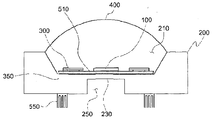
- FIG. 2 is a cross-sectional view showing an LED package according to a first embodiment of the present invention
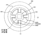
- FIG. 3 is a plan view of FIG.
- thermoelectric cooling device according to the first embodiment of the present invention is disposed
- FIG. 8 is a cross-sectional view showing a state in which the heat insulation member is installed according to the first embodiment of the present invention
- FIG. 9 is a cross-sectional view showing a heat insulating member according to a first embodiment of the present invention.
- thermoelectric cooling device 10 to 15 are plan views showing a state in which the thermoelectric cooling device according to the first embodiment of the present invention is disposed;
- FIG. 16 is a cross-sectional view showing a state in which an oxide film is formed according to a first embodiment of the present invention
- 17 is a cross-sectional view showing a cap-shaped encapsulant according to the first embodiment of the present invention
- FIG. 18 is a perspective view of an LED package according to a second embodiment of the present invention.
- 19 is a cross-sectional view showing a cap-shaped encapsulant according to a second embodiment of the present invention.
- thermoelectric semiconductor module 310 thermoelectric semiconductor module 310
- 310' p-type thermoelectric semiconductor
- thermoconductor 350, 350' electrode
- thermoelectric cooling device incorporating the thermoelectric cooling device according to a first embodiment of the present invention.
- FIG. 2 is a cross-sectional view showing the LED package according to the first embodiment of the present invention
- Figure 3 is a plan view of Figure 2
- the LED package in which the thermoelectric cooling device is installed according to the first embodiment of the present invention includes an LED (LED) device 100, a circuit board 200, a heat insulating member 230, and a heat insulating groove 250.
- the thermoelectric cooling element 300 may include an encapsulant 400 and a heat dissipation fin 500.
- the LED element 100 is mounted on the upper surface of the circuit board 200 and is electrically connected to a conductive circuit provided on the surface of the circuit board 200 through bonding means.
- the LED device 100 may be supplied with driving power through the circuit board 200.
- Light emitted from the LED device 100 may be converted into light of a different color by the phosphor contained in the encapsulant 400 to be described later.
- the light emitted from the blue LED device generating blue light may be emitted as white light through wavelength conversion by the phosphor contained in the encapsulant 400.
- the LED device 100 may be mounted on the upper surface of the circuit board 200.
- the LED device 100 forms the circuit board 200 in a planar shape and mounts it on the upper surface thereof, or forms a cavity 210 on the upper surface of the circuit board 200 as shown in FIG. Can be mounted
- the cavity 210 may be formed to be inclined from the upper surface of the circuit board 200 so that its inner wall decreases in radius from the top to the bottom in order to reflect the light emitted from the LED element 100 within a desired direction angle range. It is preferable that the inclined inner wall of the cavity 210 is formed of a metal material having excellent reflectivity, or the surface is metal-coated to form a reflective surface.
- thermoelectric cooling element 300 may install a horizontal thermoelectric cooling element 300 adjacent to the LED element 100. That is, the thermoelectric cooling element 300 is horizontally installed on the upper surface of the circuit board 200 adjacent to the LED element 100.
- the thermoelectric cooling device 300 serves as a cooling device that absorbs heat generated from the LED device 100 from one side and releases it to the other side by using a Peltier effect. That is, one end adjacent to the LED element 100 becomes a heat absorbing portion for absorbing heat, and the other end becomes a heat generating portion for emitting absorbed heat.
- the thermoelectric cooling element 300 may be configured by connecting the P-type thermoelectric semiconductor 310 and the N-type thermoelectric semiconductor 330 in series. In this case, the size of the P-type thermoconductor 310 and the N-type thermoconductor 330 may be minimized.
- the P-type thermoelectric semiconductor 310 and the N-type thermoelectric semiconductor 330 are energized by an electrode 350 provided on the upper surface of the circuit board 200.
- an insulating layer (not shown) is formed below the electrode 350 with the circuit board 200.
- thermoelectric cooling device 300 When the user wants to actively cool the heat generated by the LED device 100 using the thermoelectric cooling device 300, as illustrated in FIG. 3, the plurality of P-type thermoelectric semiconductors 310 and N-type thermoelectric semiconductors 330. ) Alternately horizontally installed, and the thermoelectric cooling device 300 in which the P-type thermoelectric semiconductor 310 and the N-type thermoelectric semiconductor 330 are connected in series is radially centered on the LED device 100. It may be disposed adjacent to the LED element 100 along the edge of the (100).
- thermoconductors 310 and N-type thermoconductors 330 are disposed adjacent to the LED elements 100 at positions opposing to the LED elements 100. can do.
- thermoelectric cooling device 300 including the P-type thermoelectric semiconductor 310, the N-type thermoelectric semiconductor 330, and the electrode 350 is formed around the LED device 100.
- a plurality of adjacent LED elements 100 may be installed along the edge of the 100.
- thermoelectric cooling elements 370 and 380 may be installed on the upper surface of the circuit board 200 to form a concentric circle around the LED element 100.
- a first thermoelectric cooling element 370 including a plurality of P-type thermoconductors, N-type thermoconductors, and electrodes may be disposed to be radially spaced apart from the LED element 100, and the LED element 100 may be disposed.
- a second thermoelectric cooling element 380 including a plurality of P-type thermoelectric semiconductors, N-type thermoelectric semiconductors, and electrodes may be disposed adjacent to a heat generating portion of the first thermoelectric cooling element 370.
- thermoelectric cooling elements such as a third thermoelectric cooling element adjacent to the second thermoelectric cooling element 380 and a fourth thermoelectric cooling element adjacent to the third thermoelectric cooling element may be sequentially installed in the same manner as described above.
- the first thermoelectric cooling element 370 disposed adjacent to the LED element 100 emits heat generated by the LED element 100 through the heat generating unit, and the second thermoelectric cooling element 380 is the first thermoelectric cooling element 370.
- the second thermoelectric cooling element 380 is the first thermoelectric cooling element 370.
- thermoelectric cooling device 300 may be configured by interconnecting the first thermoelectric cooling device and the second thermoelectric cooling device arranged in a concentric manner with respect to the LED device 100. have.
- an insulating groove 250 having a predetermined depth in the upper surface direction may be formed on the lower surface of the circuit board 200.
- the location of the insulating groove 250 is a lower surface of the circuit board 200 corresponding to the position of the LED device 100, the area of the bottom surface of the insulating groove 250 can be formed larger than the area of the LED device 100. have.
- Air in the insulation groove 250 is to perform a heat insulation function. As shown in FIG. 2 and FIG. 8, the heat insulating groove part 250 is for inducing heat conduction toward the heat absorbing part side of the thermoelectric cooling element 300 by blocking the heat conduction path to the lower portion of the circuit board 200.
- FIG 8 is a cross-sectional view showing a state in which the heat insulating member is installed according to the first embodiment of the present invention
- Figure 9 is a cross-sectional view showing a heat insulating member according to the first embodiment of the present invention.
- thermoelectric cooling element 300 schematically show a heat conduction path in which heat transferred from the LED element 100 to the circuit board 200 is guided to the thermoelectric cooling element 300 by the heat insulating groove 250. This is because the heat dissipation efficiency using the thermoelectric cooling element 300 to the outside than the heat dissipation to the outside through the circuit board 200 is greater.
- the circuit board 200 may be provided with a heat insulating member 230 in the lower portion of the mounted LED element 100. That is, the heat insulating member 230 may be installed on the upper surface of the circuit board 200 on which the LED element 100 is mounted.
- the heat insulating member 230 is formed smaller than the area of the LED element 100, the portion of the circuit board 200 that the heat of the LED element 100 is in contact with the LED element 100 around the heat insulating member 230 It is preferable to configure so as to easily conduct through the heat absorbing portion side of the thermoelectric cooling device (300).
- the heat insulating member 230 may be made of a porous material in order to reduce the thermal conductivity.
- FIG. 9 is a view showing an example of a heat insulating member 230 made of a porous material according to an embodiment of the present invention.
- the heat insulating member 230 stacks a plurality of silicon wafers 231 and bonds them with an oxide film 237, and the upper surface of the stacked silicon wafers 231 is disposed on an upper surface of the silicon wafer 231.
- the plurality of voids 235 are formed in the stacked silicon wafer 231 by etching (eg, wet etching) through the holes 233. It can manufacture by a method.
- Such a heat insulating member 230 of the porous material may use the heat insulating property of the air trapped in the cavity 235.
- a heat dissipation fin 500 may be further provided on the bottom surface of the circuit board 200.
- the heat dissipation fin 500 serves to discharge heat conducted to the circuit board 200 to the outside.
- the heat dissipation fins 500 may be installed over the entire lower surface of the circuit board 200.
- thermoelectric cooling element 300 a part of the heat emitted from the heat generating part of the thermoelectric cooling element 300 is transferred to the circuit board 200, and the thermoelectric part is formed by the heat insulating groove part 250 formed on the bottom surface of the circuit board 200. Part of the heat induced to the heat absorbing portion side of the cooling element 300 is moved along the circuit board 200 to the circuit board near the heat generating portion of the thermoelectric cooling element 300.
- thermoelectric cooling element 300 in which the heat generating part electrode is positioned is heated to a higher temperature than the other portion, so that the circuit board 200 corresponding to the electrode position of the thermoelectric cooling element 300 is formed.
- the heat radiation fins 550 only in the bottom position may be configured to increase the amount of heat radiation in this portion.
- the circuit board 200 may be generally formed of a silicon material, but may be formed of any one selected from a material consisting of aluminum, copper, gold, silver, and combinations having high thermal conductivity.
- a material having a high thermal conductivity By using a material having a high thermal conductivity, a large amount of heat emitted from the heat generating portion of the thermoelectric cooling element 300 is quickly conducted to the circuit board 200, and easily radiates the conducted heat to the outside to the LED element 100. Cooling efficiency can be increased.
- the heat dissipation fin 500 may also be formed of any one of aluminum, copper, gold, silver, and a combination thereof having high thermal conductivity, thereby increasing heat dissipation efficiency to the outside.
- the encapsulant 400 may be formed on the LED element 100 and the thermoelectric cooling element 300.
- the encapsulant 400 may fix the LED element 100 and the thermoelectric cooling element 300 to an upper portion of the circuit board 200, in particular, a bottom surface of the cavity 210.
- the encapsulant 400 may be a transparent resin such as a silicone resin, an epoxy resin, or a mixed resin thereof, and it is preferable to use a silicone resin to which phosphors and other mixtures are added.
- the encapsulant 400 may be configured to act as a lens.
- FIG. 10 is a cross-sectional view showing another example in which the heat insulation member and the heat insulation groove portion are installed according to the first embodiment of the present invention.
- a heat insulating member 230 may be widely installed at a position corresponding to the LED element 100 and the thermoelectric cooling element 300 mounted on the circuit board 200 among upper portions of the circuit board 200. Can be. That is, the heat insulating member 230 may be installed on the entire upper surface of the circuit board 200 on which the LED element 100 is mounted.
- the heat insulating member 230 is formed larger than the area of the LED element 100, the heat of the LED element 100 to the circuit board 200 in contact with the LED element 100 around the heat insulating member 230 Without facing, it may be configured to be easily conducted to the heat absorbing portion side of the thermoelectric cooling element (300).
- an insulating groove 250 having a predetermined depth in an upper surface direction may be formed on a lower surface of the circuit board 200.
- the insulation groove 250 may be formed in a groove shape on a lower surface of the circuit board 200 corresponding to the position of the insulation member 230 illustrated in FIG. 10. Air in the insulation groove 250 is to perform a heat insulation function.
- FIG. 11 is a cross-sectional view showing another example of the heat insulating member and the heat insulating groove.
- a heat insulating member 230 may be installed at a position corresponding to the LED element 100 and the thermoelectric cooling element 300 among the upper portions of the circuit board 200.
- the lower surface of the circuit board 200 may be formed with an insulating groove 250 having a predetermined depth in the upper surface direction.
- the heat insulating groove 250 is a lower surface of the circuit board 200 corresponding to the position of the LED element 100 shown in FIG. 11, but the area of the bottom surface of the heat insulating groove 250 is larger than the area of the LED element 100. It can form large.
- FIG. 12 is a cross-sectional view showing another example of the heat insulating member and the heat insulating groove.
- a heat insulating member 230 may be installed at a position corresponding to the LED element 100 among upper portions of the circuit board 200.
- the lower surface of the circuit board 200 may be formed with a heat insulating groove 250 having a predetermined depth in the upper surface direction.
- the insulation groove 250 may be formed on the lower surface of the circuit board 200 corresponding to the positions of the LED element 100 and the thermoelectric cooling element 300 illustrated in FIG. 12.
- the arrow shown in FIG. 12 schematically illustrates a heat conduction path in which heat transferred from the LED element 100 to the circuit board 200 is guided to the thermoelectric cooling element 300 by the heat insulating groove 250. This is because the heat dissipation efficiency using the thermoelectric cooling element 300 to the outside than the heat dissipation to the outside through the circuit board 200 is greater.
- FIG. 13 is a cross-sectional view showing another example of the heat insulating member and the heat insulating groove.
- a heat insulating member 230 may be installed at a position corresponding to the LED element 100 among upper portions of the circuit board 200.
- the insulating groove 250 may be formed on the lower surface of the circuit board 200 corresponding to the position of the LED element 100 and the thermoelectric cooling element 300 of the circuit board 200 as a whole.
- the insulating grooves 251, 252, and 253 may be formed at positions corresponding to the LED element 100 and the thermoelectric cooling element 300 among the upper portions of the circuit board 200. That is, the insulating grooves 251, 252, and 253 may be formed at positions corresponding to the LED element 100 and the thermoelectric cooling element 300 among the upper portions of the insulating grooves 250.
- the heat insulation members 230, 231, and 232 may be configured such that the heat of the LED element 100 may be increased in the vicinity of the heat insulation members 230, 231, and 232.
- the heat insulating grooves 250, 251, 252, and 253 block the heat conduction path to the lower portion of the circuit board 200 to induce heat conduction toward the heat absorbing portion side of the thermoelectric cooling element 300, whereby the heat insulating grooves ( Air in 250, 251, 252, and 253 may perform an adiabatic function.
- FIG. 14 and 15 are cross-sectional views showing another example of the heat insulating member and the heat insulating groove.
- a heat insulating member 230 may be installed at a position corresponding to the LED element 100 among upper portions of the circuit board 200.
- the insulating members 231 and 232 may be installed in the form of a partition wall between the LED element 100 and the thermoelectric cooling element 300 among the upper surfaces of the circuit board 200. Therefore, the LED element 100, the thermoelectric cooling element 300, and the heat insulating members 231 and 232 may be installed together on the upper surface of the circuit board 200.
- a plurality of heat insulating members 231 and 232 are installed in the form of partition walls. Referring to FIG.
- the insulating members 231 and 232 may be formed along the periphery of the P-type thermoconductor 310 and the N-type thermoconductor 330, and one side thereof may face the LED element 100. Can be.
- the heat insulating members 231 and 232 are elements for heat insulation of the heat generated from the LED device 100 and may be formed as a heat insulating coating layer.
- Insulating members 231 and 232 having a partition shape are formed between the LED element 100 and the thermoelectric cooling element 300, so that the heat of the LED element 100 is led around the insulating elements 231 and 232. It is preferable to configure such that it is easily conducted to the heat absorbing portion side of the thermoelectric cooling element 300 through the portion of the circuit board 200 in contact with 100.
- 16 is a cross-sectional view showing a state in which an oxide film is formed according to the first embodiment of the present invention.
- an insulating groove 250 having a predetermined depth in an upper surface direction may be formed on a lower surface of the circuit board 200.
- the insulation groove 250 may be formed on the bottom surface of the circuit board 200 corresponding to the position of the LED element 100 illustrated in FIG. 12.
- an oxide film 510 may be further formed on the upper surface of the circuit board 200.
- the oxide film 510 may be formed before the LED device 100 and the thermoelectric cooling device 300 are mounted on the upper surface of the circuit board 200. After the oxide film is formed and cured, or after the LED device 100 and the thermoelectric cooling device 300 are mounted, portions of the upper surface of the circuit board 200 corresponding to the oxide film 510 may be removed.
- a portion of the circuit board 200 is removed by the oxide film 510, and the oxide film 510 acts as the circuit board 200, thereby providing a path through which heat is transferred from the LED element 100 to the circuit board 200. Can be blocked beforehand. As a result, the circuit board 200 may be overheated, thereby heating the LED device 100, thereby eliminating the problem that the optical characteristics of the LED device 100 are degraded or the life thereof is shortened.
- 17 is a cross-sectional view showing a cap-shaped encapsulant according to the first embodiment of the present invention.
- a heat insulation member 230 is installed at a position corresponding to the LED element 100 among upper portions of the circuit board 200, and a bottom surface of the circuit board 200 corresponding to the position of the LED element 100 is provided. Insulating groove 250 having a predetermined depth in the upper direction may be formed.
- a cap 610 may be installed between the LED element 100, the thermoelectric cooling element 300, and the encapsulant 400.
- the cap 610 has the same curvature as the upper surface of the encapsulant 400 or has a different curvature.
- the interior between the LED device 100, the thermoelectric cooling device 300, and the cap 610 may be in a hollow state.
- the cap 610 may prevent the heat generated from the LED element 200 from being dispersed in the encapsulant 400 direction, and may rapidly absorb the heat from the thermoelectric cooling element 300.
- thermoelectric cooling device containing a thermoelectric cooling device according to a second embodiment of the present invention.
- FIG. 18 is a perspective view illustrating an LED package according to a second embodiment of the present invention.
- an LED package incorporating a thermoelectric cooling device may include an LED device 100 ′, a circuit board 200 ′, a thermoelectric cooling device 300 ′, and an encapsulant 400. '), May include a heat radiation fin (500').
- the LED device 100 ′ may be formed on the top surface of the circuit board 200 ′ in a planar shape.
- the LED element 100 ' is electrically connected to a conductive circuit provided on the surface of the circuit board 200' by bonding means. Since the LED element 100 'is the same as described in the first embodiment of the present invention, a detailed description thereof will be omitted.
- the LED element 100 ' is installed on the circuit board 200'.
- the circuit board 200 ' may be formed of a silicon material, but preferably, any one selected from aluminum, copper, gold, silver, and a combination of materials having high thermal conductivity may be used to generate heat generated from the LED device 100'. It can be easily delivered to the outside.
- circuit board 200 ′ is as described in the first embodiment of the present invention, a detailed description thereof will be omitted.
- the user may form the encapsulant 400 'on the circuit board 200'.
- the LED element 100 ′ and the thermoelectric cooling element 300 ′ to be described later are embedded in the encapsulant 400 ′ and fixed to the upper portion of the circuit board 200 ′ by the encapsulant 400 ′.
- thermoelectric cooling element 300 ′ may be installed vertically between the LED element 100 ′ and the circuit board 200 ′. That is, the thermoelectric cooling element 300 'is provided with electrodes 350' provided on the upper surface of the circuit board 200 'and the lower surface of the LED element 100', respectively, on the thermoelectric substrates 600 'and 601'. And a plurality of P-type thermoconductors 310 'and N-type thermoconductors 330' alternately connected in series by the electrodes 350 '.
- the P-type thermoelectric semiconductor 310 'and the N-type thermoelectric semiconductor 330' may be joined in series in a ⁇ -type.
- An insulating layer (not shown) is formed between the thermoelectric substrates 600 'and 601' and the electrode 350 '.
- thermoelectric cooling element 300 ' is an end portion absorbing heat at one end adjacent to the LED element 100', and the other end is a heat generating portion emitting the absorbed heat. Therefore, heat emitted from the LED element 100 'is actively absorbed by the heat absorbing portion of the thermoelectric cooling element 300' and is transferred to the circuit board 200 'through the heat generating portion.
- a heat dissipation fin 500' may be further installed on the bottom surface of the circuit board 200 '.
- the heat dissipation fin 500 may be formed of any one of aluminum, copper, gold, silver, and a combination thereof having high thermal conductivity, thereby increasing heat dissipation efficiency.
- 19 is a cross-sectional view showing a cap-shaped encapsulant according to a second embodiment of the present invention.
- a cap 610 ′ may be installed between the LED element 100 ′, the thermoelectric cooling element 300 ′, and the encapsulant 400 ′.
- the cap 610 ′ has the same curvature as the top surface of the encapsulant 400 ′ or has a different curvature.
- the interior between the LED element 100 'and the thermoelectric cooling element 300' and the cap 610 ' may be hollow.
- the cap 610 ′ may prevent the heat generated from the LED element 200 ′ from dispersing in the direction of the encapsulant 400 ′ as much as possible, and may allow the cap 610 ′ to be rapidly absorbed by the thermoelectric cooling element 300 ′.
Landscapes
- Led Device Packages (AREA)
- Cooling Or The Like Of Semiconductors Or Solid State Devices (AREA)
Abstract
열전냉각소자가 내장된 엘이디 패키지가 제공된다. 회로기판의 상면에는 엘이디(LED) 소자가 실장되며, 열전냉각소자는 엘이디 소자에 인접하여 회로기판의 상면에 수평되게 설치되며, 봉지재는 엘이디 소자 및 열전냉각소자의 상부에 형성될 수 있다.
Description
본 발명은 열전냉각소자가 내장된 엘이디 패키지에 관한 것으로서, 더욱 상
세하게는 열전냉각소자를 이용하여 엘이디 소자에서 발생하는 열을 능동적으로 외부로 방출할 수 있도록 하는 열전냉각소자가 내장된 엘이디 패키지에 관한 것이다.
엘이디(LED, light-emitting diode) 소자는 전력소모가 적기 때문에 디스플레이 장치, 실내외 조명, 자동차 헤드라이트 등 다양한 분야에서 광원으로 주목받고 있다. 엘이디 소자는 내부 저항 등에 의해 고온의 열이 발생하는데 이 열은 엘이디 소자의 자체 성능이나 수명에 큰 영향을 주기 때문에 방열 문제가 상당히 중요한 기술로 부각되고 있다.
종래의 엘이디 소자는 대개 실리콘 등의 플라스틱 소재의 인쇄회로기판(PCB)에 전극 패턴이 형성되고 엘이디 소자가 부착되어 구성되는데, PCB는 그 자체로 방열특성이 좋지 않아 엘이디 소자에서 발생한 열을 외부로 용이하게 방출하지 못한다. 따라서, 엘이디 소자가 과열되어 광특성이 저하되거나, 엘이디 소자의 수명이 단축되는 등의 문제점이 있었다.
이러한 문제점을 해결하기 위한 엘이디 소자 방열 방식으로 수동냉각 방식과 능동냉각 방식이 제안되어 있다. 수동냉각 방식의 일례는 대한민국 등록특허 제10-703218호에 개시되어 있는 데, 열전도 특성이 좋은 금속소재인 알루미늄을 엘이디 소자가 본딩되는 회로기판의 소재로 사용하고, 상기 알루미늄 기판에 양극산화막을 형성한 후, 복수의 기판 전극을 형성하고, 상기 기판 전극을 엘이디 소자와 전기적으로 연결하여 엘이디 패키지에 관한 것이다.
그러나 상기 종래기술은 금속소재인 알루미늄 기판은 열전도량의 한계 때문
에 엘이디 소자에서 발생하는 열을 충분히 방출하는데 어려움이 있다. 능동냉각 방식은 일례는 대한민국 특허공개 제2009-103263호에 개시되어 있는데, 도 1을 참조하여 그 구성을 설명하면 다음과 같다. 엘이디 소자로 구성되는 발광부(10)를 히트싱크(80)의 상부에 접착하고, 납땜(85)으로 히트싱크(80)의 하부에 난연성 절연고무(90)를 결합하고, 발광부(10)에 서 발생하는 열을 흡열하도록 상기 난연성 절연고무(90)의 하부에 전도성 물질인 구리판(40), 고열전도 절연체(30), 동 또는 알루미늄과 같은 메탈베이스(20)를 순차적으로 적층한다.
메탈베이스(20)의 하부에는 펠티에 효과를 이용하여 발광부(10)로부터 전달된 열을 상부에서 흡열하고 하부로 방출하도록 열전반도체(50)를 설치한다. 그리고 열전반도체(50)의 하부로 방출되는 열을 외부로 방출하기 위하여 전도성 물질인 전도체(60), 절연체(70), 난연성 절연고무(75)를 상기 열전반도체(50)의 하부로 순차적으로 적층한다. 그러나 이와 같이 발광부(10)에서 발생하는 열을 구리판(40), 고열전도 절연체(30)를 거쳐 메탈베이스(20)로 전달하는 경우 열전달 효율이 떨어지게 되어 발광부(10)에 대한 냉각효율이 전체적으로 저감되고, 열전반도체(50)의 상/하부에 전도성 물질을 적층함에 따라 엘이디 패키지의 크기가 커지는 문제점이 있다.
본 발명은 기존에 제안된 방법들의 상기와 같은 문제점들을 해결하기 위하여 제안된 것으로서, 엘이디 소자가 실장된 회로기판에 상기 엘이디 소자에 인접하게 수평형 열전냉각소자를 설치하거나, 회로기판과 상기 회로기판의 상부에 설치된 엘이디 소자 사이에 수직형 열전냉각소자를 설치하여 엘이디 소자에서 발생하는 열을 능동적으로 외부로 방출할 수 있는 열전냉각소자가 내장된 엘이디 패키지를 제공하는데 그 목적이 있다. 또한, 엘이디 소자에서 발생하는 열을 외부로 능동적으로 방출함으로써 엘이디 소자의 광특성 저하 및 수명 단축을 방지할 수 있는 열전냉각소자가 내장된 엘이디 패키지를 제공하는데 또 다른 목적이 있다.
본 발명의 일 실시예에 따르면, 상면에 엘이디(LED) 소자가 실장된 회로기판; 상기 엘이디 소자에 인접하여 상기 회로기판의 상면에 수평되게 설치하는 열전냉각소자; 및 상기 엘이디 소자 및 열전냉각소자의 상부에 형성된 봉지재를 포함하는 것을 특징으로 하는 열전냉각소자가 내장된 엘이디 패키지가 제공된다.
상기 회로기판은 상부에 캐비티(cavity)가 형성되고, 상기 엘이디 소자는 상기 캐비티의 저면에 실장되고, 상기 열전냉각소자는 상기 엘이디 소자에 인접하여 상기 캐비티의 저면에 설치될 수 있다.
상기 열전냉각소자는 복수의 P형 열전반도체 및 N형 열전반도체를 수평되게 교대로 설치하고, 직렬로 연결한 것을 특징으로 한다.
상기 P형 열전반도체 및 N형 열전반도체는 상기 엘이디 소자를 중심으로 방사형으로 배치될 수 있다.
상기 열전냉각소자는 상기 엘이디 소자를 중심으로 하여 동심원 형태를 이루도록 복수개 설치될 수 있다.
상기 엘이디 소자의 위치와 대응하는 회로기판의 하면 위치에 단열홈부가 형성될 수 있다.
상기 엘이디 소자 및 상기 열전냉각소자의 위치와 대응하는 회로기판의 하면 위치에 단열홈부가 형성될 수 있다.
상기 회로기판 내의 상부 중 상기 엘이디 소자와 상기 열전냉각소자의 사이에 대응하는 위치에 단열홈부가 형성될 수 있다.
상기 회로기판에는 상기 엘이디 소자의 하부에 단열부재가 설치될 수 있다.
상기 회로기판 내의 상부 중 상기 엘이디 소자 및 상기 열전냉각소자에 대응하는 위치에 단열부재가 설치될 수 있다.
상기 회로기판 내의 상면 중 상기 엘이디 소자와 상기 열전냉각소자의 사이에 격벽 형태로 단열부재가 설치될 수 있다.
상기 단열부재는 다공질 재질로 구성될 수 있다.
상기 단열부재는, 적층된 복수의 실리콘 웨이퍼의 상면에 형성된 다수의 홀과, 상기 홀과 연통되어 상기 실리콘 웨이퍼의 내부에 형성된 다수의 공동(void)을 구비할 수 있다.
상기 회로기판의 하면에는 방열핀이 더 설치될 수 있다.
상기 방열핀은 상기 열전냉각소자에서 발열하는 전극 위치에 대응하는 상기 회로기판의 하면 위치에 설치될 수 있다.
상기 회로기판의 상면에는 산화막이 더 형성될 수 있다.
상기 산화막이 형성된 후, 상기 회로기판의 상면 중 상기 산화막에 대응하는 부분이 제거될 수 있다.
상기 엘이디 소자 및 열전냉각소자와 상기 봉지재의 사이에 캡이 설치되며, 상기 엘이디 소자 및 열전냉각소자와 상기 캡 사이의 내부는 중공(hollowness) 상태일 수 있다.
상기 회로기판의 재질은 알루미늄, 구리, 금, 은 및 이의 조합에 의한 선택된 어느 하나로 구성될 수 있다.
한편, 본 발명의 다른 실시예에 따르면, 엘이디(LED) 소자가 상부에 설치된 회로기판; 상기 엘이디 소자와 상기 회로기판 사이에 설치되고, 복수의 P형 열전반도체 및 N형 열전반도체를 교대로 직렬로 연결한 열전냉각소자; 및 상기 엘이디 소자와 상기 열전냉각소자가 내재되게 상기 회로기판의 상부에 형성된 봉지재를 포함하는 것을 특징으로 하는 열전냉각소자가 내장된 엘이디 패키지가 제공된다.
상기 회로기판의 하면에는 방열핀이 더 설치될 수 있다.
상기 엘이디 소자 및 열전냉각소자와 상기 봉지재의 사이에 캡이 설치되며, 상기 엘이디 소자 및 열전냉각소자와 상기 캡 사이의 내부는 중공(hollowness) 상태일 수 있다.
본 발명에서 제안하고 있는 열전냉각소자가 내장된 엘이디 패키지에 따르면, 엘이디 소자가 실장된 회로기판에 상기 엘이디 소자에 인접하여 수평형 열전냉각소자를 설치하거나, 상기 엘이디 소자와 회로기판 사이에 수직형 열전냉각소자를 설치하여 엘이디 소자에서 발생하는 열을 능동적으로 외부로 방출함으로써 엘이디 소자의 광특성 저하 및 수명 단축을 방지할 수 있는 효과가 있다.
도 1은 종래기술에 따른 엘이디 패키지의 냉각구조를 나타내는 단면도,
도 2는 본 발명의 제1실시예에 따른 엘이디 패키지를 나타내는 단면도,
도 3은 도 2의 평면도,
도 4는 내지 도 7은 본 발명의 제1실시예에 따른 열전냉각소자가 배치된 상태를 나타내는 평면도,
도 8은 본 발명의 제1실시예에 따라 단열부재가 설치된 상태를 나타내는 단면도,
도 9는 본 발명의 제1실시예에 따른 단열부재를 나타내는 단면도,
도 10 내지 도 15는 본 발명의 제1실시예에 따른 열전냉각소자가 배치된 상태를 나타내는 평면도,
도 16은 본 발명의 제1실시예에 따라 산화막이 형성된 상태를 나타내는 단면도,
도 17은 본 발명의 제1실시예에 따른 캡 형태의 봉지재를 나타내는 단면도
도 18은 본 발명의 제2실시예에 따른 엘이디 패키지를 나타내는 사시도, 그리고,
도 19는 본 발명의 제2실시예에 따른 캡 형태의 봉지재를 나타내는 단면도이다.
*부호의 설명*
100, 100': 엘이디 소자 200, 200': 회로기판
210: 캐비티 230: 단열부재
231: 실리콘 웨이퍼 233: 홀
235: 공동 250: 단열홈부
300, 300': 열전반도체 모듈 310, 310': P형 열전반도체
330, 330': N형 열전반도체 350, 350': 전극
400, 400': 봉지재 500, 500': 방열핀
이상의 본 발명의 목적들, 다른 목적들, 특징들 및 이점들은 첨부된 도면과 관련된 이하의 바람직한 실시예들을 통해서 쉽게 이해될 것이다. 그러나 본 발명은 여기서 설명되는 실시예들에 한정되지 않고 다른 형태로 구체화될 수도 있다. 오히려, 여기서 소개되는 실시예들은 개시된 내용이 철저하고 완전해질 수 있도록 그리고 당업자에게 본 발명의 사상이 충분히 전달될 수 있도록 하기 위해 제공되는 것이다. 본 명세서에서, 어떤 구성요소가 다른 구성요소 상에 있다고 언급되는 경우에 그것은 다른 구성요소 상에 직접 형성될 수 있거나 또는 그들 사이에 제 3의 구성요소가 개재될 수도 있다는 것을 의미한다. 또한 도면들에 있어서, 구성요소들의 두께는 기술적 내용의 효과적인 설명을 위해 과장된 것이다.
본 명세서에서 사용된 용어는 실시예들을 설명하기 위한 것이며 본 발명을 제한하고자 하는 것은 아니다. 본 명세서에서, 단수형은 문구에서 특별히 언급하지 않는 한 복수형도 포함한다. 명세서에서 사용되는 '포함한다(comprises)' 및/또는 '포함하는(comprising)'은 언급된 구성요소는 하나 이상의 다른 구성요소의 존재 또는 추가를 배제하지 않는다.
이하, 도면을 참조하여 본 발명을 상세히 설명하도록 한다. 아래의 특정 실시예들을 기술하는데 있어서, 여러 가지의 특정적인 내용들은 발명을 더 구체적으로 설명하고 이해를 돕기 위해 작성되었다. 하지만 본 발명을 이해할 수 있을 정도로 이 분야의 지식을 갖고 있는 독자는 이러한 여러 가지의 특정적인 내용들이 없어도 사용될 수 있다는 것을 인지할 수 있다. 어떤 경우에는, 발명을 기술하는 데 있어서 흔히 알려졌으면서 발명과 크게 관련 없는 부분들은 본 발명을 설명하는 데 있어 별 이유 없이 혼돈이 오는 것을 막기 위해 기술하지 않음을 미리 언급해 둔다. 또한, 각 도면의 구성요소들에 참조번호를 부여함에 있어서, 동일한 구성요소들에 있어서는 비록 다른 도면상에 표시되더라도 동일한 번호를 가지도록 한다.
이하에서는 첨부된 도면들을 참조하여, 본 발명의 제1실시예에 따른 열전냉각소자가 내장된 엘이디 패키지에 대하여 상세하게 설명하기로 한다.
도 2는 본 발명의 제1실시예에 따른 엘이디 패키지를 나타내는 단면도이고, 도 3은 도 2의 평면도이고, 도 4는 내지 도 7 및 도 10 내지 도 15는 본 발명의 제1실시예에 따른 열전냉각소자가 배치된 상태를 나타내는 평면도이다.
도 2를 참조하면, 본 발명의 제1실시예에 따른 열전냉각소자가 내장된 엘이디 패키지는 엘이디(LED) 소자(100), 회로기판(200), 단열부재(230), 단열홈부(250), 열전냉각소자(300), 봉지재(400), 방열핀(500)을 포함할 수 있다.
도 2 및 도 3에서 도시된 바와 같이, 엘이디 소자(100)는 회로기판(200)의 상면에 실장되고, 본딩수단을 통해 회로기판(200)의 표면에 구비된 전도성 회로와 전기적으로 연결된다. 이때, 엘이디 소자(100)는 회로기판(200)을 통하여 구동전원을 공급받을 수 있다. 엘이디 소자(100)에서 출사되는 빛은 후술하게 될 봉지재(400)에 함유된 형광체에 의해 다른 색의 빛으로 변환될 수 있다. 가령, 청색광을 생성하는 청색 엘이디 소자에서 출사되는 빛은 봉지재(400)에 함유된 형광체에 의한 파장변환을 통해 백색광으로 출사될 수 있다.
회로기판(200)의 상면에는 엘이디 소자(100)가 실장될 수 있다. 엘이디 소자(100)는 회로기판(200)을 평면형으로 형성하여 그 상면에 실장하거나, 도 2에 도시된 것처럼 회로기판(200)의 상부에 캐비티(cavity)(210)를 형성하고, 그 저면에 실장할 수 있다.
이때, 캐비티(210)는 엘이디 소자(100)에서 나온 빛을 원하는 지향각 범위 내로 반사시키기 위해 그 내벽이 상부에서 하부로 갈수록 반경이 감소하도록 회로기판(200)의 상면으로부터 경사지게 형성될 수 있다. 캐비티(210)의 경사진 내벽을 반사성이 뛰어난 금속 재질로 형성하거나, 표면을 금속코팅하여 반사면으로 형성하는 것이 바람직하다.
열전냉각소자(300)는 엘이디 소자(100)에 인접하여 수평형 열전냉각소자(300)를 설치할 수 있다. 즉 열전냉각소자(300)를 엘이디 소자(100)에 인접하여 회로기판(200)의 상면에 수평으로 설치한다.
열전냉각소자(300)는 펠티에 효과를 이용하여 엘이디 소자(100)에서 발생하는 열을 일측에서 흡열하고 타측으로 방출시키는 냉각장치 역할을 한다. 즉 엘이디 소자(100)에 인접된 일단이 열을 흡수하는 흡열부가 되고, 타단은 흡수된 열을 방출하는 발열부가 된다.
열전냉각소자(300)는 P형 열전반도체(310) 및 N형 열전반도체(330)를 직렬로 연결하여 구성할 수 있다. 이때, P형 열전반도체(310) 및 N형 열전반도체(330)를 박막형태로 하여 그 크기를 최소화할 수 있다.
P형 열전반도체(310) 및 N형 열전반도체(330)는 회로기판(200)의 상면에 설치된 전극(350)에 의해 통전된다. 이때, 전극(350)의 하부에는 회로기판(200)과의 사이에 절연층(미도시)이 형성된다.
사용자가 엘이디 소자(100)에서 발생하는 열을 열전냉각소자(300)를 이용하여 능동냉각하고자 하는 경우, 도 3에서 도시한 바와 같이 복수의 P형 열전반도체(310)와 N형 열전반도체(330)를 수평하게 교대로 설치하고, 상기 P형 열전반도체(310)와 N형 열전반도체(330)를 직렬로 연결한 열전냉각소자(300)를 엘이디 소자(100)를 중심으로 방사형으로 상기 엘이디 소자(100)의 테두리를 따라 상기 엘이디 소자(100)에 인접하게 배치할 수 있다.
이때, 도 4에서 도시한 바와 같이, 복수의 P형 열전반도체(310)와 N형 열전반도체(330)를 엘이디 소자(100)를 기준으로 대향되는 위치에 상기 엘이디 소자(100)에 인접하게 배치할 수 있다.
한편, 도 5에서 도시한 바와 같이 P형 열전반도체(310)와 N형 열전반도체(330) 및 전극(350)을 구비한 열전냉각소자(300)를 엘이디 소자(100)를 중심으로 상기 엘이디 소자(100)의 테두리를 따라 상기 엘이디 소자(100)에 인접하여 복수개 설치할 수 있다.
또한, 도 6에서 도시한 바와 같이 엘이디 소자(100)를 중심으로 하여 동심원형태를 이루도록 복수의 열전냉각소자(370)(380)를 회로기판(200)의 상면에 설치할수 있다. 가령, 엘이디 소자(100)를 중심으로 반경방향으로 소정간격 이격되게 복수의 P형 열전반도체와 N형 열전반도체 및 전극을 구비한 제1열전냉각소자(370)를 배치하고, 상기 엘이디 소자(100)를 중심으로 상기 제1열전냉각소자(370)의 발열부에 인접하게 복수의 P형 열전반도체와 N형 열전반도체 및 전극을 구비한 제2열전냉각 소자(380)를 배치할 수 있다.
또한 상기와 같은 방식으로 제2열전냉각소자(380)에 인접하게 제3열전냉각소자, 제3열전냉각소자에 인접하게 제4열전냉각소자 등 복수의 열전냉각소자를 차례로 설치할 수 있다.
엘이디 소자(100)에 인접하게 설치한 제1열전냉각소자(370)는 엘이디 소자(100)에서 발생한 열을 발열부를 통해 방출하고, 제2열전냉각소자(380)는 제1열전냉각소자(370)에서 방출한 열을 흡수하여 발열부를 통해 외부로 방출함으로써 엘이디소자(100)에서 발생하는 열을 외부로 신속하게 전달할 수 있다.
또한, 도 7에서 도시한 바와 같이 엘이디 소자(100)를 중심으로 하여 동심원형태로 배치된 제1열전냉각소자와 제2열전냉각소자를 상호 연결하여 하나의 열전냉각소자(300)를 구성할 수 있다.
상기와 같이, 엘이디 소자(100)를 중심으로 전방향에서 엘이디 소자(100)를 효율적으로 능동냉각시킴으로써 열로 인한 엘이디 소자(100)의 광도 등의 광특성이 저하되는 것을 방지할 수 있을 뿐만 아니라, 엘이디 소자(100)의 수명이 단축되는 것을 방지할 수 있다.
또한, 도 2에서 도시한 바와 같이 회로기판(200)의 하면에는 상면 방향으로 소정깊이를 갖는 단열홈부(250)를 형성할 수 있다. 단열홈부(250)의 위치는 엘이디 소자(100)의 위치와 대응하는 회로기판(200)의 하면으로 하되, 단열홈부(250)의 저면의 면적을 엘이디 소자(100)의 면적보다 크게 형성할 수 있다.
상기 단열홈부(250) 내의 공기는 단열기능을 수행하게 된다. 도 2 및 도 8에서 도시한 바와 같이 단열홈부(250)는 회로기판(200)의 하부로의 열전도 경로를 차단하여 열전냉각소자(300)의 흡열부 측으로 열전도를 유도하기 위함이다.
도 8은 본 발명의 제1실시예에 따라 단열부재가 설치된 상태를 나타내는 단면도이고, 도 9는 본 발명의 제1실시예에 따른 단열부재를 나타내는 단면도이다.
도 2 및 도 8에 도시된 화살표는 엘이디 소자(100)에서 회로기판(200)으로 전달된 열이 단열홈부(250)에 의해 열전냉각소자(300) 측으로 유도되는 열전도 경로를 개략적으로 나타낸 것이다. 이와 같이 열전냉각소자(300)를 이용하여 외부로 열을 방출하는 것이 회로기판(200)을 통하여 외부로 열을 방출하는 것보다 방열효율이 크기 때문이다.
한편, 도 8을 참조하면, 회로기판(200)에는 실장된 엘이디 소자(100)의 하부에 단열부재(230)가 설치될 수 있다. 즉 엘이디 소자(100)가 실장되는 회로기판(200)의 상면에 단열부재(230)를 설치할 수 있다.
이때, 단열부재(230)는 엘이디 소자(100)의 면적보다 작게 형성하여, 엘이디 소자(100)의 열이 단열부재(230) 주변에서 엘이디 소자(100)와 접촉하고 있는 회로기판(200) 부분을 통해 열전냉각소자(300)의 흡열부 측으로 쉽게 전도되도록 구성하는 것이 바람직하다.
한편 단열부재(230)는 열전도율을 작게 하기 위하여 다공질 재질로 할 수 있다.
도 9는 본 발명의 실시예에 따른 다공질 재질로 이루어진 단열부재(230)의 일례를 도시한 도면이다.
도 9를 참조하면, 단열부재(230)은, 복수의 실리콘 웨이퍼(231)를 적층하여 산화막(237)으로 본딩하고, 적층된 실리콘 웨이퍼(231) 중 상부에 설치된 실리콘 웨이퍼(231)의 상면에 다수의 홀(233)을 형성한 후, 상기 홀(233)을 통하여 식각(예를들어, wet etching)하여 적층된 실리콘 웨이퍼(231)의 내부에 다수의 공동(void)(235)을 형성하는 방법으로 제조할 수 있다.
이와 같은 다공성재질의 단열부재(230)는 공동(235) 속에 갇힌 공기의 단열성을 이용할 수 있다.
또한, 도 2에서 도시한 바와 같이 회로기판(200)의 하면에는 방열핀(500)을 더 설치할 수 있다. 방열핀(500)은 회로기판(200)에 전도된 열을 외부로 방출하는 역할을 한다. 상기 방열핀(500)은 회로기판(200)의 하면 전체에 걸쳐 설치할 수 있다.
한편, 도 8에서 도시한 바와 같이 열전냉각소자(300)의 발열부에서 방출되는 열의 일부는 회로기판(200)에 전달되고, 회로기판(200)의 하면에 형성된 단열홈부(250)에 의해 열전냉각소자(300)의 흡열부 측으로 유도된 열의 일부가 회로기판(200)을 따라 열전냉각소자(300)의 발열부 부근의 회로기판으로 이동하게 된다.
따라서, 회로기판(200)에서 열전냉각소자(300)의 발열부 전극이 위치하는 부분이 다른 부분에 비하여 높은 온도로 가열되기 때문에 열전냉각소자(300)의 전극 위치에 대응하는 회로기판(200)의 하면 위치에만 방열핀(550)을 설치하여 이 부분의 방열량을 증가시키도록 구성할 수도 있다.
회로기판(200)은 통상 실리콘 재질로 형성될 수 있으나, 열전도율이 높은 알루미늄, 구리, 금, 은 및 이들을 조합으로 이루어진 재질 중 선택된 어느 하나로 구성할 수도 있다. 열전도율이 높은 재질을 사용함으로써 열전냉각소자(300)의 발열부에서 방출하는 많은 열량은 신속하게 회로기판(200)에 전도되고, 전도된 열을 용이하게 외부로 방출하여 엘이디 소자(100)에 대한 냉각효율을 증대시킬 수 있다. 이때, 방열핀(500)도 열전도율이 높은 알루미늄, 구리, 금, 은 및 이의 조합에 의한 어느 하나로 구성하여 외부로의 방열효율을 증대시킬 수 있다.
봉지재(400)는 엘이디 소자(100) 및 열전냉각소자(300)의 상부에 형성할 수 있다. 봉지재(400)에 의해 엘이디 소자(100) 및 열전냉각소자(300)를 회로기판(200)의 상부, 특히 캐비티(210)의 저면에 고정할 수 있다. 여기서 봉지재(400)는 실리콘수지, 에폭시수지 또는 그 혼합수지와 같은 투명수지가 사용될 수 있으며, 형광체와 기타 혼합물이 첨가된 실리콘수지를 사용하는 것이 바람직하다. 이러한 봉지재(400)는 렌즈역할을 하도록 구성할 수 있다.
도 10은 본 발명의 제1실시예에 따라 단열부재와 단열홈부가 설치된 다른 예를 나타내는 단면도이다.
도 10에 도시한 바와 같이, 회로기판(200) 내의 상부 중 회로기판(200)에 실장된 엘이디 소자(100) 및 열전냉각소자(300)에 대응하는 위치에 단열부재(230)가 넓게 설치될 수 있다. 즉, 엘이디 소자(100)가 실장되는 회로기판(200) 내의 상면 전체에 걸쳐 단열부재(230)가 설치될 수 있다.
따라서, 단열부재(230)는 엘이디 소자(100)의 면적보다 크게 형성되므로, 엘이디 소자(100)의 열이 단열부재(230) 주변에서 엘이디 소자(100)와 접촉하고 있는 회로기판(200)으로 향하지 않고, 열전냉각소자(300)의 흡열부 측으로 쉽게 전도되도록 구성될 수 있다.
또한, 도 10에 도시한 바와 같이, 회로기판(200)의 하면에는 상면 방향으로 소정깊이를 갖는 단열홈부(250)가 형성될 수 있다. 단열홈부(250)는, 도 10에 도시된 단열부재(230)의 위치와 대응하는 회로기판(200)의 하면에 홈 형태로 형성될 수 있다. 상기 단열홈부(250) 내의 공기는 단열기능을 수행하게 된다.
도 11은 단열부재와 단열홈부의 다른 예를 나타내는 단면도이다.
도 11을 참조하면, 회로기판(200) 내의 상부 중 엘이디 소자(100) 및 열전냉각소자(300)에 대응하는 위치에 단열부재(230)가 설치될 수 있다. 또한, 회로기판(200)의 하면에는 상면 방향으로 소정깊이를 갖는 단열홈부(250)가 형성될 수 있다. 단열홈부(250)는, 도 11에 도시된 엘이디 소자(100)의 위치와 대응하는 회로기판(200)의 하면으로 하되, 단열홈부(250)의 저면의 면적을 엘이디 소자(100)의 면적보다 크게 형성할 수 있다.
도 12는 단열부재와 단열홈부의 다른 예를 나타내는 단면도이다.
도 12를 참조하면, 회로기판(200) 내의 상부 중 엘이디 소자(100)에 대응하는 위치에 단열부재(230)가 설치될 수 있다. 또한, 회로기판(200)의 하면에는 상면 방향으로 소정깊이를 갖는 단열홈부(250)가 형성될 수 있다. 단열홈부(250)는, 도 12에 도시된 엘이디 소자(100)와 열전냉각소자(300)의 위치에 대응하는 회로기판(200)의 하면에 전체적으로 넓게 형성할 수 있다.
도 12에 도시된 화살표는 엘이디 소자(100)에서 회로기판(200)으로 전달된 열이 단열홈부(250)에 의해 열전냉각소자(300) 측으로 유도되는 열전도 경로를 개략적으로 나타낸 것이다. 이와 같이 열전냉각소자(300)를 이용하여 외부로 열을 방출하는 것이 회로기판(200)을 통하여 외부로 열을 방출하는 것보다 방열효율이 크기 때문이다.
도 13은 단열부재와 단열홈부의 다른 예를 나타내는 단면도이다.
도 13을 참조하면, 회로기판(200) 내의 상부 중 엘이디 소자(100)에 대응하는 위치에 단열부재(230)가 설치될 수 있다. 또한, 단열홈부(250)가 회로기판(200) 중 엘이디 소자(100)와 열전냉각소자(300)의 위치에 대응하는 회로기판(200)의 하면에 전체적으로 넓게 형성할 수 있다. 또한, 회로기판(200) 내의 상부 중 엘이디 소자(100)와 열전냉각소자(300)의 사이에 대응하는 위치에 단열홈부들(251, 252, 253)이 형성될 수 있다. 즉, 단열홈부들(251, 252, 253)은 또는 단열홈부(250)의 상부 중 엘이디 소자(100)와 열전냉각소자(300)의 사이에 대응하는 위치에 형성될 수 있다.
도 10 내지 도 13을 참조하여 상술한 실시예들에 의하면, 단열부재들(230, 231, 232)은, 엘이디 소자(100)의 열이 단열부재들(230, 231, 232) 주변에서 엘이디 소자(100)와 접촉하고 있는 회로기판(200) 부분을 통해 열전냉각소자(300)의 흡열부 측으로 쉽게 전도되도록 한다. 또한, 단열홈부들(250, 251, 252, 253)은 회로기판(200)의 하부로의 열전도 경로를 차단하여 열전냉각소자(300)의 흡열부 측으로 열전도를 유도하며, 이로써, 단열홈부들(250, 251, 252, 253) 내의 공기는 단열기능을 수행할 수 있다.
도 14 및 도 15는 단열부재와 단열홈부의 다른 예를 나타내는 단면도이다.
도 14 및 도 15를 참조하면, 회로기판(200) 내의 상부 중 엘이디 소자(100)에 대응하는 위치에 단열부재(230)가 설치될 수 있다. 또한, 회로기판(200) 내의 상면 중 엘이디 소자(100)와 열전냉각소자(300)의 사이에 격벽 형태로 단열부재들(231, 232)이 설치될 수 있다. 따라서, 엘이디 소자(100), 열전냉각소자(300) 및 단열부재들(231, 232)은 회로기판(200)의 상면에 함께 설치될 수 있다. 열전냉각소자(300)가 복수 개인 경우, 단열부재들(231, 232)은 격벽 형태로 복수 개 설치된다. 도 15를 참조하면, 단열부재들(231, 232)은 P형 열전반도체(310) 및 N형 열전반도체(330)의 외곽을 따라 형성될 수 있으며, 일측은 엘이디 소자(100)를 향하도록 형성될 수 있다. 단열부재들(231, 232)은 엘이디 소자(100)로부터 발생한 열의 단열을 위한 소자로서, 단열용 코팅층으로 형성될 수 있다.
격벽 형태의 단열부재들(231, 232)은 엘이디 소자(100)와 열전냉각소자(300) 사이에 형성되어, 엘이디 소자(100)의 열이 단열부재들(231, 232) 주변에서 엘이디 소자(100)와 접촉하고 있는 회로기판(200) 부분을 통해 열전냉각소자(300)의 흡열부 측으로 쉽게 전도되도록 구성하는 것이 바람직하다.
도 16은 본 발명의 제1실시예에 따라 산화막이 형성된 상태를 나타내는 단면도이다.
도 16을 참조하면, 회로기판(200)의 하면에는 상면 방향으로 소정깊이를 갖는 단열홈부(250)가 형성될 수 있다. 단열홈부(250)는, 도 12에 도시된 엘이디 소자(100)의 위치에 대응하는 회로기판(200)의 하면에 형성할 수 있다. 또한, 회로기판(200)의 상면에는 산화막(510)이 더 형성될 수 있다. 산화막(510)은 엘이디 소자(100) 및 열전냉각소자(300)가 회로기판(200)의 상면에 실장되기 이전에 형성될 수 있다. 산화막이 형성되어 경화된 후, 또는 엘이디 소자(100)와 열전냉각소자(300)가 실장된 후, 회로기판(200)의 상면 중 산화막(510)에 대응하는 부분은 제거될 수 있다.
산화막(510)에 의해 회로기판(200)의 일부를 제거하고, 산화막(510)이 회로기판(200)의 역할을 대행함으로써 엘이디 소자(100)에서 회로기판(200)으로 열이 전달되는 경로를 미연에 차단할 수 있다. 이로써, 회로기판(200)이 과열되어 엘이디 소자(100)가 가열되며, 그로 인해 엘이디 소자(100)의 광특성이 저하되거나 수명이 단축되는 문제를 해소할 수 있다.
도 17은 본 발명의 제1실시예에 따른 캡 형태의 봉지재를 나타내는 단면도이다.
도 17을 참조하면, 회로기판(200) 내의 상부 중 엘이디 소자(100)에 대응하는 위치에 단열부재(230)가 설치되고, 엘이디 소자(100)의 위치에 대응하는 회로기판(200)의 하면에는 상면 방향으로 소정깊이를 갖는 단열홈부(250)가 형성될 수 있다. 또한, 엘이디 소자(100) 및 열전냉각소자(300)와 봉지재(400)의 사이에 캡(610)이 설치될 수 있다.
캡(610)은 봉지재(400)의 상면과 동일한 굴곡을 갖거나 다른 굴곡을 갖는다. 엘이디 소자(100) 및 열전냉각소자(300)와 캡(610) 사이의 내부는 중공(hollowness) 상태일 수 있다. 캡(610)은 엘이디 소자(200)로부터 발생한 열이 봉지재(400) 방향으로 분산되는 것을 방지하고, 열전냉각소자(300)로 보다 빠르게 흡열되도록 할 수 있다.
이하에서는 첨부된 도면들을 참조하여, 본 발명의 제2실시예에 따른 열전냉각소자가 내장된 엘이디 패키지에 대하여 상세하게 설명하기로 한다.
도 18은 본 발명의 제2실시예에 따른 엘이디 패키지를 나타내는 사시도이다.
도 18을 참고하면, 본 발명의 제2실시예에 따른 열전냉각소자가 내장된 엘이디 패키지는 엘이디 소자(100'), 회로기판(200'), 열전냉각소자(300'), 봉지재(400'), 방열핀(500')을 포함할 수 있다.
엘이디 소자(100')는 회로기판(200')을 평면형으로 형성하여 그 상면에 실장할 수 있다. 또한, 엘이디 소자(100')는 본딩수단에 의해 회로기판(200')의 표면에 구비된 전도성 회로와 전기적으로 연결된다. 이하 엘이디 소자(100')는 상기한 본 발명의 제1실시예에서 설명한 바와 같으므로 이에 대한 상세한 설명은 생략하기로 한다.
회로기판(200')의 상부에 엘이디 소자(100')를 설치한다. 회로기판(200')은 실리콘 재질로 형성할 수 있으나, 바람직하게는 열전도율이 높은 알루미늄, 구리, 금, 은 및 이들을 조합한 재질 중 선택된 어느 하나로 구성하여 엘이디 소자(100')에서 발생하는 열을 용이하게 외부로 전달할 수 있다.
이하 회로기판(200')은 상기한 본 발명의 제1실시예에서 설명한 바와 같으므로 이에 대한 상세한 설명은 생략하기로 한다.
사용자는 봉지재(400')를 회로기판(200')의 상부에 형성할 수 있다. 엘이디 소자(100')와 후술할 열전냉각소자(300')는 봉지재(400')에 내재되고, 봉지재(400')에 의해 회로기판(200')의 상부에 고정된다.
이하 봉지재(400')는 상기한 본 발명의 제1실시예에서 설명한 바와 같으므로 이에 대한 상세한 설명은 생략하기로 한다.
열전냉각소자(300')는 엘이디 소자(100')와 회로기판(200') 사이에 수직형으로 설치할 수 있다. 즉, 열전냉각소자(300')는 회로기판(200')의 상면 및 엘이디 소자(100')의 하면에 각각 배치된 열전소자기판(600')(601')에 설치한 전극(350')과, 상기 전극(350')에 의해 직렬로 교대로 연결된 복수의 P형 열전반도체(310') 및 N형 열전반도체(330')를 구비할 수 있다. 여기서 P형 열전반도체(310') 및 N형 열전반도체(330')는 직렬로 π형으로 접합할 수 있다. 그리고 열전소자기판(600')(601')와 전극(350')의 사이에는 절연층(미도시)을 형성한다.
여기서, 열전냉각소자(300')는 엘이디 소자(100')에 인접한 일단이 열을 흡수하는 흡열부가 되고, 타단은 흡수된 열을 방출하는 발열부가 된다. 따라서, 엘이디소자(100')에서 방출되는 열은 열전냉각소자(300')의 흡열부에서 능동적으로 흡수되고, 발열부를 통하여 회로기판(200')으로 전달된다.
회로기판(200')에 전달된 열을 외부로 용이하게 방출하기 위하여 회로기판(200')의 하면에는 방열핀(500')을 더 설치할 수 있다. 이때, 방열핀(500)을 열전도율이 높은 알루미늄, 구리, 금, 은 및 이의 조합에 의한 어느 하나로 구성하여 방열효율을 증대시킬 수 있다.
이하, 방열핀(500')은 상기한 본 발명의 제1실시예에서 설명한 바와 같으므로 이에 대한 상세한 설명은 생략하기로 한다.
도 19는 본 발명의 제2실시예에 따른 캡 형태의 봉지재를 나타내는 단면도이다.
도 19를 참조하면, 엘이디 소자(100') 및 열전냉각소자(300')와 봉지재(400')의 사이에 캡(610')이 설치될 수 있다. 캡(610')은 봉지재(400')의 상면과 동일한 굴곡을 갖거나 다른 굴곡을 갖는다. 엘이디 소자(100') 및 열전냉각소자(300')와 캡(610') 사이의 내부는 중공 상태일 수 있다. 캡(610')은 엘이디 소자(200')로부터 발생한 열이 봉지재(400') 방향으로 분산되는 것을 최대한 방지하고, 열전냉각소자(300')에 의해 보다 빠르게 흡열되도록 할 수 있다.
상기와 같이 본 발명은 비록 한정된 실시예와 도면에 의해 설명되었으나, 본 발명은 상기의 실시예에 한정되는 것은 아니며, 본 발명이 속하는 분야에서 통상의 지식을 가진 자라면 이러한 기재로부터 다양한 수정 및 변형이 가능하다. 그러므로, 본 발명의 범위는 설명된 실시예에 국한되어 정해져서는 아니 되며, 후술하는 특허청구범위뿐 아니라 이 특허청구범위와 균등한 것들에 의해 정해져야 한다.
Claims (22)
- 상면에 엘이디(LED) 소자가 실장된 회로기판;상기 엘이디 소자에 인접하여 상기 회로기판의 상면에 수평되게 설치하는 열전냉각소자; 및상기 엘이디 소자 및 열전냉각소자의 상부에 형성된 봉지재를 포함하는 것을 특징으로 하는 열전냉각소자가 내장된 엘이디 패키지.
- 제1항에 있어서,상기 회로기판은 상부에 캐비티(cavity)가 형성되고, 상기 엘이디 소자는 상기 캐비티의 저면에 실장되고, 상기 열전냉각소자는 상기 엘이디 소자에 인접하여 상기 캐비티의 저면에 설치된 것을 특징으로 하는 열전냉각소자가 내장된 엘이디 패키지.
- 제1항에 있어서,상기 열전냉각소자는 복수의 P형 열전반도체 및 N형 열전반도체를 수평되게 교대로 설치하고, 직렬로 연결한 것을 특징으로 하는 열전냉각소자가 내장된 엘이디 패키지.
- 제3항에 있어서,상기 P형 열전반도체 및 N형 열전반도체는 상기 엘이디 소자를 중심으로 방사형으로 배치된 것을 특징으로 하는 열전냉각소자가 내장된 엘이디 패키지.
- 제4항에 있어서,상기 열전냉각소자는 상기 엘이디 소자를 중심으로 하여 동심원 형태를 이루도록 복수개 설치된 것을 특징으로 하는 열전냉각소자가 내장된 엘이디 패키지.
- 제1항에 있어서,상기 엘이디 소자의 위치와 대응하는 회로기판의 하면 위치에 단열홈부가 형성된 것을 특징으로 하는 열전냉각소자가 내장된 엘이디 패키지.
- 제1항에 있어서,상기 엘이디 소자 및 상기 열전냉각소자의 위치와 대응하는 회로기판의 하면 위치에 단열홈부가 형성된 것을 특징으로 하는 열전냉각소자가 내장된 엘이디 패키지.
- 제1항에 있어서,상기 회로기판 내의 상부 중 상기 엘이디 소자와 상기 열전냉각소자의 사이에 대응하는 위치에 단열홈부가 형성된 것을 특징으로 하는 열전냉각소자가 내장된 엘이디 패키지.
- 제1항에 있어서,상기 회로기판에는 상기 엘이디 소자의 하부에 단열부재가 설치된 것을 특징으로 하는 열전냉각소자가 내장된 엘이디 패키지.
- 제1항에 있어서,상기 회로기판 내의 상부 중 상기 엘이디 소자 및 상기 열전냉각소자에 대응하는 위치에 단열부재가 설치된 것을 특징으로 하는 열전냉각소자가 내장된 엘이디 패키지.
- 제1항에 있어서,상기 회로기판 내의 상면 중 상기 엘이디 소자와 상기 열전냉각소자의 사이에 격벽 형태로 단열부재가 설치된 것을 특징으로 하는 열전냉각소자가 내장된 엘이디 패키지.
- 제9항 내지 제11항 중 어느 한 항에 있어서,상기 단열부재는 다공질 재질로 구성된 것을 특징으로 하는 열전냉각소자가 내장된 엘이디 패키지.
- 제9항 내지 제11항 중 어느 한 항에 있어서,상기 단열부재는, 적층된 복수의 실리콘 웨이퍼의 상면에 형성된 다수의 홀과, 상기 홀과 연통되어 상기 실리콘 웨이퍼의 내부에 형성된 다수의 공동(void)을 구비하는 것을 특징으로 하는 열전냉각소자가 내장된 엘이디 패키지.
- 제1항에 있어서,상기 회로기판의 하면에는 방열핀이 더 설치된 것을 특징으로 하는 열전냉각소자가 내장된 엘이디 패키지.
- 제14항에 있어서,상기 방열핀은 상기 열전냉각소자에서 발열하는 전극 위치에 대응하는 상기 회로기판의 하면 위치에 설치된 것을 특징으로 하는 열전냉각소자가 내장된 엘이디 패키지.
- 제1항에 있어서,상기 회로기판의 상면에는 산화막이 더 형성된 것을 특징으로 하는 열전냉각소자가 내장된 엘이디 패키지.
- 제16항에 있어서,상기 산화막이 형성된 후, 상기 회로기판의 상면 중 상기 산화막에 대응하는 부분이 제거된 것을 특징으로 하는 열전냉각소자가 내장된 엘이디 패키지.
- 제1항에 있어서,상기 엘이디 소자 및 열전냉각소자와 상기 봉지재의 사이에 캡이 설치되며, 상기 엘이디 소자 및 열전냉각소자와 상기 캡 사이의 내부는 중공(hollowness) 상태인 것을 특징으로 하는 열전냉각소자가 내장된 엘이디 패키지.
- 제1항에 있어서,상기 회로기판의 재질은 알루미늄, 구리, 금, 은 및 이의 조합에 의한 선택된 어느 하나로 구성된 것을 특징으로 하는 열전냉각소자가 내장된 엘이디 패키지.
- 엘이디(LED) 소자가 상부에 설치된 회로기판;상기 엘이디 소자와 상기 회로기판 사이에 설치되고, 복수의 P형 열전반도체 및 N형 열전반도체를 교대로 직렬로 연결한 열전냉각소자; 및상기 엘이디 소자와 상기 열전냉각소자가 내재되게 상기 회로기판의 상부에 형성된 봉지재를 포함하는 것을 특징으로 하는 열전냉각소자가 내장된 엘이디 패키지.
- 제20항에 있어서,상기 회로기판의 하면에는 방열핀이 더 설치된 것을 특징으로 하는 열전냉각소자가 내장된 엘이디 패키지.
- 제20항에 있어서,상기 엘이디 소자 및 열전냉각소자와 상기 봉지재의 사이에 캡이 설치되며, 상기 엘이디 소자 및 열전냉각소자와 상기 캡 사이의 내부는 중공(hollowness) 상태인 것을 특징으로 하는 열전냉각소자가 내장된 엘이디 패키지.
Applications Claiming Priority (2)
| Application Number | Priority Date | Filing Date | Title |
|---|---|---|---|
| KR1020100034906A KR101004746B1 (ko) | 2010-04-15 | 2010-04-15 | 열전냉각소자가 내장된 엘이디 패키지 |
| KR10-2010-0034906 | 2010-04-15 |
Publications (1)
| Publication Number | Publication Date |
|---|---|
| WO2011129514A1 true WO2011129514A1 (ko) | 2011-10-20 |
Family
ID=43615641
Family Applications (1)
| Application Number | Title | Priority Date | Filing Date |
|---|---|---|---|
| PCT/KR2010/009132 Ceased WO2011129514A1 (ko) | 2010-04-15 | 2010-12-21 | 열전냉각소자가 내장된 엘이디 패키지 |
Country Status (2)
| Country | Link |
|---|---|
| KR (1) | KR101004746B1 (ko) |
| WO (1) | WO2011129514A1 (ko) |
Families Citing this family (3)
| Publication number | Priority date | Publication date | Assignee | Title |
|---|---|---|---|---|
| KR101064870B1 (ko) | 2010-12-21 | 2011-09-15 | 한국기계연구원 | 열전냉각기능을 가지는 엘이디 패키지 |
| EP2790474B1 (en) * | 2013-04-09 | 2016-03-16 | Harman Becker Automotive Systems GmbH | Thermoelectric cooler/heater integrated in printed circuit board |
| KR101793595B1 (ko) * | 2015-09-25 | 2017-11-06 | 재단법인대구경북과학기술원 | 태양열과 지열의 온도 차를 이용한 자가발전 조명장치 |
Citations (6)
| Publication number | Priority date | Publication date | Assignee | Title |
|---|---|---|---|---|
| KR20060061435A (ko) * | 2004-12-02 | 2006-06-08 | 서울반도체 주식회사 | 발광 다이오드 패키지 |
| US20060179849A1 (en) * | 2005-02-14 | 2006-08-17 | Abramov Vladimir S | Peltier based heat transfer systems |
| JP2006294782A (ja) * | 2005-04-08 | 2006-10-26 | Hitachi Ltd | 半導体光源装置 |
| JP2007066696A (ja) * | 2005-08-31 | 2007-03-15 | Matsushita Electric Ind Co Ltd | 照明装置 |
| JP2007150329A (ja) * | 2005-11-28 | 2007-06-14 | Visteon Global Technologies Inc | 集積熱電チップを有する多層発光素子 |
| KR20090029341A (ko) * | 2007-09-18 | 2009-03-23 | 주식회사 세명반도체 | 냉각기능을 갖는 고휘도 발광다이오드용 조명수단 |
-
2010
- 2010-04-15 KR KR1020100034906A patent/KR101004746B1/ko active Active
- 2010-12-21 WO PCT/KR2010/009132 patent/WO2011129514A1/ko not_active Ceased
Patent Citations (6)
| Publication number | Priority date | Publication date | Assignee | Title |
|---|---|---|---|---|
| KR20060061435A (ko) * | 2004-12-02 | 2006-06-08 | 서울반도체 주식회사 | 발광 다이오드 패키지 |
| US20060179849A1 (en) * | 2005-02-14 | 2006-08-17 | Abramov Vladimir S | Peltier based heat transfer systems |
| JP2006294782A (ja) * | 2005-04-08 | 2006-10-26 | Hitachi Ltd | 半導体光源装置 |
| JP2007066696A (ja) * | 2005-08-31 | 2007-03-15 | Matsushita Electric Ind Co Ltd | 照明装置 |
| JP2007150329A (ja) * | 2005-11-28 | 2007-06-14 | Visteon Global Technologies Inc | 集積熱電チップを有する多層発光素子 |
| KR20090029341A (ko) * | 2007-09-18 | 2009-03-23 | 주식회사 세명반도체 | 냉각기능을 갖는 고휘도 발광다이오드용 조명수단 |
Also Published As
| Publication number | Publication date |
|---|---|
| KR101004746B1 (ko) | 2011-01-03 |
Similar Documents
| Publication | Publication Date | Title |
|---|---|---|
| KR101472403B1 (ko) | 발광소자 모듈 | |
| WO2013147504A1 (en) | Lighting device and method for manufacturing the same | |
| WO2011002208A2 (ko) | 발광 다이오드 패키지 | |
| WO2009157664A2 (ko) | 반도체 소자 패키지 | |
| WO2011159076A2 (ko) | 열전대를 이용한 고출력 광소자 가로등 | |
| WO2013073897A2 (ko) | 발광소자 패키지 및 이를 구비하는 백라이트 유닛 | |
| WO2013115439A1 (ko) | 히트싱크 및 이를 포함하는 엘이디 조명장치 | |
| WO2014010778A1 (ko) | 광 반도체 조명장치 | |
| CN101532657A (zh) | 照明装置 | |
| WO2012134079A2 (ko) | 엘이디 램프 | |
| WO2011049374A2 (ko) | 발광소자 및 이를 이용한 라이트 유닛 | |
| WO2011159077A2 (ko) | 열전대를 이용한 매립형 광소자 패키지 모듈 | |
| WO2014168379A1 (ko) | 이중실링된 방수용 투광등 및 그 방법 | |
| WO2010147271A1 (ko) | Led어레이모듈 및 그 제조방법 | |
| WO2011040671A1 (ko) | 발광다이오드 조명기구 | |
| WO2010074371A1 (ko) | 칩온보드형 발광 다이오드 패키지 및 그것의 제조 방법 | |
| WO2014142396A1 (ko) | 방열성능을 향상하고 누설전류를 방지하기 위한 금속회로를 장착한 고광력 led 광원 구조체 | |
| WO2012161380A1 (en) | Lighting apparatus | |
| WO2012036465A2 (ko) | 방열특성이 향상된 고광력 led 광원 구조체 | |
| WO2013032239A1 (en) | Lighting device | |
| WO2013036061A1 (en) | Lighting device | |
| WO2011129514A1 (ko) | 열전냉각소자가 내장된 엘이디 패키지 | |
| WO2017155354A1 (ko) | 조명 장치 | |
| WO2013027998A2 (ko) | 발광 소자 패키지, 이를 포함하는 조명 장치 및 조명 시스템 | |
| WO2014084693A1 (ko) | 발광 다이오드 및 그것을 제조하는 방법 |
Legal Events
| Date | Code | Title | Description |
|---|---|---|---|
| 121 | Ep: the epo has been informed by wipo that ep was designated in this application |
Ref document number: 10849918 Country of ref document: EP Kind code of ref document: A1 |
|
| NENP | Non-entry into the national phase |
Ref country code: DE |
|
| 122 | Ep: pct application non-entry in european phase |
Ref document number: 10849918 Country of ref document: EP Kind code of ref document: A1 |