WO2011125998A1 - 電子機器 - Google Patents
電子機器 Download PDFInfo
- Publication number
- WO2011125998A1 WO2011125998A1 PCT/JP2011/058575 JP2011058575W WO2011125998A1 WO 2011125998 A1 WO2011125998 A1 WO 2011125998A1 JP 2011058575 W JP2011058575 W JP 2011058575W WO 2011125998 A1 WO2011125998 A1 WO 2011125998A1
- Authority
- WO
- WIPO (PCT)
- Prior art keywords
- terminal
- usb
- connector
- switch
- analog
- Prior art date
- Legal status (The legal status is an assumption and is not a legal conclusion. Google has not performed a legal analysis and makes no representation as to the accuracy of the status listed.)
- Ceased
Links
Images




Classifications
-
- G—PHYSICS
- G06—COMPUTING OR CALCULATING; COUNTING
- G06F—ELECTRIC DIGITAL DATA PROCESSING
- G06F13/00—Interconnection of, or transfer of information or other signals between, memories, input/output devices or central processing units
- G06F13/38—Information transfer, e.g. on bus
- G06F13/40—Bus structure
- G06F13/4004—Coupling between buses
- G06F13/4022—Coupling between buses using switching circuits, e.g. switching matrix, connection or expansion network
-
- G—PHYSICS
- G06—COMPUTING OR CALCULATING; COUNTING
- G06F—ELECTRIC DIGITAL DATA PROCESSING
- G06F2213/00—Indexing scheme relating to interconnection of, or transfer of information or other signals between, memories, input/output devices or central processing units
- G06F2213/0042—Universal serial bus [USB]
Definitions
- This invention relates to an electronic device, and more particularly to an electronic device capable of outputting two types of signals, analog or digital, to the outside.
- Patent Document 1 discloses an apparatus having an apparatus connector including an input terminal for inputting an external control signal, an analog output terminal for outputting an analog signal, and a digital output terminal for outputting a digital signal.
- an electric apparatus including an analog input terminal for inputting an analog signal output from a terminal and a digital input terminal for inputting a digital signal output from the digital output terminal.
- JP 2006-293440 A JP 2006-293440 A
- the present invention has been made to solve the above-described problems, and one of the objects of the present invention is to provide an electronic apparatus with a reduced number of connectors.
- an electronic device can be connected to an analog cable that can input an analog signal and a digital device that can be connected to a digital device that can input and output a digital signal.
- a connector that can be connected to one of the cables, an analog circuit that outputs an analog signal, a digital circuit that inputs and outputs a digital signal, and a switching means that connects the connector to either the analog circuit or the digital circuit And comprising.
- the connector is connected to one of the analog circuit and the USB circuit, so that one of the analog signal and the USB signal can be output from one connector.
- an electronic device with a reduced number of connectors can be provided.
- the connector has at least an ID terminal, a GND terminal, and a data communication terminal
- the analog cable connects the ID terminal and the GND terminal
- the USB cable opens the ID terminal and is switched.
- the means includes pull-up means for pulling up the ID terminal to a predetermined voltage, and detection means for detecting the voltage of the ID terminal.
- the ID terminal when the analog cable is connected to the connector, the ID terminal is grounded, and when the USB cable is connected to the connector, the ID terminal is pulled up to a predetermined voltage. For this reason, it can be detected that an analog cable is connected to the connector.
- the switching means has a dynamic range limited to a predetermined range on the plus side, is provided between the connector and the USB circuit, and is connected between the data communication terminal of the connector and the USB circuit.
- a first connector switch that switches between the two, a dynamic range is limited to a predetermined range on the plus side, provided between the connector and the analog circuit, and a connection state and a non-connection state for connecting the data communication terminal of the connector and the analog circuit
- a second connector switch for switching to any one of the above, a control means for controlling the first connector switch and the second connector switch, and a capacitor connected in series between the second connector switch and the connector, the control means comprising: While the predetermined voltage is detected by the detection means and the detection means, the first connector switch Switch control means for setting the second connector switch to the connected state and the second connector switch to the disconnected state while the second connector switch is disconnected and the predetermined voltage is not detected by the detecting means. And including.
- the capacitor since the capacitor is connected in series between the analog circuit and the connector, an analog signal from which the DC component of the analog signal output from the analog circuit is removed can be output from the connector.
- the capacitor since the capacitor is connected between the second connector switch and the connector, the analog signal before removing the DC component is input to the second connector switch, so the dynamic range is limited to a predetermined range on the plus side.
- a second connector switch can be used.
- the data communication terminal includes a first data communication terminal and a second data communication terminal
- the analog circuit has a video signal output terminal and an audio signal output terminal
- the analog circuit is The video signal is output from the video signal output terminal
- the audio signal is output from the audio signal output terminal
- the first data communication terminal is connected to the video signal output terminal
- the second data communication terminal is the audio signal output terminal.
- the capacitor is connected between the second data communication terminal and the audio signal output terminal.
- the switching means is provided between the connector, the analog circuit, and the USB circuit, and connects the data communication terminal of the connector to one of the analog circuit and the USB circuit, and control for controlling the connector switch.
- the control means outputs to the connector switch an instruction to connect the data communication terminal of the connector to the USB circuit while the predetermined voltage is detected by the detection means and the detection means.
- Switching control means for outputting, to the connector switch, an instruction to connect the data communication terminal of the connector to the analog circuit.
- the connector has at least an ID terminal, a GND terminal, and a data communication terminal
- the analog device connected to the analog cable grounds the ID terminal with the analog cable connected to the connector, and the digital cable.
- Open the ID terminal and the switching means includes pull-up means for pulling up the ID terminal to a predetermined voltage, and detection means for detecting the voltage of the ID terminal.
- the switching means includes a changeover switch for connecting the ID terminal to an analog circuit after the detection means detects a voltage of the ID terminal smaller than a predetermined value.
- the switching means is provided between the connector and the analog circuit and the digital circuit, and connects the data communication terminal of the connector to either one of the analog circuit or the digital circuit, and a control for controlling the connector switch.
- the control means is a connector switch that instructs the connector switch to connect the data communication terminal of the connector to the digital circuit before the detection means detects a voltage at the ID terminal smaller than a predetermined value by the detection means.
- switching control means for outputting an instruction to connect the data communication terminal of the connector to the analog circuit to the connector switch after the detection means detects the voltage of the ID terminal smaller than a predetermined value.
- FIG. 1 is a block diagram showing an outline of the configuration of a video camera according to one embodiment.
- a digital video camera 10 includes a central processing unit (CPU) 11 that controls the entire digital video camera 10, and a ROM (Read Only Memory) 13 that stores a program to be executed by the CPU 11.
- CPU central processing unit
- ROM Read Only Memory
- Image sensor 15 operation unit 17, microphone 21, analog / digital conversion units (A / D) 19, 23, memory control unit 25, SDRAM (Synchronous Dynamic Random Access Memory) 27, and liquid crystal display device (LCD) 31, LCD driver 29, JPEG (Joint Photographic Experts Group) -CODEC33, MPEG (Moving Picture Experts Group) -CODEC35, large capacity It includes a hard disk drive (HDD) 37 as an apparatus, the input-output circuit 41, a USB socket 43.
- HDD hard disk drive
- CPU 11 memory control unit 25, JPEG-CODEC 33, MPEG-CODEC 35, and input / output circuit 41 are each connected to a bus 39.
- the image sensor 15 outputs an image obtained by photoelectrically converting the image of the subject image formed through the lens to the A / D 19.
- the A / D 19 converts input analog signal image data into a digital signal and outputs the digital signal to the memory control unit 25.
- the microphone 21 collects sound and outputs sound data of an analog signal to the A / D 23.
- the A / D 23 converts the sound data of the analog signal input from the microphone 21 into a digital signal and outputs it to the memory control unit 25.
- the memory control unit 25 stores the image input from the A / D 19 in the display image area of the SDRAM 27, and stores the sound input from the A / D 23 in the sound area of the SDRAM 27.
- the LCD driver 29 converts the digital signal data of the image stored in the display image area of the SDRAM 27 into R (red), G (green), and B (blue) analog signal data, and outputs it to the LCD 31. Thereby, an image is displayed on the LCD 31.
- the operation unit 17 has a plurality of buttons for receiving user operations.
- the operation unit 17 includes a touch panel provided so as to be superimposed on the LCD 31, and receives an instructed position when the user designates the display surface of the LCD 31 with a finger.
- the JPEG-CODEC 33 is controlled by the CPU 11 and compresses and encodes the digital signal image data stored in the SDRAM 27 into JPEG format encoded data, and also decodes the JPEG format encoded data, Convert to image data.
- the MPEG-CODEC 35 is controlled by the CPU 11 and compresses and encodes a plurality of frames of image data and sound data stored in the SDRAM 27 in time series, and converts them into MPEG format encoded data.
- the encoded data is decoded and converted into image data and sound data.
- the JPEG-CODEC 33 encodes or decodes one frame image
- the MPEG-CODEC 35 encodes or decodes moving image and sound data composed of a plurality of frame images.
- the HDD 37 stores encoded data converted into the JPEG format by the JPEG-CODEC 33 and encoded data converted into the MPEG format by the MPEG-CODEC 35.
- HDD 37 is provided as a mass storage device
- a built-in flash memory may be used instead of the HDD 37, or a removable optical disk (CD-ROM (Compact Disc-Read Only Memory).
- CD-ROM Compact Disc-Read Only Memory
- MO Magnetic Optical Disc / MD (Mini Disc) / DVD (Digital Versatile Disc)
- IC card including memory card
- EPROM Erasable Programmable ROM
- EEPROM Electrical EEPROM, etc.
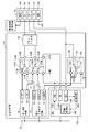
- FIG. 2 is a block diagram showing an example of the configuration of the input / output circuit together with the USB socket and the CPU.
- the input / output circuit 41 includes a first USB circuit 60, a second USB circuit 63, a first analog circuit 70, a second analog circuit 73, a first USB switch 101, and a second USB switch 101A.
- Capacitor C1 Capacitor C1
- common filter 81 common filter 81
- pull-up resistor R resistor
- the first USB switch and the second USB switch 101A are examples of connector switches.
- the USB socket 43 is a connector that can be connected to either an analog cable that can be connected to an analog device that can input analog signals or a USB cable that can be connected to a digital device that can input / output digital signals. .
- the USB socket 43 is a connector having a pin arrangement of mini USB or micro USB defined by the USB standard.
- a case where the USB socket 43 is a connector having a pin arrangement defined by the mini USB standard will be described as an example.
- the USB socket 43 includes a VBUS terminal 140, a D ⁇ terminal 141, a D + terminal 142, an ID terminal 143, and a GND terminal 144.
- FIG. 3 is a diagram illustrating an example of an analog cable.
- the analog cable 1 has a USB plug 45 at one end and two pin plugs 46 and 47 at the other end.
- the USB plug 45 of the analog cable 1 includes a VBUS terminal, a D ⁇ terminal, a D + terminal, an ID terminal, and a GND terminal arranged in accordance with a mini USB pin layout defined by the USB standard.
- the VBUS terminal, D-terminal, ID terminal, and GND terminal of the USB plug 45 are the VBUS terminal 140 of the USB socket 43 of the digital video camera 10.
- D ⁇ terminal 141, D + terminal 142, ID terminal 143, and GND terminal 144 respectively.
- the USB plug 45 electrically connects the ID terminal and the GND terminal.
- the D-terminal of the USB plug 45 is connected to the pin plug 46 via a cable, and the D + terminal of the USB plug 45 is connected to the pin plug 47 via a cable.
- the pin plugs 46 and 47 are connectors that can be respectively connected to analog video input terminals and audio input terminals provided in a display device such as a television receiver or a monitor.
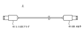
- FIG. 4 is a diagram illustrating an example of a USB cable.
- the USB cable 2 has a USB plug 48 at one end and a USB plug 49 at the other end.
- the USB plug 48 includes a VBUS terminal, a D ⁇ terminal, a D + terminal, and an ID terminal arranged in accordance with the mini USB pin arrangement defined by the USB standard.
- the USB plug 49 is a USB A terminal defined by the USB standard, and includes a VBUS terminal, a D ⁇ terminal, and a D + terminal, and does not have an ID terminal.
- the VBUS terminal, the D ⁇ terminal, and the D + terminal included in the USB plug 48 of the USB cable 2 are electrically connected to the VBUS terminal, the D ⁇ terminal, and the D + terminal included in the USB plug 49 of the USB cable 2 through the cable. Note that the ID terminal of the USB plug 48 of the USB cable 2 is open.
- the USB plug 48 can be connected to a USB socket 43 provided in the digital video camera 10. Therefore, when the USB plug 48 of the USB cable 2 is connected to the USB socket 43 of the digital video camera 10, the VBUS terminal, D ⁇ terminal, D + terminal and ID terminal of the USB plug 48 of the USB cable 2 are connected to the digital video camera.
- the 10 USB sockets 43 are electrically connected to the VBUS terminal 140, the D ⁇ terminal 141, the D + terminal 142, and the ID terminal 143, respectively.
- USB plug 48 of the USB cable 2 When the USB plug 48 of the USB cable 2 is connected to the USB socket 43 of the digital video camera 10, the USB plug 49 is connected to a USB socket provided in an electronic device such as a personal computer (PC).
- PC personal computer
- the CPU 11 is connected to the first USB circuit 60, the second USB circuit 63, the first analog circuit 70, and the second analog circuit 73 via the BUS 39, and the first USB circuit 60 and the second USB circuit 63.
- the first analog circuit 70 and the second analog circuit 73 are controlled.
- the CPU 11 also has a USB-SEL terminal 51, an OE-USB terminal 52, an AV-DET terminal 53, an AV-SEL terminal 54, and an OE-AV terminal 55.
- the first USB circuit 60 is a circuit that is connected to the CPU 11 via the BUS 39 and is controlled by the CPU 11 to input and output USB signals.
- the first USB circuit 60 includes a D-terminal 61 and a D + terminal 62 as digital signal input / output terminals.
- the second USB circuit 63 is connected to the CPU 11 via the BUS 39 and is controlled by the CPU 11 to input / output USB signals.
- the second USB circuit 63 includes a D ⁇ terminal 64 and a D + terminal 65 as digital signal input / output terminals.
- the first USB switch 101 and the second USB switch 101A are electronic components having the same performance with a dynamic range limited to a predetermined range on the plus side.
- the configuration of the first USB switch 101 and the second USB switch 101A is the same.
- the parts included in the first USB switch 101 and the second USB switch 101 ⁇ / b> A are denoted by reference numerals including the same numbers, and the reference numerals appended to the parts included in the second USB switch 101 ⁇ / b> A are assigned to the parts included in the first USB switch 101. This is indicated by a symbol with the letter “A” appended to the number of the appended symbol.
- the first USB switch 101 includes a first switch 110 including terminals 113, 115, and 117, a second switch 120 including terminals 123, 125, and 127, a selection signal input terminal 129, and a connection signal input terminal 131.
- the selection signal input terminal 129 receives a selection signal indicating either the first selection state or the second selection state from the CPU 11 described later.
- the connection signal input terminal 131 receives a connection signal indicating either a connected state or a non-connected state from the CPU 11 described later.
- the first switch 110 is a switch that electrically connects the terminal 115 to one of the terminal 113 and the terminal 117 based on the selection signal input to the selection signal input terminal 129. Specifically, when the selection signal indicating the first selection state is input to the selection signal input terminal 129, the first switch 110 electrically connects the terminal 115 to the terminal 113 and connects the selection signal input terminal 129 to the first signal 110. When a selection signal indicating the two selection state is input, the terminal 115 is electrically connected to the terminal 117.
- the second switch 120 is a switch that electrically connects the terminal 125 to one of the terminal 123 and the terminal 127 based on the selection signal input to the selection signal input terminal 129. Specifically, when the selection signal indicating the first selection state is input to the selection signal input terminal 129, the second switch 120 electrically connects the terminal 125 to the terminal 123 and connects the selection signal input terminal 129 to the first signal. When a selection signal indicating the two selection state is input, the terminal 125 is electrically connected to the terminal 127.
- the first USB switch 101 When the connection signal indicating the connection state is input to the connection signal input terminal 131, the first USB switch 101 activates the first USB switch 101 and the connection signal indicating the non-connection state is input to the connection signal input terminal 131.
- the first USB switch 101 is deactivated. Specifically, when a connection signal indicating a non-connection state is input to the connection signal input terminal 131, the first USB switch 101 opens the circuit by opening the terminals 115 and 125, and connects to the connection signal input terminal 131. When a connection signal indicating a state is input, the circuit is closed without opening the terminals 115 and 125.
- the terminal 113 and the terminal 123 of the first USB switch 101 are connected to the D ⁇ terminal 61 and the D + terminal 62 of the first USB circuit 60, respectively.
- the terminals 117 and 127 of the first USB switch 101 are connected to the D ⁇ terminal 64 and the D + terminal 65 of the second USB circuit 63, respectively.
- the selection signal input terminal 129 and the connection signal input terminal 131 of the first USB switch 101 are connected to the USB-SEL terminal 51 and the OE-USB terminal 52 of the CPU 11, respectively.
- the terminal 115 and the terminal 125 of the first USB switch 101 are connected to the D ⁇ terminal 141 and the D + terminal 142 of the USB socket 43, respectively.
- the first analog circuit 70 is connected to the CPU 11 via the BUS 39 and is controlled by the CPU 11 to output an analog signal.
- the first analog circuit 70 is a circuit that outputs a video signal and an audio signal.
- the first analog circuit 70 includes a VIDEO terminal 72 as an output terminal of a video signal and an AUDIO terminal 71 as an output terminal of an audio signal.
- the audio signal output from the first analog circuit 70 is an analog signal obtained by adding a DC component to an AC audio signal.
- the second analog circuit 73 is a circuit that is connected to the CPU 11 via the BUS 39 and is controlled by the CPU 11 to output an analog signal.
- the second analog circuit 73 is a circuit that outputs a video signal and an audio signal.
- the second analog circuit 73 includes a VIDEO terminal 75 as an output terminal of a video signal and an AUDIO terminal 74 as an output terminal of an audio signal.
- the audio signal output from the second analog circuit 73 is an analog signal obtained by adding a DC component to an AC audio signal.
- the terminals 113A and 123A of the second USB switch 101A are connected to the AUDIO terminal 71 and the VIDEO terminal 72 of the first analog circuit 70, respectively.
- the terminals 117A and 127A of the second USB switch 101A are connected to the AUDIO terminal 74 and the VIDEO terminal 75 of the second analog circuit 73, respectively.
- the selection signal input terminal 129A and the connection signal input terminal 131A of the second USB switch 101A are connected to the AV-SEL terminal 54 and the OE-AV terminal 55 of the CPU 11, respectively.
- the terminal 115A of the second USB switch 101A is connected to one end of the capacitor C1, and the other end of the capacitor C1 is a point in the middle of the connection line connecting the terminal 115 of the first USB switch 101 and the D-terminal 141 of the USB socket 43. Connected to P1.
- the terminal 115A of the second USB switch 101A is connected to the D-terminal 141 of the USB socket 43 via the capacitor C1.
- Capacitor C1 is connected in series between terminal 115A and D-terminal 141.
- the terminal 125A of the second USB switch 101A is connected to a point P2 in the middle of the connection line connecting the terminal 125 of the first USB switch 101 and the D + terminal 142 of the USB socket 43.
- the terminal 125A of the second USB switch 101A is connected to the D + terminal 142 of the USB socket 43.
- the pull-up resistor R connects the ID terminal 143 of the USB socket 43 and the power supply Vdd, and pulls up the voltage of the ID terminal 143.
- the voltage at the ID terminal 143 in a state pulled up by the pull-up resistor R is referred to as a pull-up voltage.
- the common filter 81 is disposed between the terminal 115 of the first USB switch 101 and the D-terminal 141 of the USB socket 43, and between the terminal 125 of the first USB switch 101 and the D + terminal 142 of the USB socket 43.
- the common filter 81 is disposed between the point P1 and the D-terminal 141 and between the point P2 and the D + terminal 142, the terminal 115 of the first USB switch 101 and the D-terminal 141 of the USB socket 43 are disposed.
- the terminal 115 and the point P1 and between the terminal 125 and the point P2 as long as it is between the terminal 125 of the first USB switch 101 and the D + terminal 142 of the USB socket 43.
- the CPU 11 includes a detection unit 56, an operation reception unit 57 that receives a user operation, and a switching control unit 58.
- the detection unit 56 detects the voltage of the AV-DET terminal 53 connected to the ID terminal 143 of the USB socket 43.
- the USB plug 45 of the analog cable 1 is connected to the USB socket 43, since the ID terminal 143 of the USB socket 43 is grounded, the voltage of the AV-DET terminal 53 is lower than the pull-up voltage.
- the USB plug 48 of the USB cable 2 is connected to the USB socket 43, since the ID terminal 143 of the USB socket 43 is opened, the voltage of the AV-DET terminal 53 becomes a pull-up voltage.
- the ID terminal 143 of the USB socket 43 remains open, and the voltage of the AV-DET terminal 53 becomes the pull-up voltage.
- the detection unit 56 detects that the analog cable 1 is connected if the voltage of the AV-DET terminal 53 is smaller than the pull-up voltage.
- the detection unit 56 outputs an analog selection signal to the switching control unit 58 while the voltage at the AV-DET terminal 53 is smaller than the pull-up voltage, but the switching control is performed while the voltage at the AV-DET terminal 53 is during the pull-up voltage.
- a USB selection signal is output to the unit 58.
- the switching control unit 58 switches the connection state of the first USB switch 101 and the second USB switch 101A based on the analog selection signal or the USB selection signal input from the detection unit 56. Specifically, while the USB selection signal is input from the detection unit 56, the switching control unit 58 outputs a connection signal indicating the connection state to the first USB switch 101 and is not connected to the second USB switch 101A. A connection signal indicating is output. In addition, while the analog selection signal is input from the detection unit 56, the switching control unit 58 outputs a connection signal indicating a non-connection state to the first USB switch 101 and a connection indicating a connection state to the second USB switch 101A. Output a signal.
- connection signal indicating the connection state is HI
- connection signal indicating the non-connection state is LO
- the switching control unit 58 sets the OE-USB terminal 52 to HI
- the switching control unit 58 When the switching control unit 58 outputs a connection signal indicating the connection state to the first USB switch 101 and outputs a connection signal indicating the non-connection state to the second USB switch 101A, in other words, the OE-USB terminal 52 is set to HI.
- the OE-AV terminal 55 When the OE-AV terminal 55 is set to LO, the first USB switch 101 is activated and the second USB switch 101A is deactivated. Therefore, any one of the USB socket 43, the first USB circuit 60, and the second USB circuit 63 is connected.
- the switching control unit 58 When the switching control unit 58 outputs a connection signal indicating a disconnected state to the first USB switch 101 and outputs a connection signal indicating a connected state to the second USB switch 101A, in other words, the OE-USB terminal 52 is set to LO.
- the OE-AV terminal 55 When the OE-AV terminal 55 is set to HI, the first USB switch 101 is deactivated and the second USB switch 101A is activated. Accordingly, the USB socket 43 is connected to one of the first analog circuit 70 and the second analog circuit 73.
- the operation reception unit 57 receives an operation input by the user to the operation unit 17.
- the operation unit 17 includes a first setting button and a second setting button.
- the first setting button is a switch for switching between the first USB circuit 60 and the second USB circuit 63.
- the second setting button is a switch for switching between the first analog circuit 70 and the second analog circuit 73.
- the operation accepting unit 57 when the user accepts an operation for switching the second setting button to the first analog circuit setting, the operation accepting unit 57 outputs a selection signal indicating the first selection state to the second USB switch 101A, and the user accepts the second setting button.
- a selection signal indicating the second selection state is output to the second USB switch 101A.
- the selection signal indicating the first selection state is HI
- the selection signal indicating the second selection state is LO.
- the operation accepting unit 57 sets the USB-SEL terminal 51 to HI and accepts an operation for the user to switch the first setting button to the second USB circuit setting.
- the USB-SEL terminal 51 is set to LO.
- the operation accepting unit 57 sets the AV-SEL terminal 54 to HI, and the user performs an operation for switching the second setting button to the second analog circuit setting.
- the AV-SEL terminal 54 is set to LO.
- the operation receiving unit 57 When the operation receiving unit 57 outputs a selection signal indicating the first selection state to the first USB switch 101, in other words, when the USB-SEL terminal 51 is set to HI, the first USB switch 101 is connected to the selection signal input terminal 129. A selection signal indicating the first selection state is input, and the first USB circuit 60 and the USB socket 43 are connected. Specifically, in the first USB switch 101, the first switch 110 connects the terminal 115 to the terminal 113, and the second switch 120 connects the terminal 125 to the terminal 123. When the operation reception unit 57 outputs a selection signal indicating the second selection state to the first USB switch 101, in other words, when the USB-SEL terminal 51 is set to LO, the first USB switch 101 is connected to the selection signal input terminal 129.
- a selection signal indicating the second selection state is input from the CPU 11, and the second USB circuit 63 and the USB socket 43 are connected. Specifically, in the first USB switch 101, the first switch 110 connects the terminal 115 to the terminal 117, and the second switch 120 connects the terminal 125 to the terminal 127.
- the operation reception unit 57 When the operation reception unit 57 outputs a selection signal indicating the first selection state to the second USB switch 101A, in other words, when the AV-SEL terminal 54 is set to HI, the second USB switch 101A is connected to the selection signal input terminal 129A. A selection signal indicating the first selection state is input, and the first analog circuit 70 and the USB socket 43 are connected. Specifically, in the second USB switch 101A, the first switch 110A connects the terminal 115A to the terminal 113A, and the second switch 120A connects the terminal 125A to the terminal 123A.
- the operation reception unit 57 When the operation reception unit 57 outputs a selection signal indicating the second selection state to the second USB switch 101, in other words, when the AV-SEL terminal 54 is set to LO, the selection signal input terminal 129A indicates the second selection state.
- the selection signal is input, and the second USB switch 101 A connects the second analog circuit 73 and the USB socket 43.
- the first switch 110A connects the terminal 115A to the terminal 117A
- the second switch 120A connects the terminal 125A to the terminal 127A.
- the capacitor C1 is connected in series between the terminal 115A of the second USB switch 101A and the D-terminal 141 of the USB socket 43. Since the audio signal output from the first analog circuit 70 or the second analog circuit 73 has a direct current component added thereto, when the first analog circuit 70 or the second analog circuit 73 outputs an audio signal, the USB socket 43 An audio signal from which the DC component has been removed by the capacitor C1 is input to the D-terminal 141.
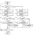
- FIG. 5 is a flowchart showing an example of the flow of the switching process in the first embodiment.
- the switching process is a process executed by the CPU 11 when the CPU 11 executes a switching program stored in the ROM 13.
- CPU 11 determines whether or not the voltage at AV-DET terminal 53 is a pull-up voltage (step S01). If AV-DET terminal 53 is a pull-up voltage (YES in step S01), the process proceeds to step S07. If not (NO in step S01), the process proceeds to step S02.
- step S02 the first USB switch 101 is disconnected and the process proceeds to step S03. Specifically, the CPU 11 outputs a connection signal indicating a non-connected state to the first USB switch 101. In other words, the CPU 11 sets the OE-USB terminal 52 to LO. As a result, the first USB switch 101 opens the terminal 115 and the terminal 125 to open the circuit, resulting in a disconnected state.
- step S03 the second USB switch 101A is set in the connected state, and the process proceeds to step S04. Specifically, the CPU 11 outputs a signal indicating the connection state to the second USB switch 101A. In other words, the CPU 11 sets the OE-AV terminal 55 to HI. As a result, the second USB switch 101A closes the circuit without opening the terminals 115A and 125A, and enters the connected state.
- step S04 it is determined whether the first analog circuit setting is accepted. If the first analog circuit setting is accepted (YES in step S04), the process proceeds to step S05. If not (NO in step S04), the process proceeds to step S06.
- step S05 the first analog circuit 70 is connected, and the process proceeds to step S12. Specifically, the CPU 11 outputs a selection signal indicating the first selection state to the second USB switch 101A. In other words, the CPU 11 sets the AV-SEL terminal 54 to HI. Thus, the second USB switch 101A connects the first analog circuit 70 and the USB socket 43.
- step S06 the second analog circuit 73 is connected, and the process proceeds to step S12. Specifically, the CPU 11 outputs a selection signal indicating the second selection state to the second USB switch 101A. In other words, the CPU 11 sets the AV-SEL terminal 54 to LO. Accordingly, the second USB switch 101A connects the second analog circuit 73 and the USB socket 43.
- step S07 the first USB switch 101 is set in the connected state, and the process proceeds to step S08. Specifically, the CPU 11 outputs a connection signal indicating a connection state to the first USB switch 101. In other words, the CPU 11 sets the OE-USB terminal 52 to HI. As a result, the first USB switch 101 closes the circuit and enters a connected state.
- step S08 the second USB switch 101A is disconnected, and the process proceeds to step S09. Specifically, the CPU 11 outputs a signal indicating a disconnected state to the second USB switch 101A. In other words, the CPU 11 sets the OE-AV terminal 55 to LO. As a result, the second USB switch 101A opens the terminal 115A and the terminal 125A, and enters a disconnected state.
- step S09 it is determined whether the first USB circuit setting is accepted. If the first USB circuit setting is accepted (YES in step S09), the process proceeds to step S10. If not (NO in step S09), the process proceeds to step S11.
- step S10 the first USB circuit 60 is connected, and the process proceeds to step S12. Specifically, the CPU 11 outputs a selection signal indicating the first selection state to the first USB switch 101. In other words, the CPU 11 sets the USB-SEL terminal 51 to HI. Thereby, the first USB switch 101 connects the first USB circuit 60 and the USB socket 43.
- step S11 the second USB circuit 63 is connected, and the process proceeds to step S12. Specifically, the CPU 11 outputs a selection signal indicating the second selection state to the first USB switch 101. In other words, the CPU 11 sets the USB-SEL terminal 51 to LO. Accordingly, the first USB switch 101 connects the second USB circuit 63 and the USB socket 43.
- step S12 it is determined whether or not the power is turned off. If the power is turned off (YES in step S12), the switching process ends. If not (NO in step S12), the process returns to step S01.
- the USB signals input / output by the first USB circuit 60 and the second USB circuit 63 are high-frequency differential digital signals.
- the connection line between the terminal 115 of the first USB switch 101 and the D ⁇ terminal 141 of the USB socket 43 is connected to the capacitor C1 at the point P1, and the terminal 123 of the first USB switch 101 and the D + of the USB socket 43 are connected.
- a connection line to the terminal 142 is connected to the second USB switch 101A at a point P2.
- the first connection line connecting the point P1 and the capacitor C1 and the second connection line connecting the point P2 and the second USB switch 101A are the D ⁇ of the terminal 115 of the first USB switch 101 and the USB socket 43.
- the first USB switch 101 is disposed on the front surface of the double-sided board 20 and the second USB switch is disposed on the rear surface in order to minimize the adverse effects of the first connection line and the second connection line. 101A is arranged.
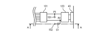
- FIG. 6A is a plan view showing an example of the arrangement of the first USB switch and the second USB switch.
- 6B is a cross-sectional view taken along line AA in FIG. 6A.
- USB socket 43, common filter 81, first USB switch 101, and capacitor C1 are arranged on the front surface of double-sided board 20, and second USB switch 101A is arranged on the back surface.
- the two wiring patterns extending from the common filter 81 are branched at points P1 and P2.
- One wiring pattern branched from the point P1 is connected to the first USB switch 101, and the other wiring patterns are connected to the through hole 151.
- One wiring pattern branched from the point P2 is connected to the first USB switch 101, and the other wiring pattern is connected to the through hole 152 via the capacitor C1.
- a pattern extending from the through hole 151 is connected to the second USB switch 101A, and a pattern extending from the through hole 152 is connected to the second USB switch 101A.
- connection lines for connecting the wiring patterns on the front surface and the wiring patterns on the back surface are arranged.
- the wiring pattern formed between the point P2 and the second USB switch 101A than when arranged on the same surface.
- the length of the wiring pattern formed between the point P2 and the capacitor C1 can be shortened, and adverse effects on the waveform quality can be reduced.
- the digital video camera 10 includes the USB socket 43, the first analog circuit 70 and the second analog circuit 73, the first USB circuit 60 and the second USB circuit 63, and the USB socket. Switching means for connecting 43 to any one of the first analog circuit 70, the second analog circuit 73, the first USB circuit 60, and the second USB circuit 63.
- the USB socket 43 when the analog cable 1 is connected to the USB socket 43, the USB socket 43 is connected to one of the first analog circuit 70 and the second analog circuit 73, and the analog cable 1 is connected to the USB socket 43.
- the USB cable 2 is not connected, particularly when the USB cable 2 is connected to the USB socket 43, the USB socket 43 is connected to one of the first USB circuit 60 and the second USB circuit 63. 43 can output either one of an analog signal and a digital signal. Therefore, it is not necessary to separately provide a connector for outputting an analog signal and a connector for outputting a digital signal, and the number of connectors can be reduced.
- the analog cable 1 connects the ID terminal and the GND terminal, and the USB cable 2 opens the ID terminal, and the ID terminal of the USB socket 43 is pulled up by the pull-up resistor R.
- the ID terminal is grounded, and when the USB cable 2 is connected to the USB socket 43, the ID terminal becomes a pull-up voltage. For this reason, it can be detected that the analog cable 1 is connected to the USB socket 43.
- the capacitor C1 is connected in series between the terminal 115A of the second USB switch 101A and the D-terminal 141 of the USB socket 43, the direct current of the analog signal output from the first analog circuit 70 or the second analog circuit 73 is obtained. An analog signal from which components are removed can be output from the USB socket 43. Further, since the capacitor C1 is connected between the second USB switch 101A and the USB socket 43, an analog signal before removing the DC component is input to the second USB switch 101A. For this reason, the second USB switch 101A whose dynamic range is limited to a predetermined range on the plus side can be used.
- the CPU 11 detects whether the analog cable 1 is connected to the USB socket 43 by detecting the voltage of the ID terminal 143 of the USB socket 43.
- the ID terminal 143 of the USB socket 43 is connected to the connection signal input terminal 131 of the first USB switch 101, and the ID terminal 143 of the USB socket 43 is connected to the second USB via an inverter. Connected to the connection signal input terminal 131A of the switch 101A. In this case, the CPU 11 does not need to include the detection unit 56 and the switching control unit 58.
- the pull-up voltage (HI) is applied to the connection signal input terminal 131 of the first USB switch 101, and the second USB If a voltage (LO) lower than the pull-up voltage is applied to the connection signal input terminal 131A of the switch 101A and the ID terminal 143 of the USB socket 43 is a voltage (LO) lower than the pull-up voltage, the connection signal of the first USB switch 101 A voltage (LO) lower than the pull-up voltage is applied to the input terminal 131, and a pull-up voltage (HI) is applied to the connection signal input terminal 131A of the second USB switch 101A. Also in the digital video camera 10 in the modified example, the same effect as the digital video camera 10 in the first embodiment can be obtained.
- the input / output circuit 41 in the first embodiment uses the first USB switch 101 and the second USB switch 101A whose dynamic range is limited to a predetermined range on the plus side.
- the input / output circuit 41A in the second embodiment is provided with a third USB switch 101B having a predetermined range on the minus side in addition to the plus side instead of the first USB switch 101 and the second USB switch 101A.
- FIG. 7 is a block diagram showing an example of the configuration of the input / output circuit in the second embodiment together with the USB socket and the CPU.
- input / output circuit 41A includes a first USB circuit 60, a first analog circuit 70, a third USB switch 101B, a common filter 81, a pull-up resistor R, and a capacitor C1.
- the third USB switch 101B is an example of a connector switch.
- the CPU 11A is connected to the first analog circuit 70 and the first USB circuit 60 via the BUS 39, and controls the first analog circuit 70 and the first USB circuit 60.
- the CPU 11A includes a SEL terminal 51A, an OE terminal 52A, and a DET terminal 53A.
- the third USB switch 101B is different from the first USB switch 101 and the second USB switch 101A that are limited to a predetermined range on the plus side in that the dynamic range has plus and minus, but the other configuration is the first USB switch 101 and This is the same as the second USB switch 101A.
- the components included in the third USB switch 101 ⁇ / b> B are denoted by reference numerals including the same numbers as the components included in the first USB switch 101, and the reference numerals applied to the components included in the third USB switch 101 ⁇ / b> B are This is indicated by a reference numeral with a letter “B” after the reference numeral assigned to the component.
- the terminals 113B and 123B of the third USB switch 101B are connected to the D ⁇ terminal 61 and the D + terminal 62 of the first USB circuit 60, respectively.
- the terminal 117B of the third USB switch 101B is connected to one end of the capacitor C1, and the other end of the capacitor C1 is connected to the AUDIO terminal 71 of the first analog circuit 70.
- the terminal 127B of the third USB switch 101B is connected to the VIDEO terminal 72 of the first analog circuit 70.
- the selection signal input terminal 129B and the connection signal input terminal 131B of the third USB switch 101B are connected to the SEL terminal 51A and the OE terminal 52A of the CPU 11, respectively.
- the terminal 115B of the third USB switch 101B is connected to the D-terminal 141 of the USB socket 43 via the common filter 81.
- the terminal 125B of the third USB switch 101B is connected to the D + terminal 142 of the USB socket 43 via the common filter 81.
- the capacitor C1 is connected in series between the AUDIO terminal 71 of the first analog circuit 70 and the terminal 117B of the third USB switch 101B. Since the audio signal output from the first analog circuit 70 has a DC component added thereto, when the first analog circuit 70 outputs an audio signal, the DC component is removed from the terminal 117B of the third USB switch 101B by the capacitor C1. Audio signal is input. Since the third USB switch 101B has a predetermined dynamic range of plus and minus, when the first analog circuit 70 outputs an audio signal, the audio signal from which the DC component has been removed by the capacitor C1 is the D of the USB socket 43. -Input to terminal 141.
- the pull-up resistor R connects the ID terminal 143 of the USB socket 43 and the power supply Vdd, and pulls up the voltage of the ID terminal 143.
- the CPU 11 includes a detection unit 56A and a switching control unit 58A.
- the detection unit 56A detects the voltage of the DET terminal 53A.
- the DET terminal 53A is connected to the ID terminal 143 of the USB socket 43.
- the voltage of the DET terminal 53A is lower than the pull-up voltage.
- the USB plug 48 of the USB cable 2 is connected to the USB socket 43, the voltage of the DET terminal 53A becomes a pull-up voltage.
- the voltage of the DET terminal 53A becomes a pull-up voltage.
- the detecting unit 56A detects that the analog cable 1 is connected if the voltage at the DET terminal 53A is smaller than the pull-up voltage.
- the detection unit 56A outputs an analog selection signal to the switching control unit 58A while the voltage at the DET terminal 53A is smaller than the predetermined pull-up voltage, but the switching control unit 58A while the voltage at the DET terminal 53A is the pull-up voltage.
- a USB selection signal is output.
- the switching control unit 58A outputs a connection instruction to the third USB switch 101B based on the analog selection signal or the USB selection signal input from the detection unit 56A. Specifically, the switching control unit 58A outputs a selection signal indicating the first selection state while the USB selection signal is input from the detection unit 56A, and while the analog selection signal is input from the detection unit 56A. The selection signal indicating the second selection state is output. Here, since the selection signal indicating the first selection state is HI and the selection signal indicating the second selection state is LO, the switching control unit 58A selects SEL while the USB selection signal is input from the detection unit 56A. The terminal 51A is set to HI, and the SEL terminal 51A is set to LO while the analog selection signal is input from the detection unit 56A.
- the switching control unit 58A When the switching control unit 58A outputs a selection signal indicating the first selection state to the third USB switch 101B, in other words, when the SEL terminal 51A is set to HI, the third USB switch 101B receives the first signal at the selection signal input terminal 129. A selection signal indicating a selection state is input, and the first USB circuit 60 and the USB socket 43 are connected.
- the switching control unit 58A outputs a selection signal indicating the second selection state to the third USB switch 101B, in other words, when the SEL terminal 51A is set to LO, the third USB switch 101B receives the second signal from the selection signal input terminal 129.
- a selection signal indicating a selection state is input, and the first analog circuit 70 and the USB socket 43 are connected.
- the CPU 11A outputs a connection signal to the third USB switch 101B in order to switch the connection state of the third USB switch 101B.
- a connection signal indicating a connection state may be output to the third USB switch 101B.
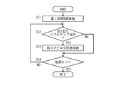
- FIG. 8 is a flowchart showing an example of the flow of switching processing in the second embodiment.
- the switching process is a process executed by the CPU 11A when the CPU 11A executes a switching program stored in the ROM 13.
- CPU 11A determines whether or not the voltage at DET terminal 53A is a pull-up voltage (step S20). If DET terminal 53A is a pull-up voltage (YES in step S20), the process proceeds to step S21. If not (NO in step S20), the process proceeds to step S22.
- step S21 the first USB circuit 60 and the USB socket 43 are connected, and the process proceeds to step S23.
- the CPU 11A outputs a selection signal indicating the first selection state to the third USB switch 101B.
- the CPU 11A sets the SEL terminal 51A to HI.
- the third USB switch 101B connects the first USB circuit 60 and the USB socket 43.
- step S21 the first analog circuit 70 and the USB socket 43 are connected, and the process proceeds to step S23.
- the CPU 11A outputs a selection signal indicating the second selection state to the third USB switch 101B.
- the CPU 11A sets the SEL terminal 51A to LO.
- the third USB switch 101B connects the first analog circuit 70 and the USB socket 43.
- step S23 it is determined whether or not the power is turned off. If the power is turned off (YES in step S23), the switching process ends. If not (NO in step S23), the process returns to step S20.
- the digital video camera 10 when the analog cable 1 is connected to the USB socket 43, the first analog circuit 70 is connected to the USB socket 43, and the analog cable 1 is connected to the USB socket 43. If the USB cable 2 is not connected to the USB socket 43, the USB socket 43 is connected to the first USB circuit 60. For this reason, since both the analog cable 1 and the USB cable 2 can be connected to the USB socket 43, the first analog circuit 70 and the first USB circuit 60 can share one USB socket 43. As a result, since there is no need to provide two sockets corresponding to the first analog circuit 70 and socket corresponding to the first USB circuit 60, the digital video camera 10 can be reduced in size.
- the first analog circuit 70 included in the input / output circuit 41A in the second embodiment is a circuit that outputs a video signal and a monaural audio signal.
- the input / output circuit 41B in the third embodiment includes a third analog circuit 75 that outputs a video signal and a stereo audio signal instead of the first analog circuit 70.
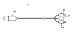
- FIG. 9 is a diagram illustrating an example of an analog cable according to the third embodiment.
- the analog cable 3 has a USB plug 45A at one end and three pin plugs 46, 47, 47A at the other end.
- the USB plug 45A of the analog cable 3 includes a VBUS terminal, a D ⁇ terminal, a D + terminal, an ID terminal, and a GND terminal arranged in accordance with a mini USB pin arrangement defined by the USB standard.
- the VBUS terminal, D-terminal, ID terminal and GND terminal of the USB plug 45A are the VBUS terminal 140 of the USB socket 43 of the digital video camera 10.
- D ⁇ terminal 141, D + terminal 142, ID terminal 143, and GND terminal 144 respectively.
- the D-terminal of the USB plug 45A is connected to the pin plug 46 via a cable
- the D + terminal of the USB plug 45A is connected to the pin plug 47 via a cable
- the ID terminal of the USB plug 45A is connected to the pin plug 47A via a cable.
- the pin plugs 46 and 47 are connectors that can be respectively connected to the right input terminal and the left audio input terminal for inputting analog stereo sound included in a display device such as a television receiver or a monitor.
- the pin plug 47A is a display. It is a connector that can be connected to an analog video input terminal provided in the apparatus. According to the standard, a video input terminal included in a display device is grounded through a 75 ⁇ resistor in the display device.
- FIG. 10 is a block diagram showing an example of the configuration of the input / output circuit in the third embodiment together with the USB socket and the CPU.
- input / output circuit 41B includes a first USB circuit 60, a third analog circuit 75, a third USB switch 101B, a common filter 81, a pull-up resistor R, a video changeover switch 150, a capacitor. C1 and C2.
- the third USB switch 101B is an example of a connector switch.
- the CPU 11B is connected to the third analog circuit 75 and the first USB circuit 60 via the BUS 39, and controls the third analog circuit 75 and the first USB circuit 60.
- the CPU 11B has a SEL terminal 51B, an OE terminal 52B, and a DET terminal 53B. Since the first USB circuit 60 and the third USB switch 101B have been described in the second embodiment, description thereof will not be repeated here.
- the third analog circuit 75 is connected to the CPU 11 via the BUS 39 and is controlled by the CPU 11 to output an analog signal.
- the third analog circuit 75 is a circuit that outputs a video signal, a stereo right audio signal, and a left audio signal.
- the third analog circuit 75 includes a VIDEO terminal 78 as a video signal output terminal, an AUDIO_R terminal 76 as a right audio signal output terminal, and an AUDIO_L terminal 77 as a left audio signal output terminal.
- the right and left audio signals output from the third analog circuit 75 are analog signals obtained by adding a DC component to an AC audio signal.
- the terminals 113B and 123B of the third USB switch 101B are connected to the D ⁇ terminal 61 and the D + terminal 62 of the first USB circuit 60, respectively.
- the terminal 117B of the third USB switch 101B is connected to one end of the capacitor C1, and the other end of the capacitor C1 is connected to the AUDIO_R terminal 76 of the third analog circuit 75.
- the terminal 127B of the third USB switch 101B is connected to one end of the capacitor C2, and the other end of the capacitor C2 is connected to the AUDIO_L terminal 77 of the third analog circuit 75.
- the selection signal input terminal 129B and the connection signal input terminal 131B of the third USB switch 101B are connected to the SEL terminal 51B and the OE terminal 52B of the CPU 11, respectively.
- the terminal 115B of the third USB switch 101B is connected to the D-terminal 141 of the USB socket 43 via the common filter 81.
- the terminal 125B of the third USB switch 101B is connected to the D + terminal 142 of the USB socket 43 via the common filter 81.
- the capacitor C1 is connected in series between the AUDIO_R terminal 76 of the third analog circuit 75 and the terminal 117B of the third USB switch 101B.
- the capacitor C2 is connected in series between the AUDIO_L terminal 77 of the third analog circuit 75 and the terminal 127B of the third USB switch 101B. Since the DC component is added to the right audio signal and the left audio signal output from the third analog circuit 75, when the third analog circuit 75 outputs an audio signal, the capacitor C1 is connected to the terminal 117B of the third USB switch 101B. Thus, the right audio signal from which the DC component has been removed is input, and the left audio signal from which the DC component has been removed by the capacitor C2 is input to the terminal 127B of the third USB switch 101B.
- the third USB switch 101B Since the third USB switch 101B has a predetermined range of positive and negative dynamic ranges, when the third analog circuit 75 outputs an audio signal, the right audio signal and the left audio from which the DC component is removed by the capacitors C1 and C2 Signals are input to the D-terminal 141 and the D + terminal 142 of the USB socket 43, respectively.
- the video changeover switch 150 includes a third switch 151 and a selection signal input terminal 159.
- the third switch 151 includes terminals 153, 155, and 157.
- the selection signal input terminal 159 of the video changeover switch 150 is connected to the SEL terminal 51B of the CPU, and a selection signal indicating either the first selection state or the second selection state is input from the CPU 11. In the selection signal indicating the first selection state, the SEL terminal 51B is HI, and in the selection signal indicating the second selection state, the SEL terminal 51B is LO.
- the third switch 151 is a switch that electrically connects the terminal 155 to one of the terminal 153 and the terminal 157 based on the selection signal input to the selection signal input terminal 159. Specifically, when the selection signal indicating the first selection state is input to the selection signal input terminal 159, in other words, when the SEL terminal 51B is HI, the third switch 151 is connected to the terminal 155 as the terminal 157. When the selection signal indicating the second selection state is input to the selection signal input terminal 159, in other words, when the SEL terminal 51B is LO, the terminal 155 is electrically connected to the terminal 153. .
- the terminal 153 of the third switch 151 is connected to the VIDEO terminal 78 of the third analog circuit 75, and the terminal 155 is connected to the ID terminal 143 of the USB socket 43 and the DET terminal 53B of the CPU.
- a terminal 157 of the third switch 151 is connected to the pull-up resistor R.
- the pull-up resistor R connects the terminal 157 and the power supply Vdd, and pulls up the voltage of the terminal 157.
- the CPU 11 includes a detection unit 56B and a switching control unit 58B.
- the detection unit 56B detects the voltage of the DET terminal 53B.
- the DET terminal 53B is connected to the ID terminal 143 of the USB socket 43 and the terminal 155 of the video changeover switch 150.
- the switching control unit 58B outputs a selection signal indicating the first selection state to the third USB switch 101B at an initial stage immediately after the digital video camera 10 is turned on.
- the SEL terminal 51B is set to HI.
- the selection signal input terminal 159 of the video switch 151 is selected to indicate the first selection state. Since the signal is input, the third switch 151 electrically connects the terminal 155 to the terminal 157.
- the third switch 151 of the video switch 150 connects the terminal 155 and the terminal 157 and the USB plug 48 of the USB cable 2 is connected to the USB socket 43, or nothing is connected to the USB socket 43. If not, the voltage at the DET terminal 53B becomes the pull-up voltage.
- the third switch 151 of the video changeover switch 150 connects the terminal 155 and the terminal 157, and the USB plug 45A of the analog cable 3 is connected to the USB socket 43, the video input terminal of the display device is By installing through a 75 ⁇ resistor, the voltage at the DET terminal 53B becomes lower than the pull-up voltage.
- the detection unit 56B monitors the voltage of the DET terminal 53B after the digital video camera 10 is turned on, and detects that the analog cable 3 is connected when the voltage of the DET terminal 53B becomes smaller than the pull-up voltage. .
- the detection unit 56B outputs a USB selection signal to the switching control unit 58B after the digital video camera 10 is turned on. However, after detecting that the analog cable 3 is connected, the detection unit 56B outputs an analog signal to the switching control unit 58B. Outputs a selection signal.
- the switching control unit 58B outputs a connection instruction to the third USB switch 101B based on the analog selection signal or the USB selection signal input from the detection unit 56B. Specifically, the switching control unit 58B outputs a selection signal indicating the first selection state while the USB selection signal is input from the detection unit 56B, and while the analog selection signal is input from the detection unit 56B. The selection signal indicating the second selection state is output. Here, since the selection signal indicating the first selection state is set to HI and the selection signal indicating the second selection state is set to LO, the switching control unit 58B selects SEL while the USB selection signal is input from the detection unit 56B. The terminal 51B is set to HI, and the SEL terminal 51B is set to LO while the analog selection signal is input from the detection unit 56B.
- the switching control unit 58B When the switching control unit 58B outputs a selection signal indicating the first selection state to the third USB switch 101B, in other words, when the SEL terminal 51B is set to HI, the third USB switch 101B receives the first signal from the selection signal input terminal 129B. A selection signal indicating a selection state is input, and the first USB circuit 60 and the USB socket 43 are connected.
- the switching control unit 58B When the switching control unit 58B outputs a selection signal indicating the second selection state to the third USB switch 101B, in other words, when the SEL terminal 51B is set to LO, the third USB switch 101B receives the second signal from the selection signal input terminal 129B.
- a selection signal indicating a selection state is input, and the AUDIO_R terminal 76 of the third analog circuit 75 and the D ⁇ terminal 141 of the USB socket 43 are connected, and the AUDIO_L terminal 77 of the third analog circuit 75 and the D + terminal of the USB socket 43 are connected. 142 is connected.
- the CPU 11B outputs a connection signal to the third USB switch 101B in order to switch the connection state of the third USB switch 101B. While either the USB cable 2 or the analog cable 3 is connected to the USB socket 43, A connection signal indicating a connection state may be output to the third USB switch 101B.
- the switching control unit 58B When the switching control unit 58B outputs a selection signal indicating the first selection state to the third USB switch 101B, in other words, when the SEL terminal 51B is set to HI, the video switch 150 is connected to the selection signal input terminal 159. A selection signal indicating the first selection state is input, and the ID terminal 143 of the USB socket 43 and the DET terminal 53B of the CPU 11B are connected to the pull-up power supply Vdd via the pull-up resistor R.
- the switching control unit 58B When the switching control unit 58B outputs a selection signal indicating the second selection state to the third USB switch 101B, in other words, when the SEL terminal 51B is set to LO, the video switch 150 is connected to the selection signal input terminal 159 with the second signal. A selection signal indicating the selection state is input, and the VIDEO terminal 78 of the second analog circuit 75 and the ID terminal 143 of the USB socket 43 are connected.
- FIG. 11 is a flowchart showing an example of the flow of switching processing in the third embodiment.
- the switching process is a process executed by the CPU 11B when the CPU 11B executes a switching program stored in the ROM 13.
- CPU 11 ⁇ / b> B connects first USB circuit 60 and USB socket 43.
- the CPU 11B outputs a selection signal indicating the first selection state to the third USB switch 101B.
- the CPU 11A sets the SEL terminal 51A to HI.
- the third USB switch 101B connects the first USB circuit 60 and the USB socket 43.
- step S32 it is determined whether or not the voltage of the DET terminal 53B is smaller than the pull-up voltage. If DET terminal 53B is smaller than the pull-up voltage (YES in step S32), the process proceeds to step S33; otherwise (NO in step S32), the process proceeds to step S34.
- step S33 the third analog circuit 75 and the USB socket 43 are connected, and the process proceeds to step S34.
- the CPU 11B outputs a selection signal indicating the second selection state to the third USB switch 101B.
- the CPU 11B sets the SEL terminal 51B to LO.
- the third USB switch 101B connects the AUDIO_R terminal 76 of the third analog circuit 75 and the D-terminal 141 of the USB socket 43, and also the AUDIO_L terminal 77 of the third analog circuit 75 and the D + terminal 142 of the USB socket 43.
- the video changeover switch 150 connects the VIDEO terminal 78 of the second analog circuit 75 and the ID terminal 143 of the USB socket 43.
- step S34 it is determined whether or not the power is turned off. If the power is turned off (YES in step S34), the switching process ends. If not (NO in step S34), the process returns to step S32.
- the digital video camera 10 after the power is turned on, when the analog cable 3 is not connected to the USB socket 43, particularly when the USB cable 2 is connected to the USB socket 43, The USB socket 43 is connected to the first USB circuit 60. Then, after the analog cable 3 is connected to the USB socket 43, the third analog circuit 75 is connected to the USB socket 43. For this reason, since both the analog cable 3 and the USB cable 2 can be connected to the USB socket 43, the third analog circuit 75 and the first USB circuit 60 may share one USB socket 43. is there.
Landscapes
- Engineering & Computer Science (AREA)
- Physics & Mathematics (AREA)
- General Engineering & Computer Science (AREA)
- Theoretical Computer Science (AREA)
- Mathematical Physics (AREA)
- Computer Hardware Design (AREA)
- General Physics & Mathematics (AREA)
- Information Transfer Systems (AREA)
Abstract
【課題】 コネクタの数を少なくすること。 【解決手段】 デジタルビデオカメラは、アナログ信号を入力可能なアナログ機器と接続可能なアナログケーブルおよびUSB信号を入出力可能なデジタル機器と接続可能なデジタルケーブルのうちいずれか一方と接続が可能なUSBソケット43と、アナログ信号を出力する第1および第2アナログ回路70,71と、USB信号を入出力する第1および第2USB回路60,63と、USBソケット43を、第1および第2アナログ回路70,71、第1および第2USB回路60,63のいずれかと接続するUSBスイッチ110,110Aと、を備える。
Description
この発明は、電子機器に関し、特に外部にアナログまたはデジタルの2種類の信号を出力可能な電子機器に関する。
外部に接続される機器に応じてデジタル信号とアナログ信号のいずれかを出力する電子機器が知られている。特開2006-293440号公報(特許文献1)には、外部からの制御信号を入力する入力端子、アナログ信号を出力するアナログ出力端子及びデジタル信号を出力するデジタル出力端子を含む機器コネクタを有する機器との接続が可能な電気機器において、前記機器コネクタとの接続が可能な接続コネクタを備え、該接続コネクタは、前記入力端子との接続を行なって制御信号を出力する出力端子と、前記アナログ出力端子から出力されたアナログ信号を入力するアナログ入力端子と、前記デジタル出力端子から出力されたデジタル信号を入力するデジタル入力端子と、を含むことを特徴とする電気機器が記載されている。
しかしながら、従来の電気機器は、アナログ信号用の端子と、デジタル信号用の端子とを設けなければならない。特に、外部の機器と接続される端子を含むコネクタは、機器の外部からケーブルが接続できるように、外装に設けなければならない。このため、機器を小型化することができないといった問題があった。
特開2006-293440号公報
この発明は上述した問題点を解決するためになされたもので、この発明の目的の1つは、コネクタの数を少なくした電子機器を提供することである。
上述した目的を達成するためにこの発明のある局面によれば、電子機器は、アナログ信号を入力可能なアナログ機器と接続可能なアナログケーブルおよびデジタル信号を入出力可能なデジタル機器と接続可能なデジタルケーブルのうちいずれか一方と接続が可能なコネクタと、アナログ信号を出力するアナログ回路と、デジタル信号を入出力するデジタル回路と、コネクタを、アナログ回路およびデジタル回路のいずれか一方と接続する切換手段と、を備える。
例えば、デジタル回路がUSB回路である場合、コネクタを、アナログ回路およびUSB回路のいずれか一方と接続するので、1つのコネクタからアナログ信号とUSB信号とのいずれか一方を出力することができる。その結果、コネクタの数を少なくした電子機器を提供することができる。
好ましくは、コネクタは、ID端子とGND端子とデータ通信端子とを少なくとも有し、アナログケーブルは、ID端子とGND端子とを接続しており、USBケーブルは、ID端子を開放しており、切換手段は、ID端子を所定の電圧にプルアップするプルアップ手段と、ID端子の電圧を検出する検出手段と、を含む。
この局面に従えば、コネクタにアナログケーブルが接続されると、ID端子が接地され、コネクタにUSBケーブルが接続されると、ID端子が所定の電圧にプルアップされる。このため、コネクタにアナログケーブルが接続されたことを検出することができる。
好ましくは、切換手段は、ダイナミックレンジがプラス側の所定範囲に制限され、コネクタとUSB回路との間に設けられ、コネクタのデータ通信端子とUSB回路とを接続する接続状態および非接続状態のいずれかに切り換える第1コネクタスイッチと、ダイナミックレンジがプラス側の所定範囲に制限され、コネクタとアナログ回路との間に設けられ、コネクタのデータ通信端子とアナログ回路とを接続する接続状態および非接続状態のいずれかに切り換える第2コネクタスイッチと、第1コネクタスイッチおよび第2コネクタスイッチを制御する制御手段と、第2コネクタスイッチとコネクタとの間に直列接続されるコンデンサと、を含み、制御手段は、検出手段と、検出手段により所定の電圧が検出される間は、第1コネクタスイッチを接続状態にし、第2コネクタスイッチを非接続状態にし、検出手段により所定の電圧が検出されない間は、第2コネクタスイッチを接続状態にし、第1コネクタスイッチを非接続状態にする切換制御手段と、を含む。
この局面に従えば、アナログ回路とコネクタのとの間にコンデンサが直列に接続されるので、アナログ回路から出力されるアナログ信号の直流成分を除去したアナログ信号をコネクタから出力することができる。また、コンデンサが、第2コネクタスイッチとコネクタとの間に接続されるので、直流成分を除去する前のアナログ信号が第2コネクタスイッチに入力されるので、ダイナミックレンジがプラス側の所定範囲に制限される第2コネクタスイッチを用いることができる。
好ましくは、データ通信端子は、第1のデータ通信端子と、第2のデータ通信端子と、を含み、アナログ回路は、ビデオ信号出力端子と、オーディオ信号出力端子と、を有し、アナログ回路は、ビデオ信号出力端子からビデオ信号出力し、オーディオ信号出力端子からオーディオ信号を出力し、第1のデータ通信端子は、ビデオ信号出力端子と接続され、第2のデータ通信端子は、オーディオ信号出力端子と接続され、コンデンサは、第2のデータ通信端子とオーディオ信号出力端子との間に接続される。
好ましくは、切換手段は、コネクタとアナログ回路およびUSB回路との間に設けられ、コネクタのデータ通信端子をアナログ回路とUSB回路とのいずれか一方に接続するコネクタスイッチと、コネクタスイッチを制御する制御手段と、を含み、制御手段は、検出手段と、検出手段により所定の電圧が検出される間は、コネクタのデータ通信端子をUSB回路に接続する指示をコネクタスイッチに出力し、検出手段により所定の電圧が検出されない間は、コネクタのデータ通信端子をアナログ回路に接続する指示をコネクタスイッチに出力する切換制御手段と、を含む。
この局面に従えば、コネクタにアナログケーブルが接続される場合に、コネクタにアナログ回路を接続し、コネクタにアナログケーブルが接続されていない場合に、コネクタにUSB回路を接続する。このため、コネクタに接続されるケーブルに対応して回路を切り換えることが可能な電子機器を提供することができる。
好ましくは、コネクタは、ID端子とGND端子とデータ通信端子とを少なくとも有し、アナログケーブルに接続されるアナログ機器は、アナログケーブルがコネクタに接続された状態で、ID端子を接地し、デジタルケーブルは、ID端子を開放しており、切換手段は、ID端子を所定の電圧にプルアップするプルアップ手段と、ID端子の電圧を検出する検出手段と、を含む。
好ましくは、切換手段は、検出手段により所定の値よりも小さいID端子の電圧が検出された後は、ID端子をアナログ回路と接続する切換スイッチを含む。
好ましくは、切換手段は、コネクタとアナログ回路およびデジタル回路との間に設けられ、コネクタのデータ通信端子をアナログ回路とデジタル回路とのいずれか一方に接続するコネクタスイッチと、コネクタスイッチを制御する制御手段と、をさらに含み、制御手段は、検出手段と、検出手段により所定の値よりも小さいID端子の電圧が検出される前は、コネクタのデータ通信端子をデジタル回路に接続する指示をコネクタスイッチに出力し、検出手段により所定の値よりも小さいID端子の電圧が検出された後は、コネクタのデータ通信端子をアナログ回路に接続する指示をコネクタスイッチに出力する切換制御手段と、を含む。
以下、本発明の実施の形態について図面を参照して説明する。以下の説明では同一の部品には同一の符号を付してある。それらの名称および機能も同じである。したがってそれらについての詳細な説明は繰り返さない。
<第1の実施の形態>
本実施の形態においては、電子機器の一例としてビデオカメラについて説明する。図1は、本実施の形態の1つにおけるビデオカメラの構成の概略を示すブロック図である。図1を参照して、デジタルビデオカメラ10は、デジタルビデオカメラ10の全体を制御する中央演算装置(CPU)11と、CPU11が実行するためのプログラム等を記憶するROM(Read Only Memory)13と、イメージセンサ15と、操作部17と、マイクロホン21と、アナログ/デジタル変換部(A/D)19,23と、メモリ制御部25と、SDRAM(Synchronous Dynamic Random Access Memory)27と、液晶表示装置(LCD)31と、LCDドライバ29と、JPEG(Joint Photographic Experts Group)-CODEC33と、MPEG(Moving Picture Experts Group)-CODEC35と、大容量記憶装置としてのハードディスクドライブ(HDD)37と、入出力回路41と、USBソケット43と、を含む。
本実施の形態においては、電子機器の一例としてビデオカメラについて説明する。図1は、本実施の形態の1つにおけるビデオカメラの構成の概略を示すブロック図である。図1を参照して、デジタルビデオカメラ10は、デジタルビデオカメラ10の全体を制御する中央演算装置(CPU)11と、CPU11が実行するためのプログラム等を記憶するROM(Read Only Memory)13と、イメージセンサ15と、操作部17と、マイクロホン21と、アナログ/デジタル変換部(A/D)19,23と、メモリ制御部25と、SDRAM(Synchronous Dynamic Random Access Memory)27と、液晶表示装置(LCD)31と、LCDドライバ29と、JPEG(Joint Photographic Experts Group)-CODEC33と、MPEG(Moving Picture Experts Group)-CODEC35と、大容量記憶装置としてのハードディスクドライブ(HDD)37と、入出力回路41と、USBソケット43と、を含む。
CPU11、メモリ制御部25、JPEG‐CODEC33、MPEG‐CODEC35および入出力回路41それぞれは、バス39に接続されている。イメージセンサ15は、レンズを介して結像する被写体像の画像を光電変換した画像をA/D19に出力する。A/D19は、入力されるアナログ信号の画像のデータをデジタル信号に変換し、メモリ制御部25に出力する。
また、マイクロホン21は、音を集音し、アナログ信号の音データを、A/D23に出力する。A/D23は、マイクロホン21から入力されるアナログ信号の音データをデジタル信号に変換し、メモリ制御部25に出力する。
メモリ制御部25は、A/D19から入力される画像をSDRAM27の表示画像エリアに格納し、A/D23から入力される音をSDRAM27の音エリアに格納する。LCDドライバ29は、SDRAM27の表示画像エリアに格納された画像のデジタル信号のデータを、R(赤)G(緑)B(青)のアナログ信号のデータに変換し、LCD31に出力する。これにより、LCD31に画像が表示される。
操作部17は、ユーザの操作を受け付けるための複数のボタンを有する。また、操作部17は、LCD31に重畳して設けられるタッチパネルを含み、ユーザがLCD31の表示面を指で指示すると、指示された位置を受け付ける。
JPEG-CODEC33は、CPU11により制御され、SDRAM27に格納されたデジタル信号の画像データを圧縮符合化し、JPEGフォーマットの符号化データに変換し、また、JPEGフォーマットの符号化データを復号し、デジタル信号の画像データに変換する。
MPEG-CODEC35は、CPU11により制御され、SDRAM27に時系列に格納される複数フレームの画像のデータと、音のデータとを圧縮符号化し、MPEGフォーマットの符号化データに変換し、また、MPEGフォーマットの符号化データを復号し、画像のデータと音のデータとに変換する。JPEG-CODEC33が、1フレームの画像を符号化または復号するのに対して、MPEG-CODEC35は、複数フレームの画像からなる動画像と音のデータを符号化または復号する。
HDD37には、JPEG-CODEC33によりJPEGフォーマットに変換された符号化データおよびMPEG-CODEC35によりMPEGフォーマットに変換された符号化データが記憶される。
なお、ここでは、大容量記憶装置としてHDD37を備える例を説明したが、HDD37に代えて、内蔵のフラッシュメモリであってもよいし、着脱可能な光ディスク(CD-ROM(Compact Disc-Read Only Memory)/MO(Magnetic Optical Disc/MD(Mini Disc)/DVD(Digital Versatile Disc))、ICカード(メモリカードを含む)、光カード、マスクROM、EPROM(Erasable Programmable ROM)、EEPROM(Electrically EPROM)などを用いてもよい。
図2は、入出力回路の構成の一例をUSBソケットおよびCPUとともに示すブロック図である。図2を参照して、入出力回路41は、第1USB回路60と、第2USB回路63と、第1アナログ回路70と、第2アナログ回路73と、第1USBスイッチ101と、第2USBスイッチ101Aと、コンデンサC1と、コモンフィルタ81と、プルアップ抵抗Rと、を含む。第1USBスイッチおよび第2USBスイッチ101Aは、コネクタスイッチの一例である。
USBソケット43は、アナログ信号を入力可能なアナログ機器と接続が可能なアナログケーブルおよびデジタル信号を入出力可能なデジタル機器と接続が可能なUSBケーブルのうちいずれか一方と接続が可能なコネクタである。USBソケット43は、USB規格で定められたミニUSBまたはマイクロUSBのピン配置を有するコネクタである。ここでは、USBソケット43を、ミニUSBの規格で定められたピン配置のコネクタとする場合を例に説明する。USBソケット43は、VBUS端子140と、D-端子141と、D+端子142と、ID端子143と、GND端子144と、を含む。
ここで、USBソケット43に接続可能なUSBケーブルおよびアナログケーブルについて説明する。図3は、アナログケーブルの一例を示す図である。図3を参照して、アナログケーブル1は、一端にUSBプラグ45を有し、他端に2つのピンプラグ46,47を有する。アナログケーブル1のUSBプラグ45は、USB規格で定められたミニUSBのピン配置に従って配置されたVBUS端子、D-端子、D+端子、ID端子およびGND端子を含む。USBプラグ45がデジタルビデオカメラ10のUSBソケット43に接続されると、USBプラグ45が有するVBUS端子、D-端子、ID端子およびGND端子は、デジタルビデオカメラ10のUSBソケット43が有するVBUS端子140、D-端子141、D+端子142、ID端子143およびGND端子144とそれぞれ電気的に接続される。
USBプラグ45は、ID端子とGND端子とを電気的に接続している。USBプラグ45のD-端子はピンプラグ46とケーブルによって接続されており、USBプラグ45のD+端子はピンプラグ47とケーブルによって接続されている。ピンプラグ46,47は、テレビジョン受像機、モニター等の表示装置が備えるアナログの映像入力端子および音声入力端子とそれぞれ接続可能なコネクタである。
図4は、USBケーブルの一例を示す図である。図4を参照して、USBケーブル2は、一端にUSBプラグ48を有し、他端にUSBプラグ49を有する。USBプラグ48は、USB規格で定められたミニUSBのピン配置に従って配置されたVBUS端子、D-端子、D+端子およびID端子を含む。USBプラグ49は、USB規格で定められたUSB A端子であり、VBUS端子、D-端子およびD+端子を含み、ID端子を有さない。USBケーブル2のUSBプラグ48が有するVBUS端子、D-端子、D+端子は、USBケーブル2のUSBプラグ49が有するVBUS端子、D-端子、D+端子とケーブルで電気的にそれぞれ接続される。なお、USBケーブル2のUSBプラグ48が有するID端子は、開放されている。
USBプラグ48は、デジタルビデオカメラ10に設けられたUSBソケット43と接続が可能である。したがって、USBケーブル2のUSBプラグ48がデジタルビデオカメラ10のUSBソケット43に接続されると、USBケーブル2のUSBプラグ48が有するVBUS端子、D-端子、D+端子およびID端子は、デジタルビデオカメラ10のUSBソケット43が有するVBUS端子140、D-端子141、D+端子142およびID端子143とそれぞれ電気的に接続される。
USBケーブル2のUSBプラグ48がデジタルビデオカメラ10が有するUSBソケット43に接続される場合、USBプラグ49は、パーソナルコンピューター(PC)等の電子機器に設けられたUSBソケットと接続される。
図2に戻って、CPU11は、BUS39を介して、第1USB回路60、第2USB回路63、第1アナログ回路70、第2アナログ回路73と接続されており、第1USB回路60、第2USB回路63、第1アナログ回路70および第2アナログ回路73をそれぞれ制御する。また、CPU11は、USB-SEL端子51、OE-USB端子52、AV-DET端子53、AV-SEL端子54およびOE-AV端子55と、を有する。
第1USB回路60は、CPU11とBUS39を介して接続され、CPU11により制御されてUSB信号を入出力する回路である。第1USB回路60は、デジタル信号の入出力端子としてD-端子61と、D+端子62と、を含む。
第2USB回路63は、CPU11とBUS39を介して接続され、CPU11により制御されてUSB信号を入出力する回路である。第2USB回路63は、デジタル信号の入出力端子としてD-端子64と、D+端子65と、を含む。
第1USBスイッチ101と、第2USBスイッチ101Aとは、ダイナミックレンジがプラス側の所定の範囲に制限された同じ性能を有する電子部品である。第1USBスイッチ101および第2USBスイッチ101Aの構成は同じである。図2においては、第1USBスイッチ101および第2USBスイッチ101Aそれぞれが有する部品には同じ数字を含む符号を付し、第2USBスイッチ101Aが有する部品に付した符号は、第1USBスイッチ101が有する部品に付した符号の番号の後に文字「A」を添えた符号で示している。
ここでは、第1USBスイッチ101を例にその構成を説明する。第1USBスイッチ101は、端子113、115、117を含む第1スイッチ110と、端子123、125、127を含む第2スイッチ120と、選択信号入力端子129と、接続信号入力端子131と、を含む。選択信号入力端子129は、後述するCPU11から第1選択状態または第2選択状態のいずれかを示す選択信号が入力される。接続信号入力端子131は、後述するCPU11から接続状態または非接続状態のいずれかを示す接続信号が入力される。
第1スイッチ110は、選択信号入力端子129に入力される選択信号に基づいて、端子115を、端子113および端子117のいずれか一方と電気的に接続するスイッチである。具体的には、第1スイッチ110は、選択信号入力端子129に第1選択状態を示す選択信号が入力される場合は端子115を端子113と電気的に接続し、選択信号入力端子129に第2選択状態を示す選択信号が入力される場合は端子115を端子117と電気的に接続する。
第2スイッチ120は、選択信号入力端子129に入力される選択信号に基づいて、端子125を、端子123および端子127のいずれか一方と電気的に接続するスイッチである。具体的には、第2スイッチ120は、選択信号入力端子129に第1選択状態を示す選択信号が入力される場合は端子125を端子123と電気的に接続し、選択信号入力端子129に第2選択状態を示す選択信号が入力される場合は端子125を端子127と電気的に接続する。
また、第1USBスイッチ101は、接続信号入力端子131に接続状態を示す接続信号が入力される場合、第1USBスイッチ101を能動化し、接続信号入力端子131に非接続状態を示す接続信号が入力される場合、第1USBスイッチ101を非能動化する。具体的には、第1USBスイッチ101は、接続信号入力端子131に非接続状態を示す接続信号が入力される場合、端子115および端子125を開放して回路を開き、接続信号入力端子131に接続状態を示す接続信号が入力される場合、端子115および端子125を開放することなく回路を閉じる。
第1USBスイッチ101の端子113および端子123は、第1USB回路60のD-端子61およびD+端子62にそれぞれ接続される。第1USBスイッチ101の端子117および端子127は、第2USB回路63のD-端子64およびD+端子65にそれぞれ接続される。第1USBスイッチ101の選択信号入力端子129および接続信号入力端子131は、CPU11のUSB-SEL端子51およびOE-USB端子52とそれぞれと接続される。第1USBスイッチ101の端子115および端子125は、USBソケット43のD-端子141およびD+端子142とそれぞれ接続される。
第1アナログ回路70は、CPU11とBUS39を介して接続され、CPU11により制御されてアナログ信号を出力する回路である。ここでは、第1アナログ回路70を、ビデオ信号とオーディオ信号とを出力する回路としている。第1アナログ回路70は、ビデオ信号の出力端子としてVIDEO端子72と、オーディオ信号の出力端子としてAUDIO端子71と、を含む。第1アナログ回路70が出力するオーディオ信号は、交流のオーディオ信号に直流成分が付加されたアナログ信号である。
第2アナログ回路73は、CPU11とBUS39を介して接続され、CPU11により制御されてアナログ信号を出力する回路である。ここでは、第2アナログ回路73を、ビデオ信号とオーディオ信号とを出力する回路としている。第2アナログ回路73は、ビデオ信号の出力端子としてVIDEO端子75と、オーディオ信号の出力端子としてAUDIO端子74と、を含む。第2アナログ回路73が出力するオーディオ信号は、交流のオーディオ信号に直流成分が付加されたアナログ信号である。
第2USBスイッチ101Aの端子113Aおよび端子123Aは、第1アナログ回路70のAUDIO端子71およびVIDEO端子72にそれぞれ接続される。第2USBスイッチ101Aの端子117Aおよび端子127Aは、第2アナログ回路73のAUDIO端子74およびVIDEO端子75にそれぞれ接続される。第2USBスイッチ101Aの選択信号入力端子129Aおよび接続信号入力端子131Aは、CPU11のAV-SEL端子54およびOE-AV端子55にそれぞれ接続される。第2USBスイッチ101Aの端子115Aは、コンデンサC1の一端に接続され、コンデンサC1の他端は、第1USBスイッチ101の端子115とUSBソケット43のD-端子141とを接続する接続線の途中の点P1に接続される。換言すれば、第2USBスイッチ101Aの端子115Aは、USBソケット43のD-端子141と、コンデンサC1を介して接続される。コンデンサC1は、端子115AとD-端子141との間に直列に接続される。
第2USBスイッチ101Aの端子125Aは、第1USBスイッチ101の端子125とUSBソケット43のD+端子142とを接続する接続線の途中の点P2に接続される。換言すれば、第2USBスイッチ101Aの端子125Aは、USBソケット43のD+端子142と接続される。
プルアップ抵抗Rは、USBソケット43のID端子143と電源Vddとを接続し、ID端子143の電圧をプルアップする。以下、プルアップ抵抗Rによりプルアップされた状態におけるID端子143の電圧をプルアップ電圧という。
コモンフィルタ81は、第1USBスイッチ101の端子115とUSBソケット43のD-端子141との間、および第1USBスイッチ101の端子125とUSBソケット43のD+端子142との間に配置される。なお、コモンフィルタ81を、点P1とD-端子141との間および点P2とD+端子142との間に配置しているが、第1USBスイッチ101の端子115とUSBソケット43のD-端子141との間、および第1USBスイッチ101の端子125とUSBソケット43のD+端子142との間であれば、端子115と点P1との間、および端子125と点P2との間であってもよい。
CPU11は、検出部56と、ユーザの操作を受け付ける操作受付部57と、切換制御部58と、を含む。検出部56は、USBソケット43のID端子143と接続されるAV-DET端子53の電圧を検出する。USBソケット43にアナログケーブル1のUSBプラグ45が接続される場合、USBソケット43のID端子143が接地されるので、AV-DET端子53の電圧がプルアップ電圧より低い電圧となる。一方、USBソケット43にUSBケーブル2のUSBプラグ48が接続される場合、USBソケット43のID端子143が開放されるので、AV-DET端子53の電圧がプルアップ電圧となる。USBソケット43に何も接続されていない場合、USBソケット43のID端子143が開放されたままなので、AV-DET端子53の電圧がプルアップ電圧となる。
検出部56は、AV-DET端子53の電圧がプルアップ電圧より小さければ、アナログケーブル1が接続されたことを検出する。検出部56は、AV-DET端子53の電圧がプルアップ電圧より小さい間、切換制御部58に、アナログ選択信号を出力するが、AV-DET端子53の電圧がプルアップ電圧の間、切換制御部58に、USB選択信号を出力する。
切換制御部58は、検出部56から入力されるアナログ選択信号またはUSB選択信号に基づいて、第1USBスイッチ101および第2USBスイッチ101Aの接続状態を切り換える。具体的には、切換制御部58は、検出部56からUSB選択信号が入力されている間は、第1USBスイッチ101に接続状態を示す接続信号を出力するとともに、第2USBスイッチ101Aに非接続状態を示す接続信号を出力する。また、切換制御部58は、検出部56からアナログ選択信号が入力されている間は、第1USBスイッチ101に非接続状態を示す接続信号を出力するとともに、第2USBスイッチ101Aに接続状態を示す接続信号を出力する。ここでは、接続状態を示す接続信号をHI、非接続状態を示す接続信号をLOとしている。切換制御部58は、検出部56からUSB選択信号が入力されている間は、OE-USB端子52をHIにするとともに、OE-AV端子55をLOにし、検出部56からアナログ選択信号が入力されている間は、OE-USB端子52をLOにするとともに、OE-AV端子55をHIにする。
切換制御部58が第1USBスイッチ101に接続状態を示す接続信号を出力するとともに、第2USBスイッチ101Aに非接続状態を示す接続信号を出力する場合、換言すれば、OE-USB端子52をHIにし、OE-AV端子55をLOにする場合、第1USBスイッチ101は能動化し、第2USBスイッチ101Aは非能動化する。したがって、USBソケット43と、第1USB回路60と第2USB回路63のいずれか一方が、接続される。
切換制御部58が第1USBスイッチ101に非接続状態を示す接続信号を出力するとともに、第2USBスイッチ101Aに接続状態を示す接続信号を出力する場合、換言すれば、OE-USB端子52をLOにし、OE-AV端子55をHIにする場合、第1USBスイッチ101は非能動化し、第2USBスイッチ101Aは能動化する。したがって、USBソケット43と、第1アナログ回路70と第2アナログ回路73のいずれか一方が、接続される。
操作受付部57は、ユーザが操作部17に入力する操作を受け付ける。操作部17は、第1設定ボタンと第2設定ボタンとを有する。第1設定ボタンは、第1USB回路60と第2USB回路63とを切り換えるスイッチである。第2設定ボタンは、第1アナログ回路70と第2アナログ回路73とを切り換えるスイッチである。操作受付部57は、ユーザが第1設定ボタンを第1USB回路設定に切り換える操作を受け付けると、第1USBスイッチ101に第1選択状態を示す選択信号を出力し、ユーザが第1設定ボタンを第2USB回路設定に切り換える操作を受け付けると、第1USBスイッチ101に第2選択状態を示す選択信号を出力する。また、操作受付部57は、ユーザが第2設定ボタンを第1アナログ回路設定に切り換える操作を受け付けると、第2USBスイッチ101Aに第1選択状態を示す選択信号を出力し、ユーザが第2設定ボタンを第2アナログ回路設定に切り換える操作を受け付けると、第2USBスイッチ101Aに第2選択状態を示す選択信号を出力する。
ここでは、第1選択状態を示す選択信号をHI、第2選択状態を示す選択信号をLOとしている。操作受付部57は、ユーザが第1設定ボタンを第1USB回路設定に切り換える操作を受け付けると、USB-SEL端子51をHIにし、ユーザが第1設定ボタンを第2USB回路設定に切り換える操作を受け付けると、USB-SEL端子51をLOにする。操作受付部57は、ユーザが第2設定ボタンを第1アナログ回路設定に切り換える操作を受け付けると、AV-SEL端子54をHIにし、ユーザが第2設定ボタンを第2アナログ回路設定に切り換える操作を受け付けると、AV-SEL端子54をLOにする。
操作受付部57が第1USBスイッチ101に第1選択状態を示す選択信号を出力する場合、換言すれば、USB-SEL端子51をHIにする場合、第1USBスイッチ101は、選択信号入力端子129に第1選択状態を示す選択信号が入力され、第1USB回路60とUSBソケット43とを接続する。具体的には、第1USBスイッチ101は、第1スイッチ110が端子115を端子113と接続し、第2スイッチ120が端子125を端子123と接続する。操作受付部57が第1USBスイッチ101に第2選択状態を示す選択信号を出力する場合、換言すれば、USB-SEL端子51をLOにする場合、第1USBスイッチ101は、選択信号入力端子129にCPU11から第2選択状態を示す選択信号が入力され、第2USB回路63とUSBソケット43とを接続する。具体的には、第1USBスイッチ101は、第1スイッチ110が端子115を端子117とを接続し、第2スイッチ120が端子125を端子127とを接続する。
操作受付部57が第2USBスイッチ101Aに第1選択状態を示す選択信号を出力する場合、換言すれば、AV-SEL端子54をHIにする場合、第2USBスイッチ101Aは、選択信号入力端子129Aに第1選択状態を示す選択信号が入力され、第1アナログ回路70とUSBソケット43とを接続する。具体的には、第2USBスイッチ101Aは、第1スイッチ110Aが端子115Aを端子113Aと接続し、第2スイッチ120Aが端子125Aを端子123Aと接続する。操作受付部57が第2USBスイッチ101に第2選択状態を示す選択信号を出力する場合、換言すれば、AV-SEL端子54をLOにする場合、選択信号入力端子129Aに第2選択状態を示す選択信号が入力され、第2USBスイッチ101Aは、第2アナログ回路73とUSBソケット43とを接続する。具体的には、第2USBスイッチ101Aは、第1スイッチ110Aが端子115Aを端子117Aと接続し、第2スイッチ120Aが端子125Aを端子127Aと接続する。
コンデンサC1は、第2USBスイッチ101Aの端子115AとUSBソケット43のD-端子141との間に直列に接続される。第1アナログ回路70または第2アナログ回路73が出力するオーディオ信号は、直流成分が付加されているので、第1アナログ回路70または第2アナログ回路73がオーディオ信号を出力する場合、USBソケット43のD-端子141にはコンデンサC1により直流成分が除去されたオーディオ信号が入力される。
図5は、第1の実施の形態における切換処理の流れの一例を示すフローチャートである。切換処理は、CPU11がROM13に記憶された切換プログラムを実行することにより、CPU11により実行される処理である。図5を参照して、CPU11は、AV-DET端子53の電圧がプルアップ電圧か否かを判断する(ステップS01)。AV-DET端子53がプルアップ電圧ならば(ステップS01でYES)、処理をステップS07に進めるが、そうでなければ(ステップS01でNO)、処理をステップS02に進める。
ステップS02においては、第1USBスイッチ101を非接続状態にし、処理をステップS03に進める。具体的には、CPU11は、非接続状態を示す接続信号を第1USBスイッチ101に出力する。換言すれば、CPU11は、OE-USB端子52をLOにする。これにより、第1USBスイッチ101が端子115および端子125を開放して回路を開き、非接続状態になる。
ステップS03においては、第2USBスイッチ101Aを接続状態にし、処理をステップS04に進める。具体的には、CPU11は、接続状態を示す信号を第2USBスイッチ101Aに出力する。換言すれば、CPU11は、OE-AV端子55をHIにする。これにより、第2USBスイッチ101Aが端子115Aおよび端子125Aを開放することなく回路を閉じ、接続状態になる。
ステップS04においては、第1アナログ回路設定が受け付けられている否かを判断する。第1アナログ回路設定が受け付けられているならば(ステップS04でYES)、処理をステップS05に進めるが、そうでなければ(ステップS04でNO)、処理をステップS06に進める。
ステップS05においては、第1アナログ回路70を接続し、処理をステップS12に進める。具体的は、CPU11は、第1選択状態を示す選択信号を第2USBスイッチ101Aに出力する。換言すれば、CPU11は、AV-SEL端子54をHIにする。これにより、第2USBスイッチ101Aは、第1アナログ回路70とUSBソケット43とを接続する。
ステップS06においては、第2アナログ回路73を接続し、処理をステップS12に進める。具体的には、CPU11は、第2選択状態を示す選択信号を第2USBスイッチ101Aに出力する。換言すれば、CPU11は、AV-SEL端子54をLOにする。これにより、第2USBスイッチ101Aは、第2アナログ回路73とUSBソケット43とを接続する。
一方、ステップS07においては、第1USBスイッチ101を接続状態にし、処理をステップS08に進める。具体的には、CPU11は、接続状態を示す接続信号を第1USBスイッチ101に出力する。換言すれば、CPU11は、OE-USB端子52をHIにする。これにより、第1USBスイッチ101が回路を閉じ、接続状態になる。
ステップS08においては、第2USBスイッチ101Aを非接続状態にし、処理をステップS09に進める。具体的には、CPU11は、非接続状態を示す信号を第2USBスイッチ101Aに出力する。換言すれば、CPU11は、OE-AV端子55をLOにする。これにより、第2USBスイッチ101Aが端子115Aおよび端子125Aを開放し、非接続状態になる。
ステップS09においては、第1USB回路設定が受け付けられているか否かを判断する。第1USB回路設定が受け付けられているならば(ステップS09でYES)、処理をステップS10に進めるが、そうでなければ(ステップS09でNO)、処理をステップS11に進める。
ステップS10においては、第1USB回路60を接続し、処理をステップS12に進める。具体的には、CPU11は、第1選択状態を示す選択信号を第1USBスイッチ101に出力する。換言すれば、CPU11は、USB-SEL端子51をHIにする。これにより、第1USBスイッチ101は、第1USB回路60とUSBソケット43とを接続する。
ステップS11においては、第2USB回路63を接続し、処理をステップS12に進める。具体的には、CPU11は、第2選択状態を示す選択信号を第1USBスイッチ101に出力する。換言すれば、CPU11は、USB-SEL端子51をLOにする。これにより、第1USBスイッチ101は、第2USB回路63とUSBソケット43とを接続する。
ステップS12においては、電源がオフになったか否かを判断する。電源がオフになったならば(ステップS12でYES)、切換処理を終了するが、そうでなければ(ステップS12でNO)、処理をステップS01に戻す。
ここで、図2を参照して、第1USB回路60および第2USB回路63が入出力するUSB信号は、高周波の差動デジタル信号である。一方、第1USBスイッチ101の端子115とUSBソケット43のD-端子141との間の接続線は、点P1でコンデンサC1と接続されており、第1USBスイッチ101の端子123とUSBソケット43のD+端子142との間の接続線は、点P2で第2USBスイッチ101Aと接続されている。このため、点P1とコンデンサC1とを接続する第1接続線、および、点P2と第2USBスイッチ101Aとを接続する第2接続線が、第1USBスイッチ101の端子115とUSBソケット43のD-端子141との間の接続線および第1USBスイッチ101の端子123とUSBソケット43のD+端子142との間の接続線それぞれに流れるデジタル信号の波形品質に悪影響を与える。本実施の形態におけるデジタルビデオカメラ10は、第1接続線および第2接続線の上記悪影響を可能な限り小さくするため、両面基板20の表面に第1USBスイッチ101を配置し、裏面に第2USBスイッチ101Aを配置している。
図6Aは、第1USBスイッチおよび第2USBスイッチの配置の一例を示す平面図である。図6Bは、図6AのA-A線断面図である。図6Aを参照して、両面基板20の表面に、USBソケット43と、コモンフィルタ81と、第1USBスイッチ101と、コンデンサC1と、が配置され、裏面に、第2USBスイッチ101Aが配置される。コモンフィルタ81から伸びる2つの配線パターンは、点P1および点P2において、それぞれ分岐している。点P1から分岐する1つの配線パターンは、第1USBスイッチ101に繋がり、他の配線パターンはスルーホール151に繋がる。また、点P2から分岐する1つの配線パターンは、第1USBスイッチ101に繋がり、他の配線パターンはコンデンサC1を経由してスルーホール152に繋がる。裏面においては、スルーホール151から伸びるパターンが第2USBスイッチ101Aに繋がり、スルーホール152から伸びるパターンが第2USBスイッチ101Aに繋がる。スルーホール151,152には表面の配線パターンと裏面の配線パターンとを接続する接続線が配置される。
このように、第1USBスイッチ101と第2USBスイッチ101Aとを両面基板の表裏にそれぞれ配置したので、同一面に配置した場合よりも、点P2と第2USBスイッチ101Aとの間に形成される配線パターン、点P2とコンデンサC1との間に形成される配線パターンの長さを短くすることができ、波形品質への悪影響を小さくすることができる。
以上説明したように、第1の実施の形態におけるデジタルビデオカメラ10は、USBソケット43と、第1アナログ回路70および第2アナログ回路73と、第1USB回路60および第2USB回路63と、USBソケット43を第1アナログ回路70、第2アナログ回路73、第1USB回路60および第2USB回路63のいずれか1つと接続する切換手段と、を備える。
この局面に従えば、USBソケット43にアナログケーブル1が接続された場合は、USBソケット43を第1アナログ回路70および第2アナログ回路73のいずれか一方と接続し、USBソケット43にアナログケーブル1が接続されていない場合、特に、USBソケット43にUSBケーブル2が接続されている場合は、USBソケット43を第1USB回路60および第2USB回路63のいずれか一方と接続するので、1つのUSBソケット43からアナログ信号とデジタル信号とのいずれか一方を出力することができる。したがって、アナログ信号を出力するためのコネクタと、デジタル信号を出力するためのコネクタとを別々に設ける必要がなく、コネクタの数を少なくすることができる。
また、アナログケーブル1は、ID端子とGND端子とを接続しており、USBケーブル2は、ID端子を開放しており、USBソケット43のID端子をプルアップ抵抗Rによってプルアップするので、USBソケット43にアナログケーブル1が接続されると、ID端子が接地され、USBソケット43にUSBケーブル2が接続されると、ID端子がプルアップ電圧となる。このため、USBソケット43にアナログケーブル1が接続されたことを検出することができる。
さらに、第2USBスイッチ101Aの端子115AとUSBソケット43のD-端子141との間にコンデンサC1を直列に接続するので、第1アナログ回路70または第2アナログ回路73から出力されるアナログ信号の直流成分を除去したアナログ信号をUSBソケット43から出力することができる。また、コンデンサC1が、第2USBスイッチ101AとUSBソケット43との間に接続されるので、直流成分を除去する前のアナログ信号が第2USBスイッチ101Aに入力される。このため、ダイナミックレンジがプラス側の所定範囲に制限された第2USBスイッチ101Aを用いることができる。
<変形例>
第1の実施の形態においては、CPU11が、USBソケット43のID端子143の電圧を検出することにより、USBソケット43にアナログケーブル1が接続されたか否かをCPU11が検出するようにした。変形例におけるデジタルビデオカメラ10においては、USBソケット43のID端子143を、第1USBスイッチ101の接続信号入力端子131に接続するとともに、USBソケット43のID端子143を、反転器を介して第2USBスイッチ101Aの接続信号入力端子131Aに接続する。この場合には、CPU11は、検出部56および切換制御部58を備える必要はない。
第1の実施の形態においては、CPU11が、USBソケット43のID端子143の電圧を検出することにより、USBソケット43にアナログケーブル1が接続されたか否かをCPU11が検出するようにした。変形例におけるデジタルビデオカメラ10においては、USBソケット43のID端子143を、第1USBスイッチ101の接続信号入力端子131に接続するとともに、USBソケット43のID端子143を、反転器を介して第2USBスイッチ101Aの接続信号入力端子131Aに接続する。この場合には、CPU11は、検出部56および切換制御部58を備える必要はない。
このように構成すれば、USBソケット43のID端子143が、プルアップ電圧(HI)ならば、第1USBスイッチ101の接続信号入力端子131にプルアップ電圧(HI)が印加されるとともに、第2USBスイッチ101Aの接続信号入力端子131Aにプルアップ電圧より低い電圧(LO)が印加され、USBソケット43のID端子143が、プルアップ電圧より低い電圧(LO)ならば、第1USBスイッチ101の接続信号入力端子131にプルアップ電圧より低い電圧(LO)が印加されるとともに、第2USBスイッチ101Aの接続信号入力端子131Aにプルアップ電圧(HI)が印加される。変形例おけるデジタルビデオカメラ10においても、第1の実施の形態におけるデジタルビデオカメラ10と同様の効果を奏することができる。
<第2の実施の形態>
第1の実施の形態における入出力回路41は、ダイナミックレンジがプラス側の所定の範囲に制限された第1USBスイッチ101および第2USBスイッチ101Aを用いた。第2の実施の形態における入出力回路41Aは、第1USBスイッチ101および第2USBスイッチ101Aの代わりに、ダイナミックレンジがプラス側に加えてマイナス側に所定の範囲を有する第3USBスイッチ101Bを設けるとしたものである。以下、第1の実施の形態に示した部品と同一部品には同一の符号を付し、詳細な説明は繰り返さない。
第1の実施の形態における入出力回路41は、ダイナミックレンジがプラス側の所定の範囲に制限された第1USBスイッチ101および第2USBスイッチ101Aを用いた。第2の実施の形態における入出力回路41Aは、第1USBスイッチ101および第2USBスイッチ101Aの代わりに、ダイナミックレンジがプラス側に加えてマイナス側に所定の範囲を有する第3USBスイッチ101Bを設けるとしたものである。以下、第1の実施の形態に示した部品と同一部品には同一の符号を付し、詳細な説明は繰り返さない。
図7は、第2の実施の形態における入出力回路の構成の一例をUSBソケットおよびCPUとともに示すブロック図である。図7を参照して、入出力回路41Aは、第1USB回路60と、第1アナログ回路70と、第3USBスイッチ101Bと、コモンフィルタ81と、プルアップ抵抗Rと、コンデンサC1と、を含む。第3USBスイッチ101Bは、コネクタスイッチの一例である。
CPU11Aは、BUS39を介して、第1アナログ回路70、第1USB回路60と接続されており、第1アナログ回路70、第1USB回路60を制御する。また、CPU11Aは、SEL端子51Aと、OE端子52Aと、DET端子53Aと、を有する。
第3USBスイッチ101Bは、ダイナミックレンジがプラスとマイナスを有する点で、プラス側の所定の範囲に制限される第1USBスイッチ101および第2USBスイッチ101Aと異なるが、その他の構成は、第1USBスイッチ101および第2USBスイッチ101Aと同じである。図7においては、第3USBスイッチ101Bが有する部品には、第1USBスイッチ101が有する部品と同じ数字を含む符号を付し、第3USBスイッチ101Bが有する部品に付した符号は、第1USBスイッチ101が有する部品に付した符号の番号の後に文字「B」を添えた符号で示している。
第3USBスイッチ101Bの端子113Bおよび端子123Bは、第1USB回路60のD-端子61およびD+端子62にそれぞれ接続される。第3USBスイッチ101Bの端子117Bは、コンデンサC1の一端に接続され、コンデンサC1の他端は、第1アナログ回路70のAUDIO端子71に接続される。第3USBスイッチ101Bの端子127Bは、第1アナログ回路70のVIDEO端子72に接続される。第3USBスイッチ101Bの選択信号入力端子129Bおよび接続信号入力端子131Bは、CPU11のSEL端子51AおよびOE端子52Aにそれぞれ接続される。
第3USBスイッチ101Bの端子115Bは、USBソケット43のD-端子141とコモンフィルタ81を介して接続される。第3USBスイッチ101Bの端子125Bは、USBソケット43のD+端子142とコモンフィルタ81を介して接続される。
コンデンサC1は、第1アナログ回路70のAUDIO端子71と、第3USBスイッチ101Bの端子117Bとの間に直列に接続されている。第1アナログ回路70が出力するオーディオ信号は、直流成分が付加されているので、第1アナログ回路70がオーディオ信号を出力する場合、第3USBスイッチ101Bの端子117BにはコンデンサC1により直流成分が除去されたオーディオ信号入力される。第3USBスイッチ101Bは、ダイナミックレンジがプラスとマイナスに所定の範囲を有するので、第1アナログ回路70がオーディオ信号を出力する場合、コンデンサC1により直流成分が除去されたオーディオ信号がUSBソケット43のD-端子141に入力される。
プルアップ抵抗Rは、USBソケット43のID端子143と電源Vddとを接続し、ID端子143の電圧をプルアップする。
CPU11は、検出部56Aと、切換制御部58Aと、を含む。検出部56Aは、DET端子53Aの電圧を検出する。DET端子53Aは、USBソケット43のID端子143と接続されている。USBソケット43にアナログケーブル1のUSBプラグ45が接続される場合、DET端子53Aの電圧がプルアップ電圧より低い電圧となる。一方、USBソケット43にUSBケーブル2のUSBプラグ48が接続される場合、DET端子53Aの電圧がプルアップ電圧となる。USBソケット43に何も接続されていない場合、DET端子53Aの電圧がプルアップ電圧となる。
検出部56Aは、DET端子53Aの電圧がプルアップ電圧より小さければ、アナログケーブル1が接続されたことを検出する。検出部56Aは、DET端子53Aの電圧が所定のプルアップ電圧より小さい間、切換制御部58Aに、アナログ選択信号を出力するが、DET端子53Aの電圧がプルアップ電圧の間、切換制御部58Aに、USB選択信号を出力する。
切換制御部58Aは、検出部56Aから入力されるアナログ選択信号またはUSB選択信号に基づいて、第3USBスイッチ101Bに接続指示を出力する。具体的には、切換制御部58Aは、検出部56AからUSB選択信号が入力されている間、第1選択状態を示す選択信号を出力し、検出部56Aからアナログ選択信号が入力されている間、第2選択状態を示す選択信号を出力する。ここでは、第1選択状態を示す選択信号をHI、第2選択状態を示す選択信号をLOとしているので、切換制御部58Aは、検出部56AからUSB選択信号が入力されている間は、SEL端子51AをHIにし、検出部56Aからアナログ選択信号が入力されている間は、SEL端子51AをLOにする。
切換制御部58Aが第3USBスイッチ101Bに第1選択状態を示す選択信号を出力する場合、換言すれば、SEL端子51AをHIにする場合、第3USBスイッチ101Bは、選択信号入力端子129に第1選択状態を示す選択信号が入力され、第1USB回路60とUSBソケット43とを接続する。切換制御部58Aが第3USBスイッチ101Bに第2選択状態を示す選択信号を出力する場合、換言すれば、SEL端子51AをLOにする場合、第3USBスイッチ101Bは、選択信号入力端子129に第2選択状態を示す選択信号が入力され、第1アナログ回路70とUSBソケット43とを接続する。
なお、CPU11Aは、第3USBスイッチ101Bの接続状態を切り換えるために、第3USBスイッチ101Bに接続信号を出力するが、USBソケット43にUSBケーブル2またはアナログケーブル1のいずれかが接続されている間、第3USBスイッチ101Bに接続状態を示す接続信号を出力するようにすればよい。
図8は、第2の実施の形態における切換処理の流れの一例を示すフローチャートである。切換処理は、CPU11AがROM13に記憶された切換プログラムを実行することにより、CPU11Aにより実行される処理である。図7を参照して、CPU11Aは、DET端子53Aの電圧がプルアップ電圧か否かを判断する(ステップS20)。DET端子53Aがプルアップ電圧ならば(ステップS20でYES)、処理をステップS21に進めるが、そうでなければ(ステップS20でNO)、処理をステップS22に進める。
ステップS21においては、第1USB回路60とUSBソケット43とを接続し、処理をステップS23に進める。具体的には、CPU11Aは、第1選択状態を示す選択信号を第3USBスイッチ101Bに出力する。換言すれば、CPU11Aは、SEL端子51AをHIにする。これにより、第3USBスイッチ101Bは、第1USB回路60とUSBソケット43とを接続する。
一方、ステップS21においては、第1アナログ回路70とUSBソケット43とを接続し、処理をステップS23に進める。具体的には、CPU11Aは、第2選択状態を示す選択信号を第3USBスイッチ101Bに出力する。換言すれば、CPU11Aは、SEL端子51AをLOにする。これにより、第3USBスイッチ101Bは、第1アナログ回路70とUSBソケット43とを接続する。
ステップS23においては、電源がオフになったか否かを判断する。電源がオフになったならば(ステップS23でYES)、切換処理を終了するが、そうでなければ(ステップS23でNO)、処理をステップS20に戻す。
第2の実施の形態におけるデジタルビデオカメラ10は、USBソケット43にアナログケーブル1が接続される場合に、USBソケット43に第1アナログ回路70を接続し、USBソケット43にアナログケーブル1が接続されていない場合、特に、USBソケット43にUSBケーブル2が接続される場合に、USBソケット43を第1USB回路60に接続する。このため、USBソケット43にアナログケーブル1とUSBケーブル2とのいずれをも接続することができるので、第1アナログ回路70および第1USB回路60で1つのUSBソケット43を共有することができる。その結果、第1アナログ回路70に対応するソケットと、第1USB回路60に対応するソケットとの2つを設ける必要がないので、デジタルビデオカメラ10を小型にすることができる。
<第3の実施の形態>
第2の実施の形態における入出力回路41Aが有する第1アナログ回路70は、ビデオ信号とモノラルのオーディオ信号とを出力する回路とした。第3の実施の形態における入出力回路41Bは、第1アナログ回路70に代えて、ビデオ信号とステレオのオーディオ信号とを出力する第3アナログ回路75を備える。
第2の実施の形態における入出力回路41Aが有する第1アナログ回路70は、ビデオ信号とモノラルのオーディオ信号とを出力する回路とした。第3の実施の形態における入出力回路41Bは、第1アナログ回路70に代えて、ビデオ信号とステレオのオーディオ信号とを出力する第3アナログ回路75を備える。
図9は、第3の実施の形態におけるアナログケーブルの一例を示す図である。図9を参照して、アナログケーブル3は、一端にUSBプラグ45Aを有し、他端に3つのピンプラグ46,47,47Aを有する。アナログケーブル3のUSBプラグ45Aは、USB規格で定められたミニUSBのピン配置に従って配置されたVBUS端子、D-端子、D+端子、ID端子およびGND端子を含む。USBプラグ45Aがデジタルビデオカメラ10のUSBソケット43に接続されると、USBプラグ45Aが有するVBUS端子、D-端子、ID端子およびGND端子は、デジタルビデオカメラ10のUSBソケット43が有するVBUS端子140、D-端子141、D+端子142、ID端子143およびGND端子144とそれぞれ電気的に接続される。
USBプラグ45AのD-端子はピンプラグ46とケーブルによって接続されており、USBプラグ45AのD+端子はピンプラグ47とケーブルによって接続されており、USBプラグ45AのID端子はピンプラグ47Aとケーブルによって接続されている。ピンプラグ46,47は、テレビジョン受像機、モニター等の表示装置が備えるアナログのステレオ音声を入力するための右側入力端子および左側音声入力端子)とそれぞれ接続可能なコネクタであり、ピンプラグ47Aは、表示装置が備えるアナログの映像入力端子と接続可能なコネクタである。表示装置が備える映像入力端子は、表示装置内で、75Ωの抵抗を介して接地されることが規格で定められている。
図10は、第3の実施の形態における入出力回路の構成の一例をUSBソケットおよびCPUとともに示すブロック図である。図10を参照して、入出力回路41Bは、第1USB回路60と、第3アナログ回路75と、第3USBスイッチ101Bと、コモンフィルタ81と、プルアップ抵抗Rと、ビデオ切換スイッチ150と、コンデンサC1、C2と、を含む。第3USBスイッチ101Bは、コネクタスイッチの一例である。
CPU11Bは、BUS39を介して、第3アナログ回路75、第1USB回路60と接続されており、第3アナログ回路75、第1USB回路60を制御する。また、CPU11Bは、SEL端子51Bと、OE端子52Bと、DET端子53Bと、を有する。第1USB回路60および第3USBスイッチ101Bは、第2の実施の形態で説明したので、ここでは説明を繰り返さない。
第3アナログ回路75は、CPU11とBUS39を介して接続され、CPU11により制御されてアナログ信号を出力する回路である。ここでは、第3アナログ回路75を、ビデオ信号とステレオの右側のオーディオ信号および左側のオーディオ信号とを出力する回路としている。第3アナログ回路75は、ビデオ信号の出力端子としてVIDEO端子78と、右側のオーディオ信号の出力端子としてAUDIO_R端子76と、左側のオーディオ信号の出力端子としてAUDIO_L端子77と、を含む。第3アナログ回路75が出力する右側および左側のオーディオ信号は、交流のオーディオ信号に直流成分が付加されたアナログ信号である。
第3USBスイッチ101Bの端子113Bおよび端子123Bは、第1USB回路60のD-端子61およびD+端子62にそれぞれ接続される。第3USBスイッチ101Bの端子117Bは、コンデンサC1の一端に接続され、コンデンサC1の他端は、第3アナログ回路75のAUDIO_R端子76に接続される。第3USBスイッチ101Bの端子127Bは、コンデンサC2の一端に接続され、コンデンサC2の他端は、第3アナログ回路75のAUDIO_L端子77に接続される。第3USBスイッチ101Bの選択信号入力端子129Bおよび接続信号入力端子131Bは、CPU11のSEL端子51BおよびOE端子52Bにそれぞれ接続される。
第3USBスイッチ101Bの端子115Bは、USBソケット43のD-端子141とコモンフィルタ81を介して接続される。第3USBスイッチ101Bの端子125Bは、USBソケット43のD+端子142とコモンフィルタ81を介して接続される。
コンデンサC1は、第3アナログ回路75のAUDIO_R端子76と、第3USBスイッチ101Bの端子117Bとの間に直列に接続されている。コンデンサC2は、第3アナログ回路75のAUDIO_L端子77と、第3USBスイッチ101Bの端子127Bとの間に直列に接続されている。第3アナログ回路75が出力する右オーディオ信号および左オーディオ信号は、直流成分が付加されているので、第3アナログ回路75がオーディオ信号を出力する場合、第3USBスイッチ101Bの端子117BにはコンデンサC1により直流成分が除去された右オーディオ信号入力され、第3USBスイッチ101Bの端子127BにはコンデンサC2により直流成分が除去された左オーディオ信号入力される。第3USBスイッチ101Bは、ダイナミックレンジがプラスとマイナスに所定の範囲を有するので、第3アナログ回路75がオーディオ信号を出力する場合、コンデンサC1、C2により直流成分が除去された右オーディオ信号および左オーディオ信号がUSBソケット43のD-端子141およびD+端子142にそれぞれ入力される。
ビデオ切換スイッチ150は、第3スイッチ151と、選択信号入力端子159と、を含む。第3スイッチ151は、端子153、155、157を含む。ビデオ切換スイッチ150の選択信号入力端子159は、CPUのSEL端子51Bと接続され、CPU11から第1選択状態または第2選択状態のいずれかを示す選択信号が入力される。第1選択状態を示す選択信号は、SEL端子51BがHIであり、第2選択状態を示す選択信号は、SEL端子51BがLOである。
第3スイッチ151は、選択信号入力端子159に入力される選択信号に基づいて、端子155を、端子153および端子157のいずれか一方と電気的に接続するスイッチである。具体的には、第3スイッチ151は、選択信号入力端子159に第1選択状態を示す選択信号が入力される場合、換言すれば、SEL端子51BがHIの場合は、端子155を端子157と電気的に接続し、選択信号入力端子159に第2選択状態を示す選択信号が入力される場合、換言すれば、SEL端子51BがLOの場合は、端子155を端子153と電気的に接続する。
第3スイッチ151の端子153は、第3アナログ回路75のVIDEO端子78と接続され、端子155は、USBソケット43のID端子143およびCPUのDET端子53Bと接続される。第3スイッチ151の端子157は、プルアップ抵抗Rと接続される。プルアップ抵抗Rは、端子157と電源Vddとを接続し、端子157の電圧をプルアップする。
CPU11は、検出部56Bと、切換制御部58Bと、を含む。検出部56Bは、DET端子53Bの電圧を検出する。DET端子53Bは、USBソケット43のID端子143およびビデオ切換スイッチ150の端子155と接続されている。
切換制御部58Bは、デジタルビデオカメラ10に電源が投入された直後の初期の段階では、第3USBスイッチ101Bに第1選択状態を示す選択信号を出力する。換言すれば、SEL端子51BをHIにする。切換制御部58Bが、デジタルビデオカメラ10に電源が投入された直後の初期の段階で、SEL端子51BをHIにする場合、ビデオ切換スイッチ151の選択信号入力端子159に第1選択状態を示す選択信号が入力されるので、第3スイッチ151は、端子155を端子157と電気的に接続する。
ビデオ切換スイッチ150の第3スイッチ151が端子155と端子157とを接続する場合であって、USBソケット43にUSBケーブル2のUSBプラグ48が接続される場合、またはUSBソケット43に何も接続されていない場合、DET端子53Bの電圧がプルアップ電圧となる。一方、ビデオ切換スイッチ150の第3スイッチ151が端子155と端子157とを接続する場合であって、USBソケット43にアナログケーブル3のUSBプラグ45Aが接続される場合、表示装置の映像入力端子が75Ω抵抗を介して設置されることにより、DET端子53Bの電圧がプルアップ電圧より低い電圧となる。
検出部56Bは、デジタルビデオカメラ10に電源が投入された後のDET端子53Bの電圧を監視し、DET端子53Bの電圧がプルアップ電圧より小さくなると、アナログケーブル3が接続されたことを検出する。検出部56Bは、デジタルビデオカメラ10に電源が投入された後は切換制御部58BにUSB選択信号を出力するが、アナログケーブル3が接続されたことを検出した後は、切換制御部58Bにアナログ選択信号を出力する。
切換制御部58Bは、検出部56Bから入力されるアナログ選択信号またはUSB選択信号に基づいて、第3USBスイッチ101Bに接続指示を出力する。具体的には、切換制御部58Bは、検出部56BからUSB選択信号が入力されている間、第1選択状態を示す選択信号を出力し、検出部56Bからアナログ選択信号が入力されている間、第2選択状態を示す選択信号を出力する。ここでは、第1選択状態を示す選択信号をHI、第2選択状態を示す選択信号をLOとしているので、切換制御部58Bは、検出部56BからUSB選択信号が入力されている間は、SEL端子51BをHIにし、検出部56Bからアナログ選択信号が入力されている間は、SEL端子51BをLOにする。
切換制御部58Bが第3USBスイッチ101Bに第1選択状態を示す選択信号を出力する場合、換言すれば、SEL端子51BをHIにする場合、第3USBスイッチ101Bは、選択信号入力端子129Bに第1選択状態を示す選択信号が入力され、第1USB回路60とUSBソケット43とを接続する。切換制御部58Bが第3USBスイッチ101Bに第2選択状態を示す選択信号を出力する場合、換言すれば、SEL端子51BをLOにする場合、第3USBスイッチ101Bは、選択信号入力端子129Bに第2選択状態を示す選択信号が入力され、第3アナログ回路75のAUDIO_R端子76とUSBソケット43のD-端子141とを接続するとともに、第3アナログ回路75のAUDIO_L端子77とUSBソケット43のD+端子142とを接続する。
なお、CPU11Bは、第3USBスイッチ101Bの接続状態を切り換えるために、第3USBスイッチ101Bに接続信号を出力するが、USBソケット43にUSBケーブル2またはアナログケーブル3のいずれかが接続されている間、第3USBスイッチ101Bに接続状態を示す接続信号を出力するようにすればよい。
また、切換制御部58Bが第3USBスイッチ101Bに第1選択状態を示す選択信号を出力する場合、換言すれば、SEL端子51BをHIにする場合、ビデオ切換スイッチ150は、選択信号入力端子159に第1選択状態を示す選択信号が入力され、USBソケット43のID端子143およびCPU11BのDET端子53Bをプルアップ抵抗Rを介してプルアップ電源Vddに接続する。切換制御部58Bが第3USBスイッチ101Bに第2選択状態を示す選択信号を出力する場合、換言すれば、SEL端子51BをLOにする場合、ビデオ切換スイッチ150は、選択信号入力端子159に第2選択状態を示す選択信号が入力され、第2アナログ回路75のVIDEO端子78と、USBソケット43のID端子143とを接続する。
図11は、第3の実施の形態における切換処理の流れの一例を示すフローチャートである。切換処理は、CPU11BがROM13に記憶された切換プログラムを実行することにより、CPU11Bにより実行される処理である。図11を参照して、CPU11Bは、第1USB回路60とUSBソケット43とを接続する。具体的には、CPU11Bは、第1選択状態を示す選択信号を第3USBスイッチ101Bに出力する。換言すれば、CPU11Aは、SEL端子51AをHIにする。これにより、第3USBスイッチ101Bは、第1USB回路60とUSBソケット43とを接続する。
次のステップS32においては、DET端子53Bの電圧がプルアップ電圧より小さいか否かを判断する。DET端子53Bがプルアップ電圧より小さいならば(ステップS32でYES)、処理をステップS33に進めるが、そうでなければ(ステップS32でNO)、処理をステップS34に進める。
ステップS33においては、第3アナログ回路75とUSBソケット43とを接続し、処理をステップS34に進める。具体的には、CPU11Bは、第2選択状態を示す選択信号を第3USBスイッチ101Bに出力する。換言すれば、CPU11Bは、SEL端子51BをLOにする。これにより、第3USBスイッチ101Bは、第3アナログ回路75のAUDIO_R端子76とUSBソケット43のD-端子141とを接続するとともに、第3アナログ回路75のAUDIO_L端子77とUSBソケット43のD+端子142とを接続する。また、ビデオ切換スイッチ150は、第2アナログ回路75のVIDEO端子78と、USBソケット43のID端子143とを接続する。
ステップS34においては、電源がオフになったか否かを判断する。電源がオフになったならば(ステップS34でYES)、切換処理を終了するが、そうでなければ(ステップS34でNO)、処理をステップS32に戻す。
第3の実施の形態におけるデジタルビデオカメラ10は、電源が投入された後、USBソケット43にアナログケーブル3が接続されていない場合、特に、USBソケット43にUSBケーブル2が接続される場合に、USBソケット43を第1USB回路60に接続する。そして、USBソケット43にアナログケーブル3が接続された後は、USBソケット43に第3アナログ回路75を接続する。このため、USBソケット43にアナログケーブル3とUSBケーブル2とのいずれをも接続することができるので、第3アナログ回路75および第1USB回路60で1つのUSBソケット43を共有することができる場合がある。
今回開示された実施の形態はすべての点で例示であって制限的なものではないと考えられるべきである。本発明の範囲は上記した説明ではなくて特許請求の範囲によって示され、特許請求の範囲と均等の意味および範囲内でのすべての変更が含まれることが意図される。
Claims (8)
- アナログ信号を入力可能なアナログ機器と接続可能なアナログケーブルおよびデジタル信号を入出力可能なデジタル機器と接続可能なデジタルケーブルのうちいずれか一方と接続が可能なコネクタと、
アナログ信号を出力するアナログ回路と、
デジタル信号を入出力するデジタル回路と、
前記コネクタを、前記アナログ回路および前記デジタル回路のいずれか一方と接続する切換手段と、を備えた電子機器。 - 前記コネクタは、ID端子とGND端子とデータ通信端子とを少なくとも有し、
前記アナログケーブルは、前記ID端子と前記GND端子とを接続しており、
前記デジタルケーブルは、前記ID端子を開放しており、
前記切換手段は、前記ID端子を所定の電圧にプルアップするプルアップ手段と、
前記ID端子の電圧を検出する検出手段と、を含む、請求項1に記載の電子機器。 - 前記切換手段は、ダイナミックレンジがプラス側の所定範囲に制限され、前記コネクタと前記デジタル回路との間に設けられ、前記コネクタの前記データ通信端子と前記デジタル回路とを接続する接続状態および非接続状態のいずれかに切り換える第1コネクタスイッチと、
ダイナミックレンジがプラス側の所定範囲に制限され、前記コネクタと前記アナログ回路との間に設けられ、前記コネクタの前記データ通信端子と前記アナログ回路とを接続する接続状態および非接続状態のいずれかに切り換える第2コネクタスイッチと、
前記第1コネクタスイッチおよび前記第2コネクタスイッチを制御する制御手段と、
前記第2コネクタスイッチと前記コネクタとの間に接続されるコンデンサと、を含み、
前記制御手段は、前記検出手段と、
前記検出手段により前記所定の電圧が検出される間は、前記第1コネクタスイッチを接続状態にし、前記第2コネクタスイッチを非接続状態にし、前記検出手段により前記所定の電圧が検出されない間は、前記第2コネクタスイッチを接続状態にし、前記第1コネクタスイッチを非接続状態にする切換制御手段と、を含む請求項2に記載の電子機器。 - 前記データ通信端子は、第1のデータ通信端子と、第2のデータ通信端子と、を含み、
前記アナログ回路は、ビデオ信号出力端子と、オーディオ信号出力端子と、を有し、前記ビデオ信号出力端子からビデオ信号出力し、前記オーディオ信号出力端子からオーディオ信号を出力し、
前記第1のデータ通信端子は、前記ビデオ信号出力端子と接続され、
前記第2のデータ通信端子は、前記オーディオ信号出力端子と接続され、
前記コンデンサは、前記第2のデータ通信端子と前記オーディオ信号出力端子との間に直列接続される、請求項3に記載の電子機器。 - 前記切換手段は、前記コネクタと前記アナログ回路および前記デジタル回路との間に設けられ、前記コネクタの前記データ通信端子をアナログ回路とデジタル回路とのいずれか一方に接続するコネクタスイッチと、
前記コネクタスイッチを制御する制御手段と、を含み、
前記制御手段は、前記検出手段と、
前記検出手段により前記所定の電圧が検出される間は、前記コネクタの前記データ通信端子を前記デジタル回路に接続する指示を前記コネクタスイッチに出力し、前記検出手段により前記所定の電圧が検出されない間は、前記コネクタの前記データ通信端子を前記アナログ回路に接続する指示を前記コネクタスイッチに出力する切換制御手段と、を含む、請求項2に記載の電子機器。 - 前記コネクタは、ID端子とGND端子とデータ通信端子とを少なくとも有し、
前記アナログケーブルに接続される前記アナログ機器は、前記アナログケーブルが前記コネクタに接続された状態で、前記ID端子を接地し、
前記デジタルケーブルは、前記ID端子を開放しており、
前記切換手段は、前記ID端子を所定の電圧にプルアップするプルアップ手段と、
前記ID端子の電圧を検出する検出手段と、を含む、請求項1に記載の電子機器。 - 前記切換手段は、前記検出手段により所定の値よりも小さい前記ID端子の電圧が検出された後は、前記ID端子を前記アナログ回路と接続する切換スイッチを含む、請求項6に記載の電子機器。
- 前記切換手段は、前記コネクタと前記アナログ回路および前記デジタル回路との間に設けられ、前記コネクタの前記データ通信端子をアナログ回路とデジタル回路とのいずれか一方に接続するコネクタスイッチと、
前記コネクタスイッチを制御する制御手段と、をさらに含み、
前記制御手段は、前記検出手段と、
前記検出手段により所定の値よりも小さい前記ID端子の電圧が検出される前は、前記コネクタの前記データ通信端子を前記デジタル回路に接続する指示を前記コネクタスイッチに出力し、前記検出手段により所定の値よりも小さい前記ID端子の電圧が検出された後は、前記コネクタの前記データ通信端子を前記アナログ回路に接続する指示を前記コネクタスイッチに出力する切換制御手段と、を含む、請求項7に記載の電子機器。
Applications Claiming Priority (2)
| Application Number | Priority Date | Filing Date | Title |
|---|---|---|---|
| JP2010-088056 | 2010-04-06 | ||
| JP2010088056A JP2013130898A (ja) | 2010-04-06 | 2010-04-06 | 電子機器 |
Publications (1)
| Publication Number | Publication Date |
|---|---|
| WO2011125998A1 true WO2011125998A1 (ja) | 2011-10-13 |
Family
ID=44762934
Family Applications (1)
| Application Number | Title | Priority Date | Filing Date |
|---|---|---|---|
| PCT/JP2011/058575 Ceased WO2011125998A1 (ja) | 2010-04-06 | 2011-04-05 | 電子機器 |
Country Status (2)
| Country | Link |
|---|---|
| JP (1) | JP2013130898A (ja) |
| WO (1) | WO2011125998A1 (ja) |
Cited By (3)
| Publication number | Priority date | Publication date | Assignee | Title |
|---|---|---|---|---|
| JP2013122698A (ja) * | 2011-12-12 | 2013-06-20 | Hosiden Corp | オーディオ機器 |
| GB2535814A (en) * | 2015-02-25 | 2016-08-31 | Cirrus Logic Int Semiconductor Ltd | Connectors for audio data transfer |
| CN116244246A (zh) * | 2022-12-29 | 2023-06-09 | 神思电子技术股份有限公司 | 一种usb失效后恢复连接的装置及方法 |
Citations (3)
| Publication number | Priority date | Publication date | Assignee | Title |
|---|---|---|---|---|
| JPH09274972A (ja) * | 1996-02-05 | 1997-10-21 | Cable Tec Japan:Kk | ビデオ信号伝送用接続器、並びに該接続器を備えたビデオ信号伝送装置及びビデオ信号伝送システム |
| JP2008511905A (ja) * | 2004-08-27 | 2008-04-17 | トムソン ライセンシング | データ・バスを介してディジタルおよびアナログのデータ通信を可能にするための装置および方法 |
| JP2008152583A (ja) * | 2006-12-18 | 2008-07-03 | Canon Inc | 電子機器及びその制御方法 |
-
2010
- 2010-04-06 JP JP2010088056A patent/JP2013130898A/ja active Pending
-
2011
- 2011-04-05 WO PCT/JP2011/058575 patent/WO2011125998A1/ja not_active Ceased
Patent Citations (3)
| Publication number | Priority date | Publication date | Assignee | Title |
|---|---|---|---|---|
| JPH09274972A (ja) * | 1996-02-05 | 1997-10-21 | Cable Tec Japan:Kk | ビデオ信号伝送用接続器、並びに該接続器を備えたビデオ信号伝送装置及びビデオ信号伝送システム |
| JP2008511905A (ja) * | 2004-08-27 | 2008-04-17 | トムソン ライセンシング | データ・バスを介してディジタルおよびアナログのデータ通信を可能にするための装置および方法 |
| JP2008152583A (ja) * | 2006-12-18 | 2008-07-03 | Canon Inc | 電子機器及びその制御方法 |
Cited By (10)
| Publication number | Priority date | Publication date | Assignee | Title |
|---|---|---|---|---|
| JP2013122698A (ja) * | 2011-12-12 | 2013-06-20 | Hosiden Corp | オーディオ機器 |
| GB2535814A (en) * | 2015-02-25 | 2016-08-31 | Cirrus Logic Int Semiconductor Ltd | Connectors for audio data transfer |
| GB2535814B (en) * | 2015-02-25 | 2017-07-12 | Cirrus Logic Int Semiconductor Ltd | Connectors for audio data transfer |
| GB2553875A (en) * | 2015-02-25 | 2018-03-21 | Cirrus Logic Int Semiconductor Ltd | Connectors for audio data transfer |
| GB2553875B (en) * | 2015-02-25 | 2018-09-05 | Cirrus Logic Int Semiconductor Ltd | Connectors for audio data transfer |
| GB2561772A (en) * | 2015-02-25 | 2018-10-24 | Cirrus Logic Int Semiconductor Ltd | Connectors for audio data transfer |
| US10198386B2 (en) | 2015-02-25 | 2019-02-05 | Cirrus Logic, Inc. | Connectors for audio data transfer |
| GB2561772B (en) * | 2015-02-25 | 2019-06-05 | Cirrus Logic Int Semiconductor Ltd | Connectors for audio data transfer |
| US11768787B2 (en) | 2015-02-25 | 2023-09-26 | Cirrus Logic Inc. | Connectors for audio data transfer |
| CN116244246A (zh) * | 2022-12-29 | 2023-06-09 | 神思电子技术股份有限公司 | 一种usb失效后恢复连接的装置及方法 |
Also Published As
| Publication number | Publication date |
|---|---|
| JP2013130898A (ja) | 2013-07-04 |
Similar Documents
| Publication | Publication Date | Title |
|---|---|---|
| CN107678985B (zh) | 显示装置及讯号来源切换方法 | |
| US20080018789A1 (en) | Portable device integrated with external video signal display function | |
| KR20110100728A (ko) | 휴대용 단말기에서 이어폰 인식 회로 장치 및 방법 | |
| JP2009060204A (ja) | ソース/シンク兼用機器 | |
| CN102387297A (zh) | 图像摄取装置 | |
| US11947867B2 (en) | Single audio interface signal switching circuit and single audio interface switching device | |
| US20040257305A1 (en) | Plasma display with changeable modules | |
| US20130320777A1 (en) | Connector device and electronic device | |
| WO2016070531A1 (zh) | 音频接口及其信息处理方法、设备、播放器和存储介质 | |
| TW201025742A (en) | Portable electric apparatus and jack connection method therefor | |
| JP2013130898A (ja) | 電子機器 | |
| EP1887794A2 (en) | Portable device integrated with external video signal display function | |
| CN109918041B (zh) | 一种音频电路、相关设备及控制方法 | |
| CN215729721U (zh) | 一种段式插头兼容电路及终端设备 | |
| KR20120054789A (ko) | 신호처리장치 및 그 제어방법 | |
| JP4984954B2 (ja) | 接続ケーブルおよび画像表示システム | |
| CN104754379A (zh) | 一种数据传输的方法及装置 | |
| CN113485088B (zh) | 一种键盘切换电路和键盘切换电路的控制方法 | |
| CN112653856A (zh) | 激光投影电视智能切换音频输出设备控制音量设备方法 | |
| CN216357169U (zh) | 一种麦克风转换开关电路 | |
| US6587902B1 (en) | I/O port assembly of notebook computer connectable to monitor or TV as needed | |
| JP3102448U (ja) | プラズマテレビジョンの分離式基板装置 | |
| KR200421134Y1 (ko) | 외장 카메라를 구비한 휴대용 멀티미디어 플레이어 | |
| KR100828650B1 (ko) | 튜너 | |
| CN119545278A (zh) | 麦克风检测电路及电子设备 |
Legal Events
| Date | Code | Title | Description |
|---|---|---|---|
| 121 | Ep: the epo has been informed by wipo that ep was designated in this application |
Ref document number: 11765898 Country of ref document: EP Kind code of ref document: A1 |
|
| NENP | Non-entry into the national phase |
Ref country code: DE |
|
| 122 | Ep: pct application non-entry in european phase |
Ref document number: 11765898 Country of ref document: EP Kind code of ref document: A1 |
|
| NENP | Non-entry into the national phase |
Ref country code: JP |