WO2011125341A1 - レンズアレイおよびその製造方法 - Google Patents
レンズアレイおよびその製造方法 Download PDFInfo
- Publication number
- WO2011125341A1 WO2011125341A1 PCT/JP2011/002106 JP2011002106W WO2011125341A1 WO 2011125341 A1 WO2011125341 A1 WO 2011125341A1 JP 2011002106 W JP2011002106 W JP 2011002106W WO 2011125341 A1 WO2011125341 A1 WO 2011125341A1
- Authority
- WO
- WIPO (PCT)
- Prior art keywords
- lens
- lens array
- weld control
- control recess
- weld
- Prior art date
- Legal status (The legal status is an assumption and is not a legal conclusion. Google has not performed a legal analysis and makes no representation as to the accuracy of the status listed.)
- Ceased
Links
Images





Classifications
-
- G—PHYSICS
- G02—OPTICS
- G02B—OPTICAL ELEMENTS, SYSTEMS OR APPARATUS
- G02B6/00—Light guides; Structural details of arrangements comprising light guides and other optical elements, e.g. couplings
- G02B6/24—Coupling light guides
- G02B6/26—Optical coupling means
- G02B6/32—Optical coupling means having lens focusing means positioned between opposed fibre ends
-
- G—PHYSICS
- G02—OPTICS
- G02B—OPTICAL ELEMENTS, SYSTEMS OR APPARATUS
- G02B6/00—Light guides; Structural details of arrangements comprising light guides and other optical elements, e.g. couplings
- G02B6/24—Coupling light guides
- G02B6/36—Mechanical coupling means
- G02B6/38—Mechanical coupling means having fibre to fibre mating means
- G02B6/3807—Dismountable connectors, i.e. comprising plugs
- G02B6/3873—Connectors using guide surfaces for aligning ferrule ends, e.g. tubes, sleeves, V-grooves, rods, pins, balls
- G02B6/3885—Multicore or multichannel optical connectors, i.e. one single ferrule containing more than one fibre, e.g. ribbon type
-
- B—PERFORMING OPERATIONS; TRANSPORTING
- B29—WORKING OF PLASTICS; WORKING OF SUBSTANCES IN A PLASTIC STATE IN GENERAL
- B29L—INDEXING SCHEME ASSOCIATED WITH SUBCLASS B29C, RELATING TO PARTICULAR ARTICLES
- B29L2011/00—Optical elements, e.g. lenses, prisms
Definitions
- the present invention relates to a lens array made of a resin material suitable for molding using a mold and a manufacturing method thereof.
- this type of lens array has a plurality of first lens surfaces aligned on one surface of the lens array body, and the same number of second lenses as the first lens surfaces on the other surface of the lens array body. Are formed by aligning the lens surfaces.
- an optical surface such as a total reflection surface for forming an optical path connecting each of the first lens surfaces and each of the second lens surfaces is formed on the lens array body as necessary. .
- a plurality of optical fibers as optical transmission bodies are arranged so as to face the plurality of first lens surfaces, and a photoelectric conversion device (for example, VCSEL) in which a plurality of light emitting elements are aligned. : Vertical Cavity Surface Emitting Laser) are arranged so as to face the plurality of second lens surfaces.
- VCSEL Vertical Cavity Surface Emitting Laser
- the light emitted from each light emitting element is optically coupled to the end face of each optical fiber through each second lens surface and each first lens surface in sequence. This enables multi-channel optical communication (transmission).
- such a lens array can be used not only for transmission of optical signals but also for reception.
- a photoelectric conversion device for example, a photodetector
- a plurality of light receiving elements are arranged and arranged is arranged opposite to each second lens surface, and an optical signal transmitted by each optical fiber is transmitted to each first optical fiber. After sequentially passing through one lens surface and each second lens surface, light is received (received) by each light receiving element.
- a part of the lens surface is for transmission and the other part of the lens surface is for reception in a state where the photoelectric conversion devices including both the light emitting element and the light receiving element are arranged to face each other.
- Two-way communication can also be realized by using it.
- such a lens array is desirably manufactured by resin molding using a mold from the viewpoint of mass productivity and cost reduction.
- FIG. 1 to 3 show an example of a conventional lens array 1 made of such a resin material.
- the lens array (that is, the lens array body) 1 is formed in a substantially rectangular parallelepiped shape, and has a front surface 3, an upper surface 4, a rear surface 5, a bottom surface 6, a left side surface 7, and a right side surface 8. is doing.
- the front surface 3 includes a foreground surface 3a, a first counterbore plane 3b recessed slightly rearward of the forefront surface 3a, and a rearward recess of the first counterbore plane 3b. It is configured by the second counterbore plane 3c that is inserted, and the overall planar shape has a substantially rectangular shape that is long in the lateral width direction of the lens array 1 (lateral direction in FIG. 1). More specifically, as shown in FIG. 1, the second counterbore plane 3 c is formed at the center of the front surface 3, and the planar shape thereof has a substantially rectangular shape that is long in the lateral width direction. As shown in FIG.
- the first counterbore plane 3b has a frame shape that surrounds the second counterbore plane 3c from four directions. Furthermore, as shown in FIG. 1, the foremost surface 3a has a frame shape in which the planar shape surrounds the first counterbore plane 3b from four directions.
- a plurality of second lens surfaces 12 having the same circular diameter and having the same diameter are formed in alignment along the lateral width direction on the second counterbore plane 3c.
- a plurality of photoelectric conversion elements that is, a light emitting element or a light receiving element
- a photoelectric conversion device not shown
- a pair of left and right fitting hole portions 10 are formed in the first counterbore plane 3b with the second counterbore plane 3c interposed therebetween.
- These fitting holes 10 are used for positioning the photoelectric conversion device when the photoelectric conversion device is attached to the lens array 1. That is, when the photoelectric conversion device is attached to the lens array 1, a predetermined contact portion on the photoelectric conversion device side, for example, a semiconductor substrate on which the photoelectric conversion element is mounted is brought into contact with the forefront surface 3a. Each photoelectric conversion element is disposed opposite to each second lens surface 12. Then, the photoelectric conversion element device is positioned by fitting a pair of fitting pins provided at positions corresponding to the respective fitting hole portions 10 in the photoelectric conversion element device into the respective fitting hole portions 10.
- the upper surface 4 has an uppermost surface 4a, a first counterbore plane 4b recessed slightly below the uppermost surface 4a, and a lower side than the first counterbore plane 4b.
- a second counterbore plane 4c that is recessed in the shape, and the overall planar shape has a substantially rectangular shape that is long in the lateral width direction (lateral direction in FIG. 2).
- the second counterbore plane 4 c is formed near the center of the upper surface 4, and the planar shape thereof is a substantially rectangular shape that is long in the lateral width direction.
- the first counterbore plane 4b has a frame shape that surrounds the second counterbore plane 4c from four directions.
- the uppermost surface 4a has a frame shape in which the planar shape surrounds the first counterbore plane 4b from four directions.
- the second counterbore plane 4c is formed with a plurality of first lens surfaces 11 having a planar circular shape and having the same diameter, aligned in the horizontal width direction.
- the formation pitch of the plurality of first lens surfaces 11 is the same as the formation pitch of the second lens surfaces 12.
- End faces of a plurality of optical fibers are arranged to face each first lens surface 11.
- a pair of left and right fitting convex portions 14 are provided on the first counterbore plane 4b so as to sandwich the second counterbore plane 4c. These fitting convex portions 14 are used for positioning each optical fiber when attaching a plurality of optical fibers to the lens array 1. That is, when each optical fiber is attached to the lens array 1, a predetermined contact portion on the optical fiber side, for example, a multi-core collective connector that accommodates each optical fiber is connected to the uppermost surface 4a and / or the first counterbore. The end surfaces of the optical fibers are arranged to face the first lens surfaces 11 so as to contact the flat surface 4b. At this time, each optical fiber is positioned by fitting each fitting projection 14 into a pair of fitting holes formed on the optical fiber side (for example, a connector).
- a concave portion 15 is formed in the back surface 5, and the bottom surface of the concave portion 15 is a total reflection surface having an inclination angle of 45 ° with respect to the front surface 3 and the top surface 4. 16 is formed.
- the total reflection surface 16 forms an optical path that connects each of the second lens surfaces 12 and each of the first lens surfaces 11. That is, for example, when a photoelectric conversion device including a plurality of light emitting elements is disposed opposite to the second lens surface, the light of each light emitting element emitted from each light emitting element (for example, laser light) After entering the second lens surface and traveling on the optical path inside the lens array 1, the light enters the total reflection surface 16.
- the total reflection surface 16 totally reflects the incident light from each light emitting element toward the first lens surface 11 side.
- the light of each light emitting element totally reflected by the total reflection surface 16 travels on the optical path inside the lens array 1 and then reaches each first lens surface 11. Then, the light of each light emitting element that has reached each first lens surface 11 is emitted from each first lens surface 11 toward the end surface of each optical fiber.
- each photoelectric conversion element and the end face of each optical fiber in the photoelectric conversion device can be optically coupled via the lens array 1.
- Patent Document 1 As a conventional technique related to such a lens array, various proposals as shown in Patent Document 1 have been made so far.
- a gate portion 17 is provided on the left side surface of the lens array 1.
- the other part of the lens array 1 is molded in the cavity of the mold, whereas the gate portion 17 is molded in the gate of the mold.
- the left and right side surfaces 7 and 8 of the lens array 1 are bonded to the casing on the photoelectric conversion element side. Need to be glued through.
- the adhesion surface N to which the side surfaces 7 and 8 of the lens array 1 on the side wall portion of the housing are to be adhered is indicated by a broken line.
- This adhesion surface N is usually as shown in FIG. 1. It is a flat surface.
- a cut-out process is performed on the bonding surface N corresponding to the left side surface 7 to cut off a part of the bonding surface N in accordance with the shape of the gate portion 17.
- a method, a method of removing the gate portion 17 afterwards, and the like are conceivable.
- both the left side surface 7 and the right side surface 8 can be formed as flat surfaces. Therefore, when the lens array 1 is modularized, the distance between the housing and the adhesive surface N is set. Can be made equal on the left side surface 7 side and the right side surface 8 side, and the stress acting on the lens array 1 can be made uniform by the adhesive.
- FIG. 6 shows the flow state of the molten resin material during molding of the lens array 1 together with the design shape (mold shape) of the lens array 1. As shown in FIG.
- molten resin material injected into the cavity from the gate hits the mold shape 15 ′ corresponding to the recess 15 described above, and then branches to the left and right. Then, each of the branched molten resin materials travels toward the center side where the first lens surface 11 is formed so as to wrap around from both the left and right outer sides, and collide frontally at the center. Will join.
- the conventional lens array 1 has a problem that it is impossible to achieve both optical performance and simple and low-cost modularization.
- An object of the present invention is to provide a lens array that can ensure optical performance and can be modularized easily and at low cost, and a manufacturing method thereof.
- the lens array of the present invention is a lens array made of a resin material molded using a mold, and a plurality of second arrays formed on the first surface of the lens array body so as to be aligned in a predetermined alignment direction.
- a second lens surface of the lens array main body adjacent to the first surface on the other side perpendicular to the alignment direction of the first lens surface and facing the second surface.
- a predetermined number of the first lens surfaces counted from one side in the alignment direction among the plurality of first lens surfaces, and a predetermined number of the second lenses corresponding thereto.
- Each of the faces A plurality of first total reflection surfaces forming an optical path connecting the first total reflection surface and the third surface with a predetermined interval in the alignment direction with respect to the first total reflection surface.
- An optical path connecting each of a predetermined number of first lens surfaces counted from the other side in the alignment direction of the first lens surfaces and a predetermined number of the second lens surfaces corresponding thereto is formed.
- the second total reflection surface and the third surface are recessed and formed so that the first total reflection surface is included in the bottom surface, and the formation position of the weld is formed when the lens array body is molded.
- the first weld control recess having a three-dimensional shape that can be controlled at a position deviated from the first lens surface, the third surface, the second total reflection surface on the bottom surface, and the first A predetermined interval in the alignment direction with respect to the weld control recess A concave portion is formed so as to be provided, and when forming the lens array main body, the three-dimensional shape of the first weld control concave portion and the position where the weld is formed deviate from the plurality of first lens surfaces.
- a second weld control recess having a controllable three-dimensional shape, and a gate portion formed on a fourth surface of the lens array body facing the first surface, the gate portion comprising: An imaginary straight line passing through the center position in the alignment direction and orthogonal to the first surface is formed to pass between the first weld control recess and the second weld control recess, The three-dimensional shape of the weld control recess and the second weld control recess corresponds to the space between each of the inner surfaces of the recesses and the second surface when the lens array body is molded.
- a flow path on the center side of the molten resin material is formed, and the molten resin material flowing through the flow path on the center side is made to reach the formation position of the first lens surface, and then the first lens surface
- the molten resin material is branched to both outer sides in the alignment direction at the formation position, and the molten resin material after being branched flows from the flow path outside the alignment direction to the flow path on the center side to the formation position of the first lens surface. Formation of molten resin material to be included and the first lens surface A shape which merges in place deviated position.
- the three-dimensional shape of the first weld control concave portion and the second weld control concave portion forms a flow path on the center side of the molten resin material when the lens array body is molded.
- Forming position of the first lens surface from the outer flow path at a position deviating from the forming position of the first lens surface after the molten resin material flowing in the flow path on the side is branched at the forming position of the first lens surface It can be made to merge with the molten resin material which is going to flow into. Therefore, the weld formation position can be controlled to a position deviated from the plurality of first lens surfaces.
- the optical performance can be ensured by avoiding the formation of the weld on the first lens surface, while having a configuration suitable for simple modularization in which the gate portion is formed on the fourth surface. That is, according to the present invention, optical performance can be ensured, and modularization can be realized easily and at low cost.
- FIG. AA sectional view of FIG. BB sectional view of FIG. Molding mold of the lens array of FIG. Explanatory drawing for demonstrating the flow state of molten resin material in embodiment of the lens array which concerns on this invention The perspective view which shows the resin flow analysis result in embodiment of the manufacturing method of the lens array which concerns on this invention.
- FIG. 7 is a rear view showing the lens array (lens array main body) 18 in the present embodiment
- FIG. 8 is a plan view of FIG. 7
- FIG. 9 is a cross-sectional view along AA in FIG. 7
- FIG. 8 is a sectional view taken along line BB in FIG.
- the lens array 18 in the present embodiment is manufactured by injection molding of a resin material using a mold in the same manner as shown in FIGS.
- a resin material polyetherimide resin, cyclic olefin resin, etc. can be used.
- the lens array 18 in the present embodiment is similar to that shown in FIGS. 1 to 5 in that the upper surface 4 as the first surface and the front surface as the second surface. 3. It has a back surface 5 as a third surface, a bottom surface 6 as a fourth surface, and left and right side surfaces 7,8.
- the upper surface 4 is a second counterbore plane 4c having a substantially rectangular shape that is long along the lateral width direction of the lens array 18 formed at the center thereof, as in the conventional case.
- a plurality of first lens surfaces 11 are formed on the second counterbore plane 4c so as to be aligned in the lateral width direction of the lens array 18. Yes.
- the first lens surfaces 11 have the same diameter, and the formation pitch is constant.
- the front surface 3 in this embodiment is constituted by a counterbore surface 3d and a forefront surface 3a surrounding the counterbore surface 3d from four directions.
- the same number of second lens surfaces 12 as the first lens surfaces 11 respectively corresponding to the first lens surfaces 11 are arranged in the alignment direction of the first lens surfaces 11, that is, the lens array. It is formed so as to align along 18 lateral width directions.
- the second lens surfaces 12 have the same diameter as each other, and the formation pitch is constant. Further, the first lens surface 11 and the second lens surface 12 corresponding to each other have the same formation position in the alignment direction.
- the front surface 3 is a surface adjacent to the upper surface 4 on one side orthogonal to the alignment direction of the first lens surface 11.
- the back surface 5 is a surface that is adjacent to the top surface 4 on the other side orthogonal to the alignment direction of the first lens surface 11 and faces the front surface 3.
- the bottom surface 6 is a surface facing the top surface 4.
- the first total reflection surface 19 is recessed and formed at the position.
- the first total reflection surface 19 is a flat inclined surface having a rectangular shape whose planar shape is long in the lateral width direction of the lens array 18 and having a predetermined inclination angle with respect to the front surface 3 and the upper surface 4. Is formed.
- the inclination angle may be 45 ° with respect to each of the front surface 3 and the upper surface 4.
- the first total reflection surface 19 has a predetermined number counted from one side (left side in FIG.
- first lens surfaces 11 are opposed to each other on the upper side, and a predetermined number of second lens surfaces 12 corresponding to the predetermined number of first lens surfaces 11 are arranged to face each other on the front (lower side in FIG. 9). Has been.
- the first total reflection surface 19 formed in this way forms an optical path connecting each first lens surface 11 and each second lens surface 12 corresponding to each other.
- each of the second lens surfaces 12 corresponding to the first total reflection surface 19 is provided with coaxial light beams whose optical axes and central axes coincide with each other in the lens array 18.
- each incident light travels on the optical path inside the lens array 18 toward the first total reflection surface 19 side, and then enters the first total reflection surface 19 with an incident angle greater than a critical angle. Will be incident.
- Each light incident on the first total reflection surface 19 is totally reflected on each first lens surface 11 side corresponding to the first total reflection surface 19.
- each light totally reflected by the first total reflection surface 19 travels on the optical path inside the lens array 18, and then the center axis of each light is set on each first lens surface 11.
- the light is incident coaxially with the optical axis of the lens surface 11 in the same state.
- optical paths connecting the first lens surfaces 11 and the second lens surfaces 12 corresponding to each other are formed by the first total reflection surface 19.
- Such an optical path corresponds to an optical path when optical transmission is performed by the lens array 18 via the first total reflection surface 19 and the corresponding lens surfaces 11 and 12.
- a state optical path is formed.
- the optical path in this case corresponds to an optical path when light is received by the lens array 18 via the first total reflection surface 19 and the corresponding lens surfaces 11 and 12.
- the right side in FIG. 7 is located in the upper half area of FIG. 7 of the back surface 5 and the center position in the lateral width direction of the lens array 18 in this area.
- the second total reflection surface 20 is recessed and formed with respect to the first total reflection surface 19 so as to be spaced in the alignment direction of the first lens 11, that is, in the lateral width direction of the lens array 18.
- the second total reflection surface 20 has a rectangular shape with a long planar shape in the lateral width direction of the lens array 18, and with respect to the front surface 3 and the upper surface 4. It is formed on a flat inclined surface having a predetermined inclination angle.
- the inclination angle may be 45 ° with respect to each of the front surface 3 and the upper surface 4.
- the second total reflection surface 20 has a predetermined number counted from the other (right side in FIG. 7) side in the alignment direction among the plurality of first lens surfaces 11.
- the first lens surfaces 11 are opposed to each other on the upper side, and a predetermined number of second lens surfaces 12 corresponding to the predetermined number of first lens surfaces 11 are arranged to face each other on the front (lower side in FIG. 9). Has been.
- the second total reflection surface 20 formed in this way forms an optical path connecting each of the first lens surfaces 11 and each of the second lens surfaces 12 corresponding to each other.
- each incident light is reflected inside the lens array 18 (however, (Including a space formed by a second weld control recess 23 described later) on the second total reflection surface 20 side, and then incident on the second total reflection surface 20 at an angle greater than the critical angle. Will be incident. Then, each light incident on the second total reflection surface 20 is totally reflected on each second lens surface 12 side corresponding to the second total reflection surface 20.
- the light totally reflected by the second total reflection surface 20 travels on the optical path inside the lens array 18 and then enters the second lens surface 12 coaxially.
- an optical path connecting each of the first lens surfaces 11 and each of the second lens surfaces 12 corresponding to each other is formed by the second total reflection surface 20.
- Such an optical path corresponds to an optical path when light is received by the lens array 18 through the second total reflection surface 20 and the corresponding lens surfaces 11 and 12.
- a state optical path is formed.
- the optical path in this case corresponds to an optical path when optical transmission is performed by the lens array 18 via the second total reflection surface 20 and the corresponding lens surfaces 11 and 12.
- a gate portion 17 formed in the gate of the mold is formed on the bottom surface 6 so as to protrude downward on the bottom surface 6 as in the prior art.
- the lens array 18 is formed with a plurality of optical fibers and a positioning structure for the photoelectric conversion device as in the prior art. That is, as shown in FIGS. 7 to 10, a pair of left and right fitting convex portions 14 are formed on the first counterbore plane 4 b on the upper surface 4 with the first lens surfaces 11 interposed therebetween. These fitting convex portions 14 are used for positioning each optical fiber when a plurality of optical fibers are attached to the lens array 18 as in the prior art.
- a pair of fitting convex portions 21 are formed in the vicinity of both end portions of the front surface 3 in the width direction. These fitting convex portions 21 are used for positioning the photoelectric conversion element device when the photoelectric conversion element device is attached to the lens array 18, similarly to the fitting hole portion 10 shown in FIGS. 1 to 6.
- the positioning structure on the photoelectric conversion device side is a fitting hole or a fitting hole into which the fitting convex portion 21 is fitted.
- positioned in a photoelectric conversion apparatus allocates the light emitting element for light transmission with respect to each 2nd lens surface 12 corresponding to the 1st total reflection surface 19, and is 2nd total reflection surface.
- a light receiving element for light reception may be assigned to each second lens surface 12 corresponding to 20.
- a first weld control recess 22 is formed in the left position in FIG.
- the first weld control recess 22 is constituted by a bottom surface 22a and an inner surface composed of upper, lower, left and right side surfaces 22b-e surrounding the bottom surface 22a from four sides, and the planar shape is elongated vertically. It has a rectangular shape.
- the bottom surface 22 a includes the first total reflection surface 19.
- the first weld control recess 22 is formed at a position where the upper end portion in FIG.
- the left end portion of the first weld control concave portion 22 is formed at the same position or slightly leftward in the lateral width direction of the lens array 18 with the left end portion of the first total reflection surface 19.
- the right end portion of the recess 22 is formed at the same position or slightly to the right in the lateral width direction of the lens array 18 with the right end portion of the first total reflection surface 19.
- portions of the bottom surface 22a other than the first total reflection surface 19 are formed on a flat surface parallel to the back surface 5 so as to have a step in front and back.
- the left and right side surfaces 22d and e are slightly inclined in a direction approaching each other toward the flat surface parallel to the left and right side surfaces 7 and 8 of the lens array 18 or the front side (the back side in the drawing in FIG. 7). It is formed on a flat surface. Furthermore, the upper side surface 22b is formed in an inclined surface that slightly inclines upward as it goes rearward. Furthermore, the lower side surface 22c is formed in an inclined surface that inclines downward toward the rear. In FIG. 7, among the inner surfaces of the first weld control recesses 22, the surfaces that are inclined downward toward the upper side are hatched in the right oblique direction, and the surfaces parallel to the back surface 5 are white. The surface which is not removed and becomes upwardly inclined toward the upper side is hatched in the diagonally left direction.
- Such a three-dimensional shape (in other words, a mold shape) of the design of the first weld control concave portion 22 is such that a weld is formed at a plurality of first lens surfaces when the lens array 18 is molded. Control to a position outside of 11.
- the second weld control recess 23 is recessed.
- the second weld control recess 23 is constituted by an inner recess 23A, an intermediate recess 23B, and an outer recess 23C that are communicated with each other in the lateral width direction of the lens array 18, and the planar shape is substantially h. It has a letter shape.
- the inner recess 23 ⁇ / b> A has substantially the same lateral width as the first weld control recess 22.
- the second total reflection surface 20 is included in the bottom surface 23 a of the inner recess 23 ⁇ / b> A.
- the upper end portion in FIG. 7 of the inner recess 23 ⁇ / b> A is formed at a position reaching the vicinity of the upper surface 4 above the upper end portion of the second total reflection surface 20.
- the lower end portion in FIG. 7 of the inner concave portion 23A is formed at a position below the lower end portion of the second total reflection surface 20, and the lower end portion of the first weld control concave portion 22 and the vertical direction.
- the left end portion of the inner recess 23 ⁇ / b> A is formed at the same position or slightly leftward in the lateral width direction of the lens array 18 with the left end portion of the second total reflection surface 20.
- an intermediate recess 23B is communicated with the right end of the inner recess 23A.
- a portion other than the second total reflection surface 20 in the bottom surface 23 a of the inner recess 23 ⁇ / b> A is formed on a flat surface or an inclined surface parallel to the back surface 5.
- the left and right side surfaces of the inner recess 23A are formed as flat surfaces parallel to the left and right side surfaces 7 and 8 of the lens array 18 or flat surfaces that are slightly inclined toward each other toward the front. .
- the upper side surface 23b of the inner recess 23A is formed as an inclined surface that inclines upward toward the rear.
- the lower side surface 23c of the inner recess 23A is formed as an inclined surface that inclines downward toward the rear.
- FIG. 7 among the surfaces constituting the inner concave portion 23 ⁇ / b> A, the surface that is inclined downward as it goes upward is hatched in the right oblique direction, and the surface parallel to the back surface 5 is outlined, The surface that is inclined upward as it goes upward is hatched in the diagonally left direction.
- the upper end of the intermediate recess 23B in FIG. 7 is formed at the same position as the upper end of the first weld control recess 22 in the vertical direction. Furthermore, the lower end in FIG. 7 of the intermediate recess 23B is formed above the lower end of the inner recess 23A. Furthermore, the bottom surface 23 a of the intermediate recess 23 ⁇ / b> B is formed as a flat surface parallel to the back surface 5. Further, the upper side surface 23b of the intermediate recess 23B is formed in an inclined surface that is slightly inclined upward as it goes rearward. Further, the lower side surface 23b of the intermediate recess 23B is formed as an inclined surface that inclines downward as it goes rearward.
- the outer recessed portion 23C communicates with the right end portion of the intermediate recessed portion 23B.
- a surface that is inclined downward as it goes upward is hatched in the right oblique direction, and a surface parallel to the back surface 5 is outlined, The surface that is inclined upward as it goes upward is hatched in the diagonally left direction.
- the upper end of the outer recess 23C in FIG. 7 is formed at the same position in the vertical direction as the upper end of the intermediate recess 23B. Furthermore, the lower end of the outer recess 23C is formed at the same position in the vertical direction as the lower end of the first weld control recess 22. Further, the bottom surface 23a of the outer recess 23C is formed as a flat surface having a step in front and back parallel to the back surface 5, and the left and right side surfaces 23d and e are flat surfaces parallel to the left and right side surfaces 7 and 8 of the lens array 18. The upper and lower side surfaces 23 b and c are formed on a flat surface parallel to the upper surface 4.
- Such a design three-dimensional shape (in other words, a mold shape) of the second weld control recess 23 is the design of the first weld control recess 22 when the lens array 18 is molded.
- the formation position of the weld along with the three-dimensional shape is controlled to a position deviated from the plurality of first lens surfaces 11.
- the first weld control recess 22 and the second weld control recess 23 are formed in a non-specular three-dimensional shape.
- the gate portion 17 has an imaginary straight line L passing through the center position in the alignment direction of the first lens surface 11 and orthogonal to the upper surface 4. More specifically, it is formed so as to pass through an intermediate position between the right side surface 22e of the first weld control recess 22 and the left side surface 23d of the inner recess 23A.
- the third weld control recess 24 is recessed and formed at a position on the left side in FIG.
- the third weld control recess 24 is composed of a bottom surface 24a and upper, lower, left and right side surfaces 24b to e, and has a rectangular shape whose plan view is elongated vertically.
- the upper end of the third weld control recess 24 is formed at the same position as the upper end of the first weld control recess 22 in the vertical direction.
- the lower end of the third weld control recess 24 is formed at the same position as the lower end of the first weld control recess 22 in the vertical direction. Further, the bottom surface 24a is formed as a flat surface parallel to the back surface 5, and the left and right side surfaces 24d, e are formed as flat surfaces parallel to the left and right side surfaces 7, 8 of the lens array 18, and the upper and lower side surfaces are formed. 24 b and c are formed on a flat surface parallel to the upper surface 4.
- Such a design three-dimensional shape (in other words, a mold shape) of the third weld control concave portion 24 is formed by the first weld control concave portion 22 and the second weld control concave portion 22 when the lens array 18 is molded.
- the weld formation position is controlled to a position deviated from the plurality of first lens surfaces 11 together with the three-dimensional design of the weld control recess 23.
- the first total reflection surface 19 and the second total reflection surface 19 are caused by the shape of the first weld control recess 22 and the second weld control recess 23.
- a gap in the alignment direction of the first lens surface 11 is formed between the total reflection surface 20 and the first reflection surface 20. Accordingly, the first lens surface 11 and the second lens surface 12 formed at positions corresponding to the gap portions substantially do not function optically. However, a design in which the first lens surface 11 and the second lens surface 12 corresponding to such a gap portion are not formed from the beginning is also possible.
- the lens array 18 in the present embodiment uses, for example, a mold 27 including an upper mold 27a (movable mold), a lower mold 27b (fixed mold), and a slide mold 27c (movable mold) as shown in FIG.
- the resin material can be integrally formed by an injection molding method.
- the upper mold 27 a has a shape transfer surface for molding each shape of the second lens surface 12, the fitting convex portion 21, the front surface 3, and the front surface of the gate portion 17.
- the lower mold 27b includes a first weld control recess 22 including the first total reflection surface 19, a second weld control recess 23 including the second total reflection surface 20, and a third weld control recess.
- the slide mold 27 c has a shape transfer surface for molding the shapes of the first lens surface 11, the fitting convex portion 14, and the upper surface 4.
- the shape transfer surface of the gate portion 17 constitutes the gate of the mold 27, and the other shape transfer surface constitutes the cavity of the mold 27.
- the spool and the runner are not shown.
- the upper mold 27a may be further divided into a lens piece for transferring the shape of the second lens surface 12 and its periphery, and a frame piece arranged outside the lens piece.
- the slide mold 27c may be further divided into a lens piece for transferring the shape of the first lens surface 11 and its periphery, and a frame piece arranged outside the lens piece.
- 12A to 12C show the flow process of the molten resin material when the lens array 18 of this embodiment is resin-molded using the mold 27, and the design shape of the lens array 18 ( This is shown together with the mold shape.
- the mold shape of the first weld control concave portion 22 and the second weld control concave portion 23 is determined during the molding.
- the first flow (1) abuts against the mold shapes (shape transfer surfaces) 22c ′ and 23c ′ corresponding to the lower side surfaces 22c and 23c of the concave portions 22 and 23, and the progress is restricted. It is because. It should be noted that the molten resin material according to the first flow (1) is headed toward the formation position P so as to go under the recesses 22 and 23 while being restricted in progress.
- the third shape in the mold 27 corresponding to the space between the inner surface of the recess 24 and the front surface 3 depends on the mold shape of the third weld control recess 24.
- a third flow of the molten resin material flowing from the gate G via the space S 3 on the forming position P side of the first lens surface 11 (3) is quantitatively suppressed. This is because, in particular, the third flow (3) hits the mold shape 24c ′ corresponding to the lower side surface 24c of the third weld control recess 24 and the progress is restricted.
- the second flow (2) of the molten resin material flowing through the flow path on the center side is not quantitatively suppressed as in the first flow (1) and the third flow (3).
- the flow has the shortest flow path length from the gate G to the formation position P of the first lens surface 11. Therefore, most of the molten resin material according to the second flow (2) reaches the formation position P of the first lens surface 11 prior to the molten resin material according to the other flow. .
- the molten resin material according to the second flow (2) that has reached the formation position P of the first lens surface 11 in this way is aligned in the center direction of the first lens surface 11 at the formation position P.
- the fourth flow (4) and the fifth flow (5) of the molten resin material as shown in FIG. 12 (b) are generated.
- a part of the molten resin material according to the fourth flow (4) proceeds in the left direction from the branch position with the fifth flow (5).
- the left half of the shape transfer surface of the first lens surface 11 is sequentially filled from the center side.
- the molten resin material according to the fifth flow (5) moves to the right from the branch position with the fourth flow (4).
- a portion of the shape transfer surface of the first lens surface 11 is sequentially filled from the center side into the right half.
- the molten resin material according to the fourth flow (4) and the fifth flow (5) mainly participates in the formation of the first lens surface 11, while the second flow channel with respect to the central flow path.
- Most of the molten resin material that flows into the formation position P of the first lens surface 11 from the flow path outside the alignment direction of the first lens surface 11 is the fourth flow (4) and the fifth flow.
- the outer flow path includes a flow path for forming the first flow (1) and the third flow (3) as described above, the first weld control recess 22 and the third weld control flow.
- a flow path between the concave portion 24, a flow channel on the left outer side of the third weld control concave portion 24, and a flow channel on the right outer side of the second weld control concave portion 23 are included.
- the molten resin material (see the broken line arrow in the figure) flowing in the outer flow path with respect to the central flow path is the fourth flow (4) or the fifth flow ( The molten resin material according to 5) and the position deviating from the formation position P of the first lens surface 11 (before) are merged.
- the flow of the plurality of molten resin materials does not meet in a state close to a frontal collision at the position where the first lens surface 11 is formed. Formation of welds on the surface 11 can be reliably avoided.
- the lens array 18 in the present embodiment determines the optimum three-dimensional shape of the first to third weld control recesses 22, 23, 24 by the flow analysis of the resin material and then determines the determined tertiary shape. It can shape
- FIG. 13 shows an example of such a flow analysis method for resin materials. Flow analysis of polyimide resin using resin flow analysis software (3D TIMON) (TIMON is a registered trademark of Toray Engineering Co., Ltd.) manufactured by Toray Engineering Co., Ltd. The results are shown.
- 3D TIMON resin flow analysis software
- the formation position of the weld W shown in the spotted pattern in the figure is It can be seen that it can be reliably controlled to a position deviating from the formation position of the first lens surface 11.
- the position where the weld is formed away from the plurality of first lens surfaces 11 by the first, second and third weld control recesses 22, 23 and 24 Therefore, it is possible to prevent the formation of welds on the first lens surface 11 and ensure optical performance while the gate portion 17 is formed on the bottom surface 6 and is suitable for simple modularization. can do.
- the first weld control recess 22 and the second weld control recess 23 may be provided without the third weld control recess. Even in such a case, the first and second weld control concave portions 22 and 23 are used to control the weld formation position so as to be out of the plurality of first lens surfaces 11, and FIG. The same effect as the configuration shown in FIG.
Landscapes
- Physics & Mathematics (AREA)
- General Physics & Mathematics (AREA)
- Optics & Photonics (AREA)
- Moulds For Moulding Plastics Or The Like (AREA)
- Injection Moulding Of Plastics Or The Like (AREA)
- Optical Couplings Of Light Guides (AREA)
Abstract
光学性能を確保することができるとともに、簡便かつ低コストにモジュール化を実現することができるレンズアレイ。第1のウエルド制御用凹部(22)および第2のウエルド制御用凹部(23)の三次元形状によって、レンズアレイ本体(18)の成形の際に、両凹部(22、23)の間に相当する溶融樹脂材料の中央側の流路が形成され、この中央側の流路を流れる溶融樹脂材料を、第1のレンズ面(11)の形成位置において分岐させた後に第1のレンズ面(11)の形成位置から外れた位置において外側の流路から第1のレンズ面(11)の形成位置に流れ込もうとする溶融樹脂材料と合流させる。
Description
本発明は、金型を用いた成形に好適な樹脂材料からなるレンズアレイおよびその製造方法に関する。
近年、データ通信の高速化・大容量化にともなって、マルチチャンネルの光通信を実現させる小型の光学部品として、複数のレンズを所定の整列方向に整列させたレンズアレイの需要が益々高まりつつある。
この種のレンズアレイは、一般に、レンズアレイ本体における1つの面に、複数の第1のレンズ面を整列形成するとともに、レンズアレイ本体における他の面に、第1のレンズ面と同数の第2のレンズ面を整列形成することによって構成される。また、レンズアレイ本体には、必要に応じて、各第1のレンズ面のそれぞれと各第2のレンズ面のそれぞれとを結ぶ光路を形成するための全反射面等の光学面が形成される。
この種のレンズアレイでは、光伝送体としての複数の光ファイバを、複数の第1のレンズ面に対向するように配置するとともに、複数の発光素子が整列形成された光電変換装置(例えば、VCSEL:Vertical Cavity Surface Emitting Laser)を、複数の第2のレンズ面に対向するように配置する。また、この種のレンズアレイでは、各発光素子から出射された光を、各第2のレンズ面および各第1のレンズ面を順次経て各光ファイバの端面に光学的に結合させる。これにより、マルチチャンネルの光通信(送信)が可能となる。
また、このようなレンズアレイは、光信号の送信だけでなく、受信にも利用することができる。受信に利用する場合には、複数の受光素子が整列形成された光電変換装置(例えば、フォトディテクタ)を各第2のレンズ面に対向配置し、各光ファイバによって送信された光信号を、各第1のレンズ面および各第2のレンズ面を順次経た後に各受光素子によって受光(受信)する。
さらに、このようなレンズアレイは、発光素子および受光素子の双方を備えた光電変換装置を対向配置した状態で、一部のレンズ面を送信用に、他の一部のレンズ面を受信用に利用して双方向通信を実現することもできる。
ところで、このようなレンズアレイは、量産性および低コスト化の観点から、金型を用いた樹脂成形によって製造することが望ましい。
図1乃至図3は、このような樹脂材料からなる従来のレンズアレイ1の一例を示したものである。
図1乃至図3に示すように、レンズアレイ(すなわち、レンズアレイ本体)1は、略直方体形状に形成され、前面3、上面4、背面5、底面6、左側面7および右側面8を有している。
図1に示すように、前面3は、最前面3aと、この最前面3aよりも僅かに後方に凹入された第1のザグリ平面3bと、この第1のザグリ平面3bよりも後方に凹入された第2のザグリ平面3cとによって構成され、全体的な平面形状がレンズアレイ1の横幅方向(図1における横方向)に長尺な略長方形状を呈している。より具体的には、図1に示すように、第2のザグリ平面3cは、前面3の中央に形成されているとともに、その平面形状が横幅方向に長尺な略長方形状を呈している。また、図1に示すように、第1のザグリ平面3bは、その平面形状が第2のザグリ平面3cを四方から包囲するような枠状を呈している。さらに、図1に示すように、最前面3aは、その平面形状が第1のザグリ平面3bを四方から包囲するような枠状を呈している。
また、図1に示すように、第2のザグリ平面3cには、平面円形状の互いに同径の複数の第2のレンズ面12が、横幅方向に沿って整列形成されている。これら複数の第2のレンズ面12には、図示しない光電変換装置における複数の光電変換素子(すなわち、発光素子または受光素子)が対向配置されている。
さらに、図1に示すように、第1のザグリ平面3bには、第2のザグリ平面3cを挟んで左右一対の嵌合穴部10が形成されている。これらの嵌合穴部10は、光電変換素装置をレンズアレイ1に取り付ける際の光電変換素装置の位置決めに用いられる。すなわち、光電変換素装置をレンズアレイ1に取り付ける際には、光電変換素装置側の所定の当接部位、例えば、光電変換素子が実装された半導体基板を最前面3aに当接させるようにし、各光電変換素子を各第2のレンズ面12に対向配置させる。そして、光電変換素装置における各嵌合穴部10に対応する位置に設けられた一対の嵌合ピンを、各嵌合穴部10に嵌合させることによって、光電変換素装置の位置決めを行う。
一方、図2に示すように、上面4は、最上面4aと、この最上面4aよりも僅かに下方に凹入された第1のザグリ平面4bと、この第1のザグリ平面4bよりも下方に凹入された第2のザグリ平面4cとによって構成され、全体的な平面形状が横幅方向(図2における横方向)に長尺な略長方形状を呈している。より具体的には、図2に示すように、第2のザグリ平面4cは、上面4の中央後寄りに形成されているとともに、その平面形状が横幅方向に長尺な略長方形状を呈している。また、図2に示すように、第1のザグリ平面4bは、その平面形状が第2のザグリ平面4cを四方から包囲するような枠状を呈している。さらに、図2に示すように、最上面4aは、その平面形状が第1のザグリ平面4bを四方から包囲するような枠状を呈している。
また、図2に示すように、第2のザグリ平面4cには、平面円形状の互いに同径の複数の第1のレンズ面11が、横幅方向に沿って整列形成されている。これら複数の第1のレンズ面11の形成ピッチは、第2のレンズ面12の形成ピッチと同一とされている。各第1のレンズ面11には、図示しない複数の光ファイバの端面が対向配置されている。
さらに、図2に示すように、第1のザグリ平面4bには、第2のザグリ平面4cを挟んで左右一対の嵌合凸部14が凸設されている。これらの嵌合凸部14は、複数の光ファイバをレンズアレイ1に取り付ける際の各光ファイバの位置決めに用いられる。すなわち、各光ファイバをレンズアレイ1に取り付ける際には、光ファイバ側の所定の当接部位、例えば、各光ファイバを収容する多芯一括型のコネクタを最上面4aおよび/または第1のザグリ平面4bに当接させるようにして、各光ファイバの端面を各第1のレンズ面11に対向配置させる。このとき、各嵌合凸部14を、光ファイバ側(例えば、コネクタ)に形成された一対の嵌合穴部に嵌合させることによって、各光ファイバの位置決めを行う。
さらにまた、図3に示すように、背面5には、凹部15が凹入形成されており、この凹部15の底面は、前面3および上面4に対して45°の傾斜角を有する全反射面16に形成されている。この全反射面16は、各第2のレンズ面12のそれぞれと各第1のレンズ面11のそれぞれとを結ぶ光路を形成する。すなわち、例えば、複数の発光素子を備えた光電変換素装置を第2のレンズ面に対向配置した場合には、各発光素子から出射された各発光素子の光(例えば、レーザ光)は、各第2のレンズ面にそれぞれ入射してレンズアレイ1の内部の光路上を進行した後に全反射面16に入射する。そして、全反射面16は、これらの入射した各発光素子の光を、各第1のレンズ面11側に向けて全反射させる。そして、全反射面16によって全反射された各発光素子の光は、レンズアレイ1の内部の光路上を進行した後に、各第1のレンズ面11にそれぞれ到達する。そして、各第1のレンズ面11に到達した各発光素子の光は、各第1のレンズ面11から各光ファイバの端面に向けて出射される。
このようにして、光電変換素装置における各光電変換素子と各光ファイバの端面とをレンズアレイ1を介して光学的に結合することができる。
このようなレンズアレイに関する従来技術としては、これまでにも、例えば、特許文献1に示すような種々の提案がなされている。
ところで、図1および図2に示すように、レンズアレイ1の左側面には、ゲート部17が凸設されている。
レンズアレイ1の他の部位が金型のキャビティ内において成形されるのに対して、ゲート部17は金型のゲート内において成形される。
そして、従来から、このようなゲート部17を原因として、レンズアレイ1を光電変換素装置と組み合わせてモジュール化する場合に以下のような問題点が指摘されている。
すなわち、従来から、レンズアレイ1に光電変換素装置を取り付けて光モジュールを構成する際には、レンズアレイ1における左右の両側面7、8を、光電変換素装置側の筐体に接着剤を介して接着する必要がある。なお、図1には、筐体の側壁部におけるレンズアレイ1の両側面7、8を接着すべき接着面Nが破線で示されているが、この接着面Nは、通常は図1のような平坦な平面である。そして、このような接着面Nにレンズアレイ1の両側面7、8を接着する際には、左側面7とこれに対応する接着面Nとの間の間隙が、右側面8とこれに対応する接着面Nとの間の間隙よりもレンズアレイ1の横幅方向に部分的に大きくなる。これは、左側面7にゲート部17が形成されていることによる。これにより、左側面7側の接着剤の厚みを、右側面8側に比べて厚くする必要があった。この結果、接着剤によってレンズアレイ1に作用する応力が左側面7側と右側面8側とで互いに異なることになり、ひいては、レンズアレイ1の変形およびこれにともなう光学性能の劣化の原因となっている。
このような接着の際の問題を回避する方法として、例えば、左側面7に対応する接着面Nに、この接着面Nの一部をゲート部17の形状に合わせて削落する切り抜き加工を行う方法や、ゲート部17を事後的に除去する方法等が考えられる。
しかしながら、これらの方法を採用する場合には、成形後の加工の手間やコストを要することになり、レンズアレイ1を樹脂成形によって簡便かつ低コストで製造するメリットを半減させてしまう結果となる。
そこで、前述した接着の際の問題を回避するためのより有効な方法の一つとして、例えば、図4および図5に示すように、レンズアレイ1における底面6にゲート部17を形成する方法がある。このような方法によれば、左側面7および右側面8の双方を平坦面に形成することができるので、レンズアレイ1をモジュール化する際には、筐体における接着面Nとの間の間隔を、左側面7側と右側面8側とで互いに等しくすることができ、接着剤によってレンズアレイ1に作用する応力を均一にすることができる。
しかるに、このようにゲート部17をレンズアレイ1の底面6に形成する場合には、別に新たな問題が生じてしまう。
すなわち、図4および図5の構成のレンズアレイ1を、金型を用いた樹脂材料の射出成形によって製造する場合には、溶融状態の樹脂材料(以下、溶融樹脂材料と称する)を、スプールおよびランナを経てゲートからキャビティ内に注入して充填させることになる。このとき、キャビティ内に注入された溶融樹脂材料は、キャビティの形状にしたがって複数に分流するようにしてキャビティ内を流動した後に、最終的に、ゲートから最も遠い位置に存在する第1のレンズ面11の中央において合流(会合)することになる。図6は、このようなレンズアレイ1の成形時における溶融樹脂材料の流動状態を、レンズアレイ1の設計上の形状(金型形状)とともに示したものである。図6に示すように、ゲートからキャビティ内に注入された溶融樹脂材料の一部は、前述した凹部15に相当する金型形状15’にあたった後、左右に分岐される。そして、分岐された後の各溶融樹脂材料は、左右の両外側から回り込むようにして第1のレンズ面11の形成位置となる中央側に向かってそれぞれ進行し、中央において正面衝突するようにして合流することになる。
この結果、第1のレンズ面11には、ウエルドと称される成形不良が発生してしまい、レンズアレイ1の光学性能を著しく劣化させてしまうといった新たな問題が生じることになる。
このように、従来のレンズアレイ1には、光学性能を確保することと、簡便かつ低コストにモジュール化を実現することとを両立させることができないといった問題がある。
本発明の目的は、光学性能を確保することができるとともに、簡便かつ低コストにモジュール化を実現することができるレンズアレイおよびその製造方法を提供することである。
本発明のレンズアレイは、金型を用いて成形された樹脂材料からなるレンズアレイであって、レンズアレイ本体における第1の面に、所定の整列方向に整列するように形成された複数の第1のレンズ面と、前記第1の面に前記整列方向に直交する一方の側において隣位する前記レンズアレイ本体における第2の面に、前記整列方向に沿って整列するように形成された複数の第2のレンズ面と、前記第1の面に前記第1のレンズ面の整列方向に直交する他方の側において隣位するとともに前記第2の面に対向する前記レンズアレイ本体における第3の面に凹入形成され、前記複数の第1のレンズ面のうちの前記整列方向における一方側から数えて所定数の第1のレンズ面のそれぞれとこれらに対応する所定数の前記第2のレンズ面のそれぞれとを結ぶ光路を形成する第1の全反射面と、前記第3の面に、前記第1の全反射面に対して前記整列方向に所定の間隔を設けるようにして凹入形成され、前記複数の第1のレンズ面のうちの前記整列方向における他方側から数えて所定数の第1のレンズ面のそれぞれとこれらに対応する所定数の前記第2のレンズ面のそれぞれとを結ぶ光路を形成する第2の全反射面と、前記第3の面に、前記第1の全反射面を底面に含むようにして凹入形成され、前記レンズアレイ本体の成形の際にウエルドの形成位置を前記複数の第1のレンズ面から外れた位置に制御可能な三次元形状を有する第1のウエルド制御用凹部と、前記第3の面に、前記第2の全反射面を底面に含むとともに、前記第1のウエルド制御用凹部に対して前記整列方向に所定の間隔を設けるようにして凹入形成され、前記レンズアレイ本体の成形の際に前記第1のウエルド制御用凹部の三次元形状とともに前記ウエルドの形成位置を前記複数の第1のレンズ面から外れた位置に制御可能な三次元形状を有する第2のウエルド制御用凹部と、前記第1の面に対向する前記レンズアレイ本体における第4の面に形成されたゲート部と、を備え、前記ゲート部は、その前記整列方向における中心位置を通り前記第1の面に直交する仮想直線が前記第1のウエルド制御用凹部と前記第2のウエルド制御用凹部との間を通るように形成され、前記第1のウエルド制御用凹部および前記第2のウエルド制御用凹部の三次元形状は、前記レンズアレイ本体の成形の際に、これら両凹部の内面のそれぞれと前記第2の面との間に相当する前記金型内の第1の空間を経由して前記金型のゲートから前記金型内における前記第1のレンズ面の形成位置側に向かう溶融樹脂材料の流れを抑制する形状であり、かつ、前記第3の面における前記両凹部に挟まれた部位と前記第2の面との間に相当する前記金型内の第2の空間を経由して前記ゲートから前記第1のレンズ面の形成位置に至る溶融樹脂材料の中央側の流路が形成され、この中央側の流路を流れる溶融樹脂材料を、前記第1のレンズ面の形成位置に到達させた上でこの第1のレンズ面の形成位置において前記整列方向における両外側に分岐させ、分岐させた後の溶融樹脂材料を、前記中央側の流路に対する前記整列方向の外側の流路から前記第1のレンズ面の形成位置に流れ込もうとする溶融樹脂材料と前記第1のレンズ面の形成位置から外れた位置において合流させる形状である。
本発明によれば、第1のウエルド制御用凹部および第2のウエルド制御用凹部の三次元形状によって、レンズアレイ本体の成形の際に溶融樹脂材料の中央側の流路を形成し、この中央側の流路を流れる溶融樹脂材料を、第1のレンズ面の形成位置において分岐させた後に第1のレンズ面の形成位置から外れた位置において外側の流路から第1のレンズ面の形成位置に流れ込もうとする溶融樹脂材料と合流させることができる。したがって、ウエルドの形成位置を複数の第1のレンズ面から外れた位置に制御することができる。これにより、ゲート部が第4の面に形成された簡便なモジュール化に適した構成でありながら、第1のレンズ面上へのウエルドの形成を回避して光学性能を確保することができる。すなわち、本発明によれば、光学性能を確保することができるとともに、簡便かつ低コストにモジュール化を実現することができる。
以下、本発明に係るレンズアレイおよびその製造方法の実施形態について、図7乃至図13を参照して説明する。
なお、従来と基本的構成が同一もしくはこれに類する箇所については、同一の符号を用いて説明する。
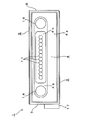
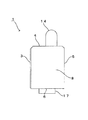
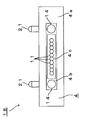
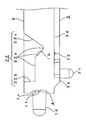
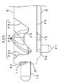
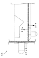
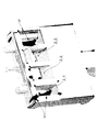
図7は、本実施形態におけるレンズアレイ(レンズアレイ本体)18を示す背面図であり、図8は、図7の平面図、図9は、図7のA-A断面図、図10は、図7のB-B断面図である。
本実施形態におけるレンズアレイ18は、図1乃至図5に示したものと同様に、金型を用いた樹脂材料の射出成形によって製造される。なお、樹脂材料としては、ポリエーテルイミド樹脂や環状オレフィン樹脂等を用いることができる。
また、図7乃至図10に示すように、本実施形態におけるレンズアレイ18は、図1乃至図5に示したものと同様に、第1の面としての上面4、第2の面としての前面3、第3の面としての背面5、第4の面としての底面6および左右の側面7、8を有している。
さらに、図7および図8に示すように、上面4は、従来と同様に、その中央に形成されたレンズアレイ18の横幅方向に沿って長尺な平面略長方形状の第2のザグリ平面4cと、この第2のザグリ平面4cを四方から包囲する枠状の第1のザグリ平面4bと、この第1のザグリ平面4bを四方から包囲する枠状の最上面4aとによって構成されている。そして、図7および図8に示すように、従来と同様に、第2のザグリ平面4cには、複数の第1のレンズ面11が、レンズアレイ18の横幅方向に整列するように形成されている。なお、各第1のレンズ面11は、互いに同径とされているとともに、形成ピッチが一定とされている。
さらにまた、図9および図10に示すように、本実施形態における前面3は、ザグリ面3dと、このザグリ面3dを四方から包囲する最前面3aとによって構成されている。そして、ザグリ面3dには、各第1のレンズ面11にそれぞれ対応する第1のレンズ面11と同数の複数の第2のレンズ面12が、第1のレンズ面11の整列方向すなわちレンズアレイ18の横幅方向に沿って整列するように形成されている。なお、第2のレンズ面12は、互いに同径とされているとともに、形成ピッチが一定とされている。また、互いに対応する第1のレンズ面11と第2のレンズ面12とは、整列方向における形成位置が互いに一致している。
なお、図9および図10からも分かるように、前面3は、上面4に対して第1のレンズ面11の整列方向に直交する一方の側において隣位する面となっている。また、背面5は、上面4に対して第1のレンズ面11の整列方向に直交する他方の側において隣位するとともに前面3に対向する面となっている。さらに、底面6は、上面4に対向する面となっている。
また、図7、図9および図10に示すように、背面5の図7における上半部の領域内であって、この領域におけるレンズアレイ18の横幅方向の中心位置に対して図7における左側の位置には、第1の全反射面19が凹入形成されている。この第1の全反射面19は、平面形状がレンズアレイ18の横幅方向に長尺な長方形状を呈しているとともに、前面3および上面4に対して所定の傾斜角を有する平坦な傾斜面に形成されている。傾斜角は、前面3および上面4のそれぞれに対して45°であってもよい。また、図7および図9に示すように、第1の全反射面19には、複数の第1のレンズ面11のうちの整列方向における一方(図7における左方)側から数えて所定数の第1のレンズ面11が上方において対向配置されているとともに、これら所定数の第1のレンズ面11に対応する所定数の第2のレンズ面12が前方(図9における下方)において対向配置されている。
このように形成された第1の全反射面19は、互いに対応する各第1のレンズ面11のそれぞれと各第2のレンズ面12のそれぞれとを結ぶ光路を形成する。例えば、第1の全反射面19に対応する各第2のレンズ面12に、各第2のレンズ面12における光軸と中心軸がそれぞれ一致するような同軸状の各光をレンズアレイ18の外側から入射させると、入射した各光は、レンズアレイ18の内部の光路上を第1の全反射面19側に向かって進行した後に、第1の全反射面19に臨界角以上の入射角で入射することになる。そして、第1の全反射面19に入射した各光は、第1の全反射面19に対応する各第1のレンズ面11側に全反射されることになる。そして、第1の全反射面19によって全反射された各光は、レンズアレイ18の内部の光路上を進行した後に、各第1のレンズ面11に、各光の中心軸を各第1のレンズ面11における光軸とそれぞれ一致させた状態で同軸状に入射することになる。このようにして、互いに対応する各第1のレンズ面11のそれぞれと各第2のレンズ面12のそれぞれとを結ぶ光路が第1の全反射面19によって形成される。このような光路は、第1の全反射面19およびこれに対応するレンズ面11、12を介してレンズアレイ18による光送信を行う場合の光路に相当する。なお、各第1のレンズ面11と同軸状の各光をレンズアレイ18の外側から各第1のレンズ面11に入射させた場合には、光送信の場合とは光の進行方向が逆転した状態の光路が形成されることになる。この場合の光路は、第1の全反射面19およびこれに対応するレンズ面11、12を介してレンズアレイ18による光受信を行う場合の光路に相当する。
さらに、図7、図9および図10に示すように、背面5の図7における上半部の領域内であって、この領域におけるレンズアレイ18の横幅方向の中心位置に対して図7における右側の位置には、第2の全反射面20が、第1の全反射面19に対して第1のレンズ11の整列方向すなわちレンズアレイ18の横幅方向に間隔を設けるようにして凹入形成されている。この第2の全反射面20も、第1の全反射面19と同様に、平面形状がレンズアレイ18の横幅方向に長尺な長方形状を呈しているとともに、前面3および上面4に対して所定の傾斜角を有する平坦な傾斜面に形成されている。傾斜角は、前面3および上面4のそれぞれに対して45°であってもよい。また、図7および図9に示すように、第2の全反射面20には、複数の第1のレンズ面11のうちの整列方向における他方(図7における右方)側から数えて所定数の第1のレンズ面11が上方において対向配置されているとともに、これら所定数の第1のレンズ面11に対応する所定数の第2のレンズ面12が前方(図9における下方)において対向配置されている。
このように形成された第2の全反射面20は、互いに対応する各第1のレンズ面11のそれぞれと各第2のレンズ面12のそれぞれとを結ぶ光路を形成する。例えば、第2の全反射面20に対応する各第1のレンズ面11に、同軸状の各光をレンズアレイ18の外側から入射させると、入射した各光は、レンズアレイ18の内部(但し、後述する第2のウエルド制御用凹部23がなす空間を含む)の光路上を第2の全反射面20側に向かって進行した後に、第2の全反射面20に臨界角以上の入射角で入射することになる。そして、第2の全反射面20に入射した各光は、第2の全反射面20に対応する各第2のレンズ面12側に全反射されることになる。そして、第2の全反射面20によって全反射された各光は、レンズアレイ18の内部の光路上を進行した後に、各第2のレンズ面12に同軸状に入射することになる。このようにして、互いに対応する各第1のレンズ面11のそれぞれと各第2のレンズ面12のそれぞれとを結ぶ光路が第2の全反射面20によって形成される。このような光路は、第2の全反射面20およびこれに対応するレンズ面11、12を介してレンズアレイ18による光受信を行う場合の光路に相当する。なお、各第2のレンズ面12と同軸状の各光をレンズアレイ18の外側から各第2のレンズ面12に入射させた場合には、光受信の場合とは光の進行方向が逆転した状態の光路が形成される。この場合の光路は、第2の全反射面20およびこれに対応するレンズ面11、12を介してレンズアレイ18による光送信を行う場合の光路に相当する。
さらにまた、図7に示すように、底面6には、従来と同様に、金型のゲート内において成形されるゲート部17が下方に向かって突出形成されている。
また、図7乃至図10に示すように、レンズアレイ18には、従来と同様に、複数の光ファイバおよび光電変換素装置の位置決め構造が形成されている。すなわち、図7乃至図10に示すように、上面4における第1のザグリ平面4bには、各第1のレンズ面11を挟んで左右一対の嵌合凸部14が形成されている。これらの嵌合凸部14は、従来と同様に、複数の光ファイバをレンズアレイ18に取り付ける際の各光ファイバの位置決めに用いられる。
一方、図9および図10に示すように、前面3における横幅方向の両端部近傍には、一対の嵌合凸部21がそれぞれ形成されている。これらの嵌合凸部21は、図1乃至図6に示した嵌合穴部10と同様に、光電変換素装置をレンズアレイ18に取り付ける際の光電変換素装置の位置決めに用いられる。ただし、本実施形態においては、光電変換素装置側の位置決め構造は、嵌合凸部21を嵌合させる嵌合穴部または嵌合孔となる。なお、光電変換装置に配置する光電変換素子は、第1の全反射面19に対応する各第2のレンズ面12に対しては、光送信用の発光素子を割り当て、第2の全反射面20に対応する各第2のレンズ面12に対しては、光受信用の受光素子を割り当ててもよい。
そして、このような構成に加えて、さらに、図7および図9に示すように、背面5の図7における上半部の領域内であって、この領域におけるレンズアレイ18の横幅方向の中心位置に対して図7における左側の位置には、第1のウエルド制御用凹部22が凹入形成されている。図7に示すように、第1のウエルド制御用凹部22は、底面22aおよびこの底面22aを四方から包囲する上下左右の側面22b~eからなる内面によって構成され、平面形状が上下に長尺な長方形状を呈している。また、図7および図9に示すように、底面22aには、第1の全反射面19が含まれている。さらに、第1のウエルド制御用凹部22は、その図7における上端部が、第1の全反射面19の上端部よりも上方の上面4の近傍に至る位置に形成されているとともに、その図7における下端部が、第1の全反射面19の下端部よりも下方の位置に形成されている。一方、第1のウエルド制御用凹部22の左端部は、第1の全反射面19の左端部とレンズアレイ18の横幅方向において同位置または僅かに左方に形成され、第1のウエルド制御用凹部22の右端部は、第1の全反射面19の右端部とレンズアレイ18の横幅方向において同位置または僅かに右方に形成されている。さらにまた、底面22aのうちの第1の全反射面19以外の部位は、互いに前後に段差を有するような背面5に平行な平坦面に形成されている。また、左右の側面22d、eは、レンズアレイ18の左右の側面7、8に平行な平坦面または前方(図7における紙面奥側)に向かうにしたがって互いに接近する方向に僅かに傾斜するような平坦面に形成されている。さらに、上側の側面22bは、後方に向かうにしたがって上方に僅かに傾斜するような傾斜面に形成されている。さらにまた、下側の側面22cは、後方に向かうにしたがって下方に傾斜するような傾斜面に形成されている。なお、図7においては、第1のウエルド制御用凹部22の内面のうち、上方に向かうにしたがって下り傾斜となる面については右斜め方向のハッチングが施され、背面5に平行な面については白抜きとされ、上方に向かうにしたがって上り傾斜となる面については左斜め方向のハッチングが施されている。
このような第1のウエルド制御用凹部22の設計上の三次元形状(換言すれば、金型形状)は、レンズアレイ18の成形の際に、ウエルドの形成位置を複数の第1のレンズ面11から外れた位置に制御する。
また、図7および図10に示すように、背面5の図7における上半部の領域内であって、この領域におけるレンズアレイ18の横幅方向の中心位置に対して図7における右側の位置には、第2のウエルド制御用凹部23が凹入形成されている。図7に示すように、第2のウエルド制御用凹部23は、レンズアレイ18の横幅方向において互いに連通された内側凹部23A、中間凹部23Bおよび外側凹部23Cによって構成されており、平面形状が略h字形状を呈している。
ここで、図7に示すように、内側凹部23Aは、第1のウエルド制御用凹部22と横幅がほぼ同一とされている。また、図7および図10に示すように、内側凹部23Aの底面23aには、第2の全反射面20が含まれている。さらに、内側凹部23Aの図7における上端部は、第2の全反射面20の上端部よりも上方の上面4の近傍に至る位置に形成されている。さらにまた、内側凹部23Aの図7における下端部は、第2の全反射面20の下端部よりも下方の位置に形成されているとともに、第1のウエルド制御用凹部22の下端部と上下方向において同一に形成されている。また、内側凹部23Aの左端部は、第2の全反射面20の左端部とレンズアレイ18の横幅方向において同位置または僅かに左方に形成されている。さらに、内側凹部23Aの右端部には、中間凹部23Bが連通されている。さらにまた、図10に示すように、内側凹部23Aの底面23aのうちの第2の全反射面20以外の部位は、背面5に平行な平坦面あるいは傾斜面に形成されている。また、内側凹部23Aの左右の側面は、レンズアレイ18の左右の側面7、8に平行な平坦面または前方に向かうにしたがって互いに接近する方向に僅かに傾斜するような平坦面に形成されている。さらに、内側凹部23Aの上側の側面23bは、後方に向かうにしたがって上方に傾斜するような傾斜面に形成されている。さらにまた、内側凹部23Aの下側の側面23cは、後方に向かうにしたがって下方に傾斜するような傾斜面に形成されている。なお、図7において、内側凹部23Aを構成する面のうち、上方に向かうにしたがって下り傾斜となる面については右斜め方向のハッチングが施され、背面5に平行な面については白抜きとされ、上方に向かうにしたがって上り傾斜となる面については左斜め方向のハッチングが施されている。
また、図7および図10に示すように、中間凹部23Bの図7における上端部は、第1のウエルド制御用凹部22の上端部と上下方向において同位置に形成されている。さらに、中間凹部23Bの図7における下端部は、内側凹部23Aの下端部よりも上方に形成されている。さらにまた、中間凹部23Bの底面23aは、背面5に平行な平坦面に形成されている。また、中間凹部23Bの上側の側面23bは、後方に向かうにしたがって上方に僅かに傾斜するような傾斜面に形成されている。さらに、中間凹部23Bの下側の側面23bは、後方に向かうにしたがって下方に傾斜するような傾斜面に形成されている。さらにまた、中間凹部23Bの右端部には、外側凹部23Cが連通されている。また、図7において、中間凹部23Bを構成する面のうち、上方に向かうにしたがって下り傾斜となる面については右斜め方向のハッチングが施され、背面5に平行な面については白抜きとされ、上方に向かうにしたがって上り傾斜となる面については左斜め方向のハッチングが施されている。
さらに、図7に示すように、外側凹部23Cの図7における上端部は、中間凹部23Bの上端部と上下方向において同位置に形成されている。さらにまた、外側凹部23Cの下端部は、第1のウエルド制御用凹部22の下端部と上下方向において同位置に形成されている。また、外側凹部23Cの底面23aは、背面5に平行な前後に段差を有する平坦面に形成され、左右の側面23d、eは、レンズアレイ18の左右の側面7、8に平行な平坦面に形成され、上下の側面23b、cは、上面4に平行な平坦面に形成されている。
このような第2のウエルド制御用凹部23の設計上の三次元形状(換言すれば、金型形状)は、レンズアレイ18の成形の際に、第1のウエルド制御用凹部22の設計上の三次元形状とともにウエルドの形成位置を複数の第1のレンズ面11から外れた位置に制御する。
ここで、図7、図9および図10からも分かるように、第1のウエルド制御用凹部22と第2のウエルド制御用凹部23とは互いに非鏡面対称な三次元形状に形成されている。
さらに、図7に示すように、ゲート部17は、その第1のレンズ面11の整列方向における中心位置を通り上面4に直交する仮想直線Lが、第1のウエルド制御用凹部22と第2のウエルド制御用凹部23との間、より具体的には、第1のウエルド制御用凹部22の右側面22eと内側凹部23Aの左側面23dとの中間位置を通るように形成されている。
さらにまた、図7に示すように、背面5の図7における上半部の領域内であって、第1のウエルド制御用凹部22に対して第1のレンズ面11の整列方向における外側(図7における左側)の位置には、第3のウエルド制御用凹部24が凹入形成されている。この第3のウエルド制御用凹部24は、底面24aおよび上下左右の側面24b~eによって構成され、平面形状が上下に長尺な長方形状を呈している。図7に示すように、第3のウエルド制御用凹部24の上端部は、第1のウエルド制御用凹部22の上端部と上下方向において同位置に形成されている。また、第3のウエルド制御用凹部24の下端部は、第1のウエルド制御用凹部22の下端部と上下方向において同位置に形成されている。さらに、底面24aは、背面5に平行な面一の平坦面に形成され、左右の側面24d、eは、レンズアレイ18の左右の側面7、8に平行な平坦面に形成され、上下の側面24b、cは、上面4に平行な平坦面に形成されている。
このような第3のウエルド制御用凹部24の設計上の三次元形状(換言すれば、金型形状)は、レンズアレイ18の成形の際に、第1のウエルド制御用凹部22および第2のウエルド制御用凹部23の設計上の三次元形状とともにウエルドの形成位置を複数の第1のレンズ面11から外れた位置に制御するようになっている。
なお、図7に示すように、本実施形態においては、第1のウエルド制御用凹部22および第2のウエルド制御用凹部23の形状に起因して、第1の全反射面19と第2の全反射面20との間に、第1のレンズ面11の整列方向の間隙部が形成されている。したがって、この間隙部に対応する位置に形成された第1のレンズ面11および第2のレンズ面12は、実質上、光学的に機能しないことになる。ただし、このような間隙部に対応する第1のレンズ面11および第2のレンズ面12を初めから形成しない設計も可能である。
また、本実施形態におけるレンズアレイ18は、例えば、図11に示すような上型27a(可動型)、下型27b(固定型)およびスライド型27c(可動型)からなる金型27を用いた樹脂材料の射出成形法によって一体的に形成することができる。ここで、上型27aは、第2のレンズ面12、嵌合凸部21、前面3およびゲート部17の前面の各形状を成形するための形状転写面を有している。また、下型27bは、第1の全反射面19を含む第1のウエルド制御用凹部22、第2の全反射面20を含む第2のウエルド制御用凹部23、第3のウエルド制御用凹部24、背面5、左右の側面7、8およびゲート部17の左右両側面ならびに背面の各形状を成形するための形状転写面を有している。さらに、スライド型27cは、第1のレンズ面11、嵌合凸部14および上面4の各形状を成形するための形状転写面を有している。前述のように、ゲート部17の形状転写面は、金型27のゲートを構成し、その他の形状転写面は、金型27のキャビティを構成する。なお、図11において、スプールおよびランナについては図示を省略している。また、上型27aは、更に、第2のレンズ面12およびこの周辺の形状を転写するレンズ駒と、このレンズ駒の外側に配置された枠駒とに分割されていてもよい。同様に、スライド型27cは、更に、第1のレンズ面11およびこの周辺の形状を転写するレンズ駒と、このレンズ駒の外側に配置された枠駒とに分割されていてもよい。
図12(a)~(c)は、このような本実施形態のレンズアレイ18を金型27を用いて樹脂成形する場合における溶融樹脂材料の流動過程を、レンズアレイ18の設計上の形状(金型形状)とともに示したものである。
図12(a)に示すように、本実施形態のレンズアレイ18によれば、その成形の際に、第1のウエルド制御用凹部22および第2のウエルド制御用凹部23の金型形状によって、両凹部22、23の内面のそれぞれと前面3との間に相当する金型27内の第1の空間S1を経由して金型27のゲートGから金型27内における第1のレンズ面11の形成位置P側に向かう溶融樹脂材料の第1の流れ(1)が、溶融樹脂材料の量的に抑制される。これは、特に、両凹部22、23における下側の側面22c、23cに相当する金型形状(形状転写面)22c’、23c’に第1の流れ(1)が突き当たって進行を制限されることによるものである。なお、第1の流れ(1)にしたがった溶融樹脂材料は、進行を制限されつつも、凹部22、23を潜るようにして形成位置P側に向かうことになる。
また、このとき、図12(a)に示すように、第3のウエルド制御用凹部24の金型形状によって、この凹部24の内面と前面3との間に相当する金型27内の第3の空間S3を経由してゲートGから第1のレンズ面11の形成位置P側に向かう溶融樹脂材料の第3の流れ(3)が量的に抑制される。これは、特に、第3のウエルド制御用凹部24における下側の側面24cに相当する金型形状24c’に第3の流れ(3)が突き当たって進行を制限されることによるものである。
このとき、図12(a)に示すように、第1のウエルド制御用凹部22および第2のウエルド制御用凹部23の金型形状によって、背面5における両凹部22、23に挟まれた部位と前面3との間に相当する金型27内の第2の空間S2を経由してゲートGから第1のレンズ面11の形成位置Pに至る溶融樹脂材料の中央側の流路が形成される。
ここで、この中央側の流路を流れる溶融樹脂材料の第2の流れ(2)は、第1の流れ(1)や第3の流れ(3)のように量的に抑制されてはおらず、また、ゲートGから第1のレンズ面11の形成位置Pに至る最短の流路長の流れである。したがって、第2の流れ(2)にしたがった溶融樹脂材料は、その大部分が、他の流れにしたがった溶融樹脂材料に先んじて第1のレンズ面11の形成位置Pに到達することになる。
そして、このようにして第1のレンズ面11の形成位置Pに到達した第2の流れ(2)にしたがった溶融樹脂材料は、形成位置Pにおける中央部において第1のレンズ面11の整列方向における両外側すなわち図12(a)における左右に分岐される。
これにより、図12(b)に示すような溶融樹脂材料の第4の流れ(4)および第5の流れ(5)が生じることになる。ここで、図12(b)に示すように、第4の流れ(4)にしたがった溶融樹脂材料は、第5の流れ(5)との分岐位置から左側に進行する過程で、その一部が、第1のレンズ面11の形状転写面のうちの左半部に中央側から順次充填されていく。また、このとき、図12(b)に示すように、第5の流れ(5)にしたがった溶融樹脂材料は、第4の流れ(4)との分岐位置から右側に進行する過程で、その一部が、第1のレンズ面11の形状転写面のうちの右半部に中央側から順次充填されていく。
そして、このようにして第4の流れ(4)および第5の流れ(5)にしたがった溶融樹脂材料が第1のレンズ面11の形成に主として関与する一方で、中央側の流路に対する第1のレンズ面11の整列方向の外側の流路から第1のレンズ面11の形成位置Pに流れ込もうとする溶融樹脂材料の大部分は、第4の流れ(4)および第5の流れ(5)が形成されていることによって、第1のレンズ面11の形成位置Pへの到達が手前で妨げられることになる。なお、外側の流路には、前述のような第1の流れ(1)および第3の流れ(3)をそれぞれ形成する流路、第1のウエルド制御用凹部22と第3のウエルド制御用凹部24との間の流路、第3のウエルド制御用凹部24の左外側の流路および第2のウエルド制御用凹部23の右外側の流路が含まれる。
これにより、図12(c)に示すように、中央の流路に対する外側の流路を流れる溶融樹脂材料(図中の破線矢印参照)は、第4の流れ(4)または第5の流れ(5)にしたがった溶融樹脂材料と、第1のレンズ面11の形成位置Pから外れた位置(手前)で合流することになる。
このような構成によれば、従来のように、第1のレンズ面11の形成位置において複数の溶融樹脂材料の流れが正面衝突に近い状態で会合するようなことはないため、第1のレンズ面11へのウエルドの形成を確実に回避することができる。
なお、第2のレンズ面12については、第1のレンズ面11に比べてゲートからの距離が相対的に短いため、ウエルドの問題は元々少ない。
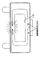
さらに、本実施形態におけるレンズアレイ18は、第1~第3のウエルド制御用凹部22、23、24の最適な三次元形状を樹脂材料の流動解析によって決定した上で、決定された三次形状の凹部22、23、24を転写する金型によって成形することができる。ここで、図13は、このような樹脂材料の流動解析方法の一例として、東レエンジニアリング株式会社製の樹脂流動解析ソフト(3D TIMON)(TIMONは同社の登録商標)を用いたポリイミド樹脂の流動解析結果を示したものである。
図13に示すように、本実施形態の第1~第3のウエルド制御用凹部22、23、24の三次元形状によれば、図中の斑模様に示されるウエルドWの形成位置を、第1のレンズ面11の形成位置から外れた位置に確実に制御できることが分かる。
以上述べたように、本実施形態によれば、第1、第2、第3のウエルド制御用凹部22、23、24により、ウエルドの形成位置を複数の第1のレンズ面11から外れた位置に制御することができるので、ゲート部17が底面6に形成された簡便なモジュール化に適した構成でありながら、第1のレンズ面11上へのウエルドの形成を回避して光学性能を確保することができる。
なお、本発明は前述した実施の形態に限定されるものではなく、必要に応じて種々変更することができる。
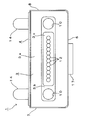
例えば、図14の変形例に示すように、第3のウエルド制御用凹部を備えず、第1のウエルド制御用凹部22および第2のウエルド制御用凹部23のみを備えるようにしてもよい。このような場合であっても、第1および第2のウエルド制御用凹部22、23によってウエルドの形成位置を複数の第1のレンズ面11から外れた位置に制御することにより、図7乃至図10に示した構成と同様の効果を奏することができる。
2010年4月9日出願の特願2010-090580の日本出願に含まれる明細書、図面および要約書の開示内容は、すべて本願に援用される。
3 前面
4 上面
5 背面
6 底面
11 第1のレンズ面
12 第2のレンズ面
17 ゲート部
19 第1の全反射面
20 第2の全反射面
22 第1のウエルド制御用凹部
23 第2のウエルド制御用凹部
4 上面
5 背面
6 底面
11 第1のレンズ面
12 第2のレンズ面
17 ゲート部
19 第1の全反射面
20 第2の全反射面
22 第1のウエルド制御用凹部
23 第2のウエルド制御用凹部
Claims (5)
- 金型を用いて成形された樹脂材料からなるレンズアレイであって、
レンズアレイ本体における第1の面に、所定の整列方向に整列するように形成された複数の第1のレンズ面と、
前記第1の面に前記整列方向に直交する一方の側において隣位する前記レンズアレイ本体における第2の面に、前記整列方向に沿って整列するように形成された複数の第2のレンズ面と、
前記第1の面に前記第1のレンズ面の整列方向に直交する他方の側において隣位するとともに前記第2の面に対向する前記レンズアレイ本体における第3の面に凹入形成され、前記複数の第1のレンズ面のうちの前記整列方向における一方側から数えて所定数の第1のレンズ面のそれぞれとこれらに対応する所定数の前記第2のレンズ面のそれぞれとを結ぶ光路を形成する第1の全反射面と、
前記第3の面に、前記第1の全反射面に対して前記整列方向に所定の間隔を設けるようにして凹入形成され、前記複数の第1のレンズ面のうちの前記整列方向における他方側から数えて所定数の第1のレンズ面のそれぞれとこれらに対応する所定数の前記第2のレンズ面のそれぞれとを結ぶ光路を形成する第2の全反射面と、
前記第3の面に、前記第1の全反射面を底面に含むようにして凹入形成され、前記レンズアレイ本体の成形の際にウエルドの形成位置を前記複数の第1のレンズ面から外れた位置に制御可能な三次元形状を有する第1のウエルド制御用凹部と、
前記第3の面に、前記第2の全反射面を底面に含むとともに、前記第1のウエルド制御用凹部に対して前記整列方向に所定の間隔を設けるようにして凹入形成され、前記レンズアレイ本体の成形の際に前記第1のウエルド制御用凹部の三次元形状とともに前記ウエルドの形成位置を前記複数の第1のレンズ面から外れた位置に制御可能な三次元形状を有する第2のウエルド制御用凹部と、
前記第1の面に対向する前記レンズアレイ本体における第4の面に形成されたゲート部と、
を備え、
前記ゲート部は、その前記整列方向における中心位置を通り前記第1の面に直交する仮想直線が前記第1のウエルド制御用凹部と前記第2のウエルド制御用凹部との間を通るように形成され、
前記第1のウエルド制御用凹部および前記第2のウエルド制御用凹部の三次元形状は、
前記レンズアレイ本体の成形の際に、これら両凹部の内面のそれぞれと前記第2の面との間に相当する前記金型内の第1の空間を経由して前記金型のゲートから前記金型内における前記第1のレンズ面の形成位置側に向かう溶融樹脂材料の流れを抑制する形状であり、かつ、
前記第3の面における前記両凹部に挟まれた部位と前記第2の面との間に相当する前記金型内の第2の空間を経由して前記ゲートから前記第1のレンズ面の形成位置に至る溶融樹脂材料の中央側の流路が形成され、この中央側の流路を流れる溶融樹脂材料を、前記第1のレンズ面の形成位置に到達させた上でこの第1のレンズ面の形成位置において前記整列方向における両外側に分岐させ、分岐させた後の溶融樹脂材料を、前記中央側の流路に対する前記整列方向の外側の流路から前記第1のレンズ面の形成位置に流れ込もうとする溶融樹脂材料と前記第1のレンズ面の形成位置から外れた位置において合流させる形状である、
レンズアレイ。 - 前記第1のウエルド制御用凹部と前記第2のウエルド制御用凹部とは、互いに非鏡面対称に形成されている、請求項1に記載のレンズアレイ。
- 前記第3の面における前記第1のウエルド制御用凹部および前記第2のウエルド制御用凹部の少なくとも一方に対する前記整列方向の外側位置に凹入形成され、前記レンズアレイ本体の成形の際に前記第1のウエルド制御用凹部および前記第2のウエルド制御用凹部の三次元形状とともに前記ウエルドの形成位置を前記複数の第1のレンズ面から外れた位置に制御可能な三次元形状を有する少なくとも1つの第3のウエルド制御用凹部を備え、
前記第3のウエルド制御用凹部の三次元形状は、前記レンズアレイ本体の成形の際に、この凹部の内面と前記第2の面との間に相当する前記金型内の第3の空間を経由して前記ゲートから前記第1のレンズ面の形成位置側に向かう溶融樹脂材料の流れを抑制する形状である、
請求項1に記載のレンズアレイ。 - 請求項1に記載のレンズアレイを製造するために、
樹脂材料の流動解析によって前記第1のウエルド制御用凹部および前記第2のウエルド制御用凹部のそれぞれの三次元形状を決定し、決定された三次元形状を有する前記各ウエルド制御用凹部を備えた前記レンズアレイを製造する、レンズアレイの製造方法。 - 請求項3に記載のレンズアレイを製造するために、
樹脂材料の流動解析によって前記第1のウエルド制御用凹部、前記第2のウエルド制御用凹部および前記第3のウエルド制御用凹部のそれぞれの三次元形状を決定し、決定された三次元形状を有する前記各ウエルド制御用凹部を備えた前記レンズアレイを製造する、レンズアレイの製造方法。
Applications Claiming Priority (2)
| Application Number | Priority Date | Filing Date | Title |
|---|---|---|---|
| JP2010090580A JP2013127491A (ja) | 2010-04-09 | 2010-04-09 | レンズアレイおよびその製造方法 |
| JP2010-090580 | 2010-04-09 |
Publications (1)
| Publication Number | Publication Date |
|---|---|
| WO2011125341A1 true WO2011125341A1 (ja) | 2011-10-13 |
Family
ID=44762308
Family Applications (1)
| Application Number | Title | Priority Date | Filing Date |
|---|---|---|---|
| PCT/JP2011/002106 Ceased WO2011125341A1 (ja) | 2010-04-09 | 2011-04-08 | レンズアレイおよびその製造方法 |
Country Status (2)
| Country | Link |
|---|---|
| JP (1) | JP2013127491A (ja) |
| WO (1) | WO2011125341A1 (ja) |
Cited By (3)
| Publication number | Priority date | Publication date | Assignee | Title |
|---|---|---|---|---|
| WO2012077762A1 (ja) * | 2010-12-09 | 2012-06-14 | 株式会社エンプラス | レンズアレイおよびその製造方法 |
| JP2013137448A (ja) * | 2011-12-28 | 2013-07-11 | Sumitomo Electric Ind Ltd | レンズ部品 |
| WO2019059096A1 (ja) * | 2017-09-25 | 2019-03-28 | 株式会社エンプラス | 光レセプタクルの製造方法およびそれに用いる金型 |
Families Citing this family (1)
| Publication number | Priority date | Publication date | Assignee | Title |
|---|---|---|---|---|
| JP6291300B2 (ja) | 2014-03-19 | 2018-03-14 | 株式会社エンプラス | 光レセプタクルおよび光モジュール |
Citations (4)
| Publication number | Priority date | Publication date | Assignee | Title |
|---|---|---|---|---|
| JPH0752199A (ja) * | 1993-08-10 | 1995-02-28 | Oki Electric Ind Co Ltd | ウエルドマークの位置制御方法 |
| JP2005031556A (ja) * | 2003-07-10 | 2005-02-03 | Omron Corp | 光路変換型光結合素子 |
| JP2005288734A (ja) * | 2004-03-31 | 2005-10-20 | Nippon A & L Kk | ウエルドラインを任意の位置に調整可能な成形品の成形方法およびそれにより得られた成形品 |
| JP2009163212A (ja) * | 2007-12-12 | 2009-07-23 | Enplas Corp | 光結合素子およびこれを備えた光モジュール |
-
2010
- 2010-04-09 JP JP2010090580A patent/JP2013127491A/ja active Pending
-
2011
- 2011-04-08 WO PCT/JP2011/002106 patent/WO2011125341A1/ja not_active Ceased
Patent Citations (5)
| Publication number | Priority date | Publication date | Assignee | Title |
|---|---|---|---|---|
| JPH0752199A (ja) * | 1993-08-10 | 1995-02-28 | Oki Electric Ind Co Ltd | ウエルドマークの位置制御方法 |
| JP2005031556A (ja) * | 2003-07-10 | 2005-02-03 | Omron Corp | 光路変換型光結合素子 |
| JP2005288734A (ja) * | 2004-03-31 | 2005-10-20 | Nippon A & L Kk | ウエルドラインを任意の位置に調整可能な成形品の成形方法およびそれにより得られた成形品 |
| JP2009163212A (ja) * | 2007-12-12 | 2009-07-23 | Enplas Corp | 光結合素子およびこれを備えた光モジュール |
| JP2009163213A (ja) * | 2007-12-12 | 2009-07-23 | Enplas Corp | 光結合素子およびこれを備えた光モジュール |
Cited By (5)
| Publication number | Priority date | Publication date | Assignee | Title |
|---|---|---|---|---|
| WO2012077762A1 (ja) * | 2010-12-09 | 2012-06-14 | 株式会社エンプラス | レンズアレイおよびその製造方法 |
| US9164267B2 (en) | 2010-12-09 | 2015-10-20 | Enplas Corporation | Lens array and manufacturing method thereof |
| JP2013137448A (ja) * | 2011-12-28 | 2013-07-11 | Sumitomo Electric Ind Ltd | レンズ部品 |
| WO2019059096A1 (ja) * | 2017-09-25 | 2019-03-28 | 株式会社エンプラス | 光レセプタクルの製造方法およびそれに用いる金型 |
| JP2019060978A (ja) * | 2017-09-25 | 2019-04-18 | 株式会社エンプラス | 光レセプタクルの製造方法およびそれに用いる金型 |
Also Published As
| Publication number | Publication date |
|---|---|
| JP2013127491A (ja) | 2013-06-27 |
Similar Documents
| Publication | Publication Date | Title |
|---|---|---|
| CN102667565B (zh) | 透镜阵列以及具备该透镜阵列的光学模块 | |
| JP6746074B2 (ja) | 光学モジュールデバイスおよびこれを製造する方法 | |
| JP5127546B2 (ja) | 光コネクタ | |
| JP5896098B2 (ja) | レンズアレイ | |
| TWI611230B (zh) | 光插座以及光模組 | |
| US20050058399A1 (en) | Optical waveguide structure and optical module | |
| KR20260044253A (ko) | 광 섬유 대 칩 광 커플러 | |
| JP5292184B2 (ja) | 光モジュール及びその製造方法 | |
| WO2013062004A1 (ja) | レンズアレイおよびその製造方法 | |
| JP2017156630A (ja) | 光レセプタクル、光モジュールおよび光モジュールの製造方法 | |
| JP5550353B2 (ja) | レンズアレイおよびこれを備えた光モジュール | |
| WO2011125341A1 (ja) | レンズアレイおよびその製造方法 | |
| JPWO2018042984A1 (ja) | 光接続構造 | |
| US10094993B2 (en) | Connector and connector set with asymmetric coupled surfaces | |
| JP2016145907A (ja) | 光導波路モジュール | |
| JP4894579B2 (ja) | レンズ筐体及び光モジュール | |
| CN107430246B (zh) | 光传输模块 | |
| WO2018105287A1 (ja) | 光レセプタクル、光モジュールおよび光モジュールの製造方法 | |
| JP6011908B2 (ja) | 光レセプタクルおよびこれを備えた光モジュール | |
| TW202210886A (zh) | 光連接器及光連接器模組 | |
| JP2017161579A (ja) | 光レセプタクルおよび光モジュール | |
| JP2007156114A (ja) | 光信号入出力装置の製造方法 | |
| US20260063855A1 (en) | Optical receptacle and optical module | |
| JP6475911B2 (ja) | 光コネクタ保持具、光コネクタモジュール、光学基板モジュール及び光モジュール | |
| US20130064511A1 (en) | Optical module and method of manufacturing the same |
Legal Events
| Date | Code | Title | Description |
|---|---|---|---|
| 121 | Ep: the epo has been informed by wipo that ep was designated in this application |
Ref document number: 11765243 Country of ref document: EP Kind code of ref document: A1 |
|
| NENP | Non-entry into the national phase |
Ref country code: DE |
|
| 122 | Ep: pct application non-entry in european phase |
Ref document number: 11765243 Country of ref document: EP Kind code of ref document: A1 |
|
| NENP | Non-entry into the national phase |
Ref country code: JP |