WO2011122076A1 - 液晶表示素子、およびその製造方法、ならびに当該液晶表示素子を備えた液晶表示装置 - Google Patents
液晶表示素子、およびその製造方法、ならびに当該液晶表示素子を備えた液晶表示装置 Download PDFInfo
- Publication number
- WO2011122076A1 WO2011122076A1 PCT/JP2011/051121 JP2011051121W WO2011122076A1 WO 2011122076 A1 WO2011122076 A1 WO 2011122076A1 JP 2011051121 W JP2011051121 W JP 2011051121W WO 2011122076 A1 WO2011122076 A1 WO 2011122076A1
- Authority
- WO
- WIPO (PCT)
- Prior art keywords
- liquid crystal
- substrate
- display area
- spacers
- display
- Prior art date
- Legal status (The legal status is an assumption and is not a legal conclusion. Google has not performed a legal analysis and makes no representation as to the accuracy of the status listed.)
- Ceased
Links
Images



Classifications
-
- G—PHYSICS
- G02—OPTICS
- G02F—OPTICAL DEVICES OR ARRANGEMENTS FOR THE CONTROL OF LIGHT BY MODIFICATION OF THE OPTICAL PROPERTIES OF THE MEDIA OF THE ELEMENTS INVOLVED THEREIN; NON-LINEAR OPTICS; FREQUENCY-CHANGING OF LIGHT; OPTICAL LOGIC ELEMENTS; OPTICAL ANALOGUE/DIGITAL CONVERTERS
- G02F1/00—Devices or arrangements for the control of the intensity, colour, phase, polarisation or direction of light arriving from an independent light source, e.g. switching, gating or modulating; Non-linear optics
- G02F1/01—Devices or arrangements for the control of the intensity, colour, phase, polarisation or direction of light arriving from an independent light source, e.g. switching, gating or modulating; Non-linear optics for the control of the intensity, phase, polarisation or colour
- G02F1/13—Devices or arrangements for the control of the intensity, colour, phase, polarisation or direction of light arriving from an independent light source, e.g. switching, gating or modulating; Non-linear optics for the control of the intensity, phase, polarisation or colour based on liquid crystals, e.g. single liquid crystal display cells
- G02F1/133—Constructional arrangements; Operation of liquid crystal cells; Circuit arrangements
- G02F1/1333—Constructional arrangements; Manufacturing methods
- G02F1/1339—Gaskets; Spacers; Sealing of cells
- G02F1/13394—Gaskets; Spacers; Sealing of cells spacers regularly patterned on the cell subtrate, e.g. walls, pillars
-
- G—PHYSICS
- G02—OPTICS
- G02F—OPTICAL DEVICES OR ARRANGEMENTS FOR THE CONTROL OF LIGHT BY MODIFICATION OF THE OPTICAL PROPERTIES OF THE MEDIA OF THE ELEMENTS INVOLVED THEREIN; NON-LINEAR OPTICS; FREQUENCY-CHANGING OF LIGHT; OPTICAL LOGIC ELEMENTS; OPTICAL ANALOGUE/DIGITAL CONVERTERS
- G02F1/00—Devices or arrangements for the control of the intensity, colour, phase, polarisation or direction of light arriving from an independent light source, e.g. switching, gating or modulating; Non-linear optics
- G02F1/01—Devices or arrangements for the control of the intensity, colour, phase, polarisation or direction of light arriving from an independent light source, e.g. switching, gating or modulating; Non-linear optics for the control of the intensity, phase, polarisation or colour
- G02F1/13—Devices or arrangements for the control of the intensity, colour, phase, polarisation or direction of light arriving from an independent light source, e.g. switching, gating or modulating; Non-linear optics for the control of the intensity, phase, polarisation or colour based on liquid crystals, e.g. single liquid crystal display cells
- G02F1/133—Constructional arrangements; Operation of liquid crystal cells; Circuit arrangements
- G02F1/1333—Constructional arrangements; Manufacturing methods
- G02F1/133388—Constructional arrangements; Manufacturing methods with constructional differences between the display region and the peripheral region
Definitions
- the present invention relates to a liquid crystal display element, a manufacturing method thereof, and a liquid crystal display device including the liquid crystal display element. More specifically, at least one of a pair of substrates constituting the liquid crystal display element is flexible.
- the present invention relates to a liquid crystal display element having the same, a manufacturing method thereof, and a liquid crystal display device including the liquid crystal display element.
- FPD thin flat panel display
- Some FPDs use liquid crystal, light emitting diodes (LEDs), organic electroluminescence (organic EL), or the like as display elements.
- LEDs light emitting diodes
- organic EL organic electroluminescence
- research and development of display devices using liquid crystals have been actively conducted because of the advantages of thinness, light weight, and low power consumption.
- a liquid crystal display device includes a backlight and a liquid crystal display element, and includes a surface light source device as a backlight and a liquid crystal panel as a liquid crystal display element.
- the liquid crystal panel is configured by enclosing liquid crystal between a rear substrate including a thin film transistor (TFT), a pixel electrode, an alignment film, and the like and a front substrate including a color filter, a counter electrode, an alignment film, and the like.
- TFT thin film transistor
- a frame-shaped seal is used to bond the front substrate and the rear substrate.
- the seal functions as an adhesive that bonds the substrates together and the liquid crystal injected between the substrates leaks out of the substrate. It has a role as a sealant for sealing so that there is no.
- a liquid crystal dropping method (ODF method) is adopted as a liquid crystal supply method.
- ODF method a liquid crystal dropping method
- a seal is applied on the front substrate in a frame shape, and then a liquid crystal is dropped into the frame by a certain amount using a dispenser to form a liquid crystal layer.
- Patent Documents 1 and 2 propose a device for maintaining the cell gap of the liquid crystal panel more effectively and uniformly.
- Patent Document 1 discloses a method of manufacturing a liquid crystal display element by sealing a liquid crystal injection port in a state where a pair of substrates into which liquid crystal has been injected is pressurized in a direction perpendicular to the substrate surface. Specifically, a pair of substrates coated with a seal are overlapped and uniformly pressurized in a direction perpendicular to the substrate surface. The seal is cured while the substrate is kept pressurized, and liquid crystal is injected from the liquid crystal injection port to seal the liquid crystal injection port. According to this, when sealing the liquid crystal injection port, excess liquid crystal injected between the substrates is discharged from the liquid crystal injection port, and the expansion of the gap between the substrates generated at the time of liquid crystal injection is corrected, and the gap is uniform. It becomes. At the same time, since the liquid crystal injection port is sealed in this state, the uniform gap can be maintained stably thereafter.
- Patent Document 2 discloses a liquid crystal display element in which a column spacer is provided in a liquid crystal cell. Specifically, column spacers that protrude toward the other substrate are formed on one of the pair of substrates. According to this, since the area of the portion in contact with the substrate is large, the column spacer is relatively strongly bonded between the two substrates. In addition, since the column spacer can be freely adjusted in position, both substrates can be uniformly bonded over the whole. Thereby, the cell gap of the liquid crystal panel is stably maintained, and particularly when the liquid crystal panel is bent, the cell gap is stably maintained.
- Japanese Patent Publication Japanese Patent Laid-Open No. 2001-075111” (published on March 23, 2001) Japanese Patent Publication “Japanese Patent Laid-Open No. 2006-338011 (Released on December 14, 2006)”
- Patent Documents 1 and 2 described above are difficult to apply to a liquid crystal display device employing a flexible substrate.
- the liquid crystal display element manufacturing method disclosed in Patent Document 1 described above is difficult to apply to a flexible substrate having no rigidity in consideration of handling during the manufacturing process. Therefore, it is difficult to realize the manufacture of a liquid crystal display element having a flexible substrate with a uniform cell gap using the manufacturing method disclosed in this document. Further, in this document, a conventional vacuum injection method is assumed as a method for forming a liquid crystal layer, and the manufacturing process is complicated, so that a manufacturing method with higher productivity is desired.
- the present invention has been made in view of the above problems, and its object is to provide a liquid crystal display element capable of maintaining a uniform and stable liquid crystal cell gap even when a flexible substrate is used, a manufacturing method thereof, and It is providing the liquid crystal display device provided with the said liquid crystal display element.
- a liquid crystal display element includes a liquid crystal layer provided between a pair of substrates, at least one of which is flexible, and the liquid crystal layer enclosed between the pair of substrates. And a seal for adhering between the pair of substrates, the liquid crystal display element comprising a plurality of spacers disposed in the liquid crystal layer and in contact with the pair of substrates, A region where one of the substrates is in contact with the liquid crystal layer is divided into a display region and a non-display region surrounding the display region, and compared with the number of spacers arranged per unit area of the non-display region. The number of the spacers arranged per unit area of the display region is large.
- the display area has a larger number of spacers arranged per unit area than the non-display area.
- the arrangement density of the spacers is different between the display area and the non-display area, and the arrangement density of the display area is higher than that of the non-display area.
- the non-display area functions as a buffer, deforms according to the amount of liquid crystal to be distributed, and makes the cell gap of the display area uniform and stable regardless of the amount of liquid crystal sealed in the liquid crystal display element. Can be maintained.
- the liquid crystal display device is characterized by including any one of the liquid crystal display elements described above and a backlight in order to solve the above-described problems.
- a liquid crystal layer provided between the first substrate and the second substrate, and the liquid crystal layer are combined with the first substrate and the above
- a liquid crystal display element manufacturing method comprising: a seal for sealing between the first substrate and the second substrate; and a display region on the first substrate; A spacer forming step of forming a plurality of spacers in a non-display region surrounding the display region, and the seal on the surface of the first substrate on which the plurality of spacers are formed so as to surround the plurality of spacers.
- a liquid crystal display element capable of maintaining a cell gap in the display region uniformly and stably can be provided.
- the non-display area is deformed by receiving the pressure.
- the non-display area functions as a buffer, and the cell gap in the display area can be maintained uniformly and stably regardless of the amount of liquid crystal sealed in the liquid crystal display element.
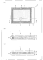
- (A) in a figure is a figure which shows the upper surface of the liquid crystal panel which concerns on one Embodiment of this invention
- (b) in the figure shows the cross section in one area
- (C) in the figure is a diagram showing a cross section in a region of the liquid crystal panel according to one embodiment of the present invention. It is a figure which shows the upper surface of the liquid crystal panel which concerns on one Embodiment of this invention. It is a figure which shows the variation
- a liquid crystal display device includes a backlight and a liquid crystal display element, and includes a surface light source device as a backlight and a liquid crystal panel as a liquid crystal display element.
- the liquid crystal panel according to the present embodiment will be described with reference to FIG.
- FIG. 1A is a view showing the upper surface of the liquid crystal panel 9.
- (B) in FIG. 1 is a view showing an AA ′ cross section in the region 7 shown in (a) in FIG.
- (C) in FIG. 1 is a view showing an AA ′ cross section in the region 8 shown in (a) in FIG.
- the liquid crystal panel 9 includes a pair of substrates (a front substrate 1a and a back substrate 1b) (a first substrate and a second substrate), and a liquid crystal layer provided between the substrates. 3 is provided.
- a frame-shaped seal 4 is used for bonding the front substrate 1a and the back substrate 1b.
- the seal 4 serves as an adhesive for bonding the substrates together, and liquid crystal injected between the substrates is a substrate. It has a role as a sealant for sealing so as not to leak to the outside.
- the region in contact with the liquid crystal layer 3 is divided into a non-display region 5 and a display region 6.
- a plurality of spacers 2 are formed in the non-display area 5 at intervals.
- a plurality of spacers 2 are also formed in the display area 6 at intervals.
- the plurality of spacers 2 formed in the non-display area 5 are formed with a larger interval between the adjacent spacers 2 than the plurality of spacers 2 formed in the display area 6. That is, compared to the non-display area 5, the number of spacers 2 arranged per unit area of the display area 6 is large.
- the spacer 2 is a columnar spacer formed by a photolithography method or the like, or a spherical spacer dispersed by an ink jet method or the like.
- the shape thereof is not particularly limited, and may be a columnar shape or a prismatic shape.
- the spacer 2 is formed by a method in which the arrangement position can be controlled, and has a role of keeping the distance between the front substrate 1a and the rear substrate 1b (that is, the liquid crystal cell gap 10) constant. Details will be described later.
- transparent electrodes such as an indium tin oxide (ITO) film are formed on surfaces facing each other (hereinafter referred to as an inner surface). It is sufficient that at least one of the front substrate 1a and the back substrate 1b is substantially transparent, and a glass substrate, a ceramic substrate, a plastic substrate, or the like can be used.
- ITO indium tin oxide
- Plastic substrates include cellulose derivatives such as cellulose, triacetyl cellulose, or diacetyl cellulose, polycycloolefin derivatives, polyesters such as polyethylene terephthalate or polyethylene naphthalate, polyolefins such as polypropylene or polyethylene, polycarbonate, polyvinyl alcohol, polychlorinated Vinyl, polyvinylidene chloride, polyamide, polyimide, polyimide amide, polystyrene, polyacrylate, polymethyl methacrylate, polyether sulfone, polyarylate, and inorganic and organic compounds such as glass fiber-epoxy resin, glass fiber-acrylic resin, etc.
- a composite material or the like can be used.
- the material is not particularly limited as long as at least one of the front substrate 1a and the rear substrate 1b has flexibility.
- the front substrate 1a and the rear substrate 1b are made of glass substrates, it is included in this embodiment as long as at least one of the glass substrates has flexibility.
- a simple matrix driving method or an active matrix driving method can be adopted.
- conductive wiring, switching elements, insulating films, and the like are appropriately formed on the inner surfaces of the front substrate 1a and the rear substrate 1b.
- an alignment film subjected to alignment treatment is formed at the interface between the two substrates and the liquid crystal layer 3 as necessary.
- a color filter is provided on the inner surface of the front substrate 1a and the outer surface (inner surface) of at least one of the front substrate 1a and the rear substrate 1b.
- a polarizing plate or the like is provided on the opposite side of the surface.
- the liquid crystal panel 9 is attached with a surface light source device as a backlight for illuminating the liquid crystal panel 9 or a reflector. Since these configurations are the same as those of a conventional liquid crystal display device, they are not mentioned here.
- the plurality of spacers 2 are formed in the liquid crystal layer 3 in order to keep the cell gap 10 of the liquid crystal constant.
- the present embodiment is characterized in that the arrangement density of the plurality of spacers 2 (the number of spacers 2 arranged per unit area) differs depending on the location. More specifically, the arrangement density of the spacers 2 in the non-display area 5 is relatively low, and the arrangement density of the spacers 2 in the display area 6 is relatively high. As a result, the cell gap 10 in the display region 6 becomes less susceptible to the amount of liquid crystal supplied, and the appropriate cell gap 10 can be stably maintained.
- FIG. 2 is a view showing the upper surface of the liquid crystal panel 29 in which the region surrounded by the seal 24 is divided into eight regions on the front substrate 21a or the rear substrate 21b.
- the region surrounded by the seal 24 is divided into eight regions (A to H), and the spacers 2 are formed so that the arrangement density and size of the spacers 2 are different for each region.
- Table 1 shows the arrangement density and size of the spacers 2 formed for each region.
- the size of the spacer 2 here is an area where the spacer 2 contacts the front substrate 21a or the rear substrate 21b.
- the region I in Table 1 is a region in a conventional liquid crystal panel using the same type of spacer 2 as the spacer 2 formed in the region B.
- the configuration of the liquid crystal panel 29 conforms to the liquid crystal panel 9 according to the present embodiment, and includes the same members as the liquid crystal panel 9.
- the front substrate 21a and the rear substrate 21b are film substrates made of a composite material of glass fiber and acrylic resin, and the thickness thereof is 100 ⁇ m.
- a transparent electrode, a columnar spacer 2, and an alignment film are sequentially formed on the inner surfaces of both substrates.
- a liquid crystal layer in which twisted nematic (TN) liquid crystal is sealed with a seal 24 is formed between the front substrate 21a and the back substrate 21b.
- TN twisted nematic
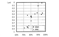
- FIG. 3 and FIG. 4 show the fluctuation amount of the liquid crystal cell gap 10 when the amount of liquid crystal to be sealed is changed in the liquid crystal panel 29.
- the vertical axis indicates the amount of fluctuation obtained by subtracting the cell gap 10 from the height of the spacer 2 in a no-load state when the liquid crystal is sealed by the liquid crystal dropping method (ODF method).
- the horizontal axis represents the ratio of the amount of liquid crystal sealed to the design cell volume.
- the design cell volume referred to here is the product of the area of the region in which the liquid crystal is sealed (the region surrounded by the seal 24) and the height of the spacer 2 in a no-load state. Note that all the measurements in the region other than the region I are performed in a liquid crystal cell that does not contain vacuum bubbles.
- the region I has a configuration in which the spacers 2 having the same arrangement density and size as the spacers 2 formed in the region B are formed in the liquid crystal cell.
- the cell gap 10 changes for each liquid crystal amount to be sealed.
- the amount of liquid crystal changes by 5% with respect to the set cell volume
- a fluctuation of 0.22 ⁇ m occurs in the cell gap 10. From this, it can be seen that in order to maintain a constant cell gap 10, it is important to accurately control the amount of liquid crystal to be supplied and the design cell volume.
- the flexible substrate does not have rigidity, the cell gap 10 varies due to bending or undulation. As a result, the display quality of the liquid crystal panel is degraded.
- the variation amount of the cell gap 10 for each liquid crystal amount to be sealed is small.
- the fluctuation amount of the cell gap 10 is reduced to 1/10 of the region I, and is a substantially constant value regardless of the amount of liquid crystal supplied. Therefore, the cell gap 10 can be kept substantially constant even when the amount of liquid crystal supplied changes. The reason will be described in detail below.
- the liquid crystal supplied to the liquid crystal panel 29 is first distributed preferentially to the regions A, B, E, and F. Thereafter, as the amount of liquid crystal supplied increases, liquid crystal that becomes excessive in the regions A, B, E, and F flows into the regions C, D, G, and H. As described above, the regions C, D, G, and H where the arrangement density of the spacers 2 is low have a function as a buffer for maintaining the cell gap 10 in the regions A, B, E, and F uniformly and stably. Yes.
- FIG. 5 is a diagram simply showing the direction of the atmospheric pressure applied to the liquid crystal panel 9.
- B in FIG. 5 is a view showing a cross section of the non-display area 5 in the case where the same amount of liquid crystal as the design cell volume is sealed.
- C in FIG. 5 is a diagram showing a cross section of the display region 6 in a case where the same amount of liquid crystal as the design cell volume is sealed.
- D in FIG. 5 is a diagram showing a cross section of the non-display area 5 in the case where a liquid crystal of an amount smaller than the design cell volume is sealed.
- E in FIG. 5 is a diagram showing a cross section of the display region 6 in a case where a liquid crystal of an amount smaller than the design cell volume is sealed.
- the arrangement density of the spacers 2 in the non-display area 5 is relatively low, and the arrangement density of the spacers 2 in the display area 6 is relatively high.
- the liquid crystal panel 9 after the front substrate 1a and the rear substrate 1b are bonded to each other corresponds to the volume of the difference between the design cell volume and the volume of the encapsulated liquid crystal. Pressure is evenly applied from the atmosphere (from the direction of the arrow).
- the design cell volume and the volume of the sealed liquid crystal are the same. No pressure from the atmosphere. This is not related to the arrangement density of the spacers 2. Therefore, the cell gap 10 of the non-display area 5 shown in FIG. 5B and the cell gap 10 of the display area 6 shown in FIG. 5C are equivalent. Therefore, in the above case, the uniform and stable cell gap 10 can be maintained also in the non-display area 5 and the display area 6.
- the design cell volume and the volume of the enclosed liquid crystal are stored in the liquid crystal panel 9.
- the pressure corresponding to the difference volume is applied from the atmosphere.
- the same pressure is applied to both the non-display area 5 shown in FIG. 5D and the display area 6 shown in FIG.
- the arrangement density of the spacers 2 is low in the non-display area 5
- the amount of compression of the spacers 2 due to the atmospheric pressure is larger than that in the display area 6 where the arrangement density of the spacers 2 is high.
- the cell gap 10 of the non-display area 5 shown in (d) of FIG. 5 is smaller than the cell gap 10 of the display area 6 shown in (e) of FIG.
- the installation interval of the spacers 2 is larger than the installation interval of the spacers 2 in the display area 6. For this reason, the degree of bending of the entire non-display area 5 is also increased. As a result, the amount of liquid crystal per unit area in the non-display area 5 is smaller than the amount of liquid crystal per unit area in the display area 6.
- the region where the arrangement density of the spacers 2 is high receives the pressure. Will be transformed.
- the region where the arrangement density of the spacers 2 is high receives the pressure. Will be transformed.
- the region where the arrangement density of the spacers 2 is high receives the pressure. Will be transformed.
- the region where the arrangement density of the spacers 2 is high receives the pressure. Will be transformed.
- the region where the arrangement density of the spacers 2 is high the cell gap 10 is maintained unchanged.
- the region where the spacer 2 is disposed at a low density functions as a buffer.
- the volume can be easily changed with respect to the change of the amount of liquid crystal using the flexibility of the flexible substrate.
- the flexible substrate (front substrate 1a and back substrate 1b) is 100 ⁇ m thick.
- the present invention is not limited to this. For example, by making it thinner than 100 ⁇ m, the flexibility of the flexible substrate is increased, which is more effective.
- Table 2 shows the difference between the cell gap 10 when the amount of encapsulated liquid crystal in each region (A to H) shown in FIG. 4 is maximum and the cell gap 10 when the amount of encapsulated liquid crystal is minimum as the maximum compression amount. Shown in As shown in Table 2, when attention is paid to the regions A to D, it can be seen that the maximum compression amount increases as the arrangement density of the spacers 2 decreases. Similarly, also in the regions E to H, the maximum compression amount increases as the arrangement density of the spacers 2 decreases. At this time, of the region D and the region H having the smallest arrangement density, the region D has the largest maximum compression amount. Since the maximum compression amount in the region D is 2.08 ⁇ m, the cell gap 10 can vary by about 2 ⁇ m. Accordingly, the region D is a buffer having a liquid crystal amount corresponding to the region D.
- the region where the arrangement density of the spacers 2 is low functions as a buffer for the region where the arrangement density of the spacers 2 is high.
- the cell gap 10 in the region where the arrangement density of the spacers 2 is high can be maintained uniformly and stably regardless of the amount of liquid crystal to be sealed.
- the non-display area 5 can have a function as a buffer. Specifically, even if excess liquid crystal is sealed in the liquid crystal panel 9, excess liquid crystal in the display area 6 is distributed to the non-display area 5, so that the cell gap 10 in the display area 6 can be kept substantially uniform. . Conversely, even when less liquid crystal than necessary is sealed in the liquid crystal panel 9, the amount of liquid crystal in the non-display area 5 decreases due to the deformation of the non-display area 5, and the cell gap 10 in the display area 6 becomes substantially uniform. Can be maintained. Thus, the non-display area 5 is deformed according to the amount of liquid crystal to be distributed, and the cell gap 10 of the display area 6 can be maintained uniformly and stably regardless of the amount of liquid crystal sealed in the liquid crystal panel 9. is there.
- the non-display area 5 can be flexibly handled as a buffer by utilizing the flexibility of the flexible substrate. That is, in this embodiment, even when a flexible substrate is used, the cell gap 10 in the display region 6 can be maintained uniformly and stably.
- the arrangement density of the spacers 2 in the non-display area 5 is preferably lower than that in the display area 6, more specifically, the arrangement density of the spacers 2 in the non-display area 5 is
- the arrangement density of the spacers 2 is preferably 1 ⁇ 4 or less. This is because if it exceeds 1/4 times, the buffer effect using the arrangement density difference of the spacers 2 in the non-display area 5 and the display area 6 may be lowered.
- the height of the spacer 2 in the non-display area 5 is preferably higher than the height of the spacer 2 in the display area 6. According to this, by increasing the height of the spacer 2 in the non-display area 5, the height of the spacer 2 in the non-display area 5 is the same as that of the spacer 2 in the display area 6. The amount of deformation in the display area 5 can be further increased. As a result, in the non-display area 5, the amount of liquid crystal distributed can be increased, and the function as a buffer can be exhibited more effectively. Further, if the height of the spacer 2 in the non-display area 5 is increased, a sufficient buffer function can be obtained even if the area of the non-display area 5 is reduced. Therefore, it is effective to narrow the frame of the liquid crystal panel 9. It becomes a means.
- the function of the non-display area 5 as a buffer can be further enhanced by changing the size of the spacer 2.
- the size of the spacer 2 For example, as shown in Table 2, in the region C and the region G, the arrangement density of the spacers 2 is the same, but the spacer 2 in the region G is larger in size. For this reason, since the spacer 2 in the region C is more easily compressed, the maximum compression amount is larger than that in the region G. The same applies to the region D and the region H.
- the non-display area 5 is easily deformed by reducing the area in which the spacer 2 in the non-display area 5 is in contact with the front substrate 1a or the back substrate 1b. Accordingly, the amount of deformation of the region where the arrangement density of the spacer 2 is small can be changed by making a difference in the arrangement density of the spacer 2, but even if the amount of deformation is adjusted by making a difference in the size of the spacer 2. good.
- the same effect as described above can be obtained by making a difference between the non-display area 5 and the display area 6 in the mechanical properties such as the thickness or elastic modulus of the flexible substrates (front substrate 1a and back substrate 1b).
- the mechanical properties such as the thickness or elastic modulus of the flexible substrates (front substrate 1a and back substrate 1b).
- at least one of the front substrate 1a and the rear substrate 1b may be configured such that the thickness of the substrate in the display region 6 is larger than the thickness of the substrate in the non-display region 5. According to this, the non-display area 5 can be more easily deformed, and the function as a buffer can be effectively exhibited.
- At least one of the front substrate 1a and the rear substrate 1b may be configured such that the elastic modulus of the substrate in the display region 6 is larger than the elastic modulus of the substrate in the non-display region 5.
- the elastic modulus is the Young's modulus E
- ⁇ strain
- ⁇ compressive stress
- the non-display area 5 is more easily distorted, and can effectively exhibit the function as a buffer.
- the non-display area 5 and the display area 6 have a configuration in which a difference in volume change due to external pressure occurs, the cell gap 10 in the display area 6 is more effectively and stably maintained. can do.
- the manufacturing method of the liquid crystal panel 9 which concerns on this embodiment is demonstrated.
- the front substrate 1a and the back substrate 1b have a configuration for functioning as a liquid crystal display element such as an active matrix element array, a color filter, a transparent electrode, or an alignment film, for example. To do. Since the formation method of these members is the same as the formation method of the members in the manufacturing process of the conventional liquid crystal panel, the formation method is not mentioned here. Below, each process of a spacer formation process, a seal formation process, a liquid-crystal layer formation process, and an adhesion process is demonstrated in order. In the present embodiment, it is preferable to apply a roll-to-roll method. This is because the manufacturing efficiency of the liquid crystal panel 9 can be increased because the process from the spacer formation process to the bonding process is performed as a series of processes. Moreover, the roll-to-roll method is also because it is suitably used for a flexible substrate.
- the spacers 2 are formed in the display area 6 and the non-display area 5 located on the outer periphery of the display area 6.
- a photolithography method may be used as a method for forming the spacer 2.
- the spacer 2 can be simultaneously formed in both the non-display area 5 and the display area 6 by previously forming a desired pattern on the photomask as the pattern of the spacer 2.
- a columnar spacer 2 can be obtained by this photolithography method.
- an inkjet method can be applied.
- the spherical spacer 2 may be separately applied to the non-display area 5 and the display area 6 by this ink jet method. At this time, appropriate arrangement density and size of the spacers 2 formed in the non-display area 5 and the display area 6 are selected.
- the height of the spacer 2 arranged in the non-display area 5 can be made higher than the height of the spacer 2 arranged in the display area 6 without introducing a new process.
- the height of the spacer 2 in the non-display area 5 can be adjusted by the number of color layers to be superimposed.
- a frame-shaped seal 4 for defining a region for enclosing the liquid crystal is formed.
- a drawing method using a dispenser or a screen printing method can be applied.
- the seal 4 is formed on the inner surface of the front substrate 1a or the back substrate 1b. In the following description, it is assumed that the seal 4 is formed on the front substrate 1a.
- liquid crystal is supplied to a region surrounded by the seal 4 formed in the seal forming step.
- the liquid crystal supply method include a liquid crystal dropping method (ODF method) and a vacuum injection method.
- ODF method liquid crystal dropping method
- the amount of liquid crystal to be supplied is determined in accordance with the design cell volume which is the product of the area of the region surrounded by the seal 4 and the height of the spacer 2 in an unloaded state. Strictly speaking, the amount of liquid crystal to be supplied is determined in consideration of the design cell volume and the volume of the spacer 2 formed in the liquid crystal cell.
- the cell gap 10 of the display region 6 can be kept substantially constant by deforming the non-display region 5 even when the amount of liquid crystal supplied is excessive or less than necessary. ,no problem.
- the front substrate 1a and the rear substrate 1b are bonded together.
- the front substrate 1a and the back substrate 1b are adsorbed on a stage equipped with a mechanism such as an electrostatic chuck for adsorbing the substrate, and the alignment film (inner surface) of the front substrate 1a and the alignment film of the back substrate 1b ( The seal 4 formed on the front substrate 1a and the back substrate 1b are not in contact with each other.
- the system is depressurized, and after the depressurization is completed, the positions of both substrates are adjusted while confirming the bonding position between the front substrate 1a and the back substrate 1b (alignment operation).
- both substrates are brought close to a position where the seal 4 on the front substrate 1a and the back substrate 1b are in contact with each other.
- the system is filled with an inert gas, and the pressure is gradually increased to normal pressure.
- the front substrate 1a and the back substrate 1b are bonded by atmospheric pressure, and a cell gap 10 corresponding to the height of the spacer 2 is formed.
- the seal 4 is irradiated with ultraviolet rays and cured to obtain the liquid crystal panel 9.
- the non-display area 5 has a function as a buffer, and the cell gap 10 of the display area 6 can be maintained uniformly and stably regardless of the amount of liquid crystal sealed in the liquid crystal panel 9.
- the liquid crystal panel 9 having a uniform and stable cell gap 10 can be manufactured with high reproducibility.
- liquid crystal display device using the liquid crystal panel 9 according to this embodiment as a liquid crystal display element is also included in the present invention.
- the height of the spacer disposed in the display area is lower than the height of the spacer disposed in the non-display area. It is a feature.
- the non-display area is deformed by increasing the height of the non-display area spacer as compared with the case where the height of the non-display area spacer is the same as that of the display area spacer.
- the degree of can be increased.
- the amount of liquid crystal that can be stored increases in the non-display area, so that the function as a buffer can be more effectively exhibited.
- the spacer disposed in the display region is compared with an area where the spacer disposed in the non-display region is in contact with any one of the pair of substrates. An area in contact with any one of the pair of substrates is large.
- the non-display area is easily deformed by reducing the area in which the spacer in the non-display area is in contact with both substrates.
- the non-display area is deformed regardless of the amount of liquid crystal in the liquid crystal cell, so that the cell gap of the display area can be kept substantially constant.
- the number of the spacers arranged per unit area of the non-display area is 1 / the number of the spacers arranged per unit area of the display area. It is characterized by being 4 or less.
- the spacer is columnar or spherical.
- the non-display area can be deformed by compressing the non-display area while keeping the cell gap in the display area substantially constant.
- At least one of the pair of substrates is characterized in that the thickness of the substrate in the display region is thicker than the thickness of the substrate in the non-display region. It is said.
- At least one of the pair of substrates has a larger elastic modulus of the substrate in the display region than the elastic modulus of the substrate in the non-display region. It is a feature.
- the cell gap in the display area can be more effectively kept constant.
- a size 3.5 type (QVGA) liquid crystal panel was manufactured according to the manufacturing method described above.
- As the spacer a columnar spacer was formed by photolithography.
- the spacers in the display area of the liquid crystal panel are arranged with a density of one per QVGA pixel.
- the spacers in the non-display area have an arrangement density that is about 1/4 of the arrangement density of the spacers in the display area.
- the area where the spacer is in contact with the front substrate or the rear substrate (spacer size) was 225 ⁇ m 2 / piece.
- the non-display area was formed with a width of 4.4 mm on the outer periphery of the display area. At this time, the ratio of the volume of the non-display area to the volume of the display area in the volume of the formed liquid crystal cell is about 10%. This is calculated based on the area of each region and the height of the spacer in each region.
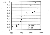
- Fig. 6 shows the amount of change in the cell gap of the liquid crystal when the amount of liquid crystal to be sealed is changed.
- the vertical axis represents the amount of compression obtained by subtracting the cell gap when the liquid crystal is sealed from the height of the spacer in an unloaded state.
- the horizontal axis represents the ratio of the amount of liquid crystal sealed to the design cell volume.
- the design cell volume referred to here is the product of the area of the region in which the liquid crystal is sealed (the region surrounded by the seal) and the height of the spacer in a no-load state.
- the measurement result in the display area of the liquid crystal panel according to the present embodiment (the present invention) and the measurement result in the display area of the conventional liquid crystal panel are shown.
- the cell gap in the display region does not change greatly even if the amount of liquid crystal to be sealed changes.
- the cell gap of the display region is also greatly changed according to the change of the amount of liquid crystal to be sealed.
- the non-display area can be deformed because the non-display area has a lower arrangement density of spacers than the display area. Therefore, even if the amount of liquid crystal to be sealed changes, the non-display area is deformed, so that the cell gap of the display area can be kept substantially constant.
- a liquid crystal cell in which the cell gap of the display region was maintained uniformly and stably without being affected by the amount of liquid crystal supplied could be produced.
- the liquid crystal display element according to the present invention can be applied to a liquid crystal display device such as a television receiver, a mobile phone, or a personal computer that displays an image with liquid crystal.
Landscapes
- Physics & Mathematics (AREA)
- Nonlinear Science (AREA)
- Mathematical Physics (AREA)
- Chemical & Material Sciences (AREA)
- Crystallography & Structural Chemistry (AREA)
- General Physics & Mathematics (AREA)
- Optics & Photonics (AREA)
- Liquid Crystal (AREA)
Abstract
液晶パネル(9)は、前面基板(1a)および背面基板(1b)と、両基板間に設けられた液晶層(3)とを備えている。前面基板(1a)と背面基板(1b)との接着にはシール(4)を利用している。上記1対の基板のいずれかと液晶層(3)とが接する領域が、表示領域(6)と、非表示領域(5)とに分割されている。表示領域(6)は、非表示領域(5)と比較して、単位面積あたりに配置されているスペーサ(2)の数が多い。換言すれば、表示領域(6)と非表示領域(5)とでスペーサ(2)の配置密度が異なり、非表示領域(5)と比較して表示領域(6)の配置密度は高い。これによって、表示領域(6)では、外部から圧力がかかっても大きな変形ができないため、非表示領域(5)がその圧力を受けて変形することになる。
Description
本発明は、液晶表示素子、およびその製造方法、ならびに当該液晶表示素子を備えた液晶表示装置に関し、より詳しくは、液晶表示素子を構成する1対の基板のうち、少なくとも一方が可撓性を有する液晶表示素子、およびその製造方法、ならびに当該液晶表示素子を備えた液晶表示装置に関する。
近年では、従来主流であったブラウン管を使用した表示装置から、薄型のフラットパネルディスプレイ(FPD)の表示装置が広く利用されるようになっている。FPDには、表示素子として液晶、発光ダイオード(LED)または、有機エレクトロルミネッセンス(有機EL)等を利用したものがある。中でも液晶を利用した表示装置は、薄型、軽量、および低消費電力という利点から、その研究開発が盛んに行われている。
一般的に、液晶表示装置は、バックライトと液晶表示素子とから構成されており、バックライトとしての面光源装置と、液晶表示素子としての液晶パネルとを有している。液晶パネルは、薄膜トランジスタ(TFT)、画素電極、および配向膜等を備える背面基板と、カラーフィルタ、対向電極、および配向膜等を備える前面基板との間に液晶を封入して構成されている。前面基板と背面基板との接着には枠状のシールを利用しており、当該シールには、基板同士を貼り合わせる接着剤としての役割と、基板間に注入される液晶が基板外部に漏れ出さないように封入するための封止剤としての役割とを有している。
最近では、液晶表示装置の製造効率を向上させるために、ロールツウロール(Roll to Roll)法による液晶表示装置の製造研究が進んでいる。このロールツウロール法では、上記シールを前面基板上に形成する工程から、背面基板と前面基板とを貼り合わせてシールを硬化する工程までを連続して行う。そのため、液晶の供給方法としては、液晶滴下工法(ODF法)が採用されている。当該ODF法では、前面基板上にシールを枠状に塗布した後、ディスペンサを用いて枠内に液晶を一定量ずつ滴下して液晶層を形成する。
液晶を供給する際には、適当な液晶量を供給しなければ、液晶セルのギャップが変化してしまい、液晶パネルの所定の性能を得ることができない。これは、液晶セルギャップが一定でないと、液晶パネルの光学特性も一定でなくなり、表示ムラ等が生じてしまうためである。このため、ODF法を用いて形成する液晶パネルでは、形成する液晶層の容積から滴下する液晶量を厳密に決定している。このように、両基板間のギャップを均一かつ安定に作製することは、高品位な表示を行う上で重要な要素となる。
ところで、従来では背面基板および前面基板としてガラス基板を主に用いていたが、軽量化あるいはフレキシブル化を目的としてポリイミドフィルム等のプラスチック基板を使用する試みがなされている。このようなフレキシブル基板を用いた液晶表示装置においても、液晶セルギャップを均一かつ安定に維持する対応が必要となる。しかしながら、ガラス基板と比較して当該フレキシブル基板は剛性を持たないため、撓み、またはうねり等により、セルギャップがばらついてしまう。このため、液晶パネルのセルギャップをより効果的に均一かつ安定に維持するための工夫が特許文献1および2では提案されている。
特許文献1には、液晶表示素子の製造方法として、液晶を注入した一対の基板を基板面に対して垂直な方向に加圧した状態で液晶注入口を封止する方法が開示されている。具体的には、シールが塗布された一対の基板を重ね合わせて、基板面に対して垂直な方向に均一に加圧する。基板を加圧し続けた状態でシールを硬化させ、液晶を液晶注入口から注入し、当該液晶注入口を封止する。これによれば、液晶注入口を封止する際、基板間に注入された過剰な液晶が液晶注入口から排出されて、液晶注入時に生じた基板間のギャップの膨張が矯正され、ギャップが均一化される。それと共に、その状態で液晶注入口が封止されるので、均一化されたギャップが以後も安定に保持される。
一方、特許文献2には、コラムスペーサが液晶セルに設けられている液晶表示素子が開示されている。具体的には、一対の基板のうち、一方の基板には、他方の基板に向かって突出しているコラムスペーサを形成されている。これによれば、コラムスペーサは、基板と接する部分の面積が広いので、両基板間を比較的に強く接着される。また、コラムスペーサは形成位置を自由に調節することができるので、両基板を全体にかけて均一に結合させることができる。これによって、液晶パネルのセルギャップが安定的に維持され、特に液晶パネルが撓む場合にもセルギャップが安定的に維持される。
以上で示した特許文献1および2に開示されている技術は、フレキシブル基板を採用した液晶表示装置に適用するのは困難である。
具体的には、上記した特許文献1に開示されている液晶表示素子の製造方法では、製造過程のハンドリング等を考慮すると、剛性がないフレキシブル基板に適用し難い。したがって、本文献に開示されている製造方法を用いて、セルギャップが均一化されたフレキシブル基板を有する液晶表示素子の製造の実現は難しい。また、本文献では、液晶層の形成方法として従来の真空注入法を想定しており、その製造工程が煩雑であるため、より生産性が高い製造方法が望まれる。
また、上記した特許文献2に開示されている液晶表示素子のように、柱状スペーサを介して背面基板と前面基板とを接着してしまうと、液晶パネルにフレキシブル基板を使用した場合には、液晶パネルが変形した際の応力が基板間の接着部にダメージを与えてしまう可能性がある。
そこで、本発明は上記課題に鑑みてなされたものであり、その目的は、フレキシブル基板を用いても液晶のセルギャップを均一かつ安定に維持することができる液晶表示素子、およびその製造方法、ならびに当該液晶表示素子を備えた液晶表示装置を提供することにある。
本発明に係る液晶表示素子は、上記課題を解決するために、少なくとも一方が可撓性を有する1対の基板間に設けられた液晶層と、当該液晶層を上記1対の基板間に封入し、かつ上記1対の基板間を接着するためのシールとを備えた液晶表示素子であって、上記液晶層内に配置され、上記1対の基板に接する複数のスペーサを備え、上記1対の基板のいずれかと上記液晶層とが接する領域が、表示領域と、当該表示領域を取り囲む非表示領域とに分割され、上記非表示領域の単位面積あたりに配置されている上記スペーサの数と比較して、上記表示領域の単位面積あたりに配置されている上記スペーサの数が多いことを特徴としている。
上記の構成によれば、表示領域は、非表示領域と比較して、単位面積あたりにスペーサが配置されている数が多い。換言すれば、表示領域と非表示領域とでスペーサの配置密度が異なり、非表示領域と比較して表示領域の配置密度は高い。これによって、表示領域では、外部から圧力がかかっても大きな変形ができないため、非表示領域がその圧力を受けて変形することになる。その結果、外部から圧力がかかっても非表示領域が変形することによって、表示領域のセルギャップをほぼ均一に維持することが可能である。このことから、本発明に係る液晶表示素子にフレキシブル基板を用いても表示領域における均一なセルギャップを維持することができる。
また、本発明の液晶表示素子に過剰な液晶を封入しても、表示領域における余剰な液晶は非表示領域に分配されるので、表示領域のセルギャップはほぼ均一に保たれる。逆に、本発明の液晶表示素子に必要よりも少ない液晶を封入した場合でも、非表示領域が変形することによって当該非表示領域における液晶量が少なくなり、表示領域のセルギャップをほぼ均一に維持することができる。このように、非表示領域はバッファとしての機能を有しており、分配される液晶量に合わせて変形し、液晶表示素子に封入される液晶量に依らず表示領域のセルギャップを均一かつ安定に維持することが可能である。
また、本発明に係る液晶表示装置は、上記課題を解決するために、上記したいずれかの液晶表示素子と、バックライトとを備えていることを特徴としている。
上記の構成によれば、液晶表示素子のセルギャップに不均衡が生じず、良好な表示品位を有する液晶表示装置を提供することができる。
また、本発明に係る液晶表示素子の製造方法においては、上記課題を解決するために、第1基板および第2基板の間に設けられた液晶層と、当該液晶層を上記第1基板および上記第2基板の間に封入し、かつ上記第1基板および上記第2基板の間を接着するためのシールとを備えた液晶表示素子の製造方法であって、上記第1基板上の表示領域と、当該表示領域を取り囲む非表示領域とに複数のスペーサを形成するスペーサ形成工程と、上記第1基板において上記複数のスペーサを形成した側の面に、上記複数のスペーサを取り囲むように上記シールを形成するシール形成工程と、上記シールに囲まれた領域内に上記液晶層を形成する液晶層形成工程と、上記第1基板上の上記複数のスペーサを上記第2基板に接着させ、かつ上記液晶層を形成した上記第1基板と、上記第2基板とを上記シールを介して接着する接着工程とを備え、上記スペーサ形成工程において、上記非表示領域の単位面積あたりに配置する上記スペーサの数と比較して、上記表示領域の単位面積あたりに配置する上記スペーサの数を多くすることを特徴としている。
上記の方法によれば、表示領域におけるセルギャップを均一かつ安定に維持することができる液晶表示素子を提供することができる。
本発明の他の目的、特徴、および優れた点は、以下に示す記載によって十分分かるであろう。また、本発明の利点は、添付図面を参照した次の説明で明白になるであろう。
本発明に係る液晶表示素子は、表示領域では、外部から圧力がかかっても大きな変形ができないため、非表示領域がその圧力を受けて変形することになる。その結果、非表示領域はバッファとして機能し、液晶表示素子に封入される液晶量に依らず表示領域のセルギャップを均一かつ安定に維持することが可能である。
以下では、本発明に係る液晶表示素子の好適な実施の形態について、図面を参照して詳細に説明する。
(液晶表示素子の構成)
一般的に、液晶表示装置(LCD)は、バックライトと液晶表示素子とから構成されており、バックライトとして面光源装置を有し、液晶表示素子として液晶パネルを有している。本実施形態に係る液晶パネルについて、図1を参照して説明する。図1中の(a)は、液晶パネル9の上面を示す図である。図1中の(b)は、図1中の(a)に示した領域7におけるA-A’断面を示す図である。図1中の(c)は、図1中の(a)に示した領域8におけるA-A’断面を示す図である。
一般的に、液晶表示装置(LCD)は、バックライトと液晶表示素子とから構成されており、バックライトとして面光源装置を有し、液晶表示素子として液晶パネルを有している。本実施形態に係る液晶パネルについて、図1を参照して説明する。図1中の(a)は、液晶パネル9の上面を示す図である。図1中の(b)は、図1中の(a)に示した領域7におけるA-A’断面を示す図である。図1中の(c)は、図1中の(a)に示した領域8におけるA-A’断面を示す図である。
図1中の(a)に示すように、液晶パネル9は、1対の基板(前面基板1aおよび背面基板1b)(第1基板,第2基板)と、両基板間に設けられた液晶層3とを備えている。前面基板1aと背面基板1bとの接着には枠状のシール4を利用しており、当該シール4には、基板同士を貼り合わせる接着剤としての役割と、基板間に注入される液晶が基板外部に漏れ出さないように封入するための封止剤としての役割とを有している。
さらに、液晶パネル9の前面基板1aまたは背面基板1bにおいて、液晶層3が接する領域(シール4に囲まれる領域)は、非表示領域5および表示領域6に分割されている。図1中の(b)に示すように、非表示領域5には、複数のスペーサ2が間隔を空けて形成されている。同様に、図1中の(c)に示すように、表示領域6にも、複数のスペーサ2が間隔を空けて形成されている。この際、非表示領域5に形成されている複数のスペーサ2は、表示領域6に形成されている複数のスペーサ2と比較して、隣り合うスペーサ2の間隔を大きくして形成されている。すなわち、非表示領域5と比較して、表示領域6の単位面積あたりに配置されているスペーサ2の数は多い。
スペーサ2は、フォトリソグラフィ法等によって形成される柱状のスペーサ、またはインクジェット法等によって散布される球状のスペーサ等である。柱状のスペーサ2を用いる場合は、その形状には特に限定はなく、円柱状のものであっても、角柱状のものであっても良い。当該スペーサ2は、配置位置を制御できる方法によって形成されるものであり、前面基板1aと背面基板1bとの間隔(すなわち、液晶のセルギャップ10)を一定に保つ役割がある。詳しくは後述する。
前面基板1aおよび背面基板1bにおいて、互いに対向する表面(以下、内表面という)には、酸化インジウム錫(ITO)膜等の透明電極(図示せず)がそれぞれ形成されている。前記前面基板1aおよび前記背面基板1bのうち、少なくとも一方が実質的に透明であれば良く、ガラス基板、セラミックス基板、またはプラスチック基板等を使用することができる。プラスチック基板としては、セルロース、トリアセチルセルロース、またはジアセチルセルロース等のセルロース誘導体、ポリシクロオレフィン誘導体、ポリエチレンテレフタレート、またはポリエチレンナフタレート等のポリエステル、ポリプロピレン、またはポリエチレン等のポリオレフィン、ポリカーボネート、ポリビニルアルコール、ポリ塩化ビニル、ポリ塩化ビニリデン、ポリアミド、ポリイミド、ポリイミドアミド、ポリスチレン、ポリアクリレート、ポリメチルメタクリレート、ポリエーテルサルホン、ポリアリレート、さらにガラス繊維-エポキシ樹脂、ガラス繊維-アクリル樹脂等の無機化合物と有機化合物との複合材料等を用いることができる。なお、本実施形態では、前面基板1aおよび背面基板1bのうち、少なくとも一方が可撓性を有していれば、その材質には特に限定はない。例えば、前面基板1aおよび背面基板1bの双方がガラス基板から構成されていても、少なくとも一方のガラス基板が可撓性を有していれば、本実施形態に含まれる。
液晶パネル9の駆動方式としては、例えば、単純マトリクス駆動方式、またはアクティブマトリクス駆動方式等が採用できる。液晶パネル9が採用する駆動方式に応じて、前面基板1aと背面基板1bとの内表面には、導電配線、スイッチング素子、および絶縁膜等が適宜形成される。また、両基板と液晶層3との界面には、配向処理された配向膜が必要に応じて形成される。
なお、液晶パネル9を液晶表示装置に用いるにあたっては、上記構成に加えて前面基板1aの内表面にはカラーフィルタを設け、前面基板1aおよび背面基板1bの少なくともいずれか一方の外表面(内表面とは反対側の面)には偏光板等を設ける。また、上述したように、液晶パネル9には、当該液晶パネル9を照明するバックライトとしての面光源装置、または反射板等が取り付けられる。これらの構成については、従来の液晶表示装置と同様であるため、ここでは言及しない。
(スペーサ2とセルギャップ10との関係)
上述したように、本実施形態に係る液晶パネル9には、液晶のセルギャップ10を一定に保つために複数のスペーサ2を液晶層3内に形成している。この際、本実施形態では、場所によって複数のスペーサ2の配置密度(単位面積あたりに配置されているスペーサ2の数)が異なることを特徴としている。より具体的には、非表示領域5におけるスペーサ2の配置密度が相対的に低くなるようにし、表示領域6におけるスペーサ2の配置密度が相対的に高くなるようにしている。これによって、表示領域6のセルギャップ10は、供給される液晶量の影響を受けにくくなり、適正なセルギャップ10を安定に維持することができる。その詳しいメカニズムを説明するために、図2に示すような液晶パネル29を例に挙げる。図2は、前面基板21aまたは背面基板21bにおいて、シール24に囲まれる領域を8つの領域に分けた液晶パネル29の上面を示す図である。
上述したように、本実施形態に係る液晶パネル9には、液晶のセルギャップ10を一定に保つために複数のスペーサ2を液晶層3内に形成している。この際、本実施形態では、場所によって複数のスペーサ2の配置密度(単位面積あたりに配置されているスペーサ2の数)が異なることを特徴としている。より具体的には、非表示領域5におけるスペーサ2の配置密度が相対的に低くなるようにし、表示領域6におけるスペーサ2の配置密度が相対的に高くなるようにしている。これによって、表示領域6のセルギャップ10は、供給される液晶量の影響を受けにくくなり、適正なセルギャップ10を安定に維持することができる。その詳しいメカニズムを説明するために、図2に示すような液晶パネル29を例に挙げる。図2は、前面基板21aまたは背面基板21bにおいて、シール24に囲まれる領域を8つの領域に分けた液晶パネル29の上面を示す図である。

図2に示すように、液晶パネル29では、シール24に囲まれる領域を8つの領域(A~H)に分け、領域ごとにスペーサ2の配置密度およびサイズが異なるように当該スペーサ2を形成している。領域ごとに形成したスペーサ2の配置密度およびサイズを表1に示す。ここでいうスペーサ2のサイズとは、スペーサ2が前面基板21aまたは背面基板21bに接触する面積である。なお、表1中の領域Iとは、領域Bに形成したスペーサ2と同じ種類のスペーサ2を用いた従来の液晶パネル内の一領域である。表1に示すように、領域A~Dでは、小さいサイズ(225μm2/個)のスペーサ2を用い、その配置密度を異ならせている(1.56~100個/mm2)。一方、領域E~Hでは、大きいサイズ(900μm2/個)のスペーサ2を用い、その配置密度を異ならせている(1.56~100個/mm2)。
液晶パネル29の構成は、本実施形態に係る液晶パネル9に準じており、液晶パネル9と同様の各部材を備えているものである。具体的には、液晶パネル29では、前面基板21aおよび背面基板21bは、ガラス繊維-アクリル樹脂の複合材料により構成されているフィルム基板であり、その厚さは100μmである。両基板の内表面には、それぞれ透明電極、柱状のスペーサ2、および配向膜が順次形成されている。また、前面基板21aと背面基板21bとの間には、ツイストネマティック(TN)型液晶をシール24で封入した液晶層が形成されている。
液晶パネル29において、封入する液晶量を変化させた際の、液晶のセルギャップ10の変動量を図3および図4に示す。具体的には、液晶滴下工法(ODF法)によって液晶を封入した際のセルギャップ10を、無荷重状態でのスペーサ2の高さから差し引いた変動量を縦軸に示す。また、横軸には、設計セル容積に対する、封入した液晶量の割合を示す。ここでいう設計セル容積とは、液晶を封入する領域(シール24に囲まれる領域)の面積と、無荷重状態でのスペーサ2の高さとの積である。なお、領域I以外の領域における測定は、すべて真空気泡を含んでいない液晶セルで行っている。
まず、領域Bおよび領域Iの測定結果を図3に示す。上述したように、領域Iでは、領域Bに形成したスペーサ2と同じ配置密度およびサイズのスペーサ2を液晶セルに形成した構成になっている。この場合、図3に示すように、封入する液晶量ごとにセルギャップ10は変化している。最小二乗法でのフィッティングの結果、液晶量が設定セル容積に対して5%変化すると、セルギャップ10には0.22μmの変動が生じている。このことから、一定のセルギャップ10を保つためには、供給する液晶量と、設計セル容積とを正確に制御することが重要なポイントであることが分かる。しかしながら、フレキシブル基板は剛性を持たないため、撓み、またはうねり等により、セルギャップ10がばらついてしまう。その結果、液晶パネルの表示品位の低下をもたらしてしまう。
一方、領域Bでは、図3に示すように、封入する液晶量ごとのセルギャップ10の変動量は小さい。最小二乗法でのフィッティングの結果、セルギャップ10の変動量は領域Iの1/10にまで低減されており、供給される液晶量に依らずほぼ一定の値となっている。したがって、供給する液晶量が変化しても、セルギャップ10をほぼ一定に保つことが可能となる。以下では、その理由を詳しく説明する。
領域A~Hの測定結果を図4に示す。図4に示すように、スペーサ2の配置密度が1.56個/mm2または6.25個/mm2と低い領域C,D,G,Hでは、液晶量の変化に対するセルギャップ10の変動量が大きくなっている。逆に、スペーサ2の配置密度が100個/mm2または25個/mm2と高い領域A,B,E,Fでは、スペーサ2のサイズに依らずほぼ一定の値となっている。したがって、設計セル容積に対して少量の液晶を封入した場合でも、セルギャップ10はほぼ変動しない。すなわち、液晶パネル29に供給された液晶は、まずは領域A,B,E,Fに優先的に分配される。その後、供給される液晶量が増加するにつれ、領域A,B,E,Fにおいて余剰となる液晶が領域C,D,G,Hに流れ込む。このように、スペーサ2の配置密度が低い領域C,D,G,Hは、領域A,B,E,Fのセルギャップ10を均一かつ安定に維持するためのバッファとしての機能を有している。
スペーサ2の配置密度差に起因する液晶の分配について、図5を参照して詳しく説明する。図5中の(a)は、液晶パネル9にかかる大気圧の方向を簡易的に示す図である。図5中の(b)は、設計セル容積と同量の液晶を封入した場合における、非表示領域5の断面を示す図である。図5中の(c)は、設計セル容積と同量の液晶を封入した場合における、表示領域6の断面を示す図である。図5中の(d)は、設計セル容積よりも少ない量の液晶を封入した場合における、非表示領域5の断面を示す図である。図5中の(e)は、設計セル容積よりも少ない量の液晶を封入した場合における、表示領域6の断面を示す図である。
上述したように、本実施形態では、非表示領域5におけるスペーサ2の配置密度が相対的に低くなるようにし、表示領域6におけるスペーサ2の配置密度が相対的に高くなるようにしている。
図5中の(a)に示すように、前面基板1aと背面基板1bとを貼り合わせた後の液晶パネル9には、設計セル容積と、封入した液晶の体積との差の容積に相当する圧力が大気より(矢印の方向から)均一にかかっている。ここで、図5中の(b)および(c)に示すように、設計セル容積と同量の液晶を封入した場合には、設計セル容積と封入した液晶の体積とが同じであるため、大気からの圧力はかからない。これは、スペーサ2の配置密度の高低には関係ない。そのため、図5中の(b)に示した非表示領域5のセルギャップ10と、図5中の(c)に示した表示領域6のセルギャップ10とは同等である。したがって、以上の場合では、非表示領域5および表示領域6においても、均一かつ安定なセルギャップ10を維持することができる。
なお、図5中の(d)および(e)に示すように、設計セル容積よりも少ない量の液晶を封入した場合には、液晶パネル9には設計セル容積と封入された液晶の体積との差の容積に相当する圧力が大気よりかかる。ここで、図5中の(d)に示した非表示領域5、および図5中の(e)に示した表示領域6のいずれにも同等の圧力がかかる。しかしながら、非表示領域5ではスペーサ2の配置密度が低いため、スペーサ2の配置密度が高い表示領域6と比較して、大気圧によるスペーサ2の圧縮量が大きくなる。その結果、図5中の(d)に示した非表示領域5のセルギャップ10は、図5中の(e)に示した表示領域6のセルギャップ10よりも小さくなる。
さらに、非表示領域5でのスペーサ2の配置密度が小さいことから、スペーサ2の設置間隔は、表示領域6でのスペーサ2の設置間隔よりも大きい。そのため、非表示領域5全体が撓む度合いも大きくなる。その結果、非表示領域5における単位面積あたりの液晶量は、表示領域6における単位面積あたりの液晶量よりも小さくなる。
以上により、スペーサ2の配置密度が高い領域(表示領域6)では、外部から圧力がかかっても大きな変形ができないため、スペーサ2の配置密度が低い領域(非表示領域5)がその圧力を受けて変形することになる。その結果、スペーサ2の配置密度が高い領域は、そのセルギャップ10が変わらず維持されることになる。このように、液晶セル内に、スペーサ2の配置密度が高い領域と、スペーサ2の配置密度が低い領域とを形成することによって、スペーサ2の配置密度が低い領域はバッファとして機能する。ここで、スペーサ2の配置密度が低い領域をバッファとしてより効果的に機能させるためには、フレキシブル基板を利用することが好ましい。これによれば、フレキシブル基板の可撓性を利用して、液晶量の変化に対して容積を容易に変化させることができる。
なお、本実施形態では、フレキシブル基板(前面基板1aおよび背面基板1b)が厚さ100μmの例を示したが、特にこれに限定されるわけではない。例えば、100μmよりも薄くすることによって、フレキシブル基板のフレキシブル性が増すので、より効果的である。

図4に示した各領域(A~H)での封入液晶量が最大であるときのセルギャップ10と、封入液晶量が最小であるときのセルギャップ10との差を最大圧縮量として表2に示す。表2に示すように、領域A~Dに着目すると、スペーサ2の配置密度が低くなるにつれて最大圧縮量が大きくなっているのが分かる。同様に領域E~Hについても、スペーサ2の配置密度が低くなるにつれて最大圧縮量が大きくなっている。この際、最も配置密度が小さい領域Dおよび領域Hのうち、最大圧縮量が最も大きかったのは領域Dである。領域Dの最大圧縮量は2.08μmであるため、セルギャップ10は約2μm変動可能ということである。したがって、領域Dは、それに相当する液晶量のバッファとなっている。
このことにより、スペーサ2の配置密度に差がある領域を同一平面上に複数設けることによって、スペーサ2の配置密度が低い領域は、スペーサ2の配置密度が高い領域に対するバッファとして機能する。これによって、封入する液晶量に依らず、スペーサ2の配置密度が高い領域のセルギャップ10を均一かつ安定に維持することが可能となる。
本実施形態では、表示領域6におけるスペーサ2の配置密度よりも低い配置密度でスペーサ2を非表示領域5に形成することによって、非表示領域5にバッファとしての機能を持たせることができる。具体的には、液晶パネル9に過剰な液晶を封入しても、表示領域6における余剰な液晶は非表示領域5に分配されるので、表示領域6のセルギャップ10をほぼ均一に保たれる。逆に、液晶パネル9に必要よりも少ない液晶を封入した場合でも、非表示領域5が変形することによって当該非表示領域5における液晶量が少なくなり、表示領域6のセルギャップ10はほぼ均一に維持することができる。このように、非表示領域5は分配される液晶量に合わせて変形し、液晶パネル9に封入される液晶量に依らず表示領域6のセルギャップ10を均一かつ安定に維持することが可能である。
したがって、本実施形態では、フレキシブル基板を用いた場合に、液晶パネル9に外部から圧力がかかっても、撓み、またはうねり等によるセルギャップ10の不均衡は生じない。逆に、当該フレキシブル基板のフレキシブル性を利用して非表示領域5がバッファとして柔軟に対応することができる。すなわち、本実施形態では、フレキシブル基板を用いた場合でも表示領域6におけるセルギャップ10を均一かつ安定に維持することができる。
以上では、表示領域6と比較して非表示領域5のスペーサ2の配置密度が低いことが好ましいと述べたが、より詳細には、非表示領域5のスペーサ2の配置密度は、表示領域6のスペーサ2の配置密度の1/4以下であることが好ましい。これは、1/4倍を超えると、非表示領域5および表示領域6におけるスペーサ2の配置密度差を利用したバッファ効果が低下する虞があるためである。
また、非表示領域5のスペーサ2の高さは、表示領域6のスペーサ2の高さよりも高いことが好ましい。これによれば、非表示領域5のスペーサ2の高さを高くすることによって、当該非表示領域5のスペーサ2の高さが表示領域6のスペーサ2と同じである場合と比較して、非表示領域5における変形量をより大きくすることができる。その結果、非表示領域5において、分配される液晶量をより多くすることができ、より効果的にバッファとしての機能を発揮することができる。また、非表示領域5のスペーサ2の高さを高くすれば、非表示領域5の面積を小さくしても十分なバッファとしての機能が得られるので、液晶パネル9の額縁を狭めることの有効な手段となる。
さらに、スペーサ2の高さを変える以外にも、柱状のスペーサ2であれば、スペーサ2のサイズを変更することによって、非表示領域5のバッファとしての機能をより高めることができる。例えば、表2に示したように、領域Cおよび領域Gにおいては、スペーサ2の配置密度は同じであるが、領域Gのスペーサ2の方が当該スペーサ2のサイズが大きい。そのため、領域Cのスペーサ2の方が圧縮されやすいことから、その最大圧縮量が領域Gと比較して大きい。領域Dおよび領域Hについても同様である。
このように、非表示領域5におけるスペーサ2が前面基板1aまたは背面基板1bと接触する面積を小さくすることによって、非表示領域5が変形しやすくなる。したがって、スペーサ2の配置密度に差をつけることによって、スペーサ2の配置密度が小さい領域の変形量を変えることができるが、スペーサ2のサイズに差をつけることによってその変形量を調整しても良い。
あるいは、フレキシブル基板(前面基板1aおよび背面基板1b)の厚さ、または弾性率等の機械特性を非表示領域5と表示領域6とで差をつけることによっても、上記と同様の効果を得ることができる。例えば、前面基板1aおよび背面基板1bの少なくとも一方は、表示領域6における基板の厚さを、非表示領域5における基板の厚さよりも厚くすると良い。これによれば、非表示領域5はより変形しやすくなり、バッファとしての機能を効果的に発揮することができる。
また、前面基板1aおよび背面基板1bの少なくとも一方は、表示領域6における基板の弾性率を、非表示領域5における基板の弾性率よりも大きくすると良い。これは、弾性率をヤング率Eとして想定すると、ε=σ/Eと表されためである。なお、εは歪みであり、σは圧縮応力である。表示領域6における歪量を小さくするためには、弾性率(ヤング率)を大きくすると良い。逆に、非表示領域5における歪量を大きくするためには、弾性率(ヤング率)を小さくすると良い。これによれば、非表示領域5はより歪みやすくなり、バッファとしての機能を効果的に発揮することができる。このように、非表示領域5と表示領域6とにおいて、外部からの圧力による容積変化に差が生じるような構成であれば、より効果的に表示領域6のセルギャップ10を均一かつ安定に維持することができる。
(液晶パネル9の製造方法)
続いて、本実施形態に係る液晶パネル9の製造方法について説明する。なお、上述したように、前面基板1aおよび背面基板1bは、例えば、アクティブマトリクス素子アレイ、カラーフィルタ、透明電極、または配向膜等の液晶表示素子として機能するための構成を有しているものとする。これらの部材の形成方法は、従来の液晶パネルの製造工程における同部材の形成方法と同様であるため、ここではその形成方法については言及しない。以下では、スペーサ形成工程、シール形成工程、液晶層形成工程、および接着工程の各工程について順に説明する。なお、本実施形態では、ロールツウロール法を適用するのが好ましい。これは、スペーサ形成工程から、接着工程までを一連の工程として行うため、液晶パネル9の製造効率を高めることができるためである。また、ロールツウロール法は、フレキシブル基板に好適に用いられるためでもある。
続いて、本実施形態に係る液晶パネル9の製造方法について説明する。なお、上述したように、前面基板1aおよび背面基板1bは、例えば、アクティブマトリクス素子アレイ、カラーフィルタ、透明電極、または配向膜等の液晶表示素子として機能するための構成を有しているものとする。これらの部材の形成方法は、従来の液晶パネルの製造工程における同部材の形成方法と同様であるため、ここではその形成方法については言及しない。以下では、スペーサ形成工程、シール形成工程、液晶層形成工程、および接着工程の各工程について順に説明する。なお、本実施形態では、ロールツウロール法を適用するのが好ましい。これは、スペーサ形成工程から、接着工程までを一連の工程として行うため、液晶パネル9の製造効率を高めることができるためである。また、ロールツウロール法は、フレキシブル基板に好適に用いられるためでもある。
まずスペーサ形成工程では、表示領域6と、当該表示領域6の外周部に位置する非表示領域5とにスペーサ2を形成する。スペーサ2の形成方法としては、フォトリソグラフィ法が挙げられる。この方法では、スペーサ2のパターンとして所望なパターンを予めフォトマスクに形成しておくことによって、非表示領域5および表示領域6の双方に同時にスペーサ2を形成することができる。本フォトリソグラフィ法によっては、柱状のスペーサ2が得られる。球状のスペーサ2を用いる場合には、インクジェット法が適用可能である。本インクジェット法によって、球状のスペーサ2を非表示領域5および表示領域6に塗り分ければ良い。この際、非表示領域5および表示領域6に形成するスペーサ2の配置密度およびサイズは、それぞれ適当なものを選択する。
なお、本工程の前工程となるが、カラーフィルタを形成する際に、非表示領域5のスペーサ2を形成する位置に、ブラックマトリクス、およびRGBの各色層を積層して形成しておくと良い。これによれば、新たな工程を導入することなく、非表示領域5に配置されるスペーサ2の高さを、表示領域6に配置されるスペーサ2の高さよりも高くすることができる。当該非表示領域5のスペーサ2の高さは、重ねる色層の数によって調整することが可能である。
次にシール形成工程では、液晶を封入する領域を規定するための枠状のシール4を形成する。シール4の形成方法としては、ディスペンサによる描画法またはスクリーン印刷法等が適用可能である。シール4は、前面基板1aまたは背面基板1bの内表面に形成する。以下では、前面基板1aにシール4を形成した場合を想定して説明する。
液晶層形成工程では、上記シール形成工程で形成したシール4に囲まれる領域に液晶を供給する。液晶の供給方法としては、液晶滴下工法(ODF法)または真空注入法が挙げられるが、本実施形態においては、ODF法を用いるのが好ましい。これは、ODF法がフレキシブル基板に適したロールツウロール法に対応しているためである。この際、供給する液晶量は、シール4に囲まれる領域の面積と、無荷重状態のスペーサ2の高さとの積である設計セル容積に合わせて決定する。なお、厳密には、供給する液晶量は、設計セル容積と液晶セル内に形成しているスペーサ2の容積とを考慮した上で決定する。そのため、設計セル容積およびスペーサ2の容積を厳密に求める必要があるので、供給すべき液晶量を正確に決定するのは難しい。しかし、本実施形態では、供給する液晶量が過剰な場合でも、必要よりも少ない場合でも、非表示領域5が変形することによって、表示領域6のセルギャップ10をほぼ一定に保つことができるため、問題ない。
最後に、接着工程では、前面基板1aと背面基板1bとを貼り合わせる。具体的には、基板を吸着する静電チャック等の機構を備えたステージに前面基板1aと背面基板1bとを吸着させ、前面基板1aの配向膜(内表面)と背面基板1bの配向膜(内表面)とが向き合い、前面基板1a上に形成したシール4と、背面基板1bとが接しない位置に配置する。そして、この状態で系内を減圧し、減圧終了後に前面基板1aと背面基板1bとの貼り合わせ位置を確認しながら両基板の位置を調整する(アライメント操作)。貼り合わせ位置の調整が終了すると、前面基板1a上のシール4と背面基板1bとが接する位置まで両基板を接近させる。この状態で系内に不活性ガスを充填し、徐々に圧力を上げて常圧に戻す。この際、大気圧によって前面基板1aと背面基板1bとが接着され、スペーサ2の高さに相当するセルギャップ10が形成される。この状態でシール4に紫外線を照射して硬化することによって、液晶パネル9が得られる。
このように形成された液晶パネル9では、非表示領域5および表示領域6に配置されたスペーサ2の配置密度が異なり、表示領域6に比べて非表示領域5のスペーサ2の配置密度は低くなっている。これによって、非表示領域5はバッファとしての機能を有しており、液晶パネル9に封入される液晶量に依らず表示領域6のセルギャップ10を均一かつ安定に維持することが可能である。
また、以上のようにロールツウロール法によって製造すれば、セルギャップ10が均一かつ安定な液晶パネル9を再現性高く製造することが可能となる。
本発明は、上述した実施形態に限定されるものではなく、請求項に示した範囲で種々の変更が可能である。すなわち、請求項に示した範囲で適宜変更した技術的手段を組み合わせて得られる実施形態についても本発明の技術的範囲に含まれる。
例えば、液晶表示素子として本実施形態に係る液晶パネル9を用いた液晶表示装置も、本発明に含まれることは言うまでもない。
〔実施形態の総括〕
以上のように、本発明に係る液晶表示素子においては、上記非表示領域に配置されている上記スペーサの高さと比較して、上記表示領域に配置されている上記スペーサの高さが低いことを特徴としている。
以上のように、本発明に係る液晶表示素子においては、上記非表示領域に配置されている上記スペーサの高さと比較して、上記表示領域に配置されている上記スペーサの高さが低いことを特徴としている。
上記の構成によれば、非表示領域のスペーサの高さを高くすることによって、当該非表示領域のスペーサの高さが表示領域のスペーサと同じである場合と比較して、非表示領域の変形の度合いをより大きくすることができる。その結果、非表示領域において、蓄えることができる液晶量が多くなるので、より効果的にバッファとしての機能を発揮することができる。
また、本発明に係る液晶表示素子においては、上記非表示領域に配置されている上記スペーサが上記1対の基板のいずれかと接する面積と比較して、上記表示領域に配置されている上記スペーサが上記1対の基板のいずれかと接する面積が大きいことを特徴としている。
上記の構成によれば、非表示領域におけるスペーサが両基板と接触する面積を小さくすることによって、非表示領域が変形しやすくなる。その結果、液晶セルにおける液晶量に依らず、非表示領域が変形することによって、表示領域のセルギャップをほぼ一定に保つことができる。
また、本発明に係る液晶表示素子においては、上記非表示領域の単位面積あたりに配置されている上記スペーサの数は、上記表示領域の単位面積あたりに配置されている上記スペーサの数の1/4以下であることを特徴としている。
上記の構成によれば、非表示領域および表示領域におけるスペーサの配置密度の差を利用した非表示領域のバッファとしての機能を十分に得ることができる。
また、本発明に係る液晶表示素子においては、上記スペーサは、柱状または球状であることを特徴としている。
上記の構成によれば、表示領域におけるセルギャップをほぼ一定に保ちつつ、非表示領域において圧縮することによって当該非表示領域を変形させることができる。
また、本発明に係る液晶表示素子においては、上記1対の基板の少なくとも一方は、上記表示領域における当該基板の厚さが、上記非表示領域における当該基板の厚さと比較して厚いことを特徴としている。
また、本発明に係る液晶表示素子においては、上記1対の基板の少なくとも一方は、上記表示領域における当該基板の弾性率が、上記非表示領域における当該基板の弾性率と比較して大きいことを特徴としている。
上記の構成によれば、非表示領域はより変形しやすくなるので、表示領域におけるセルギャップをより効果的に一定に保つことが可能となる。
発明の詳細な説明の項においてなされた具体的な実施形態または実施例は、あくまでも、本発明の技術内容を明らかにするものであって、そのような具体例にのみ限定して狭義に解釈されるべきものではなく、本発明の精神と次に記載する請求の範囲内で、いろいろと変更して実施することができるものである。
以下、実施例を挙げて本発明をさらに詳しく説明するが、本発明はその要旨を超えない限り、これら実施例に限定されるものではない。
上述の製造方法に従って、サイズ3.5型(QVGA)の液晶パネルを作製した。スペーサとしては、柱状のスペーサをフォトリソグラフィ法によって形成した。当該液晶パネルにおける表示領域のスペーサは、QVGAの1画素につき1個の配置密度で配置した。一方、非表示領域のスペーサは、表示領域におけるスペーサの配置密度の1/4程度の配置密度とした。なお、表示領域および非表示領域共に、スペーサが前面基板または背面基板に接する面積(スペーサのサイズ)は225μm2/個とした。非表示領域は、表示領域の外周に幅4.4mmで形成した。この際、形成した液晶セルの容積における、表示領域の容積に対する非表示領域の容積の比率は、およそ10%である。これは、それぞれの領域の面積と、それぞれの領域のスペーサの高さとに基づいて計算されたものである。
封入する液晶量を変化させた際の、液晶のセルギャップの変動量を図6に示す。具体的には、液晶を封入した際のセルギャップを、無荷重状態でのスペーサの高さから差し引いた圧縮量を縦軸に示す。また、横軸には、設計セル容積に対する、封入した液晶量の割合を示す。ここでいう設計セル容積とは、液晶を封入する領域(シールに囲まれる領域)の面積と、無荷重状態でのスペーサの高さとの積である。本図では、本実施例(本発明)に係る液晶パネルの表示領域における測定結果と、従来の液晶パネルの表示領域における測定結果とを示している。
図6に示すように、本実施例に係る液晶パネルにおいては、封入する液晶量が変化しても、表示領域のセルギャップが大きく変化しない。一方、従来の液晶パネルにおいては、封入する液晶量の変化に応じて、表示領域のセルギャップも大きく変化している。これは、本実施例に係る液晶パネルにおいては、非表示領域は表示領域と比較してスペーサの配置密度が低いため、非表示領域が変形可能となっている。そのため、封入される液晶量が変化しても、非表示領域が変形することによって、表示領域のセルギャップをほぼ一定に保つことができる。このように、本実施例では、供給する液晶量の影響を受けることがなく、表示領域のセルギャップが均一かつ安定に維持された液晶セルを作製することができた。
本発明に係る液晶表示素子は、液晶によって画像を表示するテレビジョン受像機、携帯電話、またはパーソナルコンピュータ等の液晶表示装置に適用できる。
1a,21a 前面基板
1b,21b 背面基板
2 スペーサ
3 液晶層
4,24 シール
5 非表示領域
6 表示領域
7,8 領域
9,29 液晶パネル
10 セルギャップ
1b,21b 背面基板
2 スペーサ
3 液晶層
4,24 シール
5 非表示領域
6 表示領域
7,8 領域
9,29 液晶パネル
10 セルギャップ
Claims (9)
- 少なくとも一方が可撓性を有する1対の基板間に設けられた液晶層と、当該液晶層を上記1対の基板間に封入し、かつ上記1対の基板間を接着するためのシールとを備えた液晶表示素子であって、
上記液晶層内に配置され、上記1対の基板に接する複数のスペーサを備え、
上記1対の基板のいずれかと上記液晶層とが接する領域が、表示領域と、当該表示領域を取り囲む非表示領域とに分割され、
上記非表示領域の単位面積あたりに配置されている上記スペーサの数と比較して、上記表示領域の単位面積あたりに配置されている上記スペーサの数が多いことを特徴とする液晶表示素子。 - 上記非表示領域に配置されている上記スペーサの高さと比較して、上記表示領域に配置されている上記スペーサの高さが低いことを特徴とする請求項1に記載の液晶表示素子。
- 上記非表示領域に配置されている上記スペーサが上記1対の基板のいずれかと接する面積と比較して、上記表示領域に配置されている上記スペーサが上記1対の基板のいずれかと接する面積が大きいことを特徴とする請求項1に記載の液晶表示素子。
- 上記非表示領域の単位面積あたりに配置されている上記スペーサの数は、上記表示領域の単位面積あたりに配置されている上記スペーサの数の1/4以下であることを特徴とする請求項1~3のいずれか1項に記載の液晶表示素子。
- 上記スペーサは、柱状または球状であることを特徴とする請求項1~4のいずれか1項に記載の液晶表示素子。
- 上記1対の基板の少なくとも一方は、上記表示領域における当該基板の厚さが、上記非表示領域における当該基板の厚さと比較して厚いことを特徴とする請求項1~5のいずれか1項に記載の液晶表示素子。
- 上記1対の基板の少なくとも一方は、上記表示領域における当該基板の弾性率が、上記非表示領域における当該基板の弾性率と比較して大きいことを特徴とする請求項1~5のいずれか1項に記載の液晶表示素子。
- 請求項1~7のいずれか1項に記載の液晶表示素子と、バックライトとを備えていることを特徴とする液晶表示装置。
- 第1基板および第2基板の間に設けられた液晶層と、当該液晶層を上記第1基板および上記第2基板の間に封入し、かつ上記第1基板および上記第2基板の間を接着するためのシールとを備えた液晶表示素子の製造方法であって、
上記第1基板上の表示領域と、当該表示領域を取り囲む非表示領域とに複数のスペーサを形成するスペーサ形成工程と、
上記第1基板において上記複数のスペーサを形成した面に、上記複数のスペーサを取り囲むように上記シールを形成する、または上記第2基板において上記複数のスペーサに対向する面に、当該複数のスペーサに相対する領域を取り囲むように上記シールを形成するシール形成工程と、
上記シールに囲まれた領域内に上記液晶層を形成する液晶層形成工程と、
上記第1基板上の上記複数のスペーサを上記第2基板に接着させ、かつ上記第1基板と上記第2基板とを上記シールを介して接着する接着工程とを備え、
上記スペーサ形成工程において、上記非表示領域の単位面積あたりに配置する上記スペーサの数と比較して、上記表示領域の単位面積あたりに配置する上記スペーサの数を多くすることを特徴とする液晶表示素子の製造方法。
Priority Applications (1)
| Application Number | Priority Date | Filing Date | Title |
|---|---|---|---|
| US13/636,297 US20130016308A1 (en) | 2010-03-31 | 2011-01-21 | Liquid crystal display element, method for manufacturing same, and liquid crystal display device comprising the liquid crystal display element |
Applications Claiming Priority (2)
| Application Number | Priority Date | Filing Date | Title |
|---|---|---|---|
| JP2010-083745 | 2010-03-31 | ||
| JP2010083745A JP2013122471A (ja) | 2010-03-31 | 2010-03-31 | 液晶表示素子、およびその製造方法、ならびに当該液晶表示素子を備えた液晶表示装置 |
Publications (1)
| Publication Number | Publication Date |
|---|---|
| WO2011122076A1 true WO2011122076A1 (ja) | 2011-10-06 |
Family
ID=44711829
Family Applications (1)
| Application Number | Title | Priority Date | Filing Date |
|---|---|---|---|
| PCT/JP2011/051121 Ceased WO2011122076A1 (ja) | 2010-03-31 | 2011-01-21 | 液晶表示素子、およびその製造方法、ならびに当該液晶表示素子を備えた液晶表示装置 |
Country Status (3)
| Country | Link |
|---|---|
| US (1) | US20130016308A1 (ja) |
| JP (1) | JP2013122471A (ja) |
| WO (1) | WO2011122076A1 (ja) |
Cited By (1)
| Publication number | Priority date | Publication date | Assignee | Title |
|---|---|---|---|---|
| WO2017063426A1 (zh) * | 2015-10-16 | 2017-04-20 | 京东方科技集团股份有限公司 | 液晶显示器及其制造方法 |
Families Citing this family (9)
| Publication number | Priority date | Publication date | Assignee | Title |
|---|---|---|---|---|
| US10270058B2 (en) * | 2012-03-30 | 2019-04-23 | Nec Lighting, Ltd. | Organic electroluminescent illumination panel, manufacturing method thereof, and organic electroluminescent illumination device |
| KR102242439B1 (ko) * | 2014-09-30 | 2021-04-20 | 삼성디스플레이 주식회사 | 곡면형 액정 표시 장치 |
| CN104570498B (zh) * | 2014-11-24 | 2017-10-13 | 深圳市华星光电技术有限公司 | 可挠曲液晶面板及其制作方法 |
| KR102516055B1 (ko) | 2016-07-05 | 2023-03-31 | 삼성디스플레이 주식회사 | 플렉서블 디스플레이 장치 |
| JP7083603B2 (ja) | 2017-07-27 | 2022-06-13 | 株式会社ジャパンディスプレイ | 表示装置 |
| JP2019198908A (ja) * | 2018-05-15 | 2019-11-21 | 株式会社ディスコ | 合成樹脂板加工方法 |
| US10901268B2 (en) * | 2018-10-18 | 2021-01-26 | Liqxtal Technology Inc. | Liquid crystal phase modulation device having spacer in liquid crystal layer and method for fabricating the same |
| WO2020261315A1 (ja) * | 2019-06-24 | 2020-12-30 | 三菱電機株式会社 | 湾曲型の液晶表示装置 |
| CN118946847A (zh) * | 2022-03-30 | 2024-11-12 | 株式会社Lg化学 | 液晶单元和光学装置 |
Citations (6)
| Publication number | Priority date | Publication date | Assignee | Title |
|---|---|---|---|---|
| JP2004126197A (ja) * | 2002-10-02 | 2004-04-22 | Toshiba Corp | 液晶表示装置 |
| WO2006077838A1 (ja) * | 2005-01-20 | 2006-07-27 | Sharp Kabushiki Kaisha | 液晶表示素子 |
| WO2007083412A1 (ja) * | 2006-01-17 | 2007-07-26 | Sharp Kabushiki Kaisha | 液晶表示装置 |
| WO2009054292A1 (ja) * | 2007-10-22 | 2009-04-30 | Citizen Holdings Co., Ltd. | 液晶表示素子 |
| JP2009098426A (ja) * | 2007-10-17 | 2009-05-07 | Sharp Corp | 液晶表示パネル及びその製造方法 |
| JP2010048887A (ja) * | 2008-08-19 | 2010-03-04 | Hitachi Displays Ltd | 表示装置 |
Family Cites Families (5)
| Publication number | Priority date | Publication date | Assignee | Title |
|---|---|---|---|---|
| JP4081643B2 (ja) * | 2001-08-01 | 2008-04-30 | 株式会社日立製作所 | 液晶表示装置 |
| US7286204B2 (en) * | 2003-03-28 | 2007-10-23 | Samsung Electronics Co., Ltd. | Spacers for display devices |
| TWI271574B (en) * | 2004-04-30 | 2007-01-21 | Innolux Display Corp | Liquid crystal display panel |
| KR20060081210A (ko) * | 2005-01-07 | 2006-07-12 | 삼성전자주식회사 | 액정표시장치 |
| KR20130021160A (ko) * | 2011-08-22 | 2013-03-05 | 삼성디스플레이 주식회사 | 표시 장치 및 표시 장치 제조 방법 |
-
2010
- 2010-03-31 JP JP2010083745A patent/JP2013122471A/ja active Pending
-
2011
- 2011-01-21 WO PCT/JP2011/051121 patent/WO2011122076A1/ja not_active Ceased
- 2011-01-21 US US13/636,297 patent/US20130016308A1/en not_active Abandoned
Patent Citations (6)
| Publication number | Priority date | Publication date | Assignee | Title |
|---|---|---|---|---|
| JP2004126197A (ja) * | 2002-10-02 | 2004-04-22 | Toshiba Corp | 液晶表示装置 |
| WO2006077838A1 (ja) * | 2005-01-20 | 2006-07-27 | Sharp Kabushiki Kaisha | 液晶表示素子 |
| WO2007083412A1 (ja) * | 2006-01-17 | 2007-07-26 | Sharp Kabushiki Kaisha | 液晶表示装置 |
| JP2009098426A (ja) * | 2007-10-17 | 2009-05-07 | Sharp Corp | 液晶表示パネル及びその製造方法 |
| WO2009054292A1 (ja) * | 2007-10-22 | 2009-04-30 | Citizen Holdings Co., Ltd. | 液晶表示素子 |
| JP2010048887A (ja) * | 2008-08-19 | 2010-03-04 | Hitachi Displays Ltd | 表示装置 |
Cited By (2)
| Publication number | Priority date | Publication date | Assignee | Title |
|---|---|---|---|---|
| WO2017063426A1 (zh) * | 2015-10-16 | 2017-04-20 | 京东方科技集团股份有限公司 | 液晶显示器及其制造方法 |
| US10162223B2 (en) | 2015-10-16 | 2018-12-25 | Boe Technology Group Co., Ltd. | Liquid crystal display and manufacturing method thereof |
Also Published As
| Publication number | Publication date |
|---|---|
| JP2013122471A (ja) | 2013-06-20 |
| US20130016308A1 (en) | 2013-01-17 |
Similar Documents
| Publication | Publication Date | Title |
|---|---|---|
| JP2013122471A (ja) | 液晶表示素子、およびその製造方法、ならびに当該液晶表示素子を備えた液晶表示装置 | |
| CN101216635B (zh) | 液晶显示装置、光电装置及其制造方法 | |
| KR102603601B1 (ko) | 디스플레이 장치 및 그의 제조 방법 | |
| US8253883B2 (en) | Display panel and display device | |
| CN101639619B (zh) | 立体图像显示设备及其制造方法 | |
| EP2977673B1 (en) | Liquid crystal display and manufacturing method thereof | |
| US10062740B2 (en) | Display device with a buffer layer filled with bubbles and packaging method | |
| US20100085507A1 (en) | Display apparatus and method of fabricating the same | |
| US9835898B2 (en) | Display unit | |
| JP5288729B2 (ja) | 液晶表示装置 | |
| US20070019134A1 (en) | Polarizing film assembly, method of manufacturing the same and display device having the same | |
| CN102177538A (zh) | 显示装置及其制造方法 | |
| US9915759B2 (en) | Polarizing plate, liquid crystal display device having the same and method of fabricating the polarizing plate | |
| US20120154344A1 (en) | Electric paper display apparatus | |
| KR20080110090A (ko) | 굴절률 감쇠 필름, 이를 구비한 편광 부재, 및 이를 구비한표시 장치 | |
| CN1844979A (zh) | 液晶显示器件及其制造方法 | |
| US7521272B2 (en) | Display device producing method and display device producing device | |
| US11448913B2 (en) | Display device and fabrication method thereof | |
| KR20120066177A (ko) | 액정표시장치 | |
| US20060215105A1 (en) | Liquid crystal display device with photo spacers | |
| US10295729B2 (en) | Liquid crystal display device | |
| US20110032178A1 (en) | Display Device | |
| CN103760719A (zh) | 一种显示基板及显示装置 | |
| US20120285608A1 (en) | Method for producing liquid crystal panel | |
| US20130021572A1 (en) | Liquid crystal display device element, method for manufacturing same, and liquid crystal display device |
Legal Events
| Date | Code | Title | Description |
|---|---|---|---|
| 121 | Ep: the epo has been informed by wipo that ep was designated in this application |
Ref document number: 11762317 Country of ref document: EP Kind code of ref document: A1 |
|
| WWE | Wipo information: entry into national phase |
Ref document number: 13636297 Country of ref document: US |
|
| NENP | Non-entry into the national phase |
Ref country code: DE |
|
| 122 | Ep: pct application non-entry in european phase |
Ref document number: 11762317 Country of ref document: EP Kind code of ref document: A1 |
|
| NENP | Non-entry into the national phase |
Ref country code: JP |