WO2011121778A1 - 薄膜多結晶シリコン、その製造方法および薄膜多結晶シリコンを製造するプラズマ装置 - Google Patents
薄膜多結晶シリコン、その製造方法および薄膜多結晶シリコンを製造するプラズマ装置 Download PDFInfo
- Publication number
- WO2011121778A1 WO2011121778A1 PCT/JP2010/055946 JP2010055946W WO2011121778A1 WO 2011121778 A1 WO2011121778 A1 WO 2011121778A1 JP 2010055946 W JP2010055946 W JP 2010055946W WO 2011121778 A1 WO2011121778 A1 WO 2011121778A1
- Authority
- WO
- WIPO (PCT)
- Prior art keywords
- pressure
- reaction vessel
- polycrystalline silicon
- crystal grains
- thin film
- Prior art date
- Legal status (The legal status is an assumption and is not a legal conclusion. Google has not performed a legal analysis and makes no representation as to the accuracy of the status listed.)
- Ceased
Links
Images







Classifications
-
- C—CHEMISTRY; METALLURGY
- C23—COATING METALLIC MATERIAL; COATING MATERIAL WITH METALLIC MATERIAL; CHEMICAL SURFACE TREATMENT; DIFFUSION TREATMENT OF METALLIC MATERIAL; COATING BY VACUUM EVAPORATION, BY SPUTTERING, BY ION IMPLANTATION OR BY CHEMICAL VAPOUR DEPOSITION, IN GENERAL; INHIBITING CORROSION OF METALLIC MATERIAL OR INCRUSTATION IN GENERAL
- C23C—COATING METALLIC MATERIAL; COATING MATERIAL WITH METALLIC MATERIAL; SURFACE TREATMENT OF METALLIC MATERIAL BY DIFFUSION INTO THE SURFACE, BY CHEMICAL CONVERSION OR SUBSTITUTION; COATING BY VACUUM EVAPORATION, BY SPUTTERING, BY ION IMPLANTATION OR BY CHEMICAL VAPOUR DEPOSITION, IN GENERAL
- C23C16/00—Chemical coating by decomposition of gaseous compounds, without leaving reaction products of surface material in the coating, i.e. chemical vapour deposition [CVD] processes
- C23C16/22—Chemical coating by decomposition of gaseous compounds, without leaving reaction products of surface material in the coating, i.e. chemical vapour deposition [CVD] processes characterised by the deposition of inorganic material, other than metallic material
- C23C16/24—Deposition of silicon only
-
- C—CHEMISTRY; METALLURGY
- C23—COATING METALLIC MATERIAL; COATING MATERIAL WITH METALLIC MATERIAL; CHEMICAL SURFACE TREATMENT; DIFFUSION TREATMENT OF METALLIC MATERIAL; COATING BY VACUUM EVAPORATION, BY SPUTTERING, BY ION IMPLANTATION OR BY CHEMICAL VAPOUR DEPOSITION, IN GENERAL; INHIBITING CORROSION OF METALLIC MATERIAL OR INCRUSTATION IN GENERAL
- C23C—COATING METALLIC MATERIAL; COATING MATERIAL WITH METALLIC MATERIAL; SURFACE TREATMENT OF METALLIC MATERIAL BY DIFFUSION INTO THE SURFACE, BY CHEMICAL CONVERSION OR SUBSTITUTION; COATING BY VACUUM EVAPORATION, BY SPUTTERING, BY ION IMPLANTATION OR BY CHEMICAL VAPOUR DEPOSITION, IN GENERAL
- C23C16/00—Chemical coating by decomposition of gaseous compounds, without leaving reaction products of surface material in the coating, i.e. chemical vapour deposition [CVD] processes
- C23C16/44—Chemical coating by decomposition of gaseous compounds, without leaving reaction products of surface material in the coating, i.e. chemical vapour deposition [CVD] processes characterised by the method of coating
- C23C16/50—Chemical coating by decomposition of gaseous compounds, without leaving reaction products of surface material in the coating, i.e. chemical vapour deposition [CVD] processes characterised by the method of coating using electric discharges
- C23C16/505—Chemical coating by decomposition of gaseous compounds, without leaving reaction products of surface material in the coating, i.e. chemical vapour deposition [CVD] processes characterised by the method of coating using electric discharges using radio frequency discharges
- C23C16/509—Chemical coating by decomposition of gaseous compounds, without leaving reaction products of surface material in the coating, i.e. chemical vapour deposition [CVD] processes characterised by the method of coating using electric discharges using radio frequency discharges using internal electrodes
-
- H—ELECTRICITY
- H01—ELECTRIC ELEMENTS
- H01J—ELECTRIC DISCHARGE TUBES OR DISCHARGE LAMPS
- H01J37/00—Discharge tubes with provision for introducing objects or material to be exposed to the discharge, e.g. for the purpose of examination or processing thereof
- H01J37/32—Gas-filled discharge tubes
- H01J37/32009—Arrangements for generation of plasma specially adapted for examination or treatment of objects, e.g. plasma sources
- H01J37/32082—Radio frequency generated discharge
-
- H—ELECTRICITY
- H01—ELECTRIC ELEMENTS
- H01J—ELECTRIC DISCHARGE TUBES OR DISCHARGE LAMPS
- H01J37/00—Discharge tubes with provision for introducing objects or material to be exposed to the discharge, e.g. for the purpose of examination or processing thereof
- H01J37/32—Gas-filled discharge tubes
- H01J37/32431—Constructional details of the reactor
- H01J37/32532—Electrodes
- H01J37/32541—Shape
Definitions
- the present invention relates to a thin film polycrystalline silicon, a manufacturing method thereof, and a plasma apparatus for manufacturing the thin film polycrystalline silicon.
- Patent Document 1 a polycrystalline silicon thin film formed on a substrate is known (Patent Document 1).
- This polycrystalline silicon thin film has a structure of substrate / microcrystalline silicon / polycrystalline silicon.
- Polycrystalline silicon is composed of crystal grains having a columnar structure connected in the normal direction of the substrate.
- an object of the present invention is to provide a thin film polycrystalline silicon capable of producing a device on either the surface side or the substrate side.
- Another object of the present invention is to provide a method for producing thin film polycrystalline silicon capable of producing a device on either the surface side or the substrate side.
- Another object of the present invention is to provide a plasma apparatus for producing a thin film polycrystalline silicon capable of producing a device on either the surface side or the substrate side.
- the thin film polycrystalline silicon includes an underlayer and n (n is a positive integer) silicon crystal grains.
- the underlayer is made of any one of an insulator, a metal, and a semiconductor.
- the n silicon crystal grains are formed on the base layer and arranged in the normal direction of the base layer. Of the n silicon crystal grains, the silicon crystal grain closest to the base layer is in contact with the base layer. In each of the n silicon crystal grains, the length in the normal direction is longer than the length in the in-plane direction of the underlayer.
- each of the n silicon crystal grains has a substantially columnar shape.
- the n silicon crystal grains are composed of one silicon crystal grain.
- One silicon crystal grain has a substantially inverted conical shape in the normal direction.
- the n silicon crystal grains are composed of two or more silicon crystal grains.
- the surface orientation of two or more silicon crystal grains changes from the (220) plane to the (111) plane as the distance from the base layer increases.
- a manufacturing method includes an insulator, a metal, and a plasma device using a plasma device that generates a plasma by supplying high-frequency power to an electrode made of a substantially U-shaped conductor disposed in a reaction vessel.
- a manufacturing method for manufacturing thin film polycrystalline silicon on an underlayer made of any of semiconductors the first step of supplying a material gas containing silicon atoms into a reaction vessel, and (220) in X-ray diffraction analysis
- the thin film polycrystalline silicon is composed of n (n is a positive integer) silicon crystal grains arranged in the normal direction of the underlayer.
- n is a positive integer
- the pressure in the reaction vessel is the critical pressure.
- the intensity ratio is adjusted to a pressure that sets the desired intensity ratio.
- the second step includes a first sub-step of adjusting the pressure in the reaction vessel to a first pressure that sets the intensity ratio to the first desired intensity ratio in a pressure range lower than the critical pressure;
- the thin film polycrystalline silicon is composed of n (n is a positive integer) silicon crystal grains arranged in the normal direction of the underlayer, and the shape of the silicon crystal grains is substantially cylindrical to substantially in the normal direction.
- the pressure in the reaction vessel when the pressure in the reaction vessel when changing to an inverted conical shape is the critical pressure, the pressure in the reaction vessel is set to a desired strength ratio in the pressure range higher than the critical pressure in the second step. It is adjusted to the pressure to do.
- the plasma apparatus is a plasma apparatus for producing thin film polycrystalline silicon on a base layer made of any one of an insulator, a metal, and a semiconductor, comprising: a reaction vessel; And a second electrode, a pressure regulator, and a high-frequency power source.
- the first electrode is disposed in the reaction vessel and is made of a substantially U-shaped conductor having a first length.
- the second electrode is disposed in the reaction vessel and is made of a substantially U-shaped conductor having a second length shorter than the first length.
- the pressure adjuster adjusts the pressure in the reaction vessel to a pressure that sets the intensity ratio, which is the ratio of the peak intensity of the (111) plane to the peak intensity of the (220) plane in X-ray diffraction analysis, to a desired intensity ratio.
- the high frequency power supply supplies high frequency power to the first and second electrodes.
- the first electrode is placed in a region other than a region where plasma for producing thin-film polycrystalline silicon is generated.
- the thin film polycrystalline silicon is composed of n (n is a positive integer) silicon crystal grains arranged in the normal direction of the underlayer, and the shape of the silicon crystal grains is substantially cylindrical to substantially in the normal direction.
- the pressure regulator adjusts the pressure in the reaction vessel to a pressure that sets the strength ratio to a desired strength ratio in a pressure range lower than the critical pressure. Adjust.
- the pressure regulator is responsive to a first pressure that sets the intensity ratio to a first desired intensity ratio in a pressure range lower than the critical pressure during a first period from the start of the production of thin film polycrystalline silicon.
- the pressure in the container is adjusted, and after the end of the first period, the intensity ratio is set to the second desired intensity ratio in a pressure range lower than the critical pressure, and the second pressure is lower than the first pressure. Adjust the pressure in the reaction vessel.
- the thin film polycrystalline silicon is composed of n (n is a positive integer) silicon crystal grains arranged in the normal direction of the underlayer, and the shape of the silicon crystal grains is substantially cylindrical to substantially in the normal direction.
- the pressure regulator is set to a pressure that sets the intensity ratio to a desired intensity ratio in a pressure range higher than the critical pressure. Adjust.
- the plasma apparatus further includes first and second flat plate members.
- the first flat plate member is connected to one end of the second electrode outside the reaction vessel.
- the second flat plate member is disposed opposite to the first flat plate member, connected to the other end of the second electrode, and one end on the same side as the one end of the first flat plate member is grounded. Is done.
- the thin film polycrystalline silicon according to the embodiment of the present invention includes n silicon crystal grains.
- the n silicon crystal grains are formed on the base layer and arranged in the normal direction of the base layer. Of the n silicon crystal grains, the silicon crystal grain closest to the base layer is in contact with the base layer.
- a device can be fabricated on either the surface side or the base layer side of the n silicon crystal grains arranged in the normal direction of the base layer.
- FIG.1 and FIG.2 It is a perspective view of the antenna and flat plate member which are shown in FIG. It is a figure which shows the relationship between the peak intensity of a X-ray diffraction analysis, and the pressure at the time of reaction. It is a figure which shows the relationship between the peak intensity of a X-ray diffraction analysis, and high frequency electric power.
- FIG. 1 is a cross-sectional view of thin-film polycrystalline silicon according to an embodiment of the present invention.
- thin film polycrystalline silicon 10 according to an embodiment of the present invention includes a substrate 1 and polycrystalline silicon 2.
- the substrate 1 is made of any one of a metal, an insulator, and a semiconductor.
- substrate 1 it is stainless steel, for example.
- the insulator constituting the substrate 1 include glass and quartz.
- the semiconductor constituting the substrate 1 are silicon (Si) and germanium (Ge).
- the polycrystalline silicon 2 is formed on the substrate 1 in contact with the substrate 1.
- the polycrystalline silicon 2 has a structure in which a plurality of columnar crystals 20 are arranged in the in-plane direction of the substrate 1.
- the columnar crystal 20 is composed of, for example, three silicon crystal grains 21 to 23.
- the silicon crystal grains 21 to 23 are arranged in the normal direction of the substrate 1.
- Each of the silicon crystal grains 21 to 23 has a length d1 in the normal direction of the substrate 1 longer than a length d2 in the in-plane direction of the substrate 1. That is, each of the silicon crystal grains 21 to 23 has a columnar shape that is crystal-grown in the normal direction of the substrate 1.
- the length d1 is, for example, 30 to 300 nm
- the length d2 is, for example, 5 to 30 nm.
- the silicon crystal grains 21 are formed on the substrate 1 in contact with the substrate 1.
- the silicon crystal grains 22 are formed on the silicon crystal grains 21.
- the silicon crystal grains 23 are formed on the silicon crystal grains 22.
- the columnar crystal 20 is composed of three silicon crystal grains 21-23.
- the columnar crystal 20 is composed of a number of silicon crystal grains determined by the thickness of the polycrystalline silicon 2. That is, the columnar crystal 20 is made up of a larger number of silicon crystal grains when the thickness of the polycrystalline silicon 2 is increased, and from a smaller number of silicon crystal grains when the thickness of the polycrystalline silicon 2 is reduced. Become.
- the columnar crystal 20 is composed of two or more silicon crystal grains 21 to 23
- the columnar crystal 20 is formed of three silicon crystal grains 21 to 23. Actually, however, the columnar crystal 20 is visually observed as one silicon crystal. It appears to be formed from grains. As a result of analysis by TEM (Transmission Electron Microscope), it is understood that the columnar crystal 20 is composed of a plurality of silicon crystal grains 21 to 23 arranged in the normal direction of the substrate 1.
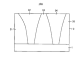
- FIG. 2 is a cross-sectional view of another thin film polycrystalline silicon according to the embodiment of the present invention.
- the thin film polycrystalline silicon according to the embodiment of the present invention may be thin film polycrystalline silicon 10A shown in FIG.
- thin film polycrystalline silicon 10A is the same as thin film polycrystalline silicon 10 except that polycrystalline silicon 2 of thin film polycrystalline silicon 10 shown in FIG. It is.
- the polycrystalline silicon 3 is formed on the substrate 1 in contact with the substrate 1.
- the polycrystalline silicon 3 is composed of silicon crystal grains 31-35. Each of the silicon crystal grains 31 to 35 is formed on the substrate 1 in contact with the substrate 1. Each of the silicon crystal grains 31 to 35 is connected in the normal direction of the substrate 1.
- the silicon crystal grains 31 to 35 are generally longer in the normal direction of the substrate 1 than in the in-plane direction of the substrate 1.
- the lengths of the silicon crystal grains 31, 33, 35 in the in-plane direction of the substrate 1 become longer in the normal direction of the substrate 1 as it approaches the substrate 1.
- the silicon crystal grains 32 and 34 have a longer length in the in-plane direction of the substrate 1 as they move away from the substrate 1 in the normal direction of the substrate 1.
- the shape of the silicon crystal grains 32 and 34 is referred to as an “inverted cone”.
- the thin film polycrystalline silicon 10 and 10A includes the polycrystalline silicon 2 and 3 formed in contact with the substrate 1 and the substrate 1 made of any one of an insulator, a metal, and a semiconductor.
- a device can be fabricated on either the surface side of 2, 3 or the substrate 1 side.
- the thin film polycrystalline silicon 10 is suitable for, for example, a light emitting element, and the thin film polycrystalline silicon 10A is suitable for, for example, a solar cell and a TFT (Thin Film Transistor).
- TFT Thin Film Transistor
- the silicon crystal grains 31 to 35 are connected in the normal direction of the substrate 1, and therefore, the carrier can easily travel in the normal direction of the substrate 1.
- FIG. 3 is a cross-sectional view showing a configuration of a plasma apparatus for manufacturing the thin film polycrystalline silicon 10, 10A shown in FIGS.
- plasma apparatus 100 includes antennas 101 to 105, reaction vessel 100, substrate holder 120, introduction terminals 121, 123, 125, 127, and 129, and heater 130.
- the reaction vessel 110 has a substantially rectangular parallelepiped outer shape and is hollow inside.
- the reaction vessel 110 includes a main body 111, a lid 112, and an O-ring 113.
- Each of the main body 111 and the lid 112 is made of stainless steel and connected to the ground potential GND.
- the main body 111 has a gas supply port 114 and an exhaust port 115.
- the lid 112 is disposed in contact with the O-ring 113.
- the O-ring 113 is inserted into a groove provided around the main body 111 and contacts the main body 111 and the lid 112. As a result, the O-ring 113 keeps the inside of the reaction vessel 110 airtight.
- Each of the antennas 101 to 105 is made of, for example, copper (Cu).
- the antennas 101 to 105 are disposed inside the reaction container 110.
- the antennas 101 to 104 are arranged at a predetermined interval along the lid 112 of the reaction vessel 110.
- the antennas 101 to 104 are connected at one end side to the flat plate member 131 through the introduction terminals 121, 123, 125, and 127, respectively.
- the other ends of the antennas 101 to 104 are connected to the ground potential GND through another introduction terminal (not shown).
- One end of the antenna 105 is connected to the flat plate member 131 through the introduction terminal 129. Further, the other end side of the antenna 105 is connected to the ground potential GND through another introduction terminal (not shown).
- Each of the antennas 101 to 104 has a length of 30 to 40 cm, for example, and the antenna 105 has a length of 50 to 60 cm, for example. That is, each of the antennas 101 to 104 is shorter than the antenna 105.
- the antennas 101 to 104 are installed to face the plasma region 180 where plasma for producing the thin film polycrystalline silicon 10 or 10A is generated.
- the antenna 105 is installed in a region other than the plasma region 180.
- the introduction terminals 121, 123, 125, 127, and 129 are fixed to the lid 112 of the reaction vessel 110.
- the flat plate member 131 is made of Cu, for example.
- the flat plate member 131 is disposed substantially parallel to the lid 112 of the reaction vessel 110 outside the reaction vessel 110.
- the flat plate member 131 has one surface connected to one end of the antennas 101 to 105.
- the flat plate member 131 is connected to the matching unit 160 at one end in the direction DR1 parallel to the lid 112.
- the substrate holder 120 is fixed to the bottom surface 111A of the main body 111 of the reaction vessel 110.
- the heater 130 is disposed inside the substrate holder 120.
- the gas supply device 140 is connected to the gas inlet 114 of the reaction vessel 110.
- the exhaust device 150 is connected to the exhaust port 115 of the reaction vessel 110.
- Matching device 160 is connected between one end of flat plate member 131 in the arrangement direction of antennas 101 to 105 and high-frequency power supply 170.
- the high frequency power source 170 is connected between the matching unit 160 and the ground potential GND.
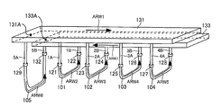
- FIG. 4 is a perspective view of the antennas 101 to 105 and the flat plate member 131 shown in FIG. Referring to FIG. 4, plasma apparatus 100 further includes introduction terminals 122, 124, 1216, 128 and 132.
- the introduction terminals 122, 124, 126, 128, 132 are fixed to the lid 112 of the reaction vessel 110 in the same manner as the introduction terminals 121, 123, 125, 127, 129.
- the flat plate member 131 has, for example, a width of 1 cm, a thickness of 1 cm, and a length of 1 m.
- Each of the antennas 101 to 105 has a substantially U shape.
- the antennas 101 to 105 are arranged so that five planes including the antennas 101 to 105 bent into a substantially U shape are substantially parallel to each other.
- the straight portions 1A, 2A, 3A, 4A, and 5A are connected to the flat plate member 131 through the introduction terminals 121, 123, 125, 127, and 129, respectively.
- the straight portions 1B, 2B, 3B, 4B, and 5B are connected to the ground potential GND through the introduction terminals 122, 124, 126, 128, and 132, respectively.
- the antennas 101 to 105 have a pair of introduction terminals 121 and 122, a pair of introduction terminals 123, 124, and 1, respectively.
- the pair of introduction terminals 125 and 126, the pair of introduction terminals 127 and 128, and the pair of introduction terminals 129 and 132 are fixed to the lid 112 of the reaction vessel 110.
- antennas 101 to 105 when high frequency power is supplied from high frequency power supply 170 to antennas 101-105 via matching unit 160 and flat plate member 131, antennas 101 to 105 have high frequencies in the direction from flat plate member 131 toward ground potential GND. A current is passed, and plasma is generated in the reaction vessel 110 by inductive coupling.
- the antenna 105 when high-frequency power is supplied from the high-frequency power supply 170, the antenna 105 first generates plasma, and then the antennas 101 to 104 generate plasma.
- the antenna 105 Since the antenna 105 is longer than the antennas 101 to 104, it is easier to generate plasma than the antennas 101 to 104. Therefore, the antenna 105 serves as a trigger when generating plasma.
- the substrate holder 120 holds the substrate 1.
- the introduction terminals 121 to 129 and 132 fix the antennas 101 to 105 to the lid 112 of the reaction vessel 10 and shield the gap between the antennas 101 to 105 and the lid 112.
- the heater 130 heats the substrate 1 installed on the substrate holder 120 to a predetermined temperature.
- the gas supply device 140 includes a material gas for forming a semiconductor thin film such as silane (SiH 4 ) gas and disilane (Si 2 H 6 ), a dilution gas such as hydrogen (H 2 ) gas and nitrogen (N 2 ) gas, Etching gas such as argon (Ar) gas is supplied into the reaction vessel 110 through the gas supply port 114.
- a material gas for forming a semiconductor thin film such as silane (SiH 4 ) gas and disilane (Si 2 H 6 )
- a dilution gas such as hydrogen (H 2 ) gas and nitrogen (N 2 ) gas
- Etching gas such as argon (Ar) gas is supplied into the reaction vessel 110 through the gas supply port 114.
- the exhaust device 150 is composed of, for example, a turbo molecular pump and a rotary pump, and evacuates the reaction vessel 110 through the exhaust port 115 and adjusts the pressure in the reaction vessel 110 to a desired pressure.
- the matching unit 160 supplies the high frequency power supplied from the high frequency power source 170 to the flat plate member 131 while suppressing reflection.
- the high frequency power supply 170 supplies, for example, high frequency power of 13.56 MHz to the matching unit 160.
- the high frequency power supply 170 supplies high frequency power to the flat plate member 131 via the matching unit 160
- the high frequency current flows from the connection point 131A between the flat plate member 131 and the matching unit 160 in the direction of the arrow ARW1, and the straight lines of the antennas 101 to 105 are connected. It flows into portions 1A, 2A, 3A, 4A, and 5A.
- the high-frequency current flows through the antenna 101 in the direction of the arrow ARW2 and flows to the ground potential GND.
- the high-frequency current flows through the antenna 102 in the direction of the arrow ARW3 and flows to the ground potential GND.
- the high frequency current flows through the antenna 103 in the direction of the arrow ARW4 and flows to the ground potential GND.
- the high frequency current flows through the antenna 104 in the direction of the arrow ARW5 and then flows to the ground potential GND.
- the high-frequency current flows through the antenna 105 in the direction of the arrow ARW6 and then flows to the ground potential GND.
- the present invention is characterized by including the antenna 105 that functions as a trigger when generating plasma.
- the plasma apparatus 100 manufactures thin film polycrystalline silicon 10 and 10A using SiH 4 gas.
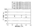
- FIG. 5 is a diagram showing the relationship between the peak intensity of the X-ray diffraction analysis and the pressure during the reaction.
- the vertical axis represents the peak intensity of X-ray diffraction analysis
- the horizontal axis represents the pressure during the reaction.
- the black square indicates the peak intensity of the (111) plane when # 1737 / Ti / W is used as the substrate 1, and the black triangle indicates (111) when quartz / Ti / W is used as the substrate 1. Indicates the peak intensity of the surface.
- the white square indicates the peak intensity of the (220) plane when # 1737 / Ti / W is used as the substrate 1, and the white triangle indicates (220) when quartz / Ti / W is used as the substrate 1. Indicates the peak intensity of the surface.
- the reaction conditions are that the high-frequency power is 1.7 kW, the flow rate of SiH 4 gas is 2.5 sccm, the flow rate of H 2 gas is 30 sccm, the substrate temperature is 420 ° C., and the reaction pressure is 0.8. 8 Pa, 1.3 Pa, 1.8 Pa, and 2.4 Pa.
- the film thickness of the deposited polycrystalline silicon is 2 ⁇ m.
- the peak intensity of the (111) plane is almost constant with respect to the reaction pressure. This tendency is independent of the type of the substrate 1.
- FIG. 6 is a diagram showing the relationship between the peak intensity of the X-ray diffraction analysis and the high-frequency power.
- the vertical axis represents the peak intensity of the X-ray diffraction analysis
- the horizontal axis represents the high frequency power.
- black triangles, black squares, and black circles indicate the peak intensity of the (111) plane when # 1737 / Ti / W is used as the substrate 1.
- white triangles, white squares, and white circles indicate the peak intensity of the (220) plane when # 1737 / Ti / W is used as the substrate 1.
- reaction conditions are such that the high frequency power is 1.7 kW, 2.0 kW, and 2.2 kW, the flow rate of SiH 4 gas is 2.5 sccm, the flow rate of H 2 gas is 30 sccm, and the substrate temperature is 420 ° C.
- the reaction pressure is 1.8 Pa.
- the film thickness of the deposited polycrystalline silicon is 2 ⁇ m.
- the peak intensity of the (111) plane slightly decreases as the high frequency power increases.
- the peak intensity of the (220) plane hardly changes even when the high frequency power is increased.
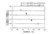
- FIG. 7 is a graph showing the relationship between the ratio of the peak intensity of the (111) plane to the peak intensity of the (220) plane in X-ray diffraction analysis and the pressure during the reaction.
- the vertical axis represents the ratio of the peak intensity of the (111) plane to the peak intensity of the (220) plane
- the horizontal axis represents the pressure during the reaction.
- the black rhombus indicates the ratio of the peak intensity of the (111) plane to the peak intensity of the (220) plane when # 1737 / Ti / W is used as the substrate 1, and the black square indicates quartz / Ti as the substrate 1.
- the ratio of the peak intensity of the (111) plane to the peak intensity of the (220) plane when / W is used is shown.
- the reaction conditions are that the high-frequency power is 1.7 kW, the flow rate of SiH 4 gas is 2.5 sccm, the flow rate of H 2 gas is 30 sccm, the substrate temperature is 420 ° C., and the reaction pressure is 0.8. 8 Pa, 1.3 Pa, 1.8 Pa, and 2.4 Pa.
- the film thickness of the deposited polycrystalline silicon is 2 ⁇ m.
- the ratio of the peak intensity of (111) plane to the peak intensity of (220) plane decreases as the reaction pressure increases, and increases as the reaction pressure decreases.
- the ratio of the peak intensity of the (111) plane to the peak intensity of the (220) plane changes substantially linearly with respect to the change in reaction pressure.
- the reaction pressure of 1.8 Pa is a critical pressure at which the silicon crystal grains change from a columnar shape to an inverted conical shape.
- the film thickness is determined based on the relationship between the reaction pressure and the ratio of the peak intensity of the (111) plane to the peak intensity of the (220) plane shown in FIG.
- the pressure in the reaction vessel 110 is determined.
- FIG. 8 is a diagram showing the relationship between the stress of the film and the pressure during the reaction.
- the vertical axis represents the stress of the film
- the horizontal axis represents the pressure during the reaction.
- the reaction conditions are such that the high-frequency power is 1.7 kW, the flow rate of SiH 4 gas is 2.5 sccm, the flow rate of H 2 gas is 30 sccm, the substrate temperature is 420 ° C., and the reaction pressure is 0.8. 8 Pa, 1.3 Pa, 1.8 Pa, and 2.4 Pa.
- the film thickness of the deposited polycrystalline silicon is 2 ⁇ m.
- the stress of the film is a compressive stress, and the compressive stress decreases as the reaction pressure increases and increases as the reaction pressure decreases.
- the thin film polycrystalline silicon 10 has a larger compressive stress than the thin film polycrystalline silicon 10A.
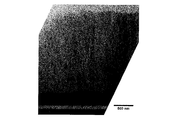
- FIG. 9 to 11 are cross-sectional TEM images of thin film polycrystalline silicon.
- the thin film polycrystalline silicon shown in FIG. 9 has a high frequency power of 1.7 kW, a flow rate of SiH 4 gas is 2.5 sccm, a flow rate of H 2 gas is 30 sccm, a substrate temperature is 420 ° C. It was produced under reaction conditions with a pressure of 1.8 Pa.
- the film thickness is 2 ⁇ m.
- the 10 has a high-frequency power of 1.7 kW, a flow rate of SiH 4 gas of 2.5 sccm, a flow rate of H 2 gas of 30 sccm, and a substrate temperature of 420 ° C.
- the reaction pressure was 1.3 Pa.
- the film thickness is 1.6 ⁇ m.
- the thin film polycrystalline silicon shown in FIG. 11 has a high frequency power of 1.7 kW, a flow rate of SiH 4 gas is 2.5 sccm, a flow rate of H 2 gas is 30 sccm, and the substrate temperature is 420 ° C.
- the reaction pressure was 1.3 Pa / 1.0 Pa. That is, the thin film polycrystalline silicon shown in FIG. 11 was produced by switching the reaction pressure from 1.3 Pa to 1.0 Pa. In this case, the reaction pressure was switched from 1.3 Pa to 1.0 Pa when a 1.6 ⁇ m thin film polycrystalline silicon was formed at a reaction pressure of 1.3 Pa.
- the total film thickness is 2 ⁇ m.
- the polycrystalline silicon is formed from the initial stage of film formation and is in contact with the substrate.
- columnar polycrystalline silicon is formed in the region where the reaction pressure is lower than 1.8 Pa.
- the surface of the polycrystalline silicon is flat.
- the thin film polycrystalline silicon manufactured using the plasma apparatus 100 changes its film structure, plane orientation and stress depending on the reaction pressure.
- FIG. 12 is a process diagram showing a method of manufacturing the thin-film polycrystalline silicon 10, 10A shown in FIGS.
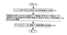
- the gas supply device 140 supplies a material containing silicon atoms into the reaction vessel 110 (step S1).
- the exhaust device 150 sets the intensity ratio, which is the ratio of the peak intensity of the (111) plane to the peak intensity of the (220) plane in the X-ray diffraction analysis, to a desired intensity ratio.
- the pressure in the reaction vessel 110 is adjusted to the pressure (step S2).
- the high frequency power supply 170 supplies high frequency power to the antennas 101 to 105 via the matching unit 160 (step S3).
- the antenna 105 serves as a trigger, and plasma is generated in the reaction vessel 110, the thin film polycrystalline silicon 10 or the thin film polycrystalline silicon 10A is manufactured, and the series of operations ends.
- step S2 the reaction pressure is not fixed to one pressure, but may be changed.
- the first sub-process to be adjusted, and the exhaust device 15 sets the intensity ratio to the second desired intensity ratio in a pressure range lower than the critical pressure, and reacts to the second pressure lower than the first pressure.
- a second sub-process for adjusting the pressure in the container 110 is a second sub-process for adjusting the pressure in the container 110.
- the pressure in the reaction vessel 110 is adjusted to a second pressure lower than the first pressure.
- polycrystalline silicon can be manufactured from the initial stage of film formation. Further, since the ratio of the peak intensity of the (111) plane to the peak intensity of the (220) plane varies greatly depending on the reaction pressure, thin film polycrystalline silicon having various intensity ratios can be manufactured.
- FIG. 13 is a cross-sectional view showing the configuration of another plasma apparatus for manufacturing the thin film polycrystalline silicon shown in FIGS.
- the plasma apparatus for producing the thin film polycrystalline silicon shown in FIGS. 1 and 2 may be the plasma apparatus 100A shown in FIG.
- plasma apparatus 100 ⁇ / b> A is obtained by adding a flat plate member 133 to plasma apparatus 100 shown in FIG. 3, and is otherwise the same as plasma apparatus 100.
- the flat plate member 133 is disposed outside the reaction vessel 10 so as to face the flat plate member 131 and to be substantially parallel to the lid 112 of the reaction vessel 110.
- the distance between the flat plate member 131 and the flat plate member 133 in the direction perpendicular to the lid 112 is, for example, 3 cm.
- one surface of the flat plate member 133 is connected to the other end of the antennas 101 to 105.
- FIG. 14 is a perspective view of the antennas 101 to 105 and the flat plate members 131 and 133 shown in FIG.
- the flat plate member 133 has, for example, a width of 5 cm, a thickness of 1 cm, and a length of 1 m. That is, the flat plate member 133 has the same size as the flat plate member 131.
- straight portions 1B, 2B, 3B, 4B, and 5B of antennas 101 to 105 are connected to flat plate member 133 through introduction terminals 122, 124, 126, 128, and 132, respectively.
- antennas 101 to 105 have a high frequency in the direction from flat plate member 131 to flat plate member 133. A current is passed, and plasma is generated in the reaction vessel 110 by inductive coupling.
- the high-frequency power source 170 supplies high-frequency power to the flat plate member 131 via the matching unit 160
- the high-frequency current flows from the connection point 131A between the flat plate member 131 and the matching unit 160 in the direction of the arrow ARW1, and 105 flows into the straight portions 1A, 2A, 3A, 4A, and 5A.
- the high frequency current flows through the antenna 101 in the direction of the arrow ARW2 and flows into the flat plate member 133.
- the high-frequency current flows through the antenna 102 in the direction of the arrow ARW3 and flows into the flat plate member 133.
- the high frequency current flows through the antenna 103 in the direction of the arrow ARW4 and flows into the flat plate member 133.
- the high-frequency current flows through the antenna 104 in the direction of the arrow ARW5 and flows into the flat plate member 133.
- the high-frequency current flows through the antenna 105 in the direction of the arrow ARW6 and flows into the flat plate member 133.
- the high-frequency current flowing from the antennas 101 to 105 into the flat plate member 133 flows in the direction of the arrow ARW7 through the flat plate member 133, and flows from the connection point 133A to the ground potential GND.
- the inductance L131 of the flat plate member 131 is smaller than the self-inductance L131_self of the flat plate member 131 due to the mutual inductance between the flat plate members 131 and 133 due to the high-frequency current flowing through the flat plate member 133.
- the impedance of the flat plate member 131 is smaller than that without the flat plate member 133, and the flat plate member 131 can supply more high-frequency current to the antennas 101 to 105 than without the flat plate member 133.
- the inductively coupled plasma generated by the antennas 101 to 105 can be made higher in density than when the flat plate member 133 is not provided.
- the direction of the high-frequency current flowing through the flat plate member 131 is set opposite to the direction of the high-frequency current flowing through the flat plate member 133, so that the flat plate member 131 that supplies high-frequency current to the antennas 101 to 105 is set.
- the impedance is reduced and more high-frequency current is supplied to the antennas 101 to 105.
- the density of inductively coupled plasma generated in the reaction vessel 110 can be increased.
- the lid 112 may be used as the flat plate member 133.
- the other ends of the antennas 101 to 105 are connected to the lid 112, and the introduction terminals 122, 124, 126, 128, and 132 are unnecessary.
- the thin film polycrystalline silicon 10 or the thin film polycrystalline silicon 10A is manufactured according to the process diagram shown in FIG.
- the thin film polycrystalline silicon 10, 10A has been described as being formed on the substrate 1 in contact with the substrate 1.
- the present invention is not limited to this, and the thin film polycrystalline silicon 10, 10A is not limited thereto.
- 10A may be formed on an insulator in contact with an insulator such as a SiO 2 film and a Si 3 N 4 film formed on the substrate 1, and in general, any one of a metal, an insulator, and a semiconductor It suffices if the base layer is formed on the base layer in contact with the base layer.
- the underlayer is composed of a SiO 2 film and a Si 3 N 4 film
- the thin-film polycrystalline silicon 10, 10A is suitable for a bottom gate type TFT.
- the substrate 1 made of single crystal silicon whose surface is treated with hydrofluoric acid and the surface is terminated with hydrogen atoms is set on the substrate holder 120 of the plasma apparatuses 100 and 100A and deposited on the substrate 1, Crystalline silicon does not grow epitaxially on the substrate 1, and thin film polycrystalline silicon 10, 10 A is manufactured on the substrate 1.
- the thin film polycrystalline silicon 10, 10A is a thin film formed on single crystal silicon, and is different from conventional polycrystalline silicon.
- the plasma apparatus 100, 100A is an apparatus having a feature capable of forming polycrystalline silicon on single crystal silicon.
- the exhaust device 150 for adjusting the pressure in the reaction vessel 110 constitutes a “pressure regulator”.
- the antenna 105 constitutes a “first electrode”, and the antennas 101 to 104 constitute a “second electrode”.
- the present invention is applied to a thin film polycrystalline silicon, a manufacturing method thereof, and a plasma apparatus for manufacturing the thin film polycrystalline silicon.
Landscapes
- Chemical & Material Sciences (AREA)
- Engineering & Computer Science (AREA)
- Physics & Mathematics (AREA)
- Plasma & Fusion (AREA)
- General Chemical & Material Sciences (AREA)
- Chemical Kinetics & Catalysis (AREA)
- Materials Engineering (AREA)
- Mechanical Engineering (AREA)
- Metallurgy (AREA)
- Organic Chemistry (AREA)
- Analytical Chemistry (AREA)
- Inorganic Chemistry (AREA)
Abstract
薄膜多結晶シリコン(10)は、基板(1)と、多結晶シリコン(2)とを備える。多結晶シリコン(2)は、基板(1)に接して基板(1)上に形成される。そして、多結晶シリコン(2)は、複数の柱状結晶(20)が基板(1)の面内方向に配列された構造からなる。柱状結晶(20)は、3個のシリコン結晶粒(21~23)からなる。シリコン結晶粒(21~23)は、基板(1)の法線方向に配列される。シリコン結晶粒(21)は、基板(1)に接して基板(1)上に形成される。シリコン結晶粒(22)は、シリコン結晶粒(21)上に形成される。シリコン結晶粒(23)は、シリコン結晶粒(22)上に形成される。
Description
この発明は、薄膜多結晶シリコン、その製造方法および薄膜多結晶シリコンを製造するプラズマ装置に関するものである。
従来、基板上に形成された多結晶シリコン薄膜が知られている(特許文献1)。この多結晶シリコン薄膜は、基板/微結晶シリコン/多結晶シリコンの構造からなる。そして、多結晶シリコンは、基板の法線方向に繋がった柱状構造の結晶粒からなる。
特開2009-155112号公報
しかし、従来の多結晶シリコン薄膜においては、微結晶シリコンが基板と多結晶シリコンとの間に存在するため、多結晶シリコンの基板側の領域を用いてデバイスを作製することが困難であるという問題がある。
そこで、この発明は、かかる問題を解決するためになされたものであり、その目的は、表面側および基板側のいずれにおいてもデバイスを作製可能な薄膜多結晶シリコンを提供することである。
また、この発明の別の目的は、表面側および基板側のいずれにおいてもデバイスを作製可能な薄膜多結晶シリコンの製造方法を提供することである。
更に、この発明の別の目的は、表面側および基板側のいずれにおいてもデバイスを作製可能な薄膜多結晶シリコンを製造するプラズマ装置を提供することである。
この発明の実施の形態によれば、薄膜多結晶シリコンは、下地層と、n(nは正の整数)個のシリコン結晶粒とを備える。下地層は、絶縁物、金属および半導体のいずれかからなる。n個のシリコン結晶粒は、下地層上に形成され、下地層の法線方向に配置される。そして、n個のシリコン結晶粒のうち、下地層に最も近いシリコン結晶粒は、下地層に接している。n個のシリコン結晶粒の各々において、法線方向における長さは、下地層の面内方向における長さよりも長い。
好ましくは、n個のシリコン結晶粒の各々は、略柱状形状からなる。
好ましくは、n個のシリコン結晶粒は、1個のシリコン結晶粒からなる。1個のシリコン結晶粒は、法線方向において、略逆円錐形の形状からなる。
好ましくは、n個のシリコン結晶粒は、2個以上のシリコン結晶粒からなる。2個以上のシリコン結晶粒は、下地層から離れるに従って面方位が(220)面から(111)面に変化している。
この発明の実施の形態によれば、製造方法は、反応容器内に配置された略U字形の導体からなる電極に高周波電力を供給してプラズマを発生するプラズマ装置を用いて絶縁物、金属および半導体のいずれかからなる下地層上に薄膜多結晶シリコンを製造する製造方法であって、シリコン原子を含む材料ガスを反応容器内に供給する第1の工程と、X線回折分析における(220)面のピーク強度に対する(111)面のピーク強度の比である強度比を所望の強度比に設定する圧力に反応容器内の圧力を調整する第2の工程と、電極に高周波電力を供給する第3の工程とを備える。
好ましくは、薄膜多結晶シリコンは、下地層の法線方向に配置されたn(nは正の整数)個のシリコン結晶粒からなる。シリコン結晶粒の形状が法線方向において略円柱形から略逆円錐形に変化するときの反応容器内の圧力を臨界圧力としたとき、第2の工程において、反応容器内の圧力は、臨界圧力よりも低い圧力範囲において強度比を所望の強度比に設定する圧力に調整される。
好ましくは、第2の工程は、臨界圧力よりも低い圧力範囲において強度比を第1の所望の強度比に設定する第1の圧力に反応容器内の圧力を調整する第1のサブ工程と、臨界圧力よりも低い圧力範囲において強度比を第2の所望の強度比に設定し、かつ、第1の圧力よりも低い第2の圧力に反応容器内の圧力を調整する第2のサブ工程とを含む。
好ましくは、薄膜多結晶シリコンは、下地層の法線方向に配置されたn(nは正の整数)個のシリコン結晶粒からなり、シリコン結晶粒の形状が法線方向において略円柱形から略逆円錐形に変化するときの反応容器内の圧力を臨界圧力としたとき、第2の工程において、反応容器内の圧力は、臨界圧力よりも高い圧力範囲において強度比を所望の強度比に設定する圧力に調整される。
さらに、この発明の実施の形態によれば、プラズマ装置は、絶縁物、金属および半導体のいずれかからなる下地層上に薄膜多結晶シリコンを製造するプラズマ装置であって、反応容器と、第1および第2の電極と、圧力調整器と、高周波電源とを備える。第1の電極は、反応容器内に配置され、第1の長さを有する略U字形の導体からなる。第2の電極は、反応容器内に配置され、第1の長さよりも短い第2の長さを有する略U字形の導体からなる。圧力調整器は、X線回折分析における(220)面のピーク強度に対する(111)面のピーク強度の比である強度比を所望の強度比に設定する圧力に反応容器内の圧力を調整する。高周波電源は、第1および第2の電極に高周波電力を供給する。そして、第1の電極は、薄膜多結晶シリコンを製造するプラズマが発生する領域以外の領域に設置される。
好ましくは、薄膜多結晶シリコンは、下地層の法線方向に配置されたn(nは正の整数)個のシリコン結晶粒からなり、シリコン結晶粒の形状が法線方向において略円柱形から略逆円錐形に変化するときの反応容器内の圧力を臨界圧力としたとき、圧力調整器は、臨界圧力よりも低い圧力範囲において強度比を所望の強度比に設定する圧力に反応容器内の圧力を調整する。
好ましくは、圧力調整器は、薄膜多結晶シリコンの製造開始から第1の期間の間、臨界圧力よりも低い圧力範囲において強度比を第1の所望の強度比に設定する第1の圧力に反応容器内の圧力を調整し、第1の期間の終了後、臨界圧力よりも低い圧力範囲において強度比を第2の所望の強度比に設定し、かつ第1の圧力よりも低い第2の圧力に反応容器内の圧力を調整する。
好ましくは、薄膜多結晶シリコンは、下地層の法線方向に配置されたn(nは正の整数)個のシリコン結晶粒からなり、シリコン結晶粒の形状が法線方向において略円柱形から略逆円錐形に変化するときの反応容器内の圧力を臨界圧力としたとき、圧力調整器は、臨界圧力よりも高い圧力範囲において強度比を所望の強度比に設定する圧力に反応容器内の圧力を調整する。
好ましくは、プラズマ装置は、第1および第2の平板部材をさらに備える。第1の平板部材は、反応容器の外部で第2の電極の一方端に接続される。第2の平板部材は、第1の平板部材に対向して配置されるとともに、第2の電極の他方端に接続され、かつ、第1の平板部材の一方端と同じ側の一方端が接地される。
この発明の実施の形態による薄膜多結晶シリコンは、n個のシリコン結晶粒を備える。n個のシリコン結晶粒は、下地層上に形成され、下地層の法線方向に配置される。そして、n個のシリコン結晶粒のうち、下地層に最も近いシリコン結晶粒は、下地層に接している。
従って、下地層の法線方向に配置されたn個のシリコン結晶粒の表面側および下地層側のいずれにおいてもデバイスを作製できる。
本発明の実施の形態について図面を参照しながら詳細に説明する。なお、図中同一または相当部分には同一符号を付してその説明は繰返さない。
図1は、この発明の実施の形態による薄膜多結晶シリコンの断面図である。図1を参照して、この発明の実施の形態による薄膜多結晶シリコン10は、基板1と、多結晶シリコン2とを備える。
基板1は、金属、絶縁物および半導体のいずれかからなる。基板1を構成する金属としては、例えば、ステンレスである。基板1を構成する絶縁物としては、例えば、ガラスおよび石英等である。基板1を構成する半導体としては、例えば、シリコン(Si)およびゲルマニウム(Ge)である。
多結晶シリコン2は、基板1に接して基板1上に形成される。そして、多結晶シリコン2は、複数の柱状結晶20が基板1の面内方向に配列された構造からなる。柱状結晶20は、例えば、3個のシリコン結晶粒21~23からなる。
シリコン結晶粒21~23は、基板1の法線方向に配列される。そして、シリコン結晶粒21~23の各々は、基板1の法線方向における長さd1が基板1の面内方向における長さd2よりも長い。即ち、シリコン結晶粒21~23の各々は、基板1の法線方向へ結晶成長した柱状形状からなる。長さd1は、例えば、30~300nmであり、長さd2は、例えば、5~30nmである。
シリコン結晶粒21は、基板1に接して基板1上に形成される。シリコン結晶粒22は、シリコン結晶粒21上に形成される。シリコン結晶粒23は、シリコン結晶粒22上に形成される。
図1においては、柱状結晶20は、3個のシリコン結晶粒21~23からなる。しかし、一般的には、柱状結晶20は、多結晶シリコン2の膜厚によって決定される個数のシリコン結晶粒からなる。即ち、柱状結晶20は、多結晶シリコン2の膜厚が厚くなれば、より多くの個数のシリコン結晶粒からなり、多結晶シリコン2の膜厚が薄くなれば、より少ない個数のシリコン結晶粒からなる。
そして、柱状結晶20が2個以上のシリコン結晶粒21~23からなる場合、その2個以上のシリコン結晶粒は、基板1(=下地層)から離れるに従って面方位が(220)面から(111)面に変化している。
なお、図1においては、柱状結晶20が3個のシリコン結晶粒21~23から形成されていることが明確に図示されているが、実際には、柱状結晶20は、目視では1つのシリコン結晶粒から形成されているように見える。そして、TEM(Transmission Electron Microscope)による分析の結果、柱状結晶20は、基板1の法線方向に配列された複数のシリコン結晶粒21~23からなることが解る。
図2は、この発明の実施の形態による他の薄膜多結晶シリコンの断面図である。この発明の実施の形態による薄膜多結晶シリコンは、図2に示す薄膜多結晶シリコン10Aであってもよい。
図2を参照して、薄膜多結晶シリコン10Aは、図1に示す薄膜多結晶シリコン10の多結晶シリコン2を多結晶シリコン3に代えたものであり、その他は、薄膜多結晶シリコン10と同じである。
多結晶シリコン3は、基板1に接して基板1上に形成される。そして、多結晶シリコン3は、シリコン結晶粒31~35からなる。シリコン結晶粒31~35の各々は、基板1に接して基板1上に形成される。そして、シリコン結晶粒31~35の各々は、基板1の法線方向に繋がっている。
シリコン結晶粒31~35は、概略的には、基板1の法線方向における長さが基板1の面内方向における長さよりも長い。
より詳細には、シリコン結晶粒31,33,35は、基板1の法線方向において、基板1に近づくに従って基板1の面内方向における長さが長くなる。また、シリコン結晶粒32,34は、基板1の法線方向において、基板1から遠ざかるに従って基板1の面内方向における長さが長くなる。この発明の実施の形態においては、シリコン結晶粒32,34の形状を「逆円錐形」と言う。
このように、薄膜多結晶シリコン10,10Aは、基板1に接して形成された多結晶シリコン2,3と、絶縁物、金属および半導体のいずれかからなる基板1とを備えるので、多結晶シリコン2,3の表面側および基板1側のいずれにおいてもデバイスを作製できる。
そして、薄膜多結晶シリコン10は、例えば、発光素子に適しており、薄膜多結晶シリコン10Aは、例えば、太陽電池およびTFT(Thin Film Transistor)等に適している。
薄膜多結晶シリコン10においては、シリコン結晶粒21~23が基板1の法線方向へ成長しているので、基板1の法線方向からキャリアをシリコン結晶粒21~23に注入し易いからである。
また、薄膜多結晶シリコン10Aにおいては、シリコン結晶粒31~35は、基板1の法線方向に繋がっているので、基板1の法線方向にキャリアを走行させ易いからである。
図3は、図1および図2に示す薄膜多結晶シリコン10,10Aを製造するプラズマ装置の構成を示す断面図である。図3を参照して、この発明の実施の形態によるプラズマ装置100は、アンテナ101~105と、反応容器100と、基板ホルダー120と、導入端子121,123,125,127,129と、ヒーター130と、ガス供給装置140と、排気装置150と、整合器160と、高周波電源170とを備える。
反応容器110は、略直方体の外形を有し、内部が中空になっている。そして、反応容器110は、本体部111と、蓋112と、オーリング113とを含む。本体部111および蓋112の各々は、ステンレスからなり、接地電位GNDに接続されている。本体部111は、ガス供給口114および排気口115を有する。蓋112は、オーリング113に接して配置される。オーリング113は、本体部111の周囲に設けられた溝に挿入されており、本体部111および蓋112に接する。これによって、オーリング113は、反応容器110の内部を気密に保持する。
アンテナ101~105の各々は、たとえば、銅(Cu)からなる。アンテナ101~105は、反応容器110の内部に配置される。アンテナ101~104は、反応容器110の蓋112に沿って所定の間隔で配列される。そして、アンテナ101~104は、その一方端側がそれぞれ導入端子121,123,125,127を通って平板部材131に接続される。また、アンテナ101~104は、その他方端側が別の導入端子(図示せず)を通って接地電位GNDに接続される。アンテナ105は、その一方端側が導入端子129を通って平板部材131に接続される。また、アンテナ105は、その他方端側が別の導入端子(図示せず)を通って接地電位GNDに接続される。
アンテナ101~104の各々は、例えば、30~40cmの長さを有し、アンテナ105は、例えば、50~60cmの長さを有する。即ち、アンテナ101~104の各々は、アンテナ105よりも短い。
また、アンテナ101~104は、薄膜多結晶シリコン10,10Aを製造するプラズマが発生するプラズマ領域180に対向して設置される。一方、アンテナ105は、プラズマ領域180以外の領域に設置される。
導入端子121,123,125,127,129は、反応容器110の蓋112に固定される。平板部材131は、たとえば、Cuからなる。そして、平板部材131は、反応容器110の外側において、反応容器110の蓋112に略平行に配置される。
平板部材131は、1つの面がアンテナ101~105の一方端に接続される。そして、平板部材131は、蓋112に平行な方向DR1における一方端が整合器160に接続される。
基板ホルダー120は、反応容器110の本体部111の底面111Aに固定される。ヒーター130は、基板ホルダー120の内部に配置される。
ガス供給装置140は、反応容器110のガス導入口114に連結される。排気装置150は、反応容器110の排気口115に連結される。整合器160は、アンテナ101~105の配列方向における平板部材131の一方端と高周波電源170との間に接続される。高周波電源170は、整合器160と接地電位GNDとの間に接続される。
図4は、図3に示すアンテナ101~105および平板部材131の斜視図である。図4を参照して、プラズマ装置100は、導入端子122,124,1216,128,132をさらに備える。
導入端子122,124,126,128,132は、導入端子121,123,125,127,129と同じように反応容器110の蓋112に固定される。
平板部材131は、たとえば、1cmの幅、1cmの厚みおよび1mの長さを有する。
アンテナ101~105の各々は、略U字形状を有する。そして、アンテナ101~105は、略U字形に曲げられたアンテナ101~105をそれぞれ含む5個の平面が略平行になるように配置される。
アンテナ101~105のうち、直線部分1A,2A,3A,4A,5Aは、それぞれ、導入端子121,123,125,127,129を通って平板部材131に接続される。また、アンテナ101~105のうち、直線部分1B,2B,3B,4B,5Bは、それぞれ、導入端子122,124,126,128,132を通って接地電位GNDに接続される。
そして、導入端子121~129,132は、反応容器110の蓋112に固定されるので、アンテナ101~105は、それぞれ、1対の導入端子121,122、1対の導入端子123,124、1対の導入端子125,126、1対の導入端子127,128および1対の導入端子129,132によって反応容器110の蓋112に固定される。
図3および図4を参照して、アンテナ101~105は、整合器160および平板部材131を介して高周波電源170から高周波電力が供給されると、平板部材131から接地電位GNDへ向かう方向に高周波電流を流し、誘導結合により反応容器110内にプラズマを発生する。
より具体的には、高周波電力が高周波電源170から供給されると、まず、アンテナ105がプラズマを発生させ、その後、アンテナ101~104がプラズマを発生する。
アンテナ105は、アンテナ101~104よりも長いので、アンテナ101~104よりもプラズマを発生させ易い。従って、アンテナ105は、プラズマを発生させるときのトリガーの役割を果たす。
その結果、反応容器110内の圧力が5~10Pa程度の圧力であっても、プラズマを安定して発生させることができる。
基板ホルダー120は、基板1を保持する。導入端子121~129,132は、アンテナ101~105を反応容器10の蓋112に固定するとともに、アンテナ101~105と蓋112との隙間をシールドする。
ヒーター130は、基板ホルダー120上に設置された基板1を所定の温度に加熱する。
ガス供給装置140は、シラン(SiH4)ガスおよびジシラン(Si2H6)等の半導体薄膜を形成するための材料ガス、水素(H2)ガスおよび窒素(N2)ガス等の希釈ガス、およびアルゴン(Ar)ガス等のエッチングガスをガス供給口114を介して反応容器110内に供給する。
排気装置150は、たとえば、ターボ分子ポンプおよびロータリーポンプからなり、排気口115を介して反応容器110内を真空に引くとともに、反応容器110内の圧力を所望の圧力に調整する。
整合器160は、高周波電源170から供給された高周波電力を反射を抑制して平板部材131へ供給する。
高周波電源170は、たとえば、13.56MHzの高周波電力を整合器160へ供給する。
高周波電源170が高周波電力を整合器160を介して平板部材131へ供給すると、高周波電流は、平板部材131と整合器160との接続点131Aから矢印ARW1の方向へ流れ、アンテナ101~105の直線部分1A,2A,3A,4A,5Aへ流れ込む。
そして、高周波電流は、アンテナ101を矢印ARW2の方向へ流れ、接地電位GNDへ流れる。また、高周波電流は、アンテナ102を矢印ARW3の方向へ流れ、接地電位GNDへ流れる。さらに、高周波電流は、アンテナ103を矢印ARW4の方向へ流れ、接地電位GNDへ流れる。さらに、高周波電流は、アンテナ104を矢印ARW5の方向へ流れ、接地電位GNDへ流れる。さらに、高周波電流は、アンテナ105を矢印ARW6の方向へ流れ、接地電位GNDへ流れる。
このように、この発明においては、プラズマを発生させるときのトリガーとして機能するアンテナ105を備えることを特徴とする。
これによって、反応容器110内の圧力が5~10Pa程度の圧力であっても、プラズマを安定して発生させることができる。
プラズマ装置100は、SiH4ガスを用いて薄膜多結晶シリコン10,10Aを製造する。
図5は、X線回折分析のピーク強度と反応時の圧力との関係を示す図である。図5において、縦軸は、X線回折分析のピーク強度を表し、横軸は、反応時の圧力を表す。
また、黒四角は、基板1として#1737/Ti/Wを用いたときの(111)面のピーク強度を示し、黒三角は、基板1として石英/Ti/Wを用いた時の(111)面のピーク強度を示す。
さらに、白四角は、基板1として#1737/Ti/Wを用いたときの(220)面のピーク強度を示し、白三角は、基板1として石英/Ti/Wを用いた時の(220)面のピーク強度を示す。
さらに、反応条件は、高周波電力が1.7kWであり、SiH4ガスの流量が2.5sccmであり、H2ガスの流量が30sccmであり、基板温度が420℃であり、反応圧力が0.8Pa,1.3Pa,1.8Pa,2.4Paである。そして、成膜した多結晶シリコンの膜厚は、2μmである。
図5を参照して、(111)面のピーク強度は、反応圧力に対してほぼ一定である。そして、この傾向は、基板1の種類に無関係である。
一方、(220)面のピーク強度は、反応圧力が高くなるに従って大きくなる。そして、この傾向も、基板1の種類に無関係である。
図6は、X線回折分析のピーク強度と高周波電力との関係を示す図である。図6において、縦軸は、X線回折分析のピーク強度を表し、横軸は、高周波電力を表す。
また、黒三角、黒四角および黒丸は、基板1として#1737/Ti/Wを用いたときの(111)面のピーク強度を示す。
さらに、白三角、白四角および白丸は、基板1として#1737/Ti/Wを用いたときの(220)面のピーク強度を示す。
さらに、反応条件は、高周波電力が1.7kW,2.0kW,2.2kWであり、SiH4ガスの流量が2.5sccmであり、H2ガスの流量が30sccmであり、基板温度が420℃であり、反応圧力が1.8Paである。そして、成膜した多結晶シリコンの膜厚は、2μmである。
図6を参照して、(111)面のピーク強度は、高周波電力が大きくなるに従って僅かに減少する。一方、(220)面のピーク強度は、高周波電力が大きくなっても殆ど変化しない。
従って、図5および図6に示す結果から、(111)面のピーク強度は、反応圧力および高周波電力によって殆ど変化せず、(220)面のピーク強度は、反応圧力によって大きく変化することが解った。
図7は、X線回折分析の(220)面のピーク強度に対する(111)面のピーク強度の比と反応時の圧力との関係を示す図である。
図7において、縦軸は、(220)面のピーク強度に対する(111)面のピーク強度の比を表し、横軸は、反応時の圧力を表す。
また、黒菱形は、基板1として#1737/Ti/Wを用いたときの(220)面のピーク強度に対する(111)面のピーク強度の比を示し、黒四角は、基板1として石英/Ti/Wを用いた時の(220)面のピーク強度に対する(111)面のピーク強度の比を示す。
さらに、反応条件は、高周波電力が1.7kWであり、SiH4ガスの流量が2.5sccmであり、H2ガスの流量が30sccmであり、基板温度が420℃であり、反応圧力が0.8Pa,1.3Pa,1.8Pa,2.4Paである。そして、成膜した多結晶シリコンの膜厚は、2μmである。
図7を参照して、(220)面のピーク強度に対する(111)面のピーク強度の比は、反応圧力が高くなるに従って小さくなり、反応圧力が低くなるに従って大きくなる。そして、(220)面のピーク強度に対する(111)面のピーク強度の比は、反応圧力の変化に対してほぼ直線的に変化する。
そして、反応圧力が1.8Paよりも低い領域では、薄膜多結晶シリコン10が製造され、反応圧力が1.8Paよりも高い領域では、薄膜多結晶シリコン10Aが製造される。従って、1.8Paの反応圧力は、シリコン結晶粒が柱状形から逆円錐形に変化する臨界圧力である。
このように、図7に示す(220)面のピーク強度に対する(111)面のピーク強度の比と反応圧力との関係に基づいて決定した反応圧力を用いて薄膜多結晶シリコンを製造すると、図1に示す薄膜多結晶シリコン10および図2に示す薄膜多結晶シリコン10Aを製造できることが解った。
従って、プラズマ装置100を用いて薄膜多結晶シリコンを製造する場合、図7に示す(220)面のピーク強度に対する(111)面のピーク強度の比と反応圧力との関係に基づいて成膜時における反応容器110内の圧力を決定する。
図8は、膜の応力と反応時の圧力との関係を示す図である。図8において、縦軸は、膜の応力を表し、横軸は、反応時の圧力を表す。
また、反応条件は、高周波電力が1.7kWであり、SiH4ガスの流量が2.5sccmであり、H2ガスの流量が30sccmであり、基板温度が420℃であり、反応圧力が0.8Pa,1.3Pa,1.8Pa,2.4Paである。そして、成膜した多結晶シリコンの膜厚は、2μmである。
図8を参照して、膜の応力は、圧縮応力であり、圧縮応力は、反応圧力が高くなるに従って小さくなり、反応圧力が低くなるに従って大きくなる。
従って、薄膜多結晶シリコン10は、薄膜多結晶シリコン10Aよりも圧縮応力が大きい。
図9から図11は、薄膜多結晶シリコンの断面TEM像である。図9に示す薄膜多結晶シリコンは、高周波電力が1.7kWであり、SiH4ガスの流量が2.5sccmであり、H2ガスの流量が30sccmであり、基板温度が420℃であり、反応圧力が1.8Paの反応条件で作製された。そして、膜厚は、2μmである。
また、図10に示す薄膜多結晶シリコンは、高周波電力が1.7kWであり、SiH4ガスの流量が2.5sccmであり、H2ガスの流量が30sccmであり、基板温度が420℃であり、反応圧力が1.3Paの反応条件で作製された。そして、膜厚は、1.6μmである。
さらに、図11に示す薄膜多結晶シリコンは、高周波電力が1.7kWであり、SiH4ガスの流量が2.5sccmであり、H2ガスの流量が30sccmであり、基板温度が420℃であり、反応圧力が1.3Pa/1.0Paの反応条件で作製された。即ち、図11に示す薄膜多結晶シリコンは、反応圧力を1.3Paから1.0Paに切り換えて作製された。この場合、1.3Paの反応圧力で1.6μmの薄膜多結晶シリコンを形成した時点で反応圧力を1.3Paから1.0Paに切り換えた。そして、全体の膜厚は、2μmである。
図9から図11を参照して、多結晶シリコンは、成膜の初期から形成され、基板に接していることが解る。
また、図10および図11に示す断面TEM像から解るように、反応圧力が1.8Paよりも低い領域においては、柱状形状の多結晶シリコンが形成されている。おして、多結晶シリコンの表面は、平坦である。
一方、図9に示す断面TEM像から解るように、反応圧力が1.8Paである場合、多結晶シリコンの表面は、凹凸であり、逆円錐形のシリコン結晶粒が形成されている。
従って、プラズマ装置100を用いて製造された薄膜多結晶シリコンは、反応圧力によって膜構造、面方位および応力が変化することが解った。
図12は、図1および図2に示す薄膜多結晶シリコン10,10Aの製造方法を示す工程図である。
図12を参照して、薄膜多結晶シリコンの製造が開始されると、ガス供給装置140は、シリコン原子を含む材料を反応容器110内に供給する(ステップS1)。
そして、排気装置150は、図7に示す関係に基づいて、X線回折分析における(220)面のピーク強度に対する(111)面のピーク強度の比である強度比を所望の強度比に設定する圧力に反応容器110内の圧力を調整する(ステップS2)。
そうすると、高周波電源170は、整合器160を介して高周波電力をアンテナ101~105に供給する(ステップS3)。これによって、アンテナ105がトリガーとなって、プラズマが反応容器110内で発生し、薄膜多結晶シリコン10または薄膜多結晶シリコン10Aが製造され、一連の動作が終了する。
なお、ステップS2において、反応圧力は、1個の圧力に固定されるのではなく、変えられてもよい。この場合、ステップS2は、排気装置150が臨界圧力(=1.8Pa)よりも低い圧力範囲において強度比を第1の所望の強度比に設定する第1の圧力に反応容器110内の圧力を調整する第1のサブ工程と、排気装置15が臨界圧力よりも低い圧力範囲において強度比を第2の所望の強度比に設定し、かつ、第1の圧力よりも低い第2の圧力に反応容器110内の圧力を調整する第2のサブ工程とを含む。
そして、排気装置150は、薄膜多結晶シリコン10の製造開始から第1の期間の間、臨界圧力(=1.8Pa)よりも低い圧力範囲において強度比を第1の所望の強度比に設定する第1の圧力に反応容器110内の圧力を調整し、第1の期間の終了後、臨界圧力(=1.8Pa)よりも低い圧力範囲において強度比を第2の所望の強度比に設定し、かつ第1の圧力よりも低い第2の圧力に反応容器110内の圧力を調整する。
また、ステップS2において、反応圧力は、臨界圧力(=1.8Pa)よりも高い圧力範囲において強度比を所望の強度比に設定する圧力に調整される。この場合、排気装置150は、臨界圧力(=1.8Pa)よりも高い圧力範囲において強度比を所望の強度比に設定する圧力に反応容器110内の圧力を調整する。
このように、図7に示す関係から決定された反応圧力を用いて成膜することによって、成膜の初期から多結晶シリコンを製造できる。また、(220)面のピーク強度に対する(111)面のピーク強度の比は、反応圧力によって大きく異なるので、各種の強度比を持った薄膜多結晶シリコンを製造できる。
図13は、図1および図2に示す薄膜多結晶シリコンを製造する他のプラズマ装置の構成を示す断面図である。
図1および図2に示す薄膜多結晶シリコンを製造するプラズマ装置は、図13に示すプラズマ装置100Aであってもよい。
図13を参照して、プラズマ装置100Aは、図3に示すプラズマ装置100に平板部材133を追加したものであり、その他は、プラズマ装置100と同じである。
平板部材133は、反応容器10の外側において、平板部材131に対向し、かつ、反応容器110の蓋112に略平行に配置される。この場合、蓋112に垂直な方向における平板部材131と平板部材133との間隔は、たとえば、3cmである。
また、平板部材133は、1つの面がアンテナ101~105の他方端に接続される。そして、平板部材133は、平板部材131と整合器160との接続点(=平板部材131の一方端)と同じ側の一方端が接地電位GNDに接続される。
図14は、図13に示すアンテナ101~105および平板部材131,133の斜視図である。
平板部材133は、たとえば、5cmの幅、1cmの厚みおよび1mの長さを有する。即ち、平板部材133は、平板部材131と同じサイズを有する。
プラズマ装置100Aにおいては、アンテナ101~105のうち、直線部分1B,2B,3B,4B,5Bは、それぞれ、導入端子122,124,126,128,132を通って平板部材133に接続される。
図13および図14を参照して、アンテナ101~105は、整合器160および平板部材131を介して高周波電源170から高周波電力が供給されると、平板部材131から平板部材133へ向かう方向に高周波電流を流し、誘導結合により反応容器110内にプラズマを発生する。
この場合、高周波電源170が高周波電力を整合器160を介して平板部材131へ供給すると、高周波電流は、平板部材131と整合器160との接続点131Aから矢印ARW1の方向へ流れ、アンテナ101~105の直線部分1A,2A,3A,4A、5Aへ流れ込む。
そして、高周波電流は、アンテナ101を矢印ARW2の方向へ流れ、平板部材133へ流れ込む。また、高周波電流は、アンテナ102を矢印ARW3の方向へ流れ、平板部材133へ流れ込む。さらに、高周波電流は、アンテナ103を矢印ARW4の方向へ流れ、平板部材133へ流れ込む。さらに、高周波電流は、アンテナ104を矢印ARW5の方向へ流れ、平板部材133へ流れ込む。さらに、高周波電流は、アンテナ105を矢印ARW6の方向へ流れ、平板部材133へ流れ込む。
その後、アンテナ101~105から平板部材133へ流れ込んだ高周波電流は、平板部材133を矢印ARW7の方向へ流れ、接続点133Aから接地電位GNDへ流れる。
そうすると、高周波電流は、平板部材131を平板部材133と反対方向へ流れる(矢印ARW1,ARW7参照)。そして、平板部材131のインダクタンスL131は、平板部材133を流れる高周波電流による平板部材131,133間の相互インダクタンスによって平板部材131の自己インダクタンスL131_selfよりも小さくなる。
その結果、平板部材131のインピーダンスは、平板部材133が無い場合に比べて小さくなり、平板部材131は、平板部材133が無い場合よりも多くの高周波電流をアンテナ101~105に供給できる。
したがって、アンテナ101~105によって発生する誘導結合プラズマを平板部材133が無い場合よりも高密度にできる。
このように、プラズマ装置100Aにおいては、平板部材131を流れる高周波電流の方向を平板部材133を流れる高周波電流の方向と反対に設定することによって、アンテナ101~105に高周波電流を供給する平板部材131のインピーダンスを小さくし、より多くの高周波電流をアンテナ101~105に供給することを特徴とする。
これによって、反応容器110内で発生する誘導結合プラズマの密度を高くできる。
プラズマ装置100Aにおいては、蓋112を平板部材133として使用してもよい。この場合、アンテナ101~105の他方端は、蓋112に接続され、導入端子122,124,126,128,132は、不要である。
なお、プラズマ装置100Aにおいても、薄膜多結晶シリコン10または薄膜多結晶シリコン10Aが図12に示す工程図に従って製造される。
上記においては、薄膜多結晶シリコン10,10Aは、基板1に接して基板1上に形成されると説明したが、この発明の実施の形態においては、これに限らず、薄膜多結晶シリコン10,10Aは、基板1上に形成されたSiO2膜およびSi3N4膜等の絶縁物に接して絶縁物上に形成されていてもよく、一般的には、金属、絶縁物および半導体のいずれかからなる下地層に接して下地層上に形成されていればよい。下地層がSiO2膜およびSi3N4膜からなる場合、薄膜多結晶シリコン10,10Aは、ボトムゲート型のTFTに適している。
また、表面をフッ酸で処理し、表面を水素原子で終端した単結晶シリコンからなる基板1をプラズマ装置100,100Aの基板ホルダー120上にセットし、基板1上に成膜しても、単結晶シリコンが基板1上にエピタキシャル成長することはなく、薄膜多結晶シリコン10,10Aが基板1上に製造される。
従って、薄膜多結晶シリコン10,10Aは、単結晶シリコン上に形成される薄膜であり、従来の多結晶シリコンとは異なるものである。
また、プラズマ装置100,100Aは、単結晶シリコン上にも、多結晶シリコンを形成できる特徴を有する装置である。
なお、この発明の実施の形態においては、反応容器110内の圧力を調整する排気装置150は、「圧力調整器」を構成する。
また、この発明の実施の形態においては、アンテナ105は、「第1の電極」を構成し、アンテナ101~104は、「第2の電極」を構成する。
今回開示された実施の形態はすべての点で例示であって制限的なものではないと考えられるべきである。本発明の範囲は、上記した実施の形態の説明ではなくて特許請求の範囲によって示され、特許請求の範囲と均等の意味および範囲内でのすべての変更が含まれることが意図される。
この発明は、薄膜多結晶シリコン、その製造方法および薄膜多結晶シリコンを製造するプラズマ装置に適用される。
Claims (13)
- 絶縁物、金属および半導体のいずれかからなる下地層と、
前記下地層上に形成され、前記下地層の法線方向に配置されたn(nは正の整数)個のシリコン結晶粒とを備え、
前記n個のシリコン結晶粒のうち、前記下地層に最も近いシリコン結晶粒は、前記下地層に接しており、
前記n個のシリコン結晶粒の各々において、前記法線方向における長さは、前記下地層の面内方向における長さよりも長い、薄膜多結晶シリコン。 - 前記n個のシリコン結晶粒の各々は、略柱状形状からなる、請求項1に記載の薄膜多結晶シリコン。
- 前記n個のシリコン結晶粒は、1個のシリコン結晶粒からなり、
前記1個のシリコン結晶粒は、前記法線方向において、略逆円錐形の形状からなる、請求項1に記載の薄膜多結晶シリコン。 - 前記n個のシリコン結晶粒は、2個以上のシリコン結晶粒からなり、
前記2個以上のシリコン結晶粒は、前記下地層から離れるに従って面方位が(220)面から(111)面に変化している、請求項1に記載の薄膜多結晶シリコン。 - 反応容器内に配置された略U字形の導体からなる電極に高周波電力を供給してプラズマを発生するプラズマ装置を用いて絶縁物、金属および半導体のいずれかからなる下地層上に薄膜多結晶シリコンを製造する製造方法であって、
シリコン原子を含む材料ガスを前記反応容器内に供給する第1の工程と、
X線回折分析における(220)面のピーク強度に対する(111)面のピーク強度の比である強度比を所望の強度比に設定する圧力に前記反応容器内の圧力を調整する第2の工程と、
前記電極に前記高周波電力を供給する第3の工程とを備える製造方法。 - 前記薄膜多結晶シリコンは、前記下地層の法線方向に配置されたn(nは正の整数)個のシリコン結晶粒からなり、
前記シリコン結晶粒の形状が前記法線方向において略円柱形から略逆円錐形に変化するときの前記反応容器内の圧力を臨界圧力としたとき、
前記第2の工程において、前記反応容器内の圧力は、前記臨界圧力よりも低い圧力範囲において前記強度比を所望の強度比に設定する圧力に調整される、請求項5に記載の製造方法。 - 前記第2の工程は、
前記臨界圧力よりも低い圧力範囲において前記強度比を第1の所望の強度比に設定する第1の圧力に前記反応容器内の圧力を調整する第1のサブ工程と、
前記臨界圧力よりも低い圧力範囲において前記強度比を第2の所望の強度比に設定し、かつ、前記第1の圧力よりも低い第2の圧力に前記反応容器内の圧力を調整する第2のサブ工程とを含む、請求項6に記載の製造方法。 - 前記薄膜多結晶シリコンは、前記下地層の法線方向に配置されたn(nは正の整数)個のシリコン結晶粒からなり、
前記シリコン結晶粒の形状が前記法線方向において略円柱形から略逆円錐形に変化するときの前記反応容器内の圧力を臨界圧力としたとき、
前記第2の工程において、前記反応容器内の圧力は、前記臨界圧力よりも高い圧力範囲において前記強度比を所望の強度比に設定する圧力に調整される、請求項5に記載の製造方法。 - 絶縁物、金属および半導体のいずれかからなる下地層上に薄膜多結晶シリコンを製造するプラズマ装置であって、
反応容器と、
前記反応容器内に配置され、第1の長さを有する略U字形の導体からなる第1の電極と、
前記反応容器内に配置され、前記第1の長さよりも短い第2の長さを有する略U字形の導体からなる第2の電極と、
X線回折分析における(220)面のピーク強度に対する(111)面のピーク強度の比である強度比を所望の強度比に設定する圧力に前記反応容器内の圧力を調整する圧力調整器と、
前記第1および第2の電極に高周波電力を供給する高周波電源とを備え、
前記第1の電極は、前記薄膜多結晶シリコンを製造するプラズマが発生する領域以外の領域に設置される、プラズマ装置。 - 前記薄膜多結晶シリコンは、前記下地層の法線方向に配置されたn(nは正の整数)個のシリコン結晶粒からなり、
前記シリコン結晶粒の形状が前記法線方向において略円柱形から略逆円錐形に変化するときの前記反応容器内の圧力を臨界圧力としたとき、
前記圧力調整器は、前記臨界圧力よりも低い圧力範囲において前記強度比を所望の強度比に設定する圧力に前記反応容器内の圧力を調整する、請求項9に記載のプラズマ装置。 - 前記圧力調整器は、前記薄膜多結晶シリコンの製造開始から第1の期間の間、前記臨界圧力よりも低い圧力範囲において前記強度比を第1の所望の強度比に設定する第1の圧力に前記反応容器内の圧力を調整し、前記第1の期間の終了後、前記臨界圧力よりも低い圧力範囲において前記強度比を第2の所望の強度比に設定し、かつ第1の圧力よりも低い第2の圧力に前記反応容器内の圧力を調整する、請求項10に記載のプラズマ装置。
- 前記薄膜多結晶シリコンは、前記下地層の法線方向に配置されたn(nは正の整数)個のシリコン結晶粒からなり、
前記シリコン結晶粒の形状が前記法線方向において略円柱形から略逆円錐形に変化するときの前記反応容器内の圧力を臨界圧力としたとき、
前記圧力調整器は、前記臨界圧力よりも高い圧力範囲において前記強度比を所望の強度比に設定する圧力に前記反応容器内の圧力を調整する、請求項9に記載のプラズマ装置。 - 前記反応容器の外部で前記第2の電極の一方端に接続された第1の平板部材と、
前記第1の平板部材に対向して配置されるとともに、前記第2の電極の他方端に接続され、かつ、前記第1の平板部材の一方端と同じ側の一方端が接地された第2の平板部材とを更に備える、請求項9に記載のプラズマ装置。
Priority Applications (1)
| Application Number | Priority Date | Filing Date | Title |
|---|---|---|---|
| PCT/JP2010/055946 WO2011121778A1 (ja) | 2010-03-31 | 2010-03-31 | 薄膜多結晶シリコン、その製造方法および薄膜多結晶シリコンを製造するプラズマ装置 |
Applications Claiming Priority (1)
| Application Number | Priority Date | Filing Date | Title |
|---|---|---|---|
| PCT/JP2010/055946 WO2011121778A1 (ja) | 2010-03-31 | 2010-03-31 | 薄膜多結晶シリコン、その製造方法および薄膜多結晶シリコンを製造するプラズマ装置 |
Publications (1)
| Publication Number | Publication Date |
|---|---|
| WO2011121778A1 true WO2011121778A1 (ja) | 2011-10-06 |
Family
ID=44711564
Family Applications (1)
| Application Number | Title | Priority Date | Filing Date |
|---|---|---|---|
| PCT/JP2010/055946 Ceased WO2011121778A1 (ja) | 2010-03-31 | 2010-03-31 | 薄膜多結晶シリコン、その製造方法および薄膜多結晶シリコンを製造するプラズマ装置 |
Country Status (1)
| Country | Link |
|---|---|
| WO (1) | WO2011121778A1 (ja) |
Citations (4)
| Publication number | Priority date | Publication date | Assignee | Title |
|---|---|---|---|---|
| WO1996039718A1 (en) * | 1995-06-06 | 1996-12-12 | Asahi Kasei Microsystems Co., Ltd. | Semiconductor device and method of production thereof |
| WO2000079556A1 (en) * | 1999-06-24 | 2000-12-28 | Matsushita Electric Industrial Co., Ltd. | Emitter, emitter fabricating method, and cold electron emitting device fabricating method |
| JP2005294457A (ja) * | 2004-03-31 | 2005-10-20 | Tokyo Electron Ltd | 成膜方法及び成膜装置 |
| JP2007123008A (ja) * | 2005-10-27 | 2007-05-17 | Nissin Electric Co Ltd | プラズマ生成方法及び装置並びにプラズマ処理装置 |
-
2010
- 2010-03-31 WO PCT/JP2010/055946 patent/WO2011121778A1/ja not_active Ceased
Patent Citations (4)
| Publication number | Priority date | Publication date | Assignee | Title |
|---|---|---|---|---|
| WO1996039718A1 (en) * | 1995-06-06 | 1996-12-12 | Asahi Kasei Microsystems Co., Ltd. | Semiconductor device and method of production thereof |
| WO2000079556A1 (en) * | 1999-06-24 | 2000-12-28 | Matsushita Electric Industrial Co., Ltd. | Emitter, emitter fabricating method, and cold electron emitting device fabricating method |
| JP2005294457A (ja) * | 2004-03-31 | 2005-10-20 | Tokyo Electron Ltd | 成膜方法及び成膜装置 |
| JP2007123008A (ja) * | 2005-10-27 | 2007-05-17 | Nissin Electric Co Ltd | プラズマ生成方法及び装置並びにプラズマ処理装置 |
Non-Patent Citations (2)
| Title |
|---|
| Q. CHENG ET AL.: "Temperature-dependent properties of nc-Si thin films synthesized in low-pressure, thermally nonequilibrium, high- density inductively coupled plasmas", JOURNAL OF PHYSICAL CHEMISTRY C, vol. 113, 2009, pages 14759 - 14764 * |
| Y. HOTTA ET AL.: "High-speed uc-Si films deposition and large-grain poly-Si films deposition by surface wave discharge", THIN SOLID FILMS, vol. 515, 2007, pages 4983 - 4987, XP022212167, DOI: doi:10.1016/j.tsf.2006.10.053 * |
Similar Documents
| Publication | Publication Date | Title |
|---|---|---|
| CN1160186C (zh) | 纳米尺度的组合物、复合结构、其制造和应用 | |
| JP5427367B2 (ja) | 矩形サセプタの非対称な接地 | |
| JP3238082B2 (ja) | 電子デバイス製造装置 | |
| US8461027B2 (en) | Method for producing nanostructures on metal oxide substrate, method for depositing thin film on same, and thin film device | |
| US9111775B2 (en) | Silicon structure and manufacturing methods thereof and of capacitor including silicon structure | |
| JP5933188B2 (ja) | 微結晶シリコン膜及びその作製方法、並びに半導体装置 | |
| CN104451868B (zh) | 单晶金刚石的制造方法 | |
| JP2011162830A (ja) | プラズマcvdによる成膜方法、成膜済基板および成膜装置 | |
| JP2016197719A (ja) | 3d nandメモリデバイスにおける垂直エッチング性能の改善のための、膜のプラズマ化学気相堆積 | |
| KR20060059820A (ko) | 고배향 다이아몬드 막, 그 제조 방법, 및 고배향다이아몬드 막을 갖는 전자 장치 | |
| KR20090066317A (ko) | 플라즈마 cvd법에 의한 실리콘계 박막의 형성방법 | |
| US20130213575A1 (en) | Atmospheric Pressure Plasma Generating Apparatus | |
| JP3276346B2 (ja) | 放電電極、高周波プラズマ発生装置、給電方法および半導体製造方法 | |
| JPH1116843A (ja) | 電子デバイス製造装置 | |
| US9236488B2 (en) | Thin film transistor and method for producing same | |
| US20070105373A1 (en) | Method of direct deposition of polycrystalline silicon | |
| JPH10265212A (ja) | 微結晶および多結晶シリコン薄膜の製造方法 | |
| US11276573B2 (en) | Methods of forming high boron-content hard mask materials | |
| TWI904621B (zh) | 緻密的無縫矽間隙填充製程 | |
| KR101909891B1 (ko) | 플라즈마 나노입자의 제조 장치 및 그 제조 방법 | |
| US11827514B2 (en) | Amorphous silicon-based films resistant to crystallization | |
| JP4650883B2 (ja) | プラズマ成膜方法及びプラズマ成膜装置 | |
| JP2011021256A (ja) | ナノ結晶シリコン薄膜の成膜方法及びナノ結晶シリコン薄膜、並びに該薄膜を成膜する成膜装置 | |
| KR100846718B1 (ko) | 바이어스를 이용한 막 증착 방법 | |
| CN113897677B (zh) | 氮化铟晶体及其生长方法 |
Legal Events
| Date | Code | Title | Description |
|---|---|---|---|
| 121 | Ep: the epo has been informed by wipo that ep was designated in this application |
Ref document number: 10848955 Country of ref document: EP Kind code of ref document: A1 |
|
| NENP | Non-entry into the national phase |
Ref country code: DE |
|
| 122 | Ep: pct application non-entry in european phase |
Ref document number: 10848955 Country of ref document: EP Kind code of ref document: A1 |
|
| NENP | Non-entry into the national phase |
Ref country code: JP |