WO2011108552A1 - Laminate, method for producing same, and functional element using same - Google Patents
Laminate, method for producing same, and functional element using same Download PDFInfo
- Publication number
- WO2011108552A1 WO2011108552A1 PCT/JP2011/054659 JP2011054659W WO2011108552A1 WO 2011108552 A1 WO2011108552 A1 WO 2011108552A1 JP 2011054659 W JP2011054659 W JP 2011054659W WO 2011108552 A1 WO2011108552 A1 WO 2011108552A1
- Authority
- WO
- WIPO (PCT)
- Prior art keywords
- layer
- thin film
- gallium
- film
- transparent conductive
- Prior art date
Links
- 238000004519 manufacturing process Methods 0.000 title claims description 19
- 239000010408 film Substances 0.000 claims abstract description 310
- GWEVSGVZZGPLCZ-UHFFFAOYSA-N Titan oxide Chemical compound O=[Ti]=O GWEVSGVZZGPLCZ-UHFFFAOYSA-N 0.000 claims abstract description 219
- 239000010409 thin film Substances 0.000 claims abstract description 158
- OGIDPMRJRNCKJF-UHFFFAOYSA-N titanium oxide Inorganic materials [Ti]=O OGIDPMRJRNCKJF-UHFFFAOYSA-N 0.000 claims abstract description 94
- GYHNNYVSQQEPJS-UHFFFAOYSA-N Gallium Chemical compound [Ga] GYHNNYVSQQEPJS-UHFFFAOYSA-N 0.000 claims abstract description 77
- 229910052733 gallium Inorganic materials 0.000 claims abstract description 77
- 239000010955 niobium Substances 0.000 claims abstract description 77
- 229910052760 oxygen Inorganic materials 0.000 claims abstract description 74
- 239000001301 oxygen Substances 0.000 claims abstract description 74
- QVGXLLKOCUKJST-UHFFFAOYSA-N atomic oxygen Chemical compound [O] QVGXLLKOCUKJST-UHFFFAOYSA-N 0.000 claims abstract description 73
- 229910052758 niobium Inorganic materials 0.000 claims abstract description 63
- 229910052738 indium Inorganic materials 0.000 claims abstract description 62
- APFVFJFRJDLVQX-UHFFFAOYSA-N indium atom Chemical compound [In] APFVFJFRJDLVQX-UHFFFAOYSA-N 0.000 claims abstract description 62
- 239000004065 semiconductor Substances 0.000 claims abstract description 61
- GUCVJGMIXFAOAE-UHFFFAOYSA-N niobium atom Chemical compound [Nb] GUCVJGMIXFAOAE-UHFFFAOYSA-N 0.000 claims abstract description 59
- 239000000758 substrate Substances 0.000 claims abstract description 59
- AJNVQOSZGJRYEI-UHFFFAOYSA-N digallium;oxygen(2-) Chemical compound [O-2].[O-2].[O-2].[Ga+3].[Ga+3] AJNVQOSZGJRYEI-UHFFFAOYSA-N 0.000 claims abstract description 58
- 229910001195 gallium oxide Inorganic materials 0.000 claims abstract description 58
- 229910052782 aluminium Inorganic materials 0.000 claims abstract description 27
- XAGFODPZIPBFFR-UHFFFAOYSA-N aluminium Chemical compound [Al] XAGFODPZIPBFFR-UHFFFAOYSA-N 0.000 claims abstract description 25
- 229910052715 tantalum Inorganic materials 0.000 claims abstract description 23
- GUVRBAGPIYLISA-UHFFFAOYSA-N tantalum atom Chemical compound [Ta] GUVRBAGPIYLISA-UHFFFAOYSA-N 0.000 claims abstract description 18
- 229910052787 antimony Inorganic materials 0.000 claims abstract description 15
- 229910052785 arsenic Inorganic materials 0.000 claims abstract description 14
- 229910052750 molybdenum Inorganic materials 0.000 claims abstract description 14
- 229910052721 tungsten Inorganic materials 0.000 claims abstract description 14
- WATWJIUSRGPENY-UHFFFAOYSA-N antimony atom Chemical compound [Sb] WATWJIUSRGPENY-UHFFFAOYSA-N 0.000 claims abstract description 10
- ZOKXTWBITQBERF-UHFFFAOYSA-N Molybdenum Chemical compound [Mo] ZOKXTWBITQBERF-UHFFFAOYSA-N 0.000 claims abstract description 9
- RQNWIZPPADIBDY-UHFFFAOYSA-N arsenic atom Chemical compound [As] RQNWIZPPADIBDY-UHFFFAOYSA-N 0.000 claims abstract description 9
- 239000011733 molybdenum Substances 0.000 claims abstract description 9
- WFKWXMTUELFFGS-UHFFFAOYSA-N tungsten Chemical compound [W] WFKWXMTUELFFGS-UHFFFAOYSA-N 0.000 claims abstract description 9
- 239000010937 tungsten Substances 0.000 claims abstract description 9
- 239000010410 layer Substances 0.000 claims description 321
- 229910002601 GaN Inorganic materials 0.000 claims description 115
- JMASRVWKEDWRBT-UHFFFAOYSA-N Gallium nitride Chemical compound [Ga]#N JMASRVWKEDWRBT-UHFFFAOYSA-N 0.000 claims description 73
- IJGRMHOSHXDMSA-UHFFFAOYSA-N Atomic nitrogen Chemical compound N#N IJGRMHOSHXDMSA-UHFFFAOYSA-N 0.000 claims description 38
- 239000013078 crystal Substances 0.000 claims description 29
- 229910052757 nitrogen Inorganic materials 0.000 claims description 20
- 239000010936 titanium Substances 0.000 claims description 17
- BSYNRYMUTXBXSQ-UHFFFAOYSA-N Aspirin Chemical compound CC(=O)OC1=CC=CC=C1C(O)=O BSYNRYMUTXBXSQ-UHFFFAOYSA-N 0.000 claims description 14
- 238000002294 plasma sputter deposition Methods 0.000 claims description 13
- 229910005191 Ga 2 O 3 Inorganic materials 0.000 claims description 11
- 230000005284 excitation Effects 0.000 claims description 11
- 239000002344 surface layer Substances 0.000 claims description 8
- 238000006243 chemical reaction Methods 0.000 claims description 7
- AUCDRFABNLOFRE-UHFFFAOYSA-N alumane;indium Chemical compound [AlH3].[In] AUCDRFABNLOFRE-UHFFFAOYSA-N 0.000 claims description 4
- 238000000034 method Methods 0.000 description 51
- 238000004544 sputter deposition Methods 0.000 description 34
- 239000007789 gas Substances 0.000 description 28
- XKRFYHLGVUSROY-UHFFFAOYSA-N Argon Chemical compound [Ar] XKRFYHLGVUSROY-UHFFFAOYSA-N 0.000 description 20
- 238000002441 X-ray diffraction Methods 0.000 description 20
- 229910010413 TiO 2 Inorganic materials 0.000 description 18
- 239000002019 doping agent Substances 0.000 description 17
- 229910052751 metal Inorganic materials 0.000 description 16
- 239000002184 metal Substances 0.000 description 16
- 238000005259 measurement Methods 0.000 description 15
- 230000015572 biosynthetic process Effects 0.000 description 14
- 230000003647 oxidation Effects 0.000 description 13
- 238000007254 oxidation reaction Methods 0.000 description 13
- 239000000969 carrier Substances 0.000 description 11
- 238000010586 diagram Methods 0.000 description 11
- 230000008569 process Effects 0.000 description 11
- 238000010306 acid treatment Methods 0.000 description 10
- -1 argon Chemical compound 0.000 description 10
- 229910052786 argon Inorganic materials 0.000 description 10
- 239000000463 material Substances 0.000 description 9
- 230000000052 comparative effect Effects 0.000 description 8
- 150000001875 compounds Chemical class 0.000 description 8
- 229910003437 indium oxide Inorganic materials 0.000 description 8
- PJXISJQVUVHSOJ-UHFFFAOYSA-N indium(iii) oxide Chemical compound [O-2].[O-2].[O-2].[In+3].[In+3] PJXISJQVUVHSOJ-UHFFFAOYSA-N 0.000 description 8
- 239000000203 mixture Substances 0.000 description 8
- 229910052718 tin Inorganic materials 0.000 description 8
- 239000000654 additive Substances 0.000 description 7
- 230000000996 additive effect Effects 0.000 description 7
- 230000000694 effects Effects 0.000 description 7
- 239000011521 glass Substances 0.000 description 7
- 238000010438 heat treatment Methods 0.000 description 7
- 229910044991 metal oxide Inorganic materials 0.000 description 7
- 150000004706 metal oxides Chemical class 0.000 description 7
- 238000005065 mining Methods 0.000 description 6
- 239000011241 protective layer Substances 0.000 description 6
- 239000000126 substance Substances 0.000 description 6
- ATJFFYVFTNAWJD-UHFFFAOYSA-N Tin Chemical compound [Sn] ATJFFYVFTNAWJD-UHFFFAOYSA-N 0.000 description 5
- 238000004833 X-ray photoelectron spectroscopy Methods 0.000 description 5
- XLOMVQKBTHCTTD-UHFFFAOYSA-N Zinc monoxide Chemical compound [Zn]=O XLOMVQKBTHCTTD-UHFFFAOYSA-N 0.000 description 5
- 239000004020 conductor Substances 0.000 description 5
- 230000000994 depressogenic effect Effects 0.000 description 5
- 239000010931 gold Substances 0.000 description 5
- 230000003287 optical effect Effects 0.000 description 5
- 229910052594 sapphire Inorganic materials 0.000 description 5
- 239000010980 sapphire Substances 0.000 description 5
- 239000002253 acid Substances 0.000 description 4
- 238000005229 chemical vapour deposition Methods 0.000 description 4
- 238000002844 melting Methods 0.000 description 4
- 230000008018 melting Effects 0.000 description 4
- 150000004767 nitrides Chemical class 0.000 description 4
- 238000005245 sintering Methods 0.000 description 4
- 230000005533 two-dimensional electron gas Effects 0.000 description 4
- 229910018072 Al 2 O 3 Inorganic materials 0.000 description 3
- VEXZGXHMUGYJMC-UHFFFAOYSA-N Hydrochloric acid Chemical compound Cl VEXZGXHMUGYJMC-UHFFFAOYSA-N 0.000 description 3
- 238000009825 accumulation Methods 0.000 description 3
- PMHQVHHXPFUNSP-UHFFFAOYSA-M copper(1+);methylsulfanylmethane;bromide Chemical compound Br[Cu].CSC PMHQVHHXPFUNSP-UHFFFAOYSA-M 0.000 description 3
- 238000000605 extraction Methods 0.000 description 3
- 229910052735 hafnium Inorganic materials 0.000 description 3
- 239000011261 inert gas Substances 0.000 description 3
- 238000007733 ion plating Methods 0.000 description 3
- 239000000523 sample Substances 0.000 description 3
- 229910052710 silicon Inorganic materials 0.000 description 3
- 230000003685 thermal hair damage Effects 0.000 description 3
- XOLBLPGZBRYERU-UHFFFAOYSA-N tin dioxide Chemical compound O=[Sn]=O XOLBLPGZBRYERU-UHFFFAOYSA-N 0.000 description 3
- 229910001887 tin oxide Inorganic materials 0.000 description 3
- 229910052726 zirconium Inorganic materials 0.000 description 3
- CSCPPACGZOOCGX-UHFFFAOYSA-N Acetone Chemical compound CC(C)=O CSCPPACGZOOCGX-UHFFFAOYSA-N 0.000 description 2
- 229910002704 AlGaN Inorganic materials 0.000 description 2
- LFQSCWFLJHTTHZ-UHFFFAOYSA-N Ethanol Chemical compound CCO LFQSCWFLJHTTHZ-UHFFFAOYSA-N 0.000 description 2
- KRHYYFGTRYWZRS-UHFFFAOYSA-N Fluorane Chemical compound F KRHYYFGTRYWZRS-UHFFFAOYSA-N 0.000 description 2
- 229910001218 Gallium arsenide Inorganic materials 0.000 description 2
- 229910002367 SrTiO Inorganic materials 0.000 description 2
- RTAQQCXQSZGOHL-UHFFFAOYSA-N Titanium Chemical compound [Ti] RTAQQCXQSZGOHL-UHFFFAOYSA-N 0.000 description 2
- 229910045601 alloy Inorganic materials 0.000 description 2
- 239000000956 alloy Substances 0.000 description 2
- 238000000137 annealing Methods 0.000 description 2
- 229910052797 bismuth Inorganic materials 0.000 description 2
- 229910052804 chromium Inorganic materials 0.000 description 2
- 238000005253 cladding Methods 0.000 description 2
- 238000004140 cleaning Methods 0.000 description 2
- RKTYLMNFRDHKIL-UHFFFAOYSA-N copper;5,10,15,20-tetraphenylporphyrin-22,24-diide Chemical compound [Cu+2].C1=CC(C(=C2C=CC([N-]2)=C(C=2C=CC=CC=2)C=2C=CC(N=2)=C(C=2C=CC=CC=2)C2=CC=C3[N-]2)C=2C=CC=CC=2)=NC1=C3C1=CC=CC=C1 RKTYLMNFRDHKIL-UHFFFAOYSA-N 0.000 description 2
- 238000000151 deposition Methods 0.000 description 2
- 230000008021 deposition Effects 0.000 description 2
- 238000011161 development Methods 0.000 description 2
- 238000009792 diffusion process Methods 0.000 description 2
- 238000001312 dry etching Methods 0.000 description 2
- 230000005611 electricity Effects 0.000 description 2
- 229910052731 fluorine Inorganic materials 0.000 description 2
- 229910052732 germanium Inorganic materials 0.000 description 2
- 229910052737 gold Inorganic materials 0.000 description 2
- 229910052745 lead Inorganic materials 0.000 description 2
- 239000012528 membrane Substances 0.000 description 2
- 229910052759 nickel Inorganic materials 0.000 description 2
- 229910052698 phosphorus Inorganic materials 0.000 description 2
- 239000002243 precursor Substances 0.000 description 2
- 230000009467 reduction Effects 0.000 description 2
- 229910052702 rhenium Inorganic materials 0.000 description 2
- 229910052719 titanium Inorganic materials 0.000 description 2
- 239000004408 titanium dioxide Substances 0.000 description 2
- 238000002834 transmittance Methods 0.000 description 2
- 229910021642 ultra pure water Inorganic materials 0.000 description 2
- 239000012498 ultrapure water Substances 0.000 description 2
- 239000011787 zinc oxide Substances 0.000 description 2
- PIGFYZPCRLYGLF-UHFFFAOYSA-N Aluminum nitride Chemical compound [Al]#N PIGFYZPCRLYGLF-UHFFFAOYSA-N 0.000 description 1
- 229910004613 CdTe Inorganic materials 0.000 description 1
- PXGOKWXKJXAPGV-UHFFFAOYSA-N Fluorine Chemical compound FF PXGOKWXKJXAPGV-UHFFFAOYSA-N 0.000 description 1
- 229910010093 LiAlO Inorganic materials 0.000 description 1
- 229910020068 MgAl Inorganic materials 0.000 description 1
- 229910004298 SiO 2 Inorganic materials 0.000 description 1
- 229910006404 SnO 2 Inorganic materials 0.000 description 1
- HCHKCACWOHOZIP-UHFFFAOYSA-N Zinc Chemical compound [Zn] HCHKCACWOHOZIP-UHFFFAOYSA-N 0.000 description 1
- OBOYOXRQUWVUFU-UHFFFAOYSA-N [O-2].[Ti+4].[Nb+5] Chemical compound [O-2].[Ti+4].[Nb+5] OBOYOXRQUWVUFU-UHFFFAOYSA-N 0.000 description 1
- 239000006061 abrasive grain Substances 0.000 description 1
- QZPSXPBJTPJTSZ-UHFFFAOYSA-N aqua regia Chemical compound Cl.O[N+]([O-])=O QZPSXPBJTPJTSZ-UHFFFAOYSA-N 0.000 description 1
- NWAIGJYBQQYSPW-UHFFFAOYSA-N azanylidyneindigane Chemical compound [In]#N NWAIGJYBQQYSPW-UHFFFAOYSA-N 0.000 description 1
- 230000004888 barrier function Effects 0.000 description 1
- 230000005540 biological transmission Effects 0.000 description 1
- 239000000470 constituent Substances 0.000 description 1
- 229910052802 copper Inorganic materials 0.000 description 1
- 238000000354 decomposition reaction Methods 0.000 description 1
- 230000007423 decrease Effects 0.000 description 1
- 230000003247 decreasing effect Effects 0.000 description 1
- 239000010432 diamond Substances 0.000 description 1
- 229910003460 diamond Inorganic materials 0.000 description 1
- 238000009826 distribution Methods 0.000 description 1
- 238000004993 emission spectroscopy Methods 0.000 description 1
- 238000000407 epitaxy Methods 0.000 description 1
- 238000005530 etching Methods 0.000 description 1
- 238000011156 evaluation Methods 0.000 description 1
- 230000001747 exhibiting effect Effects 0.000 description 1
- 239000011737 fluorine Substances 0.000 description 1
- 239000003574 free electron Substances 0.000 description 1
- PCHJSUWPFVWCPO-UHFFFAOYSA-N gold Chemical compound [Au] PCHJSUWPFVWCPO-UHFFFAOYSA-N 0.000 description 1
- 238000002248 hydride vapour-phase epitaxy Methods 0.000 description 1
- 150000004678 hydrides Chemical class 0.000 description 1
- AMGQUBHHOARCQH-UHFFFAOYSA-N indium;oxotin Chemical compound [In].[Sn]=O AMGQUBHHOARCQH-UHFFFAOYSA-N 0.000 description 1
- 239000011810 insulating material Substances 0.000 description 1
- 238000010884 ion-beam technique Methods 0.000 description 1
- 229910052742 iron Inorganic materials 0.000 description 1
- 239000004973 liquid crystal related substance Substances 0.000 description 1
- 229910052748 manganese Inorganic materials 0.000 description 1
- 239000007769 metal material Substances 0.000 description 1
- 238000013508 migration Methods 0.000 description 1
- 230000005012 migration Effects 0.000 description 1
- 238000002156 mixing Methods 0.000 description 1
- 229910021421 monocrystalline silicon Inorganic materials 0.000 description 1
- 230000001590 oxidative effect Effects 0.000 description 1
- 150000002926 oxygen Chemical class 0.000 description 1
- 238000003825 pressing Methods 0.000 description 1
- 238000012545 processing Methods 0.000 description 1
- 238000004549 pulsed laser deposition Methods 0.000 description 1
- 229910052711 selenium Inorganic materials 0.000 description 1
- 238000002791 soaking Methods 0.000 description 1
- 238000003980 solgel method Methods 0.000 description 1
- 239000011029 spinel Substances 0.000 description 1
- 229910052596 spinel Inorganic materials 0.000 description 1
- 239000007921 spray Substances 0.000 description 1
- 229910052717 sulfur Inorganic materials 0.000 description 1
- 230000003746 surface roughness Effects 0.000 description 1
- 229910052713 technetium Inorganic materials 0.000 description 1
- 229910052714 tellurium Inorganic materials 0.000 description 1
- 230000002463 transducing effect Effects 0.000 description 1
- 238000001771 vacuum deposition Methods 0.000 description 1
- 229910052720 vanadium Inorganic materials 0.000 description 1
- 238000007740 vapor deposition Methods 0.000 description 1
- 229910052725 zinc Inorganic materials 0.000 description 1
- 239000011701 zinc Substances 0.000 description 1
Images


Classifications
-
- C—CHEMISTRY; METALLURGY
- C23—COATING METALLIC MATERIAL; COATING MATERIAL WITH METALLIC MATERIAL; CHEMICAL SURFACE TREATMENT; DIFFUSION TREATMENT OF METALLIC MATERIAL; COATING BY VACUUM EVAPORATION, BY SPUTTERING, BY ION IMPLANTATION OR BY CHEMICAL VAPOUR DEPOSITION, IN GENERAL; INHIBITING CORROSION OF METALLIC MATERIAL OR INCRUSTATION IN GENERAL
- C23C—COATING METALLIC MATERIAL; COATING MATERIAL WITH METALLIC MATERIAL; SURFACE TREATMENT OF METALLIC MATERIAL BY DIFFUSION INTO THE SURFACE, BY CHEMICAL CONVERSION OR SUBSTITUTION; COATING BY VACUUM EVAPORATION, BY SPUTTERING, BY ION IMPLANTATION OR BY CHEMICAL VAPOUR DEPOSITION, IN GENERAL
- C23C14/00—Coating by vacuum evaporation, by sputtering or by ion implantation of the coating forming material
- C23C14/06—Coating by vacuum evaporation, by sputtering or by ion implantation of the coating forming material characterised by the coating material
- C23C14/08—Oxides
- C23C14/083—Oxides of refractory metals or yttrium
-
- B—PERFORMING OPERATIONS; TRANSPORTING
- B32—LAYERED PRODUCTS
- B32B—LAYERED PRODUCTS, i.e. PRODUCTS BUILT-UP OF STRATA OF FLAT OR NON-FLAT, e.g. CELLULAR OR HONEYCOMB, FORM
- B32B9/00—Layered products comprising a layer of a particular substance not covered by groups B32B11/00 - B32B29/00
-
- C—CHEMISTRY; METALLURGY
- C23—COATING METALLIC MATERIAL; COATING MATERIAL WITH METALLIC MATERIAL; CHEMICAL SURFACE TREATMENT; DIFFUSION TREATMENT OF METALLIC MATERIAL; COATING BY VACUUM EVAPORATION, BY SPUTTERING, BY ION IMPLANTATION OR BY CHEMICAL VAPOUR DEPOSITION, IN GENERAL; INHIBITING CORROSION OF METALLIC MATERIAL OR INCRUSTATION IN GENERAL
- C23C—COATING METALLIC MATERIAL; COATING MATERIAL WITH METALLIC MATERIAL; SURFACE TREATMENT OF METALLIC MATERIAL BY DIFFUSION INTO THE SURFACE, BY CHEMICAL CONVERSION OR SUBSTITUTION; COATING BY VACUUM EVAPORATION, BY SPUTTERING, BY ION IMPLANTATION OR BY CHEMICAL VAPOUR DEPOSITION, IN GENERAL
- C23C14/00—Coating by vacuum evaporation, by sputtering or by ion implantation of the coating forming material
- C23C14/02—Pretreatment of the material to be coated
- C23C14/024—Deposition of sublayers, e.g. to promote adhesion of the coating
-
- C—CHEMISTRY; METALLURGY
- C23—COATING METALLIC MATERIAL; COATING MATERIAL WITH METALLIC MATERIAL; CHEMICAL SURFACE TREATMENT; DIFFUSION TREATMENT OF METALLIC MATERIAL; COATING BY VACUUM EVAPORATION, BY SPUTTERING, BY ION IMPLANTATION OR BY CHEMICAL VAPOUR DEPOSITION, IN GENERAL; INHIBITING CORROSION OF METALLIC MATERIAL OR INCRUSTATION IN GENERAL
- C23C—COATING METALLIC MATERIAL; COATING MATERIAL WITH METALLIC MATERIAL; SURFACE TREATMENT OF METALLIC MATERIAL BY DIFFUSION INTO THE SURFACE, BY CHEMICAL CONVERSION OR SUBSTITUTION; COATING BY VACUUM EVAPORATION, BY SPUTTERING, BY ION IMPLANTATION OR BY CHEMICAL VAPOUR DEPOSITION, IN GENERAL
- C23C14/00—Coating by vacuum evaporation, by sputtering or by ion implantation of the coating forming material
- C23C14/06—Coating by vacuum evaporation, by sputtering or by ion implantation of the coating forming material characterised by the coating material
- C23C14/0676—Oxynitrides
-
- C—CHEMISTRY; METALLURGY
- C23—COATING METALLIC MATERIAL; COATING MATERIAL WITH METALLIC MATERIAL; CHEMICAL SURFACE TREATMENT; DIFFUSION TREATMENT OF METALLIC MATERIAL; COATING BY VACUUM EVAPORATION, BY SPUTTERING, BY ION IMPLANTATION OR BY CHEMICAL VAPOUR DEPOSITION, IN GENERAL; INHIBITING CORROSION OF METALLIC MATERIAL OR INCRUSTATION IN GENERAL
- C23C—COATING METALLIC MATERIAL; COATING MATERIAL WITH METALLIC MATERIAL; SURFACE TREATMENT OF METALLIC MATERIAL BY DIFFUSION INTO THE SURFACE, BY CHEMICAL CONVERSION OR SUBSTITUTION; COATING BY VACUUM EVAPORATION, BY SPUTTERING, BY ION IMPLANTATION OR BY CHEMICAL VAPOUR DEPOSITION, IN GENERAL
- C23C14/00—Coating by vacuum evaporation, by sputtering or by ion implantation of the coating forming material
- C23C14/06—Coating by vacuum evaporation, by sputtering or by ion implantation of the coating forming material characterised by the coating material
- C23C14/08—Oxides
- C23C14/086—Oxides of zinc, germanium, cadmium, indium, tin, thallium or bismuth
-
- C—CHEMISTRY; METALLURGY
- C23—COATING METALLIC MATERIAL; COATING MATERIAL WITH METALLIC MATERIAL; CHEMICAL SURFACE TREATMENT; DIFFUSION TREATMENT OF METALLIC MATERIAL; COATING BY VACUUM EVAPORATION, BY SPUTTERING, BY ION IMPLANTATION OR BY CHEMICAL VAPOUR DEPOSITION, IN GENERAL; INHIBITING CORROSION OF METALLIC MATERIAL OR INCRUSTATION IN GENERAL
- C23C—COATING METALLIC MATERIAL; COATING MATERIAL WITH METALLIC MATERIAL; SURFACE TREATMENT OF METALLIC MATERIAL BY DIFFUSION INTO THE SURFACE, BY CHEMICAL CONVERSION OR SUBSTITUTION; COATING BY VACUUM EVAPORATION, BY SPUTTERING, BY ION IMPLANTATION OR BY CHEMICAL VAPOUR DEPOSITION, IN GENERAL
- C23C14/00—Coating by vacuum evaporation, by sputtering or by ion implantation of the coating forming material
- C23C14/22—Coating by vacuum evaporation, by sputtering or by ion implantation of the coating forming material characterised by the process of coating
- C23C14/34—Sputtering
- C23C14/3471—Introduction of auxiliary energy into the plasma
-
- H—ELECTRICITY
- H01—ELECTRIC ELEMENTS
- H01B—CABLES; CONDUCTORS; INSULATORS; SELECTION OF MATERIALS FOR THEIR CONDUCTIVE, INSULATING OR DIELECTRIC PROPERTIES
- H01B5/00—Non-insulated conductors or conductive bodies characterised by their form
- H01B5/14—Non-insulated conductors or conductive bodies characterised by their form comprising conductive layers or films on insulating-supports
-
- H—ELECTRICITY
- H01—ELECTRIC ELEMENTS
- H01L—SEMICONDUCTOR DEVICES NOT COVERED BY CLASS H10
- H01L31/00—Semiconductor devices sensitive to infrared radiation, light, electromagnetic radiation of shorter wavelength or corpuscular radiation and specially adapted either for the conversion of the energy of such radiation into electrical energy or for the control of electrical energy by such radiation; Processes or apparatus specially adapted for the manufacture or treatment thereof or of parts thereof; Details thereof
- H01L31/02—Details
- H01L31/0224—Electrodes
- H01L31/022466—Electrodes made of transparent conductive layers, e.g. TCO, ITO layers
- H01L31/022483—Electrodes made of transparent conductive layers, e.g. TCO, ITO layers composed of zinc oxide [ZnO]
-
- H—ELECTRICITY
- H01—ELECTRIC ELEMENTS
- H01L—SEMICONDUCTOR DEVICES NOT COVERED BY CLASS H10
- H01L31/00—Semiconductor devices sensitive to infrared radiation, light, electromagnetic radiation of shorter wavelength or corpuscular radiation and specially adapted either for the conversion of the energy of such radiation into electrical energy or for the control of electrical energy by such radiation; Processes or apparatus specially adapted for the manufacture or treatment thereof or of parts thereof; Details thereof
- H01L31/04—Semiconductor devices sensitive to infrared radiation, light, electromagnetic radiation of shorter wavelength or corpuscular radiation and specially adapted either for the conversion of the energy of such radiation into electrical energy or for the control of electrical energy by such radiation; Processes or apparatus specially adapted for the manufacture or treatment thereof or of parts thereof; Details thereof adapted as photovoltaic [PV] conversion devices
-
- H—ELECTRICITY
- H01—ELECTRIC ELEMENTS
- H01L—SEMICONDUCTOR DEVICES NOT COVERED BY CLASS H10
- H01L33/00—Semiconductor devices with at least one potential-jump barrier or surface barrier specially adapted for light emission; Processes or apparatus specially adapted for the manufacture or treatment thereof or of parts thereof; Details thereof
- H01L33/36—Semiconductor devices with at least one potential-jump barrier or surface barrier specially adapted for light emission; Processes or apparatus specially adapted for the manufacture or treatment thereof or of parts thereof; Details thereof characterised by the electrodes
- H01L33/40—Materials therefor
- H01L33/42—Transparent materials
-
- Y—GENERAL TAGGING OF NEW TECHNOLOGICAL DEVELOPMENTS; GENERAL TAGGING OF CROSS-SECTIONAL TECHNOLOGIES SPANNING OVER SEVERAL SECTIONS OF THE IPC; TECHNICAL SUBJECTS COVERED BY FORMER USPC CROSS-REFERENCE ART COLLECTIONS [XRACs] AND DIGESTS
- Y02—TECHNOLOGIES OR APPLICATIONS FOR MITIGATION OR ADAPTATION AGAINST CLIMATE CHANGE
- Y02E—REDUCTION OF GREENHOUSE GAS [GHG] EMISSIONS, RELATED TO ENERGY GENERATION, TRANSMISSION OR DISTRIBUTION
- Y02E10/00—Energy generation through renewable energy sources
- Y02E10/50—Photovoltaic [PV] energy
- Y02E10/52—PV systems with concentrators
-
- Y—GENERAL TAGGING OF NEW TECHNOLOGICAL DEVELOPMENTS; GENERAL TAGGING OF CROSS-SECTIONAL TECHNOLOGIES SPANNING OVER SEVERAL SECTIONS OF THE IPC; TECHNICAL SUBJECTS COVERED BY FORMER USPC CROSS-REFERENCE ART COLLECTIONS [XRACs] AND DIGESTS
- Y10—TECHNICAL SUBJECTS COVERED BY FORMER USPC
- Y10T—TECHNICAL SUBJECTS COVERED BY FORMER US CLASSIFICATION
- Y10T428/00—Stock material or miscellaneous articles
- Y10T428/26—Web or sheet containing structurally defined element or component, the element or component having a specified physical dimension
- Y10T428/263—Coating layer not in excess of 5 mils thick or equivalent
- Y10T428/264—Up to 3 mils
- Y10T428/265—1 mil or less
Landscapes
- Chemical & Material Sciences (AREA)
- Engineering & Computer Science (AREA)
- Chemical Kinetics & Catalysis (AREA)
- Materials Engineering (AREA)
- Mechanical Engineering (AREA)
- Metallurgy (AREA)
- Organic Chemistry (AREA)
- Physics & Mathematics (AREA)
- Condensed Matter Physics & Semiconductors (AREA)
- Electromagnetism (AREA)
- General Physics & Mathematics (AREA)
- Computer Hardware Design (AREA)
- Microelectronics & Electronic Packaging (AREA)
- Power Engineering (AREA)
- Plasma & Fusion (AREA)
- Physical Vapour Deposition (AREA)
- Non-Insulated Conductors (AREA)
- Led Devices (AREA)
- Laminated Bodies (AREA)
Abstract
Description
結晶質のITO膜は、スズが固溶した酸化インジウム相からなる。この酸化インジウム相は、常圧あるいはそれよりも低い圧力で安定な立方晶系の結晶相のビッグスバイト(bixbyte)と呼ばれる結晶構造をとる。したがって、結晶質のITO膜は、酸素欠損、ならびにビックスバイト構造における3価のインジウムの格子点に4価のスズが置き換わることによってキャリアが多量に生成する。スズはドーパントとして最もキャリア濃度を高めることが可能な元素であり、酸化スズ換算で10重量%添加すると最も低抵抗になることが知られている。このようにキャリア濃度を高められた結晶質のITO膜は、極めて優れた特性を示し、あらゆる用途で使用されている。 Many of the transparent conductive films are n-type degenerate semiconductors. For this reason, the carriers are electrons, and the carrier concentration and mobility dominate the electric conduction. In the development of conventional transparent conductive films, efforts have been made to increase the carrier concentration in order to further reduce the resistance of the ITO film.
The crystalline ITO film is composed of an indium oxide phase in which tin is dissolved. This indium oxide phase has a crystal structure called “big byte” which is a cubic crystal phase which is stable at normal pressure or lower pressure. Therefore, in the crystalline ITO film, a large amount of carriers are generated by replacing oxygen vacancies and trivalent indium lattice points in the bixbite structure with tetravalent tin. Tin is an element that can increase the carrier concentration most as a dopant, and it is known that the addition of 10% by weight in terms of tin oxide provides the lowest resistance. Thus, the crystalline ITO film | membrane with which carrier concentration was raised shows the very outstanding characteristic, and is used for all the uses.
この屈折率は物質固有の値であり、一般に知られる酸化インジウムの屈折率は1.9~2.0と低い。さらに、発光層に窒化ガリウム層を使用する場合には透明導電膜には低い表面抵抗が求められる。その理由としては、窒化ガリウム層の電気的な特徴である膜面方向の電流拡散が十分でないことがあげられる。対して、酸化インジウム系の透明導電膜のキャリア濃度を高めて電気抵抗を下げようとすると、その屈折率は1.9よりもさらに低下してしまう。このように、ITO膜は、ドーパントであるスズによってキャリア濃度が著しく高められた材料であるが故に、低抵抗の結晶膜を得ようとすると屈折率が低下してしまうことが問題であった。 Typical examples of the use of such a transparent conductive film include blue LEDs and solar cells. A gallium nitride layer is used for the light emitting layer of the blue LED. The optical feature of the gallium nitride layer is that the refractive index is as high as about 2.4. On the other hand, in order to increase the light extraction efficiency from the light emitting layer, it is necessary to improve the refractive index matching between the transparent conductive film and the gallium nitride layer. The transparent conductive film has a refractive index close to 2.4. Desired.
This refractive index is a value unique to the substance, and the refractive index of indium oxide, which is generally known, is as low as 1.9 to 2.0. Further, when a gallium nitride layer is used for the light emitting layer, the transparent conductive film is required to have a low surface resistance. This is because current diffusion in the film surface direction, which is an electrical characteristic of the gallium nitride layer, is not sufficient. On the other hand, if the electric resistance is lowered by increasing the carrier concentration of the indium oxide-based transparent conductive film, the refractive index is further lowered from 1.9. As described above, the ITO film is a material whose carrier concentration is remarkably increased by tin as a dopant. Therefore, when a low resistance crystal film is obtained, the refractive index is lowered.
例えば、特許文献1には、透明かつ導電性で、安定して供給可能であって、かつ耐薬品性等に優れた素材で構成した透明金属材料ならびに透明電極が提案されている。ここには、アナターゼ型の結晶構造からなる金属酸化物層を形成させ、金属酸化物層をM:TiO2で構成することにより、内部透過率を維持しつつ、低抵抗率を発現させること、ならびにアナターゼ型TiO2のTiサイトを他の原子(Nb、Ta、Mo、As、Sb、Wなど)で置換した結果得られるM:TiO2を作製することにより、透明度を維持しつつ、電気伝導度を著しく向上できる旨が記載されている。 As a transparent conductive film having a higher refractive index than that of an ITO film, a transparent conductive film obtained by adding a pentavalent or higher element to titanium oxide having a higher refractive index than indium oxide has been studied.
For example, Patent Document 1 proposes a transparent metal material and a transparent electrode that are made of a material that is transparent, conductive, can be stably supplied, and has excellent chemical resistance. Here, a metal oxide layer having an anatase type crystal structure is formed, and by constituting the metal oxide layer with M: TiO 2 , low resistivity is expressed while maintaining internal transmittance, In addition, the M: TiO 2 obtained by substituting the Ti site of the anatase TiO 2 with other atoms (Nb, Ta, Mo, As, Sb, W, etc.) can be used to conduct electricity while maintaining transparency. It is described that the degree can be remarkably improved.
しかし、特許文献1~4に対して、一般には、基体上へのアナターゼ構造の酸化チタン薄膜の直接形成は困難であることが知られている。例えば、非特許文献1に記載されているSrTiO3など、限られた基板を用いた場合のみ達成可能であることが開示されている。 Furthermore, Patent Document 4 proposes a conductor having good conductivity and excellent heat resistance, and a method for manufacturing the conductor. In particular, for a conductor, Nb, Ta, Mo, As, Sb is formed on a substrate. Two or more layers made of titanium oxide to which one or more dopants selected from the group consisting of W, N, F, S, Se, Te, Cr, Ni, Tc, Re, P, and Bi are added are provided. And at least one of the two or more layers is a second layer in which the ratio of the number of dopant atoms to the total number of atoms of titanium and dopant is 0.01 to 4 atomic%, and the second layer and It is described that a first layer having a higher ratio of the number of atoms of the dopant to the total number of atoms of the titanium and the dopant than the second layer is provided between the substrate and the substrate.
However, it is known from Patent Documents 1 to 4 that it is generally difficult to directly form a titanium oxide thin film having an anatase structure on a substrate. For example, it is disclosed that this can be achieved only when a limited substrate such as SrTiO 3 described in Non-Patent Document 1 is used.
例えば、特許文献5には、青色LEDの発光層として知られるAlxGayInzN(0≦x≦1、0≦y≦1、0≦z≦1)と、前記AlxGayInzN上に形成され、金属酸化物からなる酸化物材料とを有し、前記金属酸化物は、TiO2等であることを特徴とする機能素子が提案されており、優れた物理的・化学的性質を備えるIII族窒化物上に、界面での反射が少なく、耐薬品性および耐久性を兼ね備えた膜を一体形成して構成される機能素子が得られる旨が記載されている。 On the other hand, using a high refractive index of a titanium oxide-based transparent conductive film has been studied for use as a transparent electrode of a functional element, particularly a semiconductor light-emitting element.
For example, Patent Document 5 discloses Al x Ga y In z N (0 ≦ x ≦ 1, 0 ≦ y ≦ 1, 0 ≦ z ≦ 1), which is known as a light emitting layer of a blue LED, and the Al x Ga y In formed on z N, and an oxide material comprising a metal oxide, the metal oxide has been proposed functional element which is a TiO 2, etc., excellent physical and chemical It is described that a functional element formed by integrally forming a film having both chemical resistance and durability on a group III nitride having a specific property and having low reflection at the interface is obtained.
さらには、この積層体を具備した半導体発光素子、あるいは太陽電池などの機能素子を提供するものである。特に、青色LEDの発光層である窒化ガリウム上に直接形成するのは困難とされる、結晶性の優れたアナターゼ相を含む透明導電膜の形成を可能とすることにより、光の取り出し効率に優れた半導体発光素子を提供するものである。 An object of the present invention is to obtain an high-refractive index and a low specific resistance by including an anatase phase with more excellent crystal by forming an optimum buffer layer on a substrate, and therefore titanium oxide as a main component. The present invention provides a laminate including a transparent conductive film layer made of an oxide thin film containing an additive element such as niobium and a method for producing the same.
Furthermore, the present invention provides a functional element such as a semiconductor light-emitting element or a solar cell provided with this laminate. In particular, it is possible to form a transparent conductive film containing anatase phase with excellent crystallinity, which is difficult to form directly on gallium nitride, which is the light emitting layer of blue LED. A semiconductor light emitting device is provided.
また、透明導電膜を太陽電池の裏面電極の一部として用いる場合、従来の透明導電膜では太陽光の取り込み効率が低いという問題があったが、本発明の屈折率を高めた透明導電膜を、従来の透明導電膜を代替して適用することにより、太陽光の取り込み効率を高めるという優れた効果を有するものである。 As described above, the refractive index can be matched with the gallium nitride layer, which is a light emitting layer, and the transparent conductive film composed of a gallium nitride layer and an oxide thin film containing titanium oxide as a main component and containing an additive element such as niobium. It is possible to prevent internal reflection of light at the interface of the film layer, and to improve the light extraction efficiency.
In addition, when a transparent conductive film is used as a part of the back electrode of a solar cell, the conventional transparent conductive film has a problem of low sunlight capturing efficiency. By replacing the conventional transparent conductive film and applying it, it has an excellent effect of increasing the efficiency of taking in sunlight.
〔積層体〕
1.第1の積層体
本発明の第1の積層体は、基体上に、酸化ガリウム薄膜、ガリウムおよびインジウムならびに酸素からなる酸化物薄膜、ガリウム、インジウムおよびアルミニウムならびに酸素からなる酸化物薄膜の中から選択される少なくとも1種以上からなるバッファー層(以下、第1のバッファー層と記載することがある)が形成され、そのバッファー層上に酸化チタンを主成分とし、ニオブ、タンタル、モリブデン、ヒ素、アンチモン、ならびにタングステンから選択される少なくとも1種以上の元素を含む酸化物薄膜からなる透明導電膜(以下、酸化チタンを主成分とする透明導電膜と記載することがある)層を形成した積層体である。 Below, the laminated body of this invention is demonstrated in detail.
[Laminate]
1. First laminate The first laminate of the present invention is selected from a gallium oxide thin film, an oxide thin film made of gallium, indium and oxygen, and an oxide thin film made of gallium, indium, aluminum and oxygen on a substrate. And a buffer layer (hereinafter sometimes referred to as a first buffer layer) formed of at least one kind, which contains titanium oxide as a main component, niobium, tantalum, molybdenum, arsenic, antimony And a laminate in which a transparent conductive film (hereinafter sometimes referred to as a transparent conductive film containing titanium oxide as a main component) layer made of an oxide thin film containing at least one element selected from tungsten is formed. is there.
本発明の第1の積層体において、酸化チタンを主成分とする透明導電膜は、ニオブ、タンタル、モリブデン、ヒ素、アンチモン、ならびにタングステンから選択される少なくとも1種以上の元素を含むことが好ましい。これ等の添加元素を、酸化チタン膜に添加することによって、キャリアとなる電子濃度(以下、キャリア濃度と記載することがある)を高める効果が得られる。 1-1. Transparent conductive film mainly composed of titanium oxide In the first laminate of the present invention, the transparent conductive film mainly composed of titanium oxide is at least one selected from niobium, tantalum, molybdenum, arsenic, antimony, and tungsten. It is preferable to contain more than one element. By adding these additive elements to the titanium oxide film, an effect of increasing the electron concentration serving as a carrier (hereinafter sometimes referred to as carrier concentration) can be obtained.
第1のバッファー層としては、
(a)酸化ガリウム薄膜、
(b)ガリウム、インジウムおよび酸素からなる酸化物薄膜、
(c)ガリウム、インジウム、アルミニウムおよび酸素からなる酸化物薄膜
の中から選択される少なくとも1種以上からなる薄膜が用いられる。
この第1のバッファー層は、その基体の種類によって、非晶質あるいは結晶質となるよう適宜選択すればよい。ただし、基体の最表面層が窒化ガリウム層であり、その窒化ガリウム層上で、酸化チタンを主成分とする酸化物薄膜を結晶性の高いアナターゼ相とするためには、第1のバッファー層は結晶質であることが好ましい。 1-2. First buffer layer As the first buffer layer,
(A) a gallium oxide thin film,
(B) an oxide thin film comprising gallium, indium and oxygen,
(C) A thin film made of at least one selected from oxide thin films made of gallium, indium, aluminum and oxygen is used.
The first buffer layer may be appropriately selected so as to be amorphous or crystalline depending on the type of the substrate. However, the outermost surface layer of the substrate is a gallium nitride layer, and in order to make an oxide thin film mainly composed of titanium oxide into an anatase phase with high crystallinity on the gallium nitride layer, the first buffer layer is It is preferably crystalline.
本発明の第1の積層体を構成する第1のバッファー層、および酸化チタンを主成分とする透明導電膜層は、公知技術である種々の成膜方法を用いて形成することが可能である。
具体的には、スパッタリング法、イオンプレーティング法、特許文献5に記載のPLD(Pulse Laser Deposition)法、またはクラスターイオンビーム法などの物理的成膜方法、あるいは、CVD(Chemical Vapor Deposition)法、スプレー法、ゾルゲル法、またはMOD(Metal Organic Decompositon)法などの化学的成膜法によって形成することができる。 1-3. Method for producing first buffer layer and transparent conductive film layer mainly composed of titanium oxide First buffer layer constituting first laminate of the present invention and transparent conductive film layer mainly composed of titanium oxide Can be formed by using various film forming methods which are known techniques.
Specifically, a sputtering method, an ion plating method, a physical film formation method such as a PLD (Pulse Laser Deposition) method or a cluster ion beam method described in Patent Document 5, or a CVD (Chemical Vapor Deposition) method, It can be formed by a chemical film formation method such as a spray method, a sol-gel method, or a MOD (Metal Organic Decomposition) method.
スパッタリング法に関しては、具体的には、直流スパッタリング法、直流パルススパッタリング法、あるいは高周波スパッタリング法が挙げられるが、特許文献7に記載のヘリコン波励起プラズマスパッタリング法は、結晶性に優れた薄膜形成が可能な成膜方法であるため好適である。 Among these, as a method for producing the first laminate of the present invention, a sputtering method and an ion plating method are particularly preferable from an industrial viewpoint. The PLD method described in Patent Document 5 is disadvantageous for large-area film formation.
Specific examples of the sputtering method include a direct current sputtering method, a direct current pulse sputtering method, and a high frequency sputtering method. However, the helicon wave excitation plasma sputtering method described in Patent Document 7 can form a thin film with excellent crystallinity. It is preferable because it is a possible film forming method.
特許文献7に記載のヘリコン波励起プラズマスパッタリング法を用いる場合、2.5×10⁻⁵Pa~5.0×10―3Paが好ましい。この圧力範囲外では、酸化チタンを主成分とする透明導電膜は、アナターゼ相ではなくルチル相が形成される場合がある。なお、ガラス基板を用いる場合には、酸素分圧は、2.5×10⁻⁵Pa~5.0×10⁻⁴Paが好ましい。 When a transparent conductive film mainly composed of titanium oxide is formed by sputtering, the optimum oxygen partial pressure in the sputtering gas varies depending on the specification apparatus, but the range is other types of transparent conductive films such as ITO films. It is narrower than that.
When the helicon wave excitation plasma sputtering method described in Patent Document 7 is used, 2.5 × 10 −5 Pa to 5.0 × 10 −3 Pa is preferable. Outside this pressure range, the transparent conductive film mainly composed of titanium oxide may form a rutile phase instead of an anatase phase. When a glass substrate is used, the oxygen partial pressure is preferably 2.5 × 10 −5 Pa to 5.0 × 10 −4 Pa.
また、室温近傍の低温で非晶質膜を形成し、その後、熱処理によって結晶膜としてもよい。熱処理温度は、300℃以上1000℃以下が好ましく、450℃以上650℃以下がより好ましい。熱処理温度が300℃よりも低いと結晶質となりにくく、1000℃を超えると、例えば窒化ガリウム上に形成する場合、窒化ガリウムに熱的ダメージを与えるため、好ましくない。この熱処理雰囲気は、非酸化性雰囲気が好ましく、工業的な観点からは真空、あるいは窒素中であることが好ましい。 In the present invention, by forming a film by heating the substrate to a predetermined temperature, a crystalline film in which each layer has a desired structure can be obtained. In this case, the substrate temperature is preferably 300 ° C. or higher and 1000 ° C. or lower, and more preferably 450 ° C. or higher and 650 ° C. or lower. When the substrate temperature is lower than 300 ° C., it is difficult to be crystalline, and when it exceeds 1000 ° C., for example, when formed on gallium nitride, thermal damage is caused to gallium nitride, which is not preferable.
Alternatively, an amorphous film may be formed at a low temperature near room temperature, and then a crystal film may be formed by heat treatment. The heat treatment temperature is preferably 300 ° C. or higher and 1000 ° C. or lower, and more preferably 450 ° C. or higher and 650 ° C. or lower. When the heat treatment temperature is lower than 300 ° C., it is difficult to become crystalline, and when it exceeds 1000 ° C., for example, when formed on gallium nitride, thermal damage is caused to gallium nitride, which is not preferable. The heat treatment atmosphere is preferably a non-oxidizing atmosphere, and is preferably in a vacuum or nitrogen from an industrial viewpoint.
この熱酸化の前処理として、自然酸化膜を除去することを目的とした酸処理を施すことが有効である。この酸処理の一例として、以下のような手順(1)~(4)による処理方法が挙げられる。
(1)アセトン、エタノールなどによる洗浄
(2)高純度塩酸、王水あるいは弗酸に所定の時間浸漬
(3)専用槽での超純水によるすすぎ
(4)専用槽での超純水による超音波洗浄 In the first buffer layer, when the outermost surface layer of the substrate is a thin film layer selected from a gallium nitride layer, a gallium nitride indium layer, and a gallium indium aluminum nitride layer, oxygen is applied to the substrate itself. It can be formed by heat treatment in the contained atmosphere.
As pretreatment for this thermal oxidation, it is effective to perform acid treatment for the purpose of removing the natural oxide film. As an example of this acid treatment, the following treatment methods (1) to (4) may be mentioned.
(1) Cleaning with acetone, ethanol, etc. (2) Soaking in high-purity hydrochloric acid, aqua regia or hydrofluoric acid for a predetermined time (3) Rinsing with ultrapure water in a dedicated tank (4) Ultra-pure water in a dedicated tank Sonic cleaning
この現象により、特異的に高いキャリア移動度が実現され、結果的に、室温における比抵抗は4×10⁻⁴Ω・cm以下、キャリア移動度は200cm2V-1s-1以上を示す。第1のバッファー層の厚みが0.1nm未満の場合、酸化チタンを主成分とする透明導電膜はアナターゼ相ではなくルチル相になってしまい、一方1nmを超えると上記のバンド図が形成されないため高速に電子が移動する現象は起こらない。なお、このような特異的に高い電子が移動する現象は、p型窒化ガリウム層の膜面方向への電流拡散が低いという欠点を解消することを可能にするものである。 In particular, when a transparent conductive film containing titanium oxide as a main component is formed on gallium nitride, a band diagram of a stacked body having a heterostructure is provided if the thickness of the first buffer layer is in the range of 0.1 nm to 1 nm. Then, on the gallium nitride layer side very close to the heterojunction anatase phase TiO 2 thin film / (first buffer layer /) gallium nitride layer interface, the Fermi level takes a spike shape with respect to the conduction band and falls locally So low. From this, it was identified that a phenomenon in which electrons move at high speed due to the accumulation of two-dimensional electron gas in the depressed portion.
This phenomenon realizes a specifically high carrier mobility. As a result, the specific resistance at room temperature is 4 × 10 −4 Ω · cm or less, and the carrier mobility is 200 cm 2 V −1 s −1 or more. When the thickness of the first buffer layer is less than 0.1 nm, the transparent conductive film containing titanium oxide as a main component becomes a rutile phase instead of an anatase phase. On the other hand, if the thickness exceeds 1 nm, the above band diagram is not formed. The phenomenon that electrons move at high speed does not occur. Note that such a phenomenon that specifically high electrons move makes it possible to eliminate the drawback of low current diffusion in the film surface direction of the p-type gallium nitride layer.
本発明の第2の積層体は、基体上に、酸化窒化ガリウム薄膜、ガリウム、インジウム、酸素および窒素からなる酸窒化物薄膜、ガリウム、インジウム、アルミニウム、酸素および窒素からなる酸窒化物薄膜の中から選択される少なくとも1種以上からなるバッファー層(以下、第2のバッファー層と記載することがある)が形成され、そのバッファー層上に、第1の積層体と同様の酸化チタンを主成分とする透明導電膜層が形成されることを特徴とする。 2. Second Laminate The second laminate of the present invention comprises a gallium oxynitride thin film, an oxynitride thin film made of gallium, indium, oxygen and nitrogen, an acid made of gallium, indium, aluminum, oxygen and nitrogen on a substrate. A buffer layer composed of at least one selected from nitride thin films (hereinafter sometimes referred to as a second buffer layer) is formed, and the same as the first laminate is formed on the buffer layer A transparent conductive film layer mainly composed of titanium oxide is formed.
第2のバッファー層は、第1のバッファー層が酸化物であるのに対し、酸窒化物である点が異なるものである。第2のバッファー層としては、
(d)酸化窒化ガリウム薄膜、
(e)ガリウム、インジウム、酸素および窒素からなる酸窒化物薄膜、
(f)ガリウム、インジウム、アルミニウム、酸素および窒素からなる酸窒化物薄膜
の中から選択される少なくとも1種以上からなる薄膜が用いられる。
この第2のバッファー層は、その基体の種類によって、非晶質あるいは結晶質となるように適宜選択すればよい。ただし、窒化ガリウム層上に、結晶性の高いアナターゼ相を含む、酸化チタンを主成分とする酸化物薄膜からなる透明導電膜が形成されるためには、この第2のバッファー層は結晶質であることが好ましい。 2-1. Second Buffer Layer The second buffer layer is different from the first buffer layer in that it is an oxynitride while the first buffer layer is an oxide. As the second buffer layer,
(D) a gallium oxynitride thin film,
(E) an oxynitride thin film composed of gallium, indium, oxygen and nitrogen,
(F) A thin film made of at least one selected from oxynitride thin films made of gallium, indium, aluminum, oxygen and nitrogen is used.
The second buffer layer may be appropriately selected so as to be amorphous or crystalline depending on the type of the substrate. However, in order to form a transparent conductive film made of an oxide thin film containing titanium oxide as a main component and containing a highly crystalline anatase phase on the gallium nitride layer, the second buffer layer must be crystalline. Preferably there is.
第2のバッファー層は、第1のバッファー層や酸化チタンを主成分とする透明導電膜層と同様の種々の成膜方法を用いて形成することが可能である。
第2のバッファー層を形成する場合、ターゲットとしては、酸化ガリウム、ガリウム、インジウムおよび酸素からなる酸化物、ガリウム、インジウム、アルミニウムおよび酸素からなる酸化物、あるいは、酸窒化ガリウム、ガリウム、インジウム、酸素および窒素からなる酸窒化物、ガリウム、インジウム、アルミニウム、酸素および窒素からなる酸窒化物の焼結体ターゲットが好ましく、特に還元処理あるいはホットプレス法による焼結などを施した、導電性を高めた焼結体ターゲットが特に好ましい。金属ガリウムは融点が約30℃と低いため、そのままターゲットとして用いることは困難であるが、ガリウムおよびインジウムからなる合金、あるいは、ガリウム、インジウムおよびアルミニウムからなる合金のターゲットにおいては、組成によっては融点が金属ガリウムより高くなるため適用可能な場合がある。 2-2. Method for Producing Second Buffer Layer The second buffer layer can be formed using various film forming methods similar to those for the first buffer layer and the transparent conductive film layer mainly composed of titanium oxide. .
In the case of forming the second buffer layer, the target is an oxide composed of gallium oxide, gallium, indium and oxygen, an oxide composed of gallium, indium, aluminum and oxygen, or gallium oxynitride, gallium, indium, oxygen And oxynitride targets composed of oxynitride composed of nitrogen and oxynitride composed of gallium, indium, aluminum, oxygen, and nitrogen are preferable, and the conductivity is improved by applying reduction treatment or sintering by a hot press method. A sintered body target is particularly preferred. Metallic gallium has a melting point as low as about 30 ° C., so it is difficult to use it as a target as it is. However, an alloy composed of gallium and indium or an alloy composed of gallium, indium and aluminum has a melting point depending on the composition. It may be applicable because it is higher than metal gallium.
本発明の機能素子は、本発明の積層体を具備していることを特徴としている。すなわち、その一つである第1の積層体は、基体上に、酸化ガリウム薄膜、ガリウム、インジウムおよび酸素からなる酸化物薄膜、ならびにガリウム、インジウム、アルミニウムおよび酸素からなる酸化物薄膜の中から選択される少なくとも1種以上からなるバッファー層が形成され、そのバッファー層上に酸化チタンを主成分とし、ニオブ、タンタル、モリブデン、ヒ素、アンチモン、ならびにタングステンから選択される少なくとも1種以上の元素を含む酸化物薄膜からなる透明導電膜層が形成されている積層体を具備している。 [Functional elements]
The functional element of the present invention is characterized by comprising the laminate of the present invention. That is, one of the first laminated bodies is selected from a gallium oxide thin film, an oxide thin film made of gallium, indium and oxygen and an oxide thin film made of gallium, indium, aluminum and oxygen on the substrate. A buffer layer composed of at least one selected from the group consisting of titanium oxide as a main component and at least one element selected from niobium, tantalum, molybdenum, arsenic, antimony, and tungsten. The laminate includes a transparent conductive film layer made of an oxide thin film.
代表的な機能素子としては、半導体発光素子、あるいは太陽電池が挙げられる。その他の物として、液晶パネル、プラズマディスプレイ、有機EL、無機ELあるいは電子ペーパーなどであってもよい。 It is a functional element using a transparent conductive film layer mainly composed of titanium oxide, which is used in the stacked body, as a transparent electrode, and having this transparent conductive film layer. It is possible to exhibit excellent characteristics that have not been obtained before.
A typical functional element includes a semiconductor light emitting element or a solar cell. As other things, a liquid crystal panel, a plasma display, organic EL, inorganic EL, electronic paper, etc. may be sufficient.
本発明の半導体発光素子は、少なくとも発光層である(Al1-x-y-zInxGayBz)N(0≦x≦1、0≦y≦1、0≦z≦1)層が最表面層に位置する基体として、この(Al1-x-y-zInxGayBz)N層上に、第1あるいは第2のバッファー層が一旦形成され、バッファー層上に酸化チタンを主成分とする透明導電膜が形成された構造を具備する半導体発光素子である。
なお、本発明は、少なくとも発光層である(Al1-x-y-zInxGayBz)N(0≦x≦1、0≦y≦1、0≦z≦1)層上に透明導電膜を配する構造を有する公知の半導体発光素子に広く適用されるものである。
以下に、本発明の理解のために、本発明が適用される半導体発光素子の一般的な構造を、図2を用いて簡潔に言及する。 3. Semiconductor Light-Emitting Element The semiconductor light-emitting element of the present invention is at least a light-emitting layer (Al 1-xyz In x Ga y B z ) N (0 ≦ x ≦ 1, 0 ≦ y ≦ 1, 0 ≦ z ≦). 1) The first or second buffer layer is once formed on the (Al 1-xyz In x Ga y B z ) N layer as a substrate on which the layer is positioned as the outermost layer, and the buffer layer A semiconductor light emitting device having a structure in which a transparent conductive film mainly composed of titanium oxide is formed.
In the present invention, at least the (Al 1-xyz In x Ga y B z ) N (0 ≦ x ≦ 1, 0 ≦ y ≦ 1, 0 ≦ z ≦ 1) layer which is a light emitting layer is provided. The present invention is widely applied to known semiconductor light emitting devices having a structure in which a transparent conductive film is disposed.
Hereinafter, in order to understand the present invention, a general structure of a semiconductor light emitting device to which the present invention is applied will be briefly described with reference to FIG.
一例として、半導体発光素子の窒化ガリウム系化合物半導体層の構成および作製方法について説明する。
例えば、フェイスアップ型の構造では、窒化ガリウム系化合物半導体層10は、n型GaN層12、発光層13、およびp型GaN層14を基板上に順次積層することにより形成される(図2参照)。具体的には、窒化ガリウム系化合物半導体層10は、基板11上に、AlNからなるバッファー層(図示せず)、GaN下地層(図示せず)、n型GaNコンタクト層(図示せず)、ならびにn型AlGaNクラッド層(図示せず)からなるn型GaN層12、InGaNからなる発光層13、p型AlGaNクラッド層(図示せず)、ならびにp型GaNコンタクト層(図示せず)からなるp型GaN層14を積層することで構成される。ただし、窒化ガリウム系化合物半導体層としては、各種構造のものが周知であり、これら周知のものを何ら制限なく用いることができる。 3-1. Compound Semiconductor Layer As an example, the structure and manufacturing method of a gallium nitride-based compound semiconductor layer of a semiconductor light emitting element will be described.
For example, in the face-up type structure, the gallium nitride
なお、本発明は、上記の窒化ガリウム系化合物半導体層の一例に限定されるものではなく、必要に応じて構成を変更した窒化ガリウム系化合物半導体層にも適用可能であることは言うまでもない。 The growth method of these gallium nitride-based compound semiconductors is not particularly limited, and MOCVD (metal organic chemical vapor deposition), MOVEP (metal organic chemical vapor deposition), HVPE (hydride vapor deposition), MBE (molecule). All methods known to grow group III nitride semiconductors, such as line epitaxy, can be applied. As the growth method, the MOVEP method is desirable from the viewpoint of various controllability and mass productivity.
Needless to say, the present invention is not limited to an example of the gallium nitride compound semiconductor layer described above, and can be applied to a gallium nitride compound semiconductor layer whose configuration is changed as necessary.
本発明の半導体発光素子は、基板11として、サファイア単結晶(Al2O3;A面、C面、M面、R面)、スピネル単結晶(MgAl2O4)、ZnO単結晶、LiAlO2単結晶、LiGaO2単結晶、MgO単結晶等の酸化物単結晶、Si単結晶、SiC単結晶、GaAs単結晶、AlN単結晶、GaN単結晶およびZrB2等のホウ化物単結晶などの公知の基板材料を何ら制限なく用いることができる。
なお、基板11の面方位は特に限定されない。また、基板11としては、ジャスト基板でもよいし、オフ角を付与した基板であってもよい。 3-2. Substrate In the semiconductor light-emitting device of the present invention, a sapphire single crystal (Al 2 O 3 ; A plane, C plane, M plane, R plane), spinel single crystal (MgAl 2 O 4 ), ZnO single crystal, LiAlO is used as the
The plane orientation of the
負極17は、本発明の積層体、すなわち、第1あるいは第2のバッファー層および酸化チタンを主成分とする透明導電膜からなる積層体層15の形成後、あるいは、積層体15の形成およびアニール処理後、例えば、p型半導体層14、発光層13、およびn型半導体層12の一部をエッチング除去することにより露出されたn型半導体層12上に設けられる(図2参照)。負極17としては、例えば、Ti/Auからなるものなど各種組成および構造が周知であり、これら周知の負極を何ら制限なく用いることができる。 3-3. Negative electrode The
正極である、第1あるいは第2のバッファー層および酸化チタンを主成分とする透明導電膜からなる積層体15上の一部には、回路基板またはリードフレーム等との電気接続のための正極ボンディングパッド16が設けられる。正極ボンディングパッドは、Au、Al、NiおよびCu等の材料を用いた各種構造が周知であり、これら周知の材料、構造のものを何ら制限なく用いることができる。また、正極ボンディングパッドの厚みは、100~1000nmの範囲内であることが好ましい。また、ボンディングパッドの特性上、その厚みが大きい方が、ボンダビリティーが高くなるため、正極ボンディングパッドの厚みは300nm以上とすることがより好ましい。さらに、製造コストの観点から500nm以下とすることが好ましい。 3-4. Positive Electrode Bonding Pad A part on the laminate 15 which is the positive electrode, the first or second buffer layer and the transparent conductive film mainly composed of titanium oxide, is connected to a circuit board or a lead frame. A positive
本発明の積層体15からなる透明電極(正極)の酸化を防ぐために、正極ボンディングパッド16の形成される領域を除く透明導電膜上の全領域を覆うように、保護層(図示せず)を成膜することが好ましい。
この保護層は、透光性に優れた材料で形成されることが好ましく、p型半導体層14とn型半導体層12とのリークを防ぐために、絶縁性を有する材料で形成されることが好ましい。したがって、保護層を構成する材料には、例えば、SiO2やAl2O3等を用いることが望ましい。また、保護層の膜厚は、透明導電膜の酸化を防ぐことができ、かつ透光性に優れる膜厚であればよく、具体的には、例えば、2nm~500nmの膜厚がよい。 3-5. Protective layer In order to prevent oxidation of the transparent electrode (positive electrode) comprising the
This protective layer is preferably formed of a material having excellent translucency, and is preferably formed of an insulating material in order to prevent leakage between the p-
本発明の半導体発光素子は、例えば、当業者周知の手段を用いて、透明カバーを設けてランプを構成することができる。また、本発明の半導体発光素子と、蛍光体を有するカバーとを組み合わせることにより、白色のランプを構成することもできる。
また、本発明の半導体発光素子は、従来公知の方法を用いて、なんら制限なくLEDランプとして構成することができる。ランプとしては、一般用途の砲弾型、携帯のバックライト用途のサイドビュー型、表示器に用いられるトップビュー型等、何れの用途にも用いることができる。 4). Lamp Using Semiconductor Light-Emitting Element The semiconductor light-emitting element of the present invention can constitute a lamp by providing a transparent cover using means well known to those skilled in the art. Moreover, a white lamp can also be comprised by combining the semiconductor light-emitting device of this invention and the cover which has fluorescent substance.
Further, the semiconductor light emitting device of the present invention can be configured as an LED lamp without any limitation using a conventionally known method. The lamp can be used for any purpose such as a bullet type for general use, a side view type for portable backlight use, and a top view type used for a display.
本発明の太陽電池は、少なくとも光電変換層と、その光電変換層上に第1あるいは第2のバッファー層が一旦形成され、そのバッファー層上に酸化チタンを主成分とする透明導電膜を形成した構造を具備したものである。本発明は、少なくとも光電変換層上に透明導電膜が形成された構造を有する公知の半導体発光素子に広く適用できるものである。その光電変換層としては、多結晶あるいは単結晶Si系、薄膜Si系、CIGS系、CdTeあるいはGaAsなどの化合物半導体系、あるいは、これらのタンデム構造などを想定している。 5. Solar cell The solar cell of the present invention has at least a photoelectric conversion layer and a first or second buffer layer once formed on the photoelectric conversion layer, and a transparent conductive film mainly composed of titanium oxide on the buffer layer. It has a formed structure. The present invention can be widely applied to known semiconductor light emitting devices having a structure in which a transparent conductive film is formed on at least a photoelectric conversion layer. As the photoelectric conversion layer, polycrystalline or single crystal Si-based, thin-film Si-based, CIGS-based, compound semiconductors such as CdTe or GaAs, or tandem structures thereof are assumed.
〔透明導電膜の基本特性評価〕
得られた透明導電膜の組成は、XPS装置(VG Scientific社製ESCALAB220i-XL)あるいはICP発光分光法によって調べた。
透明導電膜の膜厚は、表面粗さ計(テンコール社製Alpha-Step IQ)で測定した。成膜速度は、膜厚と成膜時間から算出した。
膜の表面抵抗は、Van der Pauw法による四探針法を用いて、抵抗率計(ダイアインスツルメンツ社製ロレスタEP MCP-T360型)による四探針法で測定した。
膜の比抵抗は、膜の表面抵抗と膜厚の積から算出した。
膜の屈折率は、分光エリプソメーター(大塚電子製FE-5000UV)を用いて測定した。
膜の生成相や結晶性は、X線回折装置(Bruker社製D8)を用いて、2θ/θ測定およびφスキャンによって同定した。
特に、バッファー層の膜厚は、ヘリコン波励起プラズマスパッタ装置付属の膜厚モニターで測定し、また、TEM-EDS(日立ハイテク製HF-2200、NORAN VANTAGE)による観察で確認した。
また、積層体のバンド図の特定には、XPS装置(PHI社製QuanteraSXM)を用いた。 EXAMPLES Hereinafter, the present invention will be described in detail with reference to examples, but the present invention is not limited to these examples.
[Evaluation of basic characteristics of transparent conductive film]
The composition of the obtained transparent conductive film was examined by an XPS apparatus (ESCALAB220i-XL manufactured by VG Scientific) or ICP emission spectroscopy.
The film thickness of the transparent conductive film was measured with a surface roughness meter (Alpha-Step IQ manufactured by Tencor). The film formation rate was calculated from the film thickness and the film formation time.
The surface resistance of the film was measured by a four-probe method using a resistivity meter (Loresta EP MCP-T360, manufactured by Dia Instruments) using a four-probe method based on the Van der Pauw method.
The specific resistance of the film was calculated from the product of the surface resistance of the film and the film thickness.
The refractive index of the film was measured using a spectroscopic ellipsometer (FE-5000 UV manufactured by Otsuka Electronics).
The formation phase and crystallinity of the film were identified by 2θ / θ measurement and φ scan using an X-ray diffraction apparatus (D8 manufactured by Bruker).
In particular, the film thickness of the buffer layer was measured with a film thickness monitor attached to the helicon wave excitation plasma sputtering apparatus, and was confirmed by observation with TEM-EDS (HF-2200 manufactured by Hitachi High-Tech, NORAN VANTAGE).
Further, an XPS device (Quantera SXM manufactured by PHI) was used to specify the band diagram of the laminate.
ガラス基板は厚み1.1mmの旭硝子製AN100基板を用いた。ターゲットは直径50mm、厚さ6mmの酸化ガリウム焼結体ターゲット、ならびにニオブ添加酸化チタン焼結体ターゲット(住友金属鉱山製)を用いた。なお、ニオブの含有量はNb/(Ti+Nb)で表される原子数比で5.7原子%であった。 A buffer layer made of a gallium oxide thin film was formed on a glass substrate, and a transparent conductive film layer containing titanium oxide as a main component and containing niobium was formed thereon. In any film formation, a helicon wave excitation plasma sputtering apparatus (manufactured by Sanyu Electronics) was used.
As the glass substrate, an AN100 substrate manufactured by Asahi Glass having a thickness of 1.1 mm was used. As the target, a gallium oxide sintered compact target having a diameter of 50 mm and a thickness of 6 mm and a niobium-added titanium oxide sintered compact target (manufactured by Sumitomo Metal Mining) were used. The niobium content was 5.7 atomic% in terms of the atomic ratio expressed by Nb / (Ti + Nb).
スパッタリング装置のチャンバー内を5×10⁻³Pa以下の真空度になるまで排気、保持し、基板温度が500℃に到達したことを確認後、アルゴンガスを導入し、ガス圧を0.5Paに調整した。ターゲット-基板間距離は35mmに固定した。次に、高周波電力300Wを印加してヘリコン波励起プラズマを発生させ、ターゲットバイアスとして-300Vを印加して30分間以上のプリスパッタリング後、基板と膜形成中心位置が一致する方向にターゲットを再度配置して成膜した。 First, a gallium oxide thin film was formed.
The inside of the chamber of the sputtering apparatus is evacuated and held until the degree of vacuum is 5 × 10 −3 Pa or less. After confirming that the substrate temperature has reached 500 ° C., argon gas is introduced and the gas pressure is reduced to 0.5 Pa. It was adjusted. The target-substrate distance was fixed at 35 mm. Next, high frequency power of 300 W is applied to generate helicon wave excitation plasma. After applying pre-sputtering for 30 minutes or more by applying −300 V as a target bias, the target is placed again in the direction in which the substrate and the film formation center position coincide. To form a film.
ターゲットは直径50mm、厚さ6mmのガリウム、インジウムおよび酸素からなる酸化物焼結体ターゲット(住友金属鉱山製)を用いた。このターゲットのインジウム含有量は、In/(Ga+In)で表される原子数比で5原子%であった。 A laminated film was formed by the same process as in Example 1 except that the buffer layer was changed to an oxide thin film made of gallium, indium and oxygen.
As the target, an oxide sintered body target (manufactured by Sumitomo Metal Mining) made of gallium, indium and oxygen having a diameter of 50 mm and a thickness of 6 mm was used. The indium content of this target was 5 atomic% in terms of the atomic ratio represented by In / (Ga + In).
X線回折測定によって膜の結晶性を調べた結果、実施例1と同様に、アナターゼ相のみからなる結晶質の膜であることが確認された。なお、酸化ガリウム薄膜に関しては、回折ピークが認められないことから、非晶質であると推測される。 The specific resistance of the obtained transparent conductive film was 4.5 × 10 −4 Ω · cm, and the refractive index at a wavelength of 460 nm was 2.5, which was almost the same as in Example 1.
As a result of examining the crystallinity of the film by X-ray diffraction measurement, as in Example 1, it was confirmed that the film was a crystalline film composed only of the anatase phase. The gallium oxide thin film is assumed to be amorphous because no diffraction peak is observed.
ターゲットは直径50mm、厚さ6mmのガリウム、インジウム、アルミニウムおよび酸素からなる酸化物焼結体ターゲット(住友金属鉱山製)を用いた。このターゲットのインジウム含有量はIn/(Ga+In+Al)で表される原子数比で5原子%、ならびにアルミニウム含有量はAl/(Ga+In+Al)で表される原子数比で1原子%であった。 A laminated film was formed by the same process as in Example 1 except that the buffer layer was changed to an oxide thin film made of gallium, indium, aluminum and oxygen.
As the target, an oxide sintered body target (manufactured by Sumitomo Metal Mining) made of gallium, indium, aluminum and oxygen having a diameter of 50 mm and a thickness of 6 mm was used. The target had an indium content of 5 atomic% in terms of an atomic ratio represented by In / (Ga + In + Al) and an aluminum content of 1 atomic% in terms of an atomic ratio represented by Al / (Ga + In + Al).
X線回折測定によって膜の結晶性を調べた結果、実施例1と同様に、アナターゼ相のみからなる結晶質の膜であることが確認された。なお、酸化ガリウム薄膜に関しては、回折ピークが認められないことから、非晶質であると推測される。 The specific resistance of the obtained transparent conductive film was 5.4 × 10 −4 Ω · cm, and the refractive index at a wavelength of 460 nm was 2.5, which was almost the same as in Example 1.
As a result of examining the crystallinity of the film by X-ray diffraction measurement, as in Example 1, it was confirmed that the film was a crystalline film composed only of the anatase phase. The gallium oxide thin film is assumed to be amorphous because no diffraction peak is observed.
酸窒化ガリウム薄膜の形成は、直径50mm、厚さ6mmの窒化ガリウム焼結体ターゲット(住友金属鉱山製)を用いた。スパッタリングガスをアルゴンと酸素の混合ガスとし、酸素比率を0.02%、ガス圧を0.5Paに変更したことを除いては、実施例1の酸化ガリウム薄膜と同様の条件で成膜した。 A laminated film was formed by the same process as in Example 1 except that the buffer layer was changed to a gallium oxynitride thin film.
The gallium oxynitride thin film was formed using a gallium nitride sintered compact target (manufactured by Sumitomo Metal Mining) having a diameter of 50 mm and a thickness of 6 mm. The film was formed under the same conditions as the gallium oxide thin film of Example 1 except that the sputtering gas was a mixed gas of argon and oxygen, the oxygen ratio was changed to 0.02%, and the gas pressure was changed to 0.5 Pa.
X線回折測定によって膜の結晶性を調べた結果、実施例1と同様に、アナターゼ相のみからなる結晶質の膜であることが確認された。なお、酸窒化ガリウム薄膜に関しては、回折ピークが認められないことから、非晶質であると推測される。 The specific resistance of the obtained transparent conductive film was 4.4 × 10 −4 Ω · cm, and the refractive index at a wavelength of 460 nm was 2.5, which was almost the same as that of Example 1.
As a result of examining the crystallinity of the film by X-ray diffraction measurement, as in Example 1, it was confirmed that the film was a crystalline film composed only of the anatase phase. The gallium oxynitride thin film is assumed to be amorphous because no diffraction peak is observed.
X線回折測定によって膜の結晶性を調べた結果、実施例1と同様に、アナターゼ相のみからなる結晶質の膜であることが確認された。なお、酸化ガリウム薄膜に関しては、回折ピークが認められないことから、非晶質であると推測される。 The specific resistance of the obtained transparent conductive film was 5.3 × 10 −4 Ω · cm, and the refractive index at a wavelength of 460 nm was 2.5, which was almost the same as that of Example 1.
As a result of examining the crystallinity of the film by X-ray diffraction measurement, as in Example 1, it was confirmed that the film was a crystalline film composed only of the anatase phase. The gallium oxide thin film is assumed to be amorphous because no diffraction peak is observed.
X線回折測定によって膜の結晶性を調べた結果、実施例1と同様に、アナターゼ相のみからなる結晶質の膜であることが確認された。なお、酸化ガリウム薄膜に関しては、回折ピークが認められないことから、非晶質であると推測される。 The specific resistance of the obtained transparent conductive film was 5.1 × 10 −4 Ω · cm, and the refractive index at a wavelength of 460 nm was 2.5, which was almost the same as that of Example 1.
As a result of examining the crystallinity of the film by X-ray diffraction measurement, as in Example 1, it was confirmed that the film was a crystalline film composed only of the anatase phase. The gallium oxide thin film is assumed to be amorphous because no diffraction peak is observed.
X線回折測定によって透明導電膜の結晶性を調べた結果、実施例1と同様に、アナターゼ相のみからなる結晶質の膜であることを確認した。 The specific resistance of the obtained transparent conductive film was 3.9 × 10 −4 Ω · cm, and the refractive index at a wavelength of 460 nm was 2.5, which was almost the same as in Example 1.
As a result of examining the crystallinity of the transparent conductive film by X-ray diffraction measurement, it was confirmed that the film was a crystalline film composed of only the anatase phase as in Example 1.
なお、ホール測定の結果では、キャリア移動度は200cm2V-1s-1未満であり、キャリアである電子の移動度が特異的に高くなる現象はみられなかった。 FIG. 4 shows the result of examining the in-plane orientation by φ scan. As a result of investigating the diffraction of the (101) plane of the anatase phase, the anatase phase on the gallium nitride layer (the peak indicated by TiO 2 A (101)) is grown with a 12-fold symmetrical epitaxial orientation relationship. Is clear. Regarding the gallium oxide thin film, the diffraction peak was not recognized because the film thickness was very thin. However, as a result of TEM observation, it was confirmed that the film was not amorphous but crystalline and had a β-Ga 2 O 3 structure.
As a result of the hole measurement, the carrier mobility was less than 200 cm 2 V −1 s −1 , and there was no phenomenon that the mobility of electrons as carriers was specifically increased.
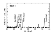
φスキャンにより面内配向を調べたところ、窒化ガリウム層上のアナターゼ相が12回対称のエピタキシャル配向関係を有して成長しているだけでなく、ルチル相も6回対称のエピタキシャル配向関係を有して成長していることが確認された。ただし、ルチル相の強度は、アナターゼ相と比較して弱いことが判明した。すなわち、実質的に、主相はアナターゼ相であることが確認された。
なお、この積層体の比抵抗は、4.3×10⁻⁴Ω・cm、波長460nmの屈折率は2.6であった。また、ホール測定の結果では、キャリア移動度は200cm2V-1s-1未満であり、キャリアである電子の移動度が特異的に高くなる現象はみられなかった。 As a result of examining the crystallinity of the transparent conductive film by X-ray diffraction measurement, as shown in FIG. 5, it was confirmed that the film was a crystalline film composed of an anatase phase and a rutile phase. Thus, it has been found that the crystal has grown with an epitaxial orientation relationship of 12-fold symmetry and 6-fold symmetry. The gallium oxide thin film was confirmed to be crystalline as in Example 7.
When the in-plane orientation was examined by φ scan, not only the anatase phase on the gallium nitride layer grew with a 12-fold symmetry but also the rutile phase had a 6-fold orientation. It was confirmed that it was growing. However, it was found that the strength of the rutile phase was weaker than that of the anatase phase. That is, it was substantially confirmed that the main phase was an anatase phase.
The specific resistance of this laminate was 4.3 × 10 −4 Ω · cm, and the refractive index at a wavelength of 460 nm was 2.6. As a result of the hole measurement, the carrier mobility was less than 200 cm 2 V −1 s −1 , and there was no phenomenon that the mobility of electrons as carriers was specifically increased.
アナターゼ相の(104)面の回折を調べた結果、窒化ガリウム層上のアナターゼ相(A-TiO2{104}で示されるピーク)は12回対称のエピタキシャル配向関係を有して成長していることが明らかである。これに対して、窒化ガリウム層上のルチル相(R-TiO2{110}で示されるピーク)は6回対称のエピタキシャル配向関係を有しているものの、その強度は、縦軸がLogスケールであることを考慮すれば、アナターゼ相と比較して弱いことがわかる。すなわち、実質的に、主相はアナターゼ相であることが確認された。 FIG. 7 shows the result of examining the in-plane orientation by φ scan.
As a result of examining the diffraction of the (104) plane of the anatase phase, the anatase phase (the peak indicated by A-TiO 2 {104}) on the gallium nitride layer grows with a 12-fold symmetric epitaxial orientation relationship. It is clear. In contrast, the rutile phase on the gallium nitride layer (the peak indicated by R—TiO 2 {110}) has a six-fold symmetrical epitaxial orientation relationship, but the intensity is in the log scale on the vertical axis. Considering the fact, it can be seen that it is weaker than the anatase phase. That is, it was substantially confirmed that the main phase was an anatase phase.
このように特異的に高いキャリア移動度はヘテロ構造に由来するものと予想されたため、XPS測定(X線光電子分光測定)によりバンド図を調べた。その結果、ヘテロ接合されたアナターゼ相TiO2薄膜/(酸化ガリウム薄膜/)窒化ガリウム層界面ごく近傍の窒化ガリウム層側において、フェルミレベルが伝導帯に対してスパイク形状をとって局部的に落ち込むように低くなり、その落ち込み部分に二次元的な電子ガスが集積して高速に電子が移動する現象が起こっていることが特定された。この現象により、特異的に高いキャリア移動度が実現したと考えられる。 Next, hole measurement was performed on the laminated body having the heterostructure. As a result, the specific resistance at room temperature is 3.6 × 10 −4 Ω · cm, and the carrier mobility at this time is 260 cm 2 V −1 s −1 and is 200 cm 2 V −1 s −1 or more. It was revealed that the mobility of electrons as carriers is specifically high.
Since the specifically high carrier mobility was expected to be derived from the heterostructure, the band diagram was examined by XPS measurement (X-ray photoelectron spectroscopy measurement). As a result, on the gallium nitride layer side very close to the heterojunction anatase phase TiO 2 thin film / (gallium oxide thin film /) gallium nitride layer interface, the Fermi level seems to fall locally in a spike shape with respect to the conduction band. It has been determined that a phenomenon occurs in which two-dimensional electron gas accumulates in the depressed portion and electrons move at high speed. This phenomenon is considered to have realized a specifically high carrier mobility.
ガラス基板上に直接、酸化チタンを主成分とし、ニオブを含む透明導電膜を成膜し、その成膜条件を、アルゴンと酸素の混合ガスからなるスパッタリングガス中の酸素比率を0.02%、ガス圧を5Paに変更した以外は、実施例1と同様のプロセスによって積層膜を形成した。 (Comparative Example 1)
A transparent conductive film containing titanium oxide as a main component and containing niobium is directly formed on a glass substrate, and the film forming conditions are set such that the oxygen ratio in a sputtering gas composed of a mixed gas of argon and oxygen is 0.02%, A laminated film was formed by the same process as in Example 1 except that the gas pressure was changed to 5 Pa.
X線回折測定によって膜の結晶性を調べた結果、図5に示すように、実施例1とは異なり、ルチル相のみからなる結晶質の膜であることを確認した。 The specific resistance of the obtained transparent conductive film was 2.1 × 10 −2 Ω · cm, which was higher than that of Example 1. The refractive index at a wavelength of 460 nm was 2.6.
As a result of examining the crystallinity of the film by X-ray diffraction measurement, as shown in FIG. 5, unlike Example 1, it was confirmed that the film was a crystalline film composed of only a rutile phase.
GaNテンプレートの表面に酸処理を施して自然酸化膜を除去した後、直接この上に、実施例7と同様のプロセスによって、酸化チタンを主成分としニオブを含む透明導電膜層を形成することにより積層膜を形成した。 (Comparative Example 2)
After removing the natural oxide film by subjecting the surface of the GaN template to acid treatment, a transparent conductive film layer containing titanium oxide as a main component and containing niobium is directly formed on the surface by the same process as in Example 7. A laminated film was formed.
この積層体の比抵抗は4.5×10⁻²Ω・cm、波長460nmの屈折率は2.6であった。また、ホール測定の結果では、キャリア移動度は200cm2V-1s-1未満であり、キャリアである電子の移動度が特異的に高くなる現象はみられなかった。 As a result of examining the crystallinity of the transparent conductive film by X-ray diffraction measurement, it was confirmed that the film was a crystalline film composed of a rutile phase, and the rutile phase on the gallium nitride layer has a six-fold symmetrical epitaxial orientation relationship. It was growing up.
The laminate had a specific resistance of 4.5 × 10 −2 Ω · cm and a refractive index of 2.6 at a wavelength of 460 nm. As a result of the hole measurement, the carrier mobility was less than 200 cm 2 V −1 s −1 , and there was no phenomenon that the mobility of electrons as carriers was specifically increased.
〔窒化ガリウム系化合物半導体層の製造〕
すなわち、サファイアのc面((0001)結晶面)からなる基板上に、AlNからなるバッファー層を介して、アンドープGaN下地層(層厚2000nm)、Siドープn型GaNコンタクト層(層厚2000nm、キャリア濃度=1×1019cm-3)、Siドープn型Al0.07Ga0.93Nクラッド層(層厚12.5nm、キャリア濃度=1×1018cm-3)、6層のSiドープGaN障壁層(層厚14.0nm、キャリア濃度=1×1018cm-3)と5層のアンドープIn0.20Ga0.80Nの井戸層(層厚2.5nm)とからなる多重量子構造の発光層、Mgドープp型Al0.07Ga0.93Nクラッド層(層厚10nm)、およびMgドープp型GaNコンタクト層(層厚100nm)を順次積層した。なお、上記窒化ガリウム系化合物半導体層の積層構造体の各構成層は、MOVEP法で成長させた。 A semiconductor light emitting device was produced by the process as shown below.
[Manufacture of gallium nitride compound semiconductor layers]
That is, an undoped GaN underlayer (layer thickness 2000 nm), a Si-doped n-type GaN contact layer (layer thickness 2000 nm, through a buffer layer made of AlN on a substrate made of c-plane ((0001) crystal plane) of sapphire. Carrier concentration = 1 × 10 19 cm −3 ), Si-doped n-type Al 0.07 Ga 0.93 N clad layer (layer thickness 12.5 nm, carrier concentration = 1 × 10 18 cm −3 ), 6 layers of Si Multiple layers composed of a doped GaN barrier layer (layer thickness 14.0 nm, carrier concentration = 1 × 10 18 cm −3 ) and five undoped In 0.20 Ga 0.80 N well layers (layer thickness 2.5 nm) emitting layer of the quantum structure, Mg-doped p-type Al 0.07 Ga 0.93 N clad layer (
次に、得られた窒化ガリウム系化合物半導体層を用いて、窒化ガリウム系化合物半導体発光素子を作製した。まず、HFおよびHClを用いて、窒化ガリウム系化合物半導体層のp型GaNコンタクト層の表面を洗浄し、そのp型GaNコンタクト層上に、熱酸化処理の温度を500℃に変更したことを除いては、実施例7と同様のプロセスによって、酸化ガリウムからなるバッファー層、続いて酸化チタンを主成分とし、ニオブを含む透明導電膜からなる積層膜を膜厚220nmとなるよう調整して順次成膜した。
その後、上記積層膜を、ドライエッチングを施してパターニングし、p型GaNコンタクト層上の正極形成領域にのみ上記積層膜が形成された状態とした。 [Manufacture of semiconductor light emitting devices]
Next, using the obtained gallium nitride compound semiconductor layer, a gallium nitride compound semiconductor light emitting device was fabricated. First, the surface of the p-type GaN contact layer of the gallium nitride-based compound semiconductor layer is cleaned using HF and HCl, and the temperature of the thermal oxidation treatment is changed to 500 ° C. on the p-type GaN contact layer. In the same manner as in Example 7, a buffer layer made of gallium oxide, and subsequently a laminated film made of a transparent conductive film containing titanium oxide as a main component and containing niobium were adjusted so as to have a film thickness of 220 nm. Filmed.
Thereafter, the laminated film was subjected to dry etching and patterned, so that the laminated film was formed only in the positive electrode formation region on the p-type GaN contact layer.
このようにして得られた半導体発光素子(チップ)を、リードフレーム上に載置し、金(Au)線でリードフレームと結線した。そして、プローブ針によって通電し、発光波長および発光出力を一般的な積分球で測定した。
半導体発光素子の発光面の発光分布は、正極の全面で発光しており、460nm付近の波長領域に発光波長を有していることが確認された。また、発光効率は、正極にITO膜を用いた場合と比較して、15%向上していることを確認した。 [Measurement of emission wavelength and emission output]
The semiconductor light emitting device (chip) thus obtained was placed on a lead frame and connected to the lead frame with a gold (Au) wire. And it supplied with electricity with the probe needle | hook, and measured the light emission wavelength and the light emission output with the common integrating sphere.
The light emission distribution of the light emitting surface of the semiconductor light emitting device was confirmed to emit light over the entire surface of the positive electrode and to have a light emission wavelength in the wavelength region near 460 nm. In addition, it was confirmed that the luminous efficiency was improved by 15% compared to the case where an ITO film was used for the positive electrode.
φスキャンを実施したところ、主相はアナターゼ相であり、ルチル相が少量含まれる点は実施例9と同様であった。また、バッファー層は、TEM観察の結果、非晶質ではなく結晶質であり、β-Ga2O3構造をとることを確認した。 When the obtained transparent conductive film was examined, the electric characteristics and optical characteristics were the same as those in Example 9. In particular, regarding the electric characteristics, a phenomenon in which electrons move at a high speed derived from the heterostructure was confirmed. That is, as a result of hole measurement, the carrier mobility was 200 cm 2 V −1 s −1 or more. The film structure was also found to be anatase phase having the same epitaxial orientation relationship as in Example 9.
When φ scan was performed, the main phase was anatase phase, and a small amount of rutile phase was contained in the same manner as in Example 9. As a result of TEM observation, it was confirmed that the buffer layer was not amorphous but crystalline and had a β-Ga 2 O 3 structure.
膜の構造についても、実施例9と同様のエピタキシャル配向関係を有したアナターゼ相であることが判明した。φスキャンを実施したところ、主相はアナターゼ相であり、ルチル相が少量含まれる点は実施例9と同様であった。また、バッファー層は、TEM観察の結果、非晶質ではなく結晶質であり、β-Ga2O3構造をとることを確認した。 When the obtained transparent conductive film was examined, the electric characteristics and optical characteristics were the same as those in Example 9. In particular, regarding the electric characteristics, a phenomenon in which electrons move at a high speed derived from the heterostructure was confirmed. That is, as a result of hole measurement, the carrier mobility was 200 cm 2 V −1 s −1 or more.
The film structure was also found to be anatase phase having the same epitaxial orientation relationship as in Example 9. When φ scan was performed, the main phase was anatase phase, and a small amount of rutile phase was contained in the same manner as in Example 9. As a result of TEM observation, it was confirmed that the buffer layer was not amorphous but crystalline and had a β-Ga 2 O 3 structure.
φスキャンにより面内配向を調べたところ、アナターゼ相の(104)面の回折から、窒化ガリウム層上のアナターゼ相(A-TiO2{104})は12回対称のエピタキシャル配向関係を有して成長しており、窒化ガリウム層上のルチル相(R-TiO2{110})は6回対称のエピタキシャル配向関係を有していることが判明した。ものの、その強度は、縦軸がLogスケールであることを考慮すれば、アナターゼ相と比較して弱いことがわかる。すなわち、実質的に、主相はアナターゼ相であることが確認された。 As a result of examining the crystallinity of the transparent conductive film by X-ray diffraction measurement, it was confirmed that the transparent conductive film was a crystalline film composed of an anatase phase and a rutile phase. It was found that the crystals grew with a rotationally symmetric epitaxial orientation relationship. The gallium oxide thin film was confirmed to be crystalline as in Example 7.
When the in-plane orientation was examined by φ scan, the anatase phase (A-TiO 2 {104}) on the gallium nitride layer has a 12-fold symmetrical epitaxial orientation relationship based on the diffraction of the (104) plane of the anatase phase. It has been found that the rutile phase (R—TiO 2 {110}) on the gallium nitride layer has a six-fold symmetric epitaxial orientation relationship. However, the intensity is weaker than that of the anatase phase, considering that the vertical axis is the Log scale. That is, it was substantially confirmed that the main phase was an anatase phase.
次に、この積層体の比抵抗を測定したところ、4.2×10⁻⁴Ω・cmであった。ただし、ホール測定の結果では、キャリア移動度は200cm2V-1s-1未満であり、キャリアである電子の移動度が特異的に高くなる現象はみられなかった。 When the refractive index of the transparent conductive film containing titanium oxide as a main component and containing niobium was measured with a spectroscopic ellipsometer, the refractive index at a wavelength of 460 nm was 2.6.
Next, the specific resistance of this laminate was measured and found to be 4.2 × 10 −4 Ω · cm. However, as a result of the hole measurement, the carrier mobility was less than 200 cm 2 V −1 s −1 , and the phenomenon that the mobility of electrons as carriers was specifically increased was not observed.
次に、このヘテロ構造を有する積層体についてホール測定を実施した。その結果、比抵抗は3.0×10⁻⁴Ω・cmであり、このときキャリア移動度は200cm2V-1s-1以上で、キャリアである電子の移動度が特異的に高いことが明らかとなった。 When the refractive index of the transparent conductive film containing titanium oxide as a main component and containing niobium was measured with a spectroscopic ellipsometer, the refractive index at a wavelength of 460 nm was 2.5.
Next, hole measurement was performed on the laminated body having the heterostructure. As a result, the specific resistance is 3.0 × 10 −4 Ω · cm. At this time, the carrier mobility is 200 cm 2 V −1 s −1 or more, and the mobility of electrons as carriers is specifically high. It became clear.
バッファー層である酸化ガリウム薄膜の膜厚が0.05nmであること以外は、実施例9と同様に、GaNテンプレートの表面に酸処理を施して自然酸化膜を除去した後、ヘリコン波励起プラズマスパッタ法を用いて、酸化ガリウム薄膜からなるバッファー層、続けてこの上に、酸化チタンを主成分としニオブを含む透明導電膜層を形成することにより積層膜を形成した。 (Comparative Example 3)
Except that the film thickness of the gallium oxide thin film that is the buffer layer is 0.05 nm, the surface of the GaN template is subjected to acid treatment to remove the natural oxide film, and then the helicon wave excited plasma sputtering is performed. Using this method, a laminated film was formed by forming a buffer layer made of a gallium oxide thin film and subsequently forming a transparent conductive film layer containing titanium oxide as a main component and containing niobium thereon.
次に、この積層体の比抵抗を測定したところ、4.2×10⁻²Ω・cmの高抵抗を示した。また、波長460nmの屈折率は2.6であった。ホール測定の結果では、キャリア移動度は200cm2V-1s-1未満であり、キャリアである電子の移動度が特異的に高くなる現象はみられなかった。 As a result of examining the crystallinity of the transparent conductive film by X-ray diffraction measurement, it was confirmed that the film was a crystalline film composed of a rutile phase, and grew with a 6-fold symmetric epitaxial orientation relationship with the gallium nitride layer. Turned out to be.
Next, when the specific resistance of this laminate was measured, it showed a high resistance of 4.2 × 10 −2 Ω · cm. The refractive index at a wavelength of 460 nm was 2.6. As a result of the hole measurement, the carrier mobility was less than 200 cm 2 V −1 s −1 , and there was no phenomenon that the mobility of electrons as carriers was specifically increased.

すなわち、実施例8では、実施例7と同様に、熱酸化によって形成されたβ-Ga2O3構造をもつ結晶質の酸化ガリウム薄膜の効果によって、本来ルチル相が形成される成膜条件であっても、アナターゼ相が主相として形成されるようになり、しかも12回対称のエピタキシャル配向関係を有して成長していることは明らかである。 However, in Example 8, even when a transparent conductive film is formed under the same conditions, two phases of an anatase phase and a rutile phase are formed, and it can be seen from the result of X-ray diffraction measurement that the anatase phase is dominant.
That is, in Example 8, as in Example 7, under the film forming conditions in which a rutile phase is originally formed by the effect of a crystalline gallium oxide thin film having a β-Ga 2 O 3 structure formed by thermal oxidation. Even so, it is clear that the anatase phase is formed as the main phase, and has grown with a 12-fold symmetric epitaxial orientation relationship.
この現象により、特異的に高いキャリア移動度が実現され、結果的に実施例9に見られるように室温における比抵抗は3.6×10⁻⁴Ω・cmの低抵抗を示し、そのキャリア移動度は260cm2V-1s-1であり、キャリアである電子の移動度が200cm2V-1s-1以上と特異的に高いことは明らかである。 Further, as in Examples 9, 10, 12 and 13, a crystalline gallium oxide thin film formed by a sputtering method has these heterostructures when the buffer layer has a thickness of 0.1 to 1 nm. In the band diagram of the laminated body, the Fermi level takes a spike shape with respect to the conduction band on the gallium nitride layer side in the vicinity of the heterojunction anatase phase TiO 2 thin film / (gallium oxide thin film /) gallium nitride layer interface. It becomes low so as to be depressed. From this, it was identified that a phenomenon in which electrons move at high speed due to the accumulation of two-dimensional electron gas in the depressed portion.
Due to this phenomenon, a specific high carrier mobility is realized. As a result, as shown in Example 9, the specific resistance at room temperature shows a low resistance of 3.6 × 10 −4 Ω · cm, and the carrier mobility The degree is 260 cm 2 V −1 s −1 , and it is clear that the mobility of electrons as carriers is as high as 200 cm 2 V −1 s −1 or higher.
10 窒化ガリウム系化合物半導体層
11 基板
12 n型GaN層(n型半導体層)
13 発光層
14 p型GaN層(p型半導体層)
15 第1あるいは第2のバッファー層、ならびに酸化チタンを主成分とする透明導電膜からなる積層体
16 正極ボンディングパッド
17 負極
DESCRIPTION OF SYMBOLS 1 Semiconductor light-emitting
13 Light emitting layer 14 p-type GaN layer (p-type semiconductor layer)
15 Laminated body composed of first or second buffer layer and transparent conductive film mainly composed of
Claims (19)
- 基体上に、酸化ガリウム薄膜、ガリウム、インジウムおよび酸素からなる酸化物薄膜、ならびにガリウム、インジウム、アルミニウムおよび酸素からなる酸化物薄膜の中から選択される少なくとも1種以上からなるバッファー層を有し、該バッファー層上に酸化チタンを主成分とし、ニオブ、タンタル、モリブデン、ヒ素、アンチモン、ならびにタングステンから選択される少なくとも1種以上の元素を含む酸化物薄膜からなる透明導電膜層が形成されていることを特徴とする積層体。 On the substrate, there is a buffer layer made of at least one selected from a gallium oxide thin film, an oxide thin film made of gallium, indium and oxygen, and an oxide thin film made of gallium, indium, aluminum and oxygen, A transparent conductive film layer made of an oxide thin film containing titanium oxide as a main component and containing at least one element selected from niobium, tantalum, molybdenum, arsenic, antimony, and tungsten is formed on the buffer layer. A laminate characterized by the above.
- 前記バッファー層が、酸化窒化ガリウム薄膜、ガリウム、インジウム、酸素及び窒素からなる酸窒化物薄膜、ならびにガリウム、インジウム、アルミニウム、酸素および窒素からなる酸窒化物薄膜の中から選択される少なくとも1種以上からなる酸窒化物薄膜であることを特徴とする請求項1記載の積層体。 The buffer layer is at least one selected from a gallium oxynitride thin film, an oxynitride thin film composed of gallium, indium, oxygen and nitrogen, and an oxynitride thin film composed of gallium, indium, aluminum, oxygen and nitrogen The laminate according to claim 1, wherein the laminate is an oxynitride thin film.
- 酸化チタンを主成分とする前記透明導電膜層が、アナターゼ相を含むことを特徴とする請求項1または2記載の積層体。 The laminate according to claim 1 or 2, wherein the transparent conductive film layer mainly composed of titanium oxide contains an anatase phase.
- 酸化チタンを主成分とする前記透明導電膜層が、アナターゼ相単相からなることを特徴とする請求項1または2記載の積層体。 The laminate according to claim 1, wherein the transparent conductive film layer mainly composed of titanium oxide is composed of a single anatase phase.
- 前記アナターゼ相が、12回対称のエピタキシャル成長していることを特徴とする請求項4記載の積層体。 The laminate according to claim 4, wherein the anatase phase is epitaxially grown with 12-fold symmetry.
- 前記酸化チタンを主成分とし、ニオブを含む酸化物薄膜において、ニオブ含有量がNb/(Ti+Nb)で表される原子数比で0.1~10原子%であることを特徴とする請求項1~5のいずれか1項に記載の積層体。 2. The oxide thin film containing titanium oxide as a main component and containing niobium has a niobium content of 0.1 to 10 atomic% in terms of an atomic ratio represented by Nb / (Ti + Nb). 6. The laminate according to any one of 1 to 5.
- 前記ニオブ含有量が、Nb/(Ti+Nb)で表される原子数比で2~6原子%であることを特徴とする請求項6記載の積層体。 The laminate according to claim 6, wherein the niobium content is 2 to 6 atomic% in terms of an atomic ratio represented by Nb / (Ti + Nb).
- 酸化チタンを主成分とし、タンタルを含む酸化物薄膜において、タンタル含有量がTa/(Ti+Ta)で表される原子数比で0.1~10原子%であることを特徴とする請求項1~5のいずれか1項に記載の積層体。 The oxide thin film containing titanium oxide as a main component and containing tantalum has a tantalum content of 0.1 to 10 atomic% in terms of an atomic ratio represented by Ta / (Ti + Ta). The laminate according to any one of 5.
- 前記タンタル含有量が、Ta/(Ti+Ta)で表される原子数比で3~7原子%であることを特徴とする請求項8記載の積層体。 The laminate according to claim 8, wherein the tantalum content is 3 to 7 atomic% in terms of an atomic ratio represented by Ta / (Ti + Ta).
- 基体の最表面層が、窒化ガリウム層、窒化ガリウムインジウム層、窒化ガリウムインジウムアルミニウム層から選ばれる薄膜層であることを特徴とする請求項1~9のいずれか1項に記載の積層体。 The laminate according to any one of claims 1 to 9, wherein the outermost surface layer of the substrate is a thin film layer selected from a gallium nitride layer, a gallium nitride indium layer, and a gallium indium aluminum nitride layer.
- 前記バッファー層が、結晶質であることを特徴とする請求項1または2記載の積層体。 The laminate according to claim 1 or 2, wherein the buffer layer is crystalline.
- 前記バッファー層が、単斜晶型β-Ga2O3構造の結晶相からなることを特徴とする請求項11記載の積層体。 12. The laminate according to claim 11, wherein the buffer layer is made of a crystal phase having a monoclinic β-Ga 2 O 3 structure.
- 前記バッファー層の厚みが、0.1~50nmであることを特徴とする請求項1または2記載の積層体。 The laminate according to claim 1 or 2, wherein the buffer layer has a thickness of 0.1 to 50 nm.
- 前記バッファー層の厚みが、0.1~1nmであることを特徴とする請求項1または2記載の積層体。 The laminate according to claim 1 or 2, wherein the buffer layer has a thickness of 0.1 to 1 nm.
- 基体上に、酸化ガリウム薄膜、ガリウム、インジウムおよび酸素からなる酸化物薄膜、ならびにガリウム、インジウム、アルミニウムおよび酸素からなる酸化物薄膜の中から選択される少なくとも1種以上からなるバッファー層が形成され、該バッファー層上に酸化チタンを主成分とし、ニオブ、タンタル、モリブデン、ヒ素、アンチモン、ならびにタングステンから選択される少なくとも1種以上の元素を含む酸化物薄膜からなる透明導電膜層が形成されている積層体の製造方法であって、
少なくとも前記透明導電膜がヘリコン波励起プラズマスパッタリング法で成膜されることを特徴とする積層体の製造方法。 A buffer layer made of at least one selected from a gallium oxide thin film, an oxide thin film made of gallium, indium and oxygen, and an oxide thin film made of gallium, indium, aluminum and oxygen is formed on the substrate, A transparent conductive film layer made of an oxide thin film containing titanium oxide as a main component and containing at least one element selected from niobium, tantalum, molybdenum, arsenic, antimony, and tungsten is formed on the buffer layer. A method for producing a laminate,
A method for producing a laminate, wherein at least the transparent conductive film is formed by helicon wave excitation plasma sputtering. - 前記バッファー層が、酸化窒化ガリウム薄膜、ガリウム、インジウム、酸素および窒素からなる酸窒化物薄膜、ならびにガリウム、インジウム、アルミニウム、酸素および窒素からなる酸窒化物薄膜の中から選択される少なくとも1種以上からなる酸窒化物薄膜であることを特徴とする請求項15記載の積層体の製造方法。 The buffer layer is at least one selected from a gallium oxynitride thin film, an oxynitride thin film composed of gallium, indium, oxygen and nitrogen, and an oxynitride thin film composed of gallium, indium, aluminum, oxygen and nitrogen The method for producing a laminate according to claim 15, wherein the thin film is an oxynitride thin film.
- 請求項1~14のいずれか1項に記載の積層体を具備していることを特徴とする機能素子。 A functional element comprising the laminate according to any one of claims 1 to 14.
- 少なくとも発光層である(Al1-x-y-zInxGayBz)N(0≦x≦1、0≦y≦1、0≦z≦1)層を基体の最表面層とし、該(Al1-x-y-zInxGayBz)N層上に、請求項1~14のいずれか1項に記載の積層体を具備することを特徴とする半導体発光素子。 At least the (Al 1-xyz In x Ga y B z ) N (0 ≦ x ≦ 1, 0 ≦ y ≦ 1, 0 ≦ z ≦ 1) layer as the light emitting layer is used as the outermost surface layer of the substrate. A semiconductor light emitting device comprising the laminate according to any one of claims 1 to 14 on the (Al 1-xyz In x Ga y B z ) N layer.
- 少なくとも光電変換層と、該光電変換層上に形成された請求項1~14のいずれか1項に記載の積層体を具備することを特徴とする太陽電池。
A solar cell comprising: at least a photoelectric conversion layer; and the laminate according to any one of claims 1 to 14 formed on the photoelectric conversion layer.
Priority Applications (4)
| Application Number | Priority Date | Filing Date | Title |
|---|---|---|---|
| CN201180011941.XA CN102791475B (en) | 2010-03-02 | 2011-03-01 | Lamilated body and manufacture method thereof and use its function element |
| KR1020127023482A KR101410598B1 (en) | 2010-03-02 | 2011-03-01 | Laminate, method for producing same, and functional element using same |
| EP11750662.6A EP2543507B1 (en) | 2010-03-02 | 2011-03-01 | Laminate, method for producing same, and functional element using same |
| US13/582,571 US9045821B2 (en) | 2010-03-02 | 2011-03-01 | Laminate, method for producing same, and functional element using same |
Applications Claiming Priority (4)
| Application Number | Priority Date | Filing Date | Title |
|---|---|---|---|
| JP2010-045920 | 2010-03-02 | ||
| JP2010045920 | 2010-03-02 | ||
| JP2011-044497 | 2011-03-01 | ||
| JP2011044497A JP5661509B2 (en) | 2010-03-02 | 2011-03-01 | LAMINATE, MANUFACTURING METHOD THEREOF, AND FUNCTIONAL DEVICE USING THE SAME |
Publications (1)
| Publication Number | Publication Date |
|---|---|
| WO2011108552A1 true WO2011108552A1 (en) | 2011-09-09 |
Family
ID=44542202
Family Applications (1)
| Application Number | Title | Priority Date | Filing Date |
|---|---|---|---|
| PCT/JP2011/054659 WO2011108552A1 (en) | 2010-03-02 | 2011-03-01 | Laminate, method for producing same, and functional element using same |
Country Status (7)
| Country | Link |
|---|---|
| US (1) | US9045821B2 (en) |
| EP (1) | EP2543507B1 (en) |
| JP (1) | JP5661509B2 (en) |
| KR (1) | KR101410598B1 (en) |
| CN (1) | CN102791475B (en) |
| TW (1) | TWI484662B (en) |
| WO (1) | WO2011108552A1 (en) |
Cited By (6)
| Publication number | Priority date | Publication date | Assignee | Title |
|---|---|---|---|---|
| WO2013174824A1 (en) * | 2012-05-21 | 2013-11-28 | Helmholtz-Zentrum Dresden - Rossendorf E.V. | Production of transparent conductive titanium dioxide layers, said layers themselves, and use of said layers |
| JP2015099915A (en) * | 2013-10-18 | 2015-05-28 | 日本放送協会 | Photoelectric conversion element and photoelectric conversion element manufacturing method |
| CN104919541A (en) * | 2013-01-16 | 2015-09-16 | 日东电工株式会社 | Transparent conductive film and production method therefor |
| US9570210B2 (en) | 2013-01-16 | 2017-02-14 | Nitto Denko Corporation | Transparent conductive film and production method therefor |
| US9624573B2 (en) | 2013-01-16 | 2017-04-18 | Nitto Denko Corporation | Production method for transparent conductive film |
| US9805837B2 (en) | 2013-01-16 | 2017-10-31 | Nitto Denko Corporation | Transparent conductive film and production method therefor |
Families Citing this family (20)
| Publication number | Priority date | Publication date | Assignee | Title |
|---|---|---|---|---|
| JP2012025996A (en) * | 2010-07-22 | 2012-02-09 | Mes Afty Corp | Forming method of transparent conductive thin film, and forming device of transparent conductive thin film |
| US8894825B2 (en) | 2010-12-17 | 2014-11-25 | Semiconductor Energy Laboratory Co., Ltd. | Sputtering target, method for manufacturing the same, manufacturing semiconductor device |
| CN103579380A (en) | 2012-08-09 | 2014-02-12 | 索尼公司 | Light-receiving or light-emitting component, solar cell, optical sensor and LED |
| JP6265124B2 (en) * | 2012-08-22 | 2018-01-24 | 住友大阪セメント株式会社 | Dye-sensitized solar cell paste, porous light reflecting insulating layer, and dye-sensitized solar cell |
| KR101900820B1 (en) * | 2012-09-18 | 2018-09-20 | 재단법인 포항산업과학연구원 | Compound for transparent electroconductive thin film, method for forming thin film using the same and transparent electroconductive thin film manufacutred thereby |
| US9929310B2 (en) | 2013-03-14 | 2018-03-27 | Applied Materials, Inc. | Oxygen controlled PVD aluminum nitride buffer for gallium nitride-based optoelectronic and electronic devices |
| KR20150031889A (en) * | 2013-09-17 | 2015-03-25 | 엘지이노텍 주식회사 | Solar cell |
| DE102013112785B3 (en) * | 2013-11-19 | 2015-02-26 | Aixatech Gmbh | Method for producing a composite body with at least one functional layer or for further production of electronic or opto-electronic components |
| TWI520362B (en) * | 2014-05-15 | 2016-02-01 | 國立中山大學 | A stacking structure of photoelectric elements |
| KR101723033B1 (en) * | 2014-11-03 | 2017-04-04 | 주식회사 엘지화학 | Precursor for Manufacturing Light Absorbing Layer of Solar Cell and Method for Manufacturing the Same |
| EP3279367B1 (en) * | 2015-03-30 | 2021-12-01 | Tosoh Corporation | Gallium nitride-based sintered compact and method for manufacturing same |
| US10665426B2 (en) * | 2015-10-28 | 2020-05-26 | Applied Materials, Inc. | Methods for thin film material deposition using reactive plasma-free physical vapor deposition |
| US10340416B2 (en) * | 2016-02-26 | 2019-07-02 | Riken | Crystal substrate, ultraviolet light-emitting device, and manufacturing methods therefor |
| JP6245593B1 (en) * | 2016-08-31 | 2017-12-13 | 国立大学法人大阪大学 | Semiconductor device and manufacturing method of semiconductor device |
| JP7132033B2 (en) * | 2018-08-24 | 2022-09-06 | チタン工業株式会社 | Charge adjustment powder and method for producing the same |
| CN109545964B (en) * | 2018-12-14 | 2021-03-19 | 中国科学院上海微系统与信息技术研究所 | Gating material based on oxide ion implantation, gating unit and preparation method of gating material |
| JP7191322B2 (en) * | 2018-12-26 | 2022-12-19 | 国立研究開発法人物質・材料研究機構 | Semiconductor substrate manufacturing method |
| CN111725348B (en) * | 2020-07-03 | 2021-06-01 | 北京科技大学 | High light response TiO2/MoS2Heterojunction visible light detector and preparation |
| KR102489736B1 (en) * | 2021-03-02 | 2023-01-19 | 인하대학교 산학협력단 | Process for production of thin film comprising multiple quantum well structure, thin film comprising multiple quantum well structure and semiconductor device comprising the same |
| CN114695582B (en) * | 2022-06-01 | 2022-09-13 | 陕西半导体先导技术中心有限公司 | Double-peak heterojunction ultraviolet detector and preparation method thereof |
Citations (12)
| Publication number | Priority date | Publication date | Assignee | Title |
|---|---|---|---|---|
| JPH1034798A (en) * | 1996-07-29 | 1998-02-10 | Mitsui Petrochem Ind Ltd | Transparent conductive film |
| JP2002329669A (en) | 2001-04-27 | 2002-11-15 | Japan Science & Technology Corp | Method for forming film, film forming device and semiconductor light-emitting device |
| JP2006016608A (en) | 2004-05-31 | 2006-01-19 | Keiichi Kotaka | Container for charcoal-making furnace |
| WO2006016608A1 (en) * | 2004-08-13 | 2006-02-16 | Kanagawa Academy Of Science And Technology | Transparent conductor, transparent electrode, solar cell, luminescent device and display panel |
| JP2006073189A (en) | 2004-09-02 | 2006-03-16 | Samsung Electronics Co Ltd | Method and apparatus for detecting disk area |
| JP2006228754A (en) * | 2001-07-31 | 2006-08-31 | American Superconductor Corp | Forming method of superconductor and reactor |
| JP2006324512A (en) * | 2005-05-19 | 2006-11-30 | Nippon Telegr & Teleph Corp <Ntt> | Nitride semiconductor thin film and its manufacturing method |
| JP2007210823A (en) * | 2006-02-08 | 2007-08-23 | Sumitomo Metal Mining Co Ltd | Oxide sintered compact, oxide film obtained using the same and transparent substrate containing the same |
| JP2008050677A (en) | 2006-08-28 | 2008-03-06 | Kanagawa Acad Of Sci & Technol | Metal oxide film |
| JP2008084824A (en) | 2006-03-20 | 2008-04-10 | Kanagawa Acad Of Sci & Technol | Manufacturing method of conductor |
| JP2008294306A (en) | 2007-05-25 | 2008-12-04 | Toyoda Gosei Co Ltd | Group iii nitride compound semiconductor light emitting element |
| JP2009231213A (en) | 2008-03-25 | 2009-10-08 | Kanagawa Acad Of Sci & Technol | Conductor and its manufacturing method |
Family Cites Families (11)
| Publication number | Priority date | Publication date | Assignee | Title |
|---|---|---|---|---|
| US5650019A (en) * | 1993-09-30 | 1997-07-22 | Canon Kabushiki Kaisha | Solar cell module having a surface coating material of three-layered structure |
| US5407602A (en) * | 1993-10-27 | 1995-04-18 | At&T Corp. | Transparent conductors comprising gallium-indium-oxide |
| US6693573B1 (en) * | 2003-03-19 | 2004-02-17 | Raytheon Company | Mixed technology MEMS/BiCMOS LC bandpass sigma-delta for direct RF sampling |
| JP4526776B2 (en) * | 2003-04-02 | 2010-08-18 | 株式会社半導体エネルギー研究所 | LIGHT EMITTING DEVICE AND ELECTRONIC DEVICE |
| KR100580634B1 (en) * | 2003-12-24 | 2006-05-16 | 삼성전자주식회사 | light emitting device and method of manufacturing thereof |
| US7968216B2 (en) | 2005-01-08 | 2011-06-28 | Toyoda Gosei Co., Ltd. | Internal gear pump |
| EP2381743A1 (en) | 2006-09-07 | 2011-10-26 | Saint-Gobain Glass France | Substrate for organic electroluminescent device, use and method for manufacturing said substrate, as well as an organic electroluminescent device |
| CN1971949A (en) * | 2006-12-06 | 2007-05-30 | 南京大学 | Novel semiconductor material In-Ga-N surface barrier type solar battery and its preparation method |
| JP5480554B2 (en) * | 2008-08-08 | 2014-04-23 | 株式会社半導体エネルギー研究所 | Semiconductor device |
| US8236599B2 (en) * | 2009-04-09 | 2012-08-07 | State of Oregon acting by and through the State Board of Higher Education | Solution-based process for making inorganic materials |
| US20120055534A1 (en) * | 2010-09-08 | 2012-03-08 | Applied Materials, Inc. | Photovoltaic Devices with High Work-Function TCO Buffer Layers and Methods of Manufacture |
-
2011
- 2011-03-01 JP JP2011044497A patent/JP5661509B2/en not_active Expired - Fee Related
- 2011-03-01 US US13/582,571 patent/US9045821B2/en not_active Expired - Fee Related
- 2011-03-01 CN CN201180011941.XA patent/CN102791475B/en not_active Expired - Fee Related
- 2011-03-01 WO PCT/JP2011/054659 patent/WO2011108552A1/en active Application Filing
- 2011-03-01 KR KR1020127023482A patent/KR101410598B1/en active IP Right Grant
- 2011-03-01 EP EP11750662.6A patent/EP2543507B1/en active Active
- 2011-03-02 TW TW100106863A patent/TWI484662B/en not_active IP Right Cessation
Patent Citations (12)
| Publication number | Priority date | Publication date | Assignee | Title |
|---|---|---|---|---|
| JPH1034798A (en) * | 1996-07-29 | 1998-02-10 | Mitsui Petrochem Ind Ltd | Transparent conductive film |
| JP2002329669A (en) | 2001-04-27 | 2002-11-15 | Japan Science & Technology Corp | Method for forming film, film forming device and semiconductor light-emitting device |
| JP2006228754A (en) * | 2001-07-31 | 2006-08-31 | American Superconductor Corp | Forming method of superconductor and reactor |
| JP2006016608A (en) | 2004-05-31 | 2006-01-19 | Keiichi Kotaka | Container for charcoal-making furnace |
| WO2006016608A1 (en) * | 2004-08-13 | 2006-02-16 | Kanagawa Academy Of Science And Technology | Transparent conductor, transparent electrode, solar cell, luminescent device and display panel |
| JP2006073189A (en) | 2004-09-02 | 2006-03-16 | Samsung Electronics Co Ltd | Method and apparatus for detecting disk area |
| JP2006324512A (en) * | 2005-05-19 | 2006-11-30 | Nippon Telegr & Teleph Corp <Ntt> | Nitride semiconductor thin film and its manufacturing method |
| JP2007210823A (en) * | 2006-02-08 | 2007-08-23 | Sumitomo Metal Mining Co Ltd | Oxide sintered compact, oxide film obtained using the same and transparent substrate containing the same |
| JP2008084824A (en) | 2006-03-20 | 2008-04-10 | Kanagawa Acad Of Sci & Technol | Manufacturing method of conductor |
| JP2008050677A (en) | 2006-08-28 | 2008-03-06 | Kanagawa Acad Of Sci & Technol | Metal oxide film |
| JP2008294306A (en) | 2007-05-25 | 2008-12-04 | Toyoda Gosei Co Ltd | Group iii nitride compound semiconductor light emitting element |
| JP2009231213A (en) | 2008-03-25 | 2009-10-08 | Kanagawa Acad Of Sci & Technol | Conductor and its manufacturing method |
Non-Patent Citations (2)
| Title |
|---|
| "Heteroepitaxial Growth of Rutile Ti02 on GaN (0001) by Pulsed Laser Deposition", JAPANESE JOURNAL OF APPLIED PHYSICS, vol. 44, 2005, pages L1503 - L1505 |
| "Ta-doped Anatase Ti02 Epitaxial Film as Transparent Conducting Oxide", JAPANESE JOURNAL OF APPLIED PHYSICS, vol. 44, 2005, pages L1063 - L1065 |
Cited By (8)
| Publication number | Priority date | Publication date | Assignee | Title |
|---|---|---|---|---|
| WO2013174824A1 (en) * | 2012-05-21 | 2013-11-28 | Helmholtz-Zentrum Dresden - Rossendorf E.V. | Production of transparent conductive titanium dioxide layers, said layers themselves, and use of said layers |
| CN104919541A (en) * | 2013-01-16 | 2015-09-16 | 日东电工株式会社 | Transparent conductive film and production method therefor |
| US9562282B2 (en) | 2013-01-16 | 2017-02-07 | Nitto Denko Corporation | Transparent conductive film and production method therefor |
| US9570210B2 (en) | 2013-01-16 | 2017-02-14 | Nitto Denko Corporation | Transparent conductive film and production method therefor |
| US9624573B2 (en) | 2013-01-16 | 2017-04-18 | Nitto Denko Corporation | Production method for transparent conductive film |
| CN104919541B (en) * | 2013-01-16 | 2017-05-17 | 日东电工株式会社 | Transparent conductive film and production method therefor |
| US9805837B2 (en) | 2013-01-16 | 2017-10-31 | Nitto Denko Corporation | Transparent conductive film and production method therefor |
| JP2015099915A (en) * | 2013-10-18 | 2015-05-28 | 日本放送協会 | Photoelectric conversion element and photoelectric conversion element manufacturing method |
Also Published As
| Publication number | Publication date |
|---|---|
| CN102791475A (en) | 2012-11-21 |
| JP2011201301A (en) | 2011-10-13 |
| KR101410598B1 (en) | 2014-06-24 |
| JP5661509B2 (en) | 2015-01-28 |
| US9045821B2 (en) | 2015-06-02 |
| CN102791475B (en) | 2016-01-20 |
| TWI484662B (en) | 2015-05-11 |
| EP2543507B1 (en) | 2019-08-28 |
| EP2543507A4 (en) | 2017-05-17 |
| US20120325310A1 (en) | 2012-12-27 |
| TW201140882A (en) | 2011-11-16 |
| EP2543507A1 (en) | 2013-01-09 |
| KR20120127640A (en) | 2012-11-22 |
Similar Documents
| Publication | Publication Date | Title |
|---|---|---|
| JP5661509B2 (en) | LAMINATE, MANUFACTURING METHOD THEREOF, AND FUNCTIONAL DEVICE USING THE SAME | |
| JP5102357B2 (en) | Substrate for epitaxial growth of gallium nitride | |
| US9543473B2 (en) | Polycrystalline gallium-nitride self-supporting substrate and light-emitting element using same | |
| TWI417905B (en) | A transparent conductive film and a method for manufacturing the same, and a transparent conductive substrate and a light-emitting device | |
| JP5397369B2 (en) | Semiconductor light emitting device, method for manufacturing the semiconductor light emitting device, and lamp using the semiconductor light emitting device | |
| EP3086378A1 (en) | Composite substrate for light-emitting element and production method therefor | |
| WO2008072681A1 (en) | Compound semiconductor light emitting element and method for producing the compound semiconductor light emitting element | |
| JP6732201B2 (en) | Light emitting element | |
| Zou et al. | Structural, electrical and optical properties of Mg-doped CuAlO 2 films by pulsed laser deposition | |
| KR101758548B1 (en) | Gallium nitride self-supported substrate, light-emitting device and manufacturing method therefor | |
| WO2011132394A1 (en) | Light emitting diode | |
| KR20050081208A (en) | Growth of single nitride-based semiconductors using substrate decomposition prevention layer and manufacturing of high-quality nitride-based light emitting devices | |
| WO2017221863A1 (en) | Group iii nitride laminate and vertical semiconductor device provided with said laminate | |
| EP4057363A1 (en) | Laminate and semiconductor device | |
| JP6890858B2 (en) | Substrate and method for manufacturing the substrate | |
| WO2023074374A1 (en) | Multilayer structure and gallium-nitride-based semiconductor device |
Legal Events
| Date | Code | Title | Description |
|---|---|---|---|
| WWE | Wipo information: entry into national phase |
Ref document number: 201180011941.X Country of ref document: CN |
|
| 121 | Ep: the epo has been informed by wipo that ep was designated in this application |
Ref document number: 11750662 Country of ref document: EP Kind code of ref document: A1 |
|
| NENP | Non-entry into the national phase |
Ref country code: DE |
|
| WWE | Wipo information: entry into national phase |
Ref document number: 13582571 Country of ref document: US |
|
| ENP | Entry into the national phase |
Ref document number: 20127023482 Country of ref document: KR Kind code of ref document: A |
|
| WWE | Wipo information: entry into national phase |
Ref document number: 2011750662 Country of ref document: EP |