WO2011105455A1 - Relief printing plate, printing device using same, thin film manufacturing method, and organic el element manufacturing method - Google Patents
Relief printing plate, printing device using same, thin film manufacturing method, and organic el element manufacturing method Download PDFInfo
- Publication number
- WO2011105455A1 WO2011105455A1 PCT/JP2011/054040 JP2011054040W WO2011105455A1 WO 2011105455 A1 WO2011105455 A1 WO 2011105455A1 JP 2011054040 W JP2011054040 W JP 2011054040W WO 2011105455 A1 WO2011105455 A1 WO 2011105455A1
- Authority
- WO
- WIPO (PCT)
- Prior art keywords
- organic
- ink
- relief printing
- printing plate
- layer
- Prior art date
Links
Images


Classifications
-
- B—PERFORMING OPERATIONS; TRANSPORTING
- B41—PRINTING; LINING MACHINES; TYPEWRITERS; STAMPS
- B41N—PRINTING PLATES OR FOILS; MATERIALS FOR SURFACES USED IN PRINTING MACHINES FOR PRINTING, INKING, DAMPING, OR THE LIKE; PREPARING SUCH SURFACES FOR USE AND CONSERVING THEM
- B41N1/00—Printing plates or foils; Materials therefor
- B41N1/12—Printing plates or foils; Materials therefor non-metallic other than stone, e.g. printing plates or foils comprising inorganic materials in an organic matrix
-
- B—PERFORMING OPERATIONS; TRANSPORTING
- B41—PRINTING; LINING MACHINES; TYPEWRITERS; STAMPS
- B41M—PRINTING, DUPLICATING, MARKING, OR COPYING PROCESSES; COLOUR PRINTING
- B41M1/00—Inking and printing with a printer's forme
- B41M1/02—Letterpress printing, e.g. book printing
-
- H—ELECTRICITY
- H10—SEMICONDUCTOR DEVICES; ELECTRIC SOLID-STATE DEVICES NOT OTHERWISE PROVIDED FOR
- H10K—ORGANIC ELECTRIC SOLID-STATE DEVICES
- H10K71/00—Manufacture or treatment specially adapted for the organic devices covered by this subclass
- H10K71/10—Deposition of organic active material
- H10K71/12—Deposition of organic active material using liquid deposition, e.g. spin coating
- H10K71/13—Deposition of organic active material using liquid deposition, e.g. spin coating using printing techniques, e.g. ink-jet printing or screen printing
Definitions
- the present invention relates to a relief printing plate, a method for producing a thin film using the relief printing plate, a printing apparatus, and a method for producing an organic EL (Electro-Luminescence) element using the relief printing plate.
- printing is usually performed as follows. First, ink is supplied to the entire surface of the cylindrical transfer roll, and then the relief printing plate is pressed against the transfer roll to transfer the ink to the convex portions of the relief printing plate. Further, printing is performed by pressing the relief printing plate against the printing material, and a thin film is formed on the printing material with a predetermined pattern.
- anilox roll is frequently used for the transfer roll described above.
- the anilox roll is a transfer roll having fine irregularities formed on the surface, and the amount of ink transferred to the relief printing plate can be adjusted by adjusting the shape of the irregularities formed on the surface.
- a relief printing method using an anilox roll will be described with reference to FIG.
- FIG. 4 is a diagram schematically showing a relief printing method using an anilox roll.
- Printing ink (ink supply source) 22 is accommodated in an ink tank TK.
- the anilox roll 23 ′ is rotatably supported in a state where a part of the anilox roll 23 ′ is immersed in the ink 22, and rotates counterclockwise as indicated by an arrow in FIG. 4.
- Ink adheres to the surface of the anilox roll 23 ′ that has passed through the ink 22.
- the ink adheres in a larger amount than the amount to be transferred to the relief printing plate 12 ', but the excess ink is removed by a doctor blade DB before being transferred to the relief printing plate 12'.
- a doctor blade DB As shown in FIG.
- the doctor blade DB is pressed against the anilox roll 23 'before the relief printing plate 12' wound around the plate cylinder 24 is pressed against the anilox roll 23 '. This removes excess ink and fills the recesses on the surface of the anilox roll 23 'with the intended amount of ink.
- the relief printing plate 12 ′ is pressed in a state where the intended amount of ink is held on the anilox roll 23 ′, the intended amount of ink is transferred to the relief printing plate, and this is further printed on the printing medium. Is done.
- the ink supplied to the anilox roll is transferred to the relief printing plate, but not all of it is transferred, and a part of the ink remains on the anilox roll without being transferred.
- the ink remaining on the anilox roll moves toward the ink tank as the anilox roll rotates, and is again stored in the ink tank. Since the ink supplied to the anilox roll partially evaporates during the rotation of the anilox roll, the solid content concentration increases. Therefore, ink with a high solid content concentration continues to be stored in the ink tank, and as a result, the ink composition in the ink tank changes with time.
- the ink composition in the ink tank changes as described above, there is a problem that it is difficult to continuously form a thin film having a certain property by the relief printing method using an anilox roll. Although it may be possible to wash the anilox roll to prevent the ink from returning to the ink tank, it is difficult to completely remove the ink filled in the recesses on the surface of the anilox roll. It is difficult to completely prevent the ink from returning to the ink tank.
- the present inventors examined forming a thin film by using a transfer roll having a flat surface instead of an anilox roll having irregularities formed on the surface.
- a transfer roll having a flat surface an intended amount of ink does not adhere to the surface of the transfer roll simply by immersing the transfer roll in the ink. Therefore, the ink is usually supplied to the surface of the transfer roll by a slit coating method or the like.
- the amount of ink transferred from the transfer roll to the relief printing plate can be adjusted to some extent by controlling the amount of ink supplied to the transfer roll, but in reality, only the ink supply amount is adjusted. In this case, the intended amount of ink was not transferred to the relief printing plate, and as a result, a new problem that a thin film having the intended thickness could not be formed was confirmed.
- an object of the present invention is to provide a relief printing plate capable of forming a thin film having a desired film thickness by a relief printing method using a transfer roll having a flat surface, a printing apparatus using the relief printing plate, a method for producing a thin film, And the manufacturing method of an organic EL element is to provide.
- the relief printing plate of the present invention is a relief printing plate used in a relief printing method using a transfer roll having a flat surface, and has a convex portion having a predetermined depression formed on the surface.
- the projection has a plurality of the depressions arranged so as to be point-symmetric.
- the relief printing plate of the present invention has a plurality of the convex portions extending in a predetermined direction at predetermined intervals.
- the convex portion has the depression extending in the predetermined direction or the depression extending in a direction perpendicular to the predetermined direction.
- the printing apparatus of the present invention includes the ink supply source, the transfer roll supplied with the ink from the ink supply source, the surface of the transfer roll, and the relief printing, to which the ink supplied to the surface of the transfer roll is transferred.
- the method for producing a thin film of the present invention includes a step of supplying ink to a transfer roll having a flat surface, a step of pressing the relief printing plate against the transfer roll, and transferring the ink to the relief printing plate, The method includes a step of pressing a relief printing plate against a printing material to print the ink, and a step of solidifying the ink to form a thin film on the printing material.
- the manufacturing method of the organic EL element of this invention is a manufacturing method of an organic EL element provided with a pair of electrodes and the organic EL layer provided between these electrodes, Comprising: One electrode of a pair of electrodes is formed.
- a step of supplying an organic EL ink containing a material to be the organic EL layer to a transfer roll having a flat surface, pressing the relief printing plate against the transfer roll, and applying the organic EL ink to the relief printing A step of transferring to a plate, a step of pressing the relief printing plate against a pair of the electrodes, printing the organic EL ink, and solidifying the organic EL ink to form an organic EL layer on the one electrode And a step of forming the other of the pair of electrodes on the organic EL layer.
- a thin film having a desired film thickness can be formed by a relief printing method using a transfer roll having a flat surface.
- FIG. 1 is a diagram schematically showing a relief printing plate of the present embodiment.
- FIG. 2 is a diagram schematically illustrating a convex portion in which continuous depressions are formed.
- FIG. 3 is a diagram schematically illustrating a printing apparatus including the above-described relief printing plate.
- FIG. 4 is a diagram schematically showing a relief printing method using an anilox roll.
- FIG. 5 is a diagram showing a state of exposure during printing plate preparation.
- FIG. 6 is a diagram showing a state of exposure during printing plate preparation.
- FIG. 7 is a longitudinal sectional view of the organic EL element.
- FIG. 8 is a longitudinal sectional view of the organic EL element.
- FIG. 9 is a longitudinal sectional view of the organic EL element.
- FIG. 10 is a longitudinal sectional view of the organic EL element.
- FIG. 11 is a longitudinal sectional view of the organic EL element.
- FIG. 12 is a longitudinal sectional view of the organic EL element.
- FIG. 13 is a longitudinal sectional view of the organic EL element.
- FIG. 14 is a longitudinal sectional view of the organic EL element.
- FIG. 15 is a longitudinal sectional view of a display device including an organic EL element.
- the relief printing plate of the present invention is a relief printing plate used in a relief printing method using a transfer roll having a flat surface, and has a convex portion having a predetermined depression formed on the surface. Since the preparation is easy, the relief printing plate is preferably made of a resin.
- the amount of ink transferred from the transfer roll can be adjusted by forming a predetermined depression on the surface of the convex portion. Thereby, the film thickness of the printed thin film can be adjusted.
- a convex portion of a pattern corresponding to the pattern of the thin film to be formed on the printing medium is formed.
- a plurality of strip-shaped thin films are formed on a printing medium, a plurality of protrusions extending in a predetermined direction with a predetermined distance from each other so as to correspond to the pattern of the strip-shaped thin film Is provided on the relief printing plate.
- a plurality of convex portions arranged in a matrix so as to correspond to the pattern of the plurality of thin films are provided on the relief printing plate.
- FIG. 1 is a diagram schematically showing a relief printing plate of this embodiment.
- FIG. 1A is a plan view of a relief printing plate
- FIG. 1B is a cross-sectional view thereof.
- a plurality of protrusions 11 extending in a predetermined direction with a predetermined interval from each other, that is, a plurality of protrusions 11 arranged in a stripe shape are formed on the flexible support film 100.
- the made relief printing plate 12 is shown as one embodiment.
- the hollow 14 is hatched.
- a predetermined depression 14 is provided in the convex portion 11 of the relief printing plate 12.
- the shape and arrangement of the recesses 14 are appropriately set according to the amount of ink transferred.
- the amount of ink transferred can be adjusted by appropriately adjusting the ratio of the area of the depressions 14 to the area of the protrusions 11 and the depth of the depressions 14.
- the convex part 11 has a plurality of the depressions 14 arranged so as to be point-symmetric.
- the plurality of depressions 14 are preferably arranged so as to be point-symmetric.
- the depressions 14 are formed in each convex portion 11 so as to be line symmetric with respect to a predetermined symmetry axis whose axial direction coincides with the thickness direction of the relief printing plate 12.
- the relief printing plate 12 is used by being wound around a predetermined plate cylinder.
- the arrangement of the depressions 14 means an arrangement in a state where the relief printing plate 12 is placed on a plane.
- the film thickness of the ink transferred from the transfer roll to the convex portion can be made uniform, and as a result, a thin film with a uniform film thickness is formed on the printing medium. be able to.
- FIG. 1 shows a relief printing plate in which two depressions 14 are provided in the width direction perpendicular to the direction in which each protrusion extends, but the number of depressions in the width direction is not limited to two. It may be one, or three or more.
- the circular depression 14 is shown in plan view, but the shape of the depression 14 in plan view is not limited to a circle, and may be polygonal or substantially elliptical.
- the width direction is also a direction perpendicular to the thickness direction of the substrate.
- FIG. 2 is a diagram schematically showing a convex portion in which continuous depressions are formed.
- one convex part of the convex part formed in multiple numbers is expanded and shown typically. Even if the depressions are continuously formed, the depressions are preferably arranged so as to be point-symmetric.
- the projection 11 is: It is preferable to have a plurality of the recesses extending in the predetermined direction or a plurality of the recesses extending in a direction perpendicular to the predetermined direction. That is, the convex portion is a recess 14 extending in the same direction as the direction in which the convex portion extends as shown in FIG. 2 (A), or the direction in which the convex portion extends as shown in FIG. 2 (B). It is preferable to have a recess 14 extending in the vertical direction. Note that FIG. 2A shows a convex portion in which three dents extending in the same direction as the direction in which the convex portion extends are shown, but the number of dents is not limited to three, but one or more. If it is.
- a lattice-like depression 14 may be formed in the convex portion 11, and as shown in FIG. 2D, the convex portion 11 has a V-shape in plan view. A dent 14 may be formed.
- the relief printing plate 12 of this embodiment can be produced using, for example, a photosensitive resin.
- a photosensitive resin photoresist
- FIG. 5A first, a negative photosensitive resin (photoresist) 11 ′ is formed on a predetermined substrate 100.
- the negative photosensitive resin 11 ′ has a property that when exposed to light, the solubility in the developer is lowered, and the exposed portion remains after development.
- the photosensitive resin 11 ′ is exposed with UV light through the photomask M, and the portion constituting the convex portion 11 is cured.
- the exposure amount is varied.
- FIG. 5B shows a case where only the region (b) corresponding to the depression 14 is exposed.
- the exposure amount of the region ⁇ region (a) ⁇ region (b)> is made larger than that of the region (b).
- the exposure may be performed in two steps. For example, as shown in FIG.
- the region (ab) ⁇ region (a) ⁇ region (b) ⁇ is exposed in the projected portion formation region, and the second time, the region (a) is exposed. What is necessary is just to expose. Since the region (b) is included in the region (a), the exposure amount of the region (b) is lower than the exposure amount of the region (a). Of course, when the exposure amount of the first region (ab) is large, only the region (b) is smaller than the exposure amount (exposure amount per unit area) of the region (ab) in the second time. You may expose by exposure amount (exposure amount per unit area). Then, the uncured photosensitive resin is washed away and developed.
- the region ⁇ region (a) ⁇ region (b)> is hardened more than the region (b) by varying the exposure amount. Therefore, during development, the region ⁇ b> The region ⁇ region (a) -region (b)> remains, in other words, in the region where the projection is to be formed, the region (b) is significantly dissolved from the periphery thereof, so that the depression 14 is formed. The convex part 11 formed in the top surface is obtained. In this way, the relief printing plate 12 can be obtained.
- the exposure may be performed only from the photosensitive resin side. However, when the substrate is transparent to the exposure light, the exposure may be performed in advance from the substrate side.
- photosensitive resin 11 ' for example, polyamide, polyimide, acrylate, or the like can be used.
- substrate 100 polyethylene terephthalate, polyimide, polycarbonate, or the like can be used.
- FIG. 3 is a diagram schematically illustrating a printing apparatus 21 including the relief printing plate 12 described above.
- the printing apparatus 21 mainly includes an ink supply source 22, a transfer roll 23 having a flat surface to which ink is supplied from the ink supply source 22, and the ink supplied to the surface of the transfer roll 23.
- the relief printing plate 12 is provided.
- the relief printing plate 12 is usually used by being wound around the plate cylinder 24.
- the relief printing plate should be such that the direction in which the projections extend matches the circumferential direction of the plate cylinder, or the direction in which the projections extend. Is wound around the plate cylinder so as to coincide with the axial direction of the plate cylinder.
- the plate cylinder 24 is rotatably supported around the axis CR1 and is rotated by a driving force from the rotation driving mechanism DRV1. In FIG. 3, the plate cylinder 24 rotates clockwise as indicated by an arrow, and the relief printing plate 12 also rotates as the plate cylinder 24 rotates.
- the transfer roll 23 is rotatably supported so that its axis CR2 is parallel to the axis of the plate cylinder 24, and rotates by the driving force from the rotation driving mechanism DRV2. In FIG. 3, as indicated by an arrow, the transfer roll 23 rotates counterclockwise.
- the transfer roll 23 is made of, for example, chromium, chromium oxide, aluminum, aluminum oxide, or the like.
- the ink supply source 22 stores ink and supplies it to the transfer roll 23.
- the slit nozzle 25 is used to supply ink to the transfer roll 23.
- the printing apparatus further includes a cleaning mechanism 26.
- the cleaning mechanism 26 cleans the ink remaining on the transfer roll 23 after the ink is transferred from the transfer roll 23 to the relief printing plate 12.
- the cleaning mechanism 26 includes a doctor blade, and scrapes ink remaining on the transfer roll 23 by pressing the doctor blade against the transfer roll 23.
- the transfer roll 23 may be washed using a predetermined rinse liquid.
- the printing apparatus 21 further includes a transport table 28 that transports the printing medium 27.
- the transport table 28 holds the printing material 27 and moves in parallel to the tangential direction of the relief printing plate 12 at the same speed as the tangential velocity of the relief printing plate 12.
- the transfer table 28 normally moves horizontally. As the transport table 28 moves, the printing medium also moves in parallel.
- the ink supplied from the ink supply source 22 is supplied onto the transfer roll 23 through the slit nozzle 25.
- the ink roll is rotated while the ink is supplied from the slit nozzle 25, whereby an ink thin film is formed on the surface of the transfer roll 23.
- the surface of the transfer roll 23 is flat (smooth).
- the root mean square roughness (RMS) of the surface of the transfer roll 23 is significantly smaller than the RMS of the surface of the relief printing plate 12 having irregularities.
- the ink supplied to the transfer roll 23 is sequentially transferred onto the surface of the projection of the relief printing plate 12.
- the relief printing plate 12 to which the ink is transferred and holds the ink on the convex portion rotates while being pressed against the printing medium 27. Since the printing medium 27 moves in parallel with the rotation of the relief printing plate 12, the ink held on the convex portions of the relief printing plate 12 is sequentially printed on the printing medium 27.
- the ink remaining on the transfer roll 23 without being transferred to the relief printing plate 12 is removed from the transfer roll 23 by the cleaning mechanism 26.
- the step of supplying ink to a transfer roll having a flat surface the step of pressing the above-described relief printing plate against the transfer roll, transferring the ink to the relief printing plate, and printing the relief printing plate And a step of printing the ink on the body, and further solidifying the ink to form a thin film of ink on the substrate, thereby forming a thin film on the substrate .
- the ink can be solidified by removing the solvent.
- the removal of the solvent is performed by, for example, natural drying, heat drying, vacuum drying, or the like.
- the ink may be solidified by irradiating light or applying heat after the ink is printed on the printing medium. .
- an intended amount of ink can be transferred to the relief printing plate 12 by forming the predetermined depressions 14 in the projections 11.
- an intended amount of ink can be printed on the printing medium 27, and as a result, a thin film having an intended thickness can be formed on the printing medium.
- a conductive thin film functioning as an electrode or a wiring, an active layer of an organic photoelectric conversion element, a semiconductor layer of an organic thin film transistor, and an organic EL layer of an organic EL element described later can be formed. it can.
- the manufacturing method of the organic EL element 1 of the present embodiment is a manufacturing method of an organic EL element including a pair of electrodes 2 and 5 and an organic EL layer 10 provided between the electrodes as shown in FIG.
- the above-described relief printing plate 12 is pressed against the transfer roll 23 to transfer the organic EL ink to the relief printing plate 12, and the relief printing plate 12 is pressed against the pair of one electrode 2 to print the organic EL ink.
- the step of solidifying the organic EL ink, forming the organic EL layer (particularly the light emitting layer 4) 10 on one electrode 2, and the other electrode 5 of the pair of electrodes on the organic EL layer 10 Forming an organic EL Child process for the preparation of.
- the organic EL element 1 is used as a pixel of a display device, for example.
- a plurality of organic EL elements 1 are arranged on a support substrate 6 in a predetermined arrangement.
- the plurality of organic EL elements 1 are arranged in a matrix on the support substrate 6. That is, the plurality of organic EL elements 1 are arranged in a line with a predetermined interval in a predetermined row direction and with a predetermined interval in a predetermined column direction.
- a partition wall IW for separating a plurality of organic EL elements is usually provided on the support substrate 6.
- the plurality of organic EL elements are respectively formed in regions divided by the partition walls IW.
- the partition wall IW is provided in a stripe shape or a lattice shape, for example.
- a plurality of partition walls extending in a predetermined direction are provided on the substrate at predetermined intervals.
- each organic EL element 1 is provided between each partition IW, and is arrange
- Organic EL element 1 includes a pair of electrodes 2 and 5.
- the pair of electrodes includes an anode and a cathode. That is, one of the pair of electrodes functions as one of the anode and the cathode, and the other of the pair of electrodes serves as the other of the anode and the cathode. Function.
- one electrode 2 of each organic EL element is formed on the support substrate 6. That is, one electrode 2 having a number corresponding to the number of organic EL elements 1 is formed on the support substrate 6.
- the plurality of one electrodes 2 are arranged in a matrix in a plan view.
- a stripe-shaped partition wall IW is formed.
- a stripe-shaped partition is formed between one adjacent electrode 2 and 2.
- the partition wall IW can be formed by a photolithography method using, for example, a photosensitive resin.
- the organic EL layer 10 is formed.
- an organic EL ink containing a material to be the organic EL layer 10 is supplied between the stripe-shaped partition walls IW, and further solidified to thereby form a strip-shaped organic EL layer between the stripe-shaped partition walls IW.
- the organic EL ink is supplied between the stripe-shaped partition walls IW by the above-described relief printing method. That is, in the above-described relief printing method, an organic EL ink containing a material that becomes an organic EL layer is used as the ink. Further, as the relief printing plate 12, stripe-like projections 11 corresponding to the pattern between the partition walls IW and IW are used. The letterpress printing plate 12 on which is formed is used.
- the solvent or dispersion medium of the organic EL ink may be any solvent that uniformly dissolves or disperses the material that becomes the organic EL layer.
- chlorinated solvents such as chloroform, methylene chloride, dichloroethane, ether solvents such as tetrahydrofuran, aromatic hydrocarbon solvents such as toluene and xylene, ketone solvents such as acetone and methyl ethyl ketone, ethyl acetate, butyl acetate, and ethyl cellosolve
- ether solvents such as tetrahydrofuran
- aromatic hydrocarbon solvents such as toluene and xylene
- ketone solvents such as acetone and methyl ethyl ketone
- ethyl acetate ethyl acetate
- butyl acetate ethyl cellosolve
- An ester solvent such as acetate and water can be appropriately used as a solvent or a dispersion medium.
- the film thickness of the organic EL layer 10 is usually about 30 nm to 120 nm. Since the characteristics of the organic EL element 1 greatly depend on the film thickness of the organic EL layer 10, it is desired to form an organic EL layer having an intended film thickness. In the present embodiment, an intended amount of organic EL ink can be supplied between the partition walls IW and IW by forming a predetermined depression in the convex portion 11 of the relief printing plate 12, and as a result, the intended film thickness is obtained. The organic EL layer 10 can be formed. Thereby, the organic EL element 1 having desired characteristics can be formed.
- the organic EL layer means all layers provided between a pair of electrodes. At least one light emitting layer 4 is provided as an organic EL layer between the pair of electrodes (see FIG. 14).
- At least one organic EL layer is formed by the relief printing method of the present invention described above.
- the organic EL layer that can be formed by a coating method is preferably formed by the relief printing method of the present invention described above.
- the organic EL ink of each color can be applied separately by forming the pattern of the convex portion 11 of the printing plate so as to correspond to the pattern to which the organic EL ink of each color is supplied.
- the other electrode 5 is formed on the organic EL layer.
- a plurality of organic EL layers 10 are formed on the substrate 6 as shown in FIG.
- a vacuum deposition method, a sputtering method, an ion plating method, a lamination method, or a plating method can be used.
- the method of forming the plurality of organic EL elements 1 on the substrate 6 on which the stripe-shaped partition walls IW are formed has been described.
- the plurality of organic EL elements are formed on the substrate on which the lattice-shaped partition walls are formed.
- the organic EL layer of each organic EL element can be formed by the relief printing method mentioned above.
- a relief printing plate in which a plurality of projections arranged in a matrix form is used so as to correspond to the matrix pattern divided by the grid-like partition walls may be used.
- the organic EL element can have various layer configurations.
- the layer structure of the organic EL element, the configuration of each layer, and the method for forming each layer will be described in more detail below.
- the organic EL element includes a pair of electrodes 2 and 5 and one or a plurality of organic EL layers 10 provided between the electrodes 2 and 5, and at least one layer of light emission as one or a plurality of organic EL layers.
- the organic EL element may include a layer containing an inorganic substance and an organic substance, an inorganic layer, and the like.
- the organic substance constituting the organic layer may be a low molecular compound or a high molecular compound, or a mixture of a low molecular compound and a high molecular compound.
- the organic layer preferably contains a polymer compound, and preferably contains a polymer compound having a polystyrene-equivalent number average molecular weight of 10 3 to 10 8 .
- Examples of the organic EL layer provided between the cathode and the light emitting layer include an electron injection layer, an electron transport layer, and a hole blocking layer.
- the layer close to the cathode is called an electron injection layer
- the layer close to the light emitting layer is called an electron transport layer.
- Examples of the organic EL layer provided between the anode and the light emitting layer include a hole injection layer, a hole transport layer, and an electron block layer.
- the organic EL element can include a predetermined layer in addition to the light emitting layer between the pair of electrodes as described above.
- Examples of the organic layer 10 formed between the electrode (anode) 2 and the electrode (cathode) 5 formed on the support substrate 6 include the following structures.
- the organic EL element has an organic layer Y between the electrode (anode) 2 and the light emitting layer 4 and an organic layer between the electrode (cathode) 5 and the light emitting layer 4. It can be set as the structure where the layer X interposes.
- the organic EL element has a structure in which an organic layer Y is interposed between the electrode (anode) 2 and the light emitting layer 4, and the electrode 5 is formed directly on the light emitting layer 4. It can be set as a structure.
- the organic layer X is interposed between the electrode (cathode) 5 and the light emitting layer 4, and the light emitting layer 4 is in direct contact with the electrode 2. It can be.
- the organic layer X may be composed of two or more kinds of organic layers X1 and X2 as shown in FIG. 10, and the organic layer Y is composed of two or more kinds of organic layers Y1 and Y2 as shown in FIG. It may be.
- only the light emitting layer 4 may be formed between the anode 2 and the cathode 5 as shown in FIG.
- Examples of the layer X provided between the cathode 5 and the light emitting layer 4 include an electron injection layer, an electron transport layer, and a hole blocking layer. As shown in FIG. 10, when both the electron injection layer X1 and the electron transport layer X2 are provided between the cathode 5 and the light emitting layer 4, the layer in contact with the cathode 5 is referred to as the electron injection layer X1, The layer excluding the electron injection layer X1 is referred to as an electron transport layer X2.
- the electron injection layer has a function of improving the electron injection efficiency from the cathode.
- the electron transport layer has a function of improving electron injection from the layer in contact with the surface on the cathode side.
- the hole blocking layer has a function of blocking hole transport. In the case where the electron injection layer and / or the electron transport layer have a function of blocking hole transport, these layers may also serve as the hole blocking layer.
- the hole blocking layer has a function of blocking hole transport makes it possible, for example, to produce an element that allows only hole current to flow, and confirm the blocking effect by reducing the current value.
- Examples of the layer Y provided between the anode 2 and the light emitting layer 4 include a hole injection layer, a hole transport layer, and an electron block layer. As shown in FIG. 11, when both the hole injection layer Y1 and the hole transport layer Y2 are provided between the anode 2 and the light emitting layer 4, the layer in contact with the anode 2 is the hole injection layer.
- the layer excluding the hole injection layer Y1 is referred to as Y1, and is referred to as a hole transport layer Y2.
- the hole injection layer has a function of improving the hole injection efficiency from the anode.
- the hole transport layer has a function of improving hole injection from a layer in contact with the surface on the anode side.
- the electron blocking layer has a function of blocking electron transport. In the case where the hole injection layer and / or the hole transport layer has a function of blocking electron transport, these layers may also serve as an electron blocking layer.
- the electron blocking layer has a function of blocking electron transport makes it possible, for example, to produce an element that allows only electron current to flow, and confirm the blocking effect by reducing the current value.
- the electron injection layer and the hole injection layer are sometimes collectively referred to as a charge injection layer, and the electron transport layer and the hole transport layer are sometimes collectively referred to as a charge transport layer.
- An example of a layer structure that can be taken by the organic EL element of the present embodiment is shown below. a) Anode 2 / light emitting layer 4 / cathode 5 (see FIG. 14) b) Anode 2 / hole injection layer Y / light emitting layer 4 / cathode 5 (see FIG. 8) c) Anode 2 / hole injection layer Y / light emitting layer 4 / electron injection layer X / cathode 5 (see FIG.
- the organic EL element of the present embodiment may have two or more light emitting layers.
- the configuration of the organic EL device having two light emitting layers is as follows. And the layer structure shown in the following q).
- the two (structural unit A) layer structures may be the same or different.
- Anode 2 / (structural unit A) / charge generation layer Z / (structural unit A) / cathode 5 see FIG. 12
- examples of the configuration of the organic EL element having three or more light emitting layers include the layer configuration shown in the following r).
- Anode 2 / (structural unit B) x / (structural unit A) / cathode 5 see FIG. 13
- the symbol “x” represents an integer of 2 or more
- (structural unit B) x represents a stacked body in which the structural unit B is stacked in x stages.
- a plurality of (structural units B) may have the same or different layer structure.
- the charge generation layer Z is a layer that generates holes and electrons by applying an electric field.
- Examples of the charge generation layer Z include a thin film made of vanadium oxide, indium tin oxide (IndiumInTin Oxide: abbreviated as ITO), molybdenum oxide, or the like.
- Organic EL element is usually provided on a support substrate.
- the organic EL element may be provided on the support substrate with the anode of the pair of electrodes including the anode and the cathode disposed closer to the support substrate than the cathode, and the cathode is disposed closer to the support substrate than the anode. May be provided on the support substrate.
- an organic EL element having a structure in which each layer is stacked on the support substrate in order from the right side or an organic EL element having a structure in which each layer is stacked on the support substrate from the left side may be used. .
- the order of the layers to be laminated, the number of layers, and the thickness of each layer can be appropriately set in consideration of light emission efficiency and element lifetime.
- an electrode exhibiting optical transparency is used for the anode.
- the electrode exhibiting light transmittance a thin film of metal oxide, metal sulfide, metal or the like can be used, and an electrode having high electrical conductivity and light transmittance is preferably used.
- a thin film made of indium oxide, zinc oxide, tin oxide, ITO, indium zinc oxide (abbreviated as IZO), gold, platinum, silver, copper, or the like is used.
- ITO, IZO Or a thin film made of tin oxide is preferably used.
- Examples of a method for producing the anode include a vacuum deposition method, a sputtering method, an ion plating method, and a plating method. Further, an organic transparent conductive film such as polyaniline or a derivative thereof, polythiophene or a derivative thereof may be used as the anode.
- the film thickness of the anode is appropriately set in consideration of the required characteristics and the simplicity of the film forming process, and is, for example, 10 nm to 10 ⁇ m, preferably 20 nm to 1 ⁇ m, and more preferably 50 nm to 500 nm.
- ⁇ Hole injection layer As the hole injection material constituting the hole injection layer, oxides such as vanadium oxide, molybdenum oxide, ruthenium oxide, and aluminum oxide, phenylamine type, starburst type amine type, phthalocyanine type, amorphous carbon, polyaniline, And polythiophene derivatives.
- oxides such as vanadium oxide, molybdenum oxide, ruthenium oxide, and aluminum oxide, phenylamine type, starburst type amine type, phthalocyanine type, amorphous carbon, polyaniline, And polythiophene derivatives.
- Examples of the method for forming the hole injection layer include film formation from a solution containing a hole injection material.
- a hole injection layer can be formed by coating a film containing a hole injection material by a predetermined coating method and solidifying the solution.
- coating method spin coating method, casting method, micro gravure coating method, gravure coating method, bar coating method, roll coating method, wire bar coating method, dip coating method, spray coating method, screen printing method, letterpress printing method (flexographic printing method) Printing method), offset printing method, inkjet printing method and the like, and the relief printing method of the present invention described above as one embodiment is preferable.
- the film thickness of the hole injection layer is appropriately set in consideration of the required characteristics and the simplicity of the film forming process, and is, for example, 1 nm to 1 ⁇ m, preferably 2 nm to 500 nm, more preferably 5 nm to 200 nm. is there.
- ⁇ Hole transport layer> As the hole transport material constituting the hole transport layer, polyvinylcarbazole or a derivative thereof, polysilane or a derivative thereof, a polysiloxane derivative having an aromatic amine in a side chain or a main chain, a pyrazoline derivative, an arylamine derivative, a stilbene derivative, Triphenyldiamine derivative, polyaniline or derivative thereof, polythiophene or derivative thereof, polyarylamine or derivative thereof, polypyrrole or derivative thereof, poly (p-phenylene vinylene) or derivative thereof, or poly (2,5-thienylene vinylene) or Examples thereof include derivatives thereof.
- hole transport materials include polyvinyl carbazole or derivatives thereof, polysilane or derivatives thereof, polysiloxane derivatives having aromatic amine compound groups in the side chain or main chain, polyaniline or derivatives thereof, polythiophene or derivatives thereof, poly Preferred is a polymeric hole transport material such as arylamine or a derivative thereof, poly (p-phenylene vinylene) or a derivative thereof, or poly (2,5-thienylene vinylene) or a derivative thereof, more preferably polyvinyl carbazole or a derivative thereof. , Polysilane or a derivative thereof, and a polysiloxane derivative having an aromatic amine in the side chain or main chain. In the case of a low-molecular hole transport material, it is preferably used by being dispersed in a polymer binder.
- the method for forming the hole transport layer is not particularly limited, but in the case of a low molecular hole transport material, film formation from a mixed solution containing a polymer binder and a hole transport material can be exemplified.
- molecular hole transport materials include film formation from a solution containing a hole transport material.
- polystyrene examples include vinyl chloride and polysiloxane.
- the film thickness of the hole transport layer is set in consideration of the required characteristics and the simplicity of the film forming process, and is, for example, 1 nm to 1 ⁇ m, preferably 2 nm to 500 nm, more preferably 5 nm to 200 nm. .
- the light emitting layer is usually formed of an organic substance that mainly emits fluorescence and / or phosphorescence, or an organic substance and a dopant that assists the organic substance.
- the dopant is added, for example, in order to improve the luminous efficiency and change the emission wavelength.
- the organic substance which comprises a light emitting layer may be a low molecular compound or a high molecular compound, and when forming a light emitting layer by the apply
- the number average molecular weight in terms of polystyrene of the polymer compound constituting the light emitting layer is, for example, about 10 3 to 10 8 .
- the light emitting material constituting the light emitting layer include the following dye materials, metal complex materials, polymer materials, and dopant materials.
- dye-based materials include cyclopentamine derivatives, tetraphenylbutadiene derivative compounds, triphenylamine derivatives, oxadiazole derivatives, pyrazoloquinoline derivatives, distyrylbenzene derivatives, distyrylarylene derivatives, pyrrole derivatives, thiophene ring compounds. Pyridine ring compounds, perinone derivatives, perylene derivatives, oligothiophene derivatives, oxadiazole dimers, pyrazoline dimers, quinacridone derivatives, coumarin derivatives, and the like.
- Metal complex materials examples include rare earth metals such as Tb, Eu, and Dy, or Al, Zn, Be, Ir, Pt, etc. as a central metal, and oxadiazole, thiadiazole, phenylpyridine, phenylbenzimidazole, quinoline.
- Examples include metal complexes having a structure as a ligand, for example, iridium complexes, platinum complexes and other metal complexes having light emission from a triplet excited state, aluminum quinolinol complexes, benzoquinolinol beryllium complexes, benzoxazolyl zinc A complex, a benzothiazole zinc complex, an azomethylzinc complex, a porphyrin zinc complex, a phenanthroline europium complex, and the like can be given.
- metal complexes having a structure as a ligand for example, iridium complexes, platinum complexes and other metal complexes having light emission from a triplet excited state, aluminum quinolinol complexes, benzoquinolinol beryllium complexes, benzoxazolyl zinc A complex, a benzothiazole zinc complex, an azomethylzinc complex, a porphyrin zinc complex, a phenanthroline europium complex, and the
- Polymer material As polymer materials, polyparaphenylene vinylene derivatives, polythiophene derivatives, polyparaphenylene derivatives, polysilane derivatives, polyacetylene derivatives, polyfluorene derivatives, polyvinylcarbazole derivatives, the above dye materials and metal complex light emitting materials are polymerized. The thing etc. can be mentioned.
- materials that emit blue light include distyrylarylene derivatives, oxadiazole derivatives, and polymers thereof, polyvinylcarbazole derivatives, polyparaphenylene derivatives, polyfluorene derivatives, and the like.
- polymer materials such as polyvinyl carbazole derivatives, polyparaphenylene derivatives, and polyfluorene derivatives are preferred.
- examples of materials that emit green light include quinacridone derivatives, coumarin derivatives, and polymers thereof, polyparaphenylene vinylene derivatives, polyfluorene derivatives, and the like. Of these, polymer materials such as polyparaphenylene vinylene derivatives and polyfluorene derivatives are preferred.
- Examples of materials that emit red light include coumarin derivatives, thiophene ring compounds, and polymers thereof, polyparaphenylene vinylene derivatives, polythiophene derivatives, and polyfluorene derivatives.
- polymer materials such as polyparaphenylene vinylene derivatives, polythiophene derivatives, polyfluorene derivatives and the like are preferable.
- Dopant material examples include perylene derivatives, coumarin derivatives, rubrene derivatives, quinacridone derivatives, squarylium derivatives, porphyrin derivatives, styryl dyes, tetracene derivatives, pyrazolone derivatives, decacyclene, phenoxazone, and the like. Note that the thickness of such a light emitting layer is usually about 2 nm to 200 nm.
- Examples of the method for forming the light emitting layer include a method of forming a film from a solution, a vacuum deposition method, and a transfer method.
- the relief printing method of the present invention described above as one embodiment is preferable.
- Electrode transport material constituting the electron transport layer
- known materials can be used, such as oxadiazole derivatives, anthraquinodimethane or derivatives thereof, benzoquinone or derivatives thereof, naphthoquinone or derivatives thereof, anthraquinones or derivatives thereof, tetracyanoanthra Quinodimethane or derivatives thereof, fluorenone derivatives, diphenyldicyanoethylene or derivatives thereof, diphenoquinone derivatives, or metal complexes of 8-hydroxyquinoline or derivatives thereof, polyquinoline or derivatives thereof, polyquinoxaline or derivatives thereof, polyfluorene or derivatives thereof, etc. Can be mentioned.
- electron transport materials include oxadiazole derivatives, benzoquinone or derivatives thereof, anthraquinones or derivatives thereof, metal complexes of 8-hydroxyquinoline or derivatives thereof, polyquinoline or derivatives thereof, polyquinoxaline or derivatives thereof, polyfluorenes Or a derivative thereof, preferably 2- (4-biphenylyl) -5- (4-tert-butylphenyl) -1,3,4-oxadiazole, benzoquinone, anthraquinone, tris (8-quinolinol) aluminum, and polyquinoline. preferable.
- the method for forming the electron transport layer there are no particular restrictions on the method for forming the electron transport layer, but for low molecular weight electron transport materials, vacuum deposition from powder or film formation from a solution or a molten state can be exemplified.
- the material include film formation from a solution or a molten state.
- a polymer binder may be used in combination.
- the method for forming an electron transport layer from a solution include the same film formation method as the method for forming a hole injection layer from a solution described above.
- the film thickness of the electron transport layer is appropriately set in consideration of the required characteristics and the simplicity of the film forming process, and is, for example, 1 nm to 1 ⁇ m, preferably 2 nm to 500 nm, more preferably 5 nm to 200 nm. .
- Electrode injection layer As a material constituting the electron injection layer, an optimal material is appropriately selected according to the type of the light emitting layer, and an alloy containing one or more of alkali metals, alkaline earth metals, alkali metals and alkaline earth metals, Alkali metal or alkaline earth metal oxides, halides, carbonates, mixtures of these substances, and the like can be given.
- alkali metals, alkali metal oxides, halides, and carbonates include lithium, sodium, potassium, rubidium, cesium, lithium oxide, lithium fluoride, sodium oxide, sodium fluoride, potassium oxide, potassium fluoride , Rubidium oxide, rubidium fluoride, cesium oxide, cesium fluoride, lithium carbonate, and the like.
- alkaline earth metals, alkaline earth metal oxides, halides and carbonates include magnesium, calcium, barium, strontium, magnesium oxide, magnesium fluoride, calcium oxide, calcium fluoride, barium oxide, Examples thereof include barium fluoride, strontium oxide, strontium fluoride, and magnesium carbonate.
- the electron injection layer may be composed of a laminate in which two or more layers are laminated, and examples thereof include LiF / Ca.
- the electron injection layer is formed by vapor deposition, sputtering, printing, or the like.
- the thickness of the electron injection layer is preferably about 1 nm to 1 ⁇ m.
- a material for the cathode is preferably a material having a low work function, easy electron injection into the light emitting layer, and high electrical conductivity.
- the material with a high visible light reflectance is preferable as a material of a cathode.
- the cathode for example, an alkali metal, an alkaline earth metal, a transition metal, a Group 13 metal of the periodic table, or the like can be used.
- cathode material examples include lithium, sodium, potassium, rubidium, cesium, beryllium, magnesium, calcium, strontium, barium, aluminum, scandium, vanadium, zinc, yttrium, indium, cerium, samarium, europium, terbium, ytterbium, and the like.
- An alloy, graphite, or a graphite intercalation compound is used.
- alloys include magnesium-silver alloys, magnesium-indium alloys, magnesium-aluminum alloys, indium-silver alloys, lithium-aluminum alloys, lithium-magnesium alloys, lithium-indium alloys, calcium-aluminum alloys, and the like.
- a transparent conductive electrode made of a conductive metal oxide, a conductive organic material, or the like can be used.
- the conductive metal oxide include indium oxide, zinc oxide, tin oxide, ITO, and IZO
- examples of the conductive organic substance include polyaniline or a derivative thereof, polythiophene or a derivative thereof, and the like.
- the cathode may be composed of a laminate in which two or more layers are laminated.
- the electron injection layer may be used as a cathode.
- the thickness of the cathode is appropriately set in consideration of the required characteristics and the simplicity of the film forming process, and is, for example, 10 nm to 10 ⁇ m, preferably 20 nm to 1 ⁇ m, and more preferably 50 nm to 500 nm.
- Examples of the method for producing the cathode include a vacuum deposition method, a sputtering method, and a laminating method in which a metal thin film is thermocompression bonded.
- a relief printing plate having the same configuration as the relief printing plate schematically shown in FIG. 1 was prepared.
- a polyester resin as a photosensitive resin a relief printing plate 12 having a plurality of convex portions 11 having a plurality of depressions 14 formed by a photolithography method was produced.
- the width L1 of each convex part 11 in the width direction is 80 ⁇ m, and the height L3 of the convex part 11 is 136 ⁇ m.
- the distance L2 between the convex portion 11 and the convex portion 11 is 220 ⁇ m.
- the depth of each recess 14 is about 10 ⁇ m.
- Each depression 14 was formed so as to be arranged at a lattice point position of a square lattice, and 536 depressions were formed per inch.
- the ratio of the area of the depression 14 to the area of the top surface of the projection 11 (the area of the depression / the area of the projection) ⁇ 100 was about 70% in plan view.
- a transparent glass plate having a size of 200 mm (length) ⁇ 200 mm (width) ⁇ 0.7 mm (thickness) was prepared as an object to be coated.
- a mixed solvent comprising 90 parts by weight of anisole and 10 parts by weight of cyclohexylbenzene was prepared, and an organic light emitting material was dissolved in the mixed solvent at a concentration of 1% by weight to prepare an organic EL ink.
- an organic light emitting material a polymer light emitting material (trade name “Green 1300” manufactured by Sumation Co., Ltd.) was used.
- the viscosity of the prepared organic EL ink was 25 cP (0.025 Pa ⁇ s).
- Printing was performed using a “printed printing experimental apparatus” manufactured by Dainippon Screen Mfg. Co., Ltd., which operates in the same manner as the printing apparatus schematically shown in FIG.
- the relief printing plate 12 produced above was used for the relief printing plate.
- the relief printing plate 12 was placed on the plate cylinder so that the extending direction of the projections 11 coincided with the circumferential direction of the plate cylinder.
- the organic EL ink is supplied to the transfer roll 23 (see FIG. 3) whose surface is made of chromium oxide, and the surface of the transfer roll 23 is organically coated. A thin film of EL ink was formed.
- the relief printing plate 12 is pressed against the transfer roll 23 so that the projection 11 of the relief printing plate 12 is pressed into the transfer roll by 20 ⁇ m, and the transfer roll 23 contacts the projection 11 of the relief printing plate 12.
- the organic EL ink was transferred.
- the relief printing plate 12 was pressed against the glass substrate so that the projection 11 of the relief printing plate 12 was pressed into the glass substrate by 20 ⁇ m. Thereafter, the organic EL ink was dried to obtain a plurality of strip-shaped thin films.
- the cross-sectional shape of the formed thin film was measured using a stylus film thickness meter (manufactured by KLA-Tencor; Alpha Step P16).
- the cross-sectional shape of the thin film cut along a plane perpendicular to the extending direction of the thin film was a dome shape.
- the width in the width direction was 210 ⁇ m and the film thickness was 59 nm.
- a thin film was formed in the same manner as in the example except that a relief printing plate different from the relief printing plate 12 used in the example was used.
- depressions were formed in the convex portions, but in this comparative example, a relief printing plate having no depressions in the convex portions was used. That is, a relief printing plate having a convex top surface was used.
- the relief printing plates used in the comparative example and the example have the same configuration except that no depression is formed in the projection.
- the shape of the thin film was measured in the same manner as in the example.
- the cross section of the thin film was dome-shaped.
- the width of the thin film in the width direction was 210 ⁇ m, and the film thickness was 53 nm. Compared with the thin film of an Example, the thin film with a thin film thickness was formed.
- the amount of the organic EL ink to be printed can be adjusted by forming a depression on the surface of the convex part, and as a result, the film thickness of the thin film to be formed can be adjusted. .
Abstract
A relief printing plate is used in a relief printing method using a transfer roller having a smooth surface and has a protruding portion on the surface of which a predetermined recess is formed. The protruding portion has the plurality of recesses arranged so as to be symmetrical with respect to a point. The relief printing plate has a plurality of protruding portions extending in a predetermined direction at predetermined intervals. The protruding portions have the recesses extending in a predetermined direction or the recesses extending in a direction vertical to the predetermined direction.
Description
本発明は凸版印刷版、この凸版印刷版を使用した薄膜の製造方法、印刷装置、および凸版印刷版を使用した有機EL(Electro-Luminescence)素子の製造方法に関する。
The present invention relates to a relief printing plate, a method for producing a thin film using the relief printing plate, a printing apparatus, and a method for producing an organic EL (Electro-Luminescence) element using the relief printing plate.
凸版印刷法では通常つぎのように印刷を行っている。まず円柱状の転写ロールの全面にインキを供給し、次にこの転写ロールに凸版印刷版を押し当て、凸版印刷版の凸部にインキを転写する。さらに凸版印刷版を被印刷体に押圧することによって印刷を行い、被印刷体に所定のパターンで薄膜を形成している。
In letterpress printing, printing is usually performed as follows. First, ink is supplied to the entire surface of the cylindrical transfer roll, and then the relief printing plate is pressed against the transfer roll to transfer the ink to the convex portions of the relief printing plate. Further, printing is performed by pressing the relief printing plate against the printing material, and a thin film is formed on the printing material with a predetermined pattern.
上述の転写ロールにはいわゆるアニロックスロール(anilox roll)が多用されている。アニロックスロールは、表面に微細な凹凸が形成された転写ロールであり、その表面に形成される凹凸の形状を調整することで、凸版印刷版に転写されるインキの分量を調整することができる。図4を参照しつつ、アニロックスロールを使用した凸版印刷法について説明する。
A so-called anilox roll is frequently used for the transfer roll described above. The anilox roll is a transfer roll having fine irregularities formed on the surface, and the amount of ink transferred to the relief printing plate can be adjusted by adjusting the shape of the irregularities formed on the surface. A relief printing method using an anilox roll will be described with reference to FIG.
図4はアニロックスロールを使用した凸版印刷法を模式的に示す図である。印刷用のインキ(インキ供給源)22はインキタンクTKに収容されている。アニロックスロール23’は、その一部がインキ22に浸漬する状態で回転可能に軸支されており、図4では矢印で示すように反時計回りに回転する。インキ22中を通過したアニロックスロール23’の表面にはインキが付着する。なおインキは凸版印刷版12’に転写すべき量よりも多量に付着するが、余分なインキは凸版印刷版12’に転写される前にドクターブレード(doctor blade)DBによって除去される。図4に示すように、ドクターブレードDBは、版胴24に巻きつけられた凸版印刷版12’がアニロックスロール23’に押し当てられる前にアニロックスロール23’に押し当てられる。これによって、余分なインキが除去されるとともに、意図した分量のインキがアニロックスロール23’表面の凹部に充填される。このように意図した分量のインキがアニロックスロール23’に保持された状態で凸版印刷版12’が押し当てられると、意図した分量のインキが凸版印刷版に転写され、これがさらに被印刷体に印刷される。
FIG. 4 is a diagram schematically showing a relief printing method using an anilox roll. Printing ink (ink supply source) 22 is accommodated in an ink tank TK. The anilox roll 23 ′ is rotatably supported in a state where a part of the anilox roll 23 ′ is immersed in the ink 22, and rotates counterclockwise as indicated by an arrow in FIG. 4. Ink adheres to the surface of the anilox roll 23 ′ that has passed through the ink 22. The ink adheres in a larger amount than the amount to be transferred to the relief printing plate 12 ', but the excess ink is removed by a doctor blade DB before being transferred to the relief printing plate 12'. As shown in FIG. 4, the doctor blade DB is pressed against the anilox roll 23 'before the relief printing plate 12' wound around the plate cylinder 24 is pressed against the anilox roll 23 '. This removes excess ink and fills the recesses on the surface of the anilox roll 23 'with the intended amount of ink. When the relief printing plate 12 ′ is pressed in a state where the intended amount of ink is held on the anilox roll 23 ′, the intended amount of ink is transferred to the relief printing plate, and this is further printed on the printing medium. Is done.
このようにアニロックスロールを使用することにより、意図した分量のインキを被印刷体に印刷することが可能となり、結果として意図した膜厚の薄膜を被印刷体に形成することができる(たとえば特許文献1参照)。
By using an anilox roll in this way, it is possible to print an intended amount of ink on a printing medium, and as a result, a thin film with an intended thickness can be formed on the printing medium (for example, Patent Documents). 1).
上述のようにアニロックスロールに供給されたインキは凸版印刷版に転写されるが、その全てが転写されるわけではなく、一部は転写されずにアニロックスロール上に残留する。そしてアニロックスロール上に残留したインキは、アニロックスロールの回転にともなってインキタンクに向けて移動し、再びインキタンクに収容される。アニロックスロールに供給されたインキは、アニロックスロールが回転する間に溶媒の一部が蒸発するため、その固形分濃度が上昇する。そのため固形分濃度の高いインキがインキタンクに収容され続け、結果としてインキタンク中のインキ組成が経時的に変化する。このようにインキタンク中のインキ組成が変化するために、アニロックスロールを使用した凸版印刷法では連続して一定の性状の薄膜を形成することが難しいという問題がある。なおインキがインキタンクに戻ることを防ぐために、アニロックスロールを洗浄することも考えられるが、アニロックスロールの表面の凹部に充填されたインキを、洗浄によって完全に除去することは難しいため、残留したインキがインキタンクに戻ること完全に防ぐことは困難である。
As described above, the ink supplied to the anilox roll is transferred to the relief printing plate, but not all of it is transferred, and a part of the ink remains on the anilox roll without being transferred. The ink remaining on the anilox roll moves toward the ink tank as the anilox roll rotates, and is again stored in the ink tank. Since the ink supplied to the anilox roll partially evaporates during the rotation of the anilox roll, the solid content concentration increases. Therefore, ink with a high solid content concentration continues to be stored in the ink tank, and as a result, the ink composition in the ink tank changes with time. Since the ink composition in the ink tank changes as described above, there is a problem that it is difficult to continuously form a thin film having a certain property by the relief printing method using an anilox roll. Although it may be possible to wash the anilox roll to prevent the ink from returning to the ink tank, it is difficult to completely remove the ink filled in the recesses on the surface of the anilox roll. It is difficult to completely prevent the ink from returning to the ink tank.
そこで、本発明者等は、表面に凹凸が形成されたアニロックスロールに替えて、表面が平坦な転写ロールを使用して薄膜を形成することを検討した。表面が平坦な転写ロールでは、転写ロールをインキに浸漬しただけでは意図した分量のインキがその表面に付着しないため、通常インキはスリットコート法などによって転写ロールの表面に供給される。転写ロールから凸版印刷版に転写されるインキの分量は、転写ロールに供給するインキの量を制御することによってある程度調整することは可能であるが、実際には、インキの供給量を調整しただけでは意図した分量のインキが凸版印刷版に転写されず、結果として、意図した膜厚の薄膜を形成することができないという新たな問題が確認された。
Therefore, the present inventors examined forming a thin film by using a transfer roll having a flat surface instead of an anilox roll having irregularities formed on the surface. In a transfer roll having a flat surface, an intended amount of ink does not adhere to the surface of the transfer roll simply by immersing the transfer roll in the ink. Therefore, the ink is usually supplied to the surface of the transfer roll by a slit coating method or the like. The amount of ink transferred from the transfer roll to the relief printing plate can be adjusted to some extent by controlling the amount of ink supplied to the transfer roll, but in reality, only the ink supply amount is adjusted. In this case, the intended amount of ink was not transferred to the relief printing plate, and as a result, a new problem that a thin film having the intended thickness could not be formed was confirmed.
従って本発明の目的は、表面が平坦な転写ロールを使用する凸版印刷法によって所期の膜厚の薄膜を形成することが可能な凸版印刷版、これを用いた印刷装置、薄膜の製造方法、及び有機EL素子の製造方法を提供することである。
Accordingly, an object of the present invention is to provide a relief printing plate capable of forming a thin film having a desired film thickness by a relief printing method using a transfer roll having a flat surface, a printing apparatus using the relief printing plate, a method for producing a thin film, And the manufacturing method of an organic EL element is to provide.
本発明の凸版印刷版は、表面が平坦な転写ロールを使用する凸版印刷法に用いられる凸版印刷版であって、表面に所定の窪みが形成された凸部を有する。
The relief printing plate of the present invention is a relief printing plate used in a relief printing method using a transfer roll having a flat surface, and has a convex portion having a predetermined depression formed on the surface.
また本発明の凸版印刷版において、前記凸部は、点対称となるように配置された複数の前記窪みを有することが好ましい。
Further, in the relief printing plate of the present invention, it is preferable that the projection has a plurality of the depressions arranged so as to be point-symmetric.
また本発明の凸版印刷版は、互いに所定の間隔をあけて、所定の方向に延在する複数本の前記凸部を有することが好ましい。
Moreover, it is preferable that the relief printing plate of the present invention has a plurality of the convex portions extending in a predetermined direction at predetermined intervals.
また本発明の凸版印刷版において、前記凸部は、前記所定の方向に延在する前記窪み、または前記所定の方向に垂直な方向に延在する窪みを有することが好ましい。
Further, in the relief printing plate of the present invention, it is preferable that the convex portion has the depression extending in the predetermined direction or the depression extending in a direction perpendicular to the predetermined direction.
また本発明の印刷装置は、インキ供給源と、前記インキ供給源からインキが供給される、表面が平坦な転写ロールと、前記転写ロールの表面に供給されたインキが転写される、前記凸版印刷版とを備える。
Moreover, the printing apparatus of the present invention includes the ink supply source, the transfer roll supplied with the ink from the ink supply source, the surface of the transfer roll, and the relief printing, to which the ink supplied to the surface of the transfer roll is transferred. With a version.
また本発明の薄膜の製造方法は、表面が平坦な転写ロールにインキを供給する工程と、前記凸版印刷版を前記転写ロールに押し当て、前記インキを前記凸版印刷版に転写する工程と、前記凸版印刷版を被印刷体に押し当て、前記インキを印刷する工程と、前記インキを固化し、被印刷体上に薄膜を形成する工程とを備える。
The method for producing a thin film of the present invention includes a step of supplying ink to a transfer roll having a flat surface, a step of pressing the relief printing plate against the transfer roll, and transferring the ink to the relief printing plate, The method includes a step of pressing a relief printing plate against a printing material to print the ink, and a step of solidifying the ink to form a thin film on the printing material.
また本発明の有機EL素子の製造方法は、一対の電極と、該電極間に設けられる有機EL層とを備える有機EL素子の製造方法であって、一対の電極のうちの一方の電極を形成する工程と、表面が平坦な転写ロールに、前記有機EL層となる材料を含む有機ELインキを供給する工程と、前記凸版印刷版を前記転写ロールに押し当て、前記有機ELインキを前記凸版印刷版に転写する工程と、前記凸版印刷版を一対の前記一方の電極に押し当て、前記有機ELインキを印刷する工程と、前記有機ELインキを固化し、一方の電極上に有機EL層を形成する工程と、前記有機EL層上に一対の電極のうちの他方の電極を形成する工程とを備える。
Moreover, the manufacturing method of the organic EL element of this invention is a manufacturing method of an organic EL element provided with a pair of electrodes and the organic EL layer provided between these electrodes, Comprising: One electrode of a pair of electrodes is formed. A step of supplying an organic EL ink containing a material to be the organic EL layer to a transfer roll having a flat surface, pressing the relief printing plate against the transfer roll, and applying the organic EL ink to the relief printing A step of transferring to a plate, a step of pressing the relief printing plate against a pair of the electrodes, printing the organic EL ink, and solidifying the organic EL ink to form an organic EL layer on the one electrode And a step of forming the other of the pair of electrodes on the organic EL layer.
本発明によれば、表面が平坦な転写ロールを使用する凸版印刷法によって所期の膜厚の薄膜を形成することが可能となる。
According to the present invention, a thin film having a desired film thickness can be formed by a relief printing method using a transfer roll having a flat surface.
本発明の凸版印刷版は、表面が平坦な転写ロールを使用する凸版印刷法に用いられる凸版印刷版であって、表面に所定の窪みが形成された凸部を有する。作製が容易であるため、凸版印刷版は樹脂からなることが好ましい。
The relief printing plate of the present invention is a relief printing plate used in a relief printing method using a transfer roll having a flat surface, and has a convex portion having a predetermined depression formed on the surface. Since the preparation is easy, the relief printing plate is preferably made of a resin.
このように凸部の表面に所定の窪みを形成することにより、転写ロールから転写されるインキの分量を調整することができる。これによって、印刷された薄膜の膜厚を調整することができる。
Thus, the amount of ink transferred from the transfer roll can be adjusted by forming a predetermined depression on the surface of the convex portion. Thereby, the film thickness of the printed thin film can be adjusted.
凸版印刷版には、被印刷体に形成すべき薄膜のパターンに対応するパターンの凸部が形成される。たとえば複数本の帯状の薄膜を被印刷体に形成する場合には、この帯状の薄膜のパターンに対応するように、互いに所定の間隔をあけて、所定の方向に延在する複数本の凸部が凸版印刷版に設けられる。またたとえばマトリクス状に配置される複数枚の薄膜を形成する場合、すなわち所定の行方向に所定の間隔をあけるとともに、所定の列方向に所定の間隔をあけて配置される複数枚の薄膜を形成する場合には、この複数枚の薄膜のパターンに対応するようにマトリクス状に配置される複数個の凸部が凸版印刷版に設けられる。
On the relief printing plate, a convex portion of a pattern corresponding to the pattern of the thin film to be formed on the printing medium is formed. For example, when a plurality of strip-shaped thin films are formed on a printing medium, a plurality of protrusions extending in a predetermined direction with a predetermined distance from each other so as to correspond to the pattern of the strip-shaped thin film Is provided on the relief printing plate. For example, when forming a plurality of thin films arranged in a matrix, that is, forming a plurality of thin films arranged at predetermined intervals in a predetermined row direction and at predetermined intervals in a predetermined column direction. In this case, a plurality of convex portions arranged in a matrix so as to correspond to the pattern of the plurality of thin films are provided on the relief printing plate.
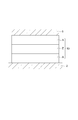
図1は本実施形態の凸版印刷版を模式的に示す図である。図1(A)は凸版印刷版の平面図であり、図1(B)はその断面図である。図1では、互いに所定の間隔をあけて、所定の方向に延在する複数本の凸部11、すなわちストライプ状に配置される複数本の凸部11が、可撓性支持膜100上に形成された凸版印刷版12を、実施の一形態として示している。なお図1(A)および後述する図2では窪み14にハッチングを施している。
FIG. 1 is a diagram schematically showing a relief printing plate of this embodiment. FIG. 1A is a plan view of a relief printing plate, and FIG. 1B is a cross-sectional view thereof. In FIG. 1, a plurality of protrusions 11 extending in a predetermined direction with a predetermined interval from each other, that is, a plurality of protrusions 11 arranged in a stripe shape are formed on the flexible support film 100. The made relief printing plate 12 is shown as one embodiment. In addition, in FIG. 1 (A) and FIG. 2 mentioned later, the hollow 14 is hatched.
図1に示すように凸版印刷版12の凸部11には所定の窪み14が設けられている。窪み14の形状およびその配置はインキの転写量に応じて適宜設定される。たとえば平面視において、凸部11の面積に占める窪み14の面積の割合や、窪み14の深さを適宜調整することによってインキの転写量を調整することができる。
As shown in FIG. 1, a predetermined depression 14 is provided in the convex portion 11 of the relief printing plate 12. The shape and arrangement of the recesses 14 are appropriately set according to the amount of ink transferred. For example, in plan view, the amount of ink transferred can be adjusted by appropriately adjusting the ratio of the area of the depressions 14 to the area of the protrusions 11 and the depth of the depressions 14.
前記凸部11は、点対称となるように配置された複数の前記窪み14を有することが好ましい。すなわち凸版印刷版12の厚み方向に垂直な平面上において、複数の前記窪み14は、点対称となるように配置されていることが好ましい。換言すると各凸部11において、凸版印刷版12の厚み方向にその軸線方向が一致する所定の対称軸に対して、線対称となるように窪み14が形成されていることが好ましい。なお後述するように凸版印刷版12は所定の版胴に巻き回されて使用されるが、上記窪み14の配置は、凸版印刷版12を平面上に載置した状態での配置を意味する。このように対称に複数の窪みを配置することによって、転写ロールから凸部に転写されるインキの膜厚を均一にすることができ、結果として均一な膜厚の薄膜を被印刷体に形成することができる。
It is preferable that the convex part 11 has a plurality of the depressions 14 arranged so as to be point-symmetric. In other words, on the plane perpendicular to the thickness direction of the relief printing plate 12, the plurality of depressions 14 are preferably arranged so as to be point-symmetric. In other words, it is preferable that the depressions 14 are formed in each convex portion 11 so as to be line symmetric with respect to a predetermined symmetry axis whose axial direction coincides with the thickness direction of the relief printing plate 12. As will be described later, the relief printing plate 12 is used by being wound around a predetermined plate cylinder. The arrangement of the depressions 14 means an arrangement in a state where the relief printing plate 12 is placed on a plane. By arranging a plurality of depressions symmetrically in this way, the film thickness of the ink transferred from the transfer roll to the convex portion can be made uniform, and as a result, a thin film with a uniform film thickness is formed on the printing medium. be able to.
図1では、各凸部の延在する方向に垂直な幅方向に2つの窪み14がそれぞれ設けられた凸版印刷版を示しているが、幅方向の窪みの数は2つに限らず、1つ、または3つ以上であってもよい。また図1では平面視で円形の窪み14を示しているが、窪み14の平面視の形状は円形に限らず多角形状でも、略楕円状であってもよい。なお幅方向は、基板の厚み方向に対しても垂直な方向である。
FIG. 1 shows a relief printing plate in which two depressions 14 are provided in the width direction perpendicular to the direction in which each protrusion extends, but the number of depressions in the width direction is not limited to two. It may be one, or three or more. In FIG. 1, the circular depression 14 is shown in plan view, but the shape of the depression 14 in plan view is not limited to a circle, and may be polygonal or substantially elliptical. The width direction is also a direction perpendicular to the thickness direction of the substrate.
また図1では窪みが離散的に設けられた凸部を示したが、窪みは連続して形成されていてもよい。図2は連続した窪みが形成された凸部を模式的に示す図である。図2では複数本形成される凸部のうちの1つの凸部を拡大して模式的に示している。なお窪みが連続して形成されている形態であっても、窪みは、点対称となるように配置されていることが好ましい。
Moreover, although the convex part in which the hollow was provided discretely was shown in FIG. 1, the hollow may be formed continuously. FIG. 2 is a diagram schematically showing a convex portion in which continuous depressions are formed. In FIG. 2, one convex part of the convex part formed in multiple numbers is expanded and shown typically. Even if the depressions are continuously formed, the depressions are preferably arranged so as to be point-symmetric.
たとえば互いに所定の間隔をあけて、所定の方向に延在する複数本の前記凸部を有する凸版印刷版の場合、すなわちストライプ状の凸部を有する凸版印刷版の場合、前記凸部11は、前記所定の方向に延在する複数本の前記窪み、または前記所定の方向に垂直な方向に延在する複数本の前記窪みを有することが好ましい。すなわち凸部は、図2(A)に示すように凸部の延在する方向と同じ方向に延在する窪み14、または図2(B)に示すように凸部の延在する方向とは垂直な方向に延在する窪み14を有することが好ましい。なお図2(A)では凸部の延在する方向と同じ方向に延在する3本の窪みが形成された凸部を示しているが、窪みの本数は3本に限らず、1本以上であればよい。
For example, in the case of a relief printing plate having a plurality of projections extending in a prescribed direction at a predetermined interval from each other, that is, in the case of a relief printing plate having stripe-like projections, the projection 11 is: It is preferable to have a plurality of the recesses extending in the predetermined direction or a plurality of the recesses extending in a direction perpendicular to the predetermined direction. That is, the convex portion is a recess 14 extending in the same direction as the direction in which the convex portion extends as shown in FIG. 2 (A), or the direction in which the convex portion extends as shown in FIG. 2 (B). It is preferable to have a recess 14 extending in the vertical direction. Note that FIG. 2A shows a convex portion in which three dents extending in the same direction as the direction in which the convex portion extends are shown, but the number of dents is not limited to three, but one or more. If it is.
また図2(C)に示すように、凸部11には格子状の窪み14が形成されていてもよく、また図2(D)に示すように、凸部11には平面視においてV字状の窪み14が形成されていてもよい。
Further, as shown in FIG. 2C, a lattice-like depression 14 may be formed in the convex portion 11, and as shown in FIG. 2D, the convex portion 11 has a V-shape in plan view. A dent 14 may be formed.
次に窪みが形成された凸部11を備える凸版印刷版12の作製方法について説明する。本実施形態の凸版印刷版12は例えば感光性樹脂を用いて作製することができる。たとえば、図5(A)に示すように、まず所定の基材100上にネガ型の感光性樹脂(フォトレジスト)11’を成膜する。ネガ型の感光性樹脂11’は露光されると現像液に対して溶解性が低下し、現像後に露光部分が残るという性質を有している。次にフォトマスクMを介して、UV光で感光性樹脂11’を露光し、凸部11を構成する部位を硬化させる。なお露光の際には、凸部11が形成される領域(a)から窪み14が形成される領域(b)(図5(B)参照)を除いた領域<領域(a)-領域(b)>と、領域(b)とで、露光量を異ならせる。なお、窪み14に対応する領域(b)のみを露光する場合を図5(B)に示す。露光量を異ならせる場合、具体的には領域(b)よりも領域<領域(a)-領域(b)>の露光量を多くする。露光量を異ならせるために、露光は2回に分けて行ってもよい。たとえば1回目は、図6に示すように、凸部形成予定領域において、領域(a-b)={領域(a)-領域(b)}を露光し、2回目は、領域(a)を露光すればよい。領域(b)は、領域(a)に含まれるものであるから、領域(b)の露光量が領域(a)の露光量よりも低くなる。もちろん、1回目の領域(a-b)の露光量が大きい場合には、2回目において、領域(b)のみを領域(a-b)の露光量(単位面積当たりの露光量)よりも小さな露光量(単位面積当たりの露光量)で露光してもよい。そして未硬化の感光性樹脂を洗い流し、現像する。上述したように露光量を異ならせることによって、領域(b)よりも領域<領域(a)-領域(b)>がより硬化しているため、現像の際には、領域(b)よりも領域<領域(a)-領域(b)>がより残存することになり、換言すれば、凸部形成予定領域において、領域(b)がその周辺よりも顕著に溶解することにより、窪み14が頂面に形成された凸部11が得られる。このようにして凸版印刷版12を得ることができる。なお露光は、感光性樹脂側のみから行ってもよいが、基材が露光光に対して透明である場合には、基材側からも予め露光していてもよい。
Next, a method for producing a relief printing plate 12 including the projections 11 with depressions will be described. The relief printing plate 12 of this embodiment can be produced using, for example, a photosensitive resin. For example, as shown in FIG. 5A, first, a negative photosensitive resin (photoresist) 11 ′ is formed on a predetermined substrate 100. The negative photosensitive resin 11 ′ has a property that when exposed to light, the solubility in the developer is lowered, and the exposed portion remains after development. Next, the photosensitive resin 11 ′ is exposed with UV light through the photomask M, and the portion constituting the convex portion 11 is cured. At the time of exposure, the region excluding the region (b) where the depressions 14 are formed from the region (a) where the convex portions 11 are formed (see FIG. 5B) <region (a) −region (b )> And the region (b), the exposure amount is varied. FIG. 5B shows a case where only the region (b) corresponding to the depression 14 is exposed. When different exposure amounts are used, specifically, the exposure amount of the region <region (a) −region (b)> is made larger than that of the region (b). In order to vary the exposure amount, the exposure may be performed in two steps. For example, as shown in FIG. 6, in the first time, the region (ab) = {region (a) −region (b)} is exposed in the projected portion formation region, and the second time, the region (a) is exposed. What is necessary is just to expose. Since the region (b) is included in the region (a), the exposure amount of the region (b) is lower than the exposure amount of the region (a). Of course, when the exposure amount of the first region (ab) is large, only the region (b) is smaller than the exposure amount (exposure amount per unit area) of the region (ab) in the second time. You may expose by exposure amount (exposure amount per unit area). Then, the uncured photosensitive resin is washed away and developed. As described above, the region <region (a) −region (b)> is hardened more than the region (b) by varying the exposure amount. Therefore, during development, the region <b> The region <region (a) -region (b)> remains, in other words, in the region where the projection is to be formed, the region (b) is significantly dissolved from the periphery thereof, so that the depression 14 is formed. The convex part 11 formed in the top surface is obtained. In this way, the relief printing plate 12 can be obtained. The exposure may be performed only from the photosensitive resin side. However, when the substrate is transparent to the exposure light, the exposure may be performed in advance from the substrate side.
感光性樹脂11’としてはたとえばポリアミド、ポリイミド、又はアクリレートなどを用いることができる。基材100にはポリエチレンテレフタレート、ポリイミド、又はポリカーボネイトなどを用いることができる。
As the photosensitive resin 11 ', for example, polyamide, polyimide, acrylate, or the like can be used. For the substrate 100, polyethylene terephthalate, polyimide, polycarbonate, or the like can be used.
次に上述した凸版印刷版12を用いて薄膜を製造する方法について説明する。図3は、上述した凸版印刷版12を備える印刷装置21を模式的に示す図である。印刷装置21は主に、インキ供給源22と、前記インキ供給源22からインキが供給される、表面が平坦な転写ロール23と、前記転写ロール23の表面に供給されたインキが転写される上述の凸版印刷版12とを備える。
Next, a method for producing a thin film using the above-described relief printing plate 12 will be described. FIG. 3 is a diagram schematically illustrating a printing apparatus 21 including the relief printing plate 12 described above. The printing apparatus 21 mainly includes an ink supply source 22, a transfer roll 23 having a flat surface to which ink is supplied from the ink supply source 22, and the ink supplied to the surface of the transfer roll 23. The relief printing plate 12 is provided.
上述したように凸版印刷版12は通常版胴24に巻き回されて使用される。たとえばストライプ状の凸部が設けられた凸版印刷版を使用する場合、凸版印刷版は、凸部の延在する方向が版胴の周方向に一致するように、または凸部の延在する方向が版胴の軸線方向に一致するように版胴に巻き回される。本実施形態では版胴24は、軸心CR1を中心に回転可能に軸支され、回転駆動機構DRV1からの駆動力によって回転する。図3では版胴24は矢印で示すように時計回りに回転し、この版胴24の回転にともなって凸版印刷版12も回転する。
As described above, the relief printing plate 12 is usually used by being wound around the plate cylinder 24. For example, when using a relief printing plate provided with stripe-shaped projections, the relief printing plate should be such that the direction in which the projections extend matches the circumferential direction of the plate cylinder, or the direction in which the projections extend. Is wound around the plate cylinder so as to coincide with the axial direction of the plate cylinder. In the present embodiment, the plate cylinder 24 is rotatably supported around the axis CR1 and is rotated by a driving force from the rotation driving mechanism DRV1. In FIG. 3, the plate cylinder 24 rotates clockwise as indicated by an arrow, and the relief printing plate 12 also rotates as the plate cylinder 24 rotates.
転写ロール23は、その軸心CR2が版胴24の軸心と平行になるように、回転可能に軸支され、回転駆動機構DRV2からの駆動力によって回転する。図3では矢印で示すように、転写ロール23は、反時計回りに回転する。転写ロール23はたとえばクロム、酸化クロム、アルミニウム、酸化アルミニウムなどによって構成される。
The transfer roll 23 is rotatably supported so that its axis CR2 is parallel to the axis of the plate cylinder 24, and rotates by the driving force from the rotation driving mechanism DRV2. In FIG. 3, as indicated by an arrow, the transfer roll 23 rotates counterclockwise. The transfer roll 23 is made of, for example, chromium, chromium oxide, aluminum, aluminum oxide, or the like.
インキ供給源22は、インキを収容し、さらにこれを転写ロール23に供給する。本実施形態ではスリットノズル25を用いて、転写ロール23にインキを供給する。
The ink supply source 22 stores ink and supplies it to the transfer roll 23. In this embodiment, the slit nozzle 25 is used to supply ink to the transfer roll 23.
さらに本実施形態では印刷装置は洗浄機構26をさらに備える。洗浄機構26は、転写ロール23から凸版印刷版12にインキが転写された後に、転写ロール23上に残存するインキを洗浄する。たとえば洗浄機構26は、ドクターブレードを備え、このドクターブレードを転写ロール23に押し当てることによって、転写ロール23上に残存するインキを掻き落とす。なお所定のリンス液を用いて転写ロール23を洗浄してもよい。
Furthermore, in this embodiment, the printing apparatus further includes a cleaning mechanism 26. The cleaning mechanism 26 cleans the ink remaining on the transfer roll 23 after the ink is transferred from the transfer roll 23 to the relief printing plate 12. For example, the cleaning mechanism 26 includes a doctor blade, and scrapes ink remaining on the transfer roll 23 by pressing the doctor blade against the transfer roll 23. The transfer roll 23 may be washed using a predetermined rinse liquid.
印刷装置21は被印刷体27を搬送する搬送テーブル28をさらに備える。この搬送テーブル28は被印刷体27を保持し、凸版印刷版12の接線速度と同じ速度で、凸版印刷版12の接線方向に平行移動する。搬送テーブル28は通常、水平移動する。この搬送テーブル28の移動にともなって被印刷体も平行移動する。
The printing apparatus 21 further includes a transport table 28 that transports the printing medium 27. The transport table 28 holds the printing material 27 and moves in parallel to the tangential direction of the relief printing plate 12 at the same speed as the tangential velocity of the relief printing plate 12. The transfer table 28 normally moves horizontally. As the transport table 28 moves, the printing medium also moves in parallel.
インキ供給源22から供給されるインキは、スリットノズル25を通って転写ロール23上に供給される。このようにスリットノズル25からインキが供給されつつ、転写ロール23が回転することにより、転写ロール23の表面上にインキの薄膜が形成される。なお、転写ロール23の表面は平坦(平滑)である。別の言い方をすれば、転写ロール23の表面の二乗平均粗さ(RMS)は、凹凸を有する凸版印刷版12の表面のRMSよりも著しく小さい。
The ink supplied from the ink supply source 22 is supplied onto the transfer roll 23 through the slit nozzle 25. Thus, the ink roll is rotated while the ink is supplied from the slit nozzle 25, whereby an ink thin film is formed on the surface of the transfer roll 23. Note that the surface of the transfer roll 23 is flat (smooth). In other words, the root mean square roughness (RMS) of the surface of the transfer roll 23 is significantly smaller than the RMS of the surface of the relief printing plate 12 having irregularities.
凸版印刷版12は転写ロール23に当接した状態で回転するため、転写ロール23に供給されたインキが、凸版印刷版12の凸部の表面に順次転写される。
Since the relief printing plate 12 rotates in contact with the transfer roll 23, the ink supplied to the transfer roll 23 is sequentially transferred onto the surface of the projection of the relief printing plate 12.
このようにインキが転写され、凸部にインキを保持する凸版印刷版12は、被印刷体27にも押圧された状態で回転する。被印刷体27は凸版印刷版12の回転とともに平行移動するため、被印刷体27には、凸版印刷版12の凸部に保持されたインキが順次印刷される。
In this way, the relief printing plate 12 to which the ink is transferred and holds the ink on the convex portion rotates while being pressed against the printing medium 27. Since the printing medium 27 moves in parallel with the rotation of the relief printing plate 12, the ink held on the convex portions of the relief printing plate 12 is sequentially printed on the printing medium 27.
なお凸版印刷版12に転写されずに転写ロール23に残存したインキは、洗浄機構26によって転写ロール23から除去される。
The ink remaining on the transfer roll 23 without being transferred to the relief printing plate 12 is removed from the transfer roll 23 by the cleaning mechanism 26.
以上の工程によって、表面が平坦な転写ロールにインキを供給する工程と、上述の凸版印刷版を前記転写ロールに押し当て、インキを前記凸版印刷版に転写する工程と、凸版印刷版を被印刷体に押し当て、前記インキを印刷する工程とが行われ、さらに前記インキを固化し、被印刷体上にインキの薄膜を形成する工程とを行うことにより被印刷体上に薄膜が形成される。
Through the above steps, the step of supplying ink to a transfer roll having a flat surface, the step of pressing the above-described relief printing plate against the transfer roll, transferring the ink to the relief printing plate, and printing the relief printing plate And a step of printing the ink on the body, and further solidifying the ink to form a thin film of ink on the substrate, thereby forming a thin film on the substrate .
インキの固化は、溶媒を除去することによって行うことができる。溶媒の除去はたとえば自然乾燥、加熱乾燥、真空乾燥などによって行われる。またインキが、光や熱を加えることによって硬化する材料を含む場合は、被印刷体にインキが印刷された後に、光を照射したり、熱を加えたりすることによってインキを固化してもよい。
The ink can be solidified by removing the solvent. The removal of the solvent is performed by, for example, natural drying, heat drying, vacuum drying, or the like. In addition, when the ink contains a material that is cured by applying light or heat, the ink may be solidified by irradiating light or applying heat after the ink is printed on the printing medium. .
上述したように、所定の窪み14を凸部11に形成することによって、意図した分量のインキを凸版印刷版12に転写することができる。これによって意図した分量のインキを被印刷体27に印刷することができ、結果として意図した膜厚の薄膜を、被印刷体上に形成することができる。
As described above, an intended amount of ink can be transferred to the relief printing plate 12 by forming the predetermined depressions 14 in the projections 11. As a result, an intended amount of ink can be printed on the printing medium 27, and as a result, a thin film having an intended thickness can be formed on the printing medium.
上述した印刷装置を用いることにより、被印刷体上に様々な種類の薄膜を形成することができる。たとえば用いるインキを適宜調整することによって、電極や配線として機能する導電性薄膜、有機光電変換素子の活性層、有機薄膜トランジスタの半導体層、および後述する有機EL素子の有機EL層などを形成することができる。
By using the printing apparatus described above, various types of thin films can be formed on the substrate. For example, by appropriately adjusting the ink to be used, a conductive thin film functioning as an electrode or a wiring, an active layer of an organic photoelectric conversion element, a semiconductor layer of an organic thin film transistor, and an organic EL layer of an organic EL element described later can be formed. it can.
上述した凸版印刷法を用いて、有機EL素子を形成することができる。すなわち本実施の形態の有機EL素子1の製造方法は、図7に示すように、一対の電極2,5と、該電極間に設けられる有機EL層10とを備える有機EL素子の製造方法であって、一対の電極のうちの一方の電極2を形成する工程と、表面が平坦な転写ロールに、有機EL層(特に発光層4)10となる材料を含む有機ELインキを供給する工程と、上述の凸版印刷版12を転写ロール23に押し当て、有機ELインキを凸版印刷版12に転写する工程と、凸版印刷版12を一対の前記一方の電極2に押し当て、有機ELインキを印刷する工程と、有機ELインキを固化し、一方の電極2上に有機EL層(特に発光層4)10を形成する工程と、前記有機EL層10上に一対の電極のうちの他方の電極5を形成する工程とを含む、有機EL素子の製造方法に関する。
An organic EL element can be formed using the above-described relief printing method. That is, the manufacturing method of the organic EL element 1 of the present embodiment is a manufacturing method of an organic EL element including a pair of electrodes 2 and 5 and an organic EL layer 10 provided between the electrodes as shown in FIG. A step of forming one electrode 2 of the pair of electrodes, and a step of supplying an organic EL ink containing a material to be the organic EL layer (particularly, the light emitting layer 4) 10 to a transfer roll having a flat surface. The above-described relief printing plate 12 is pressed against the transfer roll 23 to transfer the organic EL ink to the relief printing plate 12, and the relief printing plate 12 is pressed against the pair of one electrode 2 to print the organic EL ink. The step of solidifying the organic EL ink, forming the organic EL layer (particularly the light emitting layer 4) 10 on one electrode 2, and the other electrode 5 of the pair of electrodes on the organic EL layer 10 Forming an organic EL Child process for the preparation of.
有機EL素子1はたとえば表示装置の画素として用いられる。このような表示装置では、図15に示すように、支持基板6上に複数の有機EL素子1が所定の配列で整列して設けられる。たとえば複数の有機EL素子1は、支持基板6上においてマトリクス状に配置される。すなわち複数の有機EL素子1は、所定の行方向に所定の間隔をあけるとともに、所定の列方向に所定の間隔をあけて、整列して配置される。
The organic EL element 1 is used as a pixel of a display device, for example. In such a display device, as shown in FIG. 15, a plurality of organic EL elements 1 are arranged on a support substrate 6 in a predetermined arrangement. For example, the plurality of organic EL elements 1 are arranged in a matrix on the support substrate 6. That is, the plurality of organic EL elements 1 are arranged in a line with a predetermined interval in a predetermined row direction and with a predetermined interval in a predetermined column direction.
支持基板6上には通常複数の有機EL素子を区分けするための隔壁IWが設けられる。そして複数の有機EL素子は隔壁IWによって区分けされた領域にそれぞれ形成される。
A partition wall IW for separating a plurality of organic EL elements is usually provided on the support substrate 6. The plurality of organic EL elements are respectively formed in regions divided by the partition walls IW.
隔壁IWは、たとえばストライプ状、または格子状に設けられる。ストライプ状の隔壁が設けられる場合、所定の方向に延在する複数本の隔壁が、互いに所定の間隔をあけて基板上に設けられる。そして各有機EL素子1は、各隔壁IW間に設けられ、この隔壁IW間において、隔壁IWの延在する方向に沿って所定の間隔をあけて配置される。また格子状の隔壁IWが設けられる場合、各有機EL素子1は、それぞれ格子状の隔壁によって区分けされた領域にそれぞれ設けられる。
The partition wall IW is provided in a stripe shape or a lattice shape, for example. In the case where stripe-shaped partition walls are provided, a plurality of partition walls extending in a predetermined direction are provided on the substrate at predetermined intervals. And each organic EL element 1 is provided between each partition IW, and is arrange | positioned at predetermined intervals along the direction where the partition IW extends between these partition IW. Further, when the lattice-shaped partition wall IW is provided, each organic EL element 1 is provided in a region divided by the lattice-shaped partition wall.
本実施形態ではストライプ状の隔壁IWが設けられる基板に複数の有機EL素子を作製する方法について説明する。
In the present embodiment, a method for manufacturing a plurality of organic EL elements on a substrate provided with a stripe-shaped partition wall IW will be described.
有機EL素子1は一対の電極2,5を備える。一対の電極は、陽極と陰極とから構成される。すなわち一対の電極のうちの一方の電極は、陽極および陰極のうちのいずれか一方の電極として機能し、一対の電極のうちの他方の電極は、陽極および陰極のうちのいずれか他方の電極として機能する。まず支持基板6上に各有機EL素子の一方の電極2をそれぞれ形成する。すなわち有機EL素子1の数に対応する数の一方の電極2を支持基板6上に形成する。複数の一方の電極2は、平面視において、マトリクス状に配置される。
Organic EL element 1 includes a pair of electrodes 2 and 5. The pair of electrodes includes an anode and a cathode. That is, one of the pair of electrodes functions as one of the anode and the cathode, and the other of the pair of electrodes serves as the other of the anode and the cathode. Function. First, one electrode 2 of each organic EL element is formed on the support substrate 6. That is, one electrode 2 having a number corresponding to the number of organic EL elements 1 is formed on the support substrate 6. The plurality of one electrodes 2 are arranged in a matrix in a plan view.
次にストライプ状の隔壁IWを形成する。ストライプ状の隔壁は、隣り合う一方の電極2、2間に形成される。この隔壁IWはたとえば感光性樹脂を用いて、フォトリソグラフィ法によって形成することができる。
Next, a stripe-shaped partition wall IW is formed. A stripe-shaped partition is formed between one adjacent electrode 2 and 2. The partition wall IW can be formed by a photolithography method using, for example, a photosensitive resin.
つぎに有機EL層10を形成する。本実施形態では、ストライプ状の隔壁IW間に、有機EL層10となる材料を含む有機ELインキを供給し、さらにこれを固化することによって、ストライプ状の隔壁IW間に、帯状の有機EL層を形成する。なおストライプ状の隔壁IW間への有機ELインキの供給は、上述した凸版印刷法によって行われる。すなわち上述の凸版印刷法において、インキとして、有機EL層となる材料を含む有機ELインキを使用し、さらに、凸版印刷版12として、隔壁IW,IW間のパターンに対応するストライプ状の凸部11が形成された凸版印刷版12を使用する。上述した凸版印刷法によって隔壁IW,IW間に有機ELインキを供給し、さらにこれを固化することによって、帯状の有機EL層10を各隔壁IW,IW間に形成することができる。
Next, the organic EL layer 10 is formed. In the present embodiment, an organic EL ink containing a material to be the organic EL layer 10 is supplied between the stripe-shaped partition walls IW, and further solidified to thereby form a strip-shaped organic EL layer between the stripe-shaped partition walls IW. Form. The organic EL ink is supplied between the stripe-shaped partition walls IW by the above-described relief printing method. That is, in the above-described relief printing method, an organic EL ink containing a material that becomes an organic EL layer is used as the ink. Further, as the relief printing plate 12, stripe-like projections 11 corresponding to the pattern between the partition walls IW and IW are used. The letterpress printing plate 12 on which is formed is used. By supplying the organic EL ink between the partition walls IW and IW by the above-described relief printing method and further solidifying it, the strip-shaped organic EL layer 10 can be formed between the partition walls IW and IW.
有機EL層10を形成する際に用いられる有機ELインキは、その固形分濃度が通常0.5重量%~3重量%程度であり、その粘度が通常5cP~100cP程度である。1cP(センチポアズ)=0.001Pa・s(パスカル秒)であるから、5cP~100cPは、0.005Pa・s~0.1Pa・sである。有機ELインキの溶媒または分散媒は、有機EL層となる材料を均一に溶解または分散するものであればよい。たとえばクロロホルム、塩化メチレン、ジクロロエタンなどの塩素系溶媒、テトラヒドロフランなどのエーテル系溶媒、トルエン、キシレンなどの芳香族炭化水素系溶媒、アセトン、メチルエチルケトンなどのケトン系溶媒、酢酸エチル、酢酸ブチル、エチルセルソルブアセテートなどのエステル系溶媒、および水などを溶媒または分散媒として適宜使用することができる。
The organic EL ink used for forming the organic EL layer 10 has a solid content concentration of usually about 0.5 wt% to 3 wt% and a viscosity of usually about 5 cP to 100 cP. Since 1 cP (centipoise) = 0.001 Pa · s (Pascal second), 5 cP to 100 cP is 0.005 Pa · s to 0.1 Pa · s. The solvent or dispersion medium of the organic EL ink may be any solvent that uniformly dissolves or disperses the material that becomes the organic EL layer. For example, chlorinated solvents such as chloroform, methylene chloride, dichloroethane, ether solvents such as tetrahydrofuran, aromatic hydrocarbon solvents such as toluene and xylene, ketone solvents such as acetone and methyl ethyl ketone, ethyl acetate, butyl acetate, and ethyl cellosolve An ester solvent such as acetate and water can be appropriately used as a solvent or a dispersion medium.
有機EL層10の膜厚は通常30nm~120nm程度である。有機EL素子1の特性は有機EL層10の膜厚に大きく依存するため、意図した膜厚の有機EL層を形成することが望まれている。本実施形態では、凸版印刷版12の凸部11に所定の窪みを形成することによって、意図した分量の有機ELインキを隔壁IW,IW間に供給することができ、結果として、意図した膜厚の有機EL層10を形成することができる。これによって所期の特性を有する有機EL素子1を形成することができる。
The film thickness of the organic EL layer 10 is usually about 30 nm to 120 nm. Since the characteristics of the organic EL element 1 greatly depend on the film thickness of the organic EL layer 10, it is desired to form an organic EL layer having an intended film thickness. In the present embodiment, an intended amount of organic EL ink can be supplied between the partition walls IW and IW by forming a predetermined depression in the convex portion 11 of the relief printing plate 12, and as a result, the intended film thickness is obtained. The organic EL layer 10 can be formed. Thereby, the organic EL element 1 having desired characteristics can be formed.
一対の電極2,5間には、1層の有機EL層に限らず、複数の有機EL層が必要に応じて設けられる。なお有機EL層とは一対の電極間に設けられる全ての層を意味する。一対の電極間には少なくとも1層の発光層4が有機EL層として設けられる(図14参照)。複数の有機EL層が設けられる場合には、少なくとも1層の有機EL層が上述の本発明の凸版印刷法によって形成される。なお複数の有機EL層のうち、塗布法によって形成することが可能な有機EL層は、上述した本発明の凸版印刷法によって形成することが好ましい。なおカラー表示装置の場合には、赤色、緑色、青色をそれぞれ発光する有機ELインキを所定の隔壁IW,IW間に塗り分ける必要がある。この場合、各色の有機ELインキが供給されるパターンに対応するように、印刷版の凸部11のパターンを形成することによって、各色の有機ELインキを塗り分けることができる。
Between the pair of electrodes 2 and 5, not only one organic EL layer but also a plurality of organic EL layers are provided as necessary. The organic EL layer means all layers provided between a pair of electrodes. At least one light emitting layer 4 is provided as an organic EL layer between the pair of electrodes (see FIG. 14). When a plurality of organic EL layers are provided, at least one organic EL layer is formed by the relief printing method of the present invention described above. Of the plurality of organic EL layers, the organic EL layer that can be formed by a coating method is preferably formed by the relief printing method of the present invention described above. In the case of a color display device, it is necessary to coat organic EL inks that emit red, green, and blue light separately between predetermined partitions IW and IW. In this case, the organic EL ink of each color can be applied separately by forming the pattern of the convex portion 11 of the printing plate so as to correspond to the pattern to which the organic EL ink of each color is supplied.
有機EL層10を形成した後に、有機EL層上に他方の電極5を形成する。これによって、図15に示すように、複数の有機EL層10が基板6上に形成される。上述の電極の形成方法としては、真空蒸着法、スパッタ法、イオンプレーティング法、ラミネート法、或いはメッキ法を用いることができる。
After forming the organic EL layer 10, the other electrode 5 is formed on the organic EL layer. As a result, a plurality of organic EL layers 10 are formed on the substrate 6 as shown in FIG. As a method for forming the above-described electrode, a vacuum deposition method, a sputtering method, an ion plating method, a lamination method, or a plating method can be used.
なお本実施形態ではストライプ状の隔壁IWが形成される基板6上に複数の有機EL素子1を形成する方法について説明したが、格子状の隔壁が形成された基板上に複数の有機EL素子を形成する方法であっても、上述した凸版印刷法によって、各有機EL素子の有機EL層を形成することができる。この場合、格子状の隔壁によって区分けされるマトリクス状のパターンに対応するように、マトリクス状に配置される複数の凸部が形成された凸版印刷版を使用すればよい。
In the present embodiment, the method of forming the plurality of organic EL elements 1 on the substrate 6 on which the stripe-shaped partition walls IW are formed has been described. However, the plurality of organic EL elements are formed on the substrate on which the lattice-shaped partition walls are formed. Even if it is the method of forming, the organic EL layer of each organic EL element can be formed by the relief printing method mentioned above. In this case, a relief printing plate in which a plurality of projections arranged in a matrix form is used so as to correspond to the matrix pattern divided by the grid-like partition walls may be used.
<有機EL素子の構成>
有機EL素子は種々の層構成をとりうるが、以下では有機EL素子の層構造、各層の構成、および各層の形成方法についてさらに詳しく説明する。 <Configuration of organic EL element>
The organic EL element can have various layer configurations. The layer structure of the organic EL element, the configuration of each layer, and the method for forming each layer will be described in more detail below.
有機EL素子は、一対の電極2,5と、該電極2,5間に設けられる1または複数の有機EL層10とを含んで構成され、1または複数の有機EL層として少なくとも1層の発光層を有する。なお有機EL素子は、無機物と有機物とを含む層、および無機層などを含んでいてもよい。有機層を構成する有機物としては、低分子化合物でも高分子化合物でもよく、また低分子化合物と高分子化合物との混合物でもよい。有機層は、高分子化合物を含むことが好ましく、ポリスチレン換算の数平均分子量が103~108である高分子化合物を含むことが好ましい。
The organic EL element includes a pair of electrodes 2 and 5 and one or a plurality of organic EL layers 10 provided between the electrodes 2 and 5, and at least one layer of light emission as one or a plurality of organic EL layers. Has a layer. The organic EL element may include a layer containing an inorganic substance and an organic substance, an inorganic layer, and the like. The organic substance constituting the organic layer may be a low molecular compound or a high molecular compound, or a mixture of a low molecular compound and a high molecular compound. The organic layer preferably contains a polymer compound, and preferably contains a polymer compound having a polystyrene-equivalent number average molecular weight of 10 3 to 10 8 .
陰極と発光層との間に設けられる有機EL層としては、電子注入層、電子輸送層、正孔ブロック層などを挙げることができる。陰極と発光層との間に電子注入層と電子輸送層との両方の層が設けられる場合、陰極に近い層を電子注入層といい、発光層に近い層を電子輸送層という。陽極と発光層との間に設けられる有機EL層としては、正孔注入層、正孔輸送層、電子ブロック層などを挙げることができる。正孔注入層と正孔輸送層との両方の層が設けられる場合、陽極に近い層を正孔注入層といい、発光層に近い層を正孔輸送層という。
Examples of the organic EL layer provided between the cathode and the light emitting layer include an electron injection layer, an electron transport layer, and a hole blocking layer. When both the electron injection layer and the electron transport layer are provided between the cathode and the light emitting layer, the layer close to the cathode is called an electron injection layer, and the layer close to the light emitting layer is called an electron transport layer. Examples of the organic EL layer provided between the anode and the light emitting layer include a hole injection layer, a hole transport layer, and an electron block layer. When both the hole injection layer and the hole transport layer are provided, a layer close to the anode is referred to as a hole injection layer, and a layer close to the light emitting layer is referred to as a hole transport layer.
有機EL素子は前述したように一対の電極間に発光層以外にも所定の層を備えうる。支持基板6上に形成された電極(陽極)2と電極(陰極)5との間に形成される有機層10としては、以下の構造が挙げられる。
The organic EL element can include a predetermined layer in addition to the light emitting layer between the pair of electrodes as described above. Examples of the organic layer 10 formed between the electrode (anode) 2 and the electrode (cathode) 5 formed on the support substrate 6 include the following structures.
有機EL素子の構造としては、図7に示すように、電極(陽極)2と発光層4との間に有機層Yが介在すると共に、電極(陰極)5と発光層4との間に有機層Xが介在する構造とすることができる。
As shown in FIG. 7, the organic EL element has an organic layer Y between the electrode (anode) 2 and the light emitting layer 4 and an organic layer between the electrode (cathode) 5 and the light emitting layer 4. It can be set as the structure where the layer X interposes.
有機EL素子の構造としては、図8に示すように、電極(陽極)2と発光層4との間に有機層Yが介在し、発光層4上には直接的に電極5が形成されている構造とすることができる。
As shown in FIG. 8, the organic EL element has a structure in which an organic layer Y is interposed between the electrode (anode) 2 and the light emitting layer 4, and the electrode 5 is formed directly on the light emitting layer 4. It can be set as a structure.
有機EL素子の構造としては、図9に示すように、電極(陰極)5と発光層4との間に有機層Xが介在し、発光層4が直接的に電極2に接触している構造とすることができる。
As the structure of the organic EL element, as shown in FIG. 9, the organic layer X is interposed between the electrode (cathode) 5 and the light emitting layer 4, and the light emitting layer 4 is in direct contact with the electrode 2. It can be.
有機層Xは、図10に示すように、2種類以上の有機層X1,X2からなることとしてもよく、有機層Yは、図11に示すように、2種類以上の有機層Y1,Y2からなることとしてもよい。
The organic layer X may be composed of two or more kinds of organic layers X1 and X2 as shown in FIG. 10, and the organic layer Y is composed of two or more kinds of organic layers Y1 and Y2 as shown in FIG. It may be.
有機EL素子の構造としては、図14に示すように、陽極2と陰極5との間に発光層4のみが形成されていてもよい。
As the structure of the organic EL element, only the light emitting layer 4 may be formed between the anode 2 and the cathode 5 as shown in FIG.
陰極5と発光層4との間に設けられる層Xとしては、電子注入層、電子輸送層、正孔ブロック層などをあげることができる。図10に示したように、陰極5と発光層4との間に電子注入層X1と電子輸送層X2との両方の層が設けられる場合、陰極5に接する層を電子注入層X1といい、この電子注入層X1を除く層を電子輸送層X2という。
Examples of the layer X provided between the cathode 5 and the light emitting layer 4 include an electron injection layer, an electron transport layer, and a hole blocking layer. As shown in FIG. 10, when both the electron injection layer X1 and the electron transport layer X2 are provided between the cathode 5 and the light emitting layer 4, the layer in contact with the cathode 5 is referred to as the electron injection layer X1, The layer excluding the electron injection layer X1 is referred to as an electron transport layer X2.
電子注入層は、陰極からの電子注入効率を改善する機能を有する。電子輸送層は陰極側の表面に接する層からの電子注入を改善する機能を有する。正孔ブロック層は、正孔の輸送を堰き止める機能を有する。なお電子注入層、及び/又は電子輸送層が正孔の輸送を堰き止める機能を有する場合には、これらの層が正孔ブロック層を兼ねることがある。
The electron injection layer has a function of improving the electron injection efficiency from the cathode. The electron transport layer has a function of improving electron injection from the layer in contact with the surface on the cathode side. The hole blocking layer has a function of blocking hole transport. In the case where the electron injection layer and / or the electron transport layer have a function of blocking hole transport, these layers may also serve as the hole blocking layer.
正孔ブロック層が正孔の輸送を堰き止める機能を有することは、例えばホール電流のみを流す素子を作製し、その電流値の減少で堰き止める効果を確認することが可能である。
The fact that the hole blocking layer has a function of blocking hole transport makes it possible, for example, to produce an element that allows only hole current to flow, and confirm the blocking effect by reducing the current value.
陽極2と発光層4との間に設けられる層Yとしては、正孔注入層、正孔輸送層、電子ブロック層などをあげることができる。図11に示したように、陽極2と発光層4との間に、正孔注入層Y1と正孔輸送層Y2との両方の層が設けられる場合、陽極2に接する層を正孔注入層Y1といい、この正孔注入層Y1を除く層を正孔輸送層Y2という。
Examples of the layer Y provided between the anode 2 and the light emitting layer 4 include a hole injection layer, a hole transport layer, and an electron block layer. As shown in FIG. 11, when both the hole injection layer Y1 and the hole transport layer Y2 are provided between the anode 2 and the light emitting layer 4, the layer in contact with the anode 2 is the hole injection layer. The layer excluding the hole injection layer Y1 is referred to as Y1, and is referred to as a hole transport layer Y2.
正孔注入層は、陽極からの正孔注入効率を改善する機能を有する。正孔輸送層は陽極側の表面に接する層からの正孔注入を改善する機能を有する。電子ブロック層は、電子の輸送を堰き止める機能を有する。なお正孔注入層、及び/又は正孔輸送層が電子の輸送を堰き止める機能を有する場合には、これらの層が電子ブロック層を兼ねることがある。
The hole injection layer has a function of improving the hole injection efficiency from the anode. The hole transport layer has a function of improving hole injection from a layer in contact with the surface on the anode side. The electron blocking layer has a function of blocking electron transport. In the case where the hole injection layer and / or the hole transport layer has a function of blocking electron transport, these layers may also serve as an electron blocking layer.
電子ブロック層が電子の輸送を堰き止める機能を有することは、例えば、電子電流のみを流す素子を作製し、その電流値の減少で堰き止める効果を確認することが可能である。
The fact that the electron blocking layer has a function of blocking electron transport makes it possible, for example, to produce an element that allows only electron current to flow, and confirm the blocking effect by reducing the current value.
なお、電子注入層および正孔注入層を総称して電荷注入層ということがあり、電子輸送層および正孔輸送層を総称して電荷輸送層ということがある。
本実施の形態の有機EL素子のとりうる層構成の一例を以下に示す。
a)陽極2/発光層4/陰極5(図14参照)
b)陽極2/正孔注入層Y/発光層4/陰極5(図8参照)
c)陽極2/正孔注入層Y/発光層4/電子注入層X/陰極5(図7参照)
d)陽極2/正孔注入層Y/発光層4/電子輸送層X/陰極5(図7参照)
e)陽極2/正孔注入層Y/発光層4/電子輸送層X2/電子注入層X1/陰極5(図7及び図10参照)
f)陽極2/正孔輸送層Y/発光層4/陰極5(図8参照)
g)陽極2/正孔輸送層Y/発光層4/電子注入層X/陰極5(図7参照)
h)陽極2/正孔輸送層Y/発光層4/電子輸送層X/陰極5(図7参照)
i)陽極2/正孔輸送層Y/発光層4/電子輸送層X2/電子注入層X1/陰極5(図7及び図10参照)
j)陽極2/正孔注入層Y1/正孔輸送層Y2/発光層4/陰極5(図8及び図11参照)
k)陽極2/正孔注入層Y1/正孔輸送層Y2/発光層4/電子注入層X/陰極5(図7及び図11参照)
l)陽極2/正孔注入層Y1/正孔輸送層Y2/発光層4/電子輸送層X/陰極5(図7及び図11参照)
m)陽極2/正孔注入層Y1/正孔輸送層Y2/発光層4/電子輸送層X2/電子注入層X1/陰極5(図7、図10及び図11参照)
n)陽極2/発光層4/電子注入層X/陰極5(図9参照)
o)陽極2/発光層4/電子輸送層X/陰極5(図9参照)
p)陽極2/発光層4/電子輸送層X2/電子注入層X1/陰極5(図9及び図10参照)
(ここで、記号「/」は、記号「/」を挟む各層が隣接して積層されていることを示す。以下同じ。)
本実施の形態の有機EL素子は2層以上の発光層を有していてもよい。上記a)~p)の層構成のうちのいずれか1つにおいて、陽極と陰極とに挟持された積層体を「構造単位A」とすると、2層の発光層を有する有機EL素子の構成として、下記q)に示す層構成を挙げることができる。なお2つある(構造単位A)の層構成は互いに同じでも、異なっていてもよい。
q)陽極2/(構造単位A)/電荷発生層Z/(構造単位A)/陰極5(図12参照)
また「(構造単位A)/電荷発生層Z」を「構造単位B」とすると、3層以上の発光層を有する有機EL素子の構成として、下記r)に示す層構成を挙げることができる。
r)陽極2/(構造単位B)x/(構造単位A)/陰極5(図13参照)
なお記号「x」は、2以上の整数を表し、(構造単位B)xは、構造単位Bがx段積層された積層体を表す。また複数ある(構造単位B)の層構成は同じでも、異なっていてもよい。 The electron injection layer and the hole injection layer are sometimes collectively referred to as a charge injection layer, and the electron transport layer and the hole transport layer are sometimes collectively referred to as a charge transport layer.
An example of a layer structure that can be taken by the organic EL element of the present embodiment is shown below.
a)Anode 2 / light emitting layer 4 / cathode 5 (see FIG. 14)
b)Anode 2 / hole injection layer Y / light emitting layer 4 / cathode 5 (see FIG. 8)
c)Anode 2 / hole injection layer Y / light emitting layer 4 / electron injection layer X / cathode 5 (see FIG. 7)
d)Anode 2 / hole injection layer Y / light emitting layer 4 / electron transport layer X / cathode 5 (see FIG. 7)
e)Anode 2 / hole injection layer Y / light emitting layer 4 / electron transport layer X2 / electron injection layer X1 / cathode 5 (see FIGS. 7 and 10)
f)Anode 2 / hole transport layer Y / light emitting layer 4 / cathode 5 (see FIG. 8)
g)Anode 2 / hole transport layer Y / light emitting layer 4 / electron injection layer X / cathode 5 (see FIG. 7)
h)Anode 2 / hole transport layer Y / light emitting layer 4 / electron transport layer X / cathode 5 (see FIG. 7)
i)Anode 2 / hole transport layer Y / light emitting layer 4 / electron transport layer X2 / electron injection layer X1 / cathode 5 (see FIGS. 7 and 10)
j)Anode 2 / hole injection layer Y1 / hole transport layer Y2 / light emitting layer 4 / cathode 5 (see FIGS. 8 and 11)
k)Anode 2 / hole injection layer Y1 / hole transport layer Y2 / light emitting layer 4 / electron injection layer X / cathode 5 (see FIGS. 7 and 11)
l)Anode 2 / hole injection layer Y1 / hole transport layer Y2 / light emitting layer 4 / electron transport layer X / cathode 5 (see FIGS. 7 and 11)
m)Anode 2 / hole injection layer Y1 / hole transport layer Y2 / light emitting layer 4 / electron transport layer X2 / electron injection layer X1 / cathode 5 (see FIGS. 7, 10 and 11)
n)Anode 2 / light emitting layer 4 / electron injection layer X / cathode 5 (see FIG. 9)
o)Anode 2 / light emitting layer 4 / electron transport layer X / cathode 5 (see FIG. 9)
p)Anode 2 / light emitting layer 4 / electron transport layer X2 / electron injection layer X1 / cathode 5 (see FIGS. 9 and 10)
(Here, the symbol “/” indicates that the layers sandwiching the symbol “/” are adjacently stacked. The same applies hereinafter.)
The organic EL element of the present embodiment may have two or more light emitting layers. In any one of the layer configurations of a) to p) above, when the laminate sandwiched between the anode and the cathode is referred to as “structural unit A”, the configuration of the organic EL device having two light emitting layers is as follows. And the layer structure shown in the following q). Note that the two (structural unit A) layer structures may be the same or different.
q)Anode 2 / (structural unit A) / charge generation layer Z / (structural unit A) / cathode 5 (see FIG. 12)
Further, when “(structural unit A) / charge generation layer Z” is “structural unit B”, examples of the configuration of the organic EL element having three or more light emitting layers include the layer configuration shown in the following r).
r)Anode 2 / (structural unit B) x / (structural unit A) / cathode 5 (see FIG. 13)
The symbol “x” represents an integer of 2 or more, and (structural unit B) x represents a stacked body in which the structural unit B is stacked in x stages. A plurality of (structural units B) may have the same or different layer structure.
本実施の形態の有機EL素子のとりうる層構成の一例を以下に示す。
a)陽極2/発光層4/陰極5(図14参照)
b)陽極2/正孔注入層Y/発光層4/陰極5(図8参照)
c)陽極2/正孔注入層Y/発光層4/電子注入層X/陰極5(図7参照)
d)陽極2/正孔注入層Y/発光層4/電子輸送層X/陰極5(図7参照)
e)陽極2/正孔注入層Y/発光層4/電子輸送層X2/電子注入層X1/陰極5(図7及び図10参照)
f)陽極2/正孔輸送層Y/発光層4/陰極5(図8参照)
g)陽極2/正孔輸送層Y/発光層4/電子注入層X/陰極5(図7参照)
h)陽極2/正孔輸送層Y/発光層4/電子輸送層X/陰極5(図7参照)
i)陽極2/正孔輸送層Y/発光層4/電子輸送層X2/電子注入層X1/陰極5(図7及び図10参照)
j)陽極2/正孔注入層Y1/正孔輸送層Y2/発光層4/陰極5(図8及び図11参照)
k)陽極2/正孔注入層Y1/正孔輸送層Y2/発光層4/電子注入層X/陰極5(図7及び図11参照)
l)陽極2/正孔注入層Y1/正孔輸送層Y2/発光層4/電子輸送層X/陰極5(図7及び図11参照)
m)陽極2/正孔注入層Y1/正孔輸送層Y2/発光層4/電子輸送層X2/電子注入層X1/陰極5(図7、図10及び図11参照)
n)陽極2/発光層4/電子注入層X/陰極5(図9参照)
o)陽極2/発光層4/電子輸送層X/陰極5(図9参照)
p)陽極2/発光層4/電子輸送層X2/電子注入層X1/陰極5(図9及び図10参照)
(ここで、記号「/」は、記号「/」を挟む各層が隣接して積層されていることを示す。以下同じ。)
本実施の形態の有機EL素子は2層以上の発光層を有していてもよい。上記a)~p)の層構成のうちのいずれか1つにおいて、陽極と陰極とに挟持された積層体を「構造単位A」とすると、2層の発光層を有する有機EL素子の構成として、下記q)に示す層構成を挙げることができる。なお2つある(構造単位A)の層構成は互いに同じでも、異なっていてもよい。
q)陽極2/(構造単位A)/電荷発生層Z/(構造単位A)/陰極5(図12参照)
また「(構造単位A)/電荷発生層Z」を「構造単位B」とすると、3層以上の発光層を有する有機EL素子の構成として、下記r)に示す層構成を挙げることができる。
r)陽極2/(構造単位B)x/(構造単位A)/陰極5(図13参照)
なお記号「x」は、2以上の整数を表し、(構造単位B)xは、構造単位Bがx段積層された積層体を表す。また複数ある(構造単位B)の層構成は同じでも、異なっていてもよい。 The electron injection layer and the hole injection layer are sometimes collectively referred to as a charge injection layer, and the electron transport layer and the hole transport layer are sometimes collectively referred to as a charge transport layer.
An example of a layer structure that can be taken by the organic EL element of the present embodiment is shown below.
a)
b)
c)
d)
e)
f)
g)
h)
i)
j)
k)
l)
m)
n)
o)
p)
(Here, the symbol “/” indicates that the layers sandwiching the symbol “/” are adjacently stacked. The same applies hereinafter.)
The organic EL element of the present embodiment may have two or more light emitting layers. In any one of the layer configurations of a) to p) above, when the laminate sandwiched between the anode and the cathode is referred to as “structural unit A”, the configuration of the organic EL device having two light emitting layers is as follows. And the layer structure shown in the following q). Note that the two (structural unit A) layer structures may be the same or different.
q)
Further, when “(structural unit A) / charge generation layer Z” is “structural unit B”, examples of the configuration of the organic EL element having three or more light emitting layers include the layer configuration shown in the following r).
r)
The symbol “x” represents an integer of 2 or more, and (structural unit B) x represents a stacked body in which the structural unit B is stacked in x stages. A plurality of (structural units B) may have the same or different layer structure.
ここで、電荷発生層Zとは電界を印加することにより正孔と電子を発生する層である。電荷発生層Zとしては、たとえば酸化バナジウム、インジウムスズ酸化物(Indium Tin Oxide:略称ITO)、酸化モリブデンなどから成る薄膜を挙げることができる。
Here, the charge generation layer Z is a layer that generates holes and electrons by applying an electric field. Examples of the charge generation layer Z include a thin film made of vanadium oxide, indium tin oxide (IndiumInTin Oxide: abbreviated as ITO), molybdenum oxide, or the like.
有機EL素子は通常支持基板上に設けられる。有機EL素子は、陽極および陰極から構成される一対の電極のうちの陽極を陰極よりも支持基板寄りに配して支持基板に設けてもよく、また陰極を陽極よりも支持基板寄りに配して支持基板に設けてもよい。たとえば上記a)~r)の構成において、右側から順に支持基板上に各層を積層した構成の有機EL素子でも、左側から順に支持基板上に各層を積層した構成の有機EL素子であってもよい。
Organic EL element is usually provided on a support substrate. The organic EL element may be provided on the support substrate with the anode of the pair of electrodes including the anode and the cathode disposed closer to the support substrate than the cathode, and the cathode is disposed closer to the support substrate than the anode. May be provided on the support substrate. For example, in the above-described configurations a) to r), an organic EL element having a structure in which each layer is stacked on the support substrate in order from the right side or an organic EL element having a structure in which each layer is stacked on the support substrate from the left side may be used. .
積層する層の順序、層数、および各層の厚さについては、発光効率や素子寿命を勘案して適宜設定することができる。
The order of the layers to be laminated, the number of layers, and the thickness of each layer can be appropriately set in consideration of light emission efficiency and element lifetime.
次に有機EL素子を構成する各層の材料および形成方法についてより具体的に説明する。
Next, the material and forming method of each layer constituting the organic EL element will be described more specifically.
<陽極>
発光層から放たれる光が陽極を通って素子外に出射する構成の有機EL素子の場合、陽極には光透過性を示す電極が用いられる。光透過性を示す電極としては、金属酸化物、金属硫化物および金属などの薄膜を用いることができ、電気伝導度および光透過率の高いものが好適に用いられる。具体的には酸化インジウム、酸化亜鉛、酸化スズ、ITO、インジウム亜鉛酸化物(Indium Zinc Oxide:略称IZO)、金、白金、銀、および銅などから成る薄膜が用いられ、これらの中でもITO、IZO、または酸化スズから成る薄膜が好適に用いられる。陽極の作製方法としては、真空蒸着法、スパッタリング法、イオンプレーティング法、メッキ法などを挙げることができる。また、該陽極として、ポリアニリンもしくはその誘導体、ポリチオフェンもしくはその誘導体などの有機の透明導電膜を用いてもよい。 <Anode>
In the case of an organic EL element having a configuration in which light emitted from the light emitting layer is emitted outside the element through the anode, an electrode exhibiting optical transparency is used for the anode. As the electrode exhibiting light transmittance, a thin film of metal oxide, metal sulfide, metal or the like can be used, and an electrode having high electrical conductivity and light transmittance is preferably used. Specifically, a thin film made of indium oxide, zinc oxide, tin oxide, ITO, indium zinc oxide (abbreviated as IZO), gold, platinum, silver, copper, or the like is used. Among these, ITO, IZO Or a thin film made of tin oxide is preferably used. Examples of a method for producing the anode include a vacuum deposition method, a sputtering method, an ion plating method, and a plating method. Further, an organic transparent conductive film such as polyaniline or a derivative thereof, polythiophene or a derivative thereof may be used as the anode.
陽極の膜厚は、求められる特性や成膜工程の簡易さなどを考慮して適宜設定され、例えば10nm~10μmであり、好ましくは20nm~1μmであり、さらに好ましくは50nm~500nmである。
The film thickness of the anode is appropriately set in consideration of the required characteristics and the simplicity of the film forming process, and is, for example, 10 nm to 10 μm, preferably 20 nm to 1 μm, and more preferably 50 nm to 500 nm.
<正孔注入層>
正孔注入層を構成する正孔注入材料としては、酸化バナジウム、酸化モリブデン、酸化ルテニウム、および酸化アルミニウムなどの酸化物や、フェニルアミン系、スターバースト型アミン系、フタロシアニン系、アモルファスカーボン、ポリアニリン、およびポリチオフェン誘導体などを挙げることができる。 <Hole injection layer>
As the hole injection material constituting the hole injection layer, oxides such as vanadium oxide, molybdenum oxide, ruthenium oxide, and aluminum oxide, phenylamine type, starburst type amine type, phthalocyanine type, amorphous carbon, polyaniline, And polythiophene derivatives.
正孔注入層の成膜方法としては、正孔注入材料を含む溶液からの成膜を挙げることができる。例えば正孔注入材料を含む溶液を所定の塗布法によって塗布成膜し、さらにこれを固化することによって正孔注入層を形成することができる。
Examples of the method for forming the hole injection layer include film formation from a solution containing a hole injection material. For example, a hole injection layer can be formed by coating a film containing a hole injection material by a predetermined coating method and solidifying the solution.
塗布法としてはスピンコート法、キャスティング法、マイクログラビアコート法、グラビアコート法、バーコート法、ロールコート法、ワイアーバーコート法、ディップコート法、スプレーコート法、スクリーン印刷法、凸版印刷法(フレキソ印刷法)、オフセット印刷法、インクジェットプリント法などを挙げることができ、実施の一形態として前述した本発明の凸版印刷法が好ましい。
As the coating method, spin coating method, casting method, micro gravure coating method, gravure coating method, bar coating method, roll coating method, wire bar coating method, dip coating method, spray coating method, screen printing method, letterpress printing method (flexographic printing method) Printing method), offset printing method, inkjet printing method and the like, and the relief printing method of the present invention described above as one embodiment is preferable.
正孔注入層の膜厚は、求められる特性および成膜工程の簡易さなどを考慮して適宜設定され、例えば1nm~1μmであり、好ましくは2nm~500nmであり、さらに好ましくは5nm~200nmである。
The film thickness of the hole injection layer is appropriately set in consideration of the required characteristics and the simplicity of the film forming process, and is, for example, 1 nm to 1 μm, preferably 2 nm to 500 nm, more preferably 5 nm to 200 nm. is there.
<正孔輸送層>
正孔輸送層を構成する正孔輸送材料としては、ポリビニルカルバゾール若しくはその誘導体、ポリシラン若しくはその誘導体、側鎖若しくは主鎖に芳香族アミンを有するポリシロキサン誘導体、ピラゾリン誘導体、アリールアミン誘導体、スチルベン誘導体、トリフェニルジアミン誘導体、ポリアニリン若しくはその誘導体、ポリチオフェン若しくはその誘導体、ポリアリールアミン若しくはその誘導体、ポリピロール若しくはその誘導体、ポリ(p-フェニレンビニレン)若しくはその誘導体、又はポリ(2,5-チエニレンビニレン)若しくはその誘導体などを挙げることができる。 <Hole transport layer>
As the hole transport material constituting the hole transport layer, polyvinylcarbazole or a derivative thereof, polysilane or a derivative thereof, a polysiloxane derivative having an aromatic amine in a side chain or a main chain, a pyrazoline derivative, an arylamine derivative, a stilbene derivative, Triphenyldiamine derivative, polyaniline or derivative thereof, polythiophene or derivative thereof, polyarylamine or derivative thereof, polypyrrole or derivative thereof, poly (p-phenylene vinylene) or derivative thereof, or poly (2,5-thienylene vinylene) or Examples thereof include derivatives thereof.
これらの中で正孔輸送材料としては、ポリビニルカルバゾール若しくはその誘導体、ポリシラン若しくはその誘導体、側鎖若しくは主鎖に芳香族アミン化合物基を有するポリシロキサン誘導体、ポリアニリン若しくはその誘導体、ポリチオフェン若しくはその誘導体、ポリアリールアミン若しくはその誘導体、ポリ(p-フェニレンビニレン)若しくはその誘導体、又はポリ(2,5-チエニレンビニレン)若しくはその誘導体などの高分子正孔輸送材料が好ましく、さらに好ましくはポリビニルカルバゾール若しくはその誘導体、ポリシラン若しくはその誘導体、側鎖若しくは主鎖に芳香族アミンを有するポリシロキサン誘導体である。低分子の正孔輸送材料の場合には、高分子バインダーに分散させて用いることが好ましい。
Among these, hole transport materials include polyvinyl carbazole or derivatives thereof, polysilane or derivatives thereof, polysiloxane derivatives having aromatic amine compound groups in the side chain or main chain, polyaniline or derivatives thereof, polythiophene or derivatives thereof, poly Preferred is a polymeric hole transport material such as arylamine or a derivative thereof, poly (p-phenylene vinylene) or a derivative thereof, or poly (2,5-thienylene vinylene) or a derivative thereof, more preferably polyvinyl carbazole or a derivative thereof. , Polysilane or a derivative thereof, and a polysiloxane derivative having an aromatic amine in the side chain or main chain. In the case of a low-molecular hole transport material, it is preferably used by being dispersed in a polymer binder.
正孔輸送層の成膜方法としては、特に制限はないが、低分子の正孔輸送材料では、高分子バインダーと正孔輸送材料とを含む混合液からの成膜を挙げることができ、高分子の正孔輸送材料では、正孔輸送材料を含む溶液からの成膜を挙げることができる。
The method for forming the hole transport layer is not particularly limited, but in the case of a low molecular hole transport material, film formation from a mixed solution containing a polymer binder and a hole transport material can be exemplified. Examples of molecular hole transport materials include film formation from a solution containing a hole transport material.
溶液からの成膜方法としては、前述した正孔注入層の成膜法と同様の塗布法を挙げることができる。
As a film formation method from a solution, the same coating method as the above-described film formation method of the hole injection layer can be exemplified.
混合する高分子バインダーとしては、電荷輸送を極度に阻害しないものが好ましく、また可視光に対する吸収の弱いものが好適に用いられ、例えばポリカーボネート、ポリアクリレート、ポリメチルアクリレート、ポリメチルメタクリレート、ポリスチレン、ポリ塩化ビニル、ポリシロキサンなどを挙げることができる。
As the polymer binder to be mixed, those that do not extremely inhibit charge transport are preferable, and those that weakly absorb visible light are preferably used. For example, polycarbonate, polyacrylate, polymethyl acrylate, polymethyl methacrylate, polystyrene, poly Examples thereof include vinyl chloride and polysiloxane.
正孔輸送層の膜厚は、求められる特性および成膜工程の簡易さなどを考慮して設定され、例えば1nm~1μmであり、好ましくは2nm~500nmであり、さらに好ましくは5nm~200nmである。
The film thickness of the hole transport layer is set in consideration of the required characteristics and the simplicity of the film forming process, and is, for example, 1 nm to 1 μm, preferably 2 nm to 500 nm, more preferably 5 nm to 200 nm. .
<発光層>
発光層は、通常、主として蛍光及び/又はりん光を発光する有機物、または該有機物とこれを補助するドーパントとから形成される。ドーパントは、例えば発光効率の向上や、発光波長を変化させるために加えられる。なお発光層を構成する有機物は、低分子化合物でも高分子化合物でもよく、塗布法によって発光層を形成する場合には、発光層は高分子化合物を含むことが好ましい。発光層を構成する高分子化合物のポリスチレン換算の数平均分子量はたとえば103~108程度である。発光層を構成する発光材料としては、例えば以下の色素系材料、金属錯体系材料、高分子系材料、ドーパント材料を挙げることができる。 <Light emitting layer>
The light emitting layer is usually formed of an organic substance that mainly emits fluorescence and / or phosphorescence, or an organic substance and a dopant that assists the organic substance. The dopant is added, for example, in order to improve the luminous efficiency and change the emission wavelength. In addition, the organic substance which comprises a light emitting layer may be a low molecular compound or a high molecular compound, and when forming a light emitting layer by the apply | coating method, it is preferable that a light emitting layer contains a high molecular compound. The number average molecular weight in terms of polystyrene of the polymer compound constituting the light emitting layer is, for example, about 10 3 to 10 8 . Examples of the light emitting material constituting the light emitting layer include the following dye materials, metal complex materials, polymer materials, and dopant materials.
(色素系材料)
色素系材料としては、例えば、シクロペンダミン誘導体、テトラフェニルブタジエン誘導体化合物、トリフェニルアミン誘導体、オキサジアゾール誘導体、ピラゾロキノリン誘導体、ジスチリルベンゼン誘導体、ジスチリルアリーレン誘導体、ピロール誘導体、チオフェン環化合物、ピリジン環化合物、ペリノン誘導体、ペリレン誘導体、オリゴチオフェン誘導体、オキサジアゾールダイマー、ピラゾリンダイマー、キナクリドン誘導体、クマリン誘導体などを挙げることができる。 (Dye material)
Examples of dye-based materials include cyclopentamine derivatives, tetraphenylbutadiene derivative compounds, triphenylamine derivatives, oxadiazole derivatives, pyrazoloquinoline derivatives, distyrylbenzene derivatives, distyrylarylene derivatives, pyrrole derivatives, thiophene ring compounds. Pyridine ring compounds, perinone derivatives, perylene derivatives, oligothiophene derivatives, oxadiazole dimers, pyrazoline dimers, quinacridone derivatives, coumarin derivatives, and the like.
(金属錯体系材料)
金属錯体系材料としては、例えばTb、Eu、Dyなどの希土類金属、またはAl、Zn、Be、Ir、Ptなどを中心金属に有し、オキサジアゾール、チアジアゾール、フェニルピリジン、フェニルベンゾイミダゾール、キノリン構造などを配位子に有する金属錯体を挙げることができ、例えばイリジウム錯体、白金錯体などの三重項励起状態からの発光を有する金属錯体、アルミニウムキノリノール錯体、ベンゾキノリノールベリリウム錯体、ベンゾオキサゾリル亜鉛錯体、ベンゾチアゾール亜鉛錯体、アゾメチル亜鉛錯体、ポルフィリン亜鉛錯体、フェナントロリンユーロピウム錯体などを挙げることができる。 (Metal complex materials)
Examples of metal complex materials include rare earth metals such as Tb, Eu, and Dy, or Al, Zn, Be, Ir, Pt, etc. as a central metal, and oxadiazole, thiadiazole, phenylpyridine, phenylbenzimidazole, quinoline. Examples include metal complexes having a structure as a ligand, for example, iridium complexes, platinum complexes and other metal complexes having light emission from a triplet excited state, aluminum quinolinol complexes, benzoquinolinol beryllium complexes, benzoxazolyl zinc A complex, a benzothiazole zinc complex, an azomethylzinc complex, a porphyrin zinc complex, a phenanthroline europium complex, and the like can be given.
(高分子系材料)
高分子系材料としては、ポリパラフェニレンビニレン誘導体、ポリチオフェン誘導体、ポリパラフェニレン誘導体、ポリシラン誘導体、ポリアセチレン誘導体、ポリフルオレン誘導体、ポリビニルカルバゾール誘導体、上記色素系材料や金属錯体系発光材料を高分子化したものなどを挙げることができる。 (Polymer material)
As polymer materials, polyparaphenylene vinylene derivatives, polythiophene derivatives, polyparaphenylene derivatives, polysilane derivatives, polyacetylene derivatives, polyfluorene derivatives, polyvinylcarbazole derivatives, the above dye materials and metal complex light emitting materials are polymerized. The thing etc. can be mentioned.
上記発光性材料のうち、青色に発光する材料としては、ジスチリルアリーレン誘導体、オキサジアゾール誘導体、およびそれらの重合体、ポリビニルカルバゾール誘導体、ポリパラフェニレン誘導体、ポリフルオレン誘導体などを挙げることができる。なかでも高分子材料のポリビニルカルバゾール誘導体、ポリパラフェニレン誘導体やポリフルオレン誘導体などが好ましい。
Among the luminescent materials described above, materials that emit blue light include distyrylarylene derivatives, oxadiazole derivatives, and polymers thereof, polyvinylcarbazole derivatives, polyparaphenylene derivatives, polyfluorene derivatives, and the like. Of these, polymer materials such as polyvinyl carbazole derivatives, polyparaphenylene derivatives, and polyfluorene derivatives are preferred.
また、緑色に発光する材料としては、キナクリドン誘導体、クマリン誘導体、およびそれらの重合体、ポリパラフェニレンビニレン誘導体、ポリフルオレン誘導体などを挙げることができる。なかでも高分子材料のポリパラフェニレンビニレン誘導体、ポリフルオレン誘導体などが好ましい。
In addition, examples of materials that emit green light include quinacridone derivatives, coumarin derivatives, and polymers thereof, polyparaphenylene vinylene derivatives, polyfluorene derivatives, and the like. Of these, polymer materials such as polyparaphenylene vinylene derivatives and polyfluorene derivatives are preferred.
また、赤色に発光する材料としては、クマリン誘導体、チオフェン環化合物、およびそれらの重合体、ポリパラフェニレンビニレン誘導体、ポリチオフェン誘導体、ポリフルオレン誘導体などを挙げることができる。なかでも高分子材料のポリパラフェニレンビニレン誘導体、ポリチオフェン誘導体、ポリフルオレン誘導体などが好ましい。
(ドーパント材料)
ドーパント材料としては、例えばペリレン誘導体、クマリン誘導体、ルブレン誘導体、キナクリドン誘導体、スクアリリウム誘導体、ポルフィリン誘導体、スチリル系色素、テトラセン誘導体、ピラゾロン誘導体、デカシクレン、フェノキサゾンなどを挙げることができる。なお、このような発光層の厚さは、通常約2nm~200nmである。 Examples of materials that emit red light include coumarin derivatives, thiophene ring compounds, and polymers thereof, polyparaphenylene vinylene derivatives, polythiophene derivatives, and polyfluorene derivatives. Among these, polymer materials such as polyparaphenylene vinylene derivatives, polythiophene derivatives, polyfluorene derivatives and the like are preferable.
(Dopant material)
Examples of the dopant material include perylene derivatives, coumarin derivatives, rubrene derivatives, quinacridone derivatives, squarylium derivatives, porphyrin derivatives, styryl dyes, tetracene derivatives, pyrazolone derivatives, decacyclene, phenoxazone, and the like. Note that the thickness of such a light emitting layer is usually about 2 nm to 200 nm.
発光層の成膜方法としては、溶液から成膜する方法、真空蒸着法、転写法などを挙げることができる。
Examples of the method for forming the light emitting layer include a method of forming a film from a solution, a vacuum deposition method, and a transfer method.
溶液からの成膜において溶液を塗布する方法としては、スピンコート法、キャスティング法、マイクログラビアコート法、グラビアコート法、バーコート法、ロールコート法、ワイアーバーコート法、ディップコート法、スリットコート法、キャピラリーコート法、スプレーコート法およびノズルプリンティング法などのコート法、並びにグラビア印刷法、スクリーン印刷法、凸版印刷法(フレキソ印刷法)、オフセット印刷法、反転印刷法、インクジェットプリント法などの塗布法を挙げることができ、実施の一形態として前述した本発明の凸版印刷法が好ましい。
As a method of applying a solution in film formation from a solution, a spin coating method, a casting method, a micro gravure coating method, a gravure coating method, a bar coating method, a roll coating method, a wire bar coating method, a dip coating method, a slit coating method Coating methods such as capillary coating method, spray coating method and nozzle printing method, and gravure printing method, screen printing method, relief printing method (flexographic printing method), offset printing method, reverse printing method, inkjet printing method, etc. The relief printing method of the present invention described above as one embodiment is preferable.
<電子輸送層>
電子輸送層を構成する電子輸送材料としては、公知のものを使用でき、オキサジアゾール誘導体、アントラキノジメタン若しくはその誘導体、ベンゾキノン若しくはその誘導体、ナフトキノン若しくはその誘導体、アントラキノン若しくはその誘導体、テトラシアノアンスラキノジメタン若しくはその誘導体、フルオレノン誘導体、ジフェニルジシアノエチレン若しくはその誘導体、ジフェノキノン誘導体、又は8-ヒドロキシキノリン若しくはその誘導体の金属錯体、ポリキノリン若しくはその誘導体、ポリキノキサリン若しくはその誘導体、ポリフルオレン若しくはその誘導体などを挙げることができる。 <Electron transport layer>
As the electron transport material constituting the electron transport layer, known materials can be used, such as oxadiazole derivatives, anthraquinodimethane or derivatives thereof, benzoquinone or derivatives thereof, naphthoquinone or derivatives thereof, anthraquinones or derivatives thereof, tetracyanoanthra Quinodimethane or derivatives thereof, fluorenone derivatives, diphenyldicyanoethylene or derivatives thereof, diphenoquinone derivatives, or metal complexes of 8-hydroxyquinoline or derivatives thereof, polyquinoline or derivatives thereof, polyquinoxaline or derivatives thereof, polyfluorene or derivatives thereof, etc. Can be mentioned.
これらのうち、電子輸送材料としては、オキサジアゾール誘導体、ベンゾキノン若しくはその誘導体、アントラキノン若しくはその誘導体、又は8-ヒドロキシキノリン若しくはその誘導体の金属錯体、ポリキノリン若しくはその誘導体、ポリキノキサリン若しくはその誘導体、ポリフルオレン若しくはその誘導体が好ましく、2-(4-ビフェニリル)-5-(4-t-ブチルフェニル)-1,3,4-オキサジアゾール、ベンゾキノン、アントラキノン、トリス(8-キノリノール)アルミニウム、ポリキノリンがさらに好ましい。
Among these, electron transport materials include oxadiazole derivatives, benzoquinone or derivatives thereof, anthraquinones or derivatives thereof, metal complexes of 8-hydroxyquinoline or derivatives thereof, polyquinoline or derivatives thereof, polyquinoxaline or derivatives thereof, polyfluorenes Or a derivative thereof, preferably 2- (4-biphenylyl) -5- (4-tert-butylphenyl) -1,3,4-oxadiazole, benzoquinone, anthraquinone, tris (8-quinolinol) aluminum, and polyquinoline. preferable.
電子輸送層の成膜法としては特に制限はないが、低分子の電子輸送材料では、粉末からの真空蒸着法、または溶液若しくは溶融状態からの成膜を挙げることができ、高分子の電子輸送材料では溶液または溶融状態からの成膜を挙げることができる。なお溶液または溶融状態からの成膜する場合には、高分子バインダーを併用してもよい。溶液から電子輸送層を成膜する方法としては、前述の溶液から正孔注入層を成膜する方法と同様の成膜法を挙げることができる。
There are no particular restrictions on the method for forming the electron transport layer, but for low molecular weight electron transport materials, vacuum deposition from powder or film formation from a solution or a molten state can be exemplified. Examples of the material include film formation from a solution or a molten state. In the case of forming a film from a solution or a molten state, a polymer binder may be used in combination. Examples of the method for forming an electron transport layer from a solution include the same film formation method as the method for forming a hole injection layer from a solution described above.
電子輸送層の膜厚は、求められる特性や成膜工程の簡易さなどを考慮して適宜設定され、例えば1nm~1μmであり、好ましくは2nm~500nmであり、さらに好ましくは5nm~200nmである。
The film thickness of the electron transport layer is appropriately set in consideration of the required characteristics and the simplicity of the film forming process, and is, for example, 1 nm to 1 μm, preferably 2 nm to 500 nm, more preferably 5 nm to 200 nm. .
<電子注入層>
電子注入層を構成する材料としては、発光層の種類に応じて最適な材料が適宜選択され、アルカリ金属、アルカリ土類金属、アルカリ金属およびアルカリ土類金属のうちの1種類以上を含む合金、アルカリ金属若しくはアルカリ土類金属の酸化物、ハロゲン化物、炭酸塩、またはこれらの物質の混合物などを挙げることができる。アルカリ金属、アルカリ金属の酸化物、ハロゲン化物、および炭酸塩の例としては、リチウム、ナトリウム、カリウム、ルビジウム、セシウム、酸化リチウム、フッ化リチウム、酸化ナトリウム、フッ化ナトリウム、酸化カリウム、フッ化カリウム、酸化ルビジウム、フッ化ルビジウム、酸化セシウム、フッ化セシウム、炭酸リチウムなどを挙げることができる。また、アルカリ土類金属、アルカリ土類金属の酸化物、ハロゲン化物、炭酸塩の例としては、マグネシウム、カルシウム、バリウム、ストロンチウム、酸化マグネシウム、フッ化マグネシウム、酸化カルシウム、フッ化カルシウム、酸化バリウム、フッ化バリウム、酸化ストロンチウム、フッ化ストロンチウム、炭酸マグネシウムなどを挙げることができる。電子注入層は、2層以上を積層した積層体で構成されてもよく、例えばLiF/Caなどを挙げることができる。電子注入層は、蒸着法、スパッタリング法、印刷法などにより形成される。電子注入層の膜厚としては、1nm~1μm程度が好ましい。 <Electron injection layer>
As a material constituting the electron injection layer, an optimal material is appropriately selected according to the type of the light emitting layer, and an alloy containing one or more of alkali metals, alkaline earth metals, alkali metals and alkaline earth metals, Alkali metal or alkaline earth metal oxides, halides, carbonates, mixtures of these substances, and the like can be given. Examples of alkali metals, alkali metal oxides, halides, and carbonates include lithium, sodium, potassium, rubidium, cesium, lithium oxide, lithium fluoride, sodium oxide, sodium fluoride, potassium oxide, potassium fluoride , Rubidium oxide, rubidium fluoride, cesium oxide, cesium fluoride, lithium carbonate, and the like. Examples of alkaline earth metals, alkaline earth metal oxides, halides and carbonates include magnesium, calcium, barium, strontium, magnesium oxide, magnesium fluoride, calcium oxide, calcium fluoride, barium oxide, Examples thereof include barium fluoride, strontium oxide, strontium fluoride, and magnesium carbonate. The electron injection layer may be composed of a laminate in which two or more layers are laminated, and examples thereof include LiF / Ca. The electron injection layer is formed by vapor deposition, sputtering, printing, or the like. The thickness of the electron injection layer is preferably about 1 nm to 1 μm.
<陰極>
陰極の材料としては、仕事関数が小さく、発光層への電子注入が容易で、電気伝導度の高い材料が好ましい。また陽極側から光を取出す構成の有機EL素子では、発光層から放たれる光を陰極で陽極側に反射するために、陰極の材料としては可視光反射率の高い材料が好ましい。陰極には、例えばアルカリ金属、アルカリ土類金属、遷移金属および周期表の13族金属などを用いることができる。陰極の材料としては、例えばリチウム、ナトリウム、カリウム、ルビジウム、セシウム、ベリリウム、マグネシウム、カルシウム、ストロンチウム、バリウム、アルミニウム、スカンジウム、バナジウム、亜鉛、イットリウム、インジウム、セリウム、サマリウム、ユーロピウム、テルビウム、イッテルビウムなどの金属、前記金属のうちの2種以上の合金、前記金属のうちの1種以上と、金、銀、白金、銅、マンガン、チタン、コバルト、ニッケル、タングステン、錫のうちの1種以上との合金、またはグラファイト若しくはグラファイト層間化合物などが用いられる。合金の例としては、マグネシウム-銀合金、マグネシウム-インジウム合金、マグネシウム-アルミニウム合金、インジウム-銀合金、リチウム-アルミニウム合金、リチウム-マグネシウム合金、リチウム-インジウム合金、カルシウム-アルミニウム合金などを挙げることができる。また、陰極としては導電性金属酸化物および導電性有機物などから成る透明導電性電極を用いることができる。具体的には、導電性金属酸化物として酸化インジウム、酸化亜鉛、酸化スズ、ITO、およびIZOを挙げることができ、導電性有機物としてポリアニリンもしくはその誘導体、ポリチオフェンもしくはその誘導体などを挙げることができる。なお陰極は、2層以上を積層した積層体で構成されていてもよい。なお電子注入層が陰極として用いられる場合もある。 <Cathode>
A material for the cathode is preferably a material having a low work function, easy electron injection into the light emitting layer, and high electrical conductivity. Moreover, in the organic EL element of the structure which takes out light from an anode side, in order to reflect the light emitted from a light emitting layer to an anode side with a cathode, the material with a high visible light reflectance is preferable as a material of a cathode. As the cathode, for example, an alkali metal, an alkaline earth metal, a transition metal, a Group 13 metal of the periodic table, or the like can be used. Examples of the cathode material include lithium, sodium, potassium, rubidium, cesium, beryllium, magnesium, calcium, strontium, barium, aluminum, scandium, vanadium, zinc, yttrium, indium, cerium, samarium, europium, terbium, ytterbium, and the like. A metal, two or more alloys of the metals, one or more of the metals, and one or more of gold, silver, platinum, copper, manganese, titanium, cobalt, nickel, tungsten, tin An alloy, graphite, or a graphite intercalation compound is used. Examples of alloys include magnesium-silver alloys, magnesium-indium alloys, magnesium-aluminum alloys, indium-silver alloys, lithium-aluminum alloys, lithium-magnesium alloys, lithium-indium alloys, calcium-aluminum alloys, and the like. it can. As the cathode, a transparent conductive electrode made of a conductive metal oxide, a conductive organic material, or the like can be used. Specifically, examples of the conductive metal oxide include indium oxide, zinc oxide, tin oxide, ITO, and IZO, and examples of the conductive organic substance include polyaniline or a derivative thereof, polythiophene or a derivative thereof, and the like. The cathode may be composed of a laminate in which two or more layers are laminated. The electron injection layer may be used as a cathode.
陰極の膜厚は、求められる特性や成膜工程の簡易さなどを考慮して適宜設定され、例えば10nm~10μmであり、好ましくは20nm~1μmであり、さらに好ましくは50nm~500nmである。
The thickness of the cathode is appropriately set in consideration of the required characteristics and the simplicity of the film forming process, and is, for example, 10 nm to 10 μm, preferably 20 nm to 1 μm, and more preferably 50 nm to 500 nm.
陰極の作製方法としては、真空蒸着法、スパッタリング法、また金属薄膜を熱圧着するラミネート法などを挙げることができる。
Examples of the method for producing the cathode include a vacuum deposition method, a sputtering method, and a laminating method in which a metal thin film is thermocompression bonded.
(凸版印刷版の作製)
まず図1に模式的に示す凸版印刷版と同様の構成の凸版印刷版を作製した。ポリエステル系樹脂を感光性樹脂として使用し、フォトリソグラフィ法によって複数個の窪み14が形成された複数本の凸部11を有する凸版印刷版12を作製した。各凸部11の幅方向の幅L1は、80μmであり、凸部11の高さL3は136μmである。また凸部11と凸部11との間隔L2は220μmである。各窪み14の深さは約10μm程度である。各窪み14は正方格子の格子点の位置に配置するように形成し、1インチ当り、536個の窪みを形成した。凸部11の頂面の面積における窪み14の面積の割合(窪みの面積/凸部の面積)×100は、平面視で約70%であった。 (Preparation of letterpress printing plate)
First, a relief printing plate having the same configuration as the relief printing plate schematically shown in FIG. 1 was prepared. Using a polyester resin as a photosensitive resin, arelief printing plate 12 having a plurality of convex portions 11 having a plurality of depressions 14 formed by a photolithography method was produced. The width L1 of each convex part 11 in the width direction is 80 μm, and the height L3 of the convex part 11 is 136 μm. The distance L2 between the convex portion 11 and the convex portion 11 is 220 μm. The depth of each recess 14 is about 10 μm. Each depression 14 was formed so as to be arranged at a lattice point position of a square lattice, and 536 depressions were formed per inch. The ratio of the area of the depression 14 to the area of the top surface of the projection 11 (the area of the depression / the area of the projection) × 100 was about 70% in plan view.
まず図1に模式的に示す凸版印刷版と同様の構成の凸版印刷版を作製した。ポリエステル系樹脂を感光性樹脂として使用し、フォトリソグラフィ法によって複数個の窪み14が形成された複数本の凸部11を有する凸版印刷版12を作製した。各凸部11の幅方向の幅L1は、80μmであり、凸部11の高さL3は136μmである。また凸部11と凸部11との間隔L2は220μmである。各窪み14の深さは約10μm程度である。各窪み14は正方格子の格子点の位置に配置するように形成し、1インチ当り、536個の窪みを形成した。凸部11の頂面の面積における窪み14の面積の割合(窪みの面積/凸部の面積)×100は、平面視で約70%であった。 (Preparation of letterpress printing plate)
First, a relief printing plate having the same configuration as the relief printing plate schematically shown in FIG. 1 was prepared. Using a polyester resin as a photosensitive resin, a
(基板の準備)
被塗布体として200mm(縦)×200mm(横)×0.7mm(厚み)の透明ガラス板を準備した。 (Preparation of substrate)
A transparent glass plate having a size of 200 mm (length) × 200 mm (width) × 0.7 mm (thickness) was prepared as an object to be coated.
被塗布体として200mm(縦)×200mm(横)×0.7mm(厚み)の透明ガラス板を準備した。 (Preparation of substrate)
A transparent glass plate having a size of 200 mm (length) × 200 mm (width) × 0.7 mm (thickness) was prepared as an object to be coated.
(有機ELインキの用意)
アニソール90重量部、シクロヘキシルベンゼン10重量部からなる混合溶媒を用意し、この混合溶媒に有機発光材料を1重量%の濃度で溶解し、有機ELインキを用意した。有機発光材料には高分子発光材料(サメイション社製、商品名「Green1300」)を用いた。用意した有機ELインキの粘度は25cP(0.025Pa・s)であった。 (Preparation of organic EL ink)
A mixed solvent comprising 90 parts by weight of anisole and 10 parts by weight of cyclohexylbenzene was prepared, and an organic light emitting material was dissolved in the mixed solvent at a concentration of 1% by weight to prepare an organic EL ink. As the organic light emitting material, a polymer light emitting material (trade name “Green 1300” manufactured by Sumation Co., Ltd.) was used. The viscosity of the prepared organic EL ink was 25 cP (0.025 Pa · s).
(印刷)
図3に模式的に示す印刷装置と同様に動作する大日本スクリーン製造(株)製の「有版印刷実験装置」を用いて印刷を行った。凸版印刷版には上記で作製した凸版印刷版12を使用した。凸版印刷版12は、凸部11の延在する方向が版胴の周方向と一致するように、版胴に設置した。前述したように、まずスリットノズル(スリット幅220mm,スリット隙間50μm)を用いて、表面が酸化クロムから成る転写ロール23(図3参照)に有機ELインキを供給し、転写ロール23の表面に有機ELインキの薄膜を形成した。さらに凸版印刷版12の凸部11が転写ロールに対して20μm押し込まれた状態となるように、凸版印刷版12を転写ロール23に押し当て、転写ロール23から凸版印刷版12の凸部11に有機ELインキを転写した。次に凸版印刷版12の凸部11がガラス基板に対して20μm押し込まれた状態となるように、凸版印刷版12をガラス基板に押し当てた。その後有機ELインキを乾燥し、複数本の帯状の薄膜を得た。 (printing)
Printing was performed using a “printed printing experimental apparatus” manufactured by Dainippon Screen Mfg. Co., Ltd., which operates in the same manner as the printing apparatus schematically shown in FIG. Therelief printing plate 12 produced above was used for the relief printing plate. The relief printing plate 12 was placed on the plate cylinder so that the extending direction of the projections 11 coincided with the circumferential direction of the plate cylinder. As described above, first, using a slit nozzle (slit width 220 mm, slit gap 50 μm), the organic EL ink is supplied to the transfer roll 23 (see FIG. 3) whose surface is made of chromium oxide, and the surface of the transfer roll 23 is organically coated. A thin film of EL ink was formed. Further, the relief printing plate 12 is pressed against the transfer roll 23 so that the projection 11 of the relief printing plate 12 is pressed into the transfer roll by 20 μm, and the transfer roll 23 contacts the projection 11 of the relief printing plate 12. The organic EL ink was transferred. Next, the relief printing plate 12 was pressed against the glass substrate so that the projection 11 of the relief printing plate 12 was pressed into the glass substrate by 20 μm. Thereafter, the organic EL ink was dried to obtain a plurality of strip-shaped thin films.
図3に模式的に示す印刷装置と同様に動作する大日本スクリーン製造(株)製の「有版印刷実験装置」を用いて印刷を行った。凸版印刷版には上記で作製した凸版印刷版12を使用した。凸版印刷版12は、凸部11の延在する方向が版胴の周方向と一致するように、版胴に設置した。前述したように、まずスリットノズル(スリット幅220mm,スリット隙間50μm)を用いて、表面が酸化クロムから成る転写ロール23(図3参照)に有機ELインキを供給し、転写ロール23の表面に有機ELインキの薄膜を形成した。さらに凸版印刷版12の凸部11が転写ロールに対して20μm押し込まれた状態となるように、凸版印刷版12を転写ロール23に押し当て、転写ロール23から凸版印刷版12の凸部11に有機ELインキを転写した。次に凸版印刷版12の凸部11がガラス基板に対して20μm押し込まれた状態となるように、凸版印刷版12をガラス基板に押し当てた。その後有機ELインキを乾燥し、複数本の帯状の薄膜を得た。 (printing)
Printing was performed using a “printed printing experimental apparatus” manufactured by Dainippon Screen Mfg. Co., Ltd., which operates in the same manner as the printing apparatus schematically shown in FIG. The
(薄膜形状の測定)
形成された薄膜の断面形状を触針式膜厚計(KLA-Tencor社製;アルファステップP16)を用いて測定した。薄膜の延在する方向に垂直な平面で薄膜を切断したその断面形状はドーム状であった。幅方向の幅は210μmであり、膜厚は59nmであった。 (Measurement of thin film shape)
The cross-sectional shape of the formed thin film was measured using a stylus film thickness meter (manufactured by KLA-Tencor; Alpha Step P16). The cross-sectional shape of the thin film cut along a plane perpendicular to the extending direction of the thin film was a dome shape. The width in the width direction was 210 μm and the film thickness was 59 nm.
(比較例)
実施例において使用した凸版印刷版12とは異なる凸版印刷版を使用したこと以外は、実施例と同様にして薄膜を形成した。実施例では凸部に窪みを形成したが、本比較例では凸部に窪みを形成していない凸版印刷版を使用した。すなわち凸部の頂面が平坦な凸版印刷版を使用した。なお凸部に窪みを形成していないことを除けば、比較例と実施例とで使用した凸版印刷版は同じ構成である。
(膜厚測定)
実施例と同様にして薄膜の形状を測定した。薄膜の断面はドーム状であった。薄膜の幅方向の幅は210μm、膜厚は53nmであった。実施例の薄膜と比較すると、膜厚の薄い薄膜が形成されていた。 (Comparative example)
A thin film was formed in the same manner as in the example except that a relief printing plate different from therelief printing plate 12 used in the example was used. In the examples, depressions were formed in the convex portions, but in this comparative example, a relief printing plate having no depressions in the convex portions was used. That is, a relief printing plate having a convex top surface was used. The relief printing plates used in the comparative example and the example have the same configuration except that no depression is formed in the projection.
(Film thickness measurement)
The shape of the thin film was measured in the same manner as in the example. The cross section of the thin film was dome-shaped. The width of the thin film in the width direction was 210 μm, and the film thickness was 53 nm. Compared with the thin film of an Example, the thin film with a thin film thickness was formed.
実施例において使用した凸版印刷版12とは異なる凸版印刷版を使用したこと以外は、実施例と同様にして薄膜を形成した。実施例では凸部に窪みを形成したが、本比較例では凸部に窪みを形成していない凸版印刷版を使用した。すなわち凸部の頂面が平坦な凸版印刷版を使用した。なお凸部に窪みを形成していないことを除けば、比較例と実施例とで使用した凸版印刷版は同じ構成である。
(膜厚測定)
実施例と同様にして薄膜の形状を測定した。薄膜の断面はドーム状であった。薄膜の幅方向の幅は210μm、膜厚は53nmであった。実施例の薄膜と比較すると、膜厚の薄い薄膜が形成されていた。 (Comparative example)
A thin film was formed in the same manner as in the example except that a relief printing plate different from the
(Film thickness measurement)
The shape of the thin film was measured in the same manner as in the example. The cross section of the thin film was dome-shaped. The width of the thin film in the width direction was 210 μm, and the film thickness was 53 nm. Compared with the thin film of an Example, the thin film with a thin film thickness was formed.
以上のように、凸部の表面に窪みを形成することによって印刷される有機ELインキの量を調整することができ、結果として、形成される薄膜の膜厚を調整することができることを確認した。
As described above, it was confirmed that the amount of the organic EL ink to be printed can be adjusted by forming a depression on the surface of the convex part, and as a result, the film thickness of the thin film to be formed can be adjusted. .
11 凸部
12 凸版印刷版
14 窪み
21 印刷装置
22 インキ供給源
23 転写ロール
24 版胴
25 スリットノズル
26 洗浄機構
27 被印刷体
28 搬送テーブル DESCRIPTION OFSYMBOLS 11 Convex part 12 Letterpress printing plate 14 Indentation 21 Printing apparatus 22 Ink supply source 23 Transfer roll 24 Plate cylinder 25 Slit nozzle 26 Cleaning mechanism 27 Printed object 28 Conveyance table
12 凸版印刷版
14 窪み
21 印刷装置
22 インキ供給源
23 転写ロール
24 版胴
25 スリットノズル
26 洗浄機構
27 被印刷体
28 搬送テーブル DESCRIPTION OF
Claims (7)
- 表面が平坦な転写ロールを使用する凸版印刷法に用いられる凸版印刷版であって、
表面に所定の窪みが形成された凸部を有する、凸版印刷版。 A relief printing plate used in a relief printing method using a transfer roll having a flat surface,
A relief printing plate having a convex portion with a predetermined depression formed on the surface. - 前記凸部は、点対称となるように配置された複数の前記窪みを有する、請求項1記載の凸版印刷版。 The relief printing plate according to claim 1, wherein the projection has a plurality of the depressions arranged to be point-symmetric.
- 互いに所定の間隔をあけて、所定の方向に延在する複数本の前記凸部を有する、請求項1に記載の凸版印刷版。 2. The relief printing plate according to claim 1, wherein the relief printing plate has a plurality of the protrusions extending in a predetermined direction at predetermined intervals.
- 前記凸部は、前記所定の方向に延在する前記窪み、または前記所定の方向に垂直な方向に延在する前記窪みを有する、請求項3記載の凸版印刷版。 4. The relief printing plate according to claim 3, wherein the convex portion has the depression extending in the predetermined direction or the depression extending in a direction perpendicular to the predetermined direction.
- インキ供給源と、
前記インキ供給源からインキが供給される、表面が平坦な転写ロールと、
前記転写ロールの表面に供給されたインキが転写される、請求項1~4のいずれか1つに記載の凸版印刷版と、
を備える印刷装置。 An ink source;
A transfer roll having a flat surface to which ink is supplied from the ink supply source;
The relief printing plate according to any one of claims 1 to 4, wherein the ink supplied to the surface of the transfer roll is transferred,
A printing apparatus comprising: - 表面が平坦な転写ロールにインキを供給する工程と、
請求項1~4のいずれか1つに記載の凸版印刷版を前記転写ロールに押し当て、前記インキを前記凸版印刷版に転写する工程と、
前記凸版印刷版を被印刷体に押し当て、前記インキを印刷する工程と、
前記インキを固化し、被印刷体上に薄膜を形成する工程と、
を備える薄膜の製造方法。 Supplying ink to a transfer roll having a flat surface;
Pressing the relief printing plate according to any one of claims 1 to 4 against the transfer roll, and transferring the ink to the relief printing plate;
Pressing the relief printing plate against a printing medium and printing the ink; and
Solidifying the ink and forming a thin film on the substrate,
A method for producing a thin film comprising: - 一対の電極と、該電極間に設けられる有機EL層とを備える有機EL素子の製造方法であって、
一対の電極のうちの一方の電極を形成する工程と、
表面が平坦な転写ロールに、前記有機EL層となる材料を含む有機ELインキを供給する工程と、
請求項1~4のいずれか1つに記載の凸版印刷版を前記転写ロールに押し当て、前記有機ELインキを前記凸版印刷版に転写する工程と、
前記凸版印刷版を一対の前記一方の電極に押し当て、前記有機ELインキを印刷する工程と、
前記有機ELインキを固化し、前記一方の電極上に有機EL層を形成する工程と、
前記有機EL層上に一対の電極のうちの他方の電極を形成する工程と、
を備える有機EL素子の製造方法。 A method for producing an organic EL element comprising a pair of electrodes and an organic EL layer provided between the electrodes,
Forming one of the pair of electrodes;
Supplying an organic EL ink containing a material to be the organic EL layer to a transfer roll having a flat surface;
Pressing the relief printing plate according to any one of claims 1 to 4 to the transfer roll, and transferring the organic EL ink to the relief printing plate;
Pressing the relief printing plate against a pair of the one electrodes and printing the organic EL ink;
Solidifying the organic EL ink and forming an organic EL layer on the one electrode;
Forming the other of the pair of electrodes on the organic EL layer;
The manufacturing method of an organic EL element provided with.
Applications Claiming Priority (2)
| Application Number | Priority Date | Filing Date | Title |
|---|---|---|---|
| JP2010-039994 | 2010-02-25 | ||
| JP2010039994A JP2011175909A (en) | 2010-02-25 | 2010-02-25 | Letterpress printing plate |
Publications (1)
| Publication Number | Publication Date |
|---|---|
| WO2011105455A1 true WO2011105455A1 (en) | 2011-09-01 |
Family
ID=44506857
Family Applications (1)
| Application Number | Title | Priority Date | Filing Date |
|---|---|---|---|
| PCT/JP2011/054040 WO2011105455A1 (en) | 2010-02-25 | 2011-02-23 | Relief printing plate, printing device using same, thin film manufacturing method, and organic el element manufacturing method |
Country Status (3)
| Country | Link |
|---|---|
| JP (1) | JP2011175909A (en) |
| TW (1) | TW201146078A (en) |
| WO (1) | WO2011105455A1 (en) |
Families Citing this family (2)
| Publication number | Priority date | Publication date | Assignee | Title |
|---|---|---|---|---|
| JP2011243459A (en) * | 2010-05-19 | 2011-12-01 | Toppan Printing Co Ltd | Manufacturing method for printer and organic electroluminescence element, and organic electroluminescence element |
| CN109572173B (en) * | 2018-12-27 | 2020-04-03 | 武汉华星光电技术有限公司 | Alignment film coating machine |
Citations (2)
| Publication number | Priority date | Publication date | Assignee | Title |
|---|---|---|---|---|
| JP2004237545A (en) * | 2003-02-05 | 2004-08-26 | Komuratekku:Kk | Layer forming letterpress |
| JP2009272143A (en) * | 2008-05-07 | 2009-11-19 | Dainippon Screen Mfg Co Ltd | Coating device |
-
2010
- 2010-02-25 JP JP2010039994A patent/JP2011175909A/en active Pending
-
2011
- 2011-02-23 WO PCT/JP2011/054040 patent/WO2011105455A1/en active Application Filing
- 2011-02-24 TW TW100106148A patent/TW201146078A/en unknown
Patent Citations (2)
| Publication number | Priority date | Publication date | Assignee | Title |
|---|---|---|---|---|
| JP2004237545A (en) * | 2003-02-05 | 2004-08-26 | Komuratekku:Kk | Layer forming letterpress |
| JP2009272143A (en) * | 2008-05-07 | 2009-11-19 | Dainippon Screen Mfg Co Ltd | Coating device |
Also Published As
| Publication number | Publication date |
|---|---|
| JP2011175909A (en) | 2011-09-08 |
| TW201146078A (en) | 2011-12-16 |
Similar Documents
| Publication | Publication Date | Title |
|---|---|---|
| JP5572942B2 (en) | Light emitting device and manufacturing method thereof | |
| JP5192828B2 (en) | Organic electroluminescence display element and manufacturing method thereof | |
| WO2010035643A1 (en) | Substrate for pattern coating and organic el element | |
| WO2010013641A1 (en) | Method for manufacturing an organic electroluminescence element, light emitting device, and display device | |
| JP4983940B2 (en) | Method for manufacturing organic electroluminescence device | |
| JP4849175B2 (en) | Light emitting device and manufacturing method thereof | |
| JP2008251270A (en) | Organic electroluminescent element, and manufacturing method thereof | |
| WO2011105329A1 (en) | Manufacturing method for light-emitting devices | |
| WO2009122870A1 (en) | Method for manufacturing organic electroluminescence element, organic electroluminescence element and display device | |
| JP2010073579A (en) | Method of manufacturing organic el element, and coater | |
| WO2011118654A1 (en) | Method for manufacturing light-emitting device | |
| WO2011105455A1 (en) | Relief printing plate, printing device using same, thin film manufacturing method, and organic el element manufacturing method | |
| JP2010147180A (en) | Method of manufacturing organic electroluminescence element | |
| US20110018433A1 (en) | Method of producing organic electroluminescence element, organic electroluminescence element, and display device | |
| JP4893839B2 (en) | Method for manufacturing light emitting device | |
| JP2010160945A (en) | Method for manufacturing organic electroluminescence device | |
| JP5314395B2 (en) | Method for manufacturing organic electroluminescence element | |
| JP2010160946A (en) | Method for manufacturing organic electroluminescence device | |
| JP2010092693A (en) | Manufacturing method of organic electroluminescent element, organic electroluminescent element, lighting device, planar light source, and display device | |
| WO2011105448A1 (en) | Printing plate, thin film manufacturing method using the same, and organic el element manufacturing method | |
| WO2011065288A1 (en) | Manufacturing method of light emitting device | |
| WO2009122973A1 (en) | Method of manufacturing organic electro luminescence element, organic electro luminescence element, and display device | |
| JP2010277879A (en) | Manufacturing method for organic electroluminescent device |
Legal Events
| Date | Code | Title | Description |
|---|---|---|---|
| 121 | Ep: the epo has been informed by wipo that ep was designated in this application |
Ref document number: 11747415 Country of ref document: EP Kind code of ref document: A1 |
|
| NENP | Non-entry into the national phase |
Ref country code: DE |
|
| 122 | Ep: pct application non-entry in european phase |
Ref document number: 11747415 Country of ref document: EP Kind code of ref document: A1 |