JP5572942B2 - Light emitting device and manufacturing method thereof - Google Patents
Light emitting device and manufacturing method thereof Download PDFInfo
- Publication number
- JP5572942B2 JP5572942B2 JP2008303864A JP2008303864A JP5572942B2 JP 5572942 B2 JP5572942 B2 JP 5572942B2 JP 2008303864 A JP2008303864 A JP 2008303864A JP 2008303864 A JP2008303864 A JP 2008303864A JP 5572942 B2 JP5572942 B2 JP 5572942B2
- Authority
- JP
- Japan
- Prior art keywords
- light emitting
- layer
- insulating film
- organic
- emitting device
- Prior art date
- Legal status (The legal status is an assumption and is not a legal conclusion. Google has not performed a legal analysis and makes no representation as to the accuracy of the status listed.)
- Active
Links
Images


Classifications
-
- H—ELECTRICITY
- H10—SEMICONDUCTOR DEVICES; ELECTRIC SOLID-STATE DEVICES NOT OTHERWISE PROVIDED FOR
- H10K—ORGANIC ELECTRIC SOLID-STATE DEVICES
- H10K59/00—Integrated devices, or assemblies of multiple devices, comprising at least one organic light-emitting element covered by group H10K50/00
- H10K59/10—OLED displays
- H10K59/12—Active-matrix OLED [AMOLED] displays
- H10K59/122—Pixel-defining structures or layers, e.g. banks
-
- H—ELECTRICITY
- H05—ELECTRIC TECHNIQUES NOT OTHERWISE PROVIDED FOR
- H05B—ELECTRIC HEATING; ELECTRIC LIGHT SOURCES NOT OTHERWISE PROVIDED FOR; CIRCUIT ARRANGEMENTS FOR ELECTRIC LIGHT SOURCES, IN GENERAL
- H05B33/00—Electroluminescent light sources
- H05B33/10—Apparatus or processes specially adapted to the manufacture of electroluminescent light sources
-
- H—ELECTRICITY
- H05—ELECTRIC TECHNIQUES NOT OTHERWISE PROVIDED FOR
- H05B—ELECTRIC HEATING; ELECTRIC LIGHT SOURCES NOT OTHERWISE PROVIDED FOR; CIRCUIT ARRANGEMENTS FOR ELECTRIC LIGHT SOURCES, IN GENERAL
- H05B33/00—Electroluminescent light sources
- H05B33/12—Light sources with substantially two-dimensional radiating surfaces
- H05B33/22—Light sources with substantially two-dimensional radiating surfaces characterised by the chemical or physical composition or the arrangement of auxiliary dielectric or reflective layers
-
- H—ELECTRICITY
- H10—SEMICONDUCTOR DEVICES; ELECTRIC SOLID-STATE DEVICES NOT OTHERWISE PROVIDED FOR
- H10K—ORGANIC ELECTRIC SOLID-STATE DEVICES
- H10K59/00—Integrated devices, or assemblies of multiple devices, comprising at least one organic light-emitting element covered by group H10K50/00
- H10K59/10—OLED displays
- H10K59/17—Passive-matrix OLED displays
- H10K59/173—Passive-matrix OLED displays comprising banks or shadow masks
-
- H—ELECTRICITY
- H10—SEMICONDUCTOR DEVICES; ELECTRIC SOLID-STATE DEVICES NOT OTHERWISE PROVIDED FOR
- H10K—ORGANIC ELECTRIC SOLID-STATE DEVICES
- H10K71/00—Manufacture or treatment specially adapted for the organic devices covered by this subclass
-
- H—ELECTRICITY
- H10—SEMICONDUCTOR DEVICES; ELECTRIC SOLID-STATE DEVICES NOT OTHERWISE PROVIDED FOR
- H10K—ORGANIC ELECTRIC SOLID-STATE DEVICES
- H10K71/00—Manufacture or treatment specially adapted for the organic devices covered by this subclass
- H10K71/10—Deposition of organic active material
- H10K71/12—Deposition of organic active material using liquid deposition, e.g. spin coating
- H10K71/13—Deposition of organic active material using liquid deposition, e.g. spin coating using printing techniques, e.g. ink-jet printing or screen printing
- H10K71/135—Deposition of organic active material using liquid deposition, e.g. spin coating using printing techniques, e.g. ink-jet printing or screen printing using ink-jet printing
Landscapes
- Engineering & Computer Science (AREA)
- Manufacturing & Machinery (AREA)
- Microelectronics & Electronic Packaging (AREA)
- Electroluminescent Light Sources (AREA)
Description
本発明は、発光装置およびその製造方法に関する。 The present invention relates to a light emitting device and a method for manufacturing the same.
有機エレクトロルミネッセンス素子(以下、有機EL素子という場合がある)を発光素子として用いた発光装置(表示装置および照明装置など)が注目されている。たとえば表示装置では、それぞれが画素として機能する複数の有機EL素子が基板上に配置されている。各有機EL素子を互いに独立して駆動するために、各有機EL素子は隔壁によって互いに電気的に絶縁されている。この隔壁は、たとえば格子状に形成されており、隔壁に囲まれた領域に各有機EL素子が配置される。したがって複数の有機EL素子は、マトリクス状に配置されることになる。 A light emitting device (such as a display device and a lighting device) using an organic electroluminescence element (hereinafter sometimes referred to as an organic EL element) as a light emitting element has attracted attention. For example, in a display device, a plurality of organic EL elements each functioning as a pixel are arranged on a substrate. In order to drive each organic EL element independently of each other, each organic EL element is electrically insulated from each other by a partition wall. The partition walls are formed in a lattice shape, for example, and each organic EL element is arranged in a region surrounded by the partition walls. Therefore, the plurality of organic EL elements are arranged in a matrix.
有機EL素子を構成する有機層(発光層など)は、塗布法により形成することができる。具体的には有機材料を含むインキを隔壁に囲まれた領域に選択的に供給し、さらにこれを乾燥させることにより、隔壁に囲まれた領域に有機層が形成される。 An organic layer (such as a light emitting layer) constituting the organic EL element can be formed by a coating method. Specifically, an organic layer is formed in the region surrounded by the partition wall by selectively supplying ink containing an organic material to the region surrounded by the partition wall and drying the ink.
有機層を構成する有機材料は、溶媒に対する溶解性が低く、インキ中の有機材料の濃度は通常1重量%程度である。そうすると、形成すべき有機層の体積に比して多量のインキを供給することになるが、隔壁は、いわばインキの収容体としても機能するので、隔壁に囲まれた領域に供給されたインキは、溢れ出すことなく隔壁に収容され、そのまま乾燥することにより膜化し、これが有機層となる。 The organic material constituting the organic layer has low solubility in a solvent, and the concentration of the organic material in the ink is usually about 1% by weight. Then, a large amount of ink is supplied as compared with the volume of the organic layer to be formed, but the partition functions also as an ink container, so the ink supplied to the region surrounded by the partition is The film is accommodated in the partition wall without overflowing and dried to form a film, which becomes an organic layer.
図4は、有機EL素子を形成する際に用いられる従来の基板の端面図である。基板1には、陽極2が設けられ、この陽極2を囲う絶縁膜3が設けられ、この絶縁膜3上に隔壁本体4が設けられている。隔壁は、インキを収容する収容体としても機能するので、供給されたインキが溢れ出て、隣接する画素に流れ出ることを防ぐために、通常はインキに対して撥液性を示す部材によって構成されている。しかしながら撥液性を示す部材のみで隔壁を構成した場合、供給されたインキが隔壁に弾かれながら乾燥するので、膜化した際の有機層の周縁部の膜厚が薄くなってしまう。そこで、画素領域の端部で生じる膜厚の不均一性を回避するために、隔壁本体4と基板1との間に親液性を示す絶縁膜3が設けられている(例えば特許文献1参照)。
FIG. 4 is an end view of a conventional substrate used when forming an organic EL element. The
図4の矢印で示すように、隔壁に供給されたインキは溶媒が気化することにより順次乾燥し、その液面が基板1寄りに移動していく。その際に絶縁膜3が親液性であることから、インキは絶縁膜3に引きずられつつ乾燥する。その結果、絶縁膜3の端部付近で有機層の膜厚に分布が生じる。図4では、2層の有機層5,6を塗布法により形成した状態を示している。
As shown by the arrows in FIG. 4, the ink supplied to the partition walls is sequentially dried by the evaporation of the solvent, and the liquid level moves toward the
図4に示すように、絶縁膜3の存在により、絶縁膜3の端部付近の有機層5,6の膜厚は、画素領域の中央部と異なっている。この膜厚の不均一性が発光不良の原因となる。有機EL素子は、2層の有機層5,6上にさらに陰極を設けることにより形成されるが、例えば陽極2寄りの有機層(下層)5の導電性が高い場合、絶縁膜3の端部付近では、陰極寄りの有機層(上層)6の膜厚が薄いので、有機EL素子を発光させる際に、絶縁膜3の端部付近からリーク電流が生じるという問題がある。
As shown in FIG. 4, due to the presence of the
従って本発明の目的は、画素領域内で膜厚が均一な有機層を構成することができる有機EL素子を備える発光装置およびその製造方法を提供することである。 Accordingly, an object of the present invention is to provide a light emitting device including an organic EL element that can form an organic layer having a uniform film thickness in a pixel region, and a method for manufacturing the same.
本発明は、基板と、
該基板上に設けられる複数の有機エレクトロルミネッセンス素子と、
各有機エレクトロルミネッセンス素子が設けられる各画素領域を規定する隔壁とを備える発光装置であって、
前記隔壁は、前記各画素領域に相当する領域に開口が穿設された絶縁膜と、該絶縁膜の基板側とは反対側に設けられる隔壁本体とを含んで構成され、
前記有機エレクトロルミネッセンス素子は、一対の電極と、該電極に挟持され、かつ前記隔壁に囲まれる領域に配置される発光部とを含んで構成され、
前記絶縁膜の厚みが、前記発光部の厚みよりも薄いことを特徴とする発光装置に関する。
The present invention comprises a substrate;
A plurality of organic electroluminescence elements provided on the substrate;
A light-emitting device comprising a partition wall that defines each pixel region in which each organic electroluminescence element is provided,
The partition includes an insulating film having an opening formed in a region corresponding to each pixel region, and a partition body provided on a side opposite to the substrate side of the insulating film,
The organic electroluminescence element is configured to include a pair of electrodes and a light emitting unit sandwiched between the electrodes and disposed in a region surrounded by the partition wall,
The present invention relates to a light-emitting device, wherein the insulating film is thinner than the light-emitting portion.
また本発明は、前記絶縁膜の厚みが、50nm未満である、発光装置に関する。 The present invention also relates to a light emitting device, wherein the insulating film has a thickness of less than 50 nm.
また本発明は、前記開口に臨む前記絶縁膜の側面により画成される開口が、前記基板に近接する向きに順テーパ状である、発光装置に関する。 The present invention also relates to a light emitting device in which an opening defined by a side surface of the insulating film facing the opening is forward tapered in a direction approaching the substrate.
また本発明は、基板の厚み方向の一方から見て、前記絶縁膜の画素領域に臨む側面と、前記隔壁本体の画素領域に臨む側面との間隔が、1μm以上である、発光装置に関する。 The present invention also relates to a light emitting device in which a distance between a side surface facing the pixel region of the insulating film and a side surface facing the pixel region of the partition wall body is 1 μm or more when viewed from one side in the thickness direction of the substrate.
また本発明は、前記発光部は、有機材料を含むインキを用いる塗布法により形成されてなる有機層を含む、発光装置に関する。 The present invention also relates to a light emitting device, wherein the light emitting part includes an organic layer formed by a coating method using an ink containing an organic material.
また本発明は、前記絶縁膜は、前記隔壁本体よりも前記インキに対して親液性を示す、発光装置に関する。 The present invention also relates to a light-emitting device in which the insulating film is more lyophilic with respect to the ink than the partition body.
また本発明は、前記発光部は、最も基板寄りに設けられる正孔注入層を含む複数の層が積層されて構成される、発光装置に関する。 The present invention also relates to a light emitting device in which the light emitting unit is configured by laminating a plurality of layers including a hole injection layer provided closest to the substrate.
また本発明は、一対の電極、および該一対の電極に挟持される発光部を有する複数の有機エレクトロルミネッセンス素子を備える発光装置の製造方法であって、
基板上に、各有機エレクトロルミネッセンス素子が設けられる各画素領域を規定する隔壁を形成する工程と、
前記電極を形成する工程と、
前記画素領域に発光部を形成する工程とを含み、
前記隔壁を形成する工程では、前記発光部の厚みよりも厚みが薄く、かつ画素領域に相当する領域に開口が穿設された絶縁膜を形成し、該絶縁膜上に隔壁本体を形成し、
前記発光部を形成する工程では、有機材料を含むインキを前記画素領域に供給し、さらに供給したインキを乾燥させることにより有機層を形成する、発光装置の製造方法に関する。
The present invention is also a method of manufacturing a light emitting device comprising a plurality of organic electroluminescence elements having a pair of electrodes and a light emitting portion sandwiched between the pair of electrodes,
Forming a partition that defines each pixel region in which each organic electroluminescence element is provided on the substrate;
Forming the electrode;
Forming a light emitting portion in the pixel region,
In the step of forming the partition wall, an insulating film having a thickness smaller than that of the light emitting portion and having an opening formed in a region corresponding to the pixel region is formed, and a partition body is formed on the insulating film,
In the step of forming the light emitting portion, the present invention relates to a method for manufacturing a light emitting device, in which an organic layer is formed by supplying ink containing an organic material to the pixel region and drying the supplied ink.
また本発明は、前記絶縁膜に開口を穿設する際には、ドライエッチングにより、前記基板に近接する向きに順テーパ状の開口を絶縁膜に穿設する、発光装置の製造方法に関する。 The present invention also relates to a method for manufacturing a light emitting device, wherein when an opening is formed in the insulating film, a forward tapered opening is formed in the insulating film in a direction close to the substrate by dry etching.
また本発明は、前記隔壁本体を形成する際には、有機物を用いて隔壁本体を形成し、さらにフッ素含有ガス雰囲気においてプラズマ処理を行う、発光装置の製造方法に関する。 The present invention also relates to a method for manufacturing a light-emitting device, wherein when forming the partition main body, the partition main body is formed using an organic substance, and plasma treatment is performed in a fluorine-containing gas atmosphere.
本発明によれば、発光部よりも薄い絶縁膜を形成することにより、発光部を形成する際に絶縁膜が及ぼす影響を小さくすることができ、結果として画素領域内で膜厚が均一な有機層を形成することができる。これによって発光不良の抑制された有機エレクトロルミネッセンス素子を得ることができ、性能の高い発光装置を実現することができる。 According to the present invention, by forming an insulating film thinner than the light emitting part, it is possible to reduce the influence of the insulating film when forming the light emitting part, and as a result, an organic film having a uniform thickness in the pixel region. A layer can be formed. As a result, an organic electroluminescent element in which defective light emission is suppressed can be obtained, and a light emitting device with high performance can be realized.
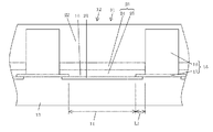
図1は、本実施の形態の発光装置11の断面図であり、図2は、発光装置11の平面図である。表示装置に用いられる通常の発光装置では、多数の有機EL素子がマトリクス状に設けられるが、本実施の形態では、理解の容易のために9個の有機EL素子12が3行3列に配列された発光装置11について説明する。また図1は、1つの有機EL素子12が形成れた領域のみを示している。
FIG. 1 is a cross-sectional view of the light-
本実施の形態の発光装置11は、基板13と、該基板13上に設けられる複数の有機EL素子12と、各有機EL素子12が設けられる各画素領域14を規定する隔壁15とを備える。
The
隔壁15は、各画素領域14に相当する領域に開口16が穿設された絶縁膜17と、該絶縁膜17の基板13とは反対側に設けられる隔壁本体18とを含んで構成される。有機EL素子12は、一対の電極21,22と、該電極21,22に挟持され、かつ前記隔壁15に囲まれる領域(画素領域14)に配置される発光部23とを含んで構成される。
The
本実施の形態ではアクティブマトリクス型の表示装置として機能する発光装置11について説明するが、発光装置11は、アクティブマトリクス型の表示装置としても、パッシブマトリクス型の表示装置としてもよい。
Although the light-
発光装置11は、m×n個(記号「m」、「n」は、それぞれ自然数を表す。本実施の形態では、m=3、n=3)の画素を備える場合、それぞれが画素として機能するm×n個の有機EL素子がm行n列のマトリクス状に配置されて構成される。
When the
基板13上には隔壁15が格子状に形成されており、この隔壁15に区分けされる領域に各有機EL素子12が設けられることにより、各有機EL素子12はマトリクス状に配置される。
基板13には、アクティブマトリクス型の表示装置用の回路が形成されたTFT(Thin Film Transistor)基板を用いることができる。各有機EL素子12は、それぞれが互いに分離した陽極21を備える。各陽極21は、基板13上において離散的にm行n列のマトリクス状に配置され、基板13に形成された回路に電気的に接続される。本実施の形態では、一対の電極21、22のうちの基板13側に設けられる一方の電極を陽極21とし、他方の電極を陰極22とする。なお、一方の電極を陰極とし、他方の電極を陽極とする構成の有機EL素子を基板に設けてもよい。
As the
基板13の厚み方向の一方から見て、陽極21は、周縁部が少なくとも絶縁膜17の端部に覆われている。なお、基板13の厚み方向の一方から見て、陽極21の周縁部が隔壁本体18の一部に重なっていてもよい。
When viewed from one side in the thickness direction of the
絶縁膜17は、膜状であって、画素領域に14相当する領域に貫通する開口が穿設されて成り、格子状に形成される。この絶縁膜17によって陽極21と陰極22とが電気的に絶縁されるので、後述する発光層24が絶縁膜17上に設けられたとしても、絶縁膜17上の発光層24は発光しない。換言すると、基板13の厚み方向の一方から見て、絶縁膜17に形成された開口16に設けられた発光部23のみが発光するので、隔壁15のうちで特に絶縁膜17に囲まれた領域が、発光可能な画素領域14に相当する。
The insulating
隔壁本体18は、本実施の形態では絶縁膜17に接して設けられる。なお、絶縁膜17と隔壁本体18との間には所定の層が介在していてもよい。隔壁本体18は、絶縁膜17上に形成され、画素領域14から退避して形成される。すなわち隔壁本体18は、基板13の厚み方向の一方から見て、絶縁膜17の内側において格子状に形成される。
The
隔壁本体18により規定される各領域には、発光部23が設けられる。この発光部23は、絶縁膜17に穿設された開口16に渡って形成され、該開口16から露出する陽極21に接して設けられる。なお絶縁膜17の厚さは、発光部23の厚さよりも薄い。したがって発光部23は、絶縁膜17に穿設された開口16だけでなく、この開口16を超えて絶縁膜17上にまで形成されている。
A light emitting unit 23 is provided in each region defined by the
陰極22は、基板13の厚み方向の一方から発光部23および隔壁本体18を覆って基板13全面にわたって形成される。すなわち各有機EL素子12の陰極22は電気的に接続されており、共通の電極として機能する。
The
次に発光装置11の製造方法について説明する。
Next, a method for manufacturing the
まず、TFT基板を用意する。TFT基板は市販のものを使用可能であり、通常、TFT基板には電極が形成されている。陽極21および基板13を通って光を取出すボトムエミッション型の有機EL素子12では、陽極21は光透過性を示す電極によって構成される。陽極21には、電気伝導度の高い金属酸化物、金属硫化物および金属などの薄膜を用いることができ、光透過率の高いものが好適に用いられる。具体的には、酸化インジウム、酸化亜鉛、酸化スズ、ITO、インジウム亜鉛酸化物(Indium Zinc Oxide:略称IZO)、金、白金、銀、および銅などから成る薄膜が用いられ、これらの中でもITO、IZO、または酸化スズから成る薄膜が好適に用いられる。陽極21の作製方法としては、真空蒸着法、スパッタリング法、イオンプレーティング法、メッキ法などを挙げることができ、これらの方法により導電膜を形成した後に、フォトリソグラフィ法によって所定のパターンに形成される。また、該陽極として、ポリアニリンもしくはその誘導体、ポリチオフェンもしくはその誘導体などの有機の透明導電膜を用いてもよい。
First, a TFT substrate is prepared. A commercially available TFT substrate can be used, and electrodes are usually formed on the TFT substrate. In the bottom emission type
陽極の膜厚は、光の透過性と電気伝導度とを考慮して、適宜選択することができ、例えば10nm〜10μmであり、好ましくは20nm〜1μmであり、さらに好ましくは50nm〜500nmである。 The film thickness of the anode can be appropriately selected in consideration of light transmittance and electrical conductivity, and is, for example, 10 nm to 10 μm, preferably 20 nm to 1 μm, and more preferably 50 nm to 500 nm. .
次に絶縁膜17を形成する。絶縁膜17は、隔壁本体18よりもインキに対して親液性を示すことが好ましく、隔壁本体18を撥液化する工程において撥液化しないように、好ましくは無機物によって構成される。絶縁膜17は、SiN、およびSiO2などから成り、好ましくはSiNから成る。
Next, an insulating
絶縁膜17は、スパッタリング法、CVD(Chemical Vapor Deposition)、マスク蒸着、およびスピンコート法などによって形成される。例えばCVDにより全面に絶縁性を示す薄膜を形成し、次にフォトレジストを塗布し、所定の領域に光を照射し、現像することによりフォトレジスト層から成る保護膜を形成し、さらにドライエッチングまたはウェットエッチングにより絶縁性を示す薄膜の画素領域14に相当する領域に開口16を穿設し、絶縁膜17を形成することができる。
The insulating
このような絶縁膜17の厚みは、発光部23よりも少なくとも薄く、50nm以下が好ましく、より好ましくは30nmであり、さらに好ましくは10nmである。絶縁膜17の厚みの下限は、絶縁膜17を構成する部材に応じて、電気絶縁性を確保できる厚さに適宜設定され、通常5nmである。
The thickness of such an insulating
絶縁膜17の幅、すなわち行方向または列方向に隣接する画素領域14の間隔は、解像度によって適宜設定され、通常、10μm〜50μm程度である。
The width of the insulating
次に隔壁本体18を形成する。隔壁本体18は、インキに対して撥液性を示すことが好ましく、フッ素含有ガス雰囲気で行うプラズマ処理のような簡易な方法で撥液化する有機物を含んで構成されることが好ましい。隔壁本体18は、例えば、アクリル樹脂系、ノボラック樹脂系、ポリイミド樹脂系のポジ型またはネガ型の感光性材料(フォトレジスト)を用いて形成することがパターニングを容易に行えるので好ましい。具体的にはフォトレジストを基板全面に塗布し、プリベーク処理を行い、所定のマスクを介して所定の領域に光を照射し、現像し、さらにポストベーク処理を行うことによって、所定の形状にパターニングされた隔壁本体18を得ることができる。フォトレジストを塗布する方法としては、スピンコーター、スリットコーターなどを用いた方法を挙げることができる。
Next, the
隔壁本体18は、さらに撥液化処理される。例えば有機物からなる隔壁本体18を形成した場合には、フッ素含有ガス雰囲気においてプラズマ処理を行うことにより表面を撥液化することができ、具体的にはCF4ガスの雰囲気においてプラズマ処理を行うことにより、表面を撥液化することができる。なおこのプラズマ処理では、無機物から成る絶縁膜17は撥液化せず、親液性を維持する。このように絶縁膜17を無機物で構成し、隔壁本体18を有機物で構成し、さらにフッ素含有ガス雰囲気においてプラズマ処理を行うことにより、撥液性を示す隔壁本体18と、親液性を示す絶縁膜17とを簡易に作り分けることができる。
The
隔壁本体18の厚みは、発光部23を塗布法により形成する際に、インキを保持可能な厚さに設定され、通常、0.5μm〜10μm程度であり、1μm〜3μmが好ましい。また隔壁本体18の幅は、絶縁膜17の幅よりも短く、10μm〜50μm程度である。
The thickness of the
次に発光部23を形成する。発光部23は、有機材料を含むインキを用いる塗布法により形成されてなる有機層を含むことが好ましい。また発光部23は、最も基板寄りに設けられる正孔注入層25を含む複数の層が積層されて構成されることが好ましく、本実施の形態では、発光部23は、正孔注入層25と、発光層24との2層の有機層が積層されて構成される。正孔注入層25は、陽極21に接して設けられ、この正孔注入層25に発光層24が接して設けられ、さらに発光層24に陰極22が接して設けられている。
Next, the light emitting part 23 is formed. It is preferable that the light emission part 23 contains the organic layer formed by the apply | coating method using the ink containing an organic material. The light emitting unit 23 is preferably configured by stacking a plurality of layers including the
正孔注入層25は、後述する正孔注入層25を形成する有機材料と、これを溶解する溶媒とを含むインキを用いる塗布法により形成される。塗布法としては、隔壁15により規定される領域に選択的にインキを供給することができる方法であれば特に制限はなく、例えばインクジェットプリント法、フレキソ印刷法などを挙げることができる。例えばインクジェットプリント装置を用いることにより、インキを所定の領域に選択的に滴下することができ、隔壁15により規定された領域にインキを選択的に供給することができる。さらに、常温または加熱下でインキを乾燥させることにより、正孔注入層25を形成することができる。
The
発光層24は、後述する発光層24を形成する有機材料と、これを溶解する溶媒とを含むインキを用いる塗布法により形成され、正孔注入層25と同様の方法により形成することができる。
The
陰極22は、仕事関数が小さく、発光層への電子注入が容易で、電気伝導度の高い材料を用いて形成することが好ましい。また陽極側から光を取出す構成の有機EL素子12では、発光層24からの光を陰極22で陽極21側に反射するために、陰極22の材料としては可視光反射率の高い材料が好ましい。陰極22には、例えばアルカリ金属、アルカリ土類金属、遷移金属およびIII−B族金属などを用いることができる。陰極の材料としては、例えばリチウム、ナトリウム、カリウム、ルビジウム、セシウム、ベリリウム、マグネシウム、カルシウム、ストロンチウム、バリウム、アルミニウム、スカンジウム、バナジウム、亜鉛、イットリウム、インジウム、セリウム、サマリウム、ユーロピウム、テルビウム、イッテルビウムなどの金属、前記金属のうちの2種以上の合金、前記金属のうちの1種以上と、金、銀、白金、銅、マンガン、チタン、コバルト、ニッケル、タングステン、錫のうちの1種以上との合金、またはグラファイト若しくはグラファイト層間化合物などが用いられる。合金の例としては、マグネシウム−銀合金、マグネシウム−インジウム合金、マグネシウム−アルミニウム合金、インジウム−銀合金、リチウム−アルミニウム合金、リチウム−マグネシウム合金、リチウム−インジウム合金、カルシウム−アルミニウム合金などを挙げることができる。また、陰極としては導電性金属酸化物および導電性有機物などから成る透明導電性電極を用いることができる。具体的には、導電性金属酸化物として酸化インジウム、酸化亜鉛、酸化スズ、ITO、およびIZOを挙げることができ、導電性有機物としてポリアニリンもしくはその誘導体、ポリチオフェンもしくはその誘導体などを挙げることができる。なお、陰極は、2層以上を積層した積層体で構成されていてもよい。
The
陰極22の膜厚は、電気伝導度や耐久性を考慮して適宜設定され、例えば10nm〜5μm程度である。本実施の形態では、外部の環境から発光部23を遮断するための保護部材としても機能する陰極22を構成するために、陰極22は厚膜に形成される。陰極22の作製方法としては、真空蒸着法、スパッタリング法、また金属薄膜を熱圧着するラミネート法などを挙げることができる。
The film thickness of the
以上説明した本実施の形態の発光装置11では、絶縁膜17の厚さを発光部23の厚さよりも薄くしている。図4に示す従来の発光装置では、絶縁膜3の膜厚が厚く、このような絶縁膜3を用いた場合、有機層5、6の膜厚が絶縁膜3の影響により不均一となり、画素領域内で均一な膜厚の有機層を形成することができなかった。有機EL素子を用いた表示装置は、液晶表示装置の技術の大部分を流用することにより発展してきたという経緯がある。液晶表示装置は市場に普及し、その要素技術は確立されたものなので、液晶表示装置に用いられている技術を敢えて変更することはせず、絶縁膜3の膜厚などは液晶表示装置のそれを踏襲していた。そのため図4に示す従来の発光装置の絶縁膜3の膜厚は、100nm〜500nm程度であった。しかしながら有機EL素子は、その特徴の一つでもあるが、薄型であるため、液晶表示装置に用いられていた絶縁膜を利用した場合、絶縁膜が発光部よりも厚くなるので、液晶表示装置の技術では問題とならなかった絶縁膜が有機層の形成において大きく影響する。そこで本実施の形態では発光部23よりも薄い絶縁膜17を形成することにより、正孔注入層25、発光層24などの有機層を塗布法により形成する際に、絶縁膜17の影響を小さいものとすることができ、結果として均一な膜厚の有機層を形成することができる。特に、発光部23を構成する各有機層は、それぞれが絶縁膜17よりも厚みが厚い方が好ましく、例えば従来の技術では、親液性の絶縁膜3に引きずられながらインキが乾くので、有機層5において絶縁膜3の端部付近(図4参照)に絶縁膜3の影響が大きく現れるが、本実施の形態では各有機層が絶縁膜17よりも厚いため、そもそも絶縁膜17の側面が有機層の形成にほとんど影響しないので、均一な膜厚の有機層を形成することができる。これによって発光不良の抑制された有機EL素子12を得ることができ、性能の高い発光装置11を実現することができる。特に発光部23を構成する複数の層のうちで最も基板寄りの層が電気抵抗の低い正孔注入層16である場合、図4に示す従来の技術のように絶縁膜17の端部付近で膜厚が不均一になると、正孔注入層16と陰極22との間隔が狭くなるか、場合によっては正孔注入層16と陰極22とが接触することがあるので、素子の構造として発光時にリーク電流が生じる可能性が高くなる。しかしながら本実施の形態では、塗布法で各有機層を形成したとしても、各有機層が絶縁膜17よりも厚いために、均一な膜厚の有機層を形成することができるので、リーク電流などが抑制された有機EL素子12を得ることができ、性能の高い発光装置11を実現することができる。
In the
このような絶縁膜17としては、厚みが、100nm未満であることが好ましく、このような厚みの絶縁膜17を形成することによって、発光部23を形成する際の絶縁膜17の影響を小さくすることができ、膜厚が均一な有機層を得ることができる。
Such an insulating
さらに、絶縁膜17は、開口16に臨む前記絶縁膜17の側面により画成される開口16が、基板に近接する向きに順テーパ状であることが好ましい。このようにテーパ状の絶縁膜17を形成することにより、絶縁膜17の端部がなだらかになり、絶縁膜17の端部により形成される段差部が発光部23を形成する際の絶縁膜17の影響をさらに小さくすることができ、膜厚がより均一な有機層を得ることができる。
Further, it is preferable that the insulating
テーパ状の絶縁膜17は、例えば所定のドライエッチングにより形成することができる。図3にテーパ状の絶縁膜17を形成する工程を模式的に示す。まず前述したようにSiNなどから成る絶縁性を示す薄膜31をCVDなどによって全面に形成する。CVDでは、10nm〜20nm程度の薄膜31を形成することが可能であり、10nm〜20nm以上の膜厚の薄膜31を適宜形成することができる。次に、絶縁性を示す薄膜31上にフォトレジスト32を全面に塗布し(図3(1)参照)、次にプリベーク、露光、現像、ポストベークなどの所定の処理を行い、絶縁性を示す薄膜31のうちの画素領域上に形成された部分を除去する。フォトレジスト32を用いて形成される保護膜33の側面33aは、絶縁性を示す薄膜31の表面に対して垂直ではなく、図3(2)に示すように、絶縁性を示す薄膜31の表面に対して傾斜しており、その角度θは、10°〜60°程度である。通常のドライエッチングは、異方性エッチングなので、例えばCF4ガスを導入したプラズマエッチングを行うと、絶縁性を示す薄膜31に、基板13に垂直な貫通孔が形成される。すなわち貫通孔を囲う薄膜31の側面が、基板13に垂直となる。しかしながらCF4に加えてO2を導入した雰囲気でプラズマエッチングを行うと、図3(3)に示すように、エッチングの際に、絶縁性を示す薄膜31だけでなく、保護膜33までエッチングされるので、保護膜33によって保護される領域が矢印で示すように移動しつつ、絶縁性を示す薄膜31が削られることになり、結果としてテーパ状の絶縁膜17が形成される。絶縁膜17の画素領域14に臨む側面と陽極21表面との成す角度ψは、10°〜60°であることが好ましい。この角度ψの調整は、保護膜33の材料、保護膜33の傾斜角度θ、エッチングの際に導入するCF4、O2ガスの流量などを適宜設定することにより可能であり、特に、エッチングの際に導入するO2ガスの流量を調整することにより、角度ψを調整することができ、具体的にはO2ガスの流量を多くするほど、角度ψが小さくなる傾向にある。
The tapered insulating
また基板13の厚み方向の一方から見て、絶縁膜17の画素領域14に臨む側面と、前記隔壁本体18の画素領域14に臨む側面との間隔L1が、1μm以上であることが好ましい(図1参照)。隔壁本体18は、インキを収容する機能を発揮するために、通常、その表面がインキに対して撥液性を示すように形成されているので、供給されたインキが隔壁本体18に弾かれつつ乾燥する。そうすると、隔壁本体18近傍で有機層の膜厚が薄くなるなど、膜厚の均一性が悪くなる。隔壁本体18とは別に所定の絶縁膜17を設ける理由の1つは、隔壁本体18近傍での膜厚の不均一性に起因する素子の発光特性の低下を抑制することにある。しかしながら、隔壁本体18から絶縁膜17が突出する部分が小さいと、隔壁本体18の影響が、画素領域14における有機層の膜厚分布に顕在化することになる。そこで間隔L1を1μm以上に設定することにより、画素領域14における有機層の膜厚分布に隔壁本体18が与える影響を小さくすることができ、画素領域14において膜厚が均一な有機層を形成することができる。なお間隔L1は、解像度などの設計により適宜設定されるが、広すぎると開口率が小さくなるので、その上限は、通常5μm程度である。
In addition, when viewed from one side in the thickness direction of the
以上説明した本実施の形態の発光装置11における有機EL素子は、「陽極/正孔注入層/発光層/陰極」の層構成を有しているが、有機EL素子は、一対の電極と、該電極間に発光層を備えていれば、本実施の形態における有機EL素子とは異なる素子構成であってもよい。以下に陽極と陰極との間に設けられうる層について説明するが、これらの層のうち、有機物を含む層であって、該層を形成する有機材料が溶媒に溶解可能なものであれば、前述したインクジェットプリント法などの塗布法により、均一な膜厚の有機層としてこれらの層を形成することができる。なお陽極と陰極との間に設けられる発光部は、塗布法により形成される1または複数の有機層のみからなることが好ましい。このように発光部を有機層のみにより構成することにより、工程が簡易な塗布法によって発光部を形成することができ、工程が簡易になる。
The organic EL element in the
陰極と発光層との間に設けられる層としては、電子注入層、電子輸送層、正孔ブロック層などを挙げることができる。陰極と発光層との間に、一層のみが設けられる場合には、該層を電子注入層という。また陰極と発光層との間に電子注入層と電子輸送層との両方の層が設けられる場合、陰極に接する層を電子注入層といい、この電子注入層を除く層を電子輸送層という。 Examples of the layer provided between the cathode and the light emitting layer include an electron injection layer, an electron transport layer, and a hole blocking layer. When only one layer is provided between the cathode and the light emitting layer, the layer is referred to as an electron injection layer. When both the electron injection layer and the electron transport layer are provided between the cathode and the light emitting layer, a layer in contact with the cathode is referred to as an electron injection layer, and a layer excluding the electron injection layer is referred to as an electron transport layer.
電子注入層は、陰極からの電子注入効率を改善する機能を有する層である。電子輸送層は、陰極、電子注入層または陰極により近い電子輸送層からの電子注入を改善する機能を有する層である。正孔ブロック層は、正孔の輸送を堰き止める機能を有する層である。なお電子注入層、及び/又は電子輸送層が正孔の輸送を堰き止める機能を有する場合には、これらの層が正孔ブロック層を兼ねることがある。 The electron injection layer is a layer having a function of improving electron injection efficiency from the cathode. The electron transport layer is a layer having a function of improving electron injection from the cathode, the electron injection layer, or the electron transport layer closer to the cathode. The hole blocking layer is a layer having a function of blocking hole transport. In the case where the electron injection layer and / or the electron transport layer have a function of blocking hole transport, these layers may also serve as the hole blocking layer.
正孔ブロック層が正孔の輸送を堰き止める機能を有することは、例えばホール電流のみを流す素子を作製し、その電流値の減少で堰き止める効果を確認することが可能である。 The fact that the hole blocking layer has a function of blocking hole transport makes it possible, for example, to produce an element that allows only a hole current to flow, and confirm the blocking effect by reducing the current value.
陽極と発光層との間に設けられる層としては、正孔注入層、正孔輸送層、電子ブロック層などを挙げることができる。陽極と発光層との間に、正孔注入層と正孔輸送層との両方の層が設けられる場合、陽極に接する層を正孔注入層といい、この正孔注入層を除く層を正孔輸送層という。 Examples of the layer provided between the anode and the light emitting layer include a hole injection layer, a hole transport layer, and an electron block layer. When both the hole injection layer and the hole transport layer are provided between the anode and the light-emitting layer, the layer in contact with the anode is called a hole injection layer, and the layers other than the hole injection layer are positive. It is called a hole transport layer.
正孔注入層は、陽極からの正孔注入効率を改善する機能を有する層である。正孔輸送層は、陽極、正孔注入層または陽極により近い正孔輸送層からの正孔注入を改善する機能を有する層である。電子ブロック層は、電子の輸送を堰き止める機能を有する層である。なお正孔注入層、及び/又は正孔輸送層が電子の輸送を堰き止める機能を有する場合には、これらの層が電子ブロック層を兼ねることがある。 The hole injection layer is a layer having a function of improving hole injection efficiency from the anode. The hole transport layer is a layer having a function of improving hole injection from the anode, the hole injection layer, or the hole transport layer closer to the anode. The electron blocking layer is a layer having a function of blocking electron transport. In the case where the hole injection layer and / or the hole transport layer has a function of blocking electron transport, these layers may also serve as an electron blocking layer.
電子ブロック層が電子の輸送を堰き止める機能を有することは、例えば、電子電流のみを流す素子を作製し、その電流値の減少で堰き止める効果を確認することが可能である。 The fact that the electron blocking layer has a function of blocking electron transport makes it possible, for example, to produce an element that allows only electron current to flow and confirm the blocking effect by reducing the current value.
なお、電子注入層および正孔注入層を総称して電荷注入層と言う場合があり、電子輸送層および正孔輸送層を総称して電荷輸送層と言う場合がある。 The electron injection layer and the hole injection layer may be collectively referred to as a charge injection layer, and the electron transport layer and the hole transport layer may be collectively referred to as a charge transport layer.
本実施の形態の有機EL素子のとりうる層構成の一例を以下に示す。
a)陽極/発光層/陰極
b)陽極/正孔注入層/発光層/陰極
c)陽極/正孔注入層/発光層/電子注入層/陰極
e)陽極/正孔注入層/発光層/電子輸送層/陰極
f)陽極/正孔注入層/発光層/電子輸送層/電子注入層/陰極
d)陽極/正孔輸送層/発光層/陰極
e)陽極/正孔輸送層/発光層/電子注入層/陰極
f)陽極/正孔輸送層/発光層/電子輸送層/陰極
g)陽極/正孔輸送層/発光層/電子輸送層/電子注入層/陰極
h)陽極/正孔注入層/正孔輸送層/発光層/陰極
i)陽極/正孔注入層/正孔輸送層/発光層/電子注入層/陰極
j)陽極/正孔注入層/正孔輸送層/発光層/電子輸送層/陰極
k)陽極/正孔注入層/正孔輸送層/発光層/電子輸送層/電子注入層/陰極
l)陽極/発光層/電子注入層/陰極
m)陽極/発光層/電子輸送層/陰極
n)陽極/発光層/電子輸送層/電子注入層/陰極
(ここで、記号「/」は、記号「/」を挟む各層が隣接して積層されていることを示す。以下同じ。)
本実施の形態の有機EL素子は、2層以上の発光層を有していてもよく、2層の発光層を有する有機EL素子としては、上記a)〜n)の層構成のうちのいずれか1つにおいて、陽極と陰極とに挟持された積層体を「繰り返し単位A」とすると、以下のo)に示す層構成を挙げることができる。
o)陽極/(繰り返し単位A)/電荷注入層/(繰り返し単位A)/陰極
また、3層以上の発光層を有する有機EL素子としては、「(繰り返し単位A)/電荷注入層」を「繰り返し単位B」とすると、以下のp)に示す層構成を挙げることができる。
p)陽極/(繰り返し単位B)x/(繰り返し単位A)/陰極
なお記号「x」は、2以上の整数を表し、(繰り返し単位B)xは、繰り返し単位Bがx段積層された積層体を表す。
An example of a layer structure that can be taken by the organic EL element of the present embodiment is shown below.
a) anode / light emitting layer / cathode b) anode / hole injection layer / light emitting layer / cathode c) anode / hole injection layer / light emitting layer / electron injection layer / cathode e) anode / hole injection layer / light emitting layer / Electron transport layer / cathode f) anode / hole injection layer / light emitting layer / electron transport layer / electron injection layer / cathode d) anode / hole transport layer / light emitting layer / cathode e) anode / hole transport layer / light emitting layer / Electron injection layer / cathode f) anode / hole transport layer / light emitting layer / electron transport layer / cathode g) anode / hole transport layer / light emitting layer / electron transport layer / electron injection layer / cathode h) anode / hole Injection layer / hole transport layer / light emitting layer / cathode i) anode / hole injection layer / hole transport layer / light emitting layer / electron injection layer / cathode j) anode / hole injection layer / hole transport layer / light emitting layer / Electron transport layer / cathode k) anode / hole injection layer / hole transport layer / light emitting layer / electron transport layer / electron injection layer / cathode l) anode / light emitting layer / electron injection layer / cathode m) anode / Photo layer / electron transport layer / cathode n) anode / light emitting layer / electron transport layer / electron injection layer / cathode (here, the symbol “/” indicates that each layer sandwiching the symbol “/” is laminated adjacently) The same shall apply hereinafter.)
The organic EL device of the present embodiment may have two or more light-emitting layers, and as an organic EL device having two light-emitting layers, any one of the layer configurations a) to n) above. In such a case, when the laminate sandwiched between the anode and the cathode is referred to as “repeating unit A”, the following layer configuration shown in o) can be given.
o) Anode / (Repeating Unit A) / Charge Injection Layer / (Repeating Unit A) / Cathode Further, as an organic EL device having three or more light emitting layers, “(Repeating Unit A) / Charge Injection Layer” As the “repeating unit B”, the layer structure shown in the following p) can be exemplified.
p) Anode / (Repeating unit B) x / (Repeating unit A) / Cathode The symbol “x” represents an integer of 2 or more, and (Repeating unit B) x is a laminate in which the repeating unit B is laminated in x stages. Represents the body.
ここで、電荷注入層とは電界を印加することにより、正孔と電子を発生する層である。電荷発生層としては、例えば酸化バナジウム、インジウムスズ酸化物(Indium Tin Oxide:略称ITO)、酸化モリブデンなどから成る薄膜を挙げることができる。 Here, the charge injection layer is a layer that generates holes and electrons by applying an electric field. Examples of the charge generation layer include a thin film made of vanadium oxide, indium tin oxide (abbreviated as ITO), molybdenum oxide, or the like.
本実施の形態の有機EL素子は、さらに電極との密着性向上や電極からの電荷注入性の改善のために、電極に隣接して膜厚2nm以下の絶縁層を設けてもよい。また界面での密着性向上や混合の防止などのために、前述した各層間に薄いバッファー層を挿入してもよい。 In the organic EL element of the present embodiment, an insulating layer having a thickness of 2 nm or less may be provided adjacent to the electrode in order to further improve the adhesion to the electrode and the charge injection property from the electrode. In addition, a thin buffer layer may be inserted between each of the aforementioned layers in order to improve adhesion at the interface or prevent mixing.
積層する層の順序、層数、および各層の厚さについては、発光効率や素子寿命を勘案して適宜設定することができる。 The order of the layers to be laminated, the number of layers, and the thickness of each layer can be appropriately set in consideration of the light emission efficiency and the element lifetime.
次に、有機EL素子を構成する各層の材料および形成方法について、より具体的に説明する。 Next, the material and forming method of each layer constituting the organic EL element will be described more specifically.
<正孔注入層>
正孔注入層を構成する正孔注入材料としては、酸化バナジウム、酸化モリブデン、酸化ルテニウム、および酸化アルミニウムなどの酸化物や、フェニルアミン系、スターバースト型アミン系、フタロシアニン系、アモルファスカーボン、ポリアニリン、およびポリチオフェン誘導体などを挙げることができる。
<Hole injection layer>
As the hole injection material constituting the hole injection layer, oxides such as vanadium oxide, molybdenum oxide, ruthenium oxide, and aluminum oxide, phenylamine type, starburst type amine type, phthalocyanine type, amorphous carbon, polyaniline, And polythiophene derivatives.
正孔注入層の成膜方法としては、例えば正孔注入材料を含む溶液からの成膜を挙げることができる。溶液からの成膜に用いられる溶媒としては、正孔注入材料を溶解させるものであれば特に制限はなく、クロロホルム、塩化メチレン、ジクロロエタンなどの塩素系溶媒、テトラヒドロフランなどのエーテル系溶媒、トルエン、キシレンなどの芳香族炭化水素系溶媒、アセトン、メチルエチルケトンなどのケトン系溶媒、酢酸エチル、酢酸ブチル、エチルセルソルブアセテートなどのエステル系溶媒、および水を挙げることができる。 Examples of the method for forming the hole injection layer include film formation from a solution containing a hole injection material. The solvent used for film formation from a solution is not particularly limited as long as it dissolves the hole injection material. Chlorine solvents such as chloroform, methylene chloride, dichloroethane, ether solvents such as tetrahydrofuran, toluene, xylene And aromatic hydrocarbon solvents such as acetone, ketone solvents such as acetone and methyl ethyl ketone, ester solvents such as ethyl acetate, butyl acetate and ethyl cellosolve acetate, and water.
溶液からの成膜方法としては、スピンコート法、キャスティング法、マイクログラビアコート法、グラビアコート法、バーコート法、ロールコート法、ワイアーバーコート法、ディップコート法、スプレーコート法、スクリーン印刷法、フレキソ印刷法、オフセット印刷法、インクジェットプリント法などの塗布法を挙げることができる。 As a film forming method from a solution, a spin coating method, a casting method, a micro gravure coating method, a gravure coating method, a bar coating method, a roll coating method, a wire bar coating method, a dip coating method, a spray coating method, a screen printing method, Examples of the application method include a flexographic printing method, an offset printing method, and an ink jet printing method.
正孔注入層の膜厚は、用いる材料によって最適値が異なり、駆動電圧と発光効率が適度な値となるように適宜設定され、少なくともピンホールが発生しないような厚さが必要であり、あまり厚いと、素子の駆動電圧が高くなるので好ましくない。従って正孔注入層の膜厚は、例えば1nm〜1μmであり、好ましくは2nm〜500nmであり、さらに好ましくは5nm〜200nmである。 The film thickness of the hole injection layer varies depending on the material used, and is set as appropriate so that the drive voltage and light emission efficiency are appropriate. If it is thick, the driving voltage of the element increases, which is not preferable. Therefore, the film thickness of the hole injection layer is, for example, 1 nm to 1 μm, preferably 2 nm to 500 nm, and more preferably 5 nm to 200 nm.
<正孔輸送層>
正孔輸送層を構成する正孔輸送材料としては、ポリビニルカルバゾール若しくはその誘導体、ポリシラン若しくはその誘導体、側鎖若しくは主鎖に芳香族アミンを有するポリシロキサン誘導体、ピラゾリン誘導体、アリールアミン誘導体、スチルベン誘導体、トリフェニルジアミン誘導体、ポリアニリン若しくはその誘導体、ポリチオフェン若しくはその誘導体、ポリアリールアミン若しくはその誘導体、ポリピロール若しくはその誘導体、ポリ(p−フェニレンビニレン)若しくはその誘導体、又はポリ(2,5−チエニレンビニレン)若しくはその誘導体などを挙げることができる。
<Hole transport layer>
As the hole transport material constituting the hole transport layer, polyvinylcarbazole or a derivative thereof, polysilane or a derivative thereof, a polysiloxane derivative having an aromatic amine in a side chain or a main chain, a pyrazoline derivative, an arylamine derivative, a stilbene derivative, Triphenyldiamine derivative, polyaniline or derivative thereof, polythiophene or derivative thereof, polyarylamine or derivative thereof, polypyrrole or derivative thereof, poly (p-phenylene vinylene) or derivative thereof, or poly (2,5-thienylene vinylene) or Examples thereof include derivatives thereof.
これらの中で正孔輸送材料としては、ポリビニルカルバゾール若しくはその誘導体、ポリシラン若しくはその誘導体、側鎖若しくは主鎖に芳香族アミン化合物基を有するポリシロキサン誘導体、ポリアニリン若しくはその誘導体、ポリチオフェン若しくはその誘導体、ポリアリールアミン若しくはその誘導体、ポリ(p−フェニレンビニレン)若しくはその誘導体、又はポリ(2,5−チエニレンビニレン)若しくはその誘導体などの高分子正孔輸送材料が好ましく、さらに好ましくはポリビニルカルバゾール若しくはその誘導体、ポリシラン若しくはその誘導体、側鎖若しくは主鎖に芳香族アミンを有するポリシロキサン誘導体である。低分子の正孔輸送材料の場合には、高分子バインダーに分散させて用いることが好ましい。 Among these, hole transport materials include polyvinyl carbazole or derivatives thereof, polysilane or derivatives thereof, polysiloxane derivatives having aromatic amine compound groups in the side chain or main chain, polyaniline or derivatives thereof, polythiophene or derivatives thereof, poly Polymeric hole transport materials such as arylamine or derivatives thereof, poly (p-phenylene vinylene) or derivatives thereof, or poly (2,5-thienylene vinylene) or derivatives thereof are preferred, and polyvinylcarbazole or derivatives thereof are more preferred. , Polysilane or a derivative thereof, and a polysiloxane derivative having an aromatic amine in the side chain or main chain. In the case of a low-molecular hole transport material, it is preferably used by being dispersed in a polymer binder.
正孔輸送層の成膜方法としては、特に制限はないが、低分子の正孔輸送材料では、高分子バインダーと正孔輸送材料とを含む混合液からの成膜を挙げることができ、高分子の正孔輸送材料では、正孔輸送材料を含む溶液からの成膜を挙げることができる。 The method for forming the hole transport layer is not particularly limited, but in the case of a low molecular hole transport material, film formation from a mixed solution containing a polymer binder and a hole transport material can be exemplified. Examples of molecular hole transport materials include film formation from a solution containing a hole transport material.
溶液からの成膜に用いられる溶媒としては、正孔輸送材料を溶解させるものであれば特に制限はなく、クロロホルム、塩化メチレン、ジクロロエタンなどの塩素系溶媒、テトラヒドロフランなどのエーテル系溶媒、トルエン、キシレンなどの芳香族炭化水素系溶媒、アセトン、メチルエチルケトンなどのケトン系溶媒、酢酸エチル、酢酸ブチル、エチルセルソルブアセテートなどのエステル系溶媒などを挙げることができる。 The solvent used for film formation from a solution is not particularly limited as long as it can dissolve a hole transport material. Chlorine solvents such as chloroform, methylene chloride, dichloroethane, ether solvents such as tetrahydrofuran, toluene, xylene And aromatic hydrocarbon solvents such as acetone, ketone solvents such as acetone and methyl ethyl ketone, and ester solvents such as ethyl acetate, butyl acetate, and ethyl cellosolve acetate.
溶液からの成膜方法としては、前述した正孔中注入層の成膜法と同様の塗布法を挙げることができる。 Examples of the film forming method from a solution include the same coating method as the above-described film forming method of the in-hole injection layer.
混合する高分子バインダーとしては、電荷輸送を極度に阻害しないものが好ましく、また可視光に対する吸収の弱いものが好適に用いられ、例えばポリカーボネート、ポリアクリレート、ポリメチルアクリレート、ポリメチルメタクリレート、ポリスチレン、ポリ塩化ビニル、ポリシロキサンなどを挙げることができる。 As the polymer binder to be mixed, those that do not extremely inhibit charge transport are preferable, and those that weakly absorb visible light are preferably used. For example, polycarbonate, polyacrylate, polymethyl acrylate, polymethyl methacrylate, polystyrene, poly Examples thereof include vinyl chloride and polysiloxane.
正孔輸送層の膜厚としては、用いる材料によって最適値が異なり、駆動電圧と発光効率が適度な値となるように適宜設定され、少なくともピンホールが発生しないような厚さが必要であり、あまり厚いと、素子の駆動電圧が高くなり好ましくない。従って、該正孔輸送層の膜厚は、例えば1nm〜1μmであり、好ましくは2nm〜500nmであり、さらに好ましくは5nm〜200nmである。 As the film thickness of the hole transport layer, the optimum value varies depending on the material to be used, the drive voltage and the light emission efficiency are appropriately set so as to have an appropriate value, and at least a thickness that does not cause pinholes is required. If the thickness is too thick, the drive voltage of the element becomes high, which is not preferable. Therefore, the film thickness of the hole transport layer is, for example, 1 nm to 1 μm, preferably 2 nm to 500 nm, and more preferably 5 nm to 200 nm.
<発光層>
発光層は、通常、主として蛍光及び/又はりん光を発光する有機物、または該有機物とこれを補助するドーパントとから形成される。ドーパントは、例えば発光効率の向上や、発光波長を変化させるために加えられる。なお、有機物は、低分子化合物でも高分子化合物でもよく、発光層は、ポリスチレン換算の数平均分子量が、103〜108である高分子化合物を含むことが好ましい。発光層を構成する発光材料としては、例えば以下の色素系材料、金属錯体系材料、高分子系材料、ドーパント材料を挙げることができる。
(色素系材料)
色素系材料としては、例えば、シクロペンダミン誘導体、テトラフェニルブタジエン誘導体化合物、トリフェニルアミン誘導体、オキサジアゾール誘導体、ピラゾロキノリン誘導体、ジスチリルベンゼン誘導体、ジスチリルアリーレン誘導体、ピロール誘導体、チオフェン環化合物、ピリジン環化合物、ペリノン誘導体、ペリレン誘導体、オリゴチオフェン誘導体、トリフマニルアミン誘導体、オキサジアゾールダイマー、ピラゾリンダイマー、キナクリドン誘導体、クマリン誘導体などを挙げることができる。
(金属錯体系材料)
金属錯体系材料としては、例えば中心金属に、Al、Zn、Beなど、またはTb、Eu、Dyなどの希土類金属を有し、配位子にオキサジアゾール、チアジアゾール、フェニルピリジン、フェニルベンゾイミダゾール、キノリン構造などを有する金属錯体を挙げることができ、例えばイリジウム錯体、白金錯体などの三重項励起状態からの発光を有する金属錯体、アルミキノリノール錯体、ベンゾキノリノールベリリウム錯体、ベンゾオキサゾリル亜鉛錯体、ベンゾチアゾール亜鉛錯体、アゾメチル亜鉛錯体、ポルフィリン亜鉛錯体、ユーロピウム錯体などを挙げることができる。
(高分子系材料)
高分子系材料としては、ポリパラフェニレンビニレン誘導体、ポリチオフェン誘導体、ポリパラフェニレン誘導体、ポリシラン誘導体、ポリアセチレン誘導体、ポリフルオレン誘導体、ポリビニルカルバゾール誘導体、上記色素系材料や金属錯体系発光材料を高分子化したものなどを挙げることができる。
<Light emitting layer>
The light emitting layer is usually formed of an organic substance that mainly emits fluorescence and / or phosphorescence, or an organic substance and a dopant that assists the organic substance. The dopant is added, for example, in order to improve the luminous efficiency and change the emission wavelength. The organic substance may be a low molecular compound or a high molecular compound, and the light emitting layer preferably contains a high molecular compound having a polystyrene-equivalent number average molecular weight of 10 3 to 10 8 . Examples of the light emitting material constituting the light emitting layer include the following dye materials, metal complex materials, polymer materials, and dopant materials.
(Dye material)
Examples of dye-based materials include cyclopentamine derivatives, tetraphenylbutadiene derivative compounds, triphenylamine derivatives, oxadiazole derivatives, pyrazoloquinoline derivatives, distyrylbenzene derivatives, distyrylarylene derivatives, pyrrole derivatives, thiophene ring compounds. Pyridine ring compounds, perinone derivatives, perylene derivatives, oligothiophene derivatives, trifumanylamine derivatives, oxadiazole dimers, pyrazoline dimers, quinacridone derivatives, coumarin derivatives, and the like.
(Metal complex materials)
Examples of the metal complex material include Al, Zn, Be, etc. as a central metal, or rare earth metals such as Tb, Eu, Dy, etc., and oxadiazole, thiadiazole, phenylpyridine, phenylbenzimidazole, as a ligand, Examples include metal complexes having a quinoline structure, such as metal complexes having light emission from triplet excited states such as iridium complexes and platinum complexes, aluminum quinolinol complexes, benzoquinolinol beryllium complexes, benzoxazolyl zinc complexes, benzoates. Examples include a thiazole zinc complex, an azomethyl zinc complex, a porphyrin zinc complex, and a europium complex.
(Polymer material)
As polymer materials, polyparaphenylene vinylene derivatives, polythiophene derivatives, polyparaphenylene derivatives, polysilane derivatives, polyacetylene derivatives, polyfluorene derivatives, polyvinyl carbazole derivatives, the above dye materials and metal complex light emitting materials are polymerized. The thing etc. can be mentioned.
上記発光性材料のうち、青色に発光する材料としては、ジスチリルアリーレン誘導体、オキサジアゾール誘導体、およびそれらの重合体、ポリビニルカルバゾール誘導体、ポリパラフェニレン誘導体、ポリフルオレン誘導体などを挙げることができる。なかでも高分子材料のポリビニルカルバゾール誘導体、ポリパラフェニレン誘導体やポリフルオレン誘導体などが好ましい。 Among the light emitting materials, examples of the material that emits blue light include distyrylarylene derivatives, oxadiazole derivatives, and polymers thereof, polyvinylcarbazole derivatives, polyparaphenylene derivatives, and polyfluorene derivatives. Of these, polymer materials such as polyvinyl carbazole derivatives, polyparaphenylene derivatives, and polyfluorene derivatives are preferred.
また、緑色に発光する材料としては、キナクリドン誘導体、クマリン誘導体、およびそれらの重合体、ポリパラフェニレンビニレン誘導体、ポリフルオレン誘導体などを挙げることができる。なかでも高分子材料のポリパラフェニレンビニレン誘導体、ポリフルオレン誘導体などが好ましい。 Examples of materials that emit green light include quinacridone derivatives, coumarin derivatives, and polymers thereof, polyparaphenylene vinylene derivatives, polyfluorene derivatives, and the like. Of these, polymer materials such as polyparaphenylene vinylene derivatives and polyfluorene derivatives are preferred.
また、赤色に発光する材料としては、クマリン誘導体、チオフェン環化合物、およびそれらの重合体、ポリパラフェニレンビニレン誘導体、ポリチオフェン誘導体、ポリフルオレン誘導体などを挙げることができる。なかでも高分子材料のポリパラフェニレンビニレン誘導体、ポリチオフェン誘導体、ポリフルオレン誘導体などが好ましい。
(ドーパント材料)
ドーパント材料としては、例えばペリレン誘導体、クマリン誘導体、ルブレン誘導体、キナクリドン誘導体、スクアリウム誘導体、ポルフィリン誘導体、スチリル系色素、テトラセン誘導体、ピラゾロン誘導体、デカシクレン、フェノキサゾンなどを挙げることができる。なお、このような発光層の厚さは、通常約2nm〜200nmである。
Examples of materials that emit red light include coumarin derivatives, thiophene ring compounds, and polymers thereof, polyparaphenylene vinylene derivatives, polythiophene derivatives, and polyfluorene derivatives. Among these, polymer materials such as polyparaphenylene vinylene derivatives, polythiophene derivatives, and polyfluorene derivatives are preferable.
(Dopant material)
Examples of the dopant material include perylene derivatives, coumarin derivatives, rubrene derivatives, quinacridone derivatives, squalium derivatives, porphyrin derivatives, styryl dyes, tetracene derivatives, pyrazolone derivatives, decacyclene, phenoxazone, and the like. In addition, the thickness of such a light emitting layer is usually about 2 nm-200 nm.
<電子輸送層>
電子輸送層を構成する電子輸送材料としては、公知のものを使用でき、オキサジアゾール誘導体、アントラキノジメタン若しくはその誘導体、ベンゾキノン若しくはその誘導体、ナフトキノン若しくはその誘導体、アントラキノン若しくはその誘導体、テトラシアノアンスラキノジメタン若しくはその誘導体、フルオレノン誘導体、ジフェニルジシアノエチレン若しくはその誘導体、ジフェノキノン誘導体、又は8−ヒドロキシキノリン若しくはその誘導体の金属錯体、ポリキノリン若しくはその誘導体、ポリキノキサリン若しくはその誘導体、ポリフルオレン若しくはその誘導体などを挙げることができる。
<Electron transport layer>
As the electron transport material constituting the electron transport layer, known materials can be used, such as oxadiazole derivatives, anthraquinodimethane or derivatives thereof, benzoquinone or derivatives thereof, naphthoquinone or derivatives thereof, anthraquinones or derivatives thereof, tetracyanoanthra Quinodimethane or derivatives thereof, fluorenone derivatives, diphenyldicyanoethylene or derivatives thereof, diphenoquinone derivatives, or metal complexes of 8-hydroxyquinoline or derivatives thereof, polyquinoline or derivatives thereof, polyquinoxaline or derivatives thereof, polyfluorene or derivatives thereof, etc. Can be mentioned.
これらのうち、電子輸送材料としては、オキサジアゾール誘導体、ベンゾキノン若しくはその誘導体、アントラキノン若しくはその誘導体、又は8−ヒドロキシキノリン若しくはその誘導体の金属錯体、ポリキノリン若しくはその誘導体、ポリキノキサリン若しくはその誘導体、ポリフルオレン若しくはその誘導体が好ましく、2−(4−ビフェニリル)−5−(4−t−ブチルフェニル)−1,3,4−オキサジアゾール、ベンゾキノン、アントラキノン、トリス(8−キノリノール)アルミニウム、ポリキノリンがさらに好ましい。 Among these, as an electron transport material, an oxadiazole derivative, benzoquinone or a derivative thereof, anthraquinone or a derivative thereof, a metal complex of 8-hydroxyquinoline or a derivative thereof, a polyquinoline or a derivative thereof, a polyquinoxaline or a derivative thereof, a polyfluorene Or a derivative thereof is preferable, and 2- (4-biphenylyl) -5- (4-t-butylphenyl) -1,3,4-oxadiazole, benzoquinone, anthraquinone, tris (8-quinolinol) aluminum, and polyquinoline are further included. preferable.
電子輸送層の成膜法としては特に制限はないが、低分子の電子輸送材料では、粉末からの真空蒸着法、または溶液若しくは溶融状態からの成膜を挙げることができ、高分子の電子輸送材料では溶液または溶融状態からの成膜を挙げることができる。なお溶液または溶融状態からの成膜する場合には、高分子バインダーを併用してもよい。溶液から電子輸送層を成膜する方法としては、前述の溶液から正孔輸送層を成膜する方法と同様の成膜法を挙げることができる。 There are no particular restrictions on the method for forming the electron transport layer, but for low molecular weight electron transport materials, vacuum deposition from powder or film formation from a solution or a molten state can be used. Examples of the material include film formation from a solution or a molten state. In the case of forming a film from a solution or a molten state, a polymer binder may be used in combination. Examples of the method for forming an electron transport layer from a solution include the same film formation method as the method for forming a hole transport layer from a solution described above.
電子輸送層の膜厚は、用いる材料によって最適値が異なり、駆動電圧と発光効率が適度な値となるように適宜設定され、少なくともピンホールが発しないような厚さが必要であり、あまり厚いと、素子の駆動電圧が高くなり好ましくない。従って該電子輸送層の膜厚としては、例えば1nm〜1μmであり、好ましくは2nm〜500nmであり、さらに好ましくは5nm〜200nmである。 The film thickness of the electron transport layer varies depending on the material used, and is set appropriately so that the drive voltage and the light emission efficiency are appropriate, and at least a thickness that does not cause pinholes is required, and is too thick. In such a case, the driving voltage of the element increases, which is not preferable. Therefore, the film thickness of the electron transport layer is, for example, 1 nm to 1 μm, preferably 2 nm to 500 nm, and more preferably 5 nm to 200 nm.
<電子注入層>
電子注入層を構成する材料としては、発光層の種類に応じて最適な材料が適宜選択され、アルカリ金属、アルカリ土類金属、アルカリ金属およびアルカリ土類金属のうちの1種類以上含む合金、アルカリ金属若しくはアルカリ土類金属の酸化物、ハロゲン化物、炭酸化物、またはこれらの物質の混合物などを挙げることができる。アルカリ金属、アルカリ金属の酸化物、ハロゲン化物、および炭酸化物の例としては、リチウム、ナトリウム、カリウム、ルビジウム、セシウム、酸化リチウム、フッ化リチウム、酸化ナトリウム、フッ化ナトリウム、酸化カリウム、フッ化カリウム、酸化ルビジウム、フッ化ルビジウム、酸化セシウム、フッ化セシウム、炭酸リチウムなどを挙げることができる。また、アルカリ土類金属、アルカリ土類金属の酸化物、ハロゲン化物、炭酸化物の例としては、マグネシウム、カルシウム、バリウム、ストロンチウム、酸化マグネシウム、フッ化マグネシウム、酸化カルシウム、フッ化カルシウム、酸化バリウム、フッ化バリウム、酸化ストロンチウム、フッ化ストロンチウム、炭酸マグネシウムなどを挙げることができる。電子注入層は、2層以上を積層した積層体で構成されてもよく、例えばLiF/Caなどを挙げることができる。電子注入層は、蒸着法、スパッタリング法、印刷法などにより形成される。電子注入層の膜厚としては、1nm〜1μm程度が好ましい。
<Electron injection layer>
As the material constituting the electron injecting layer, an optimal material is appropriately selected according to the type of the light emitting layer, and an alloy containing at least one of alkali metal, alkaline earth metal, alkali metal and alkaline earth metal, alkali A metal or alkaline earth metal oxide, halide, carbonate, or a mixture of these substances can be given. Examples of alkali metals, alkali metal oxides, halides, and carbonates include lithium, sodium, potassium, rubidium, cesium, lithium oxide, lithium fluoride, sodium oxide, sodium fluoride, potassium oxide, potassium fluoride , Rubidium oxide, rubidium fluoride, cesium oxide, cesium fluoride, lithium carbonate, and the like. Examples of alkaline earth metals, alkaline earth metal oxides, halides and carbonates include magnesium, calcium, barium, strontium, magnesium oxide, magnesium fluoride, calcium oxide, calcium fluoride, barium oxide, Examples thereof include barium fluoride, strontium oxide, strontium fluoride, and magnesium carbonate. The electron injection layer may be composed of a laminate in which two or more layers are laminated, and examples thereof include LiF / Ca. The electron injection layer is formed by vapor deposition, sputtering, printing, or the like. The thickness of the electron injection layer is preferably about 1 nm to 1 μm.
<絶縁層>
絶縁層の材料としては、金属フッ化物、金属酸化物、有機絶縁材料などを挙げることができる。膜厚2nm以下の絶縁層を設けた有機EL素子としては、陰極に隣接して膜厚2nm以下の絶縁層を設けたもの、陽極に隣接して膜厚2nm以下の絶縁層を設けたものを挙げることができる。
<Insulating layer>
Examples of the material for the insulating layer include metal fluorides, metal oxides, and organic insulating materials. As an organic EL element provided with an insulating layer having a thickness of 2 nm or less, an organic EL element having an insulating layer having a thickness of 2 nm or less adjacent to the cathode and an insulating layer having a thickness of 2 nm or less adjacent to the anode are provided. Can be mentioned.
以上説明した発光装置は、曲面状や平面状の照明装置、例えばスキャナの光源として用いられる面状光源、および表示装置に好適に用いることができる。 The light emitting device described above can be suitably used for a curved or flat illumination device, for example, a planar light source used as a light source of a scanner, and a display device.
表示装置としては、セグメント表示装置、ドットマトリックス表示装置などを挙げることができる。ドットマトリックス表示装置には、アクティブマトリックス表示装置およびパッシブマトリックス表示装置などがある。有機EL素子は、アクティブマトリックス表示装置、パッシブマトリックス表示装置において、各画素を構成する発光素子として用いられる。また有機EL素子は、セグメント表示装置において、各セグメントを構成する発光素子として用いられ、液晶表示装置において、バックライトとして用いられる。 Examples of the display device include a segment display device and a dot matrix display device. The dot matrix display device includes an active matrix display device and a passive matrix display device. An organic EL element is used as a light emitting element constituting each pixel in an active matrix display device and a passive matrix display device. In addition, the organic EL element is used as a light emitting element constituting each segment in the segment display device, and is used as a backlight in the liquid crystal display device.
1 基板
2 陽極
3 絶縁膜
4 隔壁本体
5 有機層(下層)
6 有機層(上層)
11 発光装置
12 有機EL素子
13 基板
14 画素領域
15 隔壁
16 開口
17 絶縁膜
18 隔壁本体
21 陽極
22 陰極
23 発光部
24 発光層
25 正孔注入層
31 絶縁性を示す薄膜
32 フォトレジスト
33 保護膜
1
6 Organic layer (upper layer)
DESCRIPTION OF
Claims (9)
該基板上に設けられる複数の有機エレクトロルミネッセンス素子と、
各有機エレクトロルミネッセンス素子が設けられる各画素領域を規定する隔壁とを備える発光装置であって、
前記隔壁は、前記各画素領域に相当する領域に開口が穿設された絶縁膜と、該絶縁膜の基板側とは反対側に設けられる隔壁本体とを含んで構成され、
前記有機エレクトロルミネッセンス素子は、一対の電極と、該電極に挟持され、かつ前記隔壁に囲まれる領域に配置される発光部とを含んで構成され、
前記絶縁膜は、無機物によって構成され、その厚みが、前記発光部の厚みよりも薄く、30nm以下であることを特徴とする発光装置。 A substrate,
A plurality of organic electroluminescence elements provided on the substrate;
A light-emitting device comprising a partition wall that defines each pixel region in which each organic electroluminescence element is provided,
The partition includes an insulating film having an opening formed in a region corresponding to each pixel region, and a partition body provided on a side opposite to the substrate side of the insulating film,
The organic electroluminescence element is configured to include a pair of electrodes and a light emitting unit sandwiched between the electrodes and disposed in a region surrounded by the partition wall,
The said insulating film is comprised with the inorganic substance, The thickness is thinner than the thickness of the said light emission part, and is 30 nm or less, The light-emitting device characterized by the above-mentioned .
基板上に、各有機エレクトロルミネッセンス素子が設けられる各画素領域を規定する隔壁を形成する工程と、
前記電極を形成する工程と、
前記画素領域に発光部を形成する工程とを含み、
前記隔壁を形成する工程では、前記発光部の厚みよりも厚みが薄く、かつ画素領域に相当する領域に開口が穿設された、膜厚が30nm以下の無機物によって構成される絶縁膜を形成し、該絶縁膜上に隔壁本体を形成し、
前記発光部を形成する工程では、有機材料を含むインキを前記画素領域に供給し、さらに供給したインキを乾燥させることにより有機層を形成する、発光装置の製造方法。 A method of manufacturing a light emitting device comprising a plurality of organic electroluminescence elements having a pair of electrodes and a light emitting portion sandwiched between the pair of electrodes,
Forming a partition that defines each pixel region in which each organic electroluminescence element is provided on the substrate;
Forming the electrode;
Forming a light emitting portion in the pixel region,
In the step of forming the partition wall, an insulating film made of an inorganic material having a thickness of 30 nm or less and having an opening formed in a region corresponding to the pixel region and having a thickness smaller than that of the light emitting portion is formed. , Forming a partition body on the insulating film,
In the step of forming the light emitting portion, a method for manufacturing a light emitting device, wherein an organic layer is formed by supplying ink containing an organic material to the pixel region and drying the supplied ink.
Priority Applications (7)
| Application Number | Priority Date | Filing Date | Title |
|---|---|---|---|
| JP2008303864A JP5572942B2 (en) | 2008-11-28 | 2008-11-28 | Light emitting device and manufacturing method thereof |
| CN200980147719.5A CN102227953B (en) | 2008-11-28 | 2009-11-26 | Light-emitting device and manufacture method thereof |
| PCT/JP2009/070277 WO2010061966A1 (en) | 2008-11-28 | 2009-11-26 | Light emission device and method for manufacturing same |
| EP09829204A EP2375865A4 (en) | 2008-11-28 | 2009-11-26 | Light emission device and method for manufacturing same |
| US13/131,806 US20110227100A1 (en) | 2008-11-28 | 2009-11-26 | Light-emitting device and method for manufacturing thereof |
| KR1020117012081A KR101604155B1 (en) | 2008-11-28 | 2009-11-26 | Light emission device and method for manufacturing same |
| TW098140496A TWI495388B (en) | 2008-11-28 | 2009-11-27 | Light emitting device and method for fabricating the same |
Applications Claiming Priority (1)
| Application Number | Priority Date | Filing Date | Title |
|---|---|---|---|
| JP2008303864A JP5572942B2 (en) | 2008-11-28 | 2008-11-28 | Light emitting device and manufacturing method thereof |
Publications (2)
| Publication Number | Publication Date |
|---|---|
| JP2010129419A JP2010129419A (en) | 2010-06-10 |
| JP5572942B2 true JP5572942B2 (en) | 2014-08-20 |
Family
ID=42225828
Family Applications (1)
| Application Number | Title | Priority Date | Filing Date |
|---|---|---|---|
| JP2008303864A Active JP5572942B2 (en) | 2008-11-28 | 2008-11-28 | Light emitting device and manufacturing method thereof |
Country Status (7)
| Country | Link |
|---|---|
| US (1) | US20110227100A1 (en) |
| EP (1) | EP2375865A4 (en) |
| JP (1) | JP5572942B2 (en) |
| KR (1) | KR101604155B1 (en) |
| CN (1) | CN102227953B (en) |
| TW (1) | TWI495388B (en) |
| WO (1) | WO2010061966A1 (en) |
Families Citing this family (15)
| Publication number | Priority date | Publication date | Assignee | Title |
|---|---|---|---|---|
| CN102334384B (en) * | 2010-02-22 | 2015-01-28 | 松下电器产业株式会社 | Light-emitting device and method for producing same |
| JP5678740B2 (en) * | 2011-03-11 | 2015-03-04 | ソニー株式会社 | Organic EL display device and electronic device |
| JPWO2012132292A1 (en) * | 2011-03-25 | 2014-07-24 | 凸版印刷株式会社 | Organic EL display element, organic EL display device, and manufacturing method thereof |
| US8981391B2 (en) * | 2012-06-22 | 2015-03-17 | Industrial Technology Research Institute | Display panel with high transparency |
| KR101970539B1 (en) * | 2012-11-13 | 2019-08-14 | 삼성디스플레이 주식회사 | Organic electroluminescent display and method of manufacturing the same |
| KR20140067645A (en) * | 2012-11-27 | 2014-06-05 | 엘지디스플레이 주식회사 | Organic electro-luminescent device and method of fabricating the same |
| KR102000932B1 (en) * | 2012-12-18 | 2019-07-26 | 삼성디스플레이 주식회사 | Display device and method of manufacturing the same |
| JP2016004737A (en) * | 2014-06-19 | 2016-01-12 | 日本精機株式会社 | Coating device and method of manufacturing organic el element |
| KR102205700B1 (en) * | 2014-07-16 | 2021-01-21 | 삼성전자주식회사 | Organic electro-luminescent display and method of fabricating the same |
| CN104409653B (en) * | 2014-10-30 | 2017-07-18 | 京东方科技集团股份有限公司 | A kind of pixel defining layer, Organic electroluminescent device and display device |
| KR101820197B1 (en) | 2014-12-16 | 2018-01-19 | 엘지디스플레이 주식회사 | Thin film transistor array substrate and fabrication method of the same |
| WO2017158767A1 (en) * | 2016-03-16 | 2017-09-21 | パイオニア株式会社 | Light-emitting device |
| CN105774279B (en) * | 2016-03-23 | 2019-01-15 | 京东方科技集团股份有限公司 | A kind of production method of inkjet printing methods and OLED display |
| CN106783939B (en) * | 2017-03-03 | 2020-04-03 | 京东方科技集团股份有限公司 | Array substrate and manufacturing method thereof |
| US11264437B2 (en) * | 2018-05-14 | 2022-03-01 | Samsung Display Co., Ltd. | Display devices |
Family Cites Families (12)
| Publication number | Priority date | Publication date | Assignee | Title |
|---|---|---|---|---|
| CN1293784C (en) * | 1998-03-17 | 2007-01-03 | 精工爱普生株式会社 | Substrate for patterning thin film and surface treatment thereof |
| JP2003163084A (en) * | 2001-11-26 | 2003-06-06 | Seiko Epson Corp | Organic el device, manufacturing method therefor, and electronic apparatus |
| GB2391686B (en) * | 2002-07-31 | 2006-03-22 | Dainippon Printing Co Ltd | Electroluminescent display and process for producing the same |
| CN1330009C (en) * | 2003-03-05 | 2007-08-01 | 中国科学院半导体研究所 | Manufacture of small-size GaN-base blue and green LED die |
| JP2004319119A (en) * | 2003-04-11 | 2004-11-11 | Toshiba Matsushita Display Technology Co Ltd | Display device and its manufacturing method |
| JP3915806B2 (en) * | 2003-11-11 | 2007-05-16 | セイコーエプソン株式会社 | Electro-optical device and electronic apparatus |
| JP3915810B2 (en) * | 2004-02-26 | 2007-05-16 | セイコーエプソン株式会社 | ORGANIC ELECTROLUMINESCENCE DEVICE, ITS MANUFACTURING METHOD, AND ELECTRONIC DEVICE |
| JP2006134624A (en) * | 2004-11-04 | 2006-05-25 | Seiko Epson Corp | Electro-optical device and electronic apparatus using it |
| JP2007103033A (en) * | 2005-09-30 | 2007-04-19 | Seiko Epson Corp | Light emitting device and method of manufacturing same |
| JP2008123738A (en) | 2006-11-09 | 2008-05-29 | Seiko Epson Corp | Optical device, manufacturing method of optical device, and electronic apparatus |
| JP2008192384A (en) * | 2007-02-02 | 2008-08-21 | Fuji Electric Holdings Co Ltd | Manufacturing method of organic el display |
| JP2008235033A (en) * | 2007-03-20 | 2008-10-02 | Toshiba Matsushita Display Technology Co Ltd | Display device and manufacturing method of display device |
-
2008
- 2008-11-28 JP JP2008303864A patent/JP5572942B2/en active Active
-
2009
- 2009-11-26 US US13/131,806 patent/US20110227100A1/en not_active Abandoned
- 2009-11-26 KR KR1020117012081A patent/KR101604155B1/en active IP Right Grant
- 2009-11-26 EP EP09829204A patent/EP2375865A4/en not_active Withdrawn
- 2009-11-26 CN CN200980147719.5A patent/CN102227953B/en not_active Expired - Fee Related
- 2009-11-26 WO PCT/JP2009/070277 patent/WO2010061966A1/en active Application Filing
- 2009-11-27 TW TW098140496A patent/TWI495388B/en not_active IP Right Cessation
Also Published As
| Publication number | Publication date |
|---|---|
| TW201031248A (en) | 2010-08-16 |
| CN102227953B (en) | 2015-08-12 |
| WO2010061966A1 (en) | 2010-06-03 |
| EP2375865A4 (en) | 2012-07-18 |
| KR20110097787A (en) | 2011-08-31 |
| EP2375865A1 (en) | 2011-10-12 |
| JP2010129419A (en) | 2010-06-10 |
| US20110227100A1 (en) | 2011-09-22 |
| TWI495388B (en) | 2015-08-01 |
| KR101604155B1 (en) | 2016-03-16 |
| CN102227953A (en) | 2011-10-26 |
Similar Documents
| Publication | Publication Date | Title |
|---|---|---|
| JP5572942B2 (en) | Light emitting device and manufacturing method thereof | |
| JP5458728B2 (en) | Light emitting device | |
| JP2009135053A (en) | Electronic device, display device, and method of manufacturing electronic device | |
| JP4849175B2 (en) | Light emitting device and manufacturing method thereof | |
| JP2010080086A (en) | Base board for pattern coating and organic el element | |
| US20110121282A1 (en) | Manufacturing method of organic electroluminescence element, light-emitting device, and display device | |
| JP4983940B2 (en) | Method for manufacturing organic electroluminescence device | |
| US8344390B2 (en) | Thin film active element group, thin film active element array, organic light emitting device, display apparatus, and thin film active element manufacturing method | |
| WO2011122445A1 (en) | Light emitting device | |
| WO2009122870A1 (en) | Method for manufacturing organic electroluminescence element, organic electroluminescence element and display device | |
| US20110018433A1 (en) | Method of producing organic electroluminescence element, organic electroluminescence element, and display device | |
| JP2010160945A (en) | Method for manufacturing organic electroluminescence device | |
| JP4743577B2 (en) | LIGHT EMITTING ELEMENT AND MANUFACTURING METHOD THEREOF | |
| JP2010160946A (en) | Method for manufacturing organic electroluminescence device | |
| JP5672789B2 (en) | Method for manufacturing light emitting device | |
| JP6387602B2 (en) | Transparent electrode, method for producing transparent electrode, and organic electroluminescence device provided with transparent electrode | |
| JP5184938B2 (en) | Organic electroluminescence device and method for manufacturing the same | |
| WO2011065288A1 (en) | Manufacturing method of light emitting device | |
| JP2007250719A (en) | Organic electroluminescent element and method of manufacturing same | |
| JP2009094412A (en) | Manufacturing method for wiring board, display device and thin-film active-element substrate | |
| WO2016139934A1 (en) | Transparent electrode, and organic electroluminescence element | |
| JP2017174598A (en) | Organic EL element | |
| JP2017204403A (en) | Transparent electrode and organic electroluminescent element | |
| JP2015064958A (en) | Transparent electrode and organic electroluminescent element including the same |
Legal Events
| Date | Code | Title | Description |
|---|---|---|---|
| A621 | Written request for application examination |
Free format text: JAPANESE INTERMEDIATE CODE: A621 Effective date: 20110413 |
|
| A131 | Notification of reasons for refusal |
Free format text: JAPANESE INTERMEDIATE CODE: A131 Effective date: 20130129 |
|
| A521 | Request for written amendment filed |
Free format text: JAPANESE INTERMEDIATE CODE: A523 Effective date: 20130328 |
|
| A131 | Notification of reasons for refusal |
Free format text: JAPANESE INTERMEDIATE CODE: A131 Effective date: 20131008 |
|
| TRDD | Decision of grant or rejection written | ||
| A01 | Written decision to grant a patent or to grant a registration (utility model) |
Free format text: JAPANESE INTERMEDIATE CODE: A01 Effective date: 20140603 |
|
| A61 | First payment of annual fees (during grant procedure) |
Free format text: JAPANESE INTERMEDIATE CODE: A61 Effective date: 20140616 |
|
| R151 | Written notification of patent or utility model registration |
Ref document number: 5572942 Country of ref document: JP Free format text: JAPANESE INTERMEDIATE CODE: R151 |
|
| S531 | Written request for registration of change of domicile |
Free format text: JAPANESE INTERMEDIATE CODE: R313531 |
|
| R350 | Written notification of registration of transfer |
Free format text: JAPANESE INTERMEDIATE CODE: R350 |