WO2016139934A1 - Transparent electrode, and organic electroluminescence element - Google Patents
Transparent electrode, and organic electroluminescence element Download PDFInfo
- Publication number
- WO2016139934A1 WO2016139934A1 PCT/JP2016/001103 JP2016001103W WO2016139934A1 WO 2016139934 A1 WO2016139934 A1 WO 2016139934A1 JP 2016001103 W JP2016001103 W JP 2016001103W WO 2016139934 A1 WO2016139934 A1 WO 2016139934A1
- Authority
- WO
- WIPO (PCT)
- Prior art keywords
- layer
- transparent electrode
- derivative
- metal layer
- transparent
- Prior art date
Links
- 238000005401 electroluminescence Methods 0.000 title claims abstract description 6
- 229910052751 metal Inorganic materials 0.000 claims abstract description 76
- 239000002184 metal Substances 0.000 claims abstract description 76
- 239000000758 substrate Substances 0.000 claims abstract description 12
- 239000000463 material Substances 0.000 claims description 82
- 238000002834 transmittance Methods 0.000 claims description 6
- 239000004020 conductor Substances 0.000 abstract description 9
- 239000010410 layer Substances 0.000 description 271
- 238000002347 injection Methods 0.000 description 60
- 239000007924 injection Substances 0.000 description 60
- 238000000034 method Methods 0.000 description 51
- 239000010408 film Substances 0.000 description 30
- 230000005525 hole transport Effects 0.000 description 30
- 238000000576 coating method Methods 0.000 description 25
- -1 polyethylene terephthalate Polymers 0.000 description 23
- 239000000243 solution Substances 0.000 description 21
- 230000015572 biosynthetic process Effects 0.000 description 20
- 229920000123 polythiophene Polymers 0.000 description 14
- 239000002904 solvent Substances 0.000 description 14
- 229920000642 polymer Polymers 0.000 description 13
- 230000000903 blocking effect Effects 0.000 description 11
- 238000007639 printing Methods 0.000 description 11
- 239000011248 coating agent Substances 0.000 description 10
- 150000001875 compounds Chemical class 0.000 description 10
- 239000002019 doping agent Substances 0.000 description 10
- 230000004888 barrier function Effects 0.000 description 9
- 229920000767 polyaniline Polymers 0.000 description 9
- 230000000007 visual effect Effects 0.000 description 9
- 239000002585 base Substances 0.000 description 8
- 238000007756 gravure coating Methods 0.000 description 8
- 229910045601 alloy Inorganic materials 0.000 description 7
- 239000000956 alloy Substances 0.000 description 7
- 239000007789 gas Substances 0.000 description 6
- 150000004866 oxadiazoles Chemical class 0.000 description 6
- 229920002098 polyfluorene Polymers 0.000 description 6
- 238000007740 vapor deposition Methods 0.000 description 6
- 150000001340 alkali metals Chemical class 0.000 description 5
- 238000004519 manufacturing process Methods 0.000 description 5
- 229920005989 resin Polymers 0.000 description 5
- 239000011347 resin Substances 0.000 description 5
- XLOMVQKBTHCTTD-UHFFFAOYSA-N Zinc monoxide Chemical compound [Zn]=O XLOMVQKBTHCTTD-UHFFFAOYSA-N 0.000 description 4
- 229910052783 alkali metal Inorganic materials 0.000 description 4
- 229910052784 alkaline earth metal Inorganic materials 0.000 description 4
- 150000001342 alkaline earth metals Chemical class 0.000 description 4
- 229910052782 aluminium Inorganic materials 0.000 description 4
- 150000004982 aromatic amines Chemical class 0.000 description 4
- 238000007611 bar coating method Methods 0.000 description 4
- 238000005266 casting Methods 0.000 description 4
- 150000004696 coordination complex Chemical class 0.000 description 4
- 238000003618 dip coating Methods 0.000 description 4
- 238000007641 inkjet printing Methods 0.000 description 4
- PQXKHYXIUOZZFA-UHFFFAOYSA-M lithium fluoride Chemical compound [Li+].[F-] PQXKHYXIUOZZFA-UHFFFAOYSA-M 0.000 description 4
- 150000002739 metals Chemical class 0.000 description 4
- 238000007645 offset printing Methods 0.000 description 4
- 229920003227 poly(N-vinyl carbazole) Polymers 0.000 description 4
- 230000008569 process Effects 0.000 description 4
- 238000007650 screen-printing Methods 0.000 description 4
- 238000004528 spin coating Methods 0.000 description 4
- 238000005507 spraying Methods 0.000 description 4
- 229910052725 zinc Inorganic materials 0.000 description 4
- 239000011701 zinc Substances 0.000 description 4
- AZQWKYJCGOJGHM-UHFFFAOYSA-N 1,4-benzoquinone Chemical compound O=C1C=CC(=O)C=C1 AZQWKYJCGOJGHM-UHFFFAOYSA-N 0.000 description 3
- ZWEHNKRNPOVVGH-UHFFFAOYSA-N 2-Butanone Chemical compound CCC(C)=O ZWEHNKRNPOVVGH-UHFFFAOYSA-N 0.000 description 3
- CFNMUZCFSDMZPQ-GHXNOFRVSA-N 7-[(z)-3-methyl-4-(4-methyl-5-oxo-2h-furan-2-yl)but-2-enoxy]chromen-2-one Chemical compound C=1C=C2C=CC(=O)OC2=CC=1OC/C=C(/C)CC1OC(=O)C(C)=C1 CFNMUZCFSDMZPQ-GHXNOFRVSA-N 0.000 description 3
- 229910000838 Al alloy Inorganic materials 0.000 description 3
- OYPRJOBELJOOCE-UHFFFAOYSA-N Calcium Chemical compound [Ca] OYPRJOBELJOOCE-UHFFFAOYSA-N 0.000 description 3
- BVKZGUZCCUSVTD-UHFFFAOYSA-L Carbonate Chemical compound [O-]C([O-])=O BVKZGUZCCUSVTD-UHFFFAOYSA-L 0.000 description 3
- RYGMFSIKBFXOCR-UHFFFAOYSA-N Copper Chemical compound [Cu] RYGMFSIKBFXOCR-UHFFFAOYSA-N 0.000 description 3
- YMWUJEATGCHHMB-UHFFFAOYSA-N Dichloromethane Chemical compound ClCCl YMWUJEATGCHHMB-UHFFFAOYSA-N 0.000 description 3
- XEKOWRVHYACXOJ-UHFFFAOYSA-N Ethyl acetate Chemical compound CCOC(C)=O XEKOWRVHYACXOJ-UHFFFAOYSA-N 0.000 description 3
- 229910052693 Europium Inorganic materials 0.000 description 3
- 229920000292 Polyquinoline Polymers 0.000 description 3
- BQCADISMDOOEFD-UHFFFAOYSA-N Silver Chemical compound [Ag] BQCADISMDOOEFD-UHFFFAOYSA-N 0.000 description 3
- YXFVVABEGXRONW-UHFFFAOYSA-N Toluene Chemical compound CC1=CC=CC=C1 YXFVVABEGXRONW-UHFFFAOYSA-N 0.000 description 3
- HCHKCACWOHOZIP-UHFFFAOYSA-N Zinc Chemical compound [Zn] HCHKCACWOHOZIP-UHFFFAOYSA-N 0.000 description 3
- XAGFODPZIPBFFR-UHFFFAOYSA-N aluminium Chemical compound [Al] XAGFODPZIPBFFR-UHFFFAOYSA-N 0.000 description 3
- 150000004056 anthraquinones Chemical class 0.000 description 3
- 229910052791 calcium Inorganic materials 0.000 description 3
- 239000011575 calcium Substances 0.000 description 3
- 229910052802 copper Inorganic materials 0.000 description 3
- 239000010949 copper Substances 0.000 description 3
- 238000010894 electron beam technology Methods 0.000 description 3
- 238000000605 extraction Methods 0.000 description 3
- 150000004820 halides Chemical class 0.000 description 3
- 229910003437 indium oxide Inorganic materials 0.000 description 3
- PJXISJQVUVHSOJ-UHFFFAOYSA-N indium(iii) oxide Chemical compound [O-2].[O-2].[O-2].[In+3].[In+3] PJXISJQVUVHSOJ-UHFFFAOYSA-N 0.000 description 3
- 229920000548 poly(silane) polymer Polymers 0.000 description 3
- 229920005596 polymer binder Polymers 0.000 description 3
- 239000002491 polymer binding agent Substances 0.000 description 3
- 229910052709 silver Inorganic materials 0.000 description 3
- 239000004332 silver Substances 0.000 description 3
- 238000004544 sputter deposition Methods 0.000 description 3
- XLYOFNOQVPJJNP-UHFFFAOYSA-N water Chemical compound O XLYOFNOQVPJJNP-UHFFFAOYSA-N 0.000 description 3
- VQGHOUODWALEFC-UHFFFAOYSA-N 2-phenylpyridine Chemical compound C1=CC=CC=C1C1=CC=CC=N1 VQGHOUODWALEFC-UHFFFAOYSA-N 0.000 description 2
- 239000005725 8-Hydroxyquinoline Substances 0.000 description 2
- CSCPPACGZOOCGX-UHFFFAOYSA-N Acetone Chemical compound CC(C)=O CSCPPACGZOOCGX-UHFFFAOYSA-N 0.000 description 2
- 229910001316 Ag alloy Inorganic materials 0.000 description 2
- OKTJSMMVPCPJKN-UHFFFAOYSA-N Carbon Chemical compound [C] OKTJSMMVPCPJKN-UHFFFAOYSA-N 0.000 description 2
- 229920002284 Cellulose triacetate Polymers 0.000 description 2
- HEDRZPFGACZZDS-UHFFFAOYSA-N Chloroform Chemical compound ClC(Cl)Cl HEDRZPFGACZZDS-UHFFFAOYSA-N 0.000 description 2
- VYZAMTAEIAYCRO-UHFFFAOYSA-N Chromium Chemical compound [Cr] VYZAMTAEIAYCRO-UHFFFAOYSA-N 0.000 description 2
- DGAQECJNVWCQMB-PUAWFVPOSA-M Ilexoside XXIX Chemical compound C[C@@H]1CC[C@@]2(CC[C@@]3(C(=CC[C@H]4[C@]3(CC[C@@H]5[C@@]4(CC[C@@H](C5(C)C)OS(=O)(=O)[O-])C)C)[C@@H]2[C@]1(C)O)C)C(=O)O[C@H]6[C@@H]([C@H]([C@@H]([C@H](O6)CO)O)O)O.[Na+] DGAQECJNVWCQMB-PUAWFVPOSA-M 0.000 description 2
- 229910000846 In alloy Inorganic materials 0.000 description 2
- WHXSMMKQMYFTQS-UHFFFAOYSA-N Lithium Chemical compound [Li] WHXSMMKQMYFTQS-UHFFFAOYSA-N 0.000 description 2
- FYYHWMGAXLPEAU-UHFFFAOYSA-N Magnesium Chemical compound [Mg] FYYHWMGAXLPEAU-UHFFFAOYSA-N 0.000 description 2
- PXHVJJICTQNCMI-UHFFFAOYSA-N Nickel Chemical compound [Ni] PXHVJJICTQNCMI-UHFFFAOYSA-N 0.000 description 2
- 239000004696 Poly ether ether ketone Substances 0.000 description 2
- 239000004698 Polyethylene Substances 0.000 description 2
- 229920000265 Polyparaphenylene Polymers 0.000 description 2
- 239000004743 Polypropylene Substances 0.000 description 2
- ZLMJMSJWJFRBEC-UHFFFAOYSA-N Potassium Chemical compound [K] ZLMJMSJWJFRBEC-UHFFFAOYSA-N 0.000 description 2
- 229910052581 Si3N4 Inorganic materials 0.000 description 2
- XUIMIQQOPSSXEZ-UHFFFAOYSA-N Silicon Chemical compound [Si] XUIMIQQOPSSXEZ-UHFFFAOYSA-N 0.000 description 2
- 229910052771 Terbium Inorganic materials 0.000 description 2
- WYURNTSHIVDZCO-UHFFFAOYSA-N Tetrahydrofuran Chemical compound C1CCOC1 WYURNTSHIVDZCO-UHFFFAOYSA-N 0.000 description 2
- NNLVGZFZQQXQNW-ADJNRHBOSA-N [(2r,3r,4s,5r,6s)-4,5-diacetyloxy-3-[(2s,3r,4s,5r,6r)-3,4,5-triacetyloxy-6-(acetyloxymethyl)oxan-2-yl]oxy-6-[(2r,3r,4s,5r,6s)-4,5,6-triacetyloxy-2-(acetyloxymethyl)oxan-3-yl]oxyoxan-2-yl]methyl acetate Chemical compound O([C@@H]1O[C@@H]([C@H]([C@H](OC(C)=O)[C@H]1OC(C)=O)O[C@H]1[C@@H]([C@@H](OC(C)=O)[C@H](OC(C)=O)[C@@H](COC(C)=O)O1)OC(C)=O)COC(=O)C)[C@@H]1[C@@H](COC(C)=O)O[C@@H](OC(C)=O)[C@H](OC(C)=O)[C@H]1OC(C)=O NNLVGZFZQQXQNW-ADJNRHBOSA-N 0.000 description 2
- XHCLAFWTIXFWPH-UHFFFAOYSA-N [O-2].[O-2].[O-2].[O-2].[O-2].[V+5].[V+5] Chemical compound [O-2].[O-2].[O-2].[O-2].[O-2].[V+5].[V+5] XHCLAFWTIXFWPH-UHFFFAOYSA-N 0.000 description 2
- 229910000272 alkali metal oxide Inorganic materials 0.000 description 2
- 229910000287 alkaline earth metal oxide Inorganic materials 0.000 description 2
- PYKYMHQGRFAEBM-UHFFFAOYSA-N anthraquinone Natural products CCC(=O)c1c(O)c2C(=O)C3C(C=CC=C3O)C(=O)c2cc1CC(=O)OC PYKYMHQGRFAEBM-UHFFFAOYSA-N 0.000 description 2
- QVGXLLKOCUKJST-UHFFFAOYSA-N atomic oxygen Chemical compound [O] QVGXLLKOCUKJST-UHFFFAOYSA-N 0.000 description 2
- 229910052788 barium Inorganic materials 0.000 description 2
- DSAJWYNOEDNPEQ-UHFFFAOYSA-N barium atom Chemical compound [Ba] DSAJWYNOEDNPEQ-UHFFFAOYSA-N 0.000 description 2
- QVQLCTNNEUAWMS-UHFFFAOYSA-N barium oxide Chemical compound [Ba]=O QVQLCTNNEUAWMS-UHFFFAOYSA-N 0.000 description 2
- 229910052790 beryllium Inorganic materials 0.000 description 2
- 229910052792 caesium Inorganic materials 0.000 description 2
- TVFDJXOCXUVLDH-UHFFFAOYSA-N caesium atom Chemical compound [Cs] TVFDJXOCXUVLDH-UHFFFAOYSA-N 0.000 description 2
- XJHCXCQVJFPJIK-UHFFFAOYSA-M caesium fluoride Chemical compound [F-].[Cs+] XJHCXCQVJFPJIK-UHFFFAOYSA-M 0.000 description 2
- 150000001716 carbazoles Chemical class 0.000 description 2
- 229910052804 chromium Inorganic materials 0.000 description 2
- 239000011651 chromium Substances 0.000 description 2
- 239000011365 complex material Substances 0.000 description 2
- 230000007547 defect Effects 0.000 description 2
- 238000013461 design Methods 0.000 description 2
- ZUOUZKKEUPVFJK-UHFFFAOYSA-N diphenyl Chemical compound C1=CC=CC=C1C1=CC=CC=C1 ZUOUZKKEUPVFJK-UHFFFAOYSA-N 0.000 description 2
- 238000001035 drying Methods 0.000 description 2
- 230000000694 effects Effects 0.000 description 2
- 239000007772 electrode material Substances 0.000 description 2
- 239000005038 ethylene vinyl acetate Substances 0.000 description 2
- OGPBJKLSAFTDLK-UHFFFAOYSA-N europium atom Chemical compound [Eu] OGPBJKLSAFTDLK-UHFFFAOYSA-N 0.000 description 2
- 230000001747 exhibiting effect Effects 0.000 description 2
- PCHJSUWPFVWCPO-UHFFFAOYSA-N gold Chemical compound [Au] PCHJSUWPFVWCPO-UHFFFAOYSA-N 0.000 description 2
- 229910052737 gold Inorganic materials 0.000 description 2
- 239000010931 gold Substances 0.000 description 2
- 229910002804 graphite Inorganic materials 0.000 description 2
- 239000010439 graphite Substances 0.000 description 2
- 238000010438 heat treatment Methods 0.000 description 2
- 238000004770 highest occupied molecular orbital Methods 0.000 description 2
- 229910052738 indium Inorganic materials 0.000 description 2
- APFVFJFRJDLVQX-UHFFFAOYSA-N indium atom Chemical compound [In] APFVFJFRJDLVQX-UHFFFAOYSA-N 0.000 description 2
- 239000004973 liquid crystal related substance Substances 0.000 description 2
- 229910052744 lithium Inorganic materials 0.000 description 2
- 229910052749 magnesium Inorganic materials 0.000 description 2
- 239000011777 magnesium Substances 0.000 description 2
- 229910044991 metal oxide Inorganic materials 0.000 description 2
- 150000004706 metal oxides Chemical class 0.000 description 2
- 239000000203 mixture Substances 0.000 description 2
- 229910000476 molybdenum oxide Inorganic materials 0.000 description 2
- PQQKPALAQIIWST-UHFFFAOYSA-N oxomolybdenum Chemical compound [Mo]=O PQQKPALAQIIWST-UHFFFAOYSA-N 0.000 description 2
- 229910052760 oxygen Inorganic materials 0.000 description 2
- 239000001301 oxygen Substances 0.000 description 2
- 229960003540 oxyquinoline Drugs 0.000 description 2
- 125000002080 perylenyl group Chemical group C1(=CC=C2C=CC=C3C4=CC=CC5=CC=CC(C1=C23)=C45)* 0.000 description 2
- 229920003023 plastic Polymers 0.000 description 2
- 239000004033 plastic Substances 0.000 description 2
- 239000002985 plastic film Substances 0.000 description 2
- 229920006255 plastic film Polymers 0.000 description 2
- BASFCYQUMIYNBI-UHFFFAOYSA-N platinum Chemical compound [Pt] BASFCYQUMIYNBI-UHFFFAOYSA-N 0.000 description 2
- 229920001200 poly(ethylene-vinyl acetate) Polymers 0.000 description 2
- 229920000553 poly(phenylenevinylene) Polymers 0.000 description 2
- 229920002492 poly(sulfone) Polymers 0.000 description 2
- 229920002530 polyetherether ketone Polymers 0.000 description 2
- 229920000573 polyethylene Polymers 0.000 description 2
- 229920000139 polyethylene terephthalate Polymers 0.000 description 2
- 239000005020 polyethylene terephthalate Substances 0.000 description 2
- 229920001155 polypropylene Polymers 0.000 description 2
- 229920001296 polysiloxane Polymers 0.000 description 2
- 229920000915 polyvinyl chloride Polymers 0.000 description 2
- 229910052700 potassium Inorganic materials 0.000 description 2
- 239000011591 potassium Substances 0.000 description 2
- NROKBHXJSPEDAR-UHFFFAOYSA-M potassium fluoride Chemical compound [F-].[K+] NROKBHXJSPEDAR-UHFFFAOYSA-M 0.000 description 2
- 150000003219 pyrazolines Chemical class 0.000 description 2
- MCJGNVYPOGVAJF-UHFFFAOYSA-N quinolin-8-ol Chemical compound C1=CN=C2C(O)=CC=CC2=C1 MCJGNVYPOGVAJF-UHFFFAOYSA-N 0.000 description 2
- 229910052701 rubidium Inorganic materials 0.000 description 2
- IGLNJRXAVVLDKE-UHFFFAOYSA-N rubidium atom Chemical compound [Rb] IGLNJRXAVVLDKE-UHFFFAOYSA-N 0.000 description 2
- 229910052710 silicon Inorganic materials 0.000 description 2
- 239000010703 silicon Substances 0.000 description 2
- HQVNEWCFYHHQES-UHFFFAOYSA-N silicon nitride Chemical compound N12[Si]34N5[Si]62N3[Si]51N64 HQVNEWCFYHHQES-UHFFFAOYSA-N 0.000 description 2
- 229910052708 sodium Inorganic materials 0.000 description 2
- 239000011734 sodium Substances 0.000 description 2
- PUZPDOWCWNUUKD-UHFFFAOYSA-M sodium fluoride Chemical compound [F-].[Na+] PUZPDOWCWNUUKD-UHFFFAOYSA-M 0.000 description 2
- 229910052712 strontium Inorganic materials 0.000 description 2
- CIOAGBVUUVVLOB-UHFFFAOYSA-N strontium atom Chemical compound [Sr] CIOAGBVUUVVLOB-UHFFFAOYSA-N 0.000 description 2
- IATRAKWUXMZMIY-UHFFFAOYSA-N strontium oxide Chemical compound [O-2].[Sr+2] IATRAKWUXMZMIY-UHFFFAOYSA-N 0.000 description 2
- 239000000126 substance Substances 0.000 description 2
- 239000010409 thin film Substances 0.000 description 2
- 229910001935 vanadium oxide Inorganic materials 0.000 description 2
- 239000011787 zinc oxide Substances 0.000 description 2
- SCYULBFZEHDVBN-UHFFFAOYSA-N 1,1-Dichloroethane Chemical compound CC(Cl)Cl SCYULBFZEHDVBN-UHFFFAOYSA-N 0.000 description 1
- NGQSLSMAEVWNPU-YTEMWHBBSA-N 1,2-bis[(e)-2-phenylethenyl]benzene Chemical class C=1C=CC=CC=1/C=C/C1=CC=CC=C1\C=C\C1=CC=CC=C1 NGQSLSMAEVWNPU-YTEMWHBBSA-N 0.000 description 1
- SHXCHSNZIGEBFL-UHFFFAOYSA-N 1,3-benzothiazole;zinc Chemical compound [Zn].C1=CC=C2SC=NC2=C1 SHXCHSNZIGEBFL-UHFFFAOYSA-N 0.000 description 1
- VFBJMPNFKOMEEW-UHFFFAOYSA-N 2,3-diphenylbut-2-enedinitrile Chemical group C=1C=CC=CC=1C(C#N)=C(C#N)C1=CC=CC=C1 VFBJMPNFKOMEEW-UHFFFAOYSA-N 0.000 description 1
- WBIQQQGBSDOWNP-UHFFFAOYSA-N 2-dodecylbenzenesulfonic acid Chemical compound CCCCCCCCCCCCC1=CC=CC=C1S(O)(=O)=O WBIQQQGBSDOWNP-UHFFFAOYSA-N 0.000 description 1
- SVONRAPFKPVNKG-UHFFFAOYSA-N 2-ethoxyethyl acetate Chemical compound CCOCCOC(C)=O SVONRAPFKPVNKG-UHFFFAOYSA-N 0.000 description 1
- DWYHDSLIWMUSOO-UHFFFAOYSA-N 2-phenyl-1h-benzimidazole Chemical compound C1=CC=CC=C1C1=NC2=CC=CC=C2N1 DWYHDSLIWMUSOO-UHFFFAOYSA-N 0.000 description 1
- DDTHMESPCBONDT-UHFFFAOYSA-N 4-(4-oxocyclohexa-2,5-dien-1-ylidene)cyclohexa-2,5-dien-1-one Chemical class C1=CC(=O)C=CC1=C1C=CC(=O)C=C1 DDTHMESPCBONDT-UHFFFAOYSA-N 0.000 description 1
- 239000004925 Acrylic resin Substances 0.000 description 1
- 229920000178 Acrylic resin Polymers 0.000 description 1
- PAYRUJLWNCNPSJ-UHFFFAOYSA-N Aniline Chemical compound NC1=CC=CC=C1 PAYRUJLWNCNPSJ-UHFFFAOYSA-N 0.000 description 1
- DKPFZGUDAPQIHT-UHFFFAOYSA-N Butyl acetate Natural products CCCCOC(C)=O DKPFZGUDAPQIHT-UHFFFAOYSA-N 0.000 description 1
- AJWRRBADQOOFSF-UHFFFAOYSA-N C1=CC=C2OC([Zn])=NC2=C1 Chemical class C1=CC=C2OC([Zn])=NC2=C1 AJWRRBADQOOFSF-UHFFFAOYSA-N 0.000 description 1
- UXYHZIYEDDINQH-UHFFFAOYSA-N C1=CNC2=C3C=NN=C3C=CC2=C1 Chemical class C1=CNC2=C3C=NN=C3C=CC2=C1 UXYHZIYEDDINQH-UHFFFAOYSA-N 0.000 description 1
- 229910052684 Cerium Inorganic materials 0.000 description 1
- ZAMOUSCENKQFHK-UHFFFAOYSA-N Chlorine atom Chemical compound [Cl] ZAMOUSCENKQFHK-UHFFFAOYSA-N 0.000 description 1
- 241000284156 Clerodendrum quadriloculare Species 0.000 description 1
- 229910052692 Dysprosium Inorganic materials 0.000 description 1
- LFQSCWFLJHTTHZ-UHFFFAOYSA-N Ethanol Chemical compound CCO LFQSCWFLJHTTHZ-UHFFFAOYSA-N 0.000 description 1
- KRHYYFGTRYWZRS-UHFFFAOYSA-M Fluoride anion Chemical compound [F-] KRHYYFGTRYWZRS-UHFFFAOYSA-M 0.000 description 1
- 239000002841 Lewis acid Substances 0.000 description 1
- 229910000861 Mg alloy Inorganic materials 0.000 description 1
- ZOKXTWBITQBERF-UHFFFAOYSA-N Molybdenum Chemical compound [Mo] ZOKXTWBITQBERF-UHFFFAOYSA-N 0.000 description 1
- 229930192627 Naphthoquinone Natural products 0.000 description 1
- CTQNGGLPUBDAKN-UHFFFAOYSA-N O-Xylene Chemical compound CC1=CC=CC=C1C CTQNGGLPUBDAKN-UHFFFAOYSA-N 0.000 description 1
- CBENFWSGALASAD-UHFFFAOYSA-N Ozone Chemical compound [O-][O+]=O CBENFWSGALASAD-UHFFFAOYSA-N 0.000 description 1
- 229920012266 Poly(ether sulfone) PES Polymers 0.000 description 1
- 239000004952 Polyamide Substances 0.000 description 1
- 239000004642 Polyimide Substances 0.000 description 1
- 239000004793 Polystyrene Substances 0.000 description 1
- 229920001328 Polyvinylidene chloride Polymers 0.000 description 1
- 229910052772 Samarium Inorganic materials 0.000 description 1
- 229910018287 SbF 5 Inorganic materials 0.000 description 1
- VYPSYNLAJGMNEJ-UHFFFAOYSA-N Silicium dioxide Chemical compound O=[Si]=O VYPSYNLAJGMNEJ-UHFFFAOYSA-N 0.000 description 1
- ATJFFYVFTNAWJD-UHFFFAOYSA-N Tin Chemical compound [Sn] ATJFFYVFTNAWJD-UHFFFAOYSA-N 0.000 description 1
- RTAQQCXQSZGOHL-UHFFFAOYSA-N Titanium Chemical compound [Ti] RTAQQCXQSZGOHL-UHFFFAOYSA-N 0.000 description 1
- 229910052769 Ytterbium Inorganic materials 0.000 description 1
- ULGYAEQHFNJYML-UHFFFAOYSA-N [AlH3].[Ca] Chemical compound [AlH3].[Ca] ULGYAEQHFNJYML-UHFFFAOYSA-N 0.000 description 1
- JFBZPFYRPYOZCQ-UHFFFAOYSA-N [Li].[Al] Chemical compound [Li].[Al] JFBZPFYRPYOZCQ-UHFFFAOYSA-N 0.000 description 1
- JHYLKGDXMUDNEO-UHFFFAOYSA-N [Mg].[In] Chemical compound [Mg].[In] JHYLKGDXMUDNEO-UHFFFAOYSA-N 0.000 description 1
- 229910000288 alkali metal carbonate Inorganic materials 0.000 description 1
- 229910001508 alkali metal halide Inorganic materials 0.000 description 1
- 229910001615 alkaline earth metal halide Inorganic materials 0.000 description 1
- HSFWRNGVRCDJHI-UHFFFAOYSA-N alpha-acetylene Natural products C#C HSFWRNGVRCDJHI-UHFFFAOYSA-N 0.000 description 1
- SNAAJJQQZSMGQD-UHFFFAOYSA-N aluminum magnesium Chemical compound [Mg].[Al] SNAAJJQQZSMGQD-UHFFFAOYSA-N 0.000 description 1
- 150000001412 amines Chemical class 0.000 description 1
- 125000003277 amino group Chemical group 0.000 description 1
- 229910003481 amorphous carbon Inorganic materials 0.000 description 1
- 239000003125 aqueous solvent Substances 0.000 description 1
- 150000004945 aromatic hydrocarbons Chemical class 0.000 description 1
- OYLGJCQECKOTOL-UHFFFAOYSA-L barium fluoride Chemical compound [F-].[F-].[Ba+2] OYLGJCQECKOTOL-UHFFFAOYSA-L 0.000 description 1
- 229910001632 barium fluoride Inorganic materials 0.000 description 1
- ATBAMAFKBVZNFJ-UHFFFAOYSA-N beryllium atom Chemical compound [Be] ATBAMAFKBVZNFJ-UHFFFAOYSA-N 0.000 description 1
- 230000005540 biological transmission Effects 0.000 description 1
- 235000010290 biphenyl Nutrition 0.000 description 1
- 239000004305 biphenyl Substances 0.000 description 1
- XZCJVWCMJYNSQO-UHFFFAOYSA-N butyl pbd Chemical compound C1=CC(C(C)(C)C)=CC=C1C1=NN=C(C=2C=CC(=CC=2)C=2C=CC=CC=2)O1 XZCJVWCMJYNSQO-UHFFFAOYSA-N 0.000 description 1
- KOPBYBDAPCDYFK-UHFFFAOYSA-N caesium oxide Chemical compound [O-2].[Cs+].[Cs+] KOPBYBDAPCDYFK-UHFFFAOYSA-N 0.000 description 1
- 229910001942 caesium oxide Inorganic materials 0.000 description 1
- WUKWITHWXAAZEY-UHFFFAOYSA-L calcium difluoride Chemical compound [F-].[F-].[Ca+2] WUKWITHWXAAZEY-UHFFFAOYSA-L 0.000 description 1
- 229910001634 calcium fluoride Inorganic materials 0.000 description 1
- BRPQOXSCLDDYGP-UHFFFAOYSA-N calcium oxide Chemical compound [O-2].[Ca+2] BRPQOXSCLDDYGP-UHFFFAOYSA-N 0.000 description 1
- 239000000292 calcium oxide Substances 0.000 description 1
- ODINCKMPIJJUCX-UHFFFAOYSA-N calcium oxide Inorganic materials [Ca]=O ODINCKMPIJJUCX-UHFFFAOYSA-N 0.000 description 1
- 239000010406 cathode material Substances 0.000 description 1
- ZMIGMASIKSOYAM-UHFFFAOYSA-N cerium Chemical compound [Ce][Ce][Ce][Ce][Ce][Ce][Ce][Ce][Ce][Ce][Ce][Ce][Ce][Ce][Ce][Ce][Ce][Ce][Ce][Ce][Ce][Ce][Ce][Ce][Ce][Ce][Ce][Ce][Ce][Ce][Ce][Ce][Ce][Ce][Ce][Ce][Ce][Ce] ZMIGMASIKSOYAM-UHFFFAOYSA-N 0.000 description 1
- 230000008859 change Effects 0.000 description 1
- 239000000460 chlorine Substances 0.000 description 1
- 229910052801 chlorine Inorganic materials 0.000 description 1
- 229910017052 cobalt Inorganic materials 0.000 description 1
- 239000010941 cobalt Substances 0.000 description 1
- GUTLYIVDDKVIGB-UHFFFAOYSA-N cobalt atom Chemical compound [Co] GUTLYIVDDKVIGB-UHFFFAOYSA-N 0.000 description 1
- 229920001940 conductive polymer Polymers 0.000 description 1
- 239000000470 constituent Substances 0.000 description 1
- PMHQVHHXPFUNSP-UHFFFAOYSA-M copper(1+);methylsulfanylmethane;bromide Chemical compound Br[Cu].CSC PMHQVHHXPFUNSP-UHFFFAOYSA-M 0.000 description 1
- 150000004775 coumarins Chemical class 0.000 description 1
- HFXKQSZZZPGLKQ-UHFFFAOYSA-N cyclopentamine Chemical class CNC(C)CC1CCCC1 HFXKQSZZZPGLKQ-UHFFFAOYSA-N 0.000 description 1
- CUIWZLHUNCCYBL-UHFFFAOYSA-N decacyclene Chemical compound C12=C([C]34)C=CC=C4C=CC=C3C2=C2C(=C34)C=C[CH]C4=CC=CC3=C2C2=C1C1=CC=CC3=CC=CC2=C31 CUIWZLHUNCCYBL-UHFFFAOYSA-N 0.000 description 1
- 238000010586 diagram Methods 0.000 description 1
- 150000005690 diesters Chemical class 0.000 description 1
- 229940060296 dodecylbenzenesulfonic acid Drugs 0.000 description 1
- 230000005684 electric field Effects 0.000 description 1
- 238000005516 engineering process Methods 0.000 description 1
- 239000003759 ester based solvent Substances 0.000 description 1
- 238000005530 etching Methods 0.000 description 1
- 239000004210 ether based solvent Substances 0.000 description 1
- 230000005281 excited state Effects 0.000 description 1
- 230000002349 favourable effect Effects 0.000 description 1
- YLQWCDOCJODRMT-UHFFFAOYSA-N fluoren-9-one Chemical compound C1=CC=C2C(=O)C3=CC=CC=C3C2=C1 YLQWCDOCJODRMT-UHFFFAOYSA-N 0.000 description 1
- JVZRCNQLWOELDU-UHFFFAOYSA-N gamma-Phenylpyridine Natural products C1=CC=CC=C1C1=CC=NC=C1 JVZRCNQLWOELDU-UHFFFAOYSA-N 0.000 description 1
- 239000011521 glass Substances 0.000 description 1
- 230000005484 gravity Effects 0.000 description 1
- FUZZWVXGSFPDMH-UHFFFAOYSA-N hexanoic acid Chemical compound CCCCCC(O)=O FUZZWVXGSFPDMH-UHFFFAOYSA-N 0.000 description 1
- 150000007857 hydrazones Chemical class 0.000 description 1
- 238000005286 illumination Methods 0.000 description 1
- 150000002460 imidazoles Chemical class 0.000 description 1
- LHJOPRPDWDXEIY-UHFFFAOYSA-N indium lithium Chemical compound [Li].[In] LHJOPRPDWDXEIY-UHFFFAOYSA-N 0.000 description 1
- YZASAXHKAQYPEH-UHFFFAOYSA-N indium silver Chemical compound [Ag].[In] YZASAXHKAQYPEH-UHFFFAOYSA-N 0.000 description 1
- 230000002687 intercalation Effects 0.000 description 1
- 238000009830 intercalation Methods 0.000 description 1
- 238000007733 ion plating Methods 0.000 description 1
- 150000002503 iridium Chemical class 0.000 description 1
- 239000005453 ketone based solvent Substances 0.000 description 1
- 238000010030 laminating Methods 0.000 description 1
- 239000002346 layers by function Substances 0.000 description 1
- 150000007517 lewis acids Chemical class 0.000 description 1
- 239000003446 ligand Substances 0.000 description 1
- 239000007788 liquid Substances 0.000 description 1
- XGZVUEUWXADBQD-UHFFFAOYSA-L lithium carbonate Chemical compound [Li+].[Li+].[O-]C([O-])=O XGZVUEUWXADBQD-UHFFFAOYSA-L 0.000 description 1
- 229910052808 lithium carbonate Inorganic materials 0.000 description 1
- GCICAPWZNUIIDV-UHFFFAOYSA-N lithium magnesium Chemical compound [Li].[Mg] GCICAPWZNUIIDV-UHFFFAOYSA-N 0.000 description 1
- FUJCRWPEOMXPAD-UHFFFAOYSA-N lithium oxide Chemical compound [Li+].[Li+].[O-2] FUJCRWPEOMXPAD-UHFFFAOYSA-N 0.000 description 1
- 229910001947 lithium oxide Inorganic materials 0.000 description 1
- 238000004020 luminiscence type Methods 0.000 description 1
- 125000000040 m-tolyl group Chemical group [H]C1=C([H])C(*)=C([H])C(=C1[H])C([H])([H])[H] 0.000 description 1
- ZLNQQNXFFQJAID-UHFFFAOYSA-L magnesium carbonate Chemical compound [Mg+2].[O-]C([O-])=O ZLNQQNXFFQJAID-UHFFFAOYSA-L 0.000 description 1
- 239000001095 magnesium carbonate Substances 0.000 description 1
- 229910000021 magnesium carbonate Inorganic materials 0.000 description 1
- ORUIBWPALBXDOA-UHFFFAOYSA-L magnesium fluoride Chemical compound [F-].[F-].[Mg+2] ORUIBWPALBXDOA-UHFFFAOYSA-L 0.000 description 1
- 229910001635 magnesium fluoride Inorganic materials 0.000 description 1
- 239000000395 magnesium oxide Substances 0.000 description 1
- CPLXHLVBOLITMK-UHFFFAOYSA-N magnesium oxide Inorganic materials [Mg]=O CPLXHLVBOLITMK-UHFFFAOYSA-N 0.000 description 1
- SJCKRGFTWFGHGZ-UHFFFAOYSA-N magnesium silver Chemical compound [Mg].[Ag] SJCKRGFTWFGHGZ-UHFFFAOYSA-N 0.000 description 1
- AXZKOIWUVFPNLO-UHFFFAOYSA-N magnesium;oxygen(2-) Chemical compound [O-2].[Mg+2] AXZKOIWUVFPNLO-UHFFFAOYSA-N 0.000 description 1
- WPBNNNQJVZRUHP-UHFFFAOYSA-L manganese(2+);methyl n-[[2-(methoxycarbonylcarbamothioylamino)phenyl]carbamothioyl]carbamate;n-[2-(sulfidocarbothioylamino)ethyl]carbamodithioate Chemical compound [Mn+2].[S-]C(=S)NCCNC([S-])=S.COC(=O)NC(=S)NC1=CC=CC=C1NC(=S)NC(=O)OC WPBNNNQJVZRUHP-UHFFFAOYSA-L 0.000 description 1
- 238000005259 measurement Methods 0.000 description 1
- 239000011259 mixed solution Substances 0.000 description 1
- 229910052750 molybdenum Inorganic materials 0.000 description 1
- 239000011733 molybdenum Substances 0.000 description 1
- DCZNSJVFOQPSRV-UHFFFAOYSA-N n,n-diphenyl-4-[4-(n-phenylanilino)phenyl]aniline Chemical class C1=CC=CC=C1N(C=1C=CC(=CC=1)C=1C=CC(=CC=1)N(C=1C=CC=CC=1)C=1C=CC=CC=1)C1=CC=CC=C1 DCZNSJVFOQPSRV-UHFFFAOYSA-N 0.000 description 1
- IBHBKWKFFTZAHE-UHFFFAOYSA-N n-[4-[4-(n-naphthalen-1-ylanilino)phenyl]phenyl]-n-phenylnaphthalen-1-amine Chemical group C1=CC=CC=C1N(C=1C2=CC=CC=C2C=CC=1)C1=CC=C(C=2C=CC(=CC=2)N(C=2C=CC=CC=2)C=2C3=CC=CC=C3C=CC=2)C=C1 IBHBKWKFFTZAHE-UHFFFAOYSA-N 0.000 description 1
- 150000002791 naphthoquinones Chemical class 0.000 description 1
- 229910052759 nickel Inorganic materials 0.000 description 1
- 239000012044 organic layer Substances 0.000 description 1
- 239000011368 organic material Substances 0.000 description 1
- WCPAKWJPBJAGKN-UHFFFAOYSA-N oxadiazole Chemical compound C1=CON=N1 WCPAKWJPBJAGKN-UHFFFAOYSA-N 0.000 description 1
- TWNQGVIAIRXVLR-UHFFFAOYSA-N oxo(oxoalumanyloxy)alumane Chemical compound O=[Al]O[Al]=O TWNQGVIAIRXVLR-UHFFFAOYSA-N 0.000 description 1
- BPUBBGLMJRNUCC-UHFFFAOYSA-N oxygen(2-);tantalum(5+) Chemical compound [O-2].[O-2].[O-2].[O-2].[O-2].[Ta+5].[Ta+5] BPUBBGLMJRNUCC-UHFFFAOYSA-N 0.000 description 1
- DGBWPZSGHAXYGK-UHFFFAOYSA-N perinone Chemical class C12=NC3=CC=CC=C3N2C(=O)C2=CC=C3C4=C2C1=CC=C4C(=O)N1C2=CC=CC=C2N=C13 DGBWPZSGHAXYGK-UHFFFAOYSA-N 0.000 description 1
- FIZIRKROSLGMPL-UHFFFAOYSA-N phenoxazin-1-one Chemical compound C1=CC=C2N=C3C(=O)C=CC=C3OC2=C1 FIZIRKROSLGMPL-UHFFFAOYSA-N 0.000 description 1
- UOMHBFAJZRZNQD-UHFFFAOYSA-N phenoxazone Natural products C1=CC=C2OC3=CC(=O)C=CC3=NC2=C1 UOMHBFAJZRZNQD-UHFFFAOYSA-N 0.000 description 1
- 229920002120 photoresistant polymer Polymers 0.000 description 1
- IEQIEDJGQAUEQZ-UHFFFAOYSA-N phthalocyanine Chemical class N1C(N=C2C3=CC=CC=C3C(N=C3C4=CC=CC=C4C(=N4)N3)=N2)=C(C=CC=C2)C2=C1N=C1C2=CC=CC=C2C4=N1 IEQIEDJGQAUEQZ-UHFFFAOYSA-N 0.000 description 1
- 150000003057 platinum Chemical class 0.000 description 1
- 229910052697 platinum Inorganic materials 0.000 description 1
- 238000005498 polishing Methods 0.000 description 1
- 229920003207 poly(ethylene-2,6-naphthalate) Polymers 0.000 description 1
- 229920000172 poly(styrenesulfonic acid) Polymers 0.000 description 1
- 229920001197 polyacetylene Polymers 0.000 description 1
- 229920002647 polyamide Polymers 0.000 description 1
- 239000004417 polycarbonate Substances 0.000 description 1
- 229920000515 polycarbonate Polymers 0.000 description 1
- 229920000728 polyester Polymers 0.000 description 1
- 239000011112 polyethylene naphthalate Substances 0.000 description 1
- 229920001721 polyimide Polymers 0.000 description 1
- 239000002861 polymer material Substances 0.000 description 1
- 229920000098 polyolefin Polymers 0.000 description 1
- 229920000128 polypyrrole Polymers 0.000 description 1
- 229920002223 polystyrene Polymers 0.000 description 1
- 229940005642 polystyrene sulfonic acid Drugs 0.000 description 1
- 239000004800 polyvinyl chloride Substances 0.000 description 1
- 239000005033 polyvinylidene chloride Substances 0.000 description 1
- 150000004033 porphyrin derivatives Chemical class 0.000 description 1
- 150000004032 porphyrins Chemical class 0.000 description 1
- 239000011698 potassium fluoride Substances 0.000 description 1
- 235000003270 potassium fluoride Nutrition 0.000 description 1
- CHWRSCGUEQEHOH-UHFFFAOYSA-N potassium oxide Chemical compound [O-2].[K+].[K+] CHWRSCGUEQEHOH-UHFFFAOYSA-N 0.000 description 1
- 229910001950 potassium oxide Inorganic materials 0.000 description 1
- 238000012545 processing Methods 0.000 description 1
- JEXVQSWXXUJEMA-UHFFFAOYSA-N pyrazol-3-one Chemical class O=C1C=CN=N1 JEXVQSWXXUJEMA-UHFFFAOYSA-N 0.000 description 1
- 150000003233 pyrroles Chemical class 0.000 description 1
- GPKJTRJOBQGKQK-UHFFFAOYSA-N quinacrine Chemical class C1=C(OC)C=C2C(NC(C)CCCN(CC)CC)=C(C=CC(Cl)=C3)C3=NC2=C1 GPKJTRJOBQGKQK-UHFFFAOYSA-N 0.000 description 1
- 125000002943 quinolinyl group Chemical group N1=C(C=CC2=CC=CC=C12)* 0.000 description 1
- 230000005855 radiation Effects 0.000 description 1
- 229910052761 rare earth metal Inorganic materials 0.000 description 1
- 150000002910 rare earth metals Chemical class 0.000 description 1
- 239000002994 raw material Substances 0.000 description 1
- 230000006798 recombination Effects 0.000 description 1
- 238000005215 recombination Methods 0.000 description 1
- 230000009467 reduction Effects 0.000 description 1
- 238000012827 research and development Methods 0.000 description 1
- 229910001952 rubidium oxide Inorganic materials 0.000 description 1
- CWBWCLMMHLCMAM-UHFFFAOYSA-M rubidium(1+);hydroxide Chemical compound [OH-].[Rb+].[Rb+] CWBWCLMMHLCMAM-UHFFFAOYSA-M 0.000 description 1
- YYMBJDOZVAITBP-UHFFFAOYSA-N rubrene Chemical class C1=CC=CC=C1C(C1=C(C=2C=CC=CC=2)C2=CC=CC=C2C(C=2C=CC=CC=2)=C11)=C(C=CC=C2)C2=C1C1=CC=CC=C1 YYMBJDOZVAITBP-UHFFFAOYSA-N 0.000 description 1
- KZUNJOHGWZRPMI-UHFFFAOYSA-N samarium atom Chemical compound [Sm] KZUNJOHGWZRPMI-UHFFFAOYSA-N 0.000 description 1
- 229910052706 scandium Inorganic materials 0.000 description 1
- SIXSYDAISGFNSX-UHFFFAOYSA-N scandium atom Chemical compound [Sc] SIXSYDAISGFNSX-UHFFFAOYSA-N 0.000 description 1
- 239000004065 semiconductor Substances 0.000 description 1
- 229910052814 silicon oxide Inorganic materials 0.000 description 1
- 239000011775 sodium fluoride Substances 0.000 description 1
- 235000013024 sodium fluoride Nutrition 0.000 description 1
- KKCBUQHMOMHUOY-UHFFFAOYSA-N sodium oxide Chemical compound [O-2].[Na+].[Na+] KKCBUQHMOMHUOY-UHFFFAOYSA-N 0.000 description 1
- 229910001948 sodium oxide Inorganic materials 0.000 description 1
- PJANXHGTPQOBST-UHFFFAOYSA-N stilbene Chemical class C=1C=CC=CC=1C=CC1=CC=CC=C1 PJANXHGTPQOBST-UHFFFAOYSA-N 0.000 description 1
- FVRNDBHWWSPNOM-UHFFFAOYSA-L strontium fluoride Chemical compound [F-].[F-].[Sr+2] FVRNDBHWWSPNOM-UHFFFAOYSA-L 0.000 description 1
- 229910001637 strontium fluoride Inorganic materials 0.000 description 1
- 125000005504 styryl group Chemical group 0.000 description 1
- 150000003460 sulfonic acids Chemical class 0.000 description 1
- 229910052715 tantalum Inorganic materials 0.000 description 1
- GUVRBAGPIYLISA-UHFFFAOYSA-N tantalum atom Chemical compound [Ta] GUVRBAGPIYLISA-UHFFFAOYSA-N 0.000 description 1
- 229910001936 tantalum oxide Inorganic materials 0.000 description 1
- GZCRRIHWUXGPOV-UHFFFAOYSA-N terbium atom Chemical compound [Tb] GZCRRIHWUXGPOV-UHFFFAOYSA-N 0.000 description 1
- 150000003518 tetracenes Chemical class 0.000 description 1
- YLQBMQCUIZJEEH-UHFFFAOYSA-N tetrahydrofuran Natural products C=1C=COC=1 YLQBMQCUIZJEEH-UHFFFAOYSA-N 0.000 description 1
- 229920001187 thermosetting polymer Polymers 0.000 description 1
- VLLMWSRANPNYQX-UHFFFAOYSA-N thiadiazole Chemical compound C1=CSN=N1.C1=CSN=N1 VLLMWSRANPNYQX-UHFFFAOYSA-N 0.000 description 1
- 229910052718 tin Inorganic materials 0.000 description 1
- 239000011135 tin Substances 0.000 description 1
- XOLBLPGZBRYERU-UHFFFAOYSA-N tin dioxide Chemical compound O=[Sn]=O XOLBLPGZBRYERU-UHFFFAOYSA-N 0.000 description 1
- 229910001887 tin oxide Inorganic materials 0.000 description 1
- 229910052719 titanium Inorganic materials 0.000 description 1
- 239000010936 titanium Substances 0.000 description 1
- 229910052723 transition metal Inorganic materials 0.000 description 1
- 150000003624 transition metals Chemical class 0.000 description 1
- 150000003852 triazoles Chemical class 0.000 description 1
- 150000001651 triphenylamine derivatives Chemical class 0.000 description 1
- WFKWXMTUELFFGS-UHFFFAOYSA-N tungsten Chemical compound [W] WFKWXMTUELFFGS-UHFFFAOYSA-N 0.000 description 1
- 229910052721 tungsten Inorganic materials 0.000 description 1
- 239000010937 tungsten Substances 0.000 description 1
- 229910052720 vanadium Inorganic materials 0.000 description 1
- GPPXJZIENCGNKB-UHFFFAOYSA-N vanadium Chemical compound [V]#[V] GPPXJZIENCGNKB-UHFFFAOYSA-N 0.000 description 1
- 239000008096 xylene Substances 0.000 description 1
- NAWDYIZEMPQZHO-UHFFFAOYSA-N ytterbium Chemical compound [Yb] NAWDYIZEMPQZHO-UHFFFAOYSA-N 0.000 description 1
- 229910052727 yttrium Inorganic materials 0.000 description 1
- VWQVUPCCIRVNHF-UHFFFAOYSA-N yttrium atom Chemical compound [Y] VWQVUPCCIRVNHF-UHFFFAOYSA-N 0.000 description 1
- YVTHLONGBIQYBO-UHFFFAOYSA-N zinc indium(3+) oxygen(2-) Chemical compound [O--].[Zn++].[In+3] YVTHLONGBIQYBO-UHFFFAOYSA-N 0.000 description 1
Images
Classifications
-
- B—PERFORMING OPERATIONS; TRANSPORTING
- B32—LAYERED PRODUCTS
- B32B—LAYERED PRODUCTS, i.e. PRODUCTS BUILT-UP OF STRATA OF FLAT OR NON-FLAT, e.g. CELLULAR OR HONEYCOMB, FORM
- B32B15/00—Layered products comprising a layer of metal
- B32B15/04—Layered products comprising a layer of metal comprising metal as the main or only constituent of a layer, which is next to another layer of the same or of a different material
- B32B15/08—Layered products comprising a layer of metal comprising metal as the main or only constituent of a layer, which is next to another layer of the same or of a different material of synthetic resin
-
- H—ELECTRICITY
- H05—ELECTRIC TECHNIQUES NOT OTHERWISE PROVIDED FOR
- H05B—ELECTRIC HEATING; ELECTRIC LIGHT SOURCES NOT OTHERWISE PROVIDED FOR; CIRCUIT ARRANGEMENTS FOR ELECTRIC LIGHT SOURCES, IN GENERAL
- H05B33/00—Electroluminescent light sources
- H05B33/02—Details
-
- H—ELECTRICITY
- H05—ELECTRIC TECHNIQUES NOT OTHERWISE PROVIDED FOR
- H05B—ELECTRIC HEATING; ELECTRIC LIGHT SOURCES NOT OTHERWISE PROVIDED FOR; CIRCUIT ARRANGEMENTS FOR ELECTRIC LIGHT SOURCES, IN GENERAL
- H05B33/00—Electroluminescent light sources
- H05B33/12—Light sources with substantially two-dimensional radiating surfaces
- H05B33/26—Light sources with substantially two-dimensional radiating surfaces characterised by the composition or arrangement of the conductive material used as an electrode
- H05B33/28—Light sources with substantially two-dimensional radiating surfaces characterised by the composition or arrangement of the conductive material used as an electrode of translucent electrodes
Definitions
- the present invention relates to a transparent electrode and an organic electroluminescence element provided with the transparent electrode.
- organic EL elements organic electroluminescence elements
- the organic EL element includes an anode, a cathode, and an organic EL layer (light emitting functional layer) formed between the pair of electrodes.
- This organic EL layer has, for example, an organic light emitting layer, a hole injection layer, and the like.
- the organic EL element emits light by energy generated by recombination of holes and electrons in the organic light emitting layer in the organic EL layer.
- the transparent electrode on the light extraction side of such an organic EL element is generally formed using tin-doped indium oxide (Indium Thin Oxide: ITO), zinc-doped indium oxide (Indium Zinc Oxide: IZO), or the like.
- ITO Indium Thin Oxide
- IZO Indium Zinc Oxide
- this transparent electrode must form a thick and uniform film. For this reason, a decrease in light transmittance, an increase in price, a labor for high-temperature treatment in the formation process, and the like occur, and there is a limit to reducing the resistance on the film in particular (see, for example, Patent Document 1). .
- transparent electrode technology that does not use ITO has been disclosed.
- a conductive surface in which at least one fine wire structure portion of a uniform mesh shape, comb shape, or grid type metal and alloy is arranged is prepared, and a conductive polymer material is appropriately formed thereon, for example.
- a method of forming a transparent electrode having a low resistance by forming a transparent conductive layer using an ink dissolved or dispersed in an appropriate solvent using a coating method or a printing method has been proposed (for example, Patent Document 2 and Patent Document 2). 3).
- the organic EL element which employs the transparent electrode formed by combining the metal layer having the thin wire structure and the transparent conductive layer described above may easily see the metal thin wire depending on the size and shape of the metal layer, and may impair the appearance.
- the present invention is intended to solve such problems, and an object thereof is to provide a transparent electrode capable of solving the appearance that is hindered by a metal layer, and an organic EL device including the transparent electrode.
- a transparent electrode which is one embodiment of the present invention is composed of a transparent base material and a plurality of islands arranged at intervals on the transparent base material, and the width of each island is It has a 1 to 100 micrometer metal layer, and the transparent conductive layer formed on the said transparent base material so that the said metal layer may be covered, It is characterized by the above-mentioned.
- An organic electroluminescent element which is one embodiment of the present invention includes a transparent electrode which is one embodiment of the present invention.
- the appearance of the metal layer can be improved by making the metal layer into an island-like arrangement structure and further selecting the size of each island within a range that takes into consideration the human visual limit.
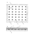
- FIG. 1A is a plan view
- FIG. 1B is a cross-sectional view taken along line A-A ′ in FIG.
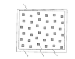
- the top view of the structure of the other transparent electrode which concerns on 1st embodiment of this invention is shown.
- the transparent electrode 1 of this embodiment is provided with the transparent base material 2, the metal layer 3, and the transparent conductive layer 5 which were arrange
- the surface resistivity of the conductive surface of the transparent electrode 1 is 0.01 ⁇ / ⁇ or more and 100 ⁇ / ⁇ or less. Preferably, it is 0.1 ⁇ / ⁇ or more and 10 ⁇ / ⁇ or less.
- the transparent electrode 1 of the present embodiment can be used for a transparent electrode 1 such as an LCD, an electroluminescence element, a plasma display, an electrochromic display, a solar battery, a touch panel, electronic paper, an electromagnetic wave shielding material, etc. It is preferable to use it for an organic EL element because of its excellent properties and high smoothness.
- the transparent base material 2 is comprised from a plastic film, a plastic plate, glass etc., for example.
- raw materials for plastic films and plastic plates include polyesters such as polyethylene terephthalate (PET) and polyethylene naphthalate, polyethylene (PE), polypropylene (PP), polystyrene, and ethylene-vinyl acetate copolymer resin (EVA).
- PET polyethylene terephthalate
- PE polyethylene
- PP polypropylene
- EVA ethylene-vinyl acetate copolymer resin
- Polyolefins polyvinyl resins such as polyvinyl chloride and polyvinylidene chloride, polyether ether ketone (PEEK), polysulfone (PSF), polyether sulfone (PES), polycarbonate (PC), polyamide, polyimide, acrylic resin, Triacetyl cellulose (TAC) or the like can be used.
- PEEK polyether ether ketone
- PSF polysulfone
- PES polyether sulfone
- PC polycarbonate
- polyamide polyimide
- acrylic resin Triacetyl cellulose (TAC) or the like
- TAC Triacetyl cellulose
- the transparent substrate 2 is preferably excellent in surface smoothness.
- the smoothness of the surface is preferably such that the arithmetic average roughness Ra is 5 nm or less and the maximum height Ry is 50 nm or less, more preferably the arithmetic average roughness Ra is 1 nm or less and Ry is 20 nm or less.
- the smoothness of the surface can be calculated from measurement using an atomic force microscope (AFM) or the like.
- the smoothness of the surface of the transparent substrate 2 may be smoothed by applying an undercoat layer such as a thermosetting resin, an ultraviolet curable resin, an electron beam curable resin, a radiation curable resin, or a machine such as polishing. It can be smoothed by processing.
- an undercoat layer such as a thermosetting resin, an ultraviolet curable resin, an electron beam curable resin, a radiation curable resin, or a machine such as polishing. It can be smoothed by processing.
- a gas barrier layer for the purpose of blocking oxygen and moisture in the atmosphere.
- metal oxide such as silicon oxide, silicon nitride, silicon oxynitride, aluminum nitride, aluminum oxide, or metal nitride can be used. These materials have an oxygen barrier function in addition to a water vapor barrier function.
- silicon nitride and silicon oxynitride having favorable barrier properties, solvent resistance, and transparency are preferable.
- the gas barrier layer can have a multi-layer structure as necessary. In that case, you may comprise only an inorganic layer and may comprise an inorganic layer and an organic layer.
- the gas barrier layer for example, a resistance heating vapor deposition method, an electron beam vapor deposition method, a reactive vapor deposition method, an ion plating method, or a sputtering method can be used depending on the material.
- the thickness of the gas barrier layer is not particularly limited, but typically it is preferably in the range of 5 nm to 500 nm per layer, more preferably 10 nm to 200 nm per layer.
- the gas barrier layer is provided on at least one surface of the transparent substrate 2 and is preferably provided on both surfaces.
- the metal layer 3 preferably has a low electric resistance, and a material having a conductivity of, for example, 10 7 S / cm or more is used.
- a material having a conductivity of, for example, 10 7 S / cm or more is used.
- a conductive material include metals such as aluminum, silver, chromium, gold, copper, tantalum, and molybdenum and / or alloys thereof.
- aluminum, chromium, copper, silver, and alloys thereof are preferable from the viewpoint of high conductivity and ease of material handling.
- the conductivity of the metal layer 3 may be equal to or higher than the conductivity of the transparent conductive layer 5 described later.
- the metal layer 3 of the present embodiment is configured by disposing the above-described conductive material at predetermined intervals in an island shape with respect to the surface of the transparent substrate 2.
- the arrangement condition is determined in consideration of the human visual limit. That is, from the relationship between spatial frequency and visual characteristics, when the viewing distance is 30 cm, the human eye cannot basically distinguish resolutions of 300 (84.7 ⁇ m) to 400 (63.5 ⁇ m) dpi or more. . For this reason, it is preferable that the size a of the island constituting the metal layer 3 is 100 ⁇ m or less as a condition that the metal layer 3 is not visually recognized.
- a size (size a) slightly larger than the visual limit range is selected.
- the plane figure of each island of the metal layer 3 is a polygon or a circle, any figure may be selected. However, it is preferable to select only one plane figure. This is because if two or more types of shapes exist adjacent to each other, the metal layer 3 may be easily visible.
- the plane figure of each island is preferably a symmetric figure shape with small anisotropy such as a regular polygon.
- the size a of the island is, for example, the length of the long side when the planar figure (planar shape) is a rectangular shape.
- the planar figure of the island is a polygonal shape, the longest length passing through the center of gravity is defined as the size a.
- the diameter is defined as a.
- the length in the direction perpendicular to the island arrangement direction on the side where the distance b between the islands is short may be defined as the island size a.
- the distance b between the islands that become the transmission region may be visually recognized.
- the visual distance since the visual distance may be closer than 30 cm, the interval slightly smaller than the visual limit is selected.
- the lower limit value of the island size a of the metal layer 3 is preferably 1 ⁇ m in consideration of technical accuracy in the process described later.
- each island of the metal layer 3 is set to 1 ⁇ m to 100 ⁇ m, and the arrangement interval b between the islands is selected within a range of 50 ⁇ m or more.
- interval b of islands is limited from the performance requested
- the height (thickness) of the metal layer 3 may be determined according to the desired conductivity, but is preferably 0.01 ⁇ m or more and 10 ⁇ m or less, and more preferably 0.1 ⁇ m or more and 1 ⁇ m or less.
- the metal layer 3 can also be made into a multilayer structure as needed. In that case, you may comprise only with the same electrically-conductive material, and you may comprise with a different electrically-conductive material.
- the light transmittance is reduced by arranging the metal layer 3, it is important that the reduction is as small as possible.
- the distance b between the islands is made too narrow or the size a of the island is set large. It is preferable that the light transmittance is 50% or more, more preferably 80% or more without being too much.
- the arrangement of the metal layer 3 may be freely arranged as long as the above conditions are included. However, as shown in FIG. 1, when arranged in an orderly manner, the metal layer 3 may be visually recognized in a linear shape depending on the size (size a) of islands, the arrangement interval b, and the viewing distance. For this reason, as shown in FIG. 2, a layout in which the metal layer 3 is more difficult to visually recognize may be selected by randomly arranging the metal layers 3.
- the transparent conductive layer 5 is formed by a coating method.
- the solution for forming the transparent conductive layer 5 includes a material that becomes the transparent conductive layer 5 and a solvent.
- the material of the transparent conductive layer 5 preferably contains a polymer compound exhibiting conductivity.
- the polymer compound may contain a dopant.
- the conductivity of the polymer compound is 10 ⁇ 5 or more and 10 5 S / cm or less, preferably 10 ⁇ 3 or more and 10 5 S / cm or less in terms of conductivity.
- the transparent conductive layer 5 consists of a high molecular compound which shows electroconductivity substantially.
- the transparent conductive layer 5 As a material constituting the transparent conductive layer 5, for example, polyaniline and derivatives thereof, polythiophene and derivatives thereof, and the like can be used.
- a known dopant can be used as the dopant, and examples thereof include organic sulfonic acids such as polystyrene sulfonic acid and dodecylbenzene sulfonic acid, and Lewis acids such as PF 5 , AsF 5 , and SbF 5 .
- the polymer compound exhibiting conductivity may be a self-doped polymer compound in which a dopant is directly bonded to the polymer compound.
- the transparent conductive layer 5 is preferably composed of polythiophene and derivatives thereof, and is substantially preferably composed of polythiophene and derivatives thereof.
- Polythiophene and its derivatives may contain a dopant. Since polythiophene, a polythiophene derivative, or a mixture of polythiophene and a polythiophene derivative is easily dissolved or dispersed in an aqueous solvent such as water and alcohol, it is preferably used as a solute of a coating solution used in a coating method. Moreover, these have high electroconductivity and are used suitably as an electrode material.
- these have a HOMO energy of about 5.0 eV, and the difference from the HOMO energy of an organic light emitting layer used in a normal organic EL element is as low as about 1 eV. Therefore, since holes can be efficiently injected into the organic light emitting layer, it can be suitably used particularly as a material for the anode. Moreover, these have high transparency and are suitably used as an electrode on the light emission extraction side of the organic EL element.
- the transparent conductive layer 5 is preferably composed of polyaniline and a derivative thereof, and is preferably substantially composed of polyaniline and a derivative thereof.
- Polyaniline and its derivatives may contain a dopant.
- Polyaniline and its derivatives are suitably used as electrode materials because they are excellent in conductivity and stability. Further, it has high transparency and is suitably used as an electrode on the light emission extraction side of the organic EL element.
- the film thickness may be determined according to the desired conductivity, but is preferably selected so that the transparent electrode 1 can obtain high smoothness.
- the transparent conductive layer 5 is preferably equal to or greater than the film thickness of the metal layer 3 as shown in FIG.
- the transparent electrode 1 is manufactured by forming a metal layer 3 and a transparent conductive layer 5 in this order on a transparent substrate 2. That is, the method for manufacturing the transparent electrode 1 includes a metal layer forming step for forming the metal layer 3 and a transparent conductive layer forming step for forming the transparent conductive layer 5.
- the method for forming the metal layer 3 is not particularly limited.
- the metal layer 3 may be formed from a constituent material of the metal layer 3 by a resistance heating vapor deposition method, an electron beam vapor deposition method, a sputtering method, or a laminating method in which a metal thin film is thermally compressed. After forming the film, it is possible to use a method of forming the aforementioned pattern by an etching method using a photoresist. Further, as a method for forming the metal layer 3, for example, film formation from a solution containing a material that becomes the metal layer 3 can be used.
- the solvent used for film formation from a solution is not particularly limited as long as it dissolves the material to be the metal layer 3.
- a film forming method from a solution for example, spin coating method, casting method, micro gravure coating method, gravure coating method, bar coating method, roll coating method, wire bar coating method, dip coating method, spray coating method, Application methods such as screen printing, flexographic printing, offset printing, slit coating, ink jet printing, and nozzle printing can be used.
- a film forming method capable of directly forming the pattern described above is preferable, and can be selected as appropriate.
- a printing method such as a screen printing method, a flexographic printing method, an offset printing method, an ink jet printing method, a nozzle printing method.
- a coating method by discharge such as a method is suitable. Thereafter, the metal layer 3 is formed by drying and solidifying.
- Transparent conductive layer forming process In the transparent conductive layer forming step, a solution containing the material of the transparent conductive layer 5 is applied to the transparent substrate 2 including the metal layer 3 over the entire surface of the transparent conductive layer forming region 4. Further, a solution containing a conductive material is applied to the transparent conductive layer forming region 4 to form a transparent conductive layer 5 (see FIG. 1A).
- the method for forming the transparent conductive layer 5 include spin coating, casting, micro gravure coating, gravure coating, bar coating, roll coating, wire bar coating, dip coating, spray coating, Application methods such as screen printing, flexographic printing, offset printing, slit coating, ink jet printing, and nozzle printing can be used.
- a uniform coating method is preferable and can be selected as appropriate.
- a spin coating method, a bar coating method, a wire bar coating method can be used.
- a coating method such as a dip coating method, a spray coating method, a slit coating method, a casting method, a micro gravure coating method, a gravure coating method, or a roll coating method is preferable.
- the transparent base material 2 in which a solution containing a conductive material is applied to the entire surface of the transparent conductive layer forming region 4 is heat-treated in a drying treatment chamber under a temperature condition of, for example, 100 ° C. Thereby, the solvent contained in the solution containing the conductive material is vaporized, and the conductive material is fixed on the transparent substrate 2 and the metal layer 3 to form the transparent conductive layer 5.
- the organic EL element in the present embodiment includes the transparent electrode 1 having the above-described configuration.
- the organic EL element can use the transparent electrode 1 as an anode, and the organic light emitting layer and the cathode can be made of any material and configuration generally used for the organic EL element.
- the element structure of the organic EL element for example, elements having various structures such as the following (A) to (E) can be used.
- A Anode / organic light emitting layer / cathode
- B anode / hole transport layer / organic light emitting layer / electron transport layer / cathode
- C anode / hole injection layer / hole transport layer / organic light emitting layer / electron transport Layer / cathode
- D anode / hole injection layer / organic light emitting layer / electron transport layer / electron injection layer / cathode
- E anode / hole injection layer / organic light emitting layer / electron injection layer / cathode
- the symbol “/” shown in A) to (E) indicates that the layers sandwiching the symbol “/” are stacked adjacent to each other. The same applies to the following description.
- the organic EL element may have a configuration having two or more organic light emitting layers.
- an organic EL element having two or more organic light emitting layers for example, the layer configuration shown in the following (F) can be used.
- an organic EL device having three or more organic light emitting layers specifically, (charge generation layer / charge injection layer / hole transport layer / organic light emission layer / electron transport layer / charge injection layer)
- a layer structure including two or more repeating units shown in (G) below can be used.
- the charge generation layer is a layer that generates holes and electrons by applying an electric field.
- a thin film made of vanadium oxide, ITO, molybdenum oxide, or the like can be used as the charge generation layer.
- a layer provided between the anode and the organic light emitting layer a hole injection layer, a hole transport layer, an organic light emitting layer, a layer provided between the cathode and the light emitting layer, an electron transport layer, an electron injection layer, and a cathode
- a layer provided between the cathode and the light emitting layer a layer provided between the cathode and the light emitting layer, an electron transport layer, an electron injection layer, and a cathode
- Examples of the layer provided between the cathode and the organic light emitting layer as needed include an electron injection layer, an electron transport layer, a hole blocking layer, and the like.
- the layer in contact with the cathode is called an electron injection layer, and the layers other than the electron injection layer are the electron transport layer. That's it.
- the electron injection layer is a layer having a function of improving electron injection efficiency from the cathode.
- the electron transport layer is a layer having a function of improving electron injection from the cathode, the electron injection layer, or a layer closer to the cathode.
- the hole blocking layer is a layer having a function of blocking hole transport. In the case where at least one of the electron injection layer and the electron transport layer has a function of blocking hole transport, these layers may also serve as the hole blocking layer.
- the hole injection layer can be provided between the anode and the hole transport layer, or between the anode and the organic light emitting layer.
- the material constituting the hole injection layer (hole injection material)
- a known material can be used as appropriate, and there is no particular limitation. Therefore, examples of the hole injection material include phenylamine, starburst amine, phthalocyanine, hydrazone derivative, carbazole derivative, triazole derivative, imidazole derivative, oxadiazole derivative having amino group, vanadium oxide, tantalum oxide. Further, oxides such as molybdenum oxide, amorphous carbon, polyaniline, polythiophene derivatives, and the like can be used.
- a film formation method of the hole injection layer for example, film formation from a solution containing a hole injection material can be used.
- the solvent used for film formation from a solution is not particularly limited as long as it dissolves the hole injection material, for example, a chlorine-based solvent such as chloroform, methylene chloride, dichloroethane, an ether-based solvent such as tetrahydrofuran, Aromatic hydrocarbon solvents such as toluene and xylene, ketone solvents such as acetone and methyl ethyl ketone, ester solvents such as ethyl acetate, butyl acetate and ethyl cellosolve acetate, and water can be used.
- a chlorine-based solvent such as chloroform, methylene chloride, dichloroethane
- an ether-based solvent such as tetrahydrofuran
- Aromatic hydrocarbon solvents such as toluene and xylene
- Examples of film forming methods from solutions include spin coating, casting, micro gravure coating, gravure coating, bar coating, roll coating, wire bar coating, dip coating, spray coating, and screen printing. It is possible to use coating methods such as a printing method, a flexographic printing method, an offset printing method, a slit coating method, an ink jet printing method, and a nozzle printing method.
- the thickness of the hole injection layer is preferably in the range of 5 nm to 300 nm. This is because manufacturing tends to be difficult when the thickness of the hole injection layer is less than 5 nm. On the other hand, if the thickness of the hole injection layer exceeds 300 nm, the driving voltage and the voltage applied to the hole injection layer tend to increase.
- the material constituting the hole transport layer is not particularly limited.
- N, N′-diphenyl-N, N′-di (3-methylphenyl) 4,4′-diamino Aromatic amine derivatives such as biphenyl (TPD), 4,4′-bis [N- (1-naphthyl) -N-phenylamino] biphenyl (NPB), polyvinylcarbazole or derivatives thereof, polysilane or derivatives thereof, side chain or Polysiloxane derivative having aromatic amine in the main chain, pyrazoline derivative, arylamine derivative, stilbene derivative, triphenyldiamine derivative, polyaniline or derivative thereof, polythiophene or derivative thereof, polyarylamine or derivative thereof, polypyrrole or derivative thereof, poly (P-phenylene vinylene) or derivatives thereof, poly (2, 5-thienylene vinylene) or a derivative thereof can be used.
- hole transport material among the materials described above, polyvinyl carbazole or a derivative thereof, polysilane or a derivative thereof, a polysiloxane derivative having an aromatic amine in a side chain or a main chain, a polyaniline, or a derivative thereof, polythiophene or a derivative thereof
- Polymer hole transport materials such as polyarylamine or derivatives thereof, poly (p-phenylene vinylene) or derivatives thereof, poly (2,5-thienylene vinylene) or derivatives thereof are preferred.
- a low-molecular hole transport material it is preferably used by being dispersed in a polymer binder.
- the method for forming the hole transport layer is not particularly limited, but in the case of a low-molecular hole transport material, it is possible to use film formation from a mixed liquid containing a polymer binder and a hole transport material. .
- film formation from a solution containing a hole transport material can be used.
- the solvent used for film formation from a solution is not particularly limited as long as it can dissolve a hole transport material, and the solvent exemplified in the section of the hole injection layer can be used as an example. It is.
- a film formation method from a solution a coating method similar to the above-described film formation method of the hole injection layer can be used.
- the thickness of the hole transport layer is not particularly limited, but can be appropriately changed according to the intended design, and is preferably in the range of 1 nm to 1000 nm, for example. This is because when the thickness of the hole transport layer is less than 1 nm, production tends to be difficult and the effect of hole transport cannot be obtained sufficiently. On the other hand, when the thickness of the hole transport layer exceeds 1000 nm, the driving voltage and the voltage applied to the hole transport layer tend to increase. Therefore, the thickness of the hole transport layer is preferably in the range of 1 nm to 1000 nm, more preferably in the range of 2 nm to 500 nm, and still more preferably in the range of 5 nm to 200 nm. It is.
- the organic light emitting layer has an organic substance (a low molecular compound and a high molecular compound) that mainly emits fluorescence or phosphorescence.
- the organic light emitting layer may further contain a dopant material.
- a material for forming the organic light emitting layer for example, the following materials can be used.
- the dye-based materials include cyclopentamine derivatives, quinacudrine derivatives, coumarin derivatives, tetraphenylbutadiene derivative compounds, triphenylamine derivatives, oxadiazole derivatives, pyrazoloquinoline derivatives, distyrylbenzene derivatives, diesters.
- a styrylarylene derivative, pyrrole derivative, thiophene ring compound, pyridine ring compound, perinone derivative, perylene derivative, oligothiophene derivative, oxadiazole dimer, pyrazoline dimer, or the like can be used.
- Metal complex materials examples include metal complexes that emit light from triplet excited states such as iridium complexes and platinum complexes, aluminum quinolinol complexes, benzoquinolinol beryllium complexes, benzoxazolyl zinc complexes, and benzo Thiazole zinc complex, azomethyl zinc complex, porphyrin zinc complex, europium complex, etc., the central metal having a rare earth metal such as Al, Zn, Be, or Tb, Eu, Dy, etc., and oxadiazole as the ligand, A metal complex having thiadiazole, phenylpyridine, phenylbenzimidazole, quinoline structure, or the like can be used.
- metal complexes that emit light from triplet excited states such as iridium complexes and platinum complexes, aluminum quinolinol complexes, benzoquinolinol beryllium complexes, benzoxazolyl zinc complexes, and benzo Thiazole zinc complex,
- polymeric materials include polyparaphenylene vinylene derivatives, polythiophene derivatives, polyparaphenylene derivatives, polysilane derivatives, polyacetylene derivatives, polyfluorene derivatives, polyvinyl carbazole derivatives, the above-mentioned dye bodies and metal complex luminescence. It is possible to use a polymerized material.
- a distyrylarylene derivative, an oxadiazole derivative and a polymer thereof a polyvinylcarbazole derivative, a polyparaphenylene derivative, a polyfluorene derivative, or the like can be used as a material that emits blue light.
- a distyrylarylene derivative, an oxadiazole derivative and a polymer thereof a polyvinylcarbazole derivative, a polyparaphenylene derivative, a polyfluorene derivative, or the like can be used. Is possible.
- a material that emits green light for example, a quinacrine derivative, a coumarin derivative and a polymer thereof
- a polyparaphenylene vinylene derivative, a polyfluorene derivative, or the like can be used as a material that emits green light.
- a material that emits red light for example, a coumarin derivative, a thiophene ring compound and a polymer thereof
- a polyparaphenylene vinylene derivative, a polythiophene derivative, a polyfluorene derivative, or the like can be used. It is.
- a dopant in an organic light emitting layer for the purpose of improving luminous efficiency or changing the emission wavelength.
- a dopant for example, a perylene derivative, a coumarin derivative, a rubrene derivative, a quinacdrine derivative, a squalium derivative, a porphyrin derivative, a styryl dye, a tetracene derivative, a pyrazolone derivative, decacyclene, phenoxazone, and the like can be used.
- the thickness of the organic light emitting layer is usually in the range of about 2 nm to 200 nm.
- the organic light emitting layer As a method for forming the organic light emitting layer, it is possible to use film formation from a solution containing a material constituting the organic light emitting layer (organic light emitting material). Further, the solvent used for film formation from a solution is not particularly limited as long as it dissolves an organic light emitting material, and the solvent exemplified in the section of the hole injection layer can be used as an example. is there. In addition, as a film formation method from a solution, a coating method similar to the above-described film formation method of the hole injection layer can be used.
- Examples of the layer provided between the cathode and the organic light emitting layer as needed include an electron injection layer, an electron transport layer, a hole blocking layer, and the like.
- an electron injection layer is a layer in contact with the cathode
- a layer excluding this electron injection layer is referred to as an electron transport layer.
- the electron injection layer is a layer having a function of improving electron injection efficiency from the cathode.
- the electron transport layer is a layer having a function of improving electron injection from the cathode, the electron injection layer, or a layer closer to the cathode.
- the hole blocking layer is a layer having a function of blocking hole transport. When at least one of the electron injection layer and the electron transport layer has a function of blocking hole transport, these layers may also serve as a hole blocking layer.
- Electrode transport layer As a material constituting the electron transport layer (electron transport material), a known material can be used, for example, an oxadiazole derivative, anthraquinodimethane or a derivative thereof, benzoquinone or a derivative thereof, naphthoquinone or a derivative thereof.
- Anthraquinone or derivatives thereof, tetracyanoanthraquinodimethane or derivatives thereof, fluorenone or derivatives thereof, diphenyldicyanoethylene or derivatives thereof, diphenoquinone derivatives, metal complexes of 8-hydroxyquinoline or derivatives thereof, polyquinoline or derivatives thereof, polyquinoxaline or A derivative thereof, polyfluorene, a derivative thereof, or the like can be used.
- examples of the electron transport material include oxadiazole derivatives, benzoquinone or derivatives thereof, anthraquinones or derivatives thereof, metal complexes of 8-hydroxyquinoline or derivatives thereof, polyquinoline or derivatives thereof, polyquinoxaline or derivatives thereof, poly Fluorene or its derivatives are preferred, and 2- (4-biphenylyl) -5- (4-tert-butylphenyl) -1,3,4-oxadiazole, benzoquinone, anthraquinone, tris (8-quinolinol) aluminum, polyquinoline are preferred. Further preferred.
- the method for forming the electron transport layer is not particularly limited, but for a low-molecular electron transport material, it is possible to use a film formed from a mixed solution containing a polymer binder and an electron transport material.
- a polymer electron transport material film formation from a solution containing an electron transport material can be used.
- the solvent used for film formation from a solution is not particularly limited as long as it dissolves an electron transport material, and the solvent exemplified in the section of the hole injection layer can be used as an example.
- a film formation method from a solution a coating method similar to the above-described film formation method of the hole injection layer can be used.
- the film thickness of the electron transport layer varies depending on the material used and can be changed as appropriate according to the intended design. However, at least a film thickness that does not cause pinholes is required. Therefore, the thickness of the electron transport layer is preferably, for example, in the range of 1 nm to 1000 nm, more preferably in the range of 2 nm to 500 nm, and still more preferably in the range of 5 nm to 200 nm. Within range.
- an optimal material is appropriately selected according to the type of the organic light emitting layer, and includes, for example, at least one of alkali metal, alkaline earth metal, alkali metal, and alkaline earth metal.
- An alloy, an alkali metal or alkaline earth metal oxide, halide, carbonate, or a mixture of these substances can be used.
- alkali metal, alkali metal oxide, halide and carbonate examples include lithium, sodium, potassium, rubidium, cesium, lithium oxide, lithium fluoride, sodium oxide, sodium fluoride, potassium oxide, potassium fluoride, Rubidium oxide, rubudium fluoride, cesium oxide, cesium fluoride, lithium carbonate, or the like can be used.
- the alkaline earth metal, alkaline earth metal oxide, halide and carbonate include, for example, magnesium, calcium, barium, strontium, magnesium oxide, magnesium fluoride, calcium oxide, calcium fluoride, barium oxide, Barium fluoride, strontium oxide, strontium fluoride, magnesium carbonate, or the like can be used.
- the electron injection layer may be formed of a stacked body in which two or more layers are stacked. In this case, as a material constituting the electron injection layer, for example, lithium fluoride / calcium can be used.
- the electron injection layer is formed by various vapor deposition methods, sputtering methods, various coating methods, and the like.
- the thickness of the electron injection layer is preferably in the range of 1 nm to 1000 nm.
- cathode As a material for the cathode, it is preferable to use at least one material among a material having a small work function and easy electron injection into the organic light emitting layer, a material having a high conductivity, and a material having a high visible light reflectance.
- a material for the cathode for example, a metal, a metal oxide, an alloy, graphite, a graphite intercalation compound, an inorganic semiconductor such as zinc oxide, or the like can be used.
- the metal used as the cathode material for example, alkali metals, alkaline earth metals, transition metals, III-b group metals, and the like can be used.
- these metals include lithium, sodium, potassium, rubidium, cesium, beryllium, magnesium, calcium, strontium, barium, gold, silver, platinum, copper, manganese, titanium, cobalt, nickel, tungsten, tin , Aluminum, scandium, vanadium, zinc, yttrium, indium, cerium, samarium, europium, terbium, ytterbium, and the like.
- an alloy used as a material for the cathode an alloy containing at least one of the above metals can be used.
- magnesium-silver alloy, magnesium-indium alloy, magnesium-aluminum alloy, indium-silver alloy, lithium-aluminum alloy, lithium-magnesium alloy, lithium-indium alloy, calcium-aluminum alloy, etc. can be used. It is.
- the cathode is used as the transparent electrode 1 as necessary.
- the material include conductive oxides such as indium oxide, zinc oxide, tin oxide, ITO, and IZO, polyaniline or a derivative thereof, polythiophene or a component thereof. It is possible to use a conductive organic material such as a derivative.
- the cathode may have a laminated structure of two or more layers. Moreover, you may use an electron injection layer as a cathode.
- the film thickness of the cathode can be appropriately selected in consideration of conductivity and durability, but is, for example, in the range of 10 nm to 10000 nm, preferably in the range of 20 nm to 1000 nm, More preferably, it exists in the range of 50 nm or more and 500 nm or less.
- the organic EL element of this embodiment can be used for, for example, a self-luminous display, a liquid crystal backlight, illumination, and the like.
- the transparent electrode 1 has a size a of each island a in the metal layer 3 in consideration of human visual limitations when the metal layer 3 is arranged in an island shape. Is selected from the range of 1 ⁇ m or more and 100 ⁇ m or less and the disposition interval b between the islands is 50 ⁇ m or more. According to this configuration, the size “a” and the interval “b” of the islands forming the metal layer 3 are selected in a range that takes into account the human visual limit. Furthermore, the transparent conductive layer 5 is formed on the transparent base material 2 so as to cover the metal layer 3, and visibility is improved.
- the transparent electrode 1 in which the metal layer 3 is not visually recognized and has a low resistance For example, when combined with an organic EL element, the appearance of light emission is not hindered by the metal layer 3 and defects such as light emission unevenness. No light emitting element is obtained.
- each island of the metal layer 3 may be in the range of 10 nm to 1 ⁇ m.
- the plane figure of each island of the metal layer 3 may be limited to any one of a polygon and a circle.
- the arrangement of the islands of the metal layer 3 may be random.
- the conductivity of the metal layer 3 may be set to be equal to or lower than the conductivity of the transparent conductive layer 5. With this configuration, it becomes possible to efficiently apply a voltage to the organic light emitting layer sandwiched between the transparent electrode 1 (anode) and the counter electrode (cathode), and the efficiency of light emission from the organic light emitting layer can be improved. Can be increased.
- the transparent electrode 1 may have a light transmittance of 50% or more. With this configuration, the amount of light required when using the transparent electrode 1 can be reliably obtained. As mentioned above, although embodiment of this invention was explained in full detail, actually, it is not restricted to the said embodiment, Even if there is a change of the range which does not deviate from the summary of this invention, it is included in this invention.
Abstract
Provided are a transparent electrode with which it is possible to solve the problem of the external appearance being impeded by a metal layer, and an organic EL element provided with the transparent electrode. A transparent electrode (1) according to the present embodiment has: a transparent substrate (2); a metal layer (3) arranged on the transparent substrate (2) such that gaps (b) are opened to form islands, the metal layer (3) being formed such that the size of each of the islands is within a range of 1-100 μm; and a transparent conductor layer (5) formed on the transparent substrate (2) so as to cover the metal layer (3). An organic electroluminescence element, provided with the transparent electrode (1).
Description
本発明は、透明電極、及び透明電極を備えた有機エレクトロルミネッセンス素子に関する。
The present invention relates to a transparent electrode and an organic electroluminescence element provided with the transparent electrode.
近年、液晶表示素子(Liquid Crystal Display:LCD)に続く次世代表示デバイスとして、有機エレクトロルミネッセンス素子(以下、「有機EL素子」とも呼称する)等、自発光素子を二次元配列した発光素子型の表示パネルを備えた発光素子の研究開発が行われている。
有機EL素子は、陽極と、陰極と、これらの一対の電極間に形成される有機EL層(発光機能層)とを備える。この有機EL層は、例えば、有機発光層、正孔注入層等を有する。そして、有機EL素子は、有機EL層中の有機発光層において正孔と電子が再結合することによって発生するエネルギーにより発光する。 In recent years, as a next-generation display device following a liquid crystal display (LCD), a light-emitting element type in which self-light-emitting elements such as organic electroluminescence elements (hereinafter also referred to as “organic EL elements”) are two-dimensionally arranged. Research and development of light-emitting elements including a display panel are being conducted.
The organic EL element includes an anode, a cathode, and an organic EL layer (light emitting functional layer) formed between the pair of electrodes. This organic EL layer has, for example, an organic light emitting layer, a hole injection layer, and the like. The organic EL element emits light by energy generated by recombination of holes and electrons in the organic light emitting layer in the organic EL layer.
このような有機EL素子の光を取り出す側の透明電極としては、一般には、錫ドープ酸化インジウム(Indium Thin Oxide:ITO)や、亜鉛ドープ酸化インジウム(Indium Zinc Oxide:IZO)等を用いて形成される。しかし、この透明電極は、低抵抗を得るためには、厚く均一な膜を形成しなければならない。このため、光透過率の減少、価格の高騰、形成プロセスにおける高温処理の手間等が発生するため、特に、フィルム上での低抵抗化には限界があった(例えば、特許文献1を参照)。
The transparent electrode on the light extraction side of such an organic EL element is generally formed using tin-doped indium oxide (Indium Thin Oxide: ITO), zinc-doped indium oxide (Indium Zinc Oxide: IZO), or the like. The However, in order to obtain a low resistance, this transparent electrode must form a thick and uniform film. For this reason, a decrease in light transmittance, an increase in price, a labor for high-temperature treatment in the formation process, and the like occur, and there is a limit to reducing the resistance on the film in particular (see, for example, Patent Document 1). .
そのため、近年では、ITOを用いない透明電極の技術が開示されている。例えば、一様な網目状、櫛形、または、グリッド型等の金属及び合金のうち少なくとも一方の細線構造部を配置した導電性面を作製し、その上に、例えば、導電性高分子材料を適当な溶媒に溶解または分散したインクを、塗布法や印刷法を用いて透明導電層を形成することによって、低抵抗な透明電極を形成する方法が提案されている(例えば、特許文献2や特許文献3を参照)。
Therefore, in recent years, transparent electrode technology that does not use ITO has been disclosed. For example, a conductive surface in which at least one fine wire structure portion of a uniform mesh shape, comb shape, or grid type metal and alloy is arranged is prepared, and a conductive polymer material is appropriately formed thereon, for example. A method of forming a transparent electrode having a low resistance by forming a transparent conductive layer using an ink dissolved or dispersed in an appropriate solvent using a coating method or a printing method has been proposed (for example, Patent Document 2 and Patent Document 2). 3).
ところで、上述する細線構造を有した金属層と透明導電層を組み合わせてなる透明電極を採用した有機EL素子は、金属層の大きさや形状によっては、金属細線が視認され易く、外観を阻害する恐れがある。
本発明は、このような問題を解決しようとするものであり、金属層により阻害される外観を解決可能な透明電極、及びその透明電極を備えた有機EL素子を提供することを目的としている。 By the way, the organic EL element which employs the transparent electrode formed by combining the metal layer having the thin wire structure and the transparent conductive layer described above may easily see the metal thin wire depending on the size and shape of the metal layer, and may impair the appearance. There is.
The present invention is intended to solve such problems, and an object thereof is to provide a transparent electrode capable of solving the appearance that is hindered by a metal layer, and an organic EL device including the transparent electrode.
課題を解決するために、本発明の一態様である透明電極は、透明基材と、前記透明基材上に、間隔を開けて配置された複数の島から構成されると共に各島の幅が1μm以上100μm以下の金属層と、前記金属層を覆うように前記透明基材上に形成された透明導電層と、を有することを特徴とする。
また、本発明の一態様である有機エレクトロルミネッセンス素子は、本発明の一態様である透明電極を備えることを特徴とする。 In order to solve the problem, a transparent electrode which is one embodiment of the present invention is composed of a transparent base material and a plurality of islands arranged at intervals on the transparent base material, and the width of each island is It has a 1 to 100 micrometer metal layer, and the transparent conductive layer formed on the said transparent base material so that the said metal layer may be covered, It is characterized by the above-mentioned.
An organic electroluminescent element which is one embodiment of the present invention includes a transparent electrode which is one embodiment of the present invention.
本発明においては、金属層を島状の配置構造とし、さらにその各島の大きさを人間の視覚限界を考慮した範囲で選択することで、外観を改善することが可能となる。
In the present invention, the appearance of the metal layer can be improved by making the metal layer into an island-like arrangement structure and further selecting the size of each island within a range that takes into consideration the human visual limit.
以下、この発明の実施形態について図面を参照して説明する。
ここで、図面は模式的なものであり、厚みと平面寸法との関係、各層の厚みの比率等は現実のものとは異なる。また、以下に示す実施形態は、本発明の技術的思想を具体化するための構成を例示するものであって、本発明の技術的思想は、構成部品の材質、形状、構造等が下記のものに特定するものでない。本発明の技術的思想は、請求の範囲に記載された請求項が規定する技術的範囲内において、種々の変更を加えることができる。 Embodiments of the present invention will be described below with reference to the drawings.
Here, the drawings are schematic, and the relationship between the thickness and the planar dimensions, the ratio of the thickness of each layer, and the like are different from the actual ones. Further, the embodiment described below exemplifies a configuration for embodying the technical idea of the present invention, and the technical idea of the present invention is that the material, shape, structure, etc. of the component parts are as follows. It is not something specific. The technical idea of the present invention can be variously modified within the technical scope defined by the claims described in the claims.
<透明電極1の構成>
本実施形態の透明電極1は、図1に示すように、透明基材2と、島状に配置された金属層3と透明導電層5とを備えている。
本実施形態の透明電極1は、有機EL素子に用いた場合に輝度を向上させる観点から、透明電極1の導電性面の表面抵抗率は0.01Ω/□以上100Ω/□以下であることが好ましく、さらに好ましくは0.1Ω/□以上10Ω/□以下である。
本実施形態の透明電極1は、LCD、エレクトロルミネッセンス素子、プラズマディスプレイ、エレクトロクロミックディスプレイ、太陽電池、タッチパネルなどの透明電極1、電子ペーパーならびに電磁波遮蔽材などに用いることが出来るが、導電性、透明性に優れ、また平滑性も高いため、有機EL素子に用いることが好ましい。 <Configuration oftransparent electrode 1>
Thetransparent electrode 1 of this embodiment is provided with the transparent base material 2, the metal layer 3, and the transparent conductive layer 5 which were arrange | positioned at island shape, as shown in FIG.
From the viewpoint of improving luminance when thetransparent electrode 1 of this embodiment is used in an organic EL element, the surface resistivity of the conductive surface of the transparent electrode 1 is 0.01Ω / □ or more and 100Ω / □ or less. Preferably, it is 0.1Ω / □ or more and 10Ω / □ or less.
Thetransparent electrode 1 of the present embodiment can be used for a transparent electrode 1 such as an LCD, an electroluminescence element, a plasma display, an electrochromic display, a solar battery, a touch panel, electronic paper, an electromagnetic wave shielding material, etc. It is preferable to use it for an organic EL element because of its excellent properties and high smoothness.
本実施形態の透明電極1は、図1に示すように、透明基材2と、島状に配置された金属層3と透明導電層5とを備えている。
本実施形態の透明電極1は、有機EL素子に用いた場合に輝度を向上させる観点から、透明電極1の導電性面の表面抵抗率は0.01Ω/□以上100Ω/□以下であることが好ましく、さらに好ましくは0.1Ω/□以上10Ω/□以下である。
本実施形態の透明電極1は、LCD、エレクトロルミネッセンス素子、プラズマディスプレイ、エレクトロクロミックディスプレイ、太陽電池、タッチパネルなどの透明電極1、電子ペーパーならびに電磁波遮蔽材などに用いることが出来るが、導電性、透明性に優れ、また平滑性も高いため、有機EL素子に用いることが好ましい。 <Configuration of
The
From the viewpoint of improving luminance when the
The
(透明基材2)
透明基材2は、例えば、プラスチックフィルム、プラスチック板、ガラスなどから構成される。
プラスチックフィルム及びプラスチック板の原料としては、例えば、ポリエチレンテレフタラート(PET)、ポリエチレンナフタレートなどのポリエステル類、ポリエチレン(PE)、ポリプロピレン(PP)、ポリスチレン、エチレン-酢酸ビニル共重合樹脂(EVA)などのポリオレフィン類、ポリ塩化ビニル、ポリ塩化ビニリデンなどのビニル系樹脂、ポリエーテルエーテルケトン(PEEK)、ポリサルホン(PSF)、ポリエーテルサルホン(PES)、ポリカーボネート(PC)、ポリアミド、ポリイミド、アクリル樹脂、トリアセチルセルロース(TAC)などを用いることができる。 (Transparent substrate 2)
Thetransparent base material 2 is comprised from a plastic film, a plastic plate, glass etc., for example.
Examples of raw materials for plastic films and plastic plates include polyesters such as polyethylene terephthalate (PET) and polyethylene naphthalate, polyethylene (PE), polypropylene (PP), polystyrene, and ethylene-vinyl acetate copolymer resin (EVA). Polyolefins, polyvinyl resins such as polyvinyl chloride and polyvinylidene chloride, polyether ether ketone (PEEK), polysulfone (PSF), polyether sulfone (PES), polycarbonate (PC), polyamide, polyimide, acrylic resin, Triacetyl cellulose (TAC) or the like can be used.
透明基材2は、例えば、プラスチックフィルム、プラスチック板、ガラスなどから構成される。
プラスチックフィルム及びプラスチック板の原料としては、例えば、ポリエチレンテレフタラート(PET)、ポリエチレンナフタレートなどのポリエステル類、ポリエチレン(PE)、ポリプロピレン(PP)、ポリスチレン、エチレン-酢酸ビニル共重合樹脂(EVA)などのポリオレフィン類、ポリ塩化ビニル、ポリ塩化ビニリデンなどのビニル系樹脂、ポリエーテルエーテルケトン(PEEK)、ポリサルホン(PSF)、ポリエーテルサルホン(PES)、ポリカーボネート(PC)、ポリアミド、ポリイミド、アクリル樹脂、トリアセチルセルロース(TAC)などを用いることができる。 (Transparent substrate 2)
The
Examples of raw materials for plastic films and plastic plates include polyesters such as polyethylene terephthalate (PET) and polyethylene naphthalate, polyethylene (PE), polypropylene (PP), polystyrene, and ethylene-vinyl acetate copolymer resin (EVA). Polyolefins, polyvinyl resins such as polyvinyl chloride and polyvinylidene chloride, polyether ether ketone (PEEK), polysulfone (PSF), polyether sulfone (PES), polycarbonate (PC), polyamide, polyimide, acrylic resin, Triacetyl cellulose (TAC) or the like can be used.
透明基材2は、表面平滑性に優れているものが好ましい。その表面の平滑性は、算術平均粗さRaが5nm以下且つ最大高さRyが50nm以下であることが好ましく、さらに好ましくは算術平均粗さRaが1nm以下かつRyが20nm以下である。ここで、表面の平滑性は、原子間力顕微鏡(AFM)等による測定から算出することができる。
透明基材2の表面の平滑性は、熱硬化性樹脂、紫外線硬化性樹脂、電子線硬化性樹脂、放射線硬化性樹脂等の下塗り層を付与して平滑化してもよいし、研磨などの機械加工によって平滑にすることもできる。また、高分子層の塗布、接着性を向上させるため、コロナ、プラズマ、UV/オゾンによる表面処理をしてもよい。 Thetransparent substrate 2 is preferably excellent in surface smoothness. The smoothness of the surface is preferably such that the arithmetic average roughness Ra is 5 nm or less and the maximum height Ry is 50 nm or less, more preferably the arithmetic average roughness Ra is 1 nm or less and Ry is 20 nm or less. Here, the smoothness of the surface can be calculated from measurement using an atomic force microscope (AFM) or the like.
The smoothness of the surface of thetransparent substrate 2 may be smoothed by applying an undercoat layer such as a thermosetting resin, an ultraviolet curable resin, an electron beam curable resin, a radiation curable resin, or a machine such as polishing. It can be smoothed by processing. Moreover, in order to improve application | coating of a polymer layer and adhesiveness, you may surface-treat by corona, plasma, and UV / ozone.
透明基材2の表面の平滑性は、熱硬化性樹脂、紫外線硬化性樹脂、電子線硬化性樹脂、放射線硬化性樹脂等の下塗り層を付与して平滑化してもよいし、研磨などの機械加工によって平滑にすることもできる。また、高分子層の塗布、接着性を向上させるため、コロナ、プラズマ、UV/オゾンによる表面処理をしてもよい。 The
The smoothness of the surface of the
また、大気中の酸素、水分を遮断する目的でガスバリア層を設けるのが好ましい。ガスバリア層の形成材料としては、例えば、酸化シリコン、窒化シリコン、酸化窒化シリコン、窒化アルミニウム、酸化アルミニウム等の金属酸化物、金属窒化物が使用できる。これらの材料は、水蒸気バリア機能のほかに酸素バリア機能も有する。特に、バリア性、耐溶剤性、透明性が良好な窒化シリコン、酸化窒化シリコンが好ましい。また、ガスバリア層は必要に応じて多層構成にすることも可能である。その場合、無機層のみで構成してもよいし、無機層と有機層で構成してもよい。ガスバリア層の形成方法は、材料に応じて、例えば、抵抗加熱蒸着法、電子ビーム蒸着法、反応性蒸着法、イオンプレーティング法、スパッタリング法を用いることができる。また、ガスバリア層の厚さに関しては特に限定されないが、典型的には1層あたり5nm以上500nm以下の範囲内であることが好ましく、さらに好ましくは1層あたり10nm以上200nm以下である。ガスバリア層は透明基材2の少なくとも一方の面に設けられ、両面に設けられるのが好ましい。
It is also preferable to provide a gas barrier layer for the purpose of blocking oxygen and moisture in the atmosphere. As a material for forming the gas barrier layer, for example, metal oxide such as silicon oxide, silicon nitride, silicon oxynitride, aluminum nitride, aluminum oxide, or metal nitride can be used. These materials have an oxygen barrier function in addition to a water vapor barrier function. In particular, silicon nitride and silicon oxynitride having favorable barrier properties, solvent resistance, and transparency are preferable. Further, the gas barrier layer can have a multi-layer structure as necessary. In that case, you may comprise only an inorganic layer and may comprise an inorganic layer and an organic layer. As a method for forming the gas barrier layer, for example, a resistance heating vapor deposition method, an electron beam vapor deposition method, a reactive vapor deposition method, an ion plating method, or a sputtering method can be used depending on the material. Further, the thickness of the gas barrier layer is not particularly limited, but typically it is preferably in the range of 5 nm to 500 nm per layer, more preferably 10 nm to 200 nm per layer. The gas barrier layer is provided on at least one surface of the transparent substrate 2 and is preferably provided on both surfaces.
(金属層3)
金属層3としては、電気抵抗が低いことが好ましく、その材料は例えば107S/cm以上の導電率を有する材料が使用される。かかる導電材料の具体例としては、アルミニウム、銀、クロミウム、金、銅、タンタル、モリブデン等の金属および/またはその合金を挙げることができる。これらの中でも、導電率の高さ、および材料のハンドリングの容易さの観点から、アルミニウム、クロミウム、銅、銀およびその合金が好ましい。また、金属層3の導電率は、後述する透明導電層5の導電率以上であってもよい。 (Metal layer 3)
Themetal layer 3 preferably has a low electric resistance, and a material having a conductivity of, for example, 10 7 S / cm or more is used. Specific examples of such a conductive material include metals such as aluminum, silver, chromium, gold, copper, tantalum, and molybdenum and / or alloys thereof. Among these, aluminum, chromium, copper, silver, and alloys thereof are preferable from the viewpoint of high conductivity and ease of material handling. Further, the conductivity of the metal layer 3 may be equal to or higher than the conductivity of the transparent conductive layer 5 described later.
金属層3としては、電気抵抗が低いことが好ましく、その材料は例えば107S/cm以上の導電率を有する材料が使用される。かかる導電材料の具体例としては、アルミニウム、銀、クロミウム、金、銅、タンタル、モリブデン等の金属および/またはその合金を挙げることができる。これらの中でも、導電率の高さ、および材料のハンドリングの容易さの観点から、アルミニウム、クロミウム、銅、銀およびその合金が好ましい。また、金属層3の導電率は、後述する透明導電層5の導電率以上であってもよい。 (Metal layer 3)
The
本実施形態の金属層3は、上述の導電材料を、透明基材2の表面に対して島状に所定間隔を開けて配置することで構成する。
配置条件としては、人間の視覚限界を考慮させて決定する。
すなわち、空間周波数と視覚特性の関係から、視認距離が30cmの場合に、人間の目は基本的に300(84.7μm)~400(63.5μm)dpi以上の解像度を区別できないとされている。このため、金属層3が視認されない条件として、金属層3を構成する島の大きさaが100μm以下を選択することが好ましい。ここで、視認距離は30cmより遠い場合もあるため、前記視覚限界の範囲よりやや大きめのサイズ(大きさa)を選択している。 Themetal layer 3 of the present embodiment is configured by disposing the above-described conductive material at predetermined intervals in an island shape with respect to the surface of the transparent substrate 2.
The arrangement condition is determined in consideration of the human visual limit.
That is, from the relationship between spatial frequency and visual characteristics, when the viewing distance is 30 cm, the human eye cannot basically distinguish resolutions of 300 (84.7 μm) to 400 (63.5 μm) dpi or more. . For this reason, it is preferable that the size a of the island constituting themetal layer 3 is 100 μm or less as a condition that the metal layer 3 is not visually recognized. Here, since the visual recognition distance may be longer than 30 cm, a size (size a) slightly larger than the visual limit range is selected.
配置条件としては、人間の視覚限界を考慮させて決定する。
すなわち、空間周波数と視覚特性の関係から、視認距離が30cmの場合に、人間の目は基本的に300(84.7μm)~400(63.5μm)dpi以上の解像度を区別できないとされている。このため、金属層3が視認されない条件として、金属層3を構成する島の大きさaが100μm以下を選択することが好ましい。ここで、視認距離は30cmより遠い場合もあるため、前記視覚限界の範囲よりやや大きめのサイズ(大きさa)を選択している。 The
The arrangement condition is determined in consideration of the human visual limit.
That is, from the relationship between spatial frequency and visual characteristics, when the viewing distance is 30 cm, the human eye cannot basically distinguish resolutions of 300 (84.7 μm) to 400 (63.5 μm) dpi or more. . For this reason, it is preferable that the size a of the island constituting the
金属層3の各島の平面図形は、多角形または円形であれば、いずれの図形を選択しても構わない。但し、選択する平面図形はひとつに限定することが好ましい。これは2種類以上の形が隣接して存在すると、金属層3が視認されやすくなる恐れがあるためである。また、各島の平面図形は、正多角形などの異方性が小さい対称な図形形状が好ましい。
ここで、島の大きさaとは、例えば、平面図形(平面形状)が長方形形状の場合には、長辺の長さとする。島の平面図形が多角形形状の場合、その重心点を通り一番長い長さを大きさaとする。また島の平面図形が円形の場合には、その直径を大きさaとする。 As long as the plane figure of each island of themetal layer 3 is a polygon or a circle, any figure may be selected. However, it is preferable to select only one plane figure. This is because if two or more types of shapes exist adjacent to each other, the metal layer 3 may be easily visible. Moreover, the plane figure of each island is preferably a symmetric figure shape with small anisotropy such as a regular polygon.
Here, the size a of the island is, for example, the length of the long side when the planar figure (planar shape) is a rectangular shape. When the planar figure of the island is a polygonal shape, the longest length passing through the center of gravity is defined as the size a. In addition, when the island figure is a circle, the diameter is defined as a.
ここで、島の大きさaとは、例えば、平面図形(平面形状)が長方形形状の場合には、長辺の長さとする。島の平面図形が多角形形状の場合、その重心点を通り一番長い長さを大きさaとする。また島の平面図形が円形の場合には、その直径を大きさaとする。 As long as the plane figure of each island of the
Here, the size a of the island is, for example, the length of the long side when the planar figure (planar shape) is a rectangular shape. When the planar figure of the island is a polygonal shape, the longest length passing through the center of gravity is defined as the size a. In addition, when the island figure is a circle, the diameter is defined as a.
又は、島間の間隔bが短い側(図1(a)及び図2では上下方向)の島の並び方向に対し直交する方向での長さを、島の大きさaと定義しても良い。
逆に、透過領域となる島同士の間隔bは、透明領域が視認されるべき条件として、50μm以上を選択することが好ましい。この際は、30cmよりも近づいて視認する場合があるため、視覚限界よりもやや小さめの間隔を選択している。
また、金属層3の島の大きさaの下限値は、後述するプロセスにおいて、技術的な精度を考慮して、1μmとすることが好ましい。 Alternatively, the length in the direction perpendicular to the island arrangement direction on the side where the distance b between the islands is short (the vertical direction in FIGS. 1A and 2) may be defined as the island size a.
On the contrary, it is preferable to select 50 μm or more as the distance b between the islands that become the transmission region as a condition that the transparent region should be visually recognized. In this case, since the visual distance may be closer than 30 cm, the interval slightly smaller than the visual limit is selected.
In addition, the lower limit value of the island size a of themetal layer 3 is preferably 1 μm in consideration of technical accuracy in the process described later.
逆に、透過領域となる島同士の間隔bは、透明領域が視認されるべき条件として、50μm以上を選択することが好ましい。この際は、30cmよりも近づいて視認する場合があるため、視覚限界よりもやや小さめの間隔を選択している。
また、金属層3の島の大きさaの下限値は、後述するプロセスにおいて、技術的な精度を考慮して、1μmとすることが好ましい。 Alternatively, the length in the direction perpendicular to the island arrangement direction on the side where the distance b between the islands is short (the vertical direction in FIGS. 1A and 2) may be defined as the island size a.
On the contrary, it is preferable to select 50 μm or more as the distance b between the islands that become the transmission region as a condition that the transparent region should be visually recognized. In this case, since the visual distance may be closer than 30 cm, the interval slightly smaller than the visual limit is selected.
In addition, the lower limit value of the island size a of the
これより、金属層3の各島の大きさaを1μm以上100μm以下とし、島同士の配置間隔bを50μm以上の範囲を選択する。島同士の配置間隔bの上限は、光の透過率や透明電極1を採用する素子で要求される性能から限定される。
金属層3の高さ(厚さ)は所望の導電性に応じて決めればよいが、0.01μm以上10μm以下が好ましく、さらに好ましくは0.1μm以上1μm以下である。また、金属層3は必要に応じて多層構成にすることも可能である。その場合、同一導電材料のみで構成してもよいし、異なる導電材料で構成してもよい。 From this, the size a of each island of themetal layer 3 is set to 1 μm to 100 μm, and the arrangement interval b between the islands is selected within a range of 50 μm or more. The upper limit of the arrangement | positioning space | interval b of islands is limited from the performance requested | required by the element which employ | adopts the light transmittance and the transparent electrode 1. FIG.
The height (thickness) of themetal layer 3 may be determined according to the desired conductivity, but is preferably 0.01 μm or more and 10 μm or less, and more preferably 0.1 μm or more and 1 μm or less. Moreover, the metal layer 3 can also be made into a multilayer structure as needed. In that case, you may comprise only with the same electrically-conductive material, and you may comprise with a different electrically-conductive material.
金属層3の高さ(厚さ)は所望の導電性に応じて決めればよいが、0.01μm以上10μm以下が好ましく、さらに好ましくは0.1μm以上1μm以下である。また、金属層3は必要に応じて多層構成にすることも可能である。その場合、同一導電材料のみで構成してもよいし、異なる導電材料で構成してもよい。 From this, the size a of each island of the
The height (thickness) of the
ここで、金属層3を配置することで、光の透過率が減少するが、減少は出来るだけ小さいことが重要で、島同士の間隔bを狭くしすぎたり、島の大きさaを大きく取りすぎたりすることなく、光の透過率は50%以上を確保することが好ましく、さらに好ましくは80%以上とすることが重要である。
金属層3の配置の仕方は、前記条件が含まれていれば、自由に配置してよい。但し、図1に示すように、秩序よく配列した場合、選択する金属層3の島のサイズ(大きさa)や配置間隔bおよび視認距離により、線状に視認される可能性がある。このため、図2に示すように、金属層3の配置をランダムに構成することで、より金属層3を視認しづらいレイアウトを選択してもよい。 Here, although the light transmittance is reduced by arranging themetal layer 3, it is important that the reduction is as small as possible. The distance b between the islands is made too narrow or the size a of the island is set large. It is preferable that the light transmittance is 50% or more, more preferably 80% or more without being too much.
The arrangement of themetal layer 3 may be freely arranged as long as the above conditions are included. However, as shown in FIG. 1, when arranged in an orderly manner, the metal layer 3 may be visually recognized in a linear shape depending on the size (size a) of islands, the arrangement interval b, and the viewing distance. For this reason, as shown in FIG. 2, a layout in which the metal layer 3 is more difficult to visually recognize may be selected by randomly arranging the metal layers 3.
金属層3の配置の仕方は、前記条件が含まれていれば、自由に配置してよい。但し、図1に示すように、秩序よく配列した場合、選択する金属層3の島のサイズ(大きさa)や配置間隔bおよび視認距離により、線状に視認される可能性がある。このため、図2に示すように、金属層3の配置をランダムに構成することで、より金属層3を視認しづらいレイアウトを選択してもよい。 Here, although the light transmittance is reduced by arranging the
The arrangement of the
(透明導電層5の構成)
次に、透明導電層5の詳細な構成について説明する。
透明導電層5は、塗布法により形成する。
透明導電層5を形成する溶液は、透明導電層5となる材料と溶媒とを含む。
透明導電層5の材料は、導電性を示す高分子化合物を含むことが好ましい。高分子化合物は、ドーパントを含有していてもよい。高分子化合物の導電性は、導電率で10-5以上105S/cm以下の範囲内であり、好ましくは10-3以上105S/cm以下の範囲内である。また、透明導電層5は、実質的に導電性を示す高分子化合物から成ることが好ましい。 (Configuration of transparent conductive layer 5)
Next, the detailed configuration of the transparentconductive layer 5 will be described.
The transparentconductive layer 5 is formed by a coating method.
The solution for forming the transparentconductive layer 5 includes a material that becomes the transparent conductive layer 5 and a solvent.
The material of the transparentconductive layer 5 preferably contains a polymer compound exhibiting conductivity. The polymer compound may contain a dopant. The conductivity of the polymer compound is 10 −5 or more and 10 5 S / cm or less, preferably 10 −3 or more and 10 5 S / cm or less in terms of conductivity. Moreover, it is preferable that the transparent conductive layer 5 consists of a high molecular compound which shows electroconductivity substantially.
次に、透明導電層5の詳細な構成について説明する。
透明導電層5は、塗布法により形成する。
透明導電層5を形成する溶液は、透明導電層5となる材料と溶媒とを含む。
透明導電層5の材料は、導電性を示す高分子化合物を含むことが好ましい。高分子化合物は、ドーパントを含有していてもよい。高分子化合物の導電性は、導電率で10-5以上105S/cm以下の範囲内であり、好ましくは10-3以上105S/cm以下の範囲内である。また、透明導電層5は、実質的に導電性を示す高分子化合物から成ることが好ましい。 (Configuration of transparent conductive layer 5)
Next, the detailed configuration of the transparent
The transparent
The solution for forming the transparent
The material of the transparent
透明導電層5を構成する材料としては、例えば、ポリアニリン及びその誘導体、ポリチオフェン及びその誘導体等を用いることが可能である。ドーパントとしては、公知のドーパントを用いることが可能であり、その例としては、ポリスチレンスルホン酸、ドデシルベンゼンスルホン酸等の有機スルホン酸、PF5、AsF5、SbF5等のルイス酸が挙げられる。また、導電性を示す高分子化合物は、ドーパントが高分子化合物に直接結合した自己ドープ型の高分子化合物であってもよい。
As a material constituting the transparent conductive layer 5, for example, polyaniline and derivatives thereof, polythiophene and derivatives thereof, and the like can be used. A known dopant can be used as the dopant, and examples thereof include organic sulfonic acids such as polystyrene sulfonic acid and dodecylbenzene sulfonic acid, and Lewis acids such as PF 5 , AsF 5 , and SbF 5 . Further, the polymer compound exhibiting conductivity may be a self-doped polymer compound in which a dopant is directly bonded to the polymer compound.
また、透明導電層5は、ポリチオフェン及びその誘導体を含んで構成されることが好ましく、実質的には、ポリチオフェン及びその誘導体から成ることが好ましい。なお、ポリチオフェン及びその誘導体は、ドーパントを含有していてもよい。
ポリチオフェン、ポリチオフェンの誘導体、または、ポリチオフェンとポリチオフェンの誘導体との混合物は、水及びアルコール等の水系溶媒に溶解、もしくは分散しやすいため、塗布法に用いられる塗布液の溶質として、好適に用いられる。また、これらは、導電性が高く、電極材料として好適に用いられる。さらに、これらは、HOMOエネルギーが5.0eV程度であり、通常の有機EL素子に用いられる有機発光層のHOMOエネルギーとの差が1eV程度と低い。よって、有機発光層に正孔を効率的に注入することが可能であるため、特に、陽極の材料として好適に用いることが可能である。また、これらは、透明性が高く、有機EL素子の発光取り出し側の電極として好適に用いられる。 The transparentconductive layer 5 is preferably composed of polythiophene and derivatives thereof, and is substantially preferably composed of polythiophene and derivatives thereof. Polythiophene and its derivatives may contain a dopant.
Since polythiophene, a polythiophene derivative, or a mixture of polythiophene and a polythiophene derivative is easily dissolved or dispersed in an aqueous solvent such as water and alcohol, it is preferably used as a solute of a coating solution used in a coating method. Moreover, these have high electroconductivity and are used suitably as an electrode material. Furthermore, these have a HOMO energy of about 5.0 eV, and the difference from the HOMO energy of an organic light emitting layer used in a normal organic EL element is as low as about 1 eV. Therefore, since holes can be efficiently injected into the organic light emitting layer, it can be suitably used particularly as a material for the anode. Moreover, these have high transparency and are suitably used as an electrode on the light emission extraction side of the organic EL element.
ポリチオフェン、ポリチオフェンの誘導体、または、ポリチオフェンとポリチオフェンの誘導体との混合物は、水及びアルコール等の水系溶媒に溶解、もしくは分散しやすいため、塗布法に用いられる塗布液の溶質として、好適に用いられる。また、これらは、導電性が高く、電極材料として好適に用いられる。さらに、これらは、HOMOエネルギーが5.0eV程度であり、通常の有機EL素子に用いられる有機発光層のHOMOエネルギーとの差が1eV程度と低い。よって、有機発光層に正孔を効率的に注入することが可能であるため、特に、陽極の材料として好適に用いることが可能である。また、これらは、透明性が高く、有機EL素子の発光取り出し側の電極として好適に用いられる。 The transparent
Since polythiophene, a polythiophene derivative, or a mixture of polythiophene and a polythiophene derivative is easily dissolved or dispersed in an aqueous solvent such as water and alcohol, it is preferably used as a solute of a coating solution used in a coating method. Moreover, these have high electroconductivity and are used suitably as an electrode material. Furthermore, these have a HOMO energy of about 5.0 eV, and the difference from the HOMO energy of an organic light emitting layer used in a normal organic EL element is as low as about 1 eV. Therefore, since holes can be efficiently injected into the organic light emitting layer, it can be suitably used particularly as a material for the anode. Moreover, these have high transparency and are suitably used as an electrode on the light emission extraction side of the organic EL element.
また、透明導電層5は、ポリアニリン及びその誘導体を含んで構成されることが好ましく、実質的には、ポリアニリン及びその誘導体から成ることが好ましい。なお、ポリアニリン及びその誘導体は、ドーパントを含有していてもよい。
ポリアニリン及びその誘導体は、導電性及び安定性に優れるために、電極材料として好適に用いられる。また、透明性が高く、有機EL素子の発光取り出し側の電極として好適に用いられる。
膜厚は、所望の導電性に応じて決めればよいが、好ましくは透明電極1が高い平滑性を得られるように選択するとよい。理由として、透明電極1が凹凸のある表面形状である場合に、有機EL素子と組合せると、不均一な表面形状の影響を受けて、発光ムラや陰極層とのショート欠陥が発生する恐れがある。そのため、図1の(b)の様に、透明導電層5は金属層3の膜厚と同等以上であることが好ましい。 The transparentconductive layer 5 is preferably composed of polyaniline and a derivative thereof, and is preferably substantially composed of polyaniline and a derivative thereof. Polyaniline and its derivatives may contain a dopant.
Polyaniline and its derivatives are suitably used as electrode materials because they are excellent in conductivity and stability. Further, it has high transparency and is suitably used as an electrode on the light emission extraction side of the organic EL element.
The film thickness may be determined according to the desired conductivity, but is preferably selected so that thetransparent electrode 1 can obtain high smoothness. The reason is that when the transparent electrode 1 has an uneven surface shape, when combined with an organic EL element, there is a possibility that light emission unevenness or a short-circuit defect with the cathode layer may occur due to the influence of the uneven surface shape. is there. Therefore, the transparent conductive layer 5 is preferably equal to or greater than the film thickness of the metal layer 3 as shown in FIG.
ポリアニリン及びその誘導体は、導電性及び安定性に優れるために、電極材料として好適に用いられる。また、透明性が高く、有機EL素子の発光取り出し側の電極として好適に用いられる。
膜厚は、所望の導電性に応じて決めればよいが、好ましくは透明電極1が高い平滑性を得られるように選択するとよい。理由として、透明電極1が凹凸のある表面形状である場合に、有機EL素子と組合せると、不均一な表面形状の影響を受けて、発光ムラや陰極層とのショート欠陥が発生する恐れがある。そのため、図1の(b)の様に、透明導電層5は金属層3の膜厚と同等以上であることが好ましい。 The transparent
Polyaniline and its derivatives are suitably used as electrode materials because they are excellent in conductivity and stability. Further, it has high transparency and is suitably used as an electrode on the light emission extraction side of the organic EL element.
The film thickness may be determined according to the desired conductivity, but is preferably selected so that the
(透明電極1の製造方法)
以下、透明電極1の製造方法について、図1及び図2を用いて説明する。
透明電極1は、透明基材2上に、金属層3、透明導電層5を、この順に形成して製造する。すなわち、透明電極1の製造方法は、金属層3を形成する金属層形成工程と、透明導電層5を形成する透明導電層形成工程とを含む。 (Manufacturing method of transparent electrode 1)
Hereinafter, the manufacturing method of thetransparent electrode 1 is demonstrated using FIG.1 and FIG.2.
Thetransparent electrode 1 is manufactured by forming a metal layer 3 and a transparent conductive layer 5 in this order on a transparent substrate 2. That is, the method for manufacturing the transparent electrode 1 includes a metal layer forming step for forming the metal layer 3 and a transparent conductive layer forming step for forming the transparent conductive layer 5.
以下、透明電極1の製造方法について、図1及び図2を用いて説明する。
透明電極1は、透明基材2上に、金属層3、透明導電層5を、この順に形成して製造する。すなわち、透明電極1の製造方法は、金属層3を形成する金属層形成工程と、透明導電層5を形成する透明導電層形成工程とを含む。 (Manufacturing method of transparent electrode 1)
Hereinafter, the manufacturing method of the
The
(金属層形成工程)
金属層3を形成する方法としては、特に制限はなく、例えば、抵抗加熱蒸着法、電子ビーム蒸着法、スパッタリング法、または、金属薄膜を熱圧縮するラミネート法等により、金属層3の構成材料から成る膜を形成した後に、フォトレジストを用いたエッチング法により前述したパターンを形成する方法を用いることが可能である。
また、金属層3を形成する方法としては、例えば、金属層3となる材料を含む溶液からの成膜を用いることが可能である。この場合、溶液からの成膜に用いられる溶媒としては、金属層3となる材料を溶解させるものであれば、特に制限はない。また、溶液からの成膜方法としては、例えば、スピンコート法、キャスティング法、マイクログラビアコート法、グラビアコート法、バーコート法、ロールコート法、ワイアーバーコート法、ディップコート法、スプレーコート法、スクリーン印刷法、フレキソ印刷法、オフセット印刷法、スリットコート法、インクジェットプリント法、ノズルプリント法等の塗布法を用いることが可能である。特に、前述したパターンを直接形成することが可能な成膜方法が好ましく、適宜選択可能であるが、例えば、スクリーン印刷法、フレキソ印刷法、オフセット印刷法等の印刷法、インクジェットプリント法、ノズルプリント法等の吐出による塗布法が好適である。その後、乾燥固化させて金属層3を形成する。 (Metal layer forming process)
The method for forming themetal layer 3 is not particularly limited. For example, the metal layer 3 may be formed from a constituent material of the metal layer 3 by a resistance heating vapor deposition method, an electron beam vapor deposition method, a sputtering method, or a laminating method in which a metal thin film is thermally compressed. After forming the film, it is possible to use a method of forming the aforementioned pattern by an etching method using a photoresist.
Further, as a method for forming themetal layer 3, for example, film formation from a solution containing a material that becomes the metal layer 3 can be used. In this case, the solvent used for film formation from a solution is not particularly limited as long as it dissolves the material to be the metal layer 3. In addition, as a film forming method from a solution, for example, spin coating method, casting method, micro gravure coating method, gravure coating method, bar coating method, roll coating method, wire bar coating method, dip coating method, spray coating method, Application methods such as screen printing, flexographic printing, offset printing, slit coating, ink jet printing, and nozzle printing can be used. In particular, a film forming method capable of directly forming the pattern described above is preferable, and can be selected as appropriate. For example, a printing method such as a screen printing method, a flexographic printing method, an offset printing method, an ink jet printing method, a nozzle printing method. A coating method by discharge such as a method is suitable. Thereafter, the metal layer 3 is formed by drying and solidifying.
金属層3を形成する方法としては、特に制限はなく、例えば、抵抗加熱蒸着法、電子ビーム蒸着法、スパッタリング法、または、金属薄膜を熱圧縮するラミネート法等により、金属層3の構成材料から成る膜を形成した後に、フォトレジストを用いたエッチング法により前述したパターンを形成する方法を用いることが可能である。
また、金属層3を形成する方法としては、例えば、金属層3となる材料を含む溶液からの成膜を用いることが可能である。この場合、溶液からの成膜に用いられる溶媒としては、金属層3となる材料を溶解させるものであれば、特に制限はない。また、溶液からの成膜方法としては、例えば、スピンコート法、キャスティング法、マイクログラビアコート法、グラビアコート法、バーコート法、ロールコート法、ワイアーバーコート法、ディップコート法、スプレーコート法、スクリーン印刷法、フレキソ印刷法、オフセット印刷法、スリットコート法、インクジェットプリント法、ノズルプリント法等の塗布法を用いることが可能である。特に、前述したパターンを直接形成することが可能な成膜方法が好ましく、適宜選択可能であるが、例えば、スクリーン印刷法、フレキソ印刷法、オフセット印刷法等の印刷法、インクジェットプリント法、ノズルプリント法等の吐出による塗布法が好適である。その後、乾燥固化させて金属層3を形成する。 (Metal layer forming process)
The method for forming the
Further, as a method for forming the
(透明導電層形成工程)
透明導電層形成工程では、透明導電層形成領域4の全面に亘り、透明導電層5の材料を含む溶液を、金属層3上を含む透明基材2に塗布される。さらに、透明導電層形成領域4に導電材料を含む溶液を塗布して、透明導電層5を成膜する(図1(a)参照)。
透明導電層5の成膜方法としては、例えば、スピンコート法、キャスティング法、マイクログラビアコート法、グラビアコート法、バーコート法、ロールコート法、ワイアーバーコート法、ディップコート法、スプレーコート法、スクリーン印刷法、フレキソ印刷法、オフセット印刷法、スリットコート法、インクジェットプリント法、ノズルプリント法等の塗布法を用いることが可能である。特に、透明導電層形成領域4を全面に亘って成膜するため、一様に塗布成膜する方法が好ましく、適宜選択可能であるが、例えば、スピンコート法、バーコート法、ワイアーバーコート法、ディップコート法、スプレーコート法、スリットコート法、キャスティング法、マイクログラビアコート法、グラビアコート法、ロールコート法等の塗布法が好適である。
次に、透明導電層形成領域4の全面に導電材料を含む溶液が塗布された透明基材2を、乾燥処理室内で、例えば、100℃以上の温度条件で加熱処理する。これにより、導電材料を含む溶液に含まれる溶媒を気化させて、透明基材2及び金属層3の上に導電材料を固着させて、透明導電層5を形成する。 (Transparent conductive layer forming process)
In the transparent conductive layer forming step, a solution containing the material of the transparentconductive layer 5 is applied to the transparent substrate 2 including the metal layer 3 over the entire surface of the transparent conductive layer forming region 4. Further, a solution containing a conductive material is applied to the transparent conductive layer forming region 4 to form a transparent conductive layer 5 (see FIG. 1A).
Examples of the method for forming the transparentconductive layer 5 include spin coating, casting, micro gravure coating, gravure coating, bar coating, roll coating, wire bar coating, dip coating, spray coating, Application methods such as screen printing, flexographic printing, offset printing, slit coating, ink jet printing, and nozzle printing can be used. In particular, since the transparent conductive layer forming region 4 is formed over the entire surface, a uniform coating method is preferable and can be selected as appropriate. For example, a spin coating method, a bar coating method, a wire bar coating method can be used. A coating method such as a dip coating method, a spray coating method, a slit coating method, a casting method, a micro gravure coating method, a gravure coating method, or a roll coating method is preferable.
Next, thetransparent base material 2 in which a solution containing a conductive material is applied to the entire surface of the transparent conductive layer forming region 4 is heat-treated in a drying treatment chamber under a temperature condition of, for example, 100 ° C. Thereby, the solvent contained in the solution containing the conductive material is vaporized, and the conductive material is fixed on the transparent substrate 2 and the metal layer 3 to form the transparent conductive layer 5.
透明導電層形成工程では、透明導電層形成領域4の全面に亘り、透明導電層5の材料を含む溶液を、金属層3上を含む透明基材2に塗布される。さらに、透明導電層形成領域4に導電材料を含む溶液を塗布して、透明導電層5を成膜する(図1(a)参照)。
透明導電層5の成膜方法としては、例えば、スピンコート法、キャスティング法、マイクログラビアコート法、グラビアコート法、バーコート法、ロールコート法、ワイアーバーコート法、ディップコート法、スプレーコート法、スクリーン印刷法、フレキソ印刷法、オフセット印刷法、スリットコート法、インクジェットプリント法、ノズルプリント法等の塗布法を用いることが可能である。特に、透明導電層形成領域4を全面に亘って成膜するため、一様に塗布成膜する方法が好ましく、適宜選択可能であるが、例えば、スピンコート法、バーコート法、ワイアーバーコート法、ディップコート法、スプレーコート法、スリットコート法、キャスティング法、マイクログラビアコート法、グラビアコート法、ロールコート法等の塗布法が好適である。
次に、透明導電層形成領域4の全面に導電材料を含む溶液が塗布された透明基材2を、乾燥処理室内で、例えば、100℃以上の温度条件で加熱処理する。これにより、導電材料を含む溶液に含まれる溶媒を気化させて、透明基材2及び金属層3の上に導電材料を固着させて、透明導電層5を形成する。 (Transparent conductive layer forming process)
In the transparent conductive layer forming step, a solution containing the material of the transparent
Examples of the method for forming the transparent
Next, the
(有機EL素子の構成)
次に、有機EL素子の詳細な構成について説明する。
本実施形態における有機EL素子は、上述した構成の透明電極1を備える。
また、有機EL素子は、透明電極1を陽極として用い、有機発光層、陰極については、有機EL素子に一般的に使われている材料・構成等、任意のものを用いることが可能である。
有機EL素子の素子構成としては、例えば、以下に示す(A)~(E)等、各種の構成のものを用いることが可能である。
(A)陽極/有機発光層/陰極
(B)陽極/正孔輸送層/有機発光層/電子輸送層/陰極
(C)陽極/正孔注入層/正孔輸送層/有機発光層/電子輸送層/陰極
(D)陽極/正孔注入層/有機発光層/電子輸送層/電子注入層/陰極
(E)陽極/正孔注入層/有機発光層/電子注入層/陰極
なお、前記の(A)~(E)中に示す記号「/」は、記号「/」を挟む各層が隣接して積層されていることを示す。これは、以降の説明に関しても同様である。 (Configuration of organic EL element)
Next, a detailed configuration of the organic EL element will be described.
The organic EL element in the present embodiment includes thetransparent electrode 1 having the above-described configuration.
The organic EL element can use thetransparent electrode 1 as an anode, and the organic light emitting layer and the cathode can be made of any material and configuration generally used for the organic EL element.
As the element structure of the organic EL element, for example, elements having various structures such as the following (A) to (E) can be used.
(A) Anode / organic light emitting layer / cathode (B) anode / hole transport layer / organic light emitting layer / electron transport layer / cathode (C) anode / hole injection layer / hole transport layer / organic light emitting layer / electron transport Layer / cathode (D) anode / hole injection layer / organic light emitting layer / electron transport layer / electron injection layer / cathode (E) anode / hole injection layer / organic light emitting layer / electron injection layer / cathode The symbol “/” shown in A) to (E) indicates that the layers sandwiching the symbol “/” are stacked adjacent to each other. The same applies to the following description.
次に、有機EL素子の詳細な構成について説明する。
本実施形態における有機EL素子は、上述した構成の透明電極1を備える。
また、有機EL素子は、透明電極1を陽極として用い、有機発光層、陰極については、有機EL素子に一般的に使われている材料・構成等、任意のものを用いることが可能である。
有機EL素子の素子構成としては、例えば、以下に示す(A)~(E)等、各種の構成のものを用いることが可能である。
(A)陽極/有機発光層/陰極
(B)陽極/正孔輸送層/有機発光層/電子輸送層/陰極
(C)陽極/正孔注入層/正孔輸送層/有機発光層/電子輸送層/陰極
(D)陽極/正孔注入層/有機発光層/電子輸送層/電子注入層/陰極
(E)陽極/正孔注入層/有機発光層/電子注入層/陰極
なお、前記の(A)~(E)中に示す記号「/」は、記号「/」を挟む各層が隣接して積層されていることを示す。これは、以降の説明に関しても同様である。 (Configuration of organic EL element)
Next, a detailed configuration of the organic EL element will be described.
The organic EL element in the present embodiment includes the
The organic EL element can use the
As the element structure of the organic EL element, for example, elements having various structures such as the following (A) to (E) can be used.
(A) Anode / organic light emitting layer / cathode (B) anode / hole transport layer / organic light emitting layer / electron transport layer / cathode (C) anode / hole injection layer / hole transport layer / organic light emitting layer / electron transport Layer / cathode (D) anode / hole injection layer / organic light emitting layer / electron transport layer / electron injection layer / cathode (E) anode / hole injection layer / organic light emitting layer / electron injection layer / cathode The symbol “/” shown in A) to (E) indicates that the layers sandwiching the symbol “/” are stacked adjacent to each other. The same applies to the following description.
また、有機EL素子は、2層以上の有機発光層を有する構成としてもよい。2層以上の有機発光層を有する有機EL素子としては、例えば、以下の(F)に示す層構成を用いることが可能である。
(F)陽極/電荷注入層/正孔輸送層/有機発光層/電子輸送層/電荷注入層/電荷発生層/電荷注入層/正孔輸送層/有機発光層/電子輸送層/電荷注入層/陰極
また、3層以上の有機発光層を有する有機EL素子としては、具体的には、(電荷発生層/電荷注入層/正孔輸送層/有機発光層/電子輸送層/電荷注入層)を、一つの繰り返し単位として、以下の(G)に示す繰り返し単位を2つ以上含む層構成を用いることが可能である。 Further, the organic EL element may have a configuration having two or more organic light emitting layers. As an organic EL element having two or more organic light emitting layers, for example, the layer configuration shown in the following (F) can be used.
(F) Anode / charge injection layer / hole transport layer / organic light emitting layer / electron transport layer / charge injection layer / charge generation layer / charge injection layer / hole transport layer / organic light emission layer / electron transport layer / charge injection layer / Cathode Further, as an organic EL device having three or more organic light emitting layers, specifically, (charge generation layer / charge injection layer / hole transport layer / organic light emission layer / electron transport layer / charge injection layer) As a single repeating unit, a layer structure including two or more repeating units shown in (G) below can be used.
(G)陽極/電荷注入層/正孔輸送層/有機発光層/電子輸送層/電荷注入層/(該繰り返し単位)/(該繰り返し単位)/・・・/陰極
なお、前記の層構成において、陽極、陰極、有機発光層以外の各層は、必要に応じて削除することが可能である。
ここで、電荷発生層とは、電界を印加することにより、正孔と電子を発生する層である。電荷発生層としては、例えば、酸化バナジウム、ITO、酸化モリブデン等からなる薄膜を用いることが可能である。 (G) Anode / charge injection layer / hole transport layer / organic light emitting layer / electron transport layer / charge injection layer / (the repeating unit) / (the repeating unit) /.../ cathode Each layer other than the anode, the cathode, and the organic light emitting layer can be deleted as necessary.
Here, the charge generation layer is a layer that generates holes and electrons by applying an electric field. As the charge generation layer, for example, a thin film made of vanadium oxide, ITO, molybdenum oxide, or the like can be used.
以下、陽極と有機発光層との間に設けられる層、正孔注入層、正孔輸送層、有機発光層、陰極と発光層との間に設けられる層、電子輸送層、電子注入層、陰極の各層について説明する。
(陰極と発光層との間に設けられる層)
必要に応じて陰極と有機発光層の間に設けられる層としては、例えば、電子注入層、電子輸送層、正孔ブロック層等が挙げられる。また、陰極と有機発光層との間に電子注入層と電子輸送層との両方の層が設けられる場合、陰極に接する層を電子注入層といい、この電子注入層を除く層を電子輸送層という。
電子注入層は、陰極からの電子注入効率を改善する機能を有する層である。
電子輸送層は、陰極、電子注入層または陰極により近い層からの電子注入を改善する機能を有する層である。
正孔ブロック層は、正孔の輸送を堰き止める機能を有する層である。
なお、電子注入層及び電子輸送層のうち少なくとも一方の層が正孔の輸送を堰き止める機能を有する場合には、これらの層が正孔ブロック層を兼ねることがある。 Hereinafter, a layer provided between the anode and the organic light emitting layer, a hole injection layer, a hole transport layer, an organic light emitting layer, a layer provided between the cathode and the light emitting layer, an electron transport layer, an electron injection layer, and a cathode Each layer will be described.
(Layer provided between the cathode and the light emitting layer)
Examples of the layer provided between the cathode and the organic light emitting layer as needed include an electron injection layer, an electron transport layer, a hole blocking layer, and the like. When both the electron injection layer and the electron transport layer are provided between the cathode and the organic light emitting layer, the layer in contact with the cathode is called an electron injection layer, and the layers other than the electron injection layer are the electron transport layer. That's it.
The electron injection layer is a layer having a function of improving electron injection efficiency from the cathode.
The electron transport layer is a layer having a function of improving electron injection from the cathode, the electron injection layer, or a layer closer to the cathode.
The hole blocking layer is a layer having a function of blocking hole transport.
In the case where at least one of the electron injection layer and the electron transport layer has a function of blocking hole transport, these layers may also serve as the hole blocking layer.
(正孔注入層)
正孔注入層は、陽極と正孔輸送層との間、または、陽極と有機発光層との間に設けることが可能である。
正孔注入層を構成する材料(正孔注入材料)としては、公知の材料を適宜用いることが可能であり、特に制限はない。したがって、正孔注入材料としては、例えば、フェニルアミン系、スターバースト型アミン系、フタロシアニン系、ヒドラゾン誘導体、カルバゾール誘導体、トリアゾール誘導体、イミダゾール誘導体、アミノ基を有するオキサジアゾール誘導体、酸化バナジウム、酸化タンタル、酸化モリブデン等の酸化物、アモルファスカーボン、ポリアニリン、ポリチオフェン誘導体等を用いることが可能である。 (Hole injection layer)
The hole injection layer can be provided between the anode and the hole transport layer, or between the anode and the organic light emitting layer.
As the material constituting the hole injection layer (hole injection material), a known material can be used as appropriate, and there is no particular limitation. Therefore, examples of the hole injection material include phenylamine, starburst amine, phthalocyanine, hydrazone derivative, carbazole derivative, triazole derivative, imidazole derivative, oxadiazole derivative having amino group, vanadium oxide, tantalum oxide. Further, oxides such as molybdenum oxide, amorphous carbon, polyaniline, polythiophene derivatives, and the like can be used.
正孔注入層の成膜方法としては、例えば、正孔注入材料を含む溶液からの成膜を用いることが可能である。
溶液からの成膜に用いられる溶媒としては、正孔注入材料を溶解させるものであれば、特に制限はなく、例えば、クロロホルム、塩化メチレン、ジクロロエタン等の塩素系溶媒、テトラヒドロフラン等のエーテル系溶媒、トルエン、キシレン等の芳香族炭化水素系溶媒、アセトン、メチルエチルケトン等のケトン系溶媒、酢酸エチル、酢酸ブチル、エチルセルソルブアセテート等のエステル系溶媒、水を用いることが可能である。 As a film formation method of the hole injection layer, for example, film formation from a solution containing a hole injection material can be used.
The solvent used for film formation from a solution is not particularly limited as long as it dissolves the hole injection material, for example, a chlorine-based solvent such as chloroform, methylene chloride, dichloroethane, an ether-based solvent such as tetrahydrofuran, Aromatic hydrocarbon solvents such as toluene and xylene, ketone solvents such as acetone and methyl ethyl ketone, ester solvents such as ethyl acetate, butyl acetate and ethyl cellosolve acetate, and water can be used.
溶液からの成膜方法としては、例えば、スピンコート法、キャスティング法、マイクログラビアコート法、グラビアコート法、バーコート法、ロールコート法、ワイアーバーコート法、ディップコート法、スプレーコート法、スクリーン印刷法、フレキソ印刷法、オフセット印刷法、スリットコート法、インクジェットプリント法、ノズルプリント法等の塗布法を用いることが可能である。
また、正孔注入層の厚さとしては、5nm以上300nm以下の範囲内程度であることが好ましい。これは、正孔注入層の厚さが5nm未満では、製造が困難になる傾向があるためである。一方、正孔注入層の厚さが300nmを越えると、駆動電圧や、正孔注入層に印加される電圧が大きくなる傾向となるためである。 Examples of film forming methods from solutions include spin coating, casting, micro gravure coating, gravure coating, bar coating, roll coating, wire bar coating, dip coating, spray coating, and screen printing. It is possible to use coating methods such as a printing method, a flexographic printing method, an offset printing method, a slit coating method, an ink jet printing method, and a nozzle printing method.
The thickness of the hole injection layer is preferably in the range of 5 nm to 300 nm. This is because manufacturing tends to be difficult when the thickness of the hole injection layer is less than 5 nm. On the other hand, if the thickness of the hole injection layer exceeds 300 nm, the driving voltage and the voltage applied to the hole injection layer tend to increase.
(正孔輸送層)
正孔輸送層を構成する材料(正孔輸送材料)としては、特に制限はないが、例えば、N,N’-ジフェニル-N,N’-ジ(3-メチルフェニル)4,4’-ジアミノビフェニル(TPD)、4,4’-ビス[N-(1-ナフチル)-N-フェニルアミノ]ビフェニル(NPB)等の芳香族アミン誘導体、ポリビニルカルバゾールまたはその誘導体、ポリシランまたはその誘導体、側鎖または主鎖に芳香族アミンを有するポリシロキサン誘導体、ピラゾリン誘導体、アリールアミン誘導体、スチルベン誘導体、トリフェニルジアミン誘導体、ポリアニリンまたはその誘導体、ポリチオフェンまたはその誘導体、ポリアリールアミンまたはその誘導体、ポリピロールまたはその誘導体、ポリ(p-フェニレンビニレン)またはその誘導体、ポリ(2,5-チエニレンビニレン)またはその誘導体等を用いることが可能である。 (Hole transport layer)
The material constituting the hole transport layer (hole transport material) is not particularly limited. For example, N, N′-diphenyl-N, N′-di (3-methylphenyl) 4,4′-diamino Aromatic amine derivatives such as biphenyl (TPD), 4,4′-bis [N- (1-naphthyl) -N-phenylamino] biphenyl (NPB), polyvinylcarbazole or derivatives thereof, polysilane or derivatives thereof, side chain or Polysiloxane derivative having aromatic amine in the main chain, pyrazoline derivative, arylamine derivative, stilbene derivative, triphenyldiamine derivative, polyaniline or derivative thereof, polythiophene or derivative thereof, polyarylamine or derivative thereof, polypyrrole or derivative thereof, poly (P-phenylene vinylene) or derivatives thereof, poly (2, 5-thienylene vinylene) or a derivative thereof can be used.
また、正孔輸送材料としては、上述した材料の中でも、ポリビニルカルバゾールまたはその誘導体、ポリシランまたはその誘導体、側鎖または主鎖に芳香族アミンを有するポリシロキサン誘導体ポリアニリン、またはその誘導体、ポリチオフェンまたはその誘導体、ポリアリールアミンまたはその誘導体、ポリ(p-フェニレンビニレン)またはその誘導体、ポリ(2,5-チエニレンビニレン)またはその誘導体等の高分子正孔輸送材料が好ましい。なお、低分子の正孔輸送材料の場合は、高分子バインダーに分散させて用いることが好ましい。
As the hole transport material, among the materials described above, polyvinyl carbazole or a derivative thereof, polysilane or a derivative thereof, a polysiloxane derivative having an aromatic amine in a side chain or a main chain, a polyaniline, or a derivative thereof, polythiophene or a derivative thereof Polymer hole transport materials such as polyarylamine or derivatives thereof, poly (p-phenylene vinylene) or derivatives thereof, poly (2,5-thienylene vinylene) or derivatives thereof are preferred. In the case of a low-molecular hole transport material, it is preferably used by being dispersed in a polymer binder.
正孔輸送層の成膜方法としては、特に制限はないが、低分子の正孔輸送材料では、高分子バインダーと正孔輸送材料とを含む混合液からの成膜を用いることが可能である。また、高分子の正孔輸送材料では、正孔輸送材料を含む溶液からの成膜を用いることが可能である。
また、溶液からの成膜に用いられる溶媒としては、正孔輸送材料を溶解させるものであれば、特に制限はなく、正孔注入層の項で例示した溶媒を、その一例として用いることが可能である。また、溶液からの成膜方法としては、上述した正孔注入層の成膜方法と同様の塗布法を用いることが可能である。 The method for forming the hole transport layer is not particularly limited, but in the case of a low-molecular hole transport material, it is possible to use film formation from a mixed liquid containing a polymer binder and a hole transport material. . In the case of a polymer hole transport material, film formation from a solution containing a hole transport material can be used.
The solvent used for film formation from a solution is not particularly limited as long as it can dissolve a hole transport material, and the solvent exemplified in the section of the hole injection layer can be used as an example. It is. In addition, as a film formation method from a solution, a coating method similar to the above-described film formation method of the hole injection layer can be used.
正孔輸送層の厚さは、特に制限されないが、目的とする設計に応じて適宜変更することが可能であり、例えば、1nm以上1000nm以下の範囲内程度であることが好ましい。これは、正孔輸送層の厚さが1nm未満となると、製造が困難になる傾向や、正孔輸送の効果が十分に得られない等の傾向があるためである。一方、正孔輸送層の厚さが1000nmを超えると、駆動電圧及び正孔輸送層に印加される電圧が大きくなる傾向があるためである。したがって、正孔輸送層の厚さは、好ましくは、1nm以上1000nm以下の範囲内であるが、より好ましくは、2nm以上500nm以下の範囲内であり、さらに好ましくは、5nm以上200nm以下の範囲内である。
The thickness of the hole transport layer is not particularly limited, but can be appropriately changed according to the intended design, and is preferably in the range of 1 nm to 1000 nm, for example. This is because when the thickness of the hole transport layer is less than 1 nm, production tends to be difficult and the effect of hole transport cannot be obtained sufficiently. On the other hand, when the thickness of the hole transport layer exceeds 1000 nm, the driving voltage and the voltage applied to the hole transport layer tend to increase. Therefore, the thickness of the hole transport layer is preferably in the range of 1 nm to 1000 nm, more preferably in the range of 2 nm to 500 nm, and still more preferably in the range of 5 nm to 200 nm. It is.
(有機発光層)
有機発光層は、主として蛍光または燐光を発光する有機物(低分子化合物及び高分子化合物)を有する。なお、有機発光層は、さらにドーパント材料を含んでいてもよい。
有機発光層を形成する材料としては、例えば、以下のものを用いることが可能である。
・色素系材料
色素系材料としては、例えば、シクロペンダミン誘導体、キナクドリン誘導体、クマリン誘導体、テトラフェニルブタジエン誘導体化合物、トリフェニルアミン誘導体、オキサジアゾール誘導体、ピラゾロキノリン誘導体、ジスチリルベンゼン誘導体、ジスチリルアリーレン誘導体、ピロール誘導体、チオフェン環化合物、ピリジン環化合物、ペリノン誘導体、ペリレン誘導体、オリゴチオフェン誘導体、オキサジアゾールダイマー、ピラゾリンダイマー等を用いることが可能である。 (Organic light emitting layer)
The organic light emitting layer has an organic substance (a low molecular compound and a high molecular compound) that mainly emits fluorescence or phosphorescence. The organic light emitting layer may further contain a dopant material.
As a material for forming the organic light emitting layer, for example, the following materials can be used.
-Dye-based materials Examples of the dye-based materials include cyclopentamine derivatives, quinacudrine derivatives, coumarin derivatives, tetraphenylbutadiene derivative compounds, triphenylamine derivatives, oxadiazole derivatives, pyrazoloquinoline derivatives, distyrylbenzene derivatives, diesters. A styrylarylene derivative, pyrrole derivative, thiophene ring compound, pyridine ring compound, perinone derivative, perylene derivative, oligothiophene derivative, oxadiazole dimer, pyrazoline dimer, or the like can be used.
・金属錯体系材料
金属錯体系材料としては、例えば、イリジウム錯体、白金錯体等の三重項励起状態からの発光を有する金属錯体、アルミキノリノール錯体、ベンゾキノリノールベリリウム錯体、ベンゾオキサゾリル亜鉛錯体、ベンゾチアゾール亜鉛錯体、アゾメチル亜鉛錯体、ポルフィリン亜鉛錯体、ユーロピウム錯体等、中心金属に、Al、Zn、Be等、または、Tb、Eu、Dy等の希土類金属を有し、配位子にオキサジアゾール、チアジアゾール、フェニルピリジン、フェニルベンゾイミダゾール、キノリン構造等を有する金属錯体等を用いることが可能である。 Metal complex materials Examples of metal complex materials include metal complexes that emit light from triplet excited states such as iridium complexes and platinum complexes, aluminum quinolinol complexes, benzoquinolinol beryllium complexes, benzoxazolyl zinc complexes, and benzo Thiazole zinc complex, azomethyl zinc complex, porphyrin zinc complex, europium complex, etc., the central metal having a rare earth metal such as Al, Zn, Be, or Tb, Eu, Dy, etc., and oxadiazole as the ligand, A metal complex having thiadiazole, phenylpyridine, phenylbenzimidazole, quinoline structure, or the like can be used.
金属錯体系材料としては、例えば、イリジウム錯体、白金錯体等の三重項励起状態からの発光を有する金属錯体、アルミキノリノール錯体、ベンゾキノリノールベリリウム錯体、ベンゾオキサゾリル亜鉛錯体、ベンゾチアゾール亜鉛錯体、アゾメチル亜鉛錯体、ポルフィリン亜鉛錯体、ユーロピウム錯体等、中心金属に、Al、Zn、Be等、または、Tb、Eu、Dy等の希土類金属を有し、配位子にオキサジアゾール、チアジアゾール、フェニルピリジン、フェニルベンゾイミダゾール、キノリン構造等を有する金属錯体等を用いることが可能である。 Metal complex materials Examples of metal complex materials include metal complexes that emit light from triplet excited states such as iridium complexes and platinum complexes, aluminum quinolinol complexes, benzoquinolinol beryllium complexes, benzoxazolyl zinc complexes, and benzo Thiazole zinc complex, azomethyl zinc complex, porphyrin zinc complex, europium complex, etc., the central metal having a rare earth metal such as Al, Zn, Be, or Tb, Eu, Dy, etc., and oxadiazole as the ligand, A metal complex having thiadiazole, phenylpyridine, phenylbenzimidazole, quinoline structure, or the like can be used.
・高分子系材料
高分子系材料としては、例えば、ポリパラフェニレンビニレン誘導体、ポリチオフェン誘導体、ポリパラフェニレン誘導体、ポリシラン誘導体、ポリアセチレン誘導体、ポリフルオレン誘導体、ポリビニルカルバゾール誘導体、前記色素体や金属錯体系発光材料を高分子化したもの等を用いることが可能である。
上述した発光性材料のうち、青色に発光する材料としては、例えば、ジスチリルアリーレン誘導体、オキサジアゾール誘導体及びそれらの重合体、ポリビニルカルバゾール誘導体、ポリパラフェニレン誘導体、ポリフルオレン誘導体等を用いることが可能である。
また、上述した発光性材料のうち、緑色に発光する材料としては、例えば、キナクドリン誘導体、クマリン誘導体及びそれらの重合体、ポリパラフェニレンビニレン誘導体、ポリフルオレン誘導体等を用いることが可能である。
また、上述した発光性材料のうち、赤色に発光する材料としては、例えば、クマリン誘導体、チオフェン環化合物及びそれらの重合体、ポリパラフェニレンビニレン誘導体、ポリチオフェン誘導体、ポリフルオレン誘導体等を用いることが可能である。 -Polymeric materials Examples of polymeric materials include polyparaphenylene vinylene derivatives, polythiophene derivatives, polyparaphenylene derivatives, polysilane derivatives, polyacetylene derivatives, polyfluorene derivatives, polyvinyl carbazole derivatives, the above-mentioned dye bodies and metal complex luminescence. It is possible to use a polymerized material.
Among the light-emitting materials described above, as a material that emits blue light, for example, a distyrylarylene derivative, an oxadiazole derivative and a polymer thereof, a polyvinylcarbazole derivative, a polyparaphenylene derivative, a polyfluorene derivative, or the like can be used. Is possible.
In addition, among the above-described light-emitting materials, as a material that emits green light, for example, a quinacrine derivative, a coumarin derivative and a polymer thereof, a polyparaphenylene vinylene derivative, a polyfluorene derivative, or the like can be used.
In addition, among the light-emitting materials described above, as a material that emits red light, for example, a coumarin derivative, a thiophene ring compound and a polymer thereof, a polyparaphenylene vinylene derivative, a polythiophene derivative, a polyfluorene derivative, or the like can be used. It is.
・ドーパント材料
発光効率の向上や発光波長を変化させる目的で、有機発光層中にドーパントを添加することが可能である。
ドーパントとしては、例えば、ペリレン誘導体、クマリン誘導体、ルブレン誘導体、キナクドリン誘導体、スクアリウム誘導体、ポルフィリン誘導体、スチリル系色素、テトラセン誘導体、ピラゾロン誘導体、デカシクレン、フェノキサゾン等を用いることが可能である。なお、有機発光層の厚さは、通常では、約2nm以上200nm以下の範囲内である。
有機発光層の成膜方法としては、有機発光層を構成する材料(有機発光材料)を含む溶液からの成膜を用いることが可能である。また、溶液からの成膜に用いられる溶媒としては、有機発光材料を溶解させるものであれば、特に制限はなく、正孔注入層の項で例示した溶媒を、その一例として用いることが可能である。また、溶液からの成膜方法としては、上述した正孔注入層の成膜方法と同様の塗布法を用いることが可能である。 -Dopant material It is possible to add a dopant in an organic light emitting layer for the purpose of improving luminous efficiency or changing the emission wavelength.
As the dopant, for example, a perylene derivative, a coumarin derivative, a rubrene derivative, a quinacdrine derivative, a squalium derivative, a porphyrin derivative, a styryl dye, a tetracene derivative, a pyrazolone derivative, decacyclene, phenoxazone, and the like can be used. Note that the thickness of the organic light emitting layer is usually in the range of about 2 nm to 200 nm.
As a method for forming the organic light emitting layer, it is possible to use film formation from a solution containing a material constituting the organic light emitting layer (organic light emitting material). Further, the solvent used for film formation from a solution is not particularly limited as long as it dissolves an organic light emitting material, and the solvent exemplified in the section of the hole injection layer can be used as an example. is there. In addition, as a film formation method from a solution, a coating method similar to the above-described film formation method of the hole injection layer can be used.
(陰極と発光層との間に設けられる層)
必要に応じて陰極と有機発光層の間に設けられる層としては、例えば、電子注入層、電子輸送層、正孔ブロック層等が挙げられる。陰極と有機発光層との間に電子注入層と電子輸送層との両方の層が設けられる場合、陰極に接する層を電子注入層といい、この電子注入層を除く層を電子輸送層という。
電子注入層は、陰極からの電子注入効率を改善する機能を有する層である。
電子輸送層は、陰極、電子注入層または陰極により近い層からの電子注入を改善する機能を有する層である。
正孔ブロック層は、正孔の輸送を堰き止める機能を有する層である。
なお、電子注入層及び電子輸送層のうち少なくとも一方が正孔の輸送を堰き止める機能を有する場合には、これらの層が正孔ブロック層を兼ねることがある。 (Layer provided between the cathode and the light emitting layer)
Examples of the layer provided between the cathode and the organic light emitting layer as needed include an electron injection layer, an electron transport layer, a hole blocking layer, and the like. When both the electron injection layer and the electron transport layer are provided between the cathode and the organic light emitting layer, a layer in contact with the cathode is referred to as an electron injection layer, and a layer excluding this electron injection layer is referred to as an electron transport layer.
The electron injection layer is a layer having a function of improving electron injection efficiency from the cathode.
The electron transport layer is a layer having a function of improving electron injection from the cathode, the electron injection layer, or a layer closer to the cathode.
The hole blocking layer is a layer having a function of blocking hole transport.
When at least one of the electron injection layer and the electron transport layer has a function of blocking hole transport, these layers may also serve as a hole blocking layer.
(電子輸送層)
電子輸送層を構成する材料(電子輸送材料)としては、公知のものを用いることが可能であり、例えば、オキサジアゾール誘導体、アントラキノジメタンまたはその誘導体、ベンゾキノンまたはその誘導体、ナフトキノンまたはその誘導体、アントラキノンまたはその誘導体、テトラシアノアンスラキノジメタンまたはその誘導体、フルオレノンまたはその誘導体、ジフェニルジシアノエチレンまたはその誘導体、ジフェノキノン誘導体、8-ヒドロキシキノリンまたはその誘導体の金属錯体、ポリキノリンまたはその誘導体、ポリキノキサリンまたはその誘導体、ポリフルオレンまたはその誘導体等を用いることが可能である。 (Electron transport layer)
As a material constituting the electron transport layer (electron transport material), a known material can be used, for example, an oxadiazole derivative, anthraquinodimethane or a derivative thereof, benzoquinone or a derivative thereof, naphthoquinone or a derivative thereof. , Anthraquinone or derivatives thereof, tetracyanoanthraquinodimethane or derivatives thereof, fluorenone or derivatives thereof, diphenyldicyanoethylene or derivatives thereof, diphenoquinone derivatives, metal complexes of 8-hydroxyquinoline or derivatives thereof, polyquinoline or derivatives thereof, polyquinoxaline or A derivative thereof, polyfluorene, a derivative thereof, or the like can be used.
これらのうち、電子輸送材料としては、例えば、オキサジアゾール誘導体、ベンゾキノンまたはその誘導体、アントラキノンまたはその誘導体、8-ヒドロキシキノリンまたはその誘導体の金属錯体、ポリキノリンまたはその誘導体、ポリキノキサリンまたはその誘導体、ポリフルオレンまたはその誘導体が好ましく、2-(4-ビフェニリル)-5-(4-t-ブチルフェニル)-1,3,4-オキサジアゾール、ベンゾキノン、アントラキノン、トリス(8-キノリノール)アルミニウム、ポリキノリンがさらに好ましい。
Among these, examples of the electron transport material include oxadiazole derivatives, benzoquinone or derivatives thereof, anthraquinones or derivatives thereof, metal complexes of 8-hydroxyquinoline or derivatives thereof, polyquinoline or derivatives thereof, polyquinoxaline or derivatives thereof, poly Fluorene or its derivatives are preferred, and 2- (4-biphenylyl) -5- (4-tert-butylphenyl) -1,3,4-oxadiazole, benzoquinone, anthraquinone, tris (8-quinolinol) aluminum, polyquinoline are preferred. Further preferred.
電子輸送層の成膜方法としては、特に制限はないが、低分子の電子輸送材料では、高分子バインダーと電子輸送材料とを含む混合液からの成膜を用いることが可能である。また、高分子の電子輸送材料では、電子輸送材料を含む溶液からの成膜を用いることが可能である。
溶液からの成膜に用いられる溶媒としては、電子輸送材料を溶解させるものであれば、特に制限はなく、正孔注入層の項で例示した溶媒を、その一例として用いることが可能である。また、溶液からの成膜方法としては、上述した正孔注入層の成膜方法と同様の塗布法を用いることが可能である。
電子輸送層の膜厚は、用いる材料によって最適値が異なり、目的とする設計に応じて適宜変更することが可能であるが、少なくとも、ピンホールが発しないような膜厚が必要である。したがって、電子輸送層の膜厚としては、例えば、1nm以上1000nm以下の範囲内程度であることが好ましく、より好ましくは、2nm以上500nm以下の範囲内であり、さらに好ましくは、5nm以上200nm以下の範囲内である。 The method for forming the electron transport layer is not particularly limited, but for a low-molecular electron transport material, it is possible to use a film formed from a mixed solution containing a polymer binder and an electron transport material. In the case of a polymer electron transport material, film formation from a solution containing an electron transport material can be used.
The solvent used for film formation from a solution is not particularly limited as long as it dissolves an electron transport material, and the solvent exemplified in the section of the hole injection layer can be used as an example. In addition, as a film formation method from a solution, a coating method similar to the above-described film formation method of the hole injection layer can be used.
The film thickness of the electron transport layer varies depending on the material used and can be changed as appropriate according to the intended design. However, at least a film thickness that does not cause pinholes is required. Therefore, the thickness of the electron transport layer is preferably, for example, in the range of 1 nm to 1000 nm, more preferably in the range of 2 nm to 500 nm, and still more preferably in the range of 5 nm to 200 nm. Within range.
(電子注入層)
電子注入層を構成する材料としては、有機発光層の種類に応じて最適な材料が適宜選択され、例えば、アルカリ金属、アルカリ土類金属、アルカリ金属及びアルカリ土類金属のうち少なくとも一つを含む合金、アルカリ金属またはアルカリ土類金属の酸化物、ハロゲン化物、炭酸化物、または、これらの物質の混合物等を用いることが可能である。
アルカリ金属、アルカリ金属の酸化物、ハロゲン化物及び炭酸化物としては、例えば、リチウム、ナトリウム、カリウム、ルビジウム、セシウム、酸化リチウム、フッ化リチウム、酸化ナトリウム、フッ化ナトリウム、酸化カリウム、フッ化カリウム、酸化ルビジウム、フッ化ルブジウム、酸化セシウム、フッ化セシウム、炭酸リチウム等を用いることが可能である。 (Electron injection layer)
As a material constituting the electron injection layer, an optimal material is appropriately selected according to the type of the organic light emitting layer, and includes, for example, at least one of alkali metal, alkaline earth metal, alkali metal, and alkaline earth metal. An alloy, an alkali metal or alkaline earth metal oxide, halide, carbonate, or a mixture of these substances can be used.
Examples of the alkali metal, alkali metal oxide, halide and carbonate include lithium, sodium, potassium, rubidium, cesium, lithium oxide, lithium fluoride, sodium oxide, sodium fluoride, potassium oxide, potassium fluoride, Rubidium oxide, rubudium fluoride, cesium oxide, cesium fluoride, lithium carbonate, or the like can be used.
また、アルカリ土類金属、アルカリ土類金属の酸化物、ハロゲン化物及び炭酸化物としては、例えば、マグネシウム、カルシウム、バリウム、ストロンチウム、酸化マグネシウム、フッ化マグネシウム、酸化カルシウム、フッ化カルシウム、酸化バリウム、フッ化バリウム、酸化ストロンチウム、フッ化ストロンチウム、炭酸マグネシウム等を用いることが可能である。
なお、電子注入層は、2層以上を積層した積層体で構成されていてもよい。この場合、電子注入層を構成する材料としては、例えば、フッ化リチウム/カルシウム等を用いることが可能である。
また、電子注入層は、各種蒸着法、スパッタリング法、各種塗布法等により形成される。
また、電子注入層の膜厚としては、1nm以上1000nm以下の範囲内程度が好ましい。 Examples of the alkaline earth metal, alkaline earth metal oxide, halide and carbonate include, for example, magnesium, calcium, barium, strontium, magnesium oxide, magnesium fluoride, calcium oxide, calcium fluoride, barium oxide, Barium fluoride, strontium oxide, strontium fluoride, magnesium carbonate, or the like can be used.
Note that the electron injection layer may be formed of a stacked body in which two or more layers are stacked. In this case, as a material constituting the electron injection layer, for example, lithium fluoride / calcium can be used.
The electron injection layer is formed by various vapor deposition methods, sputtering methods, various coating methods, and the like.
The thickness of the electron injection layer is preferably in the range of 1 nm to 1000 nm.
(陰極)
陰極の材料としては、仕事関数が小さく、有機発光層への電子注入が容易な材料、導電率が高い材料、可視光反射率の高い材料のうち、少なくとも一つの材料を用いることが好ましい。具体的には、陰極の材料としては、例えば、金属、金属酸化物、合金、グラファイトまたはグラファイト層間化合物、酸化亜鉛等の無機半導体等を用いることが可能である。
また、陰極の材料として用いる金属としては、例えば、アルカリ金属やアルカリ土類金属、遷移金属やIII-b属金属等を用いることが可能である。これらの金属の具体的な例
としては、リチウム、ナトリウム、カリウム、ルビジウム、セシウム、ベリリウム、マグネシウム、カルシウム、ストロンチウム、バリウム、金、銀、白金、銅、マンガン、チタン、コバルト、ニッケル、タングステン、錫、アルミニウム、スカンジウム、バナジウム、亜鉛、イットリウム、インジウム、セリウム、サマリウム、ユーロピウム、テルビウム、イッテルビウム等を挙げることが可能である。 (cathode)
As a material for the cathode, it is preferable to use at least one material among a material having a small work function and easy electron injection into the organic light emitting layer, a material having a high conductivity, and a material having a high visible light reflectance. Specifically, as a material for the cathode, for example, a metal, a metal oxide, an alloy, graphite, a graphite intercalation compound, an inorganic semiconductor such as zinc oxide, or the like can be used.
As the metal used as the cathode material, for example, alkali metals, alkaline earth metals, transition metals, III-b group metals, and the like can be used. Specific examples of these metals include lithium, sodium, potassium, rubidium, cesium, beryllium, magnesium, calcium, strontium, barium, gold, silver, platinum, copper, manganese, titanium, cobalt, nickel, tungsten, tin , Aluminum, scandium, vanadium, zinc, yttrium, indium, cerium, samarium, europium, terbium, ytterbium, and the like.
また、陰極の材料として用いる合金としては、上述した金属のうち少なくとも一種を含む合金を用いることが可能である。具体的には、マグネシウム-銀合金、マグネシウム-インジウム合金、マグネシウム-アルミニウム合金、インジウム-銀合金、リチウム-アルミニウム合金、リチウム-マグネシウム合金、リチウム-インジウム合金、カルシウム-アルミニウム合金等を用いることが可能である。
Further, as an alloy used as a material for the cathode, an alloy containing at least one of the above metals can be used. Specifically, magnesium-silver alloy, magnesium-indium alloy, magnesium-aluminum alloy, indium-silver alloy, lithium-aluminum alloy, lithium-magnesium alloy, lithium-indium alloy, calcium-aluminum alloy, etc. can be used. It is.
陰極は、必要に応じて透明電極1とされるが、それらの材料としては、例えば、酸化インジウム、酸化亜鉛、酸化錫、ITO、IZO等の導電性酸化物、ポリアニリンまたはその誘導体、ポリチオフェンまたはその誘導体等の導電性有機物を用いることが可能である。
なお、陰極は、2層以上の積層構造としてもよい。また、電子注入層を陰極として用いてもよい。
陰極の膜厚は、導電率や耐久性を考慮して、適宜選択することが可能であるが、例えば、10nm以上10000nm以下の範囲内であり、好ましくは20nm以上1000nm以下の範囲内であり、さらに好ましくは、50nm以上500nm以下の範囲内である。
本実施形態の有機EL素子は、例えば、自発光型ディスプレイ、液晶用バックライト、照明等に用いることが可能である。 The cathode is used as thetransparent electrode 1 as necessary. Examples of the material include conductive oxides such as indium oxide, zinc oxide, tin oxide, ITO, and IZO, polyaniline or a derivative thereof, polythiophene or a component thereof. It is possible to use a conductive organic material such as a derivative.
Note that the cathode may have a laminated structure of two or more layers. Moreover, you may use an electron injection layer as a cathode.
The film thickness of the cathode can be appropriately selected in consideration of conductivity and durability, but is, for example, in the range of 10 nm to 10000 nm, preferably in the range of 20 nm to 1000 nm, More preferably, it exists in the range of 50 nm or more and 500 nm or less.
The organic EL element of this embodiment can be used for, for example, a self-luminous display, a liquid crystal backlight, illumination, and the like.
なお、陰極は、2層以上の積層構造としてもよい。また、電子注入層を陰極として用いてもよい。
陰極の膜厚は、導電率や耐久性を考慮して、適宜選択することが可能であるが、例えば、10nm以上10000nm以下の範囲内であり、好ましくは20nm以上1000nm以下の範囲内であり、さらに好ましくは、50nm以上500nm以下の範囲内である。
本実施形態の有機EL素子は、例えば、自発光型ディスプレイ、液晶用バックライト、照明等に用いることが可能である。 The cathode is used as the
Note that the cathode may have a laminated structure of two or more layers. Moreover, you may use an electron injection layer as a cathode.
The film thickness of the cathode can be appropriately selected in consideration of conductivity and durability, but is, for example, in the range of 10 nm to 10000 nm, preferably in the range of 20 nm to 1000 nm, More preferably, it exists in the range of 50 nm or more and 500 nm or less.
The organic EL element of this embodiment can be used for, for example, a self-luminous display, a liquid crystal backlight, illumination, and the like.
<作用効果>
本実施形態の透明電極1は、図1の(a)に示すように、金属層3を島状に配置する際、人間の視覚限界を考慮して、金属層3の各島の大きさaは1μm以上100μm以下、島同士の配置間隔bは50μm以上の範囲から選択して形成している。
この構成によれば、金属層3を構成する島の大きさa及び間隔bが人間の視覚限界を考慮した範囲で選択する。さらに金属層3を覆うように透明基材2上に透明導電層5を形成させ、視認性を向上させる。
すなわち、金属層3が視認されず且つ低抵抗な透明電極1とすることが可能となり、例えば有機EL素子と組み合わせると、発光外観が金属層3に阻害されることなく且つ発光ムラ等の欠陥のない発光素子が得られる。 <Effect>
As shown in FIG. 1A, thetransparent electrode 1 according to the present embodiment has a size a of each island a in the metal layer 3 in consideration of human visual limitations when the metal layer 3 is arranged in an island shape. Is selected from the range of 1 μm or more and 100 μm or less and the disposition interval b between the islands is 50 μm or more.
According to this configuration, the size “a” and the interval “b” of the islands forming themetal layer 3 are selected in a range that takes into account the human visual limit. Furthermore, the transparent conductive layer 5 is formed on the transparent base material 2 so as to cover the metal layer 3, and visibility is improved.
That is, it becomes possible to make thetransparent electrode 1 in which the metal layer 3 is not visually recognized and has a low resistance. For example, when combined with an organic EL element, the appearance of light emission is not hindered by the metal layer 3 and defects such as light emission unevenness. No light emitting element is obtained.
本実施形態の透明電極1は、図1の(a)に示すように、金属層3を島状に配置する際、人間の視覚限界を考慮して、金属層3の各島の大きさaは1μm以上100μm以下、島同士の配置間隔bは50μm以上の範囲から選択して形成している。
この構成によれば、金属層3を構成する島の大きさa及び間隔bが人間の視覚限界を考慮した範囲で選択する。さらに金属層3を覆うように透明基材2上に透明導電層5を形成させ、視認性を向上させる。
すなわち、金属層3が視認されず且つ低抵抗な透明電極1とすることが可能となり、例えば有機EL素子と組み合わせると、発光外観が金属層3に阻害されることなく且つ発光ムラ等の欠陥のない発光素子が得られる。 <Effect>
As shown in FIG. 1A, the
According to this configuration, the size “a” and the interval “b” of the islands forming the
That is, it becomes possible to make the
また、本実施形態では、金属層3の各島の配置間隔bを50μm以上にしてもよい。
また、本実施形態では、金属層3の厚さを10nm以上1μm以下の範囲内にしてもよい。
また、本実施形態では、金属層3の各島の平面図形を多角形または円形の中からいずれかひとつに限定し形成してもよい。
また、本実施形態では、金属層3の各島の配置をランダムにしてもよい。
上記各構成にすることで、金属層3をさらに視認しづらくすることができる。 Moreover, in this embodiment, you may make arrangement | positioning space | interval b of each island of themetal layer 3 50 micrometers or more.
In the present embodiment, the thickness of themetal layer 3 may be in the range of 10 nm to 1 μm.
In the present embodiment, the plane figure of each island of themetal layer 3 may be limited to any one of a polygon and a circle.
In the present embodiment, the arrangement of the islands of themetal layer 3 may be random.
By making each of the above configurations, themetal layer 3 can be more difficult to visually recognize.
また、本実施形態では、金属層3の厚さを10nm以上1μm以下の範囲内にしてもよい。
また、本実施形態では、金属層3の各島の平面図形を多角形または円形の中からいずれかひとつに限定し形成してもよい。
また、本実施形態では、金属層3の各島の配置をランダムにしてもよい。
上記各構成にすることで、金属層3をさらに視認しづらくすることができる。 Moreover, in this embodiment, you may make arrangement | positioning space | interval b of each island of the
In the present embodiment, the thickness of the
In the present embodiment, the plane figure of each island of the
In the present embodiment, the arrangement of the islands of the
By making each of the above configurations, the
また、本実施形態では、金属層3の導電率を透明導電層5の導電率以下にしてもよい。
この構成にすることで、透明電極1(陽極)と対向電極(陰極)との間に挟まれた有機発光層に効率よく電圧を印加することが可能となり、有機発光層からの発光の効率を高めることができる。
また、本実施形態では、透明電極1を光の透過性が50%以上になるようにしてもよい。
この構成にすることで、透明電極1を使用する際に必要な光量を確実に得ることができる。
以上、本発明の実施形態を詳述してきたが、実際には、前記の実施形態に限られるものではなく、本発明の要旨を逸脱しない範囲の変更があっても本発明に含まれる。 In the present embodiment, the conductivity of themetal layer 3 may be set to be equal to or lower than the conductivity of the transparent conductive layer 5.
With this configuration, it becomes possible to efficiently apply a voltage to the organic light emitting layer sandwiched between the transparent electrode 1 (anode) and the counter electrode (cathode), and the efficiency of light emission from the organic light emitting layer can be improved. Can be increased.
In the present embodiment, thetransparent electrode 1 may have a light transmittance of 50% or more.
With this configuration, the amount of light required when using thetransparent electrode 1 can be reliably obtained.
As mentioned above, although embodiment of this invention was explained in full detail, actually, it is not restricted to the said embodiment, Even if there is a change of the range which does not deviate from the summary of this invention, it is included in this invention.
この構成にすることで、透明電極1(陽極)と対向電極(陰極)との間に挟まれた有機発光層に効率よく電圧を印加することが可能となり、有機発光層からの発光の効率を高めることができる。
また、本実施形態では、透明電極1を光の透過性が50%以上になるようにしてもよい。
この構成にすることで、透明電極1を使用する際に必要な光量を確実に得ることができる。
以上、本発明の実施形態を詳述してきたが、実際には、前記の実施形態に限られるものではなく、本発明の要旨を逸脱しない範囲の変更があっても本発明に含まれる。 In the present embodiment, the conductivity of the
With this configuration, it becomes possible to efficiently apply a voltage to the organic light emitting layer sandwiched between the transparent electrode 1 (anode) and the counter electrode (cathode), and the efficiency of light emission from the organic light emitting layer can be improved. Can be increased.
In the present embodiment, the
With this configuration, the amount of light required when using the
As mentioned above, although embodiment of this invention was explained in full detail, actually, it is not restricted to the said embodiment, Even if there is a change of the range which does not deviate from the summary of this invention, it is included in this invention.
1 透明電極
2 透明基材
3 金属層
4 透明導電層形成領域
5 透明導電層
a 島の大きさ
b 島間の間隔 DESCRIPTION OFSYMBOLS 1 Transparent electrode 2 Transparent base material 3 Metal layer 4 Transparent conductive layer formation area 5 Transparent conductive layer a Island size b Spacing between islands
2 透明基材
3 金属層
4 透明導電層形成領域
5 透明導電層
a 島の大きさ
b 島間の間隔 DESCRIPTION OF
Claims (8)
- 透明基材と、前記透明基材上に、間隔を開けて配置された複数の島から構成されると共に各島の大きさが1μm以上100μm以下の金属層と、
前記金属層を覆うように前記透明基材上に形成された透明導電層と、を有することを特徴とする透明電極。 A transparent base material, and a metal layer having a plurality of islands arranged at intervals on the transparent base material and each island having a size of 1 μm or more and 100 μm or less,
And a transparent conductive layer formed on the transparent substrate so as to cover the metal layer. - 前記金属層の各島の配置間隔は、50μm以上であることを特徴とする請求項1に記載した透明電極。 The transparent electrode according to claim 1, wherein an interval between the islands of the metal layer is 50 μm or more.
- 前記金属層は、厚さが10nm以上1μm以下の範囲内であることを特徴とする請求項1又は請求項2に記載の透明電極。 The transparent electrode according to claim 1 or 2, wherein the metal layer has a thickness in a range of 10 nm to 1 µm.
- 前記金属層の各島の平面図形は、多角形または円形の中からいずれかひとつに限定し形成することを特徴とする請求項1~請求項3のいずれか1項に記載の透明電極。 The transparent electrode according to any one of claims 1 to 3, wherein the plane figure of each island of the metal layer is formed to be limited to any one of a polygon or a circle.
- 前記島の配置は、ランダムに配置されていることを特徴とする請求項1~請求項4のいずれか1項に記載の透明電極。 The transparent electrode according to any one of claims 1 to 4, wherein the islands are randomly arranged.
- 前記金属層の導電率は、前記透明導電層の導電率以下であることを特徴とする請求項1~請求項5のいずれか1項に記載の透明電極。 6. The transparent electrode according to claim 1, wherein the conductivity of the metal layer is equal to or lower than the conductivity of the transparent conductive layer.
- 前記透明電極は、光の透過性が50%以上であることを特徴とする請求項1~請求項6のいずれか1項に記載の透明電極。 The transparent electrode according to any one of claims 1 to 6, wherein the transparent electrode has a light transmittance of 50% or more.
- 請求項1~請求項7のうちいずれか1項に記載した透明電極を備えることを特徴とする有機エレクトロルミネッセンス素子。 An organic electroluminescence device comprising the transparent electrode according to any one of claims 1 to 7.
Applications Claiming Priority (2)
| Application Number | Priority Date | Filing Date | Title |
|---|---|---|---|
| JP2015041457A JP2016162633A (en) | 2015-03-03 | 2015-03-03 | Transparent electrode and organic electroluminescent element |
| JP2015-041457 | 2015-03-03 |
Publications (1)
| Publication Number | Publication Date |
|---|---|
| WO2016139934A1 true WO2016139934A1 (en) | 2016-09-09 |
Family
ID=56845289
Family Applications (1)
| Application Number | Title | Priority Date | Filing Date |
|---|---|---|---|
| PCT/JP2016/001103 WO2016139934A1 (en) | 2015-03-03 | 2016-03-01 | Transparent electrode, and organic electroluminescence element |
Country Status (2)
| Country | Link |
|---|---|
| JP (1) | JP2016162633A (en) |
| WO (1) | WO2016139934A1 (en) |
Citations (6)
| Publication number | Priority date | Publication date | Assignee | Title |
|---|---|---|---|---|
| JP2005302508A (en) * | 2004-04-12 | 2005-10-27 | Fuji Photo Film Co Ltd | Transparent conductive sheet and electroluminescent element using it |
| JP2006093123A (en) * | 2004-09-21 | 2006-04-06 | Samsung Sdi Co Ltd | Substrate for light emitting element, its manufacturing method, electrode for light emitting element and light emitting element with the same |
| JP2012181815A (en) * | 2011-02-07 | 2012-09-20 | Sony Corp | Transparent conductive element, input device, electronic apparatus and master disk for producing transparent conductive element |
| JP2013152578A (en) * | 2012-01-24 | 2013-08-08 | Sony Corp | Transparent conductive element, input device, electronic apparatus and master disk for producing transparent conductive element |
| JP2014130383A (en) * | 2011-04-19 | 2014-07-10 | Sony Corp | Transparent conductive element, input device, electronic apparatus, and method of manufacturing transparent conductive element |
| JP2016028335A (en) * | 2015-09-28 | 2016-02-25 | デクセリアルズ株式会社 | Transparent electrode element, information input device, and electronic apparatus |
-
2015
- 2015-03-03 JP JP2015041457A patent/JP2016162633A/en active Pending
-
2016
- 2016-03-01 WO PCT/JP2016/001103 patent/WO2016139934A1/en active Application Filing
Patent Citations (6)
| Publication number | Priority date | Publication date | Assignee | Title |
|---|---|---|---|---|
| JP2005302508A (en) * | 2004-04-12 | 2005-10-27 | Fuji Photo Film Co Ltd | Transparent conductive sheet and electroluminescent element using it |
| JP2006093123A (en) * | 2004-09-21 | 2006-04-06 | Samsung Sdi Co Ltd | Substrate for light emitting element, its manufacturing method, electrode for light emitting element and light emitting element with the same |
| JP2012181815A (en) * | 2011-02-07 | 2012-09-20 | Sony Corp | Transparent conductive element, input device, electronic apparatus and master disk for producing transparent conductive element |
| JP2014130383A (en) * | 2011-04-19 | 2014-07-10 | Sony Corp | Transparent conductive element, input device, electronic apparatus, and method of manufacturing transparent conductive element |
| JP2013152578A (en) * | 2012-01-24 | 2013-08-08 | Sony Corp | Transparent conductive element, input device, electronic apparatus and master disk for producing transparent conductive element |
| JP2016028335A (en) * | 2015-09-28 | 2016-02-25 | デクセリアルズ株式会社 | Transparent electrode element, information input device, and electronic apparatus |
Also Published As
| Publication number | Publication date |
|---|---|
| JP2016162633A (en) | 2016-09-05 |
Similar Documents
| Publication | Publication Date | Title |
|---|---|---|
| JP5572942B2 (en) | Light emitting device and manufacturing method thereof | |
| EP2461649B1 (en) | Organic electroluminescence element | |
| JP2009181856A (en) | Transparent plate with transparent conductive film, and organic electroluminescent element | |
| WO2010029882A1 (en) | Ink for manufacturing organic electroluminescent element, method for manufacturing organic electroluminescent element, and display device | |
| US20110121282A1 (en) | Manufacturing method of organic electroluminescence element, light-emitting device, and display device | |
| JP2010040512A (en) | Organic electroluminescent device and its manufacturing method | |
| WO2009119558A1 (en) | Organic electroluminescent device and method for manufacturing the same | |
| CN105917736B (en) | Light emitting device and method for manufacturing light emitting device | |
| JP5249075B2 (en) | Organic electroluminescence device | |
| US9923164B2 (en) | Method for manufacturing transparent electrode, transparent electrode, and organic electroluminescence device provided with the same | |
| JP2010146894A (en) | Organic electroluminescence element | |
| JP2010146893A (en) | Organic electroluminescent element, and its manufacturing method | |
| JP2017130408A (en) | Light-emitting device | |
| JP6387602B2 (en) | Transparent electrode, method for producing transparent electrode, and organic electroluminescence device provided with transparent electrode | |
| WO2016139934A1 (en) | Transparent electrode, and organic electroluminescence element | |
| JP6781606B2 (en) | Manufacturing method of organic EL element | |
| JP6582896B2 (en) | Light emitting panel module, light emitting device, and manufacturing method thereof | |
| JP5184938B2 (en) | Organic electroluminescence device and method for manufacturing the same | |
| JP2017204403A (en) | Transparent electrode and organic electroluminescent element | |
| JP2018045816A (en) | Transparent electrode and organic electroluminescent element | |
| JP2017174598A (en) | Organic EL element | |
| JP2015064958A (en) | Transparent electrode and organic electroluminescent element including the same | |
| JP2017098185A (en) | Transparent electrode, organic electroluminescent element including transparent electrode, method of manufacturing transparent electrode, and method of manufacturing organic electroluminescent element | |
| JP2016162537A (en) | Light emitting device and method for manufacturing light emitting device | |
| JP2010276829A (en) | Display device |
Legal Events
| Date | Code | Title | Description |
|---|---|---|---|
| 121 | Ep: the epo has been informed by wipo that ep was designated in this application |
Ref document number: 16758632 Country of ref document: EP Kind code of ref document: A1 |
|
| NENP | Non-entry into the national phase |
Ref country code: DE |
|
| 122 | Ep: pct application non-entry in european phase |
Ref document number: 16758632 Country of ref document: EP Kind code of ref document: A1 |