WO2011105201A1 - 組レンズの製造方法、組レンズ及び撮像装置 - Google Patents
組レンズの製造方法、組レンズ及び撮像装置 Download PDFInfo
- Publication number
- WO2011105201A1 WO2011105201A1 PCT/JP2011/052485 JP2011052485W WO2011105201A1 WO 2011105201 A1 WO2011105201 A1 WO 2011105201A1 JP 2011052485 W JP2011052485 W JP 2011052485W WO 2011105201 A1 WO2011105201 A1 WO 2011105201A1
- Authority
- WO
- WIPO (PCT)
- Prior art keywords
- lens
- peaks
- cut
- average line
- outer peripheral
- Prior art date
- Legal status (The legal status is an assumption and is not a legal conclusion. Google has not performed a legal analysis and makes no representation as to the accuracy of the status listed.)
- Ceased
Links
Images






Classifications
-
- G—PHYSICS
- G02—OPTICS
- G02B—OPTICAL ELEMENTS, SYSTEMS OR APPARATUS
- G02B3/00—Simple or compound lenses
- G02B3/0006—Arrays
- G02B3/0012—Arrays characterised by the manufacturing method
- G02B3/0031—Replication or moulding, e.g. hot embossing, UV-casting, injection moulding
-
- B—PERFORMING OPERATIONS; TRANSPORTING
- B29—WORKING OF PLASTICS; WORKING OF SUBSTANCES IN A PLASTIC STATE IN GENERAL
- B29D—PRODUCING PARTICULAR ARTICLES FROM PLASTICS OR FROM SUBSTANCES IN A PLASTIC STATE
- B29D11/00—Producing optical elements, e.g. lenses or prisms
- B29D11/00009—Production of simple or compound lenses
- B29D11/00278—Lenticular sheets
- B29D11/00307—Producing lens wafers
-
- B—PERFORMING OPERATIONS; TRANSPORTING
- B29—WORKING OF PLASTICS; WORKING OF SUBSTANCES IN A PLASTIC STATE IN GENERAL
- B29D—PRODUCING PARTICULAR ARTICLES FROM PLASTICS OR FROM SUBSTANCES IN A PLASTIC STATE
- B29D11/00—Producing optical elements, e.g. lenses or prisms
- B29D11/00009—Production of simple or compound lenses
- B29D11/00403—Producing compound lenses
-
- C—CHEMISTRY; METALLURGY
- C03—GLASS; MINERAL OR SLAG WOOL
- C03B—MANUFACTURE, SHAPING, OR SUPPLEMENTARY PROCESSES
- C03B11/00—Pressing molten glass or performed glass reheated to equivalent low viscosity without blowing
- C03B11/06—Construction of plunger or mould
- C03B11/08—Construction of plunger or mould for making solid articles, e.g. lenses
-
- C—CHEMISTRY; METALLURGY
- C03—GLASS; MINERAL OR SLAG WOOL
- C03B—MANUFACTURE, SHAPING, OR SUPPLEMENTARY PROCESSES
- C03B23/00—Re-forming shaped glass
- C03B23/20—Uniting glass pieces by fusing without substantial reshaping
- C03B23/22—Uniting glass lenses, e.g. forming bifocal lenses
-
- G—PHYSICS
- G02—OPTICS
- G02B—OPTICAL ELEMENTS, SYSTEMS OR APPARATUS
- G02B27/00—Optical systems or apparatus not provided for by any of the groups G02B1/00 - G02B26/00, G02B30/00
- G02B27/0018—Optical systems or apparatus not provided for by any of the groups G02B1/00 - G02B26/00, G02B30/00 with means for preventing ghost images
-
- G—PHYSICS
- G02—OPTICS
- G02B—OPTICAL ELEMENTS, SYSTEMS OR APPARATUS
- G02B3/00—Simple or compound lenses
- G02B3/0006—Arrays
- G02B3/0075—Arrays characterized by non-optical structures, e.g. having integrated holding or alignment means
-
- G—PHYSICS
- G02—OPTICS
- G02B—OPTICAL ELEMENTS, SYSTEMS OR APPARATUS
- G02B7/00—Mountings, adjusting means, or light-tight connections, for optical elements
- G02B7/02—Mountings, adjusting means, or light-tight connections, for optical elements for lenses
- G02B7/021—Mountings, adjusting means, or light-tight connections, for optical elements for lenses for more than one lens
-
- G—PHYSICS
- G02—OPTICS
- G02B—OPTICAL ELEMENTS, SYSTEMS OR APPARATUS
- G02B7/00—Mountings, adjusting means, or light-tight connections, for optical elements
- G02B7/02—Mountings, adjusting means, or light-tight connections, for optical elements for lenses
- G02B7/025—Mountings, adjusting means, or light-tight connections, for optical elements for lenses using glue
-
- C—CHEMISTRY; METALLURGY
- C03—GLASS; MINERAL OR SLAG WOOL
- C03B—MANUFACTURE, SHAPING, OR SUPPLEMENTARY PROCESSES
- C03B2215/00—Press-moulding glass
- C03B2215/40—Product characteristics
- C03B2215/41—Profiled surfaces
- C03B2215/414—Arrays of products, e.g. lenses
-
- C—CHEMISTRY; METALLURGY
- C03—GLASS; MINERAL OR SLAG WOOL
- C03B—MANUFACTURE, SHAPING, OR SUPPLEMENTARY PROCESSES
- C03B2215/00—Press-moulding glass
- C03B2215/76—Pressing whereby some glass overflows unrestrained beyond the press mould in a direction perpendicular to the press axis
Definitions
- the present invention relates to a group lens composed of two or more lenses, a method for manufacturing the group lens, and an imaging apparatus using the group lens.
- Compact and very thin imaging devices are used in mobile terminals such as mobile phones and PDAs (Personal Digital Assistants).
- Solid-state image sensors such as CCD image sensors and CMOS image sensors are known as image sensors used in these portable terminals.
- CCD image sensors and CMOS image sensors are known as image sensors used in these portable terminals.
- an imaging lens for forming a subject image on these imaging elements is required to be compact in response to miniaturization of the imaging element, and the demand tends to increase year by year.
- An optical system composed of a resin lens is known as an imaging lens used in an imaging device built in such a portable terminal.
- a method has been proposed in which a large number of resin lens elements are simultaneously formed on a several inch wafer by a replica method, and after combining them with a sensor wafer, they are separated and mass-produced camera modules (for example, Patent Document 1). reference).
- a resin has a large refractive index change with respect to a temperature change
- the conventional glass lens manufacturing method since a plurality of lenses are individually molded from glass and then combined, there is a problem that it takes time and is not suitable for mass production.
- a lens array having a plurality of lens parts is molded using glass, the lens arrays are laminated and bonded, and then cut to form individual assembled lenses.
- the diaphragm member disposed between the lens portions corresponds to the lens portions. Can only be placed in a part. For this reason, it is impossible to block stray light that passes through the abutting portion of the glass that is not shielded by the diaphragm, and the contrast of the image formed by this stray light is reduced, and the reflected light at the cut surface is ghosted. There is a problem that the image quality is deteriorated.
- FIG. 12 is a schematic diagram showing a typical example of a light beam path in which a ghost occurs when there is a glass contact portion that is not shielded by a diaphragm.
- incident light with high brightness from outside the photographing range passes through the contact portions of the first lens L1 and the second lens L2 without the diaphragm member SH as shown by the illustrated arrow line, and is on the outer peripheral surface. And is reflected to reach the photoelectric conversion unit 51a of the image sensor 51, and becomes a ghost to deteriorate the image quality.
- the present invention provides a method for manufacturing a combined lens and a combined lens that can suppress a decrease in contrast due to stray light and generation of a ghost, and a decrease in contrast due to stray light and generation of a ghost by using the combined lens.
- An object of the present invention is to obtain an imaging device that suppresses the above.
- a step of forming at least two lens arrays each formed of a single material a step of disposing a diaphragm member between the formed lens arrays, and laminating the lens arrays with each other
- a fixing step and a cutting step for separating the fixed lens array into individual lens groups A fixing step and a cutting step for separating the fixed lens array into individual lens groups.
- At least one cut surface satisfies the following conditional expression:
- a method of manufacturing a combined lens characterized by being cut so that 0.03 [ ⁇ m] ⁇ Ra ⁇ 0.30 [ ⁇ m] (1) 0 [ ⁇ m] ⁇ Sm ⁇ 30 [ ⁇ m] (2)
- Ra is an arithmetic average value of the profile displacement amount in the normal direction of the measurement plane from the average line
- L Evaluation length Z (x): When a profile is used, it is calculated by the following equation.
- Sm is the average distance between the peaks across the average line within the evaluation length
- Si is the interval between the peaks straddling the average line
- n is the number of peaks
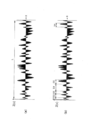
- FIG. 11 is a schematic diagram showing an example of a profile of a cut surface.
- the average line is a line drawn so as to make the upper and lower areas surrounded by this line equal, and the least square method (LS method) is usually applied.
- the X axis corresponds to an average line.
- FIG. 11B shows how to obtain the mountain interval Si straddling the average line when obtaining the average mountain interval Sm.
- the outer peripheral shape of the flange portion of the group lens is rectangular and the surface roughness of the four cut surfaces is cut so as to satisfy the conditional expressions (1) and (2).
- the shape of the outer periphery of the flange portion is a rectangle, each of which is a single material and is disposed between the flange portion and at least two lenses in which a lens portion is formed inside the flange portion, and the lens.
- Ra is an arithmetic average value of the profile displacement amount in the normal direction of the measurement plane from the average line
- L Evaluation length Z (x): When a profile is used, it is calculated by the following equation.
- Sm is the average distance between the peaks across the average line within the evaluation length
- Si Interval between the peaks straddling the average line
- n The number of peaks is calculated by the following formula.
- An imaging apparatus comprising: the combined lens according to any one of 4) to 6) above; and an imaging element that photoelectrically converts a subject image formed by the combined lens.
- ADVANTAGE OF THE INVENTION it becomes possible to provide the manufacturing method of a group lens which can suppress the fall of the contrast by stray light, and generation
- this group lens By using this group lens, the fall of contrast by stray light and generation
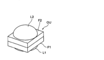
- FIG. 7 is a perspective view of a combined lens OU obtained through the steps shown in FIGS. 1 to 6.
- FIG. 7 is a flowchart summarizing the manufacturing process of the assembled lens described in FIGS. 1 to 6.
- FIG. It is a perspective view of the imaging device 50 using the group lens concerning this Embodiment.
- FIG. 10 is a cross-sectional view of the imaging device 50 shown in FIG. 9 taken along the line XIX-XIX and viewed in the direction of the arrow. It is the schematic diagram which showed an example of the profile of a cut surface. It is a schematic diagram which shows the typical example of the light beam path
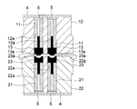
- 1 to 3 are schematic views showing a molding process of the lens array.
- a core support member 21 having a plurality of cores 23 (four cores in this example is described, but the figure is a cross-sectional view has two cores) attached to the upper end is shown as four.
- the lower mold 22 assembled in each of the two openings 22a is positioned below the platinum nozzle NZ communicating with a storage unit (not shown) in which the glass is heated and melted, and the droplets of the glass GL melted from the platinum nozzle NZ Is dripped.
- the viscosity of the glass GL is low, the dropped glass GL spreads on the upper surface of the lower mold 22 and easily enters the transfer surface 23a of the core 23 to transfer its shape.
- the amount of droplets of a relatively large glass GL that passes through the four small holes is adjusted, and then decomposed into four small droplets. At the same time, it may be supplied to the upper surface of the lower mold 22.
- the upper mold 12 in which the core support member 11 having a plurality of cores 13 (described in the present example with four members) attached to the lower ends is assembled in the four openings 12a.
- the lower mold 22 is brought close to the lower facing position and aligned with the upper mold 12.
- the upper mold 12 and the lower mold 22 are brought close to each other for molding. Thereby, the shape of the transfer surface 13a (here, convex shape) of the core 13 is transferred.
- a shallow circular step portion is formed around the transfer surface 13a for transferring a diaphragm housing portion for housing a diaphragm member SH described later, this is also transferred at the same time.
- the glass is cooled by holding the lower surface of the upper mold 12 and the upper surface of the lower mold 22 so as to be separated by a predetermined distance. The glass solidifies in a state where it goes around and covers the tapered portion 22g.
- the upper mold 12 and the lower mold 22 are separated from each other, and the glass is taken out to form a single material having four lens portions IM1b and IM1e having the same lens surface shape.
- the first lens array IM1 is molded.
- 1 to 3 show only the main part of the mold, and the holders for holding the upper mold 12 and the lower mold 22 are omitted.
- 4 is a bottom plate and 5 is a spacer.
- a second lens array IM2 having a lens surface shape different from that of the first lens array IM1 is formed using an upper die and a lower die having cores having different transfer surface shapes.
- the material forming the second lens array IM2 may be the same as or different from the material forming the first lens array IM1.
- 4 to 6 are schematic views showing a process for manufacturing a combined lens using a plurality of lens arrays after molding the lens array.
- the surface IM1a of the first lens array IM1 held by the jig JZ and the surface IM2a of the second lens array IM2 held by another jig JZ are opposed to each other.
- an adhesive is applied to at least one of the surface IM1a of the first lens array IM1 and the surface IM2a of the second lens array IM2.
- the diaphragm member SH may be an aperture diaphragm or a flare-cut diaphragm.
- the jig JZ is relatively approached and directly brought into contact with a contact portion formed at a portion other than the lens portions of the surfaces IM1a and IM2a, and the adhesive is solidified.
- the adhesive is solidified, a combined lens array IM3 in which the first lens array IM1 and the second lens array IM2 are bonded together is formed.
- the aperture member SH is interposed between recesses formed around the opposing lens portions so as not to hinder the contact between the first lens array IM1 and the second lens array IM2.
- the first lens array IM1 and the second lens array IM2 are in contact with each other so that the optical axes of the lens portion of the first lens array IM1 and the lens portion of the second lens array IM2 are substantially coincident with each other.
- the group lens array IM3 is cut by a dicing blade DB of a dicing machine that performs dicing at the position of the broken line shown in FIG. Get a lens.
- cutting may be performed using a slicing machine that performs slicing processing, or may be performed using a processing apparatus that can perform both dicing processing and slicing processing.
- This cutting position includes at least a portion of the surface IM1a of the first lens array IM1 and the surface IM2a of the second lens array IM2 that are bonded in contact with each other in order to maintain the accuracy of the interval between the opposing lens portions. So that it is cut.
- the combined lens according to the present embodiment is cut such that at least one cut surface has a surface roughness satisfying the following conditional expression at the time of cutting. 0.03 [ ⁇ m] ⁇ Ra ⁇ 0.30 [ ⁇ m] (1) 0 [ ⁇ m] ⁇ Sm ⁇ 30 [ ⁇ m] (2)
- Ra is an arithmetic average value of the profile displacement amount in the normal direction of the measurement plane from the average line, and is calculated by the following formula, where L is an evaluation length and Z (x) is a profile. It is.
- Sm is the average interval between the peaks across the average line within the evaluation length, where Si is the interval between the peaks across the average line and n is the number of peaks. It is.
- the grain size, rotational speed and feed speed of the dicing blade DB used are set so that at least one cut surface has a surface roughness satisfying the above conditional expressions (1) and (2). Is done.
- the grain size, rotation speed, and feed speed of the dicing blade DB with this surface roughness are determined in advance by experiments or the like.
- the amplitude of roughness can be reduced, and when stray light is incident, it can be uniformly scattered on the cut surface, thereby preventing the generation of high-intensity ghosts. .
- the outer peripheral side surface is a cylindrical surface
- the component in the regular reflection direction which is the strongest light component of the stray light reflected by the cylindrical surface even if the cylindrical surface is rough
- the component in the specular reflection direction is the center direction of the image sensor, only stray light from light incident from a specific direction, and most stray light is Since the light is reflected in a direction different from the center direction of the image sensor, it is possible to effectively prevent the ghost.
- the surface roughness is defined by the following conditional expressions (1 ′), (2 ′), 0.05 [ ⁇ m] ⁇ Ra ⁇ 0.20 [ ⁇ m] (1 ′) 5 [ ⁇ m] ⁇ Sm ⁇ 20 [ ⁇ m] (2 ′) It is more desirable to satisfy.
- conditional expression (1 ′) When the surface roughness of the cut surface exceeds the lower limit of the conditional expression (1 ′), stray light due to total reflection generated on the cut surface can be further reduced. By falling below the upper limit of the conditional expression (1 ′), it is possible to suppress a decrease in processing accuracy due to a more uneven roughness and to further reduce the occurrence of chipping at the cutting portion.
- conditional expression (2 ′) Furthermore, by exceeding the lower limit of the conditional expression (2 ′), it is possible to increase the feed speed of the dicing blade, and it is possible to reduce both the processing time and the ghost strength. In addition, by lowering the upper limit of the conditional expression (2 ′), the amplitude of roughness can be made smaller, and when stray light is incident, it can be scattered more uniformly on the cut surface, resulting in the generation of high-intensity ghosts. Can be prevented.
- the surface roughness can be measured using Talisurf manufactured by Ametech Co., Ltd. or UA3P manufactured by Panasonic Corporation, but is not limited to this, and other measuring devices may be used.
- FIG. 7 is a perspective view of the assembled lens OU obtained through the steps shown in FIGS.
- the group lens OU shown in FIG. 7 includes a first lens L1, a second lens L2, a rectangular plate-like flange portion F1 around the first lens L1, and a rectangular plate-like flange portion around the second lens L2.
- F2 and a diaphragm member SH disposed between the first lens L1 and the second lens L2.
- the outer peripheral side surface of the substantially rectangular flange portion F1 of the first lens L1 and the outer peripheral side surface of the substantially rectangular flange portion F2 of the second lens L2 formed by the above-described cutting step are rough surfaces of at least one surface thereof. Is formed so as to satisfy the above conditional expressions (1) and (2).
- the surface roughness of all the outer peripheral side surfaces is formed so as to satisfy the conditional expressions (1) and (2).
- the surface roughness of only one surface is formed so as to satisfy the conditional expressions (1) and (2)
- the surface roughness satisfying the conditional expressions (1) and (2) is satisfied. It is desirable to be incorporated in the imaging device so that the surface of the surface becomes the ground side when photographing is performed.
- FIG. 8 is a flowchart summarizing the manufacturing process of the assembled lens described in FIGS. This example will be described in the case of manufacturing a combined lens using two lens arrays.
- the first lens array IM1 formed of a single material is formed (step S101). This process is the process described with reference to FIGS.
- step S102 the second lens array IM2 formed of a single material is molded (step S102).
- step S102 a second surface having a lens surface shape different from that of the first lens array IM1 is obtained by using an upper die and a lower die having cores having different transfer surface shapes in the same process as in FIGS.
- the lens array IM2 is formed. Note that step S101 may be repeated when forming a combined lens by stacking two first lens arrays.
- a diaphragm member SH is disposed between the first lens array IM1 and the second lens array IM2, and an adhesive is applied to at least one of the surface IM1a of the first lens array IM1 and the surface IM2a of the second lens array IM2. Is applied (step S103). This step is the step described with reference to FIG.
- step S104 This step is the step described with reference to FIG.
- Step S106 This step is the step described with reference to FIG. Thereby, it is possible to obtain a group lens in which the outer peripheral side surface of the group lens OU has a surface roughness that satisfies the conditional expressions (1) and (2).
- FIG. 9 is a perspective view of an image pickup apparatus 50 using the combined lens according to the present embodiment.
- FIG. 10 is a view of the image pickup apparatus 50 shown in FIG. 9 cut along the arrow XIX-XIX line and viewed in the arrow direction. It is sectional drawing.
- the imaging device 50 includes a CMOS image sensor 51 as a solid-state imaging device having a photoelectric conversion unit 51a, and a combined lens OU that causes the photoelectric conversion unit 51a of the image sensor 51 to capture a subject image. And a substrate 52 having external connection terminals (not shown) for holding the image sensor 51 and transmitting and receiving electrical signals thereof, and these are integrally formed.
- a photoelectric conversion unit 51a in which pixels (photoelectric conversion elements) are two-dimensionally arranged is formed at a substantially central portion of the light receiving side plane, and is connected to a signal processing circuit (not shown).
- a signal processing circuit includes a drive circuit unit that sequentially drives each pixel to obtain a signal charge, an A / D conversion unit that converts each signal charge into a digital signal, and a signal that forms an image signal output using the digital signal. It consists of a processing unit and the like.
- a number of pads (not shown) are arranged near the outer edge of the plane on the light receiving side of the image sensor 51, and are connected to the substrate 52 via wires (not shown).
- the image sensor 51 converts the signal charge from the photoelectric conversion unit 51a into an image signal such as a digital YUV signal, and outputs the image signal to a predetermined circuit on the substrate 52 via a wire (not shown).
- Y is a luminance signal
- the solid-state imaging device is not limited to the above-described CMOS type image sensor, and other devices such as a CCD may be used.
- the substrate 52 that supports the image sensor 51 is communicably connected to the image sensor 51 through a wiring (not shown).
- the substrate 52 is connected to an external circuit (for example, a control circuit included in a host device of a portable terminal mounted with an imaging device) via an external connection terminal (not shown), and a voltage for driving the image sensor 51 from the external circuit. And a clock signal are supplied, and a digital YUV signal is output to an external circuit.
- an external circuit for example, a control circuit included in a host device of a portable terminal mounted with an imaging device
- an external connection terminal not shown
- a clock signal are supplied, and a digital YUV signal is output to an external circuit.
- An IR cut filter CG is disposed between the image sensor 51 and the second lens L2.
- the hollow rectangular tube-shaped lens frame 40 is open at the bottom, but the top is covered with a flange portion 40a.
- An opening 40b is formed in the center of the flange portion 40a.
- An assembled lens OU is disposed in the lens frame 40.
- the group lens OU includes, in order from the object side (upper side in FIG. 10), an aperture stop in which the opening edge of the lens frame functions, a first lens L1, a flare-cut stop member SH that blocks unnecessary light, and a second lens L2.
- the first lens L1 and the second lens L2 are made of glass, they have excellent optical characteristics.
- the tapered inner peripheral surface 40c of the opening 40b is brought into contact with the lens portion of the first lens L1 or a curved surface (not including the flange surface) obtained by extending the lens portion. The location is restricted by things. Thereby, the light receiving surface of the image sensor 51 can be accurately positioned at the focal position of the combined lens OU simply by placing the lens frame 40 on the substrate 52.
- the outer peripheral side surface of the assembled lens OU is bonded and fixed to the inner side surface of the lens frame 40 with an adhesive B as shown in the figure.
- this adhesive B it is preferable to use an opaque adhesive, particularly a black adhesive, and it is possible to further suppress a decrease in contrast and ghosting due to stray light.
- the present invention is not limited to this, and the present invention can be applied to the case where a combination lens is formed using three or more lens arrays. Needless to say.
- disconnected the group lens array by the dicing process was demonstrated, it is not restricted to this, You may cut
Landscapes
- Physics & Mathematics (AREA)
- Engineering & Computer Science (AREA)
- Optics & Photonics (AREA)
- General Physics & Mathematics (AREA)
- Chemical & Material Sciences (AREA)
- Manufacturing & Machinery (AREA)
- Organic Chemistry (AREA)
- Mechanical Engineering (AREA)
- Ophthalmology & Optometry (AREA)
- Health & Medical Sciences (AREA)
- Materials Engineering (AREA)
- Lens Barrels (AREA)
- Lenses (AREA)
Abstract
迷光によるコントラストの低下やゴーストの発生を抑制した組レンズの製造方法及び、組レンズを提供すること並びに、迷光によるコントラストの低下やゴーストの発生を抑制した撮像装置を得るために、それぞれが単一の材料で形成された少なくとも2つのレンズアレイを形成する工程と、形成されたレンズアレイの間に絞り部材を配置する工程と、レンズアレイ同士を当接させて積層し固着する工程と、固着されたレンズアレイを個々の組レンズに分離するための切断工程と、を有し、切断工程で、少なくとも1つの切断面が、以下の条件式、 0.03[μm]≦Ra≦0.30[μm] (1) 0[μm]<Sm≦30[μm] (2) を満足する面粗さとなるように切断する組レンズの製造方法とする。
Description
本発明は、2枚以上のレンズで構成された組レンズ、組レンズの製造方法及び、該組レンズを用いた撮像装置に関するものである。
コンパクトで非常に薄型の撮像装置(以下、カメラモジュールとも称す)が、携帯電話機やPDA(Personal Digital Assistant)等の携帯端末に用いられている。これらの携帯端末に使用される撮像素子としては、CCD型イメージセンサやCMOS型イメージセンサ等の固体撮像素子が知られている。近年では撮像素子の高画素化が進んでおり、高解像、高性能化が図られてきている。また、これら撮像素子上に被写体像を形成するための撮像レンズは、撮像素子の小型化に対応しコンパクト化が求められており、その要求は年々強まる傾向にある。
このような携帯端末に内蔵される撮像装置に用いる撮像レンズとして、樹脂レンズで構成される光学系が知られている。ここで、数インチのウェハ上にレプリカ法によって樹脂レンズ要素を同時に大量に成形し、それらをセンサウェハと組み合わせた後、切り離し、カメラモジュールを大量生産する手法が提案されている(例えば、特許文献1参照)。
しかしながら、樹脂は温度変化に対する屈折率変化が大きいため、撮像条件に関わらず高画質な画像を形成するためには、安定して光学機能を発揮できるガラスレンズを用いるのが好ましい。一方、従来のガラスレンズの製法では、複数のレンズを個々にガラスで成形した後、組み合わせていたため、手間がかかり大量生産に不向きであるという問題がある。
これに対し、ガラスを用いてレンズ部が複数成形されたレンズアレイを成形し、レンズアレイを積層して接着した後、切断して個々の組レンズを形成することが考えられている。
このような組レンズの場合、レンズ部の間隔精度を高めるためにレンズアレイ同士を当接させ固着して切断するよう構成した場合、レンズ部間に配置される絞り部材は、レンズ部に対応する一部にしか配置できない。このため、絞りで遮蔽されていないガラスの当接部を通過してくる迷光を遮断することができず、この迷光により結像した画像のコントラストの低下や、切断面での反射光がゴーストとなって写り込み、画質を低下させる問題がある。
図12は、絞りで遮蔽されていないガラスの当接部が有る場合の、ゴーストが発生する光線経路の代表的な例を示す模式図である。
図12に示すように、撮影範囲外からの高輝度の入射光は、図示矢印線で示すように絞り部材SHの無い、第1レンズL1、第2レンズL2の当接部を通過し外周面で反射してイメージセンサ51の光電変換部51aに達し、ゴーストとなって画質を低下させる。
本発明は上記問題に鑑み、迷光によるコントラストの低下やゴーストの発生を抑制できる組レンズの製造方法及び組レンズを提供すること並びに、該組レンズを用いることで迷光によるコントラストの低下やゴーストの発生を抑制した撮像装置を得ることを目的とするものである。
上記の目的は、下記の構成により達成される。
1)それぞれが単一の材料で形成された少なくとも2つのレンズアレイを形成する工程と、形成された前記レンズアレイの間に絞り部材を配置する工程と、前記レンズアレイ同士を当接させて積層し固着する工程と、固着されたレンズアレイを個々の組レンズに分離するための切断工程と、を有し、前記切断工程で、少なくとも1つの切断面が、以下の条件式を満足する面粗さとなるように切断することを特徴とする組レンズの製造方法。
0.03[μm]≦Ra≦0.30[μm] (1)
0[μm]<Sm≦30[μm] (2)
ただし、
Raは平均線からの測定平面の法線方向のプロファイル変位量の算術的平均値であって、
L:評価長さ
Z(x):プロファイル
としたとき、以下の式で算出される。
0.03[μm]≦Ra≦0.30[μm] (1)
0[μm]<Sm≦30[μm] (2)
ただし、
Raは平均線からの測定平面の法線方向のプロファイル変位量の算術的平均値であって、
L:評価長さ
Z(x):プロファイル
としたとき、以下の式で算出される。

Smは評価長さ内での平均線をまたぐ山の平均間隔であって、
Si:平均線をまたぐ山の間隔
n:山の数
としたとき、以下の式で算出される。
Si:平均線をまたぐ山の間隔
n:山の数
としたとき、以下の式で算出される。
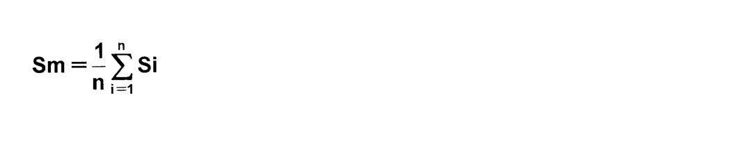
図11は、切断面のプロファイルの一例を示した模式図である。平均線とは、この線で囲まれてできる上下の面積を等しくするように引いた線であり、通常は最小自乗法(LS法)が適用される。なお、図11(a)、(b)ではX軸が平均線に相当する。また、図11(b)は、山の平均間隔Smを求める際の、平均線をまたぐ山の間隔Siの求め方を示している。
2)前記切断工程で、前記組レンズのフランジ部の外周形状が矩形でかつ4つの切断面の面粗さが、条件式(1)及び(2)を満足するように切断することを特徴とする前記1)に記載の組レンズの製造方法。
3)前記切断工程は、ダイシング加工もしくはスライシング加工で行われることを特徴とする前記1)又は前記2)に記載の組レンズの製造方法。
4)フランジ部の外周の形状が矩形であって、それぞれが単一の材料で前記フランジ部及び前記フランジ部の内側にレンズ部が形成された少なくとも2枚のレンズと、前記レンズの間に配置された少なくとも一つの絞り部材と、を有し、前記レンズを、それぞれ前記フランジ部に形成された当接部で当接させて固着した組レンズであって、前記組レンズの外周側面のうち、少なくとも一つの面の面粗さが、以下の条件式を満足することを特徴とする組レンズ。
0.03[μm]≦Ra≦0.30[μm] (1)
0[μm]<Sm≦30[μm] (2)
ただし、
Raは平均線からの測定平面の法線方向のプロファイル変位量の算術的平均値であって、
L:評価長さ
Z(x):プロファイル
としたとき、以下の式で算出される。
0.03[μm]≦Ra≦0.30[μm] (1)
0[μm]<Sm≦30[μm] (2)
ただし、
Raは平均線からの測定平面の法線方向のプロファイル変位量の算術的平均値であって、
L:評価長さ
Z(x):プロファイル
としたとき、以下の式で算出される。
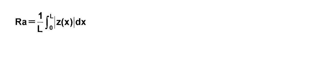
Smは評価長さ内での平均線をまたぐ山の平均間隔であって、
Si:平均線をまたぐ山の間隔
n:山の数
としたとき、以下の式で算出される。
Si:平均線をまたぐ山の間隔
n:山の数
としたとき、以下の式で算出される。

5)前記組レンズの外周側面の全てが、条件式(1)及び(2)を満足することを特徴とする前記4)に記載の組レンズ。
6)前記組レンズは、前記外周側面で不透明な接着剤により鏡枠に接着されていることを特徴とする前記4)又は前記5)に記載の組レンズ。
7)前記4)から前記6)までのいずれかに記載の組レンズと、前記組レンズで形成された被写体像を光電変換する撮像素子と、を有することを特徴とする撮像装置。
本発明によれば、迷光によるコントラストの低下やゴーストの発生を抑制できる組レンズの製造方法及び組レンズを提供することが可能となり、該組レンズを用いることで迷光によるコントラストの低下やゴーストの発生を抑制した撮像装置を得ることが可能となる。
以下、実施の形態により本発明を詳しく説明するが、本発明はこれに限定されるものではない。
図1~図3は、レンズアレイの成形工程を示す模式図である。
図1に示すように、複数のコア23(本例ではコアが4つのもので説明するが、図は断面図のためコアが2つとなっている)を上端に取り付けたコア支持部材21を4つの開孔22a内にそれぞれ組み付けた下金型22を、ガラスを加熱溶融させた貯蔵部(不図示)に連通する白金ノズルNZの下方に位置させ、白金ノズルNZから溶融したガラスGLの液滴を滴下させる。かかる状態では、ガラスGLの粘度は低いので、落下したガラスGLは、下金型22の上面に広がり、コア23の転写面23a内に容易に進入してその形状が転写される。また、小さな液滴の個別摘下を行う場合には比較的大きなガラスGLの液滴を4つの小孔を通過させて滴下する量を調整した上、4つの小さな液滴に分解して、略同時に下金型22の上面に供給すればよい。
次いで、ガラスGLが冷却する前に、複数のコア13(本例では4つのもので説明する)を下端に取り付けたコア支持部材11を4つの開孔12a内にそれぞれ組み付けた上金型12の下方の対向する位置まで、下金型22を接近させ、上金型12に整合させる。
更に、図2に示すように、上金型12と下金型22とを接近させて成形を行う。これにより、コア13の転写面13a(ここでは凸形状)の形状を転写する。尚、転写面13aの周囲には、後述する絞り部材SHを収容する絞り収容部を転写するための浅い円形段部が形成されているので、これも同時に転写する。このとき、上金型12の下面と下金型22の上面とが、所定の距離で離間するように保持してガラスを冷却させる。ガラスは、周囲に回り込んでテーパ部22gを覆った状態で固化する。
その後、図3に示すように上金型12と下金型22とを離間させ、ガラスを取り出すことで、4つの同一レンズ面形状のレンズ部IM1b、IM1eを有する単一の材料で形成された第1のレンズアレイIM1が成形される。
なお、図1~3では、金型の主要部のみを示しており、上金型12と下金型22とをそれぞれ保持するホルダ等は省略してある。また、4は底板、5はスペーサである。
同様の工程で、異なる転写面形状のコアを備えた上金型と下金型を用いて、第1のレンズアレイIM1と異なるレンズ面形状を有する第2のレンズアレイIM2が成形される。第2のレンズアレイIM2を形成する材料は、第1のレンズアレイIM1を形成する材料と同じであっても、異なる材料であってもよい。
図4~図6は、レンズアレイ成形後の複数枚のレンズアレイを用いて組レンズを製造する工程を示す模式図である。
図4に示すように、治具JZにより保持された第1のレンズアレイIM1の表面IM1aと、別の治具JZにより保持された第2のレンズアレイIM2の表面IM2aとを対向させ、4つのドーナツ板状の絞り部材SHをレンズ部IM1bの周囲に形成した絞り収容部に配置した上で、第1のレンズアレイIM1の表面IM1aと第2のレンズアレイIM2の表面IM2aの少なくとも一方に接着材を塗布する。
なお、絞り部材SHは、開口絞りであってもフレアカット用の絞りであってもよい。
次いで、図5に示すように、治具JZを相対的に接近させ表面IM1a、IM2aのレンズ部以外の部位に形成された当接部で直接的に当接させて、接着剤の固化を待つ。接着剤が固化することで、第1のレンズアレイIM1と第2のレンズアレイIM2とを貼り合わせた組レンズアレイIM3が形成される。
なお、絞り部材SHは、第1のレンズアレイIM1と第2のレンズアレイIM2の当接を阻害しないように、相対するレンズ部周辺に形成された凹部に間挿されている。また、第1のレンズアレイIM1のレンズ部と第2のレンズアレイIM2のレンズ部は、それぞれの光軸が略一致するように第1のレンズアレイIM1と第2のレンズアレイIM2が当接しているのはもちろんである。
その後、治具JZを離間させ、組レンズアレイIM3を取り出す。
組レンズアレイIM3を取り出した後、図6に示す破線の位置で、ダイシング加工を行うダイシングマシンのダイシングブレードDBにより、組レンズアレイIM3を切断して、フランジ部の外周形状が矩形の個々の組レンズを得る。なお、この切断時には、スライシング加工を行うスライシングマシンを用いて切断してもよいし、ダイシング加工とスライシング加工のどちらも行うことのできる加工装置を用いて切断してもよい。なお、この切断する位置は、相対するレンズ部の間隔精度を維持するため、少なくとも当接して接着された第1のレンズアレイIM1の表面IM1aと第2のレンズアレイIM2の表面IM2aの部位を含むように切断される。
本実施の形態に係る組レンズは、この切断時に、少なくとも1つの切断面が以下の条件式を満足する面粗さとなるように切断される。
0.03[μm]≦Ra≦0.30[μm] (1)
0[μm]<Sm≦30[μm] (2)
ただし、
Raは平均線からの測定平面の法線方向のプロファイル変位量の算術的平均値であって、Lを評価長さ、Z(x)をプロファイル、としたとき、以下の式で算出されるものである。
0.03[μm]≦Ra≦0.30[μm] (1)
0[μm]<Sm≦30[μm] (2)
ただし、
Raは平均線からの測定平面の法線方向のプロファイル変位量の算術的平均値であって、Lを評価長さ、Z(x)をプロファイル、としたとき、以下の式で算出されるものである。

また、Smは評価長さ内での平均線をまたぐ山の平均間隔であって、Siを平均線をまたぐ山の間隔、nを山の数、としたとき、以下の式で算出されるものである。

すなわち、少なくとも1つの切断面は上記条件式(1)、(2)を満足する面粗さとなるように、使用するダイシングブレードDBの砥粒の粒径、回転速度及び送り速度が設定されて切断される。この面粗さとするダイシングブレードDBの砥粒の粒径、回転速度及び送り速度は、予め実験等で決められたものである。なお、組レンズとなる4つの外周面全てが、上記条件式(1)及び(2)を満足する面粗さとなるように切断するのが、より好ましい。
切断面の面粗さが、上記条件式(1)の下限を上回ることで、切断面で発生する全反射による迷光を低減させることができる。また上記条件式(1)の上限を下回ることで、切断面の起伏が過度になることを防止し、粗さの不均一による加工精度の低下を抑え、切断部でのチッピングの発生を低減させることができる。
更に、上記条件式(2)の上限を下回ることで、粗さの振幅を小さくでき、迷光が入射した際に、切断面で均一に散乱させることができ、高強度のゴーストの発生を防止できる。
また、外周側面が円筒面となっている場合、円筒面を粗面としても円筒面で反射される迷光のうち最も強い光成分となる正反射方向の成分はイメージセンサの中心方向に反射されることになるが、切断された外周側面が平面で構成されている場合には正反射方向の成分がイメージセンサの中心方向となるのは特定の方向から入射した光による迷光のみでほとんどの迷光はイメージセンサの中心方向とは異なる方向に反射されることになるのでゴースト発生を効果的に防止できる。
これにより、迷光によるコントラストの低下やゴーストの発生を抑制した組レンズを得ることができる。
なお、面粗さは、以下の条件式(1′)、(2′)、
0.05[μm]≦Ra≦0.20[μm] (1′)
5[μm]<Sm≦20[μm] (2′)
を満たすと、より望ましい。
0.05[μm]≦Ra≦0.20[μm] (1′)
5[μm]<Sm≦20[μm] (2′)
を満たすと、より望ましい。
切断面の面粗さが、上記条件式(1′)の下限を上回ることで、切断面で発生する全反射による迷光をより低減させることができるようになる。上記条件式(1′)の上限を下回ることで、より粗さの不均一による加工精度の低下を抑え、切断部でのチッピングの発生をより低減させることができるようになる。
更に、上記条件式(2′)の下限を上回ることで、ダイシングブレードの送り速度を速くすることができ、加工工程の時間短縮とゴースト強度の低減の両立が可能となる。また、上記条件式(2′)の上限を下回ることで、粗さの振幅をより小さくでき、迷光が入射した際に、切断面でより均一に散乱させることができ、高強度のゴーストの発生を防止できるようになる。
なお、面粗さの測定は、アメテック株式会社製のタリサーフや、パナソニック株式会社製のUA3Pを使用することができるが、これに限るものでなく、その他の測定器を用いてもよい。
図7は、図1~図6に示す工程を経て得られた組レンズOUの斜視図である。
図7に示す組レンズOUは、第1レンズL1と、第2レンズL2と、第1レンズL1の周囲の矩形板状のフランジ部F1と、第2レンズL2の周囲の矩形板状のフランジ部F2と、第1レンズL1と第2レンズL2の間に配置された絞り部材SHとを有する。上述の切断工程により形成された、第1レンズL1の略矩形状のフランジ部F1の外周側面及び第2レンズL2の略矩形状のフランジ部F2の外周側面は、その少なくとも一つの面の面粗さが上記条件式(1)、(2)を満足するように形成されている。
なお、外周側面の全ての面の面粗さが上記条件式(1)、(2)を満足するように形成されていると、より好ましい。
また、一つの面の面粗さのみが上記条件式(1)、(2)を満足するように形成されている場合には、上記条件式(1)、(2)を満足する面粗さの面が撮影の行われる際に地面側となるよう撮像装置に組み込まれることが望ましい。
図8は、図1~図6で説明した組レンズの製造工程をまとめたフローチャートである。なお、本例は、2枚のレンズアレイを用いて組レンズを製造する場合で説明する。
図8のフローに示すように、本実施の形態に係る組レンズの製造は、まず、単一の材料で形成される第1のレンズアレイIM1を成形する(ステップS101)。この工程が、上述の図1~図3で説明した工程である。
次いで、単一の材料で形成される第2のレンズアレイIM2を成形する(ステップS102)。ステップS102では、図1~図3と同様の工程で、異なる転写面形状のコアを備えた上金型と下金型を用いて、第1のレンズアレイIM1と異なるレンズ面形状を有する第2のレンズアレイIM2を成形する。なお、第1のレンズアレイを2枚積層して組レンズを形成する場合には、ステップS101を繰り返せばよい。
次いで、第1のレンズアレイIM1と第2のレンズアレイIM2の間に絞り部材SHを配置し、第1のレンズアレイIM1の表面IM1aと第2のレンズアレイIM2の表面IM2aの少なくとも一方に接着材を塗布する(ステップS103)。この工程が、上述の図4で説明した工程である。
次いで、第1のレンズアレイIM1と第2のレンズアレイIM2をレンズ部以外の部位に形成された当接部で直接的に当接、積層し、接着剤を固化させる(ステップS104)。この工程が、上述の図5で説明した工程である。
この後、治具JZを離間させ、組レンズアレイIM3を取り出す(ステップS105)。
次いで、組レンズアレイIM3を、その切断面が上記条件式(1)、(2)を満足する面粗さとなるような、ダイシングブレードDBの回転速度及び送り速度で個別の組レンズOUに切断する(ステップS106)。この工程が、上述の図6で説明した工程である。これにより、組レンズOUの外周側面が、上記条件式(1)、(2)を満足する面粗さとなった組レンズを得ることができる。
切断工程で、上記条件式(1)、(2)を満足する面粗さとなるよう切断することで、ブラスト等の別工程を設けることなく安価な、迷光によるコントラストの低下やゴーストの発生を抑制する適切な粗し面を形成することができる。
図9は、本実施の形態にかかる組レンズを使用した撮像装置50の斜視図であり、図10は、図9に示す撮像装置50を矢印XIX-XIX線で切断して矢印方向に見た断面図である。
図10に示すように、撮像装置50は、光電変換部51aを有する固体撮像素子としてのCMOS型のイメージセンサ51と、このイメージセンサ51の光電変換部51aに被写体像を撮像させる組レンズOUと、イメージセンサ51を保持すると共にその電気信号の送受を行う外部接続用端子(不図示)を有する基板52とを備え、これらが一体的に形成されている。
イメージセンサ51は、その受光側の平面の略中央部に、画素(光電変換素子)が2次元的に配置された、光電変換部51aが形成されており、不図示の信号処理回路に接続されている。かかる信号処理回路は、各画素を順次駆動し信号電荷を得る駆動回路部と、各信号電荷をデジタル信号に変換するA/D変換部と、このデジタル信号を用いて画像信号出力を形成する信号処理部等から構成されている。また、イメージセンサ51の受光側の平面の外縁近傍には、多数のパッド(図示略)が配置されており、不図示のワイヤを介して基板52に接続されている。イメージセンサ51は、光電変換部51aからの信号電荷をデジタルYUV信号等の画像信号等に変換し、ワイヤ(不図示)を介して基板52上の所定の回路に出力する。ここで、Yは輝度信号、U(=R-Y)は赤と輝度信号との色差信号、V(=B-Y)は青と輝度信号との色差信号である。なお、固体撮像素子は上記CMOS型のイメージセンサに限定されるものではなく、CCD等の他のものを使用してもよい。
イメージセンサ51を支持する基板52は、不図示の配線により、イメージセンサ51に対して通信可能に接続されている。
基板52は、不図示の外部接続用端子を介して外部回路(例えば、撮像装置を実装した携帯端末の上位装置が有する制御回路)と接続され、外部回路からイメージセンサ51を駆動するための電圧やクロック信号の供給を受け、また、デジタルYUV信号を外部回路へ出力する。
イメージセンサ51と第2レンズL2との間にIRカットフィルタCGが配置されている。中空角筒状の鏡枠40は下部が開放しているが、上部はフランジ部40aで覆われている。フランジ部40aの中央には開口40bが形成されている。鏡枠40内に組レンズOUが配置されている。
組レンズOUは、物体側(図10で上方)より順に、鏡枠の開口縁が機能する開口絞り、第1レンズL1、不要光を遮光するフレアカット用の絞り部材SH、第2レンズL2を有する。上述したように第1レンズL1、第2レンズL2はガラス製であるので光学特性に優れる。本実施の形態では、第1レンズL1のレンズ部、又はレンズ部を延長した曲面(但しフランジ面を含まない)に対して、開口40bのテーパ状の内周面40cを当該レンズに当接させる事で位置規制している。これにより鏡枠40を基板52上に載置するだけで、組レンズOUの焦点位置にイメージセンサ51の受光面を精度良く位置決めすることができる。
組レンズOUの外周側面は、図示の如く、鏡枠40の内側面に接着剤Bで接着固定されている。この接着剤Bは、不透明の接着剤、特に黒色の接着剤を用いることが好ましく、迷光によるコントラストの低下やゴーストの発生をより抑制することができる。
なお、上述の説明では、レンズアレイを2つ用いた組レンズで説明したが、これに限るものでなく、3つ以上のレンズアレイを用いて組レンズを形成する場合にも適用可能であるのは言うまでもない。また、4つのコアが組み込まれた金型を例にして説明したが、これに限るものでないのはいうまでもない。また、ダイシング加工により組レンズアレイを切断した例で説明したが、これに限らず、スライシング加工により切断しても良い。
12 上金型
13 コア
13a 転写面
22 下金型
22g テーパ部
23 コア
23a 転写面
40 鏡枠
40b 開口
50 撮像装置
51 イメージセンサ
51a 光電変換部
52 基板
B 接着剤
CG IRカットフィルタ
DB ダイシングブレード
IM1 第1のレンズアレイ
IM2 第2のレンズアレイ
IM3 組レンズアレイ
JZ 治具
L1 第1レンズ
L2 第2レンズ
NZ 白金ノズル
OU 組レンズ
SH 絞り部材
13 コア
13a 転写面
22 下金型
22g テーパ部
23 コア
23a 転写面
40 鏡枠
40b 開口
50 撮像装置
51 イメージセンサ
51a 光電変換部
52 基板
B 接着剤
CG IRカットフィルタ
DB ダイシングブレード
IM1 第1のレンズアレイ
IM2 第2のレンズアレイ
IM3 組レンズアレイ
JZ 治具
L1 第1レンズ
L2 第2レンズ
NZ 白金ノズル
OU 組レンズ
SH 絞り部材
Claims (7)
- それぞれが単一の材料で形成された少なくとも2つのレンズアレイを形成する工程と、
形成された前記レンズアレイの間に絞り部材を配置する工程と、
前記レンズアレイ同士を当接させて積層し固着する工程と、
固着されたレンズアレイを個々の組レンズに分離するための切断工程と、を有し、
前記切断工程で、少なくとも1つの切断面が、以下の条件式を満足する面粗さとなるように切断することを特徴とする組レンズの製造方法。
0.03[μm]≦Ra≦0.30[μm] (1)
0[μm]<Sm≦30[μm] (2)
ただし、
Raは平均線からの測定平面の法線方向のプロファイル変位量の算術的平均値であって、
L:評価長さ
Z(x):プロファイル
としたとき、以下の式で算出される。

Smは評価長さ内での平均線をまたぐ山の平均間隔であって、
Si:平均線をまたぐ山の間隔
n:山の数
としたとき、以下の式で算出される。

- 前記切断工程で、前記組レンズのフランジ部の外周形状が矩形でかつ4つの切断面の面粗さが、条件式(1)及び(2)を満足するように切断することを特徴とする請求項1に記載の組レンズの製造方法。
- 前記切断工程は、ダイシング加工もしくはスライシング加工で行われることを特徴とする請求項1又は請求項2に記載の組レンズの製造方法。
- フランジ部の外周の形状が矩形であって、それぞれが単一の材料で前記フランジ部及び前記フランジ部の内側にレンズ部が形成された少なくとも2枚のレンズと、
前記レンズの間に配置された少なくとも一つの絞り部材と、を有し、
前記レンズを、それぞれ前記フランジ部に形成された当接部で当接させて固着した組レンズであって、
前記組レンズの外周側面のうち、少なくとも一つの面の面粗さが、以下の条件式を満足することを特徴とする組レンズ。
0.03[μm]≦Ra≦0.30[μm] (1)
0[μm]<Sm≦30[μm] (2)
ただし、
Raは平均線からの測定平面の法線方向のプロファイル変位量の算術的平均値であって、
L:評価長さ
Z(x):プロファイル
としたとき、以下の式で算出される。

Smは評価長さ内での平均線をまたぐ山の平均間隔であって、
Si:平均線をまたぐ山の間隔
n:山の数
としたとき、以下の式で算出される。

- 前記組レンズの外周側面の全てが、条件式(1)及び(2)を満足することを特徴とする請求項4に記載の組レンズ。
- 前記組レンズは、前記外周側面で不透明な接着剤により鏡枠に接着されていることを特徴とする請求項4又は請求項5に記載の組レンズ。
- 請求項4から請求項6までのいずれか一項に記載の組レンズと、
前記組レンズで形成された被写体像を光電変換する撮像素子と、を有することを特徴とする撮像装置。
Priority Applications (1)
| Application Number | Priority Date | Filing Date | Title |
|---|---|---|---|
| JP2012501723A JPWO2011105201A1 (ja) | 2010-02-24 | 2011-02-07 | 組レンズの製造方法、組レンズ及び撮像装置 |
Applications Claiming Priority (2)
| Application Number | Priority Date | Filing Date | Title |
|---|---|---|---|
| JP2010-038454 | 2010-02-24 | ||
| JP2010038454 | 2010-02-24 |
Publications (1)
| Publication Number | Publication Date |
|---|---|
| WO2011105201A1 true WO2011105201A1 (ja) | 2011-09-01 |
Family
ID=44506617
Family Applications (1)
| Application Number | Title | Priority Date | Filing Date |
|---|---|---|---|
| PCT/JP2011/052485 Ceased WO2011105201A1 (ja) | 2010-02-24 | 2011-02-07 | 組レンズの製造方法、組レンズ及び撮像装置 |
Country Status (2)
| Country | Link |
|---|---|
| JP (1) | JPWO2011105201A1 (ja) |
| WO (1) | WO2011105201A1 (ja) |
Cited By (6)
| Publication number | Priority date | Publication date | Assignee | Title |
|---|---|---|---|---|
| WO2014042060A1 (ja) * | 2012-09-15 | 2014-03-20 | コニカミノルタ株式会社 | レンズアレイ、レンズアレイ積層体、レンズアレイの製造方法、レンズアレイ積層体の製造方法及びレンズユニットの製造方法 |
| JP2016085445A (ja) * | 2014-10-24 | 2016-05-19 | 日本電気硝子株式会社 | 光学レンズアレイ及び光学レンズ |
| JP5951092B1 (ja) * | 2015-08-31 | 2016-07-13 | パナソニック株式会社 | 内視鏡 |
| WO2017090520A1 (ja) * | 2015-11-24 | 2017-06-01 | コニカミノルタ株式会社 | 光学素子及び光学装置 |
| US9838576B2 (en) | 2015-08-31 | 2017-12-05 | Panasonic Corporation | Endoscope |
| CN110587670A (zh) * | 2019-10-14 | 2019-12-20 | 浙江舜宇光学有限公司 | 一种用于塑胶透镜浇口的剪切刀片 |
Citations (7)
| Publication number | Priority date | Publication date | Assignee | Title |
|---|---|---|---|---|
| JPH07333408A (ja) * | 1994-06-10 | 1995-12-22 | Olympus Optical Co Ltd | レンズおよびその製造方法 |
| JPH11326604A (ja) * | 1998-05-11 | 1999-11-26 | Enplas Corp | レンズ及び光学機器 |
| JP2001033677A (ja) * | 1999-07-26 | 2001-02-09 | Nikon Corp | 光学部品の保持構造 |
| JP2006039012A (ja) * | 2004-07-23 | 2006-02-09 | Hitachi Maxell Ltd | プラスチックレンズ及びプラスチックレンズの製造方法 |
| JP2007310276A (ja) * | 2006-05-22 | 2007-11-29 | Sharp Corp | レンズユニットおよびその製造方法、並びにカメラモジュール |
| WO2008096584A1 (ja) * | 2007-02-07 | 2008-08-14 | Konica Minolta Opto, Inc. | 撮像装置の製造方法及び撮像装置並びに携帯端末 |
| WO2010001955A1 (ja) * | 2008-07-04 | 2010-01-07 | コニカミノルタオプト株式会社 | 撮像レンズ、その製造方法及び撮像ユニット |
-
2011
- 2011-02-07 JP JP2012501723A patent/JPWO2011105201A1/ja active Pending
- 2011-02-07 WO PCT/JP2011/052485 patent/WO2011105201A1/ja not_active Ceased
Patent Citations (7)
| Publication number | Priority date | Publication date | Assignee | Title |
|---|---|---|---|---|
| JPH07333408A (ja) * | 1994-06-10 | 1995-12-22 | Olympus Optical Co Ltd | レンズおよびその製造方法 |
| JPH11326604A (ja) * | 1998-05-11 | 1999-11-26 | Enplas Corp | レンズ及び光学機器 |
| JP2001033677A (ja) * | 1999-07-26 | 2001-02-09 | Nikon Corp | 光学部品の保持構造 |
| JP2006039012A (ja) * | 2004-07-23 | 2006-02-09 | Hitachi Maxell Ltd | プラスチックレンズ及びプラスチックレンズの製造方法 |
| JP2007310276A (ja) * | 2006-05-22 | 2007-11-29 | Sharp Corp | レンズユニットおよびその製造方法、並びにカメラモジュール |
| WO2008096584A1 (ja) * | 2007-02-07 | 2008-08-14 | Konica Minolta Opto, Inc. | 撮像装置の製造方法及び撮像装置並びに携帯端末 |
| WO2010001955A1 (ja) * | 2008-07-04 | 2010-01-07 | コニカミノルタオプト株式会社 | 撮像レンズ、その製造方法及び撮像ユニット |
Cited By (11)
| Publication number | Priority date | Publication date | Assignee | Title |
|---|---|---|---|---|
| WO2014042060A1 (ja) * | 2012-09-15 | 2014-03-20 | コニカミノルタ株式会社 | レンズアレイ、レンズアレイ積層体、レンズアレイの製造方法、レンズアレイ積層体の製造方法及びレンズユニットの製造方法 |
| CN104620139A (zh) * | 2012-09-15 | 2015-05-13 | 柯尼卡美能达株式会社 | 透镜阵列、透镜阵列层叠体、透镜阵列的制造方法、透镜阵列层叠体的制造方法以及透镜单元的制造方法 |
| CN104620139B (zh) * | 2012-09-15 | 2017-05-24 | 柯尼卡美能达株式会社 | 透镜阵列、其层叠体及制造方法、透镜单元的制造方法 |
| US10481303B2 (en) | 2012-09-15 | 2019-11-19 | Konica Minolta, Inc. | Lens array, lens array laminate body , lens array manufacturing method, lens array laminate body manufacturing method, and lens unit manufacturing method |
| JP2016085445A (ja) * | 2014-10-24 | 2016-05-19 | 日本電気硝子株式会社 | 光学レンズアレイ及び光学レンズ |
| JP5951092B1 (ja) * | 2015-08-31 | 2016-07-13 | パナソニック株式会社 | 内視鏡 |
| US9838576B2 (en) | 2015-08-31 | 2017-12-05 | Panasonic Corporation | Endoscope |
| US10389921B2 (en) | 2015-08-31 | 2019-08-20 | Panasonic Corporation | Endoscope |
| US10560612B2 (en) | 2015-08-31 | 2020-02-11 | Panasonic I-Pro Sensing Solutions Co., Ltd. | Endoscope |
| WO2017090520A1 (ja) * | 2015-11-24 | 2017-06-01 | コニカミノルタ株式会社 | 光学素子及び光学装置 |
| CN110587670A (zh) * | 2019-10-14 | 2019-12-20 | 浙江舜宇光学有限公司 | 一种用于塑胶透镜浇口的剪切刀片 |
Also Published As
| Publication number | Publication date |
|---|---|
| JPWO2011105201A1 (ja) | 2013-06-20 |
Similar Documents
| Publication | Publication Date | Title |
|---|---|---|
| EP1389804B1 (en) | CMOS image sensor using gradient index chip scale lenses | |
| JP5267825B2 (ja) | 撮像レンズ、撮像装置、デジタル機器、及び撮像レンズの製造方法 | |
| TWI512956B (zh) | 光學成像裝置及其製造方法 | |
| US20100044815A1 (en) | Cmos image sensor package and camera module using same | |
| CN101632294B (zh) | 摄像装置及摄像装置的制造方法 | |
| US20070117249A1 (en) | Microelectronic imaging units and methods of manufacturing microelectronic imaging units | |
| EP2477071A1 (en) | Camera module and method of manufacturing the same | |
| WO2011105201A1 (ja) | 組レンズの製造方法、組レンズ及び撮像装置 | |
| US9304293B2 (en) | Imaging lens, imaging apparatus and mobile terminal device | |
| WO2006109638A1 (ja) | 固体撮像素子及びその製造方法 | |
| TWI768105B (zh) | 光學成像模組、成像系統及其製造方法 | |
| TW202009556A (zh) | 光學成像模組、成像系統及其製造方法 | |
| TW202009586A (zh) | 光學成像模組、成像系統及其製造方法 | |
| TW202013038A (zh) | 光學成像模組 | |
| TW202009540A (zh) | 光學成像模組、成像系統及其製造方法 | |
| US20120300320A1 (en) | Method for Manufacturing Lens Unit, Imaging Device, Method for Manufacturing Mold, Mold For Molding, and Method for Molding Glass Lens Array | |
| TW202009590A (zh) | 光學成像模組、成像系統及其製造方法 | |
| TWI768125B (zh) | 光學成像模組及其成像系統、製造方法 | |
| TWI746881B (zh) | 光學成像模組、成像系統及其製造方法 | |
| TWI768104B (zh) | 光學成像模組、光學成像系統及其製造方法 | |
| TW202009541A (zh) | 光學成像模組、成像系統及其製造方法 | |
| CN110941070A (zh) | 光学成像模块 | |
| TW202012991A (zh) | 光學成像模組 | |
| TW202009585A (zh) | 光學成像模組、成像系統及其製造方法 | |
| JPWO2015019768A1 (ja) | レンズアレイ、レンズアレイ積層体、及び、これらの製造方法 |
Legal Events
| Date | Code | Title | Description |
|---|---|---|---|
| 121 | Ep: the epo has been informed by wipo that ep was designated in this application |
Ref document number: 11747165 Country of ref document: EP Kind code of ref document: A1 |
|
| WWE | Wipo information: entry into national phase |
Ref document number: 2012501723 Country of ref document: JP |
|
| NENP | Non-entry into the national phase |
Ref country code: DE |
|
| 122 | Ep: pct application non-entry in european phase |
Ref document number: 11747165 Country of ref document: EP Kind code of ref document: A1 |