WO2011105047A1 - In-Ga-Sn OXIDE SINTER, TARGET, OXIDE SEMICONDUCTOR FILM, AND SEMICONDUCTOR ELEMENT - Google Patents
In-Ga-Sn OXIDE SINTER, TARGET, OXIDE SEMICONDUCTOR FILM, AND SEMICONDUCTOR ELEMENT Download PDFInfo
- Publication number
- WO2011105047A1 WO2011105047A1 PCT/JP2011/000972 JP2011000972W WO2011105047A1 WO 2011105047 A1 WO2011105047 A1 WO 2011105047A1 JP 2011000972 W JP2011000972 W JP 2011000972W WO 2011105047 A1 WO2011105047 A1 WO 2011105047A1
- Authority
- WO
- WIPO (PCT)
- Prior art keywords
- oxide
- sintered body
- oxide sintered
- less
- film
- Prior art date
Links
- 239000004065 semiconductor Substances 0.000 title claims description 66
- 229910052733 gallium Inorganic materials 0.000 claims abstract description 16
- 229910052738 indium Inorganic materials 0.000 claims abstract description 16
- 229910052718 tin Inorganic materials 0.000 claims abstract description 16
- APFVFJFRJDLVQX-UHFFFAOYSA-N indium atom Chemical compound [In] APFVFJFRJDLVQX-UHFFFAOYSA-N 0.000 claims abstract description 8
- ATJFFYVFTNAWJD-UHFFFAOYSA-N Tin Chemical compound [Sn] ATJFFYVFTNAWJD-UHFFFAOYSA-N 0.000 claims abstract description 7
- GYHNNYVSQQEPJS-UHFFFAOYSA-N Gallium Chemical compound [Ga] GYHNNYVSQQEPJS-UHFFFAOYSA-N 0.000 claims abstract description 6
- 238000005477 sputtering target Methods 0.000 claims description 27
- 239000000203 mixture Substances 0.000 claims description 24
- 238000004519 manufacturing process Methods 0.000 claims description 22
- 239000013078 crystal Substances 0.000 claims description 20
- 239000002994 raw material Substances 0.000 claims description 18
- 150000001875 compounds Chemical class 0.000 claims description 17
- 239000011701 zinc Substances 0.000 claims description 12
- 238000000227 grinding Methods 0.000 claims description 11
- 239000000843 powder Substances 0.000 claims description 11
- 238000002156 mixing Methods 0.000 claims description 7
- HCHKCACWOHOZIP-UHFFFAOYSA-N Zinc Chemical compound [Zn] HCHKCACWOHOZIP-UHFFFAOYSA-N 0.000 claims description 6
- 229910052725 zinc Inorganic materials 0.000 claims description 6
- 108091006149 Electron carriers Proteins 0.000 claims description 4
- 239000010408 film Substances 0.000 description 81
- 238000000034 method Methods 0.000 description 53
- 239000010409 thin film Substances 0.000 description 30
- 230000008569 process Effects 0.000 description 28
- 239000010410 layer Substances 0.000 description 26
- 238000005245 sintering Methods 0.000 description 23
- 238000004544 sputter deposition Methods 0.000 description 21
- XLOMVQKBTHCTTD-UHFFFAOYSA-N Zinc monoxide Chemical compound [Zn]=O XLOMVQKBTHCTTD-UHFFFAOYSA-N 0.000 description 20
- 238000005530 etching Methods 0.000 description 19
- 238000002441 X-ray diffraction Methods 0.000 description 16
- 229910052760 oxygen Inorganic materials 0.000 description 16
- 238000000465 moulding Methods 0.000 description 14
- 239000000758 substrate Substances 0.000 description 14
- 238000001039 wet etching Methods 0.000 description 14
- 230000015572 biosynthetic process Effects 0.000 description 13
- 239000000243 solution Substances 0.000 description 12
- 229910004298 SiO 2 Inorganic materials 0.000 description 11
- 238000001354 calcination Methods 0.000 description 11
- 229910003437 indium oxide Inorganic materials 0.000 description 11
- PJXISJQVUVHSOJ-UHFFFAOYSA-N indium(iii) oxide Chemical compound [O-2].[O-2].[O-2].[In+3].[In+3] PJXISJQVUVHSOJ-UHFFFAOYSA-N 0.000 description 11
- 238000005498 polishing Methods 0.000 description 11
- NBIIXXVUZAFLBC-UHFFFAOYSA-N Phosphoric acid Chemical compound OP(O)(O)=O NBIIXXVUZAFLBC-UHFFFAOYSA-N 0.000 description 10
- QVGXLLKOCUKJST-UHFFFAOYSA-N atomic oxygen Chemical compound [O] QVGXLLKOCUKJST-UHFFFAOYSA-N 0.000 description 10
- 239000001301 oxygen Substances 0.000 description 10
- 239000011787 zinc oxide Substances 0.000 description 10
- QTBSBXVTEAMEQO-UHFFFAOYSA-N Acetic acid Chemical compound CC(O)=O QTBSBXVTEAMEQO-UHFFFAOYSA-N 0.000 description 9
- MUBZPKHOEPUJKR-UHFFFAOYSA-N Oxalic acid Chemical compound OC(=O)C(O)=O MUBZPKHOEPUJKR-UHFFFAOYSA-N 0.000 description 9
- AJNVQOSZGJRYEI-UHFFFAOYSA-N digallium;oxygen(2-) Chemical compound [O-2].[O-2].[O-2].[Ga+3].[Ga+3] AJNVQOSZGJRYEI-UHFFFAOYSA-N 0.000 description 9
- 229910001195 gallium oxide Inorganic materials 0.000 description 9
- XOLBLPGZBRYERU-UHFFFAOYSA-N tin dioxide Chemical compound O=[Sn]=O XOLBLPGZBRYERU-UHFFFAOYSA-N 0.000 description 9
- 229910001887 tin oxide Inorganic materials 0.000 description 9
- 229910004205 SiNX Inorganic materials 0.000 description 8
- 238000001312 dry etching Methods 0.000 description 8
- 239000000463 material Substances 0.000 description 8
- 229910006404 SnO 2 Inorganic materials 0.000 description 7
- 239000007789 gas Substances 0.000 description 7
- 238000010438 heat treatment Methods 0.000 description 7
- 229910052751 metal Inorganic materials 0.000 description 7
- 230000009467 reduction Effects 0.000 description 7
- XKRFYHLGVUSROY-UHFFFAOYSA-N Argon Chemical compound [Ar] XKRFYHLGVUSROY-UHFFFAOYSA-N 0.000 description 6
- 238000004833 X-ray photoelectron spectroscopy Methods 0.000 description 6
- 230000000694 effects Effects 0.000 description 6
- 239000011241 protective layer Substances 0.000 description 6
- 229910000147 aluminium phosphate Inorganic materials 0.000 description 5
- 230000000052 comparative effect Effects 0.000 description 5
- 229910044991 metal oxide Inorganic materials 0.000 description 5
- 150000004706 metal oxides Chemical class 0.000 description 5
- 230000001681 protective effect Effects 0.000 description 5
- 239000000523 sample Substances 0.000 description 5
- 229910018072 Al 2 O 3 Inorganic materials 0.000 description 4
- MYMOFIZGZYHOMD-UHFFFAOYSA-N Dioxygen Chemical compound O=O MYMOFIZGZYHOMD-UHFFFAOYSA-N 0.000 description 4
- 229910005191 Ga 2 O 3 Inorganic materials 0.000 description 4
- 239000002253 acid Substances 0.000 description 4
- 229910052782 aluminium Inorganic materials 0.000 description 4
- 229910001882 dioxygen Inorganic materials 0.000 description 4
- 229910052739 hydrogen Inorganic materials 0.000 description 4
- 230000006872 improvement Effects 0.000 description 4
- 239000002184 metal Substances 0.000 description 4
- 150000007522 mineralic acids Chemical class 0.000 description 4
- 229910052750 molybdenum Inorganic materials 0.000 description 4
- 238000000059 patterning Methods 0.000 description 4
- 239000007858 starting material Substances 0.000 description 4
- 239000000126 substance Substances 0.000 description 4
- GRYLNZFGIOXLOG-UHFFFAOYSA-N Nitric acid Chemical compound O[N+]([O-])=O GRYLNZFGIOXLOG-UHFFFAOYSA-N 0.000 description 3
- 230000002159 abnormal effect Effects 0.000 description 3
- 229910052786 argon Inorganic materials 0.000 description 3
- 230000008901 benefit Effects 0.000 description 3
- 238000005229 chemical vapour deposition Methods 0.000 description 3
- 238000004140 cleaning Methods 0.000 description 3
- 238000005336 cracking Methods 0.000 description 3
- 238000000151 deposition Methods 0.000 description 3
- 238000011156 evaluation Methods 0.000 description 3
- 238000010304 firing Methods 0.000 description 3
- 150000002259 gallium compounds Chemical class 0.000 description 3
- 239000011521 glass Substances 0.000 description 3
- 239000001257 hydrogen Substances 0.000 description 3
- 239000012535 impurity Substances 0.000 description 3
- 150000002472 indium compounds Chemical class 0.000 description 3
- 239000011261 inert gas Substances 0.000 description 3
- 229910017604 nitric acid Inorganic materials 0.000 description 3
- 150000007524 organic acids Chemical class 0.000 description 3
- 235000006408 oxalic acid Nutrition 0.000 description 3
- 239000002245 particle Substances 0.000 description 3
- 238000000206 photolithography Methods 0.000 description 3
- -1 polyethylene terephthalate Polymers 0.000 description 3
- 239000000047 product Substances 0.000 description 3
- 238000010298 pulverizing process Methods 0.000 description 3
- 238000004451 qualitative analysis Methods 0.000 description 3
- 238000001552 radio frequency sputter deposition Methods 0.000 description 3
- 230000003595 spectral effect Effects 0.000 description 3
- 239000013077 target material Substances 0.000 description 3
- 238000004506 ultrasonic cleaning Methods 0.000 description 3
- XLYOFNOQVPJJNP-UHFFFAOYSA-N water Substances O XLYOFNOQVPJJNP-UHFFFAOYSA-N 0.000 description 3
- 238000007088 Archimedes method Methods 0.000 description 2
- IJGRMHOSHXDMSA-UHFFFAOYSA-N Atomic nitrogen Chemical compound N#N IJGRMHOSHXDMSA-UHFFFAOYSA-N 0.000 description 2
- OKTJSMMVPCPJKN-UHFFFAOYSA-N Carbon Chemical compound [C] OKTJSMMVPCPJKN-UHFFFAOYSA-N 0.000 description 2
- UFHFLCQGNIYNRP-UHFFFAOYSA-N Hydrogen Chemical compound [H][H] UFHFLCQGNIYNRP-UHFFFAOYSA-N 0.000 description 2
- 206010021143 Hypoxia Diseases 0.000 description 2
- 241001175904 Labeo bata Species 0.000 description 2
- 229910018068 Li 2 O Inorganic materials 0.000 description 2
- ZOKXTWBITQBERF-UHFFFAOYSA-N Molybdenum Chemical compound [Mo] ZOKXTWBITQBERF-UHFFFAOYSA-N 0.000 description 2
- XUIMIQQOPSSXEZ-UHFFFAOYSA-N Silicon Chemical compound [Si] XUIMIQQOPSSXEZ-UHFFFAOYSA-N 0.000 description 2
- 229910002367 SrTiO Inorganic materials 0.000 description 2
- 229910010413 TiO 2 Inorganic materials 0.000 description 2
- MCMNRKCIXSYSNV-UHFFFAOYSA-N Zirconium dioxide Chemical compound O=[Zr]=O MCMNRKCIXSYSNV-UHFFFAOYSA-N 0.000 description 2
- 239000008186 active pharmaceutical agent Substances 0.000 description 2
- XAGFODPZIPBFFR-UHFFFAOYSA-N aluminium Chemical compound [Al] XAGFODPZIPBFFR-UHFFFAOYSA-N 0.000 description 2
- 238000004458 analytical method Methods 0.000 description 2
- 239000011324 bead Substances 0.000 description 2
- 238000013329 compounding Methods 0.000 description 2
- 238000001816 cooling Methods 0.000 description 2
- 230000007423 decrease Effects 0.000 description 2
- 229910003460 diamond Inorganic materials 0.000 description 2
- 239000010432 diamond Substances 0.000 description 2
- 238000005566 electron beam evaporation Methods 0.000 description 2
- 230000005669 field effect Effects 0.000 description 2
- 229910002804 graphite Inorganic materials 0.000 description 2
- 239000010439 graphite Substances 0.000 description 2
- 239000007788 liquid Substances 0.000 description 2
- 239000004973 liquid crystal related substance Substances 0.000 description 2
- 238000005259 measurement Methods 0.000 description 2
- VNWKTOKETHGBQD-UHFFFAOYSA-N methane Chemical compound C VNWKTOKETHGBQD-UHFFFAOYSA-N 0.000 description 2
- 239000011733 molybdenum Substances 0.000 description 2
- 229920000139 polyethylene terephthalate Polymers 0.000 description 2
- 239000005020 polyethylene terephthalate Substances 0.000 description 2
- 238000004445 quantitative analysis Methods 0.000 description 2
- 238000001028 reflection method Methods 0.000 description 2
- 238000005070 sampling Methods 0.000 description 2
- 229910052706 scandium Inorganic materials 0.000 description 2
- 238000007493 shaping process Methods 0.000 description 2
- 239000010703 silicon Substances 0.000 description 2
- 229910052710 silicon Inorganic materials 0.000 description 2
- 229910052708 sodium Inorganic materials 0.000 description 2
- 238000003980 solgel method Methods 0.000 description 2
- 238000001228 spectrum Methods 0.000 description 2
- 239000007921 spray Substances 0.000 description 2
- 230000003746 surface roughness Effects 0.000 description 2
- 150000003606 tin compounds Chemical class 0.000 description 2
- 238000002834 transmittance Methods 0.000 description 2
- WRIDQFICGBMAFQ-UHFFFAOYSA-N (E)-8-Octadecenoic acid Natural products CCCCCCCCCC=CCCCCCCC(O)=O WRIDQFICGBMAFQ-UHFFFAOYSA-N 0.000 description 1
- LQJBNNIYVWPHFW-UHFFFAOYSA-N 20:1omega9c fatty acid Natural products CCCCCCCCCCC=CCCCCCCCC(O)=O LQJBNNIYVWPHFW-UHFFFAOYSA-N 0.000 description 1
- QSBYPNXLFMSGKH-UHFFFAOYSA-N 9-Heptadecensaeure Natural products CCCCCCCC=CCCCCCCCC(O)=O QSBYPNXLFMSGKH-UHFFFAOYSA-N 0.000 description 1
- UGFAIRIUMAVXCW-UHFFFAOYSA-N Carbon monoxide Chemical compound [O+]#[C-] UGFAIRIUMAVXCW-UHFFFAOYSA-N 0.000 description 1
- RYGMFSIKBFXOCR-UHFFFAOYSA-N Copper Chemical compound [Cu] RYGMFSIKBFXOCR-UHFFFAOYSA-N 0.000 description 1
- 239000005642 Oleic acid Substances 0.000 description 1
- ZQPPMHVWECSIRJ-UHFFFAOYSA-N Oleic acid Natural products CCCCCCCCC=CCCCCCCCC(O)=O ZQPPMHVWECSIRJ-UHFFFAOYSA-N 0.000 description 1
- 229920001665 Poly-4-vinylphenol Polymers 0.000 description 1
- 239000004952 Polyamide Substances 0.000 description 1
- 239000004372 Polyvinyl alcohol Substances 0.000 description 1
- VYPSYNLAJGMNEJ-UHFFFAOYSA-N Silicium dioxide Chemical compound O=[Si]=O VYPSYNLAJGMNEJ-UHFFFAOYSA-N 0.000 description 1
- NIXOWILDQLNWCW-UHFFFAOYSA-N acrylic acid group Chemical group C(C=C)(=O)O NIXOWILDQLNWCW-UHFFFAOYSA-N 0.000 description 1
- 239000002671 adjuvant Substances 0.000 description 1
- 238000004220 aggregation Methods 0.000 description 1
- 230000002776 aggregation Effects 0.000 description 1
- 239000003513 alkali Substances 0.000 description 1
- 229910052910 alkali metal silicate Inorganic materials 0.000 description 1
- 229910002065 alloy metal Inorganic materials 0.000 description 1
- PNEYBMLMFCGWSK-UHFFFAOYSA-N aluminium oxide Inorganic materials [O-2].[O-2].[O-2].[Al+3].[Al+3] PNEYBMLMFCGWSK-UHFFFAOYSA-N 0.000 description 1
- 239000002585 base Substances 0.000 description 1
- 239000006227 byproduct Substances 0.000 description 1
- 238000004364 calculation method Methods 0.000 description 1
- 229910002091 carbon monoxide Inorganic materials 0.000 description 1
- 229910052804 chromium Inorganic materials 0.000 description 1
- 239000004020 conductor Substances 0.000 description 1
- 239000000470 constituent Substances 0.000 description 1
- 229910052802 copper Inorganic materials 0.000 description 1
- 239000010949 copper Substances 0.000 description 1
- 238000005520 cutting process Methods 0.000 description 1
- 230000008021 deposition Effects 0.000 description 1
- 230000006866 deterioration Effects 0.000 description 1
- 239000000428 dust Substances 0.000 description 1
- 229910052737 gold Inorganic materials 0.000 description 1
- 230000005283 ground state Effects 0.000 description 1
- 150000002431 hydrogen Chemical class 0.000 description 1
- 230000002706 hydrostatic effect Effects 0.000 description 1
- 150000004679 hydroxides Chemical class 0.000 description 1
- IGUXCTSQIGAGSV-UHFFFAOYSA-K indium(iii) hydroxide Chemical compound [OH-].[OH-].[OH-].[In+3] IGUXCTSQIGAGSV-UHFFFAOYSA-K 0.000 description 1
- AMGQUBHHOARCQH-UHFFFAOYSA-N indium;oxotin Chemical compound [In].[Sn]=O AMGQUBHHOARCQH-UHFFFAOYSA-N 0.000 description 1
- 230000006698 induction Effects 0.000 description 1
- 238000009616 inductively coupled plasma Methods 0.000 description 1
- 238000001746 injection moulding Methods 0.000 description 1
- 239000012212 insulator Substances 0.000 description 1
- 238000007733 ion plating Methods 0.000 description 1
- QXJSBBXBKPUZAA-UHFFFAOYSA-N isooleic acid Natural products CCCCCCCC=CCCCCCCCCC(O)=O QXJSBBXBKPUZAA-UHFFFAOYSA-N 0.000 description 1
- 238000004020 luminiscence type Methods 0.000 description 1
- 229920000609 methyl cellulose Polymers 0.000 description 1
- 239000001923 methylcellulose Substances 0.000 description 1
- 239000013081 microcrystal Substances 0.000 description 1
- 239000011812 mixed powder Substances 0.000 description 1
- 238000012986 modification Methods 0.000 description 1
- 230000004048 modification Effects 0.000 description 1
- 125000000896 monocarboxylic acid group Chemical group 0.000 description 1
- 239000006199 nebulizer Substances 0.000 description 1
- 229910052759 nickel Inorganic materials 0.000 description 1
- 229910052757 nitrogen Inorganic materials 0.000 description 1
- ZQPPMHVWECSIRJ-KTKRTIGZSA-N oleic acid Chemical compound CCCCCCCC\C=C/CCCCCCCC(O)=O ZQPPMHVWECSIRJ-KTKRTIGZSA-N 0.000 description 1
- 230000010355 oscillation Effects 0.000 description 1
- 230000003647 oxidation Effects 0.000 description 1
- 238000007254 oxidation reaction Methods 0.000 description 1
- 238000000623 plasma-assisted chemical vapour deposition Methods 0.000 description 1
- 229920000052 poly(p-xylylene) Polymers 0.000 description 1
- 229920002647 polyamide Polymers 0.000 description 1
- 229920000515 polycarbonate Polymers 0.000 description 1
- 239000004417 polycarbonate Substances 0.000 description 1
- 239000011112 polyethylene naphthalate Substances 0.000 description 1
- 229920006254 polymer film Polymers 0.000 description 1
- 229920002451 polyvinyl alcohol Polymers 0.000 description 1
- 238000003908 quality control method Methods 0.000 description 1
- 238000007670 refining Methods 0.000 description 1
- 238000011160 research Methods 0.000 description 1
- 239000011347 resin Substances 0.000 description 1
- 229920005989 resin Polymers 0.000 description 1
- 239000005368 silicate glass Substances 0.000 description 1
- 229910052709 silver Inorganic materials 0.000 description 1
- 239000002002 slurry Substances 0.000 description 1
- 229910000679 solder Inorganic materials 0.000 description 1
- 239000012086 standard solution Substances 0.000 description 1
- 238000012360 testing method Methods 0.000 description 1
- 238000005979 thermal decomposition reaction Methods 0.000 description 1
- 229910052719 titanium Inorganic materials 0.000 description 1
- 238000003826 uniaxial pressing Methods 0.000 description 1
- 238000001771 vacuum deposition Methods 0.000 description 1
- 238000007740 vapor deposition Methods 0.000 description 1
- 238000005406 washing Methods 0.000 description 1
- YVTHLONGBIQYBO-UHFFFAOYSA-N zinc indium(3+) oxygen(2-) Chemical compound [O--].[Zn++].[In+3] YVTHLONGBIQYBO-UHFFFAOYSA-N 0.000 description 1
Images


Classifications
-
- C—CHEMISTRY; METALLURGY
- C04—CEMENTS; CONCRETE; ARTIFICIAL STONE; CERAMICS; REFRACTORIES
- C04B—LIME, MAGNESIA; SLAG; CEMENTS; COMPOSITIONS THEREOF, e.g. MORTARS, CONCRETE OR LIKE BUILDING MATERIALS; ARTIFICIAL STONE; CERAMICS; REFRACTORIES; TREATMENT OF NATURAL STONE
- C04B35/00—Shaped ceramic products characterised by their composition; Ceramics compositions; Processing powders of inorganic compounds preparatory to the manufacturing of ceramic products
- C04B35/01—Shaped ceramic products characterised by their composition; Ceramics compositions; Processing powders of inorganic compounds preparatory to the manufacturing of ceramic products based on oxide ceramics
- C04B35/453—Shaped ceramic products characterised by their composition; Ceramics compositions; Processing powders of inorganic compounds preparatory to the manufacturing of ceramic products based on oxide ceramics based on zinc, tin, or bismuth oxides or solid solutions thereof with other oxides, e.g. zincates, stannates or bismuthates
- C04B35/457—Shaped ceramic products characterised by their composition; Ceramics compositions; Processing powders of inorganic compounds preparatory to the manufacturing of ceramic products based on oxide ceramics based on zinc, tin, or bismuth oxides or solid solutions thereof with other oxides, e.g. zincates, stannates or bismuthates based on tin oxides or stannates
-
- C—CHEMISTRY; METALLURGY
- C04—CEMENTS; CONCRETE; ARTIFICIAL STONE; CERAMICS; REFRACTORIES
- C04B—LIME, MAGNESIA; SLAG; CEMENTS; COMPOSITIONS THEREOF, e.g. MORTARS, CONCRETE OR LIKE BUILDING MATERIALS; ARTIFICIAL STONE; CERAMICS; REFRACTORIES; TREATMENT OF NATURAL STONE
- C04B35/00—Shaped ceramic products characterised by their composition; Ceramics compositions; Processing powders of inorganic compounds preparatory to the manufacturing of ceramic products
- C04B35/622—Forming processes; Processing powders of inorganic compounds preparatory to the manufacturing of ceramic products
- C04B35/626—Preparing or treating the powders individually or as batches ; preparing or treating macroscopic reinforcing agents for ceramic products, e.g. fibres; mechanical aspects section B
- C04B35/62605—Treating the starting powders individually or as mixtures
- C04B35/6261—Milling
-
- C—CHEMISTRY; METALLURGY
- C04—CEMENTS; CONCRETE; ARTIFICIAL STONE; CERAMICS; REFRACTORIES
- C04B—LIME, MAGNESIA; SLAG; CEMENTS; COMPOSITIONS THEREOF, e.g. MORTARS, CONCRETE OR LIKE BUILDING MATERIALS; ARTIFICIAL STONE; CERAMICS; REFRACTORIES; TREATMENT OF NATURAL STONE
- C04B35/00—Shaped ceramic products characterised by their composition; Ceramics compositions; Processing powders of inorganic compounds preparatory to the manufacturing of ceramic products
- C04B35/622—Forming processes; Processing powders of inorganic compounds preparatory to the manufacturing of ceramic products
- C04B35/626—Preparing or treating the powders individually or as batches ; preparing or treating macroscopic reinforcing agents for ceramic products, e.g. fibres; mechanical aspects section B
- C04B35/62605—Treating the starting powders individually or as mixtures
- C04B35/62645—Thermal treatment of powders or mixtures thereof other than sintering
- C04B35/62655—Drying, e.g. freeze-drying, spray-drying, microwave or supercritical drying
-
- C—CHEMISTRY; METALLURGY
- C04—CEMENTS; CONCRETE; ARTIFICIAL STONE; CERAMICS; REFRACTORIES
- C04B—LIME, MAGNESIA; SLAG; CEMENTS; COMPOSITIONS THEREOF, e.g. MORTARS, CONCRETE OR LIKE BUILDING MATERIALS; ARTIFICIAL STONE; CERAMICS; REFRACTORIES; TREATMENT OF NATURAL STONE
- C04B35/00—Shaped ceramic products characterised by their composition; Ceramics compositions; Processing powders of inorganic compounds preparatory to the manufacturing of ceramic products
- C04B35/622—Forming processes; Processing powders of inorganic compounds preparatory to the manufacturing of ceramic products
- C04B35/626—Preparing or treating the powders individually or as batches ; preparing or treating macroscopic reinforcing agents for ceramic products, e.g. fibres; mechanical aspects section B
- C04B35/62605—Treating the starting powders individually or as mixtures
- C04B35/62645—Thermal treatment of powders or mixtures thereof other than sintering
- C04B35/62675—Thermal treatment of powders or mixtures thereof other than sintering characterised by the treatment temperature
-
- C—CHEMISTRY; METALLURGY
- C04—CEMENTS; CONCRETE; ARTIFICIAL STONE; CERAMICS; REFRACTORIES
- C04B—LIME, MAGNESIA; SLAG; CEMENTS; COMPOSITIONS THEREOF, e.g. MORTARS, CONCRETE OR LIKE BUILDING MATERIALS; ARTIFICIAL STONE; CERAMICS; REFRACTORIES; TREATMENT OF NATURAL STONE
- C04B35/00—Shaped ceramic products characterised by their composition; Ceramics compositions; Processing powders of inorganic compounds preparatory to the manufacturing of ceramic products
- C04B35/622—Forming processes; Processing powders of inorganic compounds preparatory to the manufacturing of ceramic products
- C04B35/626—Preparing or treating the powders individually or as batches ; preparing or treating macroscopic reinforcing agents for ceramic products, e.g. fibres; mechanical aspects section B
- C04B35/62605—Treating the starting powders individually or as mixtures
- C04B35/62695—Granulation or pelletising
-
- C—CHEMISTRY; METALLURGY
- C04—CEMENTS; CONCRETE; ARTIFICIAL STONE; CERAMICS; REFRACTORIES
- C04B—LIME, MAGNESIA; SLAG; CEMENTS; COMPOSITIONS THEREOF, e.g. MORTARS, CONCRETE OR LIKE BUILDING MATERIALS; ARTIFICIAL STONE; CERAMICS; REFRACTORIES; TREATMENT OF NATURAL STONE
- C04B37/00—Joining burned ceramic articles with other burned ceramic articles or other articles by heating
- C04B37/02—Joining burned ceramic articles with other burned ceramic articles or other articles by heating with metallic articles
- C04B37/023—Joining burned ceramic articles with other burned ceramic articles or other articles by heating with metallic articles characterised by the interlayer used
- C04B37/026—Joining burned ceramic articles with other burned ceramic articles or other articles by heating with metallic articles characterised by the interlayer used consisting of metals or metal salts
-
- C—CHEMISTRY; METALLURGY
- C23—COATING METALLIC MATERIAL; COATING MATERIAL WITH METALLIC MATERIAL; CHEMICAL SURFACE TREATMENT; DIFFUSION TREATMENT OF METALLIC MATERIAL; COATING BY VACUUM EVAPORATION, BY SPUTTERING, BY ION IMPLANTATION OR BY CHEMICAL VAPOUR DEPOSITION, IN GENERAL; INHIBITING CORROSION OF METALLIC MATERIAL OR INCRUSTATION IN GENERAL
- C23C—COATING METALLIC MATERIAL; COATING MATERIAL WITH METALLIC MATERIAL; SURFACE TREATMENT OF METALLIC MATERIAL BY DIFFUSION INTO THE SURFACE, BY CHEMICAL CONVERSION OR SUBSTITUTION; COATING BY VACUUM EVAPORATION, BY SPUTTERING, BY ION IMPLANTATION OR BY CHEMICAL VAPOUR DEPOSITION, IN GENERAL
- C23C14/00—Coating by vacuum evaporation, by sputtering or by ion implantation of the coating forming material
- C23C14/06—Coating by vacuum evaporation, by sputtering or by ion implantation of the coating forming material characterised by the coating material
- C23C14/08—Oxides
- C23C14/086—Oxides of zinc, germanium, cadmium, indium, tin, thallium or bismuth
-
- C—CHEMISTRY; METALLURGY
- C23—COATING METALLIC MATERIAL; COATING MATERIAL WITH METALLIC MATERIAL; CHEMICAL SURFACE TREATMENT; DIFFUSION TREATMENT OF METALLIC MATERIAL; COATING BY VACUUM EVAPORATION, BY SPUTTERING, BY ION IMPLANTATION OR BY CHEMICAL VAPOUR DEPOSITION, IN GENERAL; INHIBITING CORROSION OF METALLIC MATERIAL OR INCRUSTATION IN GENERAL
- C23C—COATING METALLIC MATERIAL; COATING MATERIAL WITH METALLIC MATERIAL; SURFACE TREATMENT OF METALLIC MATERIAL BY DIFFUSION INTO THE SURFACE, BY CHEMICAL CONVERSION OR SUBSTITUTION; COATING BY VACUUM EVAPORATION, BY SPUTTERING, BY ION IMPLANTATION OR BY CHEMICAL VAPOUR DEPOSITION, IN GENERAL
- C23C14/00—Coating by vacuum evaporation, by sputtering or by ion implantation of the coating forming material
- C23C14/22—Coating by vacuum evaporation, by sputtering or by ion implantation of the coating forming material characterised by the process of coating
- C23C14/34—Sputtering
- C23C14/3407—Cathode assembly for sputtering apparatus, e.g. Target
- C23C14/3414—Metallurgical or chemical aspects of target preparation, e.g. casting, powder metallurgy
-
- H—ELECTRICITY
- H01—ELECTRIC ELEMENTS
- H01L—SEMICONDUCTOR DEVICES NOT COVERED BY CLASS H10
- H01L21/00—Processes or apparatus adapted for the manufacture or treatment of semiconductor or solid state devices or of parts thereof
- H01L21/02—Manufacture or treatment of semiconductor devices or of parts thereof
- H01L21/02104—Forming layers
- H01L21/02107—Forming insulating materials on a substrate
- H01L21/02225—Forming insulating materials on a substrate characterised by the process for the formation of the insulating layer
- H01L21/0226—Forming insulating materials on a substrate characterised by the process for the formation of the insulating layer formation by a deposition process
- H01L21/02263—Forming insulating materials on a substrate characterised by the process for the formation of the insulating layer formation by a deposition process deposition from the gas or vapour phase
- H01L21/02266—Forming insulating materials on a substrate characterised by the process for the formation of the insulating layer formation by a deposition process deposition from the gas or vapour phase deposition by physical ablation of a target, e.g. sputtering, reactive sputtering, physical vapour deposition or pulsed laser deposition
-
- H—ELECTRICITY
- H01—ELECTRIC ELEMENTS
- H01L—SEMICONDUCTOR DEVICES NOT COVERED BY CLASS H10
- H01L29/00—Semiconductor devices adapted for rectifying, amplifying, oscillating or switching, or capacitors or resistors with at least one potential-jump barrier or surface barrier, e.g. PN junction depletion layer or carrier concentration layer; Details of semiconductor bodies or of electrodes thereof ; Multistep manufacturing processes therefor
- H01L29/02—Semiconductor bodies ; Multistep manufacturing processes therefor
- H01L29/06—Semiconductor bodies ; Multistep manufacturing processes therefor characterised by their shape; characterised by the shapes, relative sizes, or dispositions of the semiconductor regions ; characterised by the concentration or distribution of impurities within semiconductor regions
-
- H—ELECTRICITY
- H01—ELECTRIC ELEMENTS
- H01L—SEMICONDUCTOR DEVICES NOT COVERED BY CLASS H10
- H01L29/00—Semiconductor devices adapted for rectifying, amplifying, oscillating or switching, or capacitors or resistors with at least one potential-jump barrier or surface barrier, e.g. PN junction depletion layer or carrier concentration layer; Details of semiconductor bodies or of electrodes thereof ; Multistep manufacturing processes therefor
- H01L29/66—Types of semiconductor device ; Multistep manufacturing processes therefor
- H01L29/66007—Multistep manufacturing processes
- H01L29/66075—Multistep manufacturing processes of devices having semiconductor bodies comprising group 14 or group 13/15 materials
- H01L29/66227—Multistep manufacturing processes of devices having semiconductor bodies comprising group 14 or group 13/15 materials the devices being controllable only by the electric current supplied or the electric potential applied, to an electrode which does not carry the current to be rectified, amplified or switched, e.g. three-terminal devices
- H01L29/66409—Unipolar field-effect transistors
- H01L29/66477—Unipolar field-effect transistors with an insulated gate, i.e. MISFET
- H01L29/66742—Thin film unipolar transistors
-
- H—ELECTRICITY
- H01—ELECTRIC ELEMENTS
- H01L—SEMICONDUCTOR DEVICES NOT COVERED BY CLASS H10
- H01L29/00—Semiconductor devices adapted for rectifying, amplifying, oscillating or switching, or capacitors or resistors with at least one potential-jump barrier or surface barrier, e.g. PN junction depletion layer or carrier concentration layer; Details of semiconductor bodies or of electrodes thereof ; Multistep manufacturing processes therefor
- H01L29/66—Types of semiconductor device ; Multistep manufacturing processes therefor
- H01L29/66007—Multistep manufacturing processes
- H01L29/66969—Multistep manufacturing processes of devices having semiconductor bodies not comprising group 14 or group 13/15 materials
-
- H—ELECTRICITY
- H01—ELECTRIC ELEMENTS
- H01L—SEMICONDUCTOR DEVICES NOT COVERED BY CLASS H10
- H01L29/00—Semiconductor devices adapted for rectifying, amplifying, oscillating or switching, or capacitors or resistors with at least one potential-jump barrier or surface barrier, e.g. PN junction depletion layer or carrier concentration layer; Details of semiconductor bodies or of electrodes thereof ; Multistep manufacturing processes therefor
- H01L29/66—Types of semiconductor device ; Multistep manufacturing processes therefor
- H01L29/68—Types of semiconductor device ; Multistep manufacturing processes therefor controllable by only the electric current supplied, or only the electric potential applied, to an electrode which does not carry the current to be rectified, amplified or switched
- H01L29/76—Unipolar devices, e.g. field effect transistors
- H01L29/772—Field effect transistors
- H01L29/78—Field effect transistors with field effect produced by an insulated gate
- H01L29/786—Thin film transistors, i.e. transistors with a channel being at least partly a thin film
- H01L29/7869—Thin film transistors, i.e. transistors with a channel being at least partly a thin film having a semiconductor body comprising an oxide semiconductor material, e.g. zinc oxide, copper aluminium oxide, cadmium stannate
- H01L29/78693—Thin film transistors, i.e. transistors with a channel being at least partly a thin film having a semiconductor body comprising an oxide semiconductor material, e.g. zinc oxide, copper aluminium oxide, cadmium stannate the semiconducting oxide being amorphous
-
- C—CHEMISTRY; METALLURGY
- C04—CEMENTS; CONCRETE; ARTIFICIAL STONE; CERAMICS; REFRACTORIES
- C04B—LIME, MAGNESIA; SLAG; CEMENTS; COMPOSITIONS THEREOF, e.g. MORTARS, CONCRETE OR LIKE BUILDING MATERIALS; ARTIFICIAL STONE; CERAMICS; REFRACTORIES; TREATMENT OF NATURAL STONE
- C04B2235/00—Aspects relating to ceramic starting mixtures or sintered ceramic products
- C04B2235/02—Composition of constituents of the starting material or of secondary phases of the final product
- C04B2235/30—Constituents and secondary phases not being of a fibrous nature
- C04B2235/32—Metal oxides, mixed metal oxides, or oxide-forming salts thereof, e.g. carbonates, nitrates, (oxy)hydroxides, chlorides
- C04B2235/3284—Zinc oxides, zincates, cadmium oxides, cadmiates, mercury oxides, mercurates or oxide forming salts thereof
-
- C—CHEMISTRY; METALLURGY
- C04—CEMENTS; CONCRETE; ARTIFICIAL STONE; CERAMICS; REFRACTORIES
- C04B—LIME, MAGNESIA; SLAG; CEMENTS; COMPOSITIONS THEREOF, e.g. MORTARS, CONCRETE OR LIKE BUILDING MATERIALS; ARTIFICIAL STONE; CERAMICS; REFRACTORIES; TREATMENT OF NATURAL STONE
- C04B2235/00—Aspects relating to ceramic starting mixtures or sintered ceramic products
- C04B2235/02—Composition of constituents of the starting material or of secondary phases of the final product
- C04B2235/30—Constituents and secondary phases not being of a fibrous nature
- C04B2235/32—Metal oxides, mixed metal oxides, or oxide-forming salts thereof, e.g. carbonates, nitrates, (oxy)hydroxides, chlorides
- C04B2235/3286—Gallium oxides, gallates, indium oxides, indates, thallium oxides, thallates or oxide forming salts thereof, e.g. zinc gallate
-
- C—CHEMISTRY; METALLURGY
- C04—CEMENTS; CONCRETE; ARTIFICIAL STONE; CERAMICS; REFRACTORIES
- C04B—LIME, MAGNESIA; SLAG; CEMENTS; COMPOSITIONS THEREOF, e.g. MORTARS, CONCRETE OR LIKE BUILDING MATERIALS; ARTIFICIAL STONE; CERAMICS; REFRACTORIES; TREATMENT OF NATURAL STONE
- C04B2235/00—Aspects relating to ceramic starting mixtures or sintered ceramic products
- C04B2235/02—Composition of constituents of the starting material or of secondary phases of the final product
- C04B2235/30—Constituents and secondary phases not being of a fibrous nature
- C04B2235/32—Metal oxides, mixed metal oxides, or oxide-forming salts thereof, e.g. carbonates, nitrates, (oxy)hydroxides, chlorides
- C04B2235/3293—Tin oxides, stannates or oxide forming salts thereof, e.g. indium tin oxide [ITO]
-
- C—CHEMISTRY; METALLURGY
- C04—CEMENTS; CONCRETE; ARTIFICIAL STONE; CERAMICS; REFRACTORIES
- C04B—LIME, MAGNESIA; SLAG; CEMENTS; COMPOSITIONS THEREOF, e.g. MORTARS, CONCRETE OR LIKE BUILDING MATERIALS; ARTIFICIAL STONE; CERAMICS; REFRACTORIES; TREATMENT OF NATURAL STONE
- C04B2235/00—Aspects relating to ceramic starting mixtures or sintered ceramic products
- C04B2235/02—Composition of constituents of the starting material or of secondary phases of the final product
- C04B2235/50—Constituents or additives of the starting mixture chosen for their shape or used because of their shape or their physical appearance
- C04B2235/54—Particle size related information
- C04B2235/5409—Particle size related information expressed by specific surface values
-
- C—CHEMISTRY; METALLURGY
- C04—CEMENTS; CONCRETE; ARTIFICIAL STONE; CERAMICS; REFRACTORIES
- C04B—LIME, MAGNESIA; SLAG; CEMENTS; COMPOSITIONS THEREOF, e.g. MORTARS, CONCRETE OR LIKE BUILDING MATERIALS; ARTIFICIAL STONE; CERAMICS; REFRACTORIES; TREATMENT OF NATURAL STONE
- C04B2235/00—Aspects relating to ceramic starting mixtures or sintered ceramic products
- C04B2235/60—Aspects relating to the preparation, properties or mechanical treatment of green bodies or pre-forms
- C04B2235/604—Pressing at temperatures other than sintering temperatures
-
- C—CHEMISTRY; METALLURGY
- C04—CEMENTS; CONCRETE; ARTIFICIAL STONE; CERAMICS; REFRACTORIES
- C04B—LIME, MAGNESIA; SLAG; CEMENTS; COMPOSITIONS THEREOF, e.g. MORTARS, CONCRETE OR LIKE BUILDING MATERIALS; ARTIFICIAL STONE; CERAMICS; REFRACTORIES; TREATMENT OF NATURAL STONE
- C04B2235/00—Aspects relating to ceramic starting mixtures or sintered ceramic products
- C04B2235/65—Aspects relating to heat treatments of ceramic bodies such as green ceramics or pre-sintered ceramics, e.g. burning, sintering or melting processes
- C04B2235/656—Aspects relating to heat treatments of ceramic bodies such as green ceramics or pre-sintered ceramics, e.g. burning, sintering or melting processes characterised by specific heating conditions during heat treatment
- C04B2235/6562—Heating rate
-
- C—CHEMISTRY; METALLURGY
- C04—CEMENTS; CONCRETE; ARTIFICIAL STONE; CERAMICS; REFRACTORIES
- C04B—LIME, MAGNESIA; SLAG; CEMENTS; COMPOSITIONS THEREOF, e.g. MORTARS, CONCRETE OR LIKE BUILDING MATERIALS; ARTIFICIAL STONE; CERAMICS; REFRACTORIES; TREATMENT OF NATURAL STONE
- C04B2235/00—Aspects relating to ceramic starting mixtures or sintered ceramic products
- C04B2235/65—Aspects relating to heat treatments of ceramic bodies such as green ceramics or pre-sintered ceramics, e.g. burning, sintering or melting processes
- C04B2235/656—Aspects relating to heat treatments of ceramic bodies such as green ceramics or pre-sintered ceramics, e.g. burning, sintering or melting processes characterised by specific heating conditions during heat treatment
- C04B2235/6565—Cooling rate
-
- C—CHEMISTRY; METALLURGY
- C04—CEMENTS; CONCRETE; ARTIFICIAL STONE; CERAMICS; REFRACTORIES
- C04B—LIME, MAGNESIA; SLAG; CEMENTS; COMPOSITIONS THEREOF, e.g. MORTARS, CONCRETE OR LIKE BUILDING MATERIALS; ARTIFICIAL STONE; CERAMICS; REFRACTORIES; TREATMENT OF NATURAL STONE
- C04B2235/00—Aspects relating to ceramic starting mixtures or sintered ceramic products
- C04B2235/65—Aspects relating to heat treatments of ceramic bodies such as green ceramics or pre-sintered ceramics, e.g. burning, sintering or melting processes
- C04B2235/656—Aspects relating to heat treatments of ceramic bodies such as green ceramics or pre-sintered ceramics, e.g. burning, sintering or melting processes characterised by specific heating conditions during heat treatment
- C04B2235/6567—Treatment time
-
- C—CHEMISTRY; METALLURGY
- C04—CEMENTS; CONCRETE; ARTIFICIAL STONE; CERAMICS; REFRACTORIES
- C04B—LIME, MAGNESIA; SLAG; CEMENTS; COMPOSITIONS THEREOF, e.g. MORTARS, CONCRETE OR LIKE BUILDING MATERIALS; ARTIFICIAL STONE; CERAMICS; REFRACTORIES; TREATMENT OF NATURAL STONE
- C04B2235/00—Aspects relating to ceramic starting mixtures or sintered ceramic products
- C04B2235/65—Aspects relating to heat treatments of ceramic bodies such as green ceramics or pre-sintered ceramics, e.g. burning, sintering or melting processes
- C04B2235/658—Atmosphere during thermal treatment
- C04B2235/6583—Oxygen containing atmosphere, e.g. with changing oxygen pressures
- C04B2235/6585—Oxygen containing atmosphere, e.g. with changing oxygen pressures at an oxygen percentage above that of air
-
- C—CHEMISTRY; METALLURGY
- C04—CEMENTS; CONCRETE; ARTIFICIAL STONE; CERAMICS; REFRACTORIES
- C04B—LIME, MAGNESIA; SLAG; CEMENTS; COMPOSITIONS THEREOF, e.g. MORTARS, CONCRETE OR LIKE BUILDING MATERIALS; ARTIFICIAL STONE; CERAMICS; REFRACTORIES; TREATMENT OF NATURAL STONE
- C04B2235/00—Aspects relating to ceramic starting mixtures or sintered ceramic products
- C04B2235/70—Aspects relating to sintered or melt-casted ceramic products
- C04B2235/74—Physical characteristics
- C04B2235/76—Crystal structural characteristics, e.g. symmetry
-
- C—CHEMISTRY; METALLURGY
- C04—CEMENTS; CONCRETE; ARTIFICIAL STONE; CERAMICS; REFRACTORIES
- C04B—LIME, MAGNESIA; SLAG; CEMENTS; COMPOSITIONS THEREOF, e.g. MORTARS, CONCRETE OR LIKE BUILDING MATERIALS; ARTIFICIAL STONE; CERAMICS; REFRACTORIES; TREATMENT OF NATURAL STONE
- C04B2235/00—Aspects relating to ceramic starting mixtures or sintered ceramic products
- C04B2235/70—Aspects relating to sintered or melt-casted ceramic products
- C04B2235/74—Physical characteristics
- C04B2235/77—Density
-
- C—CHEMISTRY; METALLURGY
- C04—CEMENTS; CONCRETE; ARTIFICIAL STONE; CERAMICS; REFRACTORIES
- C04B—LIME, MAGNESIA; SLAG; CEMENTS; COMPOSITIONS THEREOF, e.g. MORTARS, CONCRETE OR LIKE BUILDING MATERIALS; ARTIFICIAL STONE; CERAMICS; REFRACTORIES; TREATMENT OF NATURAL STONE
- C04B2235/00—Aspects relating to ceramic starting mixtures or sintered ceramic products
- C04B2235/70—Aspects relating to sintered or melt-casted ceramic products
- C04B2235/95—Products characterised by their size, e.g. microceramics
-
- C—CHEMISTRY; METALLURGY
- C04—CEMENTS; CONCRETE; ARTIFICIAL STONE; CERAMICS; REFRACTORIES
- C04B—LIME, MAGNESIA; SLAG; CEMENTS; COMPOSITIONS THEREOF, e.g. MORTARS, CONCRETE OR LIKE BUILDING MATERIALS; ARTIFICIAL STONE; CERAMICS; REFRACTORIES; TREATMENT OF NATURAL STONE
- C04B2237/00—Aspects relating to ceramic laminates or to joining of ceramic articles with other articles by heating
- C04B2237/02—Aspects relating to interlayers, e.g. used to join ceramic articles with other articles by heating
- C04B2237/10—Glass interlayers, e.g. frit or flux
-
- C—CHEMISTRY; METALLURGY
- C04—CEMENTS; CONCRETE; ARTIFICIAL STONE; CERAMICS; REFRACTORIES
- C04B—LIME, MAGNESIA; SLAG; CEMENTS; COMPOSITIONS THEREOF, e.g. MORTARS, CONCRETE OR LIKE BUILDING MATERIALS; ARTIFICIAL STONE; CERAMICS; REFRACTORIES; TREATMENT OF NATURAL STONE
- C04B2237/00—Aspects relating to ceramic laminates or to joining of ceramic articles with other articles by heating
- C04B2237/30—Composition of layers of ceramic laminates or of ceramic or metallic articles to be joined by heating, e.g. Si substrates
- C04B2237/32—Ceramic
- C04B2237/34—Oxidic
-
- C—CHEMISTRY; METALLURGY
- C04—CEMENTS; CONCRETE; ARTIFICIAL STONE; CERAMICS; REFRACTORIES
- C04B—LIME, MAGNESIA; SLAG; CEMENTS; COMPOSITIONS THEREOF, e.g. MORTARS, CONCRETE OR LIKE BUILDING MATERIALS; ARTIFICIAL STONE; CERAMICS; REFRACTORIES; TREATMENT OF NATURAL STONE
- C04B2237/00—Aspects relating to ceramic laminates or to joining of ceramic articles with other articles by heating
- C04B2237/30—Composition of layers of ceramic laminates or of ceramic or metallic articles to be joined by heating, e.g. Si substrates
- C04B2237/40—Metallic
- C04B2237/407—Copper
-
- H—ELECTRICITY
- H01—ELECTRIC ELEMENTS
- H01L—SEMICONDUCTOR DEVICES NOT COVERED BY CLASS H10
- H01L21/00—Processes or apparatus adapted for the manufacture or treatment of semiconductor or solid state devices or of parts thereof
- H01L21/02—Manufacture or treatment of semiconductor devices or of parts thereof
- H01L21/02104—Forming layers
- H01L21/02365—Forming inorganic semiconducting materials on a substrate
- H01L21/02367—Substrates
- H01L21/0237—Materials
- H01L21/02422—Non-crystalline insulating materials, e.g. glass, polymers
-
- H—ELECTRICITY
- H01—ELECTRIC ELEMENTS
- H01L—SEMICONDUCTOR DEVICES NOT COVERED BY CLASS H10
- H01L21/00—Processes or apparatus adapted for the manufacture or treatment of semiconductor or solid state devices or of parts thereof
- H01L21/02—Manufacture or treatment of semiconductor devices or of parts thereof
- H01L21/02104—Forming layers
- H01L21/02365—Forming inorganic semiconducting materials on a substrate
- H01L21/02436—Intermediate layers between substrates and deposited layers
- H01L21/02439—Materials
- H01L21/02488—Insulating materials
-
- H—ELECTRICITY
- H01—ELECTRIC ELEMENTS
- H01L—SEMICONDUCTOR DEVICES NOT COVERED BY CLASS H10
- H01L21/00—Processes or apparatus adapted for the manufacture or treatment of semiconductor or solid state devices or of parts thereof
- H01L21/02—Manufacture or treatment of semiconductor devices or of parts thereof
- H01L21/02104—Forming layers
- H01L21/02365—Forming inorganic semiconducting materials on a substrate
- H01L21/02518—Deposited layers
- H01L21/02521—Materials
- H01L21/02565—Oxide semiconducting materials not being Group 12/16 materials, e.g. ternary compounds
-
- H—ELECTRICITY
- H01—ELECTRIC ELEMENTS
- H01L—SEMICONDUCTOR DEVICES NOT COVERED BY CLASS H10
- H01L21/00—Processes or apparatus adapted for the manufacture or treatment of semiconductor or solid state devices or of parts thereof
- H01L21/02—Manufacture or treatment of semiconductor devices or of parts thereof
- H01L21/02104—Forming layers
- H01L21/02365—Forming inorganic semiconducting materials on a substrate
- H01L21/02612—Formation types
- H01L21/02617—Deposition types
- H01L21/02631—Physical deposition at reduced pressure, e.g. MBE, sputtering, evaporation
Definitions
- An amorphous oxide film containing indium oxide is visible as a semiconductor film used for a transparent conductive film, a thin film transistor, and the like because it has visible light transmittance and wide electric characteristics from a conductor and a semiconductor to an insulator.
- a method for forming an oxide film physical film formation such as sputtering, PLD (pulse laser deposition), and vapor deposition, and chemical film formation such as a sol-gel method are being studied.
- PLD pulse laser deposition
- chemical film formation such as a sol-gel method
- an oxide thin film by a physical film forming method it is common to use a target made of an oxide sintered body in order to form a film uniformly, stably, efficiently, and at a high film forming speed. Is.
- a target made of an oxide sintered body is applied to the sputtering method, it is excellent in mass productivity and can be used for a large area such as a flat display.
- Patent Document 1 Since the discovery of n-type semiconductor materials containing indium oxide and zinc oxide by Hosokawa and Nakamura, etc., various oxide semiconductors containing indium oxide and zinc oxide have attracted attention.
- Patent Document 2 Recently, a method of driving an amorphous oxide semiconductor film manufactured using a target made of indium oxide, gallium oxide, and zinc oxide as a thin film transistor has been studied (Patent Document 2).
- an amorphous oxide semiconductor film containing a large amount of zinc oxide has an advantage that it can be wet-etched with an organic acid-based etchant (for example, oxalic acid etchant), while an inorganic acid-based wet etchant (for example, phosphoric acid / Nitric acid / acetic acid mixed acid wet etching solution) is easily dissolved, and there is a problem that the selectivity of wet etching with Mo (molybdenum), Al (aluminum), or the like is small. Further, the amorphous oxide semiconductor film containing zinc oxide has a problem that the etching rate is slow when patterning by dry etching.
- an organic acid-based etchant for example, oxalic acid etchant
- an inorganic acid-based wet etchant for example, phosphoric acid / Nitric acid / acetic acid mixed acid wet etching solution
- Mo molybdenum
- Al aluminum
- Patent Document 3 an oxide semiconductor film in which tin oxide is added to indium oxide, gallium oxide, and zinc oxide and a sputtering target for manufacturing the oxide semiconductor film are disclosed.
- the sputtering target made of indium oxide, gallium oxide, zinc oxide, and tin oxide has a problem that the number of elements to be managed is large and the manufacturing process and quality control are complicated.
- the zinc element diffuses into the Si-containing layer and the characteristics are deteriorated. It was restricted.
- an oxide thin film made of indium oxide, gallium oxide and tin oxide and a target for producing an oxide thin film are disclosed.
- this is a study aimed at a transparent conductive film, and an oxide semiconductor film, in particular, a thin film transistor has not been studied.
- the content of indium is large and it is not suitable for manufacturing an oxide semiconductor film (Patent Document 3).
- Non-Patent Document 1 a compound represented by Ga 3-x In 5 + x Sn 2 O 16 can be synthesized in a region called T phase.
- Application to a target, production to an oxide semiconductor film, and the like have not been performed (Non-Patent Document 1).
- Patent Documents 4 and 5 Studies have been made on oxide sintered compact targets made of indium oxide, gallium oxide and tin oxide. However, it is intended for the production of a transparent conductive film, and the composition ratio is inappropriate for forming a semiconductor film, and properties suitable for the formation of the semiconductor have not been studied.
- JP 2006-14928 A International Publication No. 2009/075281 Pamphlet International Publication No. 2008/139654 Pamphlet International Publication No. 2009/128424 Pamphlet JP 2000-129432 A JP 2007-123661 A
- An object of the present invention is to provide an oxide semiconductor film suitable for a patterning process in manufacturing a semiconductor element, and an oxide sintered body capable of forming the semiconductor film.
- an oxide sintered body target having a composition containing tin oxide and not containing zinc oxide (composition composed of indium oxide, gallium oxide, and tin oxide). It was found that an oxide semiconductor film resistant to an inorganic acid-based wet etching solution (for example, a mixed acid wet etching solution of phosphoric acid / nitric acid / acetic acid) can be produced. Further, it has been found that a semiconductor film having characteristics equivalent to those of a semiconductor film made of indium oxide, gallium oxide, and zinc oxide can be produced with this target. Furthermore, it has been found that the selection ratio during dry etching can be improved by selecting the composition ratio of tin oxide.
- an inorganic acid-based wet etching solution for example, a mixed acid wet etching solution of phosphoric acid / nitric acid / acetic acid
- the following oxide sintered bodies and the like are provided.
- the oxide sintered body according to any one of 1 to 4 comprising a compound having a crystal structure represented by Ga 3-x In 5 + x Sn 2 O 16 (wherein X is 0 to 1). 6). 6. A sputtering target using the oxide sintered body according to any one of 1 to 5 above. 7). 6.
- a method for producing a sputtering target according to 6, comprising the following steps (a) to (e): (A) A step of preparing a mixture by mixing raw material compound powders (b) A step of forming the mixture to prepare a molded body having an average thickness of 5.5 mm or more (c) 1280 ° C to 1520 ° C of the molded body (2) A step of grinding the surface of the sintered body obtained in step (c) by 0.3 mm or more (e) A step of bonding the sintered body to a backing plate.
- Indium element (In), gallium element (Ga), and tin element (Sn) are contained at an atomic ratio of the following formulas (1) to (3), and the electron carrier density is 10 14 cm ⁇ 3 or more and 10 19 cm ⁇ 3 or less.
- An oxide semiconductor film 0.10 ⁇ In / (In + Ga + Sn) ⁇ 0.60 (1) 0.10 ⁇ Ga / (In + Ga + Sn) ⁇ 0.55 (2) 0.0001 ⁇ Sn / (In + Ga + Sn) ⁇ 0.60 (3) 9. A semiconductor element using the oxide semiconductor film according to 8 above.
- an oxide semiconductor film suitable for a patterning step in manufacturing a semiconductor element and an oxide sintered body target capable of forming the semiconductor film can be provided without increasing the number of elements.
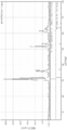
- FIG. 2 is an X-ray diffraction chart of an oxide sintered body produced in Example 1.
- FIG. 6 is an X-ray diffraction chart of an oxide sintered body produced in Example 6.
- FIG. 7 is an X-ray diffraction chart of an oxide sintered body produced in Example 7.
- the oxide sintered body of the present invention is an oxide sintered body containing indium element (In), gallium element (Ga), and tin element (Sn).
- the atomic ratio of each element satisfies the following formulas (1) to (3). 0.10 ⁇ In / (In + Ga + Sn) ⁇ 0.60 (1) 0.10 ⁇ Ga / (In + Ga + Sn) ⁇ 0.55 (2) 0.0001 ⁇ Sn / (In + Ga + Sn) ⁇ 0.60 (3)
- an oxide sintered body capable of forming an oxide semiconductor film suitable for a patterning process in manufacturing a semiconductor element can be obtained. Furthermore, an oxide sintered body having a low resistance and a high relative density, and an oxide sintered body having a good appearance with little color unevenness can be obtained.
- the atomic ratio of Sn and Ga preferably satisfies the following formulas (4) and (5), and more preferably satisfies the following formulas (8) and (9). In particular, it is preferable to satisfy the following formulas (10) and (11).
- wet etching can be performed with an organic acid etching solution (for example, oxalic acid etching solution), and it is difficult to dissolve in an inorganic acid wet etching solution (for example, a mixed acid wet etching solution of phosphoric acid / nitric acid / acetic acid).
- an organic acid etching solution for example, oxalic acid etching solution
- an inorganic acid wet etching solution for example, a mixed acid wet etching solution of phosphoric acid / nitric acid / acetic acid.
- the atomic ratio of Sn and Ga satisfies the above formulas (4), (5), (8) to (11), the atomic ratio of In is preferably in the range of the following formula. 0.40 ⁇ In / (In + Ga + Sn) ⁇ 0.60
- the atomic ratio of Sn satisfies the following formulas (6) and (7). 0.30 ⁇ Sn / (In + Ga + Sn) ⁇ 0.60 (6) 0.10 ⁇ In / (In + Ga + Sn) ⁇ 0.60 (7)
- the speed of dry etching is high, and the manufacturing speed can be increased when dry etching is used for forming a semiconductor layer.
- the higher the atomic ratio of the Sn element the faster the dry etching speed.
- the atomic ratio of the Sn element exceeds 0.60, a lower oxide of tin oxide is generated in the oxide semiconductor, and the characteristics are improved. May decrease.
- the atomic ratio of In and Ga is preferably in the range of the following formula. 0.20 ⁇ In / (In + Ga + Sn) ⁇ 0.40 0.20 ⁇ Ga / (In + Ga + Sn) ⁇ 0.40
- the content of zinc element (Zn) is preferably 10,000 ppm or less. That is, Zn may be included within a range not impairing the effects of the present invention.
- the content of Zn is more preferably 1000 ppm or less, and particularly preferably 100 ppm or less (substantially free).
- ppm means “atomic ppm”. Since the Zn content is small, there is an advantage that zinc does not diffuse into the Si substrate or the like even if heat treatment or the like is performed. Moreover, since the tolerance with respect to an inorganic acid improves, the etching selection ratio with Mo and Al with respect to an inorganic type wet etching liquid improves.
- the surface portion is less altered, and as a result, the thickness of the grinding can be reduced (the surface properties can be stabilized only by polishing without grinding). Furthermore, the difference between the surface and internal properties (crystal structure, resistance, particle size) is reduced.
- the metal element contained in the oxide sintered body may be substantially only In, Ga, and Sn.
- “substantially” means that the effect as a target is due to the composition of the metal element constituting the metal oxide sintered body, or the metal oxide constituting the metal oxide sintered body. It means that 95 wt% or more and 100 wt% or less (preferably 98 wt% or more and 100 wt% or less, particularly preferably 99.99 wt% or more and 100.00 wt% or less) is an oxide of the above metal element.
- the present invention may contain elements that are inevitably included in the refining process of raw materials that are usually available and impurities that are inevitably mixed in the process. It is preferable that the said element and the said impurity are 10 ppm or less with respect to all the structural components.
- the atomic ratio of each element contained in the oxide sintered body of the present invention can be determined by quantitative analysis of the contained elements using an inductively coupled plasma emission spectrometer (ICP-AES). Specifically, in the analysis using ICP-AES, when a solution sample is atomized with a nebulizer and introduced into an argon plasma (about 6000 to 8000 ° C.), the elements in the sample are excited by absorbing thermal energy, Orbital electrons move from the ground state to high energy level orbitals. These orbital electrons move to a lower energy level orbit in about 10 ⁇ 7 to 10 ⁇ 8 seconds. At this time, the energy difference is emitted as light to emit light. Since this light shows a wavelength (spectral line) unique to the element, the presence of the element can be confirmed by the presence or absence of the spectral line (qualitative analysis).
- ICP-AES inductively coupled plasma emission spectrometer
- the sample concentration can be obtained by comparing with a standard solution having a known concentration (quantitative analysis). After identifying the elements contained in the qualitative analysis, the content is obtained by qualitative analysis, and the atomic ratio of each element is obtained from the result.
- the oxide sintered body of the present invention preferably contains a compound having a crystal structure represented by Ga 3-x In 5 + x Sn 2 O 16 (wherein X is 0 to 1).
- Examples of the compound having a crystal structure represented by Ga 3-x In 5 + x Sn 2 O 16 include Ga 2 In 6 Sn 2 O 16 and Ga 2.4 In 5.6 Sn 2 O 16 .
- a compound having a crystal structure represented by Ga 3-x In 5 + x Sn 2 O 16 is referred to as a JCPDS (Joint Committee of Powder Diffraction Standards) card, and Ga 2 In 6 Sn 2 O 16 (JCPDS card: 51 ⁇ 0205) and Ga 2.4 In 5.6 Sn 2 O 16 (JCPDS card: 51-0204) or peak shift in the same pattern.
- JCPDS Joint Committee of Powder Diffraction Standards
- JCPDS card Ga 2 In 6 Sn 2 O 16
- JCPDS card Ga 2.4 In 5.6 Sn 2 O 16
- peak shift in the same pattern When the oxide sintered body of the present invention is analyzed by X-ray diffraction described later, (1) 30.0 to 32.0 °, (2) 35.0 to 37.0 °, (3) 51.0 to A peak exists in the range of 53.0 ° and (4) 60.5 to 63.0 °. Preferably, (1) 30.5-31.5 °, (2) 35.5-36.5 °, (3) 51.5-52.5 °, (4)
- the compound having a crystal structure represented by Ga 3 ⁇ x In 5 + x Sn 2 O 16 is desirably a main component or a second component. It is particularly desirable that it is a main component. Whether it is the main component or the second component is determined by the height of the peak obtained by X-ray diffraction described later. Specifically, the main component has the highest maximum peak intensity, and the second component has the maximum peak intensity next to the main component.
- An oxide sintered body containing a compound having a crystal structure represented by Ga 3-x In 5 + x Sn 2 O 16 exhibits characteristics such as low resistance and high density when used as a target.
- oxygen may be excessive or insufficient (oxygen deficiency). That is, they may be shifted according to the stoichiometric ratio. In the present invention, it preferably has an oxygen deficiency. If oxygen is excessive, the resistance may be too high when targeted.
- the oxide sintered body of the present invention is suitable for a sputtering target.
- the sputtering target (oxide sintered body) of the present invention can be obtained by a production method including the following steps (a) to (e).
- D A step of grinding the surface of the sintered body by 0.3 mm or more
- the compounding process is an essential process for mixing the metal oxide that is the raw material of the sputtering target.
- powders such as indium compound powder, gallium compound powder, and tin compound powder are used.
- the indium compound include indium oxide and indium hydroxide.
- the tin and gallium compounds include respective oxides and hydroxides.
- an oxide is preferable because it is easy to sinter and it is difficult to leave a by-product.
- the purity of the raw material is usually 2N (99% by mass) or more, preferably 3N (99.9% by mass) or more, particularly preferably 4N (99.99% by mass) or more.
- the purity is lower than 2N, the durability is deteriorated.
- impurities may enter the liquid crystal side and burning may occur. It is preferable to mix the raw materials used for the production of the target such as metal oxide and uniformly mix and pulverize them using an ordinary mixing and pulverizing machine such as a wet ball mill, a bead mill or an ultrasonic device.
- a calcination step may be provided before forming the raw material.
- a calcination process is a process provided as needed, after obtaining the mixture of the compound which is a raw material of a sputtering target, and calcining this mixture. Calcination makes it easy to increase the density of the obtained sintered body, which is preferable, but may increase the cost. Therefore, it is more preferable to increase the density without performing calcination.
- the raw material mixture is preferably heat-treated at 500 to 1200 ° C. for 1 to 100 hours. A heat treatment of less than 500 ° C. or less than 1 hour may result in insufficient thermal decomposition of the indium compound, gallium compound, and tin compound.
- the heat treatment condition exceeds 1200 ° C. or exceeds 100 hours, grain coarsening may occur.
- the calcination is particularly preferably carried out at a temperature range of 800 to 1200 ° C. for 2 to 50 hours.
- the calcined product obtained here is preferably pulverized before the following molding step and firing step.
- the molding process is an essential process for pressure-molding the raw material mixture (or calcined product when the calcining process is provided) to form a compact. By this process, it is formed into a shape suitable as a target.
- the obtained calcined fine powder can be granulated and then formed into a desired shape by press molding.
- the average thickness of the molded body is preferably 5.5 mm or more, more preferably 6 mm or more, further preferably 8 mm or more, and particularly preferably 12 mm or more. If it is 5.5 mm or more, the temperature gradient in the film thickness direction decreases, and it can be expected that the variation of the combination of the crystal form of the surface and the deep part is less likely to occur.
- Examples of the molding process that can be used in this step include press molding (uniaxial press), mold molding, cast molding, and injection molding.
- press molding uniaxial press
- mold molding cast molding
- injection molding In order to obtain a sintered body (target) having a high sintered density, it is preferable to perform molding by cold isostatic pressure (CIP) or the like.
- CIP cold isostatic pressure
- two or more stages of molding processes may be provided so as to be molded by cold isostatic pressure (CIP), hot isostatic pressure (HIP), or the like.
- CIP cold isostatic pressure
- HIP hot isostatic pressure
- the unevenness of the composition inside the molded body is reduced and uniformized. If the surface pressure is less than 800 kgf / cm 2 , the density after sintering may not increase or the resistance may increase. If the surface pressure exceeds 4000 kgf / cm 2 , the apparatus may become too large and uneconomical. If the holding time is less than 0.5 minutes, the density after sintering may not increase or the resistance may increase. If it exceeds 60 minutes, it may take too much time and it may be uneconomical. In addition, you may use shaping
- molding adjuvants such as polyvinyl alcohol, methylcellulose, polywax
- Sintering process is an essential process of baking the molded object obtained at the said formation process.
- As sintering conditions it is preferable to carry out under oxygen gas containing atmosphere, oxygen gas atmosphere, or oxygen gas pressurization. If sintering is performed in an atmosphere that does not contain oxygen gas, the density of the target obtained cannot be sufficiently improved, and the occurrence of abnormal discharge during sputtering may not be sufficiently suppressed.
- the heating rate up to the sintering temperature is preferably 3 ° C./min or less, more preferably 2.5 ° C./min or less, and particularly preferably 1.5 ° C./min or less. If the rate of temperature rise exceeds 3 ° C./min, the combination of the surface and deep crystal forms may vary. This is presumably because temperature unevenness occurs in the thickness direction of the target when the temperature is raised. Note that the temperature increase may be stopped once during the temperature increase and held at a predetermined temperature, and sintering may be performed in two or more stages.
- the sintering temperature is preferably from 1280 ° C to 1520 ° C, more preferably from 1300 ° C to 1500 ° C, and more preferably from 1320 ° C to 1480 ° C.
- the sintering time is preferably 2 hours to 96 hours, more preferably 4 hours to 48 hours, and particularly preferably 6 hours to 24 hours.
- the cooling rate during cooling is usually 4 ° C./min or less, preferably 2 ° C./min or less, more preferably 1 ° C./min or less, further preferably 0.8 ° C./min or less, particularly preferably 0.5 ° C./min. Is less than a minute.
- the crystal form of this invention is easy to be obtained as it is 4 degrees C / min or less. In addition, cracks are unlikely to occur when the temperature drops.
- a reduction treatment step may be provided in order to reduce the bulk resistance of the sintered body obtained in the sintering step as a whole.
- the reduction method include a method using a reducing gas, vacuum firing, or reduction using an inert gas.
- a reducing gas hydrogen, methane, carbon monoxide, a mixed gas of these gases and oxygen, or the like can be used.
- reduction treatment by firing in an inert gas nitrogen, argon, a mixed gas of these gases and oxygen, or the like can be used.
- the reduction treatment is performed, there is a possibility that a difference in resistance value between the surface portion and the deep portion is generated or amplified.
- the grinding (working) step is a step of cutting the sintered body obtained by sintering as described above into a shape suitable for mounting on a sputtering apparatus.
- the surface of the sintered body obtained in the step (c) is ground by 0.3 mm or more.
- the grinding depth is preferably 0.5 mm or more, particularly preferably 2 mm or more. If it is less than 0.3 mm, there is a possibility that the fluctuation part of the crystal structure near the surface cannot be removed.
- the sintered body is ground with, for example, a surface grinder to obtain a material having a surface roughness Ra of 5 ⁇ m or less.
- the sputtering surface of the sputtering target may be further mirror-finished so that the average surface roughness Ra is 1000 angstroms or less.
- a known polishing technique such as mechanical polishing, chemical polishing, mechanochemical polishing (a combination of mechanical polishing and chemical polishing) can be used.
- polishing to # 2000 or more with a fixed abrasive polisher polishing liquid: water
- lapping with loose abrasive lapping abrasive: SiC paste, etc.
- lapping by changing the abrasive to diamond paste can be obtained by:
- Such a polishing method is not particularly limited.
- Step (e): Bonding step This is a step of bonding the ground sintered body to the backing plate.
- cleaning, etc. can be used for the cleaning process of the oxide sintered compact after a grinding process.
- air blow running water washing
- ultrasonic cleaning or the like can be further performed. This ultrasonic cleaning is effective by performing multiple oscillations at a frequency of 25 to 300 KHz. For example, it is preferable to perform ultrasonic cleaning by multiplying twelve types of frequencies in 25 KHz increments between frequencies of 25 to 300 KHz.
- the sputtering target made of the oxide sintered body of the present invention preferably has a relative density of 85% or more, more preferably 92% or more, still more preferably 95% or more, and particularly preferably 97% or more. If the relative density of the sintered body is 85% or more, there is less risk of cracking or cracking when used as a sputtering target. In addition, the film forming speed is increased.
- the specific resistance is preferably 700 m ⁇ cm or less, more preferably 100 m ⁇ cm or less, further preferably 50 m ⁇ cm or less, and particularly preferably 20 m ⁇ cm or less.
- the film can be formed even when the sputtering power is lowered when used as a sputtering target. In particular, if it is 20 m ⁇ cm or less, there is little risk of cracking in the target even if DC sputtering is performed. Further, the number of aggregated portions of gallium oxide having a particle diameter of 2 ⁇ m or more in the oxide sintered body is preferably 10/8100 ⁇ m 2 or less.
- the oxide semiconductor thin film of the present invention can be formed.
- the oxide semiconductor film of the present invention contains each element of In, Ga, and Sn at an atomic ratio of the above formulas (1) to (3), and has an electron carrier density of 10 14 cm ⁇ 3 or more and 10 19 cm ⁇ 3 or less. It is.
- the oxide semiconductor film can be manufactured using the above-described sputtering target of the present invention and a known sputtering apparatus.
- the electron carrier density is evaluated using a Hall measuring device (for example, Resi Test 8310, manufactured by Toyo Technica).
- the Sn average valence measured by X-ray photoelectron spectroscopy (XPS) of the manufactured oxide semiconductor film is preferably +3.0 or more, more preferably +3.2 or more, particularly preferably +3.6 or more, +3 .8 or more is more preferable.
- the upper limit is usually +4.0.
- the Sn average valence is +3.0 or more, the TFT characteristics are improved, for example, the mobility increases when the TFT is manufactured.
- the band attributed to Sn5s is found only in the spectrum of SnO (Sn + 2: 4d 10 5s 2 electron configuration), which is a lower oxide, in SnO 2 (Sn + 4: 4d 10 electron configuration). Is not seen. Therefore, the Sn average valence can be obtained from the relative intensity of the Sn5s band (see: X-ray photoelectron spectroscopy, 1998, published by Maruzen Co., Ltd.). Usually, the Sn average valence of the SnO 2 film produced by sputtering is about +2.8.
- the composition ratio is within the range of the present invention, and the oxygen partial pressure is 2 ⁇ 10 ⁇ 3 Pa or more during sputtering. Further, the obtained film may be oxidized by exposing it to oxygen plasma.
- the oxide semiconductor thin film can be suitably used for various semiconductor elements.
- it can be suitably used as a semiconductor layer for a semiconductor layer, an oxide thin film layer, etc. of a thin film transistor.
- a thin film transistor will be described as an example of the semiconductor element.
- FIG. 1 a schematic cross-sectional view of a thin film transistor manufactured in this example is shown in FIG.
- This thin film transistor is a channel stopper type (inverted stagger type thin film transistor).
- a gate electrode 20 is sandwiched between a substrate 10 and a gate insulating film 30, and a channel layer (oxide semiconductor) 40 is stacked on the gate insulating film 30 as an active layer.
- a source electrode 50 and a drain electrode 52 are provided so as to cover the vicinity of the end of the semiconductor film 40.
- An etching stopper layer (protective film) 60 is formed in a portion surrounded by the semiconductor film 40, the source electrode 50 and the drain electrode 52.
- Substrate there is no particular limitation, and those known in this technical field can be used.
- glass substrates such as alkali silicate glass, non-alkali glass and quartz glass, silicon substrates, resin substrates such as acrylic, polycarbonate and polyethylene naphthalate (PEN), polymer film bases such as polyethylene terephthalate (PET) and polyamide Materials can be used.
- resin substrates such as acrylic, polycarbonate and polyethylene naphthalate (PEN), polymer film bases such as polyethylene terephthalate (PET) and polyamide Materials
- PET polyethylene terephthalate
- polyamide Materials can be used.
- a semiconductor layer consists of In, Sn, and Ga complex oxide.
- Such a semiconductor layer can be produced, for example, by forming a thin film using the sputtering target of the present invention. It can also be formed by a co-sputtering method, a PLD method (pulse laser deposition method), a sol-gel method, or the like using two or more types of targets having different compositions. Use of the sputtering target of the present invention is preferable because it is easy to industrialize.
- the semiconductor layer is preferably an amorphous film. By being an amorphous film, adhesion characteristics with an insulating film and a protective layer can be improved, and uniform transistor characteristics can be easily obtained even in a large area.
- whether the semiconductor layer is an amorphous film can be confirmed by X-ray crystal structure analysis. The case where no clear peak is observed is amorphous. Note that the amorphous material may contain microcrystals.
- the field effect transistor may have a protective layer of a semiconductor.
- the material for forming the semiconductor protective layer is not particularly limited. What is generally used can be arbitrarily selected as long as the effects of the present invention are not lost. For example, SiO 2, SiNx, Al 2 O 3, Ta 2 O 5, TiO 2, MgO, ZrO 2, CeO 2, K 2 O, Li 2 O, Na 2 O, Rb 2 O, Sc 2 O 3, Y 2 O 3 , Hf 2 O 3 , CaHfO 3 , PbTi 3 , BaTa 2 O 6 , SrTiO 3 , AlN, or the like can be used.
- Gate insulating film The material for forming the gate insulating film is not particularly limited. What is generally used can be arbitrarily selected as long as the effects of the invention of the present embodiment are not lost. For example, SiO 2, SiNx, Al 2 O 3, Ta 2 O 5, TiO 2, MgO, ZrO 2, CeO 2, K 2 O, Li 2 O, Na 2 O, Rb 2 O, Sc 2 O 3, Y 2 O 3 , Hf 2 O 3 , CaHfO 3 , PbTi 3 , BaTa 2 O 6 , SrTiO 3 , AlN, or the like can be used.
- the gate insulating film may be an organic insulating film such as poly (4-vinylphenol) (PVP) or parylene. Further, the gate insulating film may have a stacked structure of two or more layers of an inorganic insulating film and an organic insulating film.
- PVP poly (4-vinylphenol)
- Electrode There are no particular limitations on the material for forming each of the gate electrode, the source electrode, and the drain electrode, and any commonly used material can be selected as long as the effects of the present invention are not lost.
- transparent electrodes such as indium tin oxide (ITO), indium zinc oxide, ZnO, SnO 2 , metal electrodes such as Al, Ag, Cr, Ni, Mo, Au, Ti, Ta, Cu, or these An alloy metal electrode can be used.
- Each constituent member (layer) of the thin film transistor can be formed by a method known in this technical field.
- a film formation method a chemical film formation method such as a spray method, a dip method, or a CVD method, or a physical film formation method such as a sputtering method, a vacuum evaporation method, an ion plating method, or a pulse laser deposition method.
- the method can be used. Since the carrier density is easily controlled and the film quality can be easily improved, a physical film formation method is preferably used, and a sputtering method is more preferably used because of high productivity.
- the formed film can be patterned by various etching methods.
- the semiconductor layer is preferably formed by DC or AC sputtering using the target of the present invention.
- DC or AC sputtering damage during film formation can be reduced as compared with RF sputtering. For this reason, in the thin film transistor, an effect such as improvement in mobility can be expected.
- the heat treatment is preferably performed in an inert gas in an environment where the oxygen partial pressure is 10 ⁇ 3 Pa or less, or after the semiconductor layer is covered with a protective layer. Reproducibility is improved under the above conditions.
- the mobility is preferably not less than 3 cm 2 / Vs, more preferably at least 6 cm 2 / Vs, and particularly preferably equal to or greater than 10 cm 2 / Vs. If it is 3 cm 2 / Vs or more, the switching speed becomes faster, and it can be expected to be used for a large-screen high-definition display such as 4K2K.
- the on / off ratio is usually preferably 10 8 or more, more preferably 10 9 or more, and particularly preferably 10 10 or more. When the on / off ratio is high, the brightness and darkness of the image becomes clear, and an improvement in image quality can be expected.
- the off-current is usually 50 pA or less, preferably 10 pA or less, more preferably 5 pA or less, and particularly preferably 1 pA or less.
- the threshold voltage (Vth) is usually preferably ⁇ 1.0 to 3.0V, preferably ⁇ 0.5 to 2.0V, more preferably ⁇ 0.2 to 1.0V, and particularly preferably 0 to 0.5V. When the threshold voltage is within the above range, the drive voltage can be lowered and the power consumption can be reduced.
- Example 1 Production of oxide sintered body As starting materials, In 2 O 3 (purity 4N, BET surface area 15 m 2 / g), Ga 2 O 3 (purity 4N, BET surface area 15 m 2 / g) and SnO 2 (purity) 4N, BET surface area of 4 m 2 / g) was used. These raw materials were weighed so that the atomic ratio of the metal elements became the ratio of the oxide sintered body shown in Table 1, and mixed and ground using a ball mill. And after mixing and pulverizing, it was naturally dried. The obtained mixed powder was filled in a mold and pressure-molded with a press to produce a molded body having a thickness of 15 mm or more.
- the surface pressure at this time was 400 kgf / cm 2 and the holding time was 2 minutes. Then, it pressurized with CIP (hydrostatic-pressure pressurization apparatus). The surface pressure was 2000 kgf / cm 2 and held for 5 minutes. Thereafter, the obtained molded body was sintered in a sintering furnace.
- the sintering conditions were as follows. After sintering, it was naturally cooled to room temperature to obtain an oxide sintered body (thickness 9 mm). Temperature increase rate: 1 ° C / min Sintering temperature: 1400 ° C Sintering time: 12 hours Sintering atmosphere: Under air
- (D) Relative density (%) From the theoretical density calculated from the density of the raw material powder and the density of the sintered body measured by the Archimedes method, it was calculated by the following calculation formula. Relative density (%) (density measured by Archimedes method) ⁇ (theoretical density) ⁇ 100
- E Appearance (uneven color) The sintered bodies were visually observed from a location 50 cm away under daylight in the north window and classified as follows. A: Almost no color unevenness B: Some color unevenness C: Color unevenness In addition, when there is color unevenness in the sintered body, it may be difficult to judge the state when the target is used, for example.
- Etching rate of oxalic acid-based wet etching solution A Etching rate of 20 nm / min or more B: Etching rate of 5 nm / min or more and less than 20 nm / min C: Etching rate of less than 5 nm / min Resistance to phosphoric acid-based wet etching solution A: Etching rate 5 nm / min or less B: etching rate higher than 5 nm / min and 20 nm / min or less C: etching rate higher than 20 nm / min. Dry etching rate A: etching rate of 50 mm / min or more B: etching rate of less than 50 mm / min The Sn average valence measured by XPS of the thin film was +3.9.
- the channel stopper type thin film transistor (reverse stagger type thin film transistor) of FIG. 1 was produced and evaluated.
- the substrate 10 a glass substrate (Corning 1737) was used.
- 10 nm thick Mo, 80 nm thick Al, and 10 nm thick Mo were laminated in this order on the substrate 10 by electron beam evaporation.
- a laminated film was formed on the gate electrode 20 by using a photolithography method and a lift-off method.
- a 200 nm thick SiO 2 film was formed on the gate electrode 20 and the substrate 10 by the TEOS-CVD method to form the gate insulating layer 30.
- the substrate temperature is 50 ° C.
- the deposited oxide semiconductor film and protective film were processed into appropriate sizes by a photolithography method and an etching method. After the formation of the etching stopper layer 60, Mo having a thickness of 5 nm, Al having a thickness of 50 nm, and Mo having a thickness of 5 nm were laminated in this order, and the source electrode 50 and the drain electrode 52 were formed by photolithography and wet etching. . After that, heat treatment was performed in the atmosphere at 300 ° C. for 60 minutes, so that a transistor with a channel length of 20 ⁇ m and a channel width of 20 ⁇ m was manufactured.
- the mobility (field effect mobility ( ⁇ )), on / off ratio, off current, and threshold voltage (Vth) of the thin film transistor were measured.
- the measurement was performed using a semiconductor parameter analyzer (Keutley 4200) in a room temperature and light-shielded environment.
- Examples 2 to 9, Comparative Examples 1 to 5 An oxide sintered body and the like were prepared and evaluated in the same manner as in Example 1 except that the composition ratio of the oxide sintered body and the grinding amount were changed as shown in Tables 1 and 3.
- the results of X-ray diffraction measurement (XRD) of Examples 1, 6, 7, and 8 are shown in FIGS. 2 to 5, respectively.
- Table 4 shows the peak position (angle) read from the chart.
- Table 5 shows calculated values of “Each angle in Table 4 ⁇ Angle of peak (1) (circle 1 in FIG. 6)”. From the results of Table 5, it can be confirmed that the crystals have the same pattern and different interstitial distances having the same structure.
- Examples 10 and 11 As starting materials, In 2 O 3 (purity 4N, BET surface area 6 m 2 / g), Ga 2 O 3 (purity 4N, BET surface area 6 m 2 / g) and SnO 2 (purity 4N, BET surface area 6 m 2 / g) were used. used. These raw materials were weighed so that the atomic ratio of the metal elements was the ratio shown in Table 2, mixed with a super mixer, then packed in an alumina container, and calcined at 950 ° C. for 5 hours in an air atmosphere. did. Next, these raw materials were finely pulverized with an attritor ( ⁇ 3 mm zirconia beads, agitator rotation speed 300 rpm) for about 0.5 to 5 hours.
- an attritor ⁇ 3 mm zirconia beads, agitator rotation speed 300 rpm
- the finely pulverized slurry was dried with a spray dryer at 100 to 150 ° C. for 5 to 48 hours, and sieved with a sieve having an opening of 250 ⁇ m to collect powder.
- the fine pulverization was performed until the BET surface area became 10 m 2 / g or more.
- Table 2 the production conditions of the sintered body (presence / absence of calcining, mixing method, granulating method, sintering atmosphere, sintering temperature, sintering time, grinding amount, etc.) were changed.
- oxide sintered bodies and the like were prepared and evaluated.
- Example 12 As starting materials, In 2 O 3 (purity 4N, median diameter 1.8 ⁇ m), Ga 2 O 3 (purity 4N, median diameter 1.8 ⁇ m) and SnO 2 (purity 4N, median diameter 1.5 ⁇ m) were used. These raw materials were weighed so that the atomic ratio of the metal elements was the ratio shown in Table 2. The calcination was carried out in the same manner as in Example 10, and then pulverized until the median diameter of the mixed raw material became 1.0 ( ⁇ m). Hereinafter, oxide sintered bodies and the like were produced and evaluated in the same manner as in Example 10.
- Examples 13 to 16 A sputtering target was produced in the same manner as in Example 1 except that the composition ratio of the oxide sintered body was changed as shown in Table 2. A TFT was fabricated and evaluated in the same manner as in Example 1 except that dry etching was used when forming the semiconductor film.
- Examples 17-20 As starting materials, In 2 O 3 (purity 4N, median diameter 1.8 ⁇ m), Ga 2 O 3 (purity 4N, median diameter 1.8 ⁇ m) and SnO 2 (purity 4N, median diameter 1.5 ⁇ m) were used for oxidation.
- a sputtering target was produced in the same manner as in Example 10 except that the composition ratio of the sintered product and the sintering temperature were changed as shown in Table 2. Further, a TFT was produced and evaluated in the same manner as in Example 1.
- Examples 1 to 20 had less abnormal discharge.
- the Sn average valence measured by XPS in the same manner as in Example 1 was +3.1 in Example 16 and +2.8 in Comparative Example 1.
Abstract
Description
酸化物膜の成膜方法としては、スパッタリング、PLD(パルスレーザーデポジション)、蒸着等の物理的な成膜や、ゾルゲル法等の化学的な成膜が検討されている。比較的低温で大面積に均一に成膜できる方法として、スパッタリング法、PLD法、電子線ビーム蒸着法等の物理的成膜が中心に検討されている。物理的成膜法で酸化物薄膜を成膜する際は、均一に、安定して、効率よく、高い成膜速度で成膜するために、酸化物焼結体からなるターゲットを用いることが一般的である。特に、酸化物焼結体からなるターゲットをスパッタリング法に適用すると量産性に優れるため、フラットディスプレイ等大面積の用途に用いることができる。 An amorphous oxide film containing indium oxide is visible as a semiconductor film used for a transparent conductive film, a thin film transistor, and the like because it has visible light transmittance and wide electric characteristics from a conductor and a semiconductor to an insulator. ing.
As a method for forming an oxide film, physical film formation such as sputtering, PLD (pulse laser deposition), and vapor deposition, and chemical film formation such as a sol-gel method are being studied. As a method capable of forming a film uniformly over a large area at a relatively low temperature, physical film formation such as sputtering, PLD, and electron beam evaporation has been studied. When forming an oxide thin film by a physical film forming method, it is common to use a target made of an oxide sintered body in order to form a film uniformly, stably, efficiently, and at a high film forming speed. Is. In particular, when a target made of an oxide sintered body is applied to the sputtering method, it is excellent in mass productivity and can be used for a large area such as a flat display.
また、亜鉛元素を含むとシリコン基板上等のSi含有層上で種々の素子を作製する際、亜鉛元素がSi含有層内に拡散し、特性が劣化するという課題があり、適用できる素子構成が制限されていた。 On the other hand, in order to solve these problems, an oxide semiconductor film in which tin oxide is added to indium oxide, gallium oxide, and zinc oxide and a sputtering target for manufacturing the oxide semiconductor film are disclosed (Patent Document 3). However, the sputtering target made of indium oxide, gallium oxide, zinc oxide, and tin oxide has a problem that the number of elements to be managed is large and the manufacturing process and quality control are complicated.
In addition, when various elements are produced on a Si-containing layer such as a silicon substrate when zinc element is included, there is a problem that the zinc element diffuses into the Si-containing layer and the characteristics are deteriorated. It was restricted.
さらに、酸化錫の組成比を選定することで、ドライエッチングの際の選択比も向上できることを見出した。
さらに、Ga3-xIn5+xSn2O16(式中、Xは0~1である。)で表される結晶構造の化合物を含む製造条件を見出した。Ga3-xIn5+xSn2O16で表される結晶構造の化合物を含むことで、抵抗が低く密度が高くターゲットとして適した特性を持つ酸化物焼結体を得られることを見出した。 As a result of extensive research, the present inventor has increased the number of elements by using an oxide sintered body target having a composition containing tin oxide and not containing zinc oxide (composition composed of indium oxide, gallium oxide, and tin oxide). It was found that an oxide semiconductor film resistant to an inorganic acid-based wet etching solution (for example, a mixed acid wet etching solution of phosphoric acid / nitric acid / acetic acid) can be produced. Further, it has been found that a semiconductor film having characteristics equivalent to those of a semiconductor film made of indium oxide, gallium oxide, and zinc oxide can be produced with this target.
Furthermore, it has been found that the selection ratio during dry etching can be improved by selecting the composition ratio of tin oxide.
Furthermore, production conditions including a compound having a crystal structure represented by Ga 3-x In 5 + x Sn 2 O 16 (wherein X is 0 to 1) were found. It has been found that by including a compound having a crystal structure represented by Ga 3-x In 5 + x Sn 2 O 16 , an oxide sintered body having low resistance, high density and suitable characteristics as a target can be obtained.
1.インジウム元素(In)、ガリウム元素(Ga)及び錫元素(Sn)を、下記式(1)~(3)の原子比で含む酸化物焼結体。
0.10≦In/(In+Ga+Sn)≦0.60 (1)
0.10≦Ga/(In+Ga+Sn)≦0.55 (2)
0.0001<Sn/(In+Ga+Sn)≦0.60 (3)
2.前記In、Ga及びSnの原子比が下記式(4)及び(5)を満たす1に記載の酸化物焼結体。
0.01≦Sn/(In+Ga+Sn)≦0.30 (4)
0.30≦Ga/(In+Ga+Sn)≦0.55 (5)
3.前記In、Ga及びSnの原子比が下記式(6)及び(7)を満たす1に記載の酸化物焼結体。
0.30<Sn/(In+Ga+Sn)≦0.60 (6)
0.10≦In/(In+Ga+Sn)<0.60 (7)
4.亜鉛元素(Zn)の含有量が10000ppm以下である1~3のいずれかに記載の酸化物焼結体。
5.Ga3-xIn5+xSn2O16(式中、Xは0~1である。)で表される結晶構造の化合物を含む1~4のいずれかに記載の酸化物焼結体。
6.上記1~5のいずれかに記載の酸化物焼結体を用いたスパッタリングターゲット。
7.下記(a)~(e)の工程を含む6のスパッタリングターゲットの製造方法。
(a)原料化合物粉末を混合して混合物を調製する工程
(b)前記混合物を成形して平均厚み5.5mm以上の成形体を調製する工程
(c)前記成形体を1280℃以上1520℃以下で2時間以上96時間以下焼結する工程
(d)工程(c)で得た焼結体の表面を0.3mm以上研削する工程
(e)焼結体をバッキングプレートにボンディングする工程
8.インジウム元素(In)、ガリウム元素(Ga)及び錫元素(Sn)を、下記式(1)~(3)の原子比で含み、電子キャリア密度が1014cm-3以上1019cm-3以下である酸化物半導体膜。
0.10≦In/(In+Ga+Sn)≦0.60 (1)
0.10≦Ga/(In+Ga+Sn)≦0.55 (2)
0.0001<Sn/(In+Ga+Sn)≦0.60 (3)
9.上記8の酸化物半導体膜を用いた半導体素子。 According to the present invention, the following oxide sintered bodies and the like are provided.
1. An oxide sintered body containing indium element (In), gallium element (Ga), and tin element (Sn) in an atomic ratio of the following formulas (1) to (3).
0.10 ≦ In / (In + Ga + Sn) ≦ 0.60 (1)
0.10 ≦ Ga / (In + Ga + Sn) ≦ 0.55 (2)
0.0001 <Sn / (In + Ga + Sn) ≦ 0.60 (3)
2. 2. The oxide sintered body according to 1, wherein the atomic ratio of In, Ga, and Sn satisfies the following formulas (4) and (5).
0.01 ≦ Sn / (In + Ga + Sn) ≦ 0.30 (4)
0.30 ≦ Ga / (In + Ga + Sn) ≦ 0.55 (5)
3. 2. The oxide sintered body according to 1, wherein the atomic ratio of In, Ga, and Sn satisfies the following formulas (6) and (7).
0.30 <Sn / (In + Ga + Sn) ≦ 0.60 (6)
0.10 ≦ In / (In + Ga + Sn) <0.60 (7)
4). 4. The oxide sintered body according to any one of 1 to 3, wherein the content of zinc element (Zn) is 10,000 ppm or less.
5. 5. The oxide sintered body according to any one of 1 to 4, comprising a compound having a crystal structure represented by Ga 3-x In 5 + x Sn 2 O 16 (wherein X is 0 to 1).
6). 6. A sputtering target using the oxide sintered body according to any one of 1 to 5 above.
7). 6. A method for producing a sputtering target according to 6, comprising the following steps (a) to (e):
(A) A step of preparing a mixture by mixing raw material compound powders (b) A step of forming the mixture to prepare a molded body having an average thickness of 5.5 mm or more (c) 1280 ° C to 1520 ° C of the molded body (2) A step of grinding the surface of the sintered body obtained in step (c) by 0.3 mm or more (e) A step of bonding the sintered body to a backing plate. Indium element (In), gallium element (Ga), and tin element (Sn) are contained at an atomic ratio of the following formulas (1) to (3), and the electron carrier density is 10 14 cm −3 or more and 10 19 cm −3 or less. An oxide semiconductor film.
0.10 ≦ In / (In + Ga + Sn) ≦ 0.60 (1)
0.10 ≦ Ga / (In + Ga + Sn) ≦ 0.55 (2)
0.0001 <Sn / (In + Ga + Sn) ≦ 0.60 (3)
9. A semiconductor element using the oxide semiconductor film according to 8 above.
0.10≦In/(In+Ga+Sn)≦0.60 (1)
0.10≦Ga/(In+Ga+Sn)≦0.55 (2)
0.0001<Sn/(In+Ga+Sn)≦0.60 (3) The oxide sintered body of the present invention is an oxide sintered body containing indium element (In), gallium element (Ga), and tin element (Sn). The atomic ratio of each element satisfies the following formulas (1) to (3).
0.10 ≦ In / (In + Ga + Sn) ≦ 0.60 (1)
0.10 ≦ Ga / (In + Ga + Sn) ≦ 0.55 (2)
0.0001 <Sn / (In + Ga + Sn) ≦ 0.60 (3)
0.01≦Sn/(In+Ga+Sn)≦0.30 (4)
0.30≦Ga/(In+Ga+Sn)≦0.55 (5)
0.03≦Sn/(In+Ga+Sn)≦0.15 (8)
0.30<Ga/(In+Ga+Sn)≦0.50 (9)
0.04≦Sn/(In+Ga+Sn)≦0.11 (10)
0.32≦Ga/(In+Ga+Sn)≦0.48 (11) In the oxide sintered body of the present invention, the atomic ratio of Sn and Ga preferably satisfies the following formulas (4) and (5), and more preferably satisfies the following formulas (8) and (9). In particular, it is preferable to satisfy the following formulas (10) and (11).
0.01 ≦ Sn / (In + Ga + Sn) ≦ 0.30 (4)
0.30 ≦ Ga / (In + Ga + Sn) ≦ 0.55 (5)
0.03 ≦ Sn / (In + Ga + Sn) ≦ 0.15 (8)
0.30 <Ga / (In + Ga + Sn) ≦ 0.50 (9)
0.04 ≦ Sn / (In + Ga + Sn) ≦ 0.11 (10)
0.32 ≦ Ga / (In + Ga + Sn) ≦ 0.48 (11)
また、Sn/(In+Ga+Sn)を30原子%以下とすることにより、酸化錫の低級酸化物の生成(Sn平均価数の低下)によるトランジスタ性能の低下(移動度の低下、オンオフ比の低下)を避けることができる。15原子%以下だと、特に移動度やオンオフ比の向上が期待できる。
また、Ga/(In+Ga+Sn)を30原子%以上とすることで、透過率が向上し、TFTとした際に光劣化を抑えられることが期待できる。
尚、Sn及びGaの原子比が、上式(4)、(5)、(8)~(11)を満たす場合、Inの原子比は下記式の範囲が好ましい。
0.40≦In/(In+Ga+Sn)≦0.60 Within the above range, wet etching can be performed with an organic acid etching solution (for example, oxalic acid etching solution), and it is difficult to dissolve in an inorganic acid wet etching solution (for example, a mixed acid wet etching solution of phosphoric acid / nitric acid / acetic acid). The selectivity ratio of wet etching with Mo (molybdenum), Al (aluminum), etc. used in the process is large.
Further, by making Sn / (In + Ga + Sn) 30 atomic% or less, the transistor performance is lowered (the mobility is lowered and the on / off ratio is lowered) due to the formation of a lower oxide of tin oxide (lower Sn average valence). Can be avoided. When it is 15 atomic% or less, improvement in mobility and on / off ratio can be expected.
Further, by setting Ga / (In + Ga + Sn) to be 30 atomic% or more, it is expected that the transmittance is improved and that light deterioration can be suppressed when a TFT is formed.
When the atomic ratio of Sn and Ga satisfies the above formulas (4), (5), (8) to (11), the atomic ratio of In is preferably in the range of the following formula.
0.40 ≦ In / (In + Ga + Sn) ≦ 0.60
0.30<Sn/(In+Ga+Sn)≦0.60 (6)
0.10≦In/(In+Ga+Sn)<0.60 (7) In the oxide sintered body of the present invention, it is also preferable that the atomic ratio of Sn satisfies the following formulas (6) and (7).
0.30 <Sn / (In + Ga + Sn) ≦ 0.60 (6)
0.10 ≦ In / (In + Ga + Sn) <0.60 (7)
尚、Snの原子比が、上式(6)を満たす場合、In及びGaの原子比は下記式の範囲が好ましい。
0.20≦In/(In+Ga+Sn)≦0.40
0.20≦Ga/(In+Ga+Sn)≦0.40 When the atomic ratio of Sn is within the range of the formula (6), the speed of dry etching is high, and the manufacturing speed can be increased when dry etching is used for forming a semiconductor layer. The higher the atomic ratio of the Sn element, the faster the dry etching speed. However, when the atomic ratio of the Sn element exceeds 0.60, a lower oxide of tin oxide is generated in the oxide semiconductor, and the characteristics are improved. May decrease.
When the atomic ratio of Sn satisfies the above formula (6), the atomic ratio of In and Ga is preferably in the range of the following formula.
0.20 ≦ In / (In + Ga + Sn) ≦ 0.40
0.20 ≦ Ga / (In + Ga + Sn) ≦ 0.40
さらに、本発明は、通常入手可能な原料の精製工程上不可避的に含まれている元素やプロセス上不可避的に混入する不純物を含んでいてもよい。上記元素や上記不純物は、全構成成分に対して10ppm以下であることが好ましい。 In the present invention, the metal element contained in the oxide sintered body may be substantially only In, Ga, and Sn. Here, in the present application, “substantially” means that the effect as a target is due to the composition of the metal element constituting the metal oxide sintered body, or the metal oxide constituting the metal oxide sintered body. It means that 95 wt% or more and 100 wt% or less (preferably 98 wt% or more and 100 wt% or less, particularly preferably 99.99 wt% or more and 100.00 wt% or less) is an oxide of the above metal element.
Furthermore, the present invention may contain elements that are inevitably included in the refining process of raw materials that are usually available and impurities that are inevitably mixed in the process. It is preferable that the said element and the said impurity are 10 ppm or less with respect to all the structural components.
具体的に、ICP-AESを用いた分析では、溶液試料をネブライザーで霧状にして、アルゴンプラズマ(約6000~8000℃)に導入すると、試料中の元素は熱エネルギーを吸収して励起され、軌道電子が基底状態から高いエネルギー準位の軌道に移る。この軌道電子は10-7~10-8秒程度で、より低いエネルギー準位の軌道に移る。この際にエネルギーの差を光として放射し発光する。この光は元素固有の波長(スペクトル線)を示すため、スペクトル線の有無により元素の存在を確認できる(定性分析)。 The atomic ratio of each element contained in the oxide sintered body of the present invention can be determined by quantitative analysis of the contained elements using an inductively coupled plasma emission spectrometer (ICP-AES).
Specifically, in the analysis using ICP-AES, when a solution sample is atomized with a nebulizer and introduced into an argon plasma (about 6000 to 8000 ° C.), the elements in the sample are excited by absorbing thermal energy, Orbital electrons move from the ground state to high energy level orbitals. These orbital electrons move to a lower energy level orbit in about 10 −7 to 10 −8 seconds. At this time, the energy difference is emitted as light to emit light. Since this light shows a wavelength (spectral line) unique to the element, the presence of the element can be confirmed by the presence or absence of the spectral line (qualitative analysis).
定性分析で含有されている元素を特定後、定性分析で含有量を求め、その結果から各元素の原子比を求める。 In addition, since the magnitude (luminescence intensity) of each spectral line is proportional to the number of elements in the sample, the sample concentration can be obtained by comparing with a standard solution having a known concentration (quantitative analysis).
After identifying the elements contained in the qualitative analysis, the content is obtained by qualitative analysis, and the atomic ratio of each element is obtained from the result.
Ga3-xIn5+xSn2O16で表される結晶構造の化合物としては、Ga2In6Sn2O16やGa2.4In5.6Sn2O16等が挙げられる。Ga3-xIn5+xSn2O16で表される結晶構造の化合物であれば制限はない。
Ga3-xIn5+xSn2O16で表される結晶構造の化合物であることは、JCPDS(Joint Committee of Powder Diffraction Standards)カードと参照してGa2In6Sn2O16(JCPDSカード:51-0205)やGa2.4In5.6Sn2O16(JCPDSカード:51-0204)と一致する、あるいは同一のパターンでピークシフトしていることから判断する。
本発明の酸化物焼結体を後述のX線回析で分析すると、(1)30.0~32.0°、(2)35.0~37.0°、(3)51.0~53.0°、(4)60.5~63.0°の範囲にピークが存在する。好ましくは、(1)30.5~31.5°、(2)35.5~36.5°、(3)51.5~52.5°、(4)61.0~62.5°の範囲にピークが存在する。 The oxide sintered body of the present invention preferably contains a compound having a crystal structure represented by Ga 3-x In 5 + x Sn 2 O 16 (wherein X is 0 to 1).
Examples of the compound having a crystal structure represented by Ga 3-x In 5 + x Sn 2 O 16 include Ga 2 In 6 Sn 2 O 16 and Ga 2.4 In 5.6 Sn 2 O 16 . There is no limitation as long as the compound has a crystal structure represented by Ga 3-x In 5 + x Sn 2 O 16 .
A compound having a crystal structure represented by Ga 3-x In 5 + x Sn 2 O 16 is referred to as a JCPDS (Joint Committee of Powder Diffraction Standards) card, and Ga 2 In 6 Sn 2 O 16 (JCPDS card: 51 −0205) and Ga 2.4 In 5.6 Sn 2 O 16 (JCPDS card: 51-0204) or peak shift in the same pattern.
When the oxide sintered body of the present invention is analyzed by X-ray diffraction described later, (1) 30.0 to 32.0 °, (2) 35.0 to 37.0 °, (3) 51.0 to A peak exists in the range of 53.0 ° and (4) 60.5 to 63.0 °. Preferably, (1) 30.5-31.5 °, (2) 35.5-36.5 °, (3) 51.5-52.5 °, (4) 61.0-62.5 ° There is a peak in the range.
上記Ga3-xIn5+xSn2O16で表される結晶構造の化合物を含む酸化物焼結体は、ターゲットとして使用すると特に抵抗が低く密度が高いという特性を示す。 In the oxide sintered body of the present invention, the compound having a crystal structure represented by Ga 3−x In 5 + x Sn 2 O 16 is desirably a main component or a second component. It is particularly desirable that it is a main component. Whether it is the main component or the second component is determined by the height of the peak obtained by X-ray diffraction described later. Specifically, the main component has the highest maximum peak intensity, and the second component has the maximum peak intensity next to the main component.
An oxide sintered body containing a compound having a crystal structure represented by Ga 3-x In 5 + x Sn 2 O 16 exhibits characteristics such as low resistance and high density when used as a target.
装置:(株)リガク製Ultima-III
X線:Cu-Kα線(波長1.5406Å、グラファイトモノクロメータにて単色化)
2θ-θ反射法、連続スキャン(1.0°/分)
サンプリング間隔:0.02°
スリット DS、SS:2/3°、RS:0.6mm The measurement conditions of X-ray diffraction are as follows, for example.
Equipment: Ultimate-III manufactured by Rigaku Corporation
X-ray: Cu-Kα ray (wavelength 1.5406mm, monochromatized with graphite monochromator)
2θ-θ reflection method, continuous scan (1.0 ° / min)
Sampling interval: 0.02 °
Slit DS, SS: 2/3 °, RS: 0.6 mm
本発明のスパッタリングターゲット(酸化物焼結体)は、下記(a)~(e)の工程を含む製法により得ることができる。
(a)原料化合物粉末を混合して混合物を調製する工程
(b)前記混合物を成形して平均厚み5.5mm以上の成形体を調製する工程
(c)前記成形体を1280℃以上1520℃以下で2時間以上96時間以下焼結する工程
(d)焼結体の表面を0.3mm以上研削する工程
(e)焼結体をバッキングプレートにボンディングする工程 The oxide sintered body of the present invention is suitable for a sputtering target. Hereafter, the manufacturing method of the oxide sintered compact and sputtering target of this invention is demonstrated.
The sputtering target (oxide sintered body) of the present invention can be obtained by a production method including the following steps (a) to (e).
(A) A step of preparing a mixture by mixing raw material compound powders (b) A step of forming the mixture to prepare a molded body having an average thickness of 5.5 mm or more (c) 1280 ° C. or more and 1520 ° C. or less (D) A step of grinding the surface of the sintered body by 0.3 mm or more (e) A step of bonding the sintered body to the backing plate
配合工程は、スパッタリングターゲットの原料である金属酸化物を混合する必須の工程である。
原料としては、インジウム化合物の粉末、ガリウム化合物の粉末、スズ化合物の粉末等の粉末を用いる。インジウムの化合物としては、例えば、酸化インジウム、水酸化インジウム等が挙げられる。錫及びガリウムの化合物としては、例えば、それぞれの酸化物、水酸化物等が挙げられる。各々の化合物として、焼結のしやすさ、副生成物の残存のし難さから、酸化物が好ましい。
また、原料の純度は、通常2N(99質量%)以上、好ましくは3N(99.9質量%)以上、特に好ましくは4N(99.99質量%)以上である。純度が2Nより低いと耐久性が低下する、液晶ディスプレイに用いた際に液晶側に不純物が入り、焼き付けが起こるおそれがある。
金属酸化物等のターゲットの製造に用いる原料を混合し、通常の混合粉砕機、例えば、湿式ボールミルやビーズミル又は超音波装置を用いて、均一に混合・粉砕することが好ましい。 (1) Process (a): Compounding process The compounding process is an essential process for mixing the metal oxide that is the raw material of the sputtering target.
As the raw material, powders such as indium compound powder, gallium compound powder, and tin compound powder are used. Examples of the indium compound include indium oxide and indium hydroxide. Examples of the tin and gallium compounds include respective oxides and hydroxides. As each compound, an oxide is preferable because it is easy to sinter and it is difficult to leave a by-product.
The purity of the raw material is usually 2N (99% by mass) or more, preferably 3N (99.9% by mass) or more, particularly preferably 4N (99.99% by mass) or more. When the purity is lower than 2N, the durability is deteriorated. When used in a liquid crystal display, impurities may enter the liquid crystal side and burning may occur.
It is preferable to mix the raw materials used for the production of the target such as metal oxide and uniformly mix and pulverize them using an ordinary mixing and pulverizing machine such as a wet ball mill, a bead mill or an ultrasonic device.
仮焼により、得られる焼結体の密度を上げることが容易になり好ましいが、コストアップになるおそれがある。そのため、仮焼を行わずに密度を上げることがより好ましい。
仮焼工程においては、原料混合物を500~1200℃で、1~100時間熱処理することが好ましい。500℃未満又は1時間未満の熱処理では、インジウム化合物、ガリウム化合物、錫化合物の熱分解が不十分となる場合がある。一方、熱処理条件が、1200℃を超える場合又は100時間を超える場合には、粒子の粗大化が起こる場合がある。
仮焼は、特に、800~1200℃の温度範囲で、2~50時間実施することが好ましい。
尚、ここで得られた仮焼物は、下記の成形工程及び焼成工程の前に粉砕するのが好ましい。 In the present invention, a calcination step may be provided before forming the raw material. A calcination process is a process provided as needed, after obtaining the mixture of the compound which is a raw material of a sputtering target, and calcining this mixture.
Calcination makes it easy to increase the density of the obtained sintered body, which is preferable, but may increase the cost. Therefore, it is more preferable to increase the density without performing calcination.
In the calcination step, the raw material mixture is preferably heat-treated at 500 to 1200 ° C. for 1 to 100 hours. A heat treatment of less than 500 ° C. or less than 1 hour may result in insufficient thermal decomposition of the indium compound, gallium compound, and tin compound. On the other hand, when the heat treatment condition exceeds 1200 ° C. or exceeds 100 hours, grain coarsening may occur.
The calcination is particularly preferably carried out at a temperature range of 800 to 1200 ° C. for 2 to 50 hours.
The calcined product obtained here is preferably pulverized before the following molding step and firing step.
成形工程は、原料混合物(上記仮焼工程を設けた場合には仮焼物)を加圧成形して成形体とする必須の工程である。この工程により、ターゲットとして好適な形状に成形する。仮焼工程を設けた場合には、得られた仮焼物の微粉末を造粒した後、プレス成形により所望の形状に成形することができる。
成形体の平均厚みは5.5mm以上が好ましく、6mm以上がより好ましく、8mm以上がさらに好ましく、12mm以上が特に好ましい。5.5mm以上だと、膜厚方向の温度勾配が減少し、表面と深部の結晶型の組合せの変動が生じにくくなることが期待できる。 (2) Process (b): Molding process The molding process is an essential process for pressure-molding the raw material mixture (or calcined product when the calcining process is provided) to form a compact. By this process, it is formed into a shape suitable as a target. When the calcination step is provided, the obtained calcined fine powder can be granulated and then formed into a desired shape by press molding.
The average thickness of the molded body is preferably 5.5 mm or more, more preferably 6 mm or more, further preferably 8 mm or more, and particularly preferably 12 mm or more. If it is 5.5 mm or more, the temperature gradient in the film thickness direction decreases, and it can be expected that the variation of the combination of the crystal form of the surface and the deep part is less likely to occur.
また、プレス成形(一軸プレス)後に、冷間静水圧(CIP)、熱間静水圧(HIP)等で成形するように、2段階以上の成形工程を設けてもよい。
冷間静水圧、又は静水圧加圧装置を用いる場合、面圧800~4000kgf/cm2で0.5~60分保持することが好ましく、面圧2000~3000kgf/cm2で2~30分保持することがより好ましい。前記範囲内であると、成形体内部の組成むら等が減り、均一化されることが期待される。面圧が800kgf/cm2未満であると、焼結後の密度が上がらなかったり、抵抗が高くなるおそれがある。面圧4000kgf/cm2超であると、装置が大きくなりすぎ不経済となるおそれがある。保持時間が0.5分未満であると焼結後の密度が上がらなかったり、抵抗が高くなるおそれがある。60分超であると時間が掛かりすぎ不経済となるおそれがある。
尚、成形処理は、ポリビニルアルコールやメチルセルロース、ポリワックス、オレイン酸等の成形助剤を用いてもよい。 Examples of the molding process that can be used in this step include press molding (uniaxial press), mold molding, cast molding, and injection molding. In order to obtain a sintered body (target) having a high sintered density, it is preferable to perform molding by cold isostatic pressure (CIP) or the like.
Moreover, after press molding (uniaxial pressing), two or more stages of molding processes may be provided so as to be molded by cold isostatic pressure (CIP), hot isostatic pressure (HIP), or the like.
When using a cold isostatic pressure or a hydrostatic pressure press, it is preferable to hold at a surface pressure of 800 to 4000 kgf / cm 2 for 0.5 to 60 minutes, and at a surface pressure of 2000 to 3000 kgf / cm 2 for 2 to 30 minutes. More preferably. Within the above range, it is expected that the unevenness of the composition inside the molded body is reduced and uniformized. If the surface pressure is less than 800 kgf / cm 2 , the density after sintering may not increase or the resistance may increase. If the surface pressure exceeds 4000 kgf / cm 2 , the apparatus may become too large and uneconomical. If the holding time is less than 0.5 minutes, the density after sintering may not increase or the resistance may increase. If it exceeds 60 minutes, it may take too much time and it may be uneconomical.
In addition, you may use shaping | molding adjuvants, such as polyvinyl alcohol, methylcellulose, polywax | wax, oleic acid, for a shaping | molding process.
焼結工程は、上記成形工程で得られた成形体を焼成する必須の工程である。
焼結条件としては、酸素ガス含有雰囲気、酸素ガス雰囲気又は酸素ガス加圧下で行うことが好ましい。酸素ガスを含有しない雰囲気で焼結すると、得られるターゲットの密度を十分に向上させることができず、スパッタリング時の異常放電の発生を十分に抑制できなくなる場合がある。 (3) Process (c): Sintering process A sintering process is an essential process of baking the molded object obtained at the said formation process.
As sintering conditions, it is preferable to carry out under oxygen gas containing atmosphere, oxygen gas atmosphere, or oxygen gas pressurization. If sintering is performed in an atmosphere that does not contain oxygen gas, the density of the target obtained cannot be sufficiently improved, and the occurrence of abnormal discharge during sputtering may not be sufficiently suppressed.
尚、昇温の途中で一度昇温を止め所定の温度で保持し、2段階以上で焼結を行ってもよい。 The heating rate up to the sintering temperature is preferably 3 ° C./min or less, more preferably 2.5 ° C./min or less, and particularly preferably 1.5 ° C./min or less. If the rate of temperature rise exceeds 3 ° C./min, the combination of the surface and deep crystal forms may vary. This is presumably because temperature unevenness occurs in the thickness direction of the target when the temperature is raised.
Note that the temperature increase may be stopped once during the temperature increase and held at a predetermined temperature, and sintering may be performed in two or more stages.
焼結時間は、2時間以上96時間以下が好ましく、4時間以上48時間以下がより好ましく、6時間以上24時間以下が特に好ましい。 The sintering temperature is preferably from 1280 ° C to 1520 ° C, more preferably from 1300 ° C to 1500 ° C, and more preferably from 1320 ° C to 1480 ° C.
The sintering time is preferably 2 hours to 96 hours, more preferably 4 hours to 48 hours, and particularly preferably 6 hours to 24 hours.
還元性ガスによる還元処理の場合、水素、メタン、一酸化炭素や、これらのガスと酸素との混合ガス等を用いることができる。
不活性ガス中での焼成による還元処理の場合、窒素、アルゴンや、これらのガスと酸素との混合ガス等を用いることができる。
尚、本発明では、還元処理は行わないことが好ましい。還元処理を行うと、表面部と深部の抵抗値の違いを発生、又は増幅させるおそれがある。 In the present invention, a reduction treatment step may be provided in order to reduce the bulk resistance of the sintered body obtained in the sintering step as a whole. Examples of the reduction method include a method using a reducing gas, vacuum firing, or reduction using an inert gas.
In the case of reduction treatment with a reducing gas, hydrogen, methane, carbon monoxide, a mixed gas of these gases and oxygen, or the like can be used.
In the case of reduction treatment by firing in an inert gas, nitrogen, argon, a mixed gas of these gases and oxygen, or the like can be used.
In the present invention, it is preferable not to perform the reduction treatment. When the reduction treatment is performed, there is a possibility that a difference in resistance value between the surface portion and the deep portion is generated or amplified.
研削(加工)工程は、上記のようにして焼結して得られた焼結体を、スパッタリング装置への装着に適した形状に切削加工する工程である。
本発明では、上記工程(c)で得た焼結体の表面を0.3mm以上研削する。研削する深さは、0.5mm以上が好ましく、2mm以上が特に好ましい。0.3mm未満だと表面付近の結晶構造の変動部分を取り除けないおそれがある。 (4) Step (d): Grinding step The grinding (working) step is a step of cutting the sintered body obtained by sintering as described above into a shape suitable for mounting on a sputtering apparatus. .
In the present invention, the surface of the sintered body obtained in the step (c) is ground by 0.3 mm or more. The grinding depth is preferably 0.5 mm or more, particularly preferably 2 mm or more. If it is less than 0.3 mm, there is a possibility that the fluctuation part of the crystal structure near the surface cannot be removed.
研削後の焼結体をバッキングプレートにボンディングする工程である。
尚、研削工程後の酸化物焼結体の清浄処理には、エアーブローや流水洗浄等を使用できる。エアーブローで異物を除去する際には、ノズルの向い側から集塵機で吸気を行なうとより有効に除去できる。尚、エアーブローや流水洗浄では限界があるので、さらに超音波洗浄等を行なうこともできる。この超音波洗浄は周波数25~300KHzの間で多重発振させて行なう方法が有効である。例えば周波数25~300KHzの間で、25KHz刻みに12種類の周波数を多重発振させて超音波洗浄を行なうのがよい。 (5) Step (e): Bonding step This is a step of bonding the ground sintered body to the backing plate.
In addition, air blow, running water washing | cleaning, etc. can be used for the cleaning process of the oxide sintered compact after a grinding process. When removing foreign matter by air blow, it is possible to remove the foreign matter more effectively by suctioning with a dust collector from the opposite side of the nozzle. In addition, since there is a limit in air blow or running water cleaning, ultrasonic cleaning or the like can be further performed. This ultrasonic cleaning is effective by performing multiple oscillations at a frequency of 25 to 300 KHz. For example, it is preferable to perform ultrasonic cleaning by multiplying twelve types of frequencies in 25 KHz increments between frequencies of 25 to 300 KHz.
また、比抵抗は、700mΩcm以下が好ましく、100mΩcm以下がより好ましく、50mΩcm以下がさらに好ましく、20mΩcm以下が特に好ましい。焼結体の比抵抗が700mΩcm以下だとスパッタリングターゲットとして用いた時、スパッタ電力を下げても成膜することができる。特に20mΩcm以下だと、DCスパッタリングしてもターゲットにクラックが発生するおそれが少ない。
また、酸化物焼結体内部において、粒径2μm以上のガリウム酸化物の凝集部分の数が10個/8100μm2以下であることが好ましい。 The sputtering target made of the oxide sintered body of the present invention preferably has a relative density of 85% or more, more preferably 92% or more, still more preferably 95% or more, and particularly preferably 97% or more. If the relative density of the sintered body is 85% or more, there is less risk of cracking or cracking when used as a sputtering target. In addition, the film forming speed is increased.
The specific resistance is preferably 700 mΩcm or less, more preferably 100 mΩcm or less, further preferably 50 mΩcm or less, and particularly preferably 20 mΩcm or less. When the specific resistance of the sintered body is 700 mΩcm or less, the film can be formed even when the sputtering power is lowered when used as a sputtering target. In particular, if it is 20 mΩcm or less, there is little risk of cracking in the target even if DC sputtering is performed.
Further, the number of aggregated portions of gallium oxide having a particle diameter of 2 μm or more in the oxide sintered body is preferably 10/8100 μm 2 or less.
本発明の酸化物半導体膜は、In、Ga及びSnの各元素を、上記式(1)~(3)の原子比で含み、電子キャリア密度が1014cm-3以上1019cm-3以下である。酸化物半導体膜は、上述した本発明のスパッタリングターゲット、及び公知のスパッタリング装置を使用して作製できる。
電子キャリア密度は、ホール測定装置(例えば、東陽テクニカ製、Resi Test8310)を用いて評価する。
また、作製した酸化物半導体膜のX線光電子分光法(XPS)で測定したSn平均価数は、+3.0以上が好ましく、+3.2以上がより好ましく、+3.6以上が特に好ましく、+3.8以上がさらに好ましい。Sn平均価数は高いほど好ましいが、通常上限は+4.0である。
Sn平均価数は、+3.0以上であると、TFTを作製した際に、移動度が高くなる等TFTの特性が向上する。
XPS価電子帯スペクトルでは、Sn5sに起因するバンドは、低級酸化物であるSnO(Sn+2:4d105s2の電子配置)のスペクトルのみにみられ、SnO2(Sn+4:4d10の電子配置)にはみられない。そのため、Sn5sバンドの相対強度からSn平均価数を求めることができる(参照:X線光電子分光法、1998年、丸善株式会社刊)。通常、スパッタで作製したSnO2膜のSn平均価数は、+2.8程度である。
Sn平均価数を+3.0以上にするには、組成比を本発明の範囲内とし、スパッタリングの際に酸素分圧を2×10⁻³Pa以上とすると好ましい。また、得られた膜を酸素プラズマに曝す等で酸化させてもよい。 By sputtering the target such as a substrate using the sputtering target of the present invention, the oxide semiconductor thin film of the present invention can be formed.
The oxide semiconductor film of the present invention contains each element of In, Ga, and Sn at an atomic ratio of the above formulas (1) to (3), and has an electron carrier density of 10 14 cm −3 or more and 10 19 cm −3 or less. It is. The oxide semiconductor film can be manufactured using the above-described sputtering target of the present invention and a known sputtering apparatus.
The electron carrier density is evaluated using a Hall measuring device (for example, Resi Test 8310, manufactured by Toyo Technica).
The Sn average valence measured by X-ray photoelectron spectroscopy (XPS) of the manufactured oxide semiconductor film is preferably +3.0 or more, more preferably +3.2 or more, particularly preferably +3.6 or more, +3 .8 or more is more preferable. The higher the Sn average valence, the better. However, the upper limit is usually +4.0.
When the Sn average valence is +3.0 or more, the TFT characteristics are improved, for example, the mobility increases when the TFT is manufactured.
In the XPS valence band spectrum, the band attributed to Sn5s is found only in the spectrum of SnO (Sn + 2: 4d 10 5s 2 electron configuration), which is a lower oxide, in SnO 2 (Sn + 4: 4d 10 electron configuration). Is not seen. Therefore, the Sn average valence can be obtained from the relative intensity of the Sn5s band (see: X-ray photoelectron spectroscopy, 1998, published by Maruzen Co., Ltd.). Usually, the Sn average valence of the SnO 2 film produced by sputtering is about +2.8.
In order to set the Sn average valence to +3.0 or more, it is preferable that the composition ratio is within the range of the present invention, and the oxygen partial pressure is 2 × 10 −3 Pa or more during sputtering. Further, the obtained film may be oxidized by exposing it to oxygen plasma.
以下、半導体素子の例として、薄膜トランジスタについて説明する。 The oxide semiconductor thin film can be suitably used for various semiconductor elements. In particular, it can be suitably used as a semiconductor layer for a semiconductor layer, an oxide thin film layer, etc. of a thin film transistor.
Hereinafter, a thin film transistor will be described as an example of the semiconductor element.
特に制限はなく、本技術分野で公知のものを使用できる。例えば、ケイ酸アルカリ系ガラス、無アルカリガラス、石英ガラス等のガラス基板、シリコン基板、アクリル、ポリカーボネート、ポリエチレンナフタレート(PEN)等の樹脂基板、ポリエチレンテレフタレート(PET)、ポリアミド等の高分子フィルム基材等が使用できる。 (1) Substrate There is no particular limitation, and those known in this technical field can be used. For example, glass substrates such as alkali silicate glass, non-alkali glass and quartz glass, silicon substrates, resin substrates such as acrylic, polycarbonate and polyethylene naphthalate (PEN), polymer film bases such as polyethylene terephthalate (PET) and polyamide Materials can be used.
半導体層は、In、Sn及びGa複合酸化物からなる。このような半導体層は、例えば、本発明のスパッタリングターゲットを使用して薄膜を形成することで作製できる。2種以上の組成の異なるターゲットを用いたコスパッタ法、PLD法(パルスレーザーデポジション法)、ゾルゲル法等でも形成することができる。本発明のスパッタリングターゲットを用いることが、工業化が容易であり好ましい。
本発明において、半導体層は非晶質膜であることが好ましい。非晶質膜であることにより、絶縁膜や保護層との密着性が改善できる、大面積でも均一なトランジスタ特性が容易に得られることとなる。ここで、半導体層が非晶質膜であるかは、X線結晶構造解析により確認できる。明確なピークが観測されない場合が非晶質である。尚、非晶質中に微結晶が含まれていても構わない。 (2) Semiconductor layer A semiconductor layer consists of In, Sn, and Ga complex oxide. Such a semiconductor layer can be produced, for example, by forming a thin film using the sputtering target of the present invention. It can also be formed by a co-sputtering method, a PLD method (pulse laser deposition method), a sol-gel method, or the like using two or more types of targets having different compositions. Use of the sputtering target of the present invention is preferable because it is easy to industrialize.
In the present invention, the semiconductor layer is preferably an amorphous film. By being an amorphous film, adhesion characteristics with an insulating film and a protective layer can be improved, and uniform transistor characteristics can be easily obtained even in a large area. Here, whether the semiconductor layer is an amorphous film can be confirmed by X-ray crystal structure analysis. The case where no clear peak is observed is amorphous. Note that the amorphous material may contain microcrystals.
電界効果型トランジスタは、半導体の保護層を有していてもよい。半導体の保護層を形成する材料は特に制限はない。本発明の効果を失わない範囲で一般に用いられているものを任意に選択できる。例えば、SiO2,SiNx,Al2O3,Ta2O5,TiO2,MgO,ZrO2,CeO2,K2O,Li2O,Na2O,Rb2O,Sc2O3,Y2O3,Hf2O3,CaHfO3,PbTi3,BaTa2O6,SrTiO3,AlN等を用いることができる。これらのなかでも、SiO2,SiNx,Al2O3,Y2O3,Hf2O3,CaHfO3を用いるのが好ましく、より好ましくはSiO2,SiNx,Y2O3,Hf2O3,CaHfO3であり、特に好ましくはSiO2,Y2O3,Hf2O3,CaHfO3等の酸化物である。これらの酸化物の酸素数は、必ずしも化学量論比と一致していなくともよい(例えば、SiO2でもSiOxでもよい)。また、SiNxは水素元素を含んでいてもよい。
このような保護膜は、異なる2層以上の絶縁膜を積層した構造でもよい。 (3) Protective layer of semiconductor layer The field effect transistor may have a protective layer of a semiconductor. The material for forming the semiconductor protective layer is not particularly limited. What is generally used can be arbitrarily selected as long as the effects of the present invention are not lost. For example, SiO 2, SiNx, Al 2
Such a protective film may have a structure in which two or more different insulating films are stacked.
ゲート絶縁膜を形成する材料にも特に制限はない。本実施形態の発明の効果を失わない範囲で一般に用いられているものを任意に選択できる。例えば、SiO2,SiNx,Al2O3,Ta2O5,TiO2,MgO,ZrO2,CeO2,K2O,Li2O,Na2O,Rb2O,Sc2O3,Y2O3,Hf2O3,CaHfO3,PbTi3,BaTa2O6,SrTiO3,AlN等を用いることができる。これらのなかでも、SiO2,SiNx,Al2O3,Y2O3,Hf2O3,CaHfO3を用いるのが好ましく、より好ましくはSiO2,SiNx,Y2O3,Hf2O3,CaHfO3である。これらの酸化物の酸素数は、必ずしも化学量論比と一致していなくともよい(例えば、SiO2でもSiOxでもよい)。また、SiNxは水素元素を含んでいてもよい。
このようなゲート絶縁膜は、異なる2層以上の絶縁膜を積層した構造でもよい。また、ゲート絶縁膜は、結晶質、多結晶質、非晶質のいずれであってもよいが、工業的に製造しやすい多結晶質か、非晶質であるのが好ましい。
また、ゲート絶縁膜は、ポリ(4-ビニルフェノール)(PVP)、パリレン等の有機絶縁膜を用いてもよい。さらに、ゲート絶縁膜は無機絶縁膜及び有機絶縁膜の2層以上積層構造を有してもよい。 (4) Gate insulating film The material for forming the gate insulating film is not particularly limited. What is generally used can be arbitrarily selected as long as the effects of the invention of the present embodiment are not lost. For example, SiO 2, SiNx, Al 2
Such a gate insulating film may have a structure in which two or more different insulating films are stacked. The gate insulating film may be crystalline, polycrystalline, or amorphous, but is preferably polycrystalline or amorphous that is easy to manufacture industrially.
The gate insulating film may be an organic insulating film such as poly (4-vinylphenol) (PVP) or parylene. Further, the gate insulating film may have a stacked structure of two or more layers of an inorganic insulating film and an organic insulating film.
ゲート電極、ソ-ス電極及びドレイン電極の各電極を形成する材料に特に制限はなく、本発明の効果を失わない範囲で一般に用いられているものを任意に選択することができる。
例えば、インジウム錫酸化物(ITO)、インジウム亜鉛酸化物、ZnO、SnO2等の透明電極や、Al,Ag,Cr,Ni,Mo,Au,Ti,Ta、Cu等の金属電極、又はこれらを含む合金の金属電極を用いることができる。 (5) Electrode There are no particular limitations on the material for forming each of the gate electrode, the source electrode, and the drain electrode, and any commonly used material can be selected as long as the effects of the present invention are not lost. .
For example, transparent electrodes such as indium tin oxide (ITO), indium zinc oxide, ZnO, SnO 2 , metal electrodes such as Al, Ag, Cr, Ni, Mo, Au, Ti, Ta, Cu, or these An alloy metal electrode can be used.
形成した膜を各種エッチング法によりパターニングできる。
本発明では半導体層を、本発明のターゲットを用い、DC又はACスパッタリングにより成膜することが好ましい。DC又はACスパッタリングを用いることにより、RFスパッタリングの場合と比べて、成膜時のダメージを低減できる。このため、薄膜トランジスタにおいて、移動度の向上等の効果が期待できる。
また、本発明では半導体層と半導体の保護層を形成した後に、70~350℃で熱処理することが好ましい。70℃より低いと得られるトランジスタの熱安定性や耐熱性が低下したり、移動度が低くなったり、S値が大きくなったり、閾値電圧が高くなるおそれがある。一方、350℃より高いと耐熱性のない基板が使用できなかったり、熱処理用の設備費用がかかるおそれがある。
熱処理は、不活性ガス中で酸素分圧が10-3Pa以下の環境下で行うか、あるいは半導体層を保護層で覆った後に行うことが好ましい。上記条件下だと再現性が向上する。 Each constituent member (layer) of the thin film transistor can be formed by a method known in this technical field. Specifically, as a film formation method, a chemical film formation method such as a spray method, a dip method, or a CVD method, or a physical film formation method such as a sputtering method, a vacuum evaporation method, an ion plating method, or a pulse laser deposition method. The method can be used. Since the carrier density is easily controlled and the film quality can be easily improved, a physical film formation method is preferably used, and a sputtering method is more preferably used because of high productivity.
The formed film can be patterned by various etching methods.
In the present invention, the semiconductor layer is preferably formed by DC or AC sputtering using the target of the present invention. By using DC or AC sputtering, damage during film formation can be reduced as compared with RF sputtering. For this reason, in the thin film transistor, an effect such as improvement in mobility can be expected.
In the present invention, it is preferable to heat-treat at 70 to 350 ° C. after forming the semiconductor layer and the semiconductor protective layer. If it is lower than 70 ° C., the thermal stability and heat resistance of the obtained transistor may be lowered, the mobility may be lowered, the S value may be increased, or the threshold voltage may be increased. On the other hand, when the temperature is higher than 350 ° C., there is a possibility that a substrate having no heat resistance cannot be used or the cost of heat treatment equipment is increased.
The heat treatment is preferably performed in an inert gas in an environment where the oxygen partial pressure is 10 −3 Pa or less, or after the semiconductor layer is covered with a protective layer. Reproducibility is improved under the above conditions.
オンオフ比は、通常108以上が好ましく、109以上がより好ましく、1010以上が特に好ましい。オンオフ比が高いと、画像の明暗が明瞭になり画質の向上が期待できる。
オフ電流は通常50pA以下、10pA以下が好ましく、5pA以下がより好ましく、1pA以下が特に好ましい。オフ電流が50pA以下だと、リーク電流が少なくディスプレイのTFTに用いた場合に画質の向上が期待できる。
閾値電圧(Vth)は、通常-1.0~3.0V、-0.5~2.0Vが好ましく、-0.2~1.0Vがより好ましく、0~0.5Vが特に好ましい。閾値電圧が上記範囲内だと駆動電圧を下げることができ、消費電力を低減できる。 In the thin film transistor described above, the mobility is preferably not less than 3 cm 2 / Vs, more preferably at least 6 cm 2 / Vs, and particularly preferably equal to or greater than 10 cm 2 / Vs. If it is 3 cm 2 / Vs or more, the switching speed becomes faster, and it can be expected to be used for a large-screen high-definition display such as 4K2K.
The on / off ratio is usually preferably 10 8 or more, more preferably 10 9 or more, and particularly preferably 10 10 or more. When the on / off ratio is high, the brightness and darkness of the image becomes clear, and an improvement in image quality can be expected.
The off-current is usually 50 pA or less, preferably 10 pA or less, more preferably 5 pA or less, and particularly preferably 1 pA or less. When the off current is 50 pA or less, there is little leakage current, and an improvement in image quality can be expected when used for a TFT of a display.
The threshold voltage (Vth) is usually preferably −1.0 to 3.0V, preferably −0.5 to 2.0V, more preferably −0.2 to 1.0V, and particularly preferably 0 to 0.5V. When the threshold voltage is within the above range, the drive voltage can be lowered and the power consumption can be reduced.
(1)酸化物焼結体の作製
出発原料として、In2O3(純度4N、BET表面積15m2/g)、Ga2O3(純度4N、BET表面積15m2/g)及びSnO2(純度4N、BET表面積4m2/g)を使用した。
これらの原料を、金属元素の原子比が表1に示す酸化物焼結体の比となるように秤量し、ボールミルを使用して混合粉砕した。
そして混合粉砕後、自然乾燥させた。得られた混合粉末を金型に充填し、プレス機にて加圧成形して厚み15mm以上の成形体を作製した。尚、この際の面圧は400kgf/cm2とし、保持時間を2分とした。その後、CIP(静水圧加圧装置)にて加圧した。面圧は2000kgf/cm2とし、5分保持した。
その後、得られた成形体を焼結炉にて焼結した。焼結条件は以下のとおりとした。焼結後、室温まで自然冷却して酸化物焼結体(厚さ9mm)を得た。
昇温速度:1℃/分
焼結温度:1400℃
焼結時間:12時間
焼結雰囲気:大気下 Example 1
(1) Production of oxide sintered body As starting materials, In 2 O 3 (purity 4N, BET surface area 15 m 2 / g), Ga 2 O 3 (purity 4N, BET surface area 15 m 2 / g) and SnO 2 (purity) 4N, BET surface area of 4 m 2 / g) was used.
These raw materials were weighed so that the atomic ratio of the metal elements became the ratio of the oxide sintered body shown in Table 1, and mixed and ground using a ball mill.
And after mixing and pulverizing, it was naturally dried. The obtained mixed powder was filled in a mold and pressure-molded with a press to produce a molded body having a thickness of 15 mm or more. The surface pressure at this time was 400 kgf / cm 2 and the holding time was 2 minutes. Then, it pressurized with CIP (hydrostatic-pressure pressurization apparatus). The surface pressure was 2000 kgf / cm 2 and held for 5 minutes.
Thereafter, the obtained molded body was sintered in a sintering furnace. The sintering conditions were as follows. After sintering, it was naturally cooled to room temperature to obtain an oxide sintered body (thickness 9 mm).
Temperature increase rate: 1 ° C / min Sintering temperature: 1400 ° C
Sintering time: 12 hours Sintering atmosphere: Under air
焼結後、厚さ9mmの焼結体からスパッタリングターゲット用焼結体を切り出した。焼結体の上面、下面及び側辺をダイヤモンドカッターで切断し、表面を平面研削盤で研削して、厚さ5mmのターゲット素材とした。
次に、表面をエアーブローし、3分間超音波洗浄した。この後、ターゲット素材をインジウム半田にて無酸素銅製のバッキングプレートにボンディングしてターゲットとした。 (2) Production of sputtering target After sintering, a sintered body for sputtering target was cut out from a sintered body having a thickness of 9 mm. The upper surface, lower surface, and sides of the sintered body were cut with a diamond cutter, and the surface was ground with a surface grinder to obtain a target material having a thickness of 5 mm.
Next, the surface was blown with air and ultrasonically cleaned for 3 minutes. Thereafter, the target material was bonded to a backing plate made of oxygen-free copper with indium solder to obtain a target.
(A)組成
誘導プラズマ発光分析装置(ICP-AES)により原子比を分析した。
(B)結晶型
X線回折測定(XRD)にて焼結体及びその切断片を下記条件で直接測定した。
・装置:(株)リガク製Ultima-III
・X線:Cu-Kα線(波長1.5406Å、グラファイトモノクロメータにて単色化)
・2θ-θ反射法、連続スキャン(1.0°/分)
・サンプリング間隔:0.02°
・スリット DS、SS:2/3°、RS:0.6mm The following evaluation was performed about the obtained oxide sintered compact (target). The results are shown in Table 1.
(A) Composition The atomic ratio was analyzed with an induction plasma emission analyzer (ICP-AES).
(B) Crystal type The sintered body and its cut piece were directly measured under the following conditions by X-ray diffraction measurement (XRD).
・ Equipment: Ultimate-III manufactured by Rigaku Corporation
-X-ray: Cu-Kα ray (wavelength 1.5406mm, monochromatized with graphite monochromator)
・ 2θ-θ reflection method, continuous scan (1.0 ° / min)
・ Sampling interval: 0.02 °
・ Slit DS, SS: 2/3 °, RS: 0.6 mm
抵抗率計(三菱化学(株)製、ロレスタ)を使用し、四探針法(JIS R 1637)に基づき測定し、10箇所の平均値を抵抗率値とした。
(D)相対密度(%)
原料粉の密度から計算した理論密度と、アルキメデス法で測定した焼結体の密度から、下記計算式にて算出した。
相対密度(%)=(アルキメデス法で測定した密度)÷(理論密度)×100
(E)外観(色むら)
北窓昼光下、50cm離れた場所から焼結体を目視し、下記に分類した。
A:色むらがほとんどない
B:色むらが若干ある
C:色むらがある
尚、焼結体に色むらがある場合、例えばターゲットの使用時に状態の判断が難しくなるおそれがある。 (C) Resistivity A resistivity meter (manufactured by Mitsubishi Chemical Co., Ltd., Loresta) was used and measured based on the four-probe method (JIS R 1637), and the average value at 10 locations was defined as the resistivity value.
(D) Relative density (%)
From the theoretical density calculated from the density of the raw material powder and the density of the sintered body measured by the Archimedes method, it was calculated by the following calculation formula.
Relative density (%) = (density measured by Archimedes method) ÷ (theoretical density) × 100
(E) Appearance (uneven color)
The sintered bodies were visually observed from a
A: Almost no color unevenness B: Some color unevenness C: Color unevenness In addition, when there is color unevenness in the sintered body, it may be difficult to judge the state when the target is used, for example.
マグネトロンRFスパッタリングにより、全圧0.5Pa、酸素5%、アルゴン95%の条件で、100nmの酸化物膜を成膜して評価した。
有機酸として修酸系ウェットエッチング液(ITO-06N、関東化学(株)製)、無機酸としてリン酸系ウェットエッチング液(重量比で、H3PO4:73%、HNO3:3%、CH3COOH:7%、H2O:17%、に調整したもの)を用い、40℃におけるエッチング及び耐性を評価した。また、ドライエッチング速度を測定した。
評価は以下の通りとした。
・修酸系ウェットエッチング液エッチング速度
A:エッチング速度20nm/分以上
B:エッチング速度5nm/分以上20nm/分未満
C:エッチング速度5nm/分未満
・リン酸系ウェットエッチング液に対する耐性
A:エッチング速度5nm/分以下
B:エッチング速度5nm/分より速く20nm/分以下
C:エッチング速度20nm/分より速い
・ドライエッチング速度
A:エッチング速度50Å/分以上
B:エッチング速度50Å/分未満
また、得られた薄膜についてXPSで測定したSn平均価数は、+3.9であった。 (3) Fabrication and Evaluation of Thin Film A 100 nm oxide film was formed and evaluated by magnetron RF sputtering under conditions of a total pressure of 0.5 Pa, oxygen of 5%, and argon of 95%.
Oxidic acid-based wet etching solution (ITO-06N, manufactured by Kanto Chemical Co., Ltd.) as an organic acid, phosphoric acid-based wet etching solution (in weight ratio, H 3 PO 4 : 73%, HNO 3 : 3%, Etching and resistance at 40 ° C. were evaluated using CH 3 COOH: 7% and H 2 O: 17%. Also, the dry etching rate was measured.
Evaluation was as follows.
Etching rate of oxalic acid-based wet etching solution A: Etching rate of 20 nm / min or more B: Etching rate of 5 nm / min or more and less than 20 nm / min C: Etching rate of less than 5 nm / min Resistance to phosphoric acid-based wet etching solution A:
上記(2)で作製したスパッタリングターゲットを用いて、図1のチャンネルストッパー型薄膜トランジスタ(逆スタガ型薄膜トランジスタ)を作製し、評価した。
基板10は、ガラス基板(Corning1737)を用いた。まず、基板10上に電子ビーム蒸着法により、厚さ10nmのMoと厚さ80nmのAlと厚さ10nmのMoをこの順で積層した。積層膜をフォトリソグラフィー法とリフトオフ法を用いて、ゲート電極20に形成した。
ゲート電極20及び基板10上に、厚さ200nmのSiO2膜をTEOS-CVD法により成膜し、ゲート絶縁層30を形成した。尚、ゲート絶縁層の成膜はスパッタ法でもよいが、TEOS-CVD法やPECVD法等のCVD法で形成することが好ましい。スパッタ法ではオフ電流が高くなるおそれがある。
続いて、RFスパッタ法により、上記(2)で作製したターゲットを使用して、厚さ50nmの半導体膜40(チャネル層)を形成した。その後、大気中300℃で60分間熱処理した。
半導体膜40の上に、スパッタ法によりエッチングストッパー層60(保護膜)としてSiO2膜を堆積した。尚、保護膜の成膜方法はCVD法でもよい。
本実施例では、投入RFパワーは200Wとしている。成膜時の雰囲気は、全圧0.4Paであり、その際のガス流量比はAr:O2=95:5である。また、基板温度は50℃である。堆積させた酸化物半導体膜と保護膜は、フォトリソグラフィー法及びエッチング法により、適当な大きさに加工した。
エッチングストッパー層60の形成後に、厚さ5nmのMoと厚さ50nmのAlと厚さ5nmのMoをこの順で積層し、フォトリソグラフィー法とウェットエッチングにより、ソース電極50及びドレイン電極52を形成した。
その後、大気中300℃で60分間熱処理し、チャネル長が20μmで、チャネル幅が20μmのトランジスタを作製した。 (4) Production of Thin Film Transistor (TFT) Using the sputtering target produced in (2) above, the channel stopper type thin film transistor (reverse stagger type thin film transistor) of FIG. 1 was produced and evaluated.
As the
A 200 nm thick SiO 2 film was formed on the
Subsequently, a semiconductor film 40 (channel layer) having a thickness of 50 nm was formed by RF sputtering using the target prepared in (2) above. Then, it heat-processed for 60 minutes at 300 degreeC in air | atmosphere.
A SiO 2 film was deposited on the
In this embodiment, the input RF power is 200 W. The atmosphere during film formation is a total pressure of 0.4 Pa, and the gas flow rate ratio at that time is Ar: O 2 = 95: 5. The substrate temperature is 50 ° C. The deposited oxide semiconductor film and protective film were processed into appropriate sizes by a photolithography method and an etching method.
After the formation of the
After that, heat treatment was performed in the atmosphere at 300 ° C. for 60 minutes, so that a transistor with a channel length of 20 μm and a channel width of 20 μm was manufactured.
酸化物焼結体の組成比、及び研削量を表1及び表3に示すように変更した他は、実施例1と同様に酸化物焼結体等を作製し、評価した。
実施例1、6、7、8のX線回折測定(XRD)の結果を、それぞれ図2~5に示す。実施例1、6、7、8で作製した酸化物焼結体は、Ga3-xIn5+xSn2O16(Xは0~1である。)で表される結晶構造の化合物を含んでいることが確認できた。
また、実施例1,6,7,8のX線回折チャートの拡大図(2θ=28-38°、47-57°、57-67°)を、図6~8に示す。
表4に上記チャートから読み取ったピーク位置(角度)を示す。また、表5に「表4の各角度÷ピーク(1)(図6中の丸1)の角度」の計算値を示す。表5の結果から、パターンが一致し、同じ構造を持った格子間距離の異なった結晶であることが確認できる。 Examples 2 to 9, Comparative Examples 1 to 5
An oxide sintered body and the like were prepared and evaluated in the same manner as in Example 1 except that the composition ratio of the oxide sintered body and the grinding amount were changed as shown in Tables 1 and 3.
The results of X-ray diffraction measurement (XRD) of Examples 1, 6, 7, and 8 are shown in FIGS. 2 to 5, respectively. The oxide sintered bodies produced in Examples 1, 6, 7, and 8 include a compound having a crystal structure represented by Ga 3-x In 5 + x Sn 2 O 16 (X is 0 to 1). It was confirmed that
Further, enlarged views (2θ = 28-38 °, 47-57 °, 57-67 °) of the X-ray diffraction charts of Examples 1, 6, 7, and 8 are shown in FIGS.
Table 4 shows the peak position (angle) read from the chart. Table 5 shows calculated values of “Each angle in Table 4 ÷ Angle of peak (1) (
出発原料として、In2O3(純度4N、BET表面積6m2/g)、Ga2O3(純度4N、BET表面積6m2/g)及びSnO2(純度4N、BET表面積6m2/g)を使用した。
これらの原料を、金属元素の原子比が表2に示す比となるように秤量し、スーパーミキサーにて混合した後、これらをアルミナ製容器に詰め、大気雰囲気下で950℃、5時間仮焼した。次に、これらの原料をアトライター(φ3mmジルコニアビーズ、アジテーター回転数300rpm)にて0.5~5時間程度、微粉砕した。微粉砕後のスラリーをスプレードライヤーで、100~150℃×5~48時間乾燥し、目開き250μm篩で篩別して粉を回収した。尚、微粉砕は、BET表面積が10m2/g以上になるまで行なった。
以下、表2に示すように焼結体の作製条件(仮焼有無、混合方法、造粒方法、焼結雰囲気、焼結温度、焼結時間、研削量等)を変更した他は、実施例1と同様に酸化物焼結体等を作製し、評価した。 Examples 10 and 11
As starting materials, In 2 O 3 (purity 4N, BET surface area 6 m 2 / g), Ga 2 O 3 (purity 4N, BET surface area 6 m 2 / g) and SnO 2 (purity 4N, BET surface area 6 m 2 / g) were used. used.
These raw materials were weighed so that the atomic ratio of the metal elements was the ratio shown in Table 2, mixed with a super mixer, then packed in an alumina container, and calcined at 950 ° C. for 5 hours in an air atmosphere. did. Next, these raw materials were finely pulverized with an attritor (φ3 mm zirconia beads, agitator rotation speed 300 rpm) for about 0.5 to 5 hours. The finely pulverized slurry was dried with a spray dryer at 100 to 150 ° C. for 5 to 48 hours, and sieved with a sieve having an opening of 250 μm to collect powder. The fine pulverization was performed until the BET surface area became 10 m 2 / g or more.
Hereinafter, as shown in Table 2, the production conditions of the sintered body (presence / absence of calcining, mixing method, granulating method, sintering atmosphere, sintering temperature, sintering time, grinding amount, etc.) were changed. As in Example 1, oxide sintered bodies and the like were prepared and evaluated.
出発原料として、In2O3(純度4N、メジアン径1.8μm)、Ga2O3(純度4N、メジアン径1.8μm)及びSnO2(純度4N、メジアン径1.5μm)を使用した。これらの原料を、金属元素の原子比が表2に示す比となるように秤量した。
実施例10と同様に仮焼きし、その後、混合原料のメジアン径が1.0(μm)になるまで粉砕した。以下、実施例10と同様に酸化物焼結体等を作製し、評価した。 Example 12
As starting materials, In 2 O 3 (purity 4N, median diameter 1.8 μm), Ga 2 O 3 (purity 4N, median diameter 1.8 μm) and SnO 2 (purity 4N, median diameter 1.5 μm) were used. These raw materials were weighed so that the atomic ratio of the metal elements was the ratio shown in Table 2.
The calcination was carried out in the same manner as in Example 10, and then pulverized until the median diameter of the mixed raw material became 1.0 (μm). Hereinafter, oxide sintered bodies and the like were produced and evaluated in the same manner as in Example 10.
酸化物焼結体の組成比を表2に示すように変更した他は、実施例1と同様にスパッタリングターゲットを作製した。また、半導体膜の形成時にドライエッチングを用いた他は、実施例1と同様にTFTを作製し、評価した。 Examples 13 to 16
A sputtering target was produced in the same manner as in Example 1 except that the composition ratio of the oxide sintered body was changed as shown in Table 2. A TFT was fabricated and evaluated in the same manner as in Example 1 except that dry etching was used when forming the semiconductor film.
出発原料として、In2O3(純度4N、メジアン径1.8μm)、Ga2O3(純度4N、メジアン径1.8μm)及びSnO2(純度4N、メジアン径1.5μm)を用い、酸化物焼結体の組成比、焼結温度を表2に示すように変更した他は、実施例10と同様にスパッタリングターゲットを作製した。また、実施例1と同様にTFTを作製し、評価した。 Examples 17-20
As starting materials, In 2 O 3 (purity 4N, median diameter 1.8 μm), Ga 2 O 3 (purity 4N, median diameter 1.8 μm) and SnO 2 (purity 4N, median diameter 1.5 μm) were used for oxidation. A sputtering target was produced in the same manner as in Example 10 except that the composition ratio of the sintered product and the sintering temperature were changed as shown in Table 2. Further, a TFT was produced and evaluated in the same manner as in Example 1.
また、得られた薄膜について実施例1と同様にXPSで測定したSn平均価数は実施例16で+3.1、比較例1で+2.8であった。 In the above Examples and Comparative Examples, the number of aggregation portion having a particle diameter of 2μm or more gallium oxide, Examples 1 to 18 and 20 5 / 8100μm 2 or less, Example 19 8 / 8100μm 2, comparative In Examples 1 and 2, the number was 10 pieces / 8100 μm 2 or more. When sputtering was performed, Examples 1 to 20 had less abnormal discharge. On the other hand, abnormal discharges frequently occurred in Comparative Examples 1 and 2.
Further, the Sn average valence measured by XPS in the same manner as in Example 1 was +3.1 in Example 16 and +2.8 in Comparative Example 1.


この明細書に記載の文献の内容を全てここに援用する。 Although several embodiments and / or examples of the present invention have been described in detail above, those skilled in the art will recognize that these exemplary embodiments and / or embodiments are substantially without departing from the novel teachings and advantages of the present invention. It is easy to make many changes to the embodiment. Accordingly, many of these modifications are within the scope of the present invention.
The entire contents of the documents described in this specification are incorporated herein.
Claims (9)
- インジウム元素(In)、ガリウム元素(Ga)及び錫元素(Sn)を、下記式(1)~(3)の原子比で含む酸化物焼結体。
0.10≦In/(In+Ga+Sn)≦0.60 (1)
0.10≦Ga/(In+Ga+Sn)≦0.55 (2)
0.0001<Sn/(In+Ga+Sn)≦0.60 (3) An oxide sintered body containing indium element (In), gallium element (Ga), and tin element (Sn) in an atomic ratio of the following formulas (1) to (3).
0.10 ≦ In / (In + Ga + Sn) ≦ 0.60 (1)
0.10 ≦ Ga / (In + Ga + Sn) ≦ 0.55 (2)
0.0001 <Sn / (In + Ga + Sn) ≦ 0.60 (3) - 前記In、Ga及びSnの原子比が下記式(4)及び(5)を満たす請求項1に記載の酸化物焼結体。
0.01≦Sn/(In+Ga+Sn)≦0.30 (4)
0.30≦Ga/(In+Ga+Sn)≦0.55 (5) The oxide sintered body according to claim 1, wherein an atomic ratio of the In, Ga, and Sn satisfies the following formulas (4) and (5).
0.01 ≦ Sn / (In + Ga + Sn) ≦ 0.30 (4)
0.30 ≦ Ga / (In + Ga + Sn) ≦ 0.55 (5) - 前記In、Ga及びSnの原子比が下記式(6)及び(7)を満たす請求項1に記載の酸化物焼結体。
0.30<Sn/(In+Ga+Sn)≦0.60 (6)
0.10≦In/(In+Ga+Sn)<0.60 (7) The oxide sintered body according to claim 1, wherein an atomic ratio of the In, Ga, and Sn satisfies the following formulas (6) and (7).
0.30 <Sn / (In + Ga + Sn) ≦ 0.60 (6)
0.10 ≦ In / (In + Ga + Sn) <0.60 (7) - 亜鉛元素(Zn)の含有量が10000ppm以下である請求項1~3のいずれかに記載の酸化物焼結体。 The oxide sintered body according to any one of claims 1 to 3, wherein the content of zinc element (Zn) is 10,000 ppm or less.
- Ga3-xIn5+xSn2O16(式中、Xは0~1である。)で表される結晶構造の化合物を含む請求項1~4のいずれかに記載の酸化物焼結体。 The oxide sintered body according to any one of claims 1 to 4, comprising a compound having a crystal structure represented by Ga 3-x In 5 + x Sn 2 O 16 (wherein X is 0 to 1).
- 請求項1~5のいずれかに記載の酸化物焼結体を用いたスパッタリングターゲット。 A sputtering target using the oxide sintered body according to any one of claims 1 to 5.
- 下記(a)~(e)の工程を含む請求項6のスパッタリングターゲットの製造方法。
(a)原料化合物粉末を混合して混合物を調製する工程
(b)前記混合物を成形して平均厚み5.5mm以上の成形体を調製する工程
(c)前記成形体を1280℃以上1520℃以下で2時間以上96時間以下焼結する工程
(d)工程(c)で得た焼結体の表面を0.3mm以上研削する工程
(e)焼結体をバッキングプレートにボンディングする工程 The method for producing a sputtering target according to claim 6, comprising the following steps (a) to (e):
(A) A step of preparing a mixture by mixing raw material compound powders (b) A step of forming the mixture to prepare a molded body having an average thickness of 5.5 mm or more (c) 1280 ° C to 1520 ° C of the molded body (D) A step of grinding the surface of the sintered body obtained in step (c) by 0.3 mm or more (e) A step of bonding the sintered body to a backing plate - インジウム元素(In)、ガリウム元素(Ga)及び錫元素(Sn)を、下記式(1)~(3)の原子比で含み、電子キャリア密度が1014cm-3以上1019cm-3以下である酸化物半導体膜。
0.10≦In/(In+Ga+Sn)≦0.60 (1)
0.10≦Ga/(In+Ga+Sn)≦0.55 (2)
0.0001<Sn/(In+Ga+Sn)≦0.60 (3) Indium element (In), gallium element (Ga), and tin element (Sn) are contained at an atomic ratio of the following formulas (1) to (3), and the electron carrier density is 10 14 cm −3 or more and 10 19 cm −3 or less. An oxide semiconductor film.
0.10 ≦ In / (In + Ga + Sn) ≦ 0.60 (1)
0.10 ≦ Ga / (In + Ga + Sn) ≦ 0.55 (2)
0.0001 <Sn / (In + Ga + Sn) ≦ 0.60 (3) - 請求項8の酸化物半導体膜を用いた半導体素子。 A semiconductor element using the oxide semiconductor film according to claim 8.
Priority Applications (4)
| Application Number | Priority Date | Filing Date | Title |
|---|---|---|---|
| KR1020127022054A KR101840062B1 (en) | 2010-02-24 | 2011-02-22 | In-Ga-Sn OXIDE SINTER, TARGET, OXIDE SEMICONDUCTOR FILM, AND SEMICONDUCTOR ELEMENT |
| CN201180010725.3A CN102770577B (en) | 2010-02-24 | 2011-02-22 | In-Ga-Sn oxide sintered body, target, oxide semiconductor film, and semiconductor element |
| US13/580,355 US8999208B2 (en) | 2010-02-24 | 2011-02-22 | In-Ga-Sn oxide sinter, target, oxide semiconductor film, and semiconductor element |
| KR1020187007154A KR20180030725A (en) | 2010-02-24 | 2011-02-22 | In-Ga-Sn OXIDE SINTER, TARGET, OXIDE SEMICONDUCTOR FILM, AND SEMICONDUCTOR ELEMENT |
Applications Claiming Priority (2)
| Application Number | Priority Date | Filing Date | Title |
|---|---|---|---|
| JP2010038979A JP2011174134A (en) | 2010-02-24 | 2010-02-24 | In-Ga-Sn-BASED OXIDE SINTERED COMPACT, TARGET, OXIDE SEMICONDUCTOR FILM AND SEMICONDUCTOR ELEMENT |
| JP2010-038979 | 2010-02-24 |
Publications (1)
| Publication Number | Publication Date |
|---|---|
| WO2011105047A1 true WO2011105047A1 (en) | 2011-09-01 |
Family
ID=44506480
Family Applications (1)
| Application Number | Title | Priority Date | Filing Date |
|---|---|---|---|
| PCT/JP2011/000972 WO2011105047A1 (en) | 2010-02-24 | 2011-02-22 | In-Ga-Sn OXIDE SINTER, TARGET, OXIDE SEMICONDUCTOR FILM, AND SEMICONDUCTOR ELEMENT |
Country Status (6)
| Country | Link |
|---|---|
| US (1) | US8999208B2 (en) |
| JP (1) | JP2011174134A (en) |
| KR (2) | KR101840062B1 (en) |
| CN (2) | CN102770577B (en) |
| TW (1) | TWI553134B (en) |
| WO (1) | WO2011105047A1 (en) |
Cited By (6)
| Publication number | Priority date | Publication date | Assignee | Title |
|---|---|---|---|---|
| WO2013027391A1 (en) * | 2011-08-22 | 2013-02-28 | 出光興産株式会社 | In-ga-sn based oxide sintered compact |
| US20130320336A1 (en) * | 2012-05-31 | 2013-12-05 | Samsung Corning Precision Materials Co., Ltd. | Oxide Semiconductor Sputtering Target, Method Of Manufacturing Thin-Film Transistors Using The Same, And Thin Film Transistor Manufactured Using The Same |
| WO2015080271A1 (en) * | 2013-11-29 | 2015-06-04 | 株式会社コベルコ科研 | Sintered oxide and sputtering target, and method for producing same |
| WO2015122417A1 (en) * | 2014-02-14 | 2015-08-20 | 株式会社コベルコ科研 | Sintered oxide and sputtering target |
| JP2016111324A (en) * | 2014-09-02 | 2016-06-20 | 株式会社神戸製鋼所 | Thin film transistor |
| JP2020122173A (en) * | 2019-01-29 | 2020-08-13 | Jx金属株式会社 | Sputtering target member, sputtering target, method of manufacturing sputter film, method of manufacturing film body, lamination structure, method of manufacturing lamination structure, organic el device, and method of manufacturing organic el device |
Families Citing this family (18)
| Publication number | Priority date | Publication date | Assignee | Title |
|---|---|---|---|---|
| CN102593161B (en) * | 2007-03-20 | 2014-11-05 | 出光兴产株式会社 | Semiconductor device with a plurality of transistors |
| US9331206B2 (en) * | 2011-04-22 | 2016-05-03 | Semiconductor Energy Laboratory Co., Ltd. | Oxide material and semiconductor device |
| JP5301021B2 (en) * | 2011-09-06 | 2013-09-25 | 出光興産株式会社 | Sputtering target |
| KR101893992B1 (en) * | 2011-12-15 | 2018-08-31 | 삼성코닝어드밴스드글라스 유한회사 | Thin film transistor having active layer consisting of five component material and display device having the same |
| WO2013108630A1 (en) * | 2012-01-18 | 2013-07-25 | 出光興産株式会社 | Field-effect transistor |
| KR101405257B1 (en) * | 2012-05-31 | 2014-06-10 | 삼성코닝어드밴스드글라스 유한회사 | Oxide semiconductor target, and method of manufacturing thin-film transistor using the same |
| JP2014225626A (en) * | 2012-08-31 | 2014-12-04 | 株式会社神戸製鋼所 | Thin film transistor and display |
| KR102090289B1 (en) | 2013-05-30 | 2020-04-16 | 삼성디스플레이 주식회사 | Oxide sputtering target, thin film transistor using the same and method for manufacturing thin film transistor |
| US10252507B2 (en) * | 2013-11-19 | 2019-04-09 | Rofin-Sinar Technologies Llc | Method and apparatus for forward deposition of material onto a substrate using burst ultrafast laser pulse energy |
| TWI545777B (en) * | 2014-01-15 | 2016-08-11 | Kobe Steel Ltd | Thin film transistor |
| JP2016225505A (en) * | 2015-06-01 | 2016-12-28 | 株式会社神戸製鋼所 | Thin film transistor, method of manufacturing the same, and sputtering target |
| WO2017122618A1 (en) * | 2016-01-15 | 2017-07-20 | 住友化学株式会社 | Method for preparing amorphous composite metal oxide |
| JP6875088B2 (en) | 2016-02-26 | 2021-05-19 | 株式会社神戸製鋼所 | Thin film transistor including oxide semiconductor layer |
| KR102382130B1 (en) * | 2017-02-01 | 2022-04-01 | 이데미쓰 고산 가부시키가이샤 | Oxide semiconductor film, thin film transistor, oxide sintered body, and sputtering target |
| US11251310B2 (en) | 2017-02-22 | 2022-02-15 | Idemitsu Kosan Co., Ltd. | Oxide semiconductor film, electronic device comprising thin film transistor, oxide sintered body and sputtering target |
| CN111448336B (en) * | 2017-12-28 | 2022-03-01 | 三井金属矿业株式会社 | Oxide sintered body, sputtering target, and oxide thin film |
| JP6834062B2 (en) * | 2018-08-01 | 2021-02-24 | 出光興産株式会社 | Crystal structure compounds, oxide sintered bodies, and sputtering targets |
| CN116813310A (en) * | 2023-06-01 | 2023-09-29 | 先导薄膜材料(广东)有限公司 | Rare earth element doped indium tin gallium oxide target material and preparation method thereof |
Citations (4)
| Publication number | Priority date | Publication date | Assignee | Title |
|---|---|---|---|---|
| JP2000077358A (en) * | 1998-08-27 | 2000-03-14 | Asahi Glass Co Ltd | Transparent conductive film, sputtering target and basic body with transparent conductive film |
| JP2008280216A (en) * | 2007-05-11 | 2008-11-20 | Idemitsu Kosan Co Ltd | In-Ga-Zn-Sn-BASED OXIDE SINTERED COMPACT, AND TARGET FOR PHYSICAL FILM DEPOSITION |
| WO2009128424A1 (en) * | 2008-04-16 | 2009-10-22 | 住友金属鉱山株式会社 | Thin film transistor type substrate, thin film transistor type liquid crystal display device and method for manufacturing thin film transistor type substrate |
| JP2010118407A (en) * | 2008-11-11 | 2010-05-27 | Idemitsu Kosan Co Ltd | Thin-film transistor having etching resistance, and production method thereof |
Family Cites Families (10)
| Publication number | Priority date | Publication date | Assignee | Title |
|---|---|---|---|---|
| JPH04272612A (en) | 1991-02-26 | 1992-09-29 | Kojundo Chem Lab Co Ltd | Transparent electrode |
| JPH0794015A (en) | 1993-06-30 | 1995-04-07 | Chichibu Onoda Cement Corp | Composition for manufacturing conductor |
| US5407602A (en) * | 1993-10-27 | 1995-04-18 | At&T Corp. | Transparent conductors comprising gallium-indium-oxide |
| JP4403591B2 (en) | 1998-10-29 | 2010-01-27 | 東ソー株式会社 | Conductive metal oxide sintered body and use thereof |
| JP5098151B2 (en) | 2005-10-31 | 2012-12-12 | 凸版印刷株式会社 | Thin film transistor manufacturing method |
| JP4318689B2 (en) | 2005-12-09 | 2009-08-26 | 出光興産株式会社 | N-type inorganic semiconductor, n-type inorganic semiconductor thin film, and manufacturing method thereof |
| WO2009075281A1 (en) | 2007-12-13 | 2009-06-18 | Idemitsu Kosan Co., Ltd. | Field effect transistor using oxide semiconductor and method for manufacturing the same |
| JP4765051B2 (en) * | 2008-01-16 | 2011-09-07 | Dowaエレクトロニクス株式会社 | Tin-doped indium oxide powder |
| US8455371B2 (en) | 2008-05-22 | 2013-06-04 | Idemitsu Kosan Co., Ltd. | Sputtering target, method for forming amorphous oxide thin film using the same, and method for manufacturing thin film transistor |
| JPWO2010018707A1 (en) * | 2008-08-11 | 2012-01-26 | 出光興産株式会社 | Gallium oxide-tin oxide based oxide sintered body and oxide film |
-
2010
- 2010-02-24 JP JP2010038979A patent/JP2011174134A/en active Pending
-
2011
- 2011-02-22 US US13/580,355 patent/US8999208B2/en active Active
- 2011-02-22 CN CN201180010725.3A patent/CN102770577B/en active Active
- 2011-02-22 KR KR1020127022054A patent/KR101840062B1/en active IP Right Grant
- 2011-02-22 KR KR1020187007154A patent/KR20180030725A/en not_active Application Discontinuation
- 2011-02-22 CN CN201610292859.3A patent/CN105924137B/en active Active
- 2011-02-22 WO PCT/JP2011/000972 patent/WO2011105047A1/en active Application Filing
- 2011-02-24 TW TW100106273A patent/TWI553134B/en active
Patent Citations (4)
| Publication number | Priority date | Publication date | Assignee | Title |
|---|---|---|---|---|
| JP2000077358A (en) * | 1998-08-27 | 2000-03-14 | Asahi Glass Co Ltd | Transparent conductive film, sputtering target and basic body with transparent conductive film |
| JP2008280216A (en) * | 2007-05-11 | 2008-11-20 | Idemitsu Kosan Co Ltd | In-Ga-Zn-Sn-BASED OXIDE SINTERED COMPACT, AND TARGET FOR PHYSICAL FILM DEPOSITION |
| WO2009128424A1 (en) * | 2008-04-16 | 2009-10-22 | 住友金属鉱山株式会社 | Thin film transistor type substrate, thin film transistor type liquid crystal display device and method for manufacturing thin film transistor type substrate |
| JP2010118407A (en) * | 2008-11-11 | 2010-05-27 | Idemitsu Kosan Co Ltd | Thin-film transistor having etching resistance, and production method thereof |
Cited By (11)
| Publication number | Priority date | Publication date | Assignee | Title |
|---|---|---|---|---|
| WO2013027391A1 (en) * | 2011-08-22 | 2013-02-28 | 出光興産株式会社 | In-ga-sn based oxide sintered compact |
| US20130320336A1 (en) * | 2012-05-31 | 2013-12-05 | Samsung Corning Precision Materials Co., Ltd. | Oxide Semiconductor Sputtering Target, Method Of Manufacturing Thin-Film Transistors Using The Same, And Thin Film Transistor Manufactured Using The Same |
| JP2013249537A (en) * | 2012-05-31 | 2013-12-12 | Samsung Corning Precision Materials Co Ltd | Oxide semiconductor sputtering target, and manufacturing method of thin film transistor using the same |
| CN103451607A (en) * | 2012-05-31 | 2013-12-18 | 三星康宁精密素材株式会社 | Oxide semiconductor sputtering target, thin-film transistor manufactured by the same and manufacturing method thereof |
| US9224820B2 (en) * | 2012-05-31 | 2015-12-29 | Samsung Corning Advanced Glass, Llc | Oxide semiconductor sputtering target, method of manufacturing thin-film transistors using the same, and thin film transistor manufactured using the same |
| WO2015080271A1 (en) * | 2013-11-29 | 2015-06-04 | 株式会社コベルコ科研 | Sintered oxide and sputtering target, and method for producing same |
| CN105246855A (en) * | 2013-11-29 | 2016-01-13 | 株式会社钢臂功科研 | Sintered oxide and sputtering target, and method for producing same |
| US10515787B2 (en) | 2013-11-29 | 2019-12-24 | Kobelco Research Institute, Inc. | Oxide sintered body and sputtering target, and method for producing same |
| WO2015122417A1 (en) * | 2014-02-14 | 2015-08-20 | 株式会社コベルコ科研 | Sintered oxide and sputtering target |
| JP2016111324A (en) * | 2014-09-02 | 2016-06-20 | 株式会社神戸製鋼所 | Thin film transistor |
| JP2020122173A (en) * | 2019-01-29 | 2020-08-13 | Jx金属株式会社 | Sputtering target member, sputtering target, method of manufacturing sputter film, method of manufacturing film body, lamination structure, method of manufacturing lamination structure, organic el device, and method of manufacturing organic el device |
Also Published As
| Publication number | Publication date |
|---|---|
| JP2011174134A (en) | 2011-09-08 |
| CN102770577A (en) | 2012-11-07 |
| TW201137135A (en) | 2011-11-01 |
| TWI553134B (en) | 2016-10-11 |
| CN105924137A (en) | 2016-09-07 |
| KR20130027007A (en) | 2013-03-14 |
| CN102770577B (en) | 2016-06-08 |
| CN105924137B (en) | 2020-02-18 |
| US8999208B2 (en) | 2015-04-07 |
| KR101840062B1 (en) | 2018-03-19 |
| KR20180030725A (en) | 2018-03-23 |
| US20120313057A1 (en) | 2012-12-13 |
Similar Documents
| Publication | Publication Date | Title |
|---|---|---|
| WO2011105047A1 (en) | In-Ga-Sn OXIDE SINTER, TARGET, OXIDE SEMICONDUCTOR FILM, AND SEMICONDUCTOR ELEMENT | |
| JP6389545B2 (en) | In-Ga-Sn oxide sintered body | |
| JP6314198B2 (en) | Composite oxide sintered body and sputtering target comprising the same | |
| JP5690063B2 (en) | In-Ga-Zn-based oxide sintered sputtering target and thin film transistor | |
| JP5894015B2 (en) | Composite oxide sintered body and sputtering target comprising the same | |
| TWI506153B (en) | Sputtering target and the use of its thin film transistor | |
| WO2011040028A1 (en) | SINTERED In-Ga-Zn-O-TYPE OXIDE | |
| WO2009148154A1 (en) | Sputtering target for oxide thin film and process for producing the sputtering target | |
| WO2014073210A1 (en) | Sputtering target, oxide semiconductor thin film, and methods for producing these products | |
| JP5990167B2 (en) | Sputtering target and manufacturing method thereof, and oxide thin film, thin film transistor and display device manufacturing method using the target | |
| JP4891381B2 (en) | In-Ga-Zn-based sintered body and sputtering target | |
| WO2012153494A1 (en) | Thin-film transistor | |
| JP5762204B2 (en) | Sputtering target, oxide semiconductor thin film, and manufacturing method thereof | |
| JP6141381B2 (en) | Manufacturing method of sputtering target | |
| JP6389541B2 (en) | In-Ga-Sn-based oxide sintered body, target, oxide semiconductor film, and semiconductor element | |
| JP2012056842A (en) | In-Ga-Zn OXIDE, OXIDE SINTERED COMPACT, AND SPUTTERING TARGET |
Legal Events
| Date | Code | Title | Description |
|---|---|---|---|
| WWE | Wipo information: entry into national phase |
Ref document number: 201180010725.3 Country of ref document: CN |
|
| 121 | Ep: the epo has been informed by wipo that ep was designated in this application |
Ref document number: 11747019 Country of ref document: EP Kind code of ref document: A1 |
|
| WWE | Wipo information: entry into national phase |
Ref document number: 13580355 Country of ref document: US |
|
| ENP | Entry into the national phase |
Ref document number: 20127022054 Country of ref document: KR Kind code of ref document: A |
|
| NENP | Non-entry into the national phase |
Ref country code: DE |
|
| 122 | Ep: pct application non-entry in european phase |
Ref document number: 11747019 Country of ref document: EP Kind code of ref document: A1 |