WO2011104962A1 - 液晶表示パネル - Google Patents
液晶表示パネル Download PDFInfo
- Publication number
- WO2011104962A1 WO2011104962A1 PCT/JP2010/071278 JP2010071278W WO2011104962A1 WO 2011104962 A1 WO2011104962 A1 WO 2011104962A1 JP 2010071278 W JP2010071278 W JP 2010071278W WO 2011104962 A1 WO2011104962 A1 WO 2011104962A1
- Authority
- WO
- WIPO (PCT)
- Prior art keywords
- layer
- transparent colored
- spacer
- transparent
- liquid crystal
- Prior art date
- Legal status (The legal status is an assumption and is not a legal conclusion. Google has not performed a legal analysis and makes no representation as to the accuracy of the status listed.)
- Ceased
Links
Images











Classifications
-
- G—PHYSICS
- G02—OPTICS
- G02F—OPTICAL DEVICES OR ARRANGEMENTS FOR THE CONTROL OF LIGHT BY MODIFICATION OF THE OPTICAL PROPERTIES OF THE MEDIA OF THE ELEMENTS INVOLVED THEREIN; NON-LINEAR OPTICS; FREQUENCY-CHANGING OF LIGHT; OPTICAL LOGIC ELEMENTS; OPTICAL ANALOGUE/DIGITAL CONVERTERS
- G02F1/00—Devices or arrangements for the control of the intensity, colour, phase, polarisation or direction of light arriving from an independent light source, e.g. switching, gating or modulating; Non-linear optics
- G02F1/01—Devices or arrangements for the control of the intensity, colour, phase, polarisation or direction of light arriving from an independent light source, e.g. switching, gating or modulating; Non-linear optics for the control of the intensity, phase, polarisation or colour
- G02F1/13—Devices or arrangements for the control of the intensity, colour, phase, polarisation or direction of light arriving from an independent light source, e.g. switching, gating or modulating; Non-linear optics for the control of the intensity, phase, polarisation or colour based on liquid crystals, e.g. single liquid crystal display cells
- G02F1/133—Constructional arrangements; Operation of liquid crystal cells; Circuit arrangements
- G02F1/1333—Constructional arrangements; Manufacturing methods
- G02F1/1335—Structural association of cells with optical devices, e.g. polarisers or reflectors
- G02F1/133509—Filters, e.g. light shielding masks
- G02F1/133514—Colour filters
-
- G—PHYSICS
- G02—OPTICS
- G02F—OPTICAL DEVICES OR ARRANGEMENTS FOR THE CONTROL OF LIGHT BY MODIFICATION OF THE OPTICAL PROPERTIES OF THE MEDIA OF THE ELEMENTS INVOLVED THEREIN; NON-LINEAR OPTICS; FREQUENCY-CHANGING OF LIGHT; OPTICAL LOGIC ELEMENTS; OPTICAL ANALOGUE/DIGITAL CONVERTERS
- G02F1/00—Devices or arrangements for the control of the intensity, colour, phase, polarisation or direction of light arriving from an independent light source, e.g. switching, gating or modulating; Non-linear optics
- G02F1/01—Devices or arrangements for the control of the intensity, colour, phase, polarisation or direction of light arriving from an independent light source, e.g. switching, gating or modulating; Non-linear optics for the control of the intensity, phase, polarisation or colour
- G02F1/13—Devices or arrangements for the control of the intensity, colour, phase, polarisation or direction of light arriving from an independent light source, e.g. switching, gating or modulating; Non-linear optics for the control of the intensity, phase, polarisation or colour based on liquid crystals, e.g. single liquid crystal display cells
- G02F1/133—Constructional arrangements; Operation of liquid crystal cells; Circuit arrangements
- G02F1/1333—Constructional arrangements; Manufacturing methods
- G02F1/1339—Gaskets; Spacers; Sealing of cells
- G02F1/13394—Gaskets; Spacers; Sealing of cells spacers regularly patterned on the cell subtrate, e.g. walls, pillars
-
- G—PHYSICS
- G02—OPTICS
- G02F—OPTICAL DEVICES OR ARRANGEMENTS FOR THE CONTROL OF LIGHT BY MODIFICATION OF THE OPTICAL PROPERTIES OF THE MEDIA OF THE ELEMENTS INVOLVED THEREIN; NON-LINEAR OPTICS; FREQUENCY-CHANGING OF LIGHT; OPTICAL LOGIC ELEMENTS; OPTICAL ANALOGUE/DIGITAL CONVERTERS
- G02F1/00—Devices or arrangements for the control of the intensity, colour, phase, polarisation or direction of light arriving from an independent light source, e.g. switching, gating or modulating; Non-linear optics
- G02F1/01—Devices or arrangements for the control of the intensity, colour, phase, polarisation or direction of light arriving from an independent light source, e.g. switching, gating or modulating; Non-linear optics for the control of the intensity, phase, polarisation or colour
- G02F1/13—Devices or arrangements for the control of the intensity, colour, phase, polarisation or direction of light arriving from an independent light source, e.g. switching, gating or modulating; Non-linear optics for the control of the intensity, phase, polarisation or colour based on liquid crystals, e.g. single liquid crystal display cells
- G02F1/133—Constructional arrangements; Operation of liquid crystal cells; Circuit arrangements
- G02F1/136—Liquid crystal cells structurally associated with a semi-conducting layer or substrate, e.g. cells forming part of an integrated circuit
- G02F1/1362—Active matrix addressed cells
- G02F1/136222—Colour filters incorporated in the active matrix substrate
Definitions
- the present invention relates to a liquid crystal display panel. More specifically, the present invention relates to a liquid crystal display panel using a color filter laminate as a spacer.
- a liquid crystal display (LCD: Liquid Crystal Display) device has a configuration in which a liquid crystal layer is sandwiched between a pair of substrates, and a voltage is applied to the liquid crystal layer by an electrode formed on the substrate to change the alignment state of liquid crystal molecules. Display is performed by changing the polarization state of light transmitted through the liquid crystal layer.
- a pair of substrates sandwiching the liquid crystal layer is held at a constant interval (cell gap) by a spacer, and is bonded to each other by a sealing material.
- a spacer for example, a transparent bead-shaped one can be mentioned, but a columnar spacer may be used because the contrast may be lowered if the dispersed spacer becomes non-uniform (for example, patent document). See 1-6.)
- color filters of a plurality of colors such as red, green, and blue are formed in the pixel opening region, and at the same time, color filters of each color are applied to a plurality of predetermined locations on the black matrix.
- a convex portion in which three color filters of red, green, and blue are stacked is formed, and the convex portion is used as a columnar spacer (see, for example, Patent Documents 7 to 9).
- a pair of substrates sandwiching a liquid crystal layer is composed of an array substrate having switching elements such as electrodes, wirings, TFTs (Thin Film Transistors) for applying a voltage to the liquid crystal layer, and color display.
- switching elements such as electrodes, wirings, TFTs (Thin Film Transistors) for applying a voltage to the liquid crystal layer, and color display.
- TFTs Thin Film Transistors
- Each of the color filter substrate and the color filter substrate having a black matrix or the like is configured as a separate substrate.
- JP-A-8-195138 Japanese Patent Laid-Open No. 61-110227 Japanese Utility Model Publication No. 4-48518 JP 61-165916 A Japanese Utility Model Publication No. 7-56177 Japanese Utility Model Publication No. 3-263014 JP-A-10-177109 JP 2003-156751 A JP 2006-30907 A JP 2001-117085 A
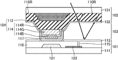
- FIG. 25 is a schematic diagram showing a cross section when a columnar spacer (hereinafter also referred to as a laminated spacer) formed by laminating a color filter, a black matrix, or the like in a conventional liquid crystal display panel.
- the liquid crystal display panel shown in FIG. 25 has an array substrate 101, a color filter substrate 102, and a liquid crystal layer 103 disposed therebetween.
- the array substrate 101 has various wirings such as a gate wiring 121, a source wiring, and a drain wiring 122, and TFTs connected to these wirings on a support substrate 111 made of glass or the like.
- the insulating layers 116 are isolated from each other.
- a plurality of pixel electrodes 113 are arranged on the interlayer insulating layer 116, and each of the pixel electrodes 113 is connected to a drain wiring 122 for supplying a predetermined signal via a contact hole 115 provided in the interlayer insulating layer 116. It is connected. As a result, the pixel electrodes 113 are individually charged with electric charges.
- the color filter substrate 102 has color filters of each color facing each pixel electrode 113 with the liquid crystal layer 103 interposed therebetween, and has a black matrix (BM) in the gap between the color filters.
- the laminated spacer 104 is provided on the support substrate 131 on the color filter substrate 102 side, and from the support substrate 131 side, the black matrix 112, the red (R) color filter 114R, the green (G) color filter 114G, and , Blue (B) color filters 114B are laminated in this order.
- the common electrode 132 covers the entire surface of the multilayer spacer 104, and a cap insulating layer 117 is provided on the common electrode 132.
- the color filter substrate 102 has a support substrate 131, a laminated spacer 104, a common electrode 132, and a cap insulating layer 117 laminated in this order toward the liquid crystal layer 103.
- the common electrode 132 covering the entire surface of the laminated spacer 104 is formed simultaneously with the common electrode formed on the color filter in the pixel opening region.
- the cap insulating layer 117 formed on the common electrode 132 is an insulating layer formed to prevent the common electrode 132 of the color filter substrate 102 and the pixel electrode 113 of the array substrate 101 from conducting.
- the present inventors have made various studies on the use of a laminated spacer in which a color filter, a black matrix, etc. are laminated as a spacer for holding a distance between a pair of substrates that sandwich a liquid crystal layer. Then, as described above, it is possible to prevent conduction by forming a cap insulating layer on the common electrode, but an extra manufacturing process such as a coating process and a patterning process of the cap insulating layer is necessary. We paid attention to the point. In addition, it may be possible to prevent conduction by patterning so that a part of the pixel electrode is removed in a region where the laminated spacer is in contact with the array substrate. However, consideration is given to a deviation that occurs when the pair of substrates is bonded. It was necessary to pay attention to the point that the opening area of the pixel opening region can be lost because the electrode having an area larger than the area where the laminated spacer is in contact with the array substrate has to be removed.
- the present invention has been made in view of the above situation, and prevents the occurrence of an electrical short circuit (leakage) between a pair of substrates without increasing the number of manufacturing steps when using a laminated spacer. It is an object of the present invention to provide a liquid crystal display panel that can be used.
- the inventors focused on the point that the laminated spacer was provided on the color filter substrate side, and the entire laminated spacer had to be covered with the common electrode in the manufacturing process. If the laminated spacer is provided on the array substrate side, the pixel electrode needs to be patterned on the array substrate, so that it is not necessary to form the pixel electrode on the entire laminated spacer without increasing the number of steps.
- the electrodes provided on each of the pair of substrates can be prevented from causing a short circuit (leakage), and the above problem can be solved brilliantly.
- the present invention has been achieved.
- the present invention is a liquid crystal display panel having a pair of substrates and a liquid crystal layer sandwiched between the pair of substrates, wherein one of the pair of substrates includes a support substrate, a plurality of pixel electrodes, and the above A plurality of transparent colored layers overlapping with a plurality of pixel electrodes; and a stacked spacer including three or more resin layers including a plurality of transparent colored layers, the other of the pair of substrates being a supporting substrate And a common electrode.
- liquid crystal display panel of the present invention will be described in detail below.
- the liquid crystal display panel of the present invention includes a pair of substrates and a liquid crystal layer sandwiched between the pair of substrates.
- members such as electrodes, wiring, and switching elements on one or both of the pair of substrates to control the orientation of the liquid crystal molecules in the liquid crystal layer, the polarization state of the light transmitted through the liquid crystal layer can be changed and desired Image display can be obtained.
- One of the pair of substrates includes a support substrate, a plurality of pixel electrodes, a plurality of transparent coloring layers overlapping with the plurality of pixel electrodes, and a plurality of transparent coloring layers. And a laminated spacer containing three or more resin layers.
- the liquid crystal display panel of the present invention is a form of a so-called color filter on array, and an array substrate is provided with both a plurality of transparent colored layers and a plurality of pixel electrodes.
- the color filter-on-array structure allows a larger alignment margin, simplifies the manufacturing process, and reduces the pixel aperture ratio compared to when the transparent colored layer and the pixel electrode are provided on separate substrates. Will also expand.
- the laminated spacer is provided on the same substrate as the substrate on which the transparent colored layer and the pixel electrode are formed.
- Each layer constituting the laminated spacer can use the same material as that used for the transparent colored layer formed in the pixel opening region, and is arranged separately even if it is integrated with the transparent colored layer in the pixel opening region. May be.
- stacking spacer is not specifically limited, In addition to the transparent colored layer used in a pixel opening area
- the pixel electrode does not cover the uppermost layer of the resin layer that constitutes the laminated spacer, and the pixel electrode includes a resin layer that is positioned second from the top of the resin layer that constitutes the laminated spacer. It is preferable not to cover, and it is preferable not to cover the resin layer located third from the top of the resin layer constituting the laminated spacer.
- the other of the pair of substrates includes a support substrate and a common electrode. That is, the liquid crystal display panel of the present invention has a pair of electrodes that sandwich the liquid crystal layer. Thereby, an electric field can be easily formed in the liquid crystal layer, and the orientation of the liquid crystal molecules can be adjusted by the magnitude of the applied voltage.
- the configuration of the liquid crystal display panel of the present invention is not particularly limited by other components as long as such components are essential.
- At least one of the transparent colored layers of a plurality of colors overlapping with the plurality of pixel electrodes is integrated with the transparent colored layer of the same color included in the stacked spacer.
- the deformation ratio of the integrated transparent colored layer is smaller than the deformation ratio of the other resin layers included in the laminated spacer.
- the “deformation amount ratio” refers to the ratio of the deformation amount of each resin layer to the deformation amount of the entire laminated spacer.
- the transparent colored layers of a plurality of colors constituting the laminated spacer those that are integrated with the transparent colored layer in the pixel opening region are cracked in the pixel electrode due to the influence of fluctuation when stress is applied to the laminated spacer. It is easy to cause (crack). Therefore, by making the deformation rate ratio of the transparent coloring layer integrated with the transparent coloring layer in the pixel opening region out of the plurality of transparent coloring layers constituting the laminated spacer, the pixel electrode may be disconnected. And the occurrence of pixel defects can be prevented.
- An example of adjusting the amount of deformation includes a method of adjusting the hardness of each resin layer.
- the hardness of the resin layer By forming the hardness of the resin layer to be harder, the amount of deformation is further reduced, and by forming the hardness of the resin layer to be softer, the amount of deformation tends to be larger. Therefore, it is preferable that the integrated transparent colored layer is harder than the other resin layers included in the laminated spacer. Thereby, the deformation of each resin layer when stress is applied to the laminated spacer can be more easily concentrated on the other resin layers.
- the deformation ratio of the resin layer other than the integrated transparent colored layer is preferably smaller in the resin layer located in the lower layer than in the resin layer located in the upper layer. This makes it difficult for the pixel electrode formed on the lower resin layer to crack.
- the resin layer other than the integrated transparent colored layer is preferably harder in the resin layer located in the lower layer than the resin layer located in the upper layer.
- the layer located on the transparent colored layer located on the top among the transparent colored layers of the plurality of colors is a colorless transparent layer.
- a transparent substrate such as glass or plastic, a transparent electrode, an alignment film, or the like is usually used as the substrate facing the substrate on which the color filter is disposed.
- an alignment film formed in the pixel opening region is also formed on the entire laminated spacer, so that an extra patterning process can be omitted. Therefore, it is preferable from the viewpoint of productivity that the upper layer of the transparent colored layer of the laminated spacer is composed of such a colorless transparent layer.
- the difference between the refractive index of light at a wavelength of 550 nm of the colorless transparent layer and the refractive index of light at a wavelength of 550 nm of the transparent coloring layer located on the top is the refractive index of light at a wavelength of 550 nm of the colorless transparent layer.
- the difference between the refractive index of light at a wavelength of 550 nm of the transparent colored layer located second from the top among the transparent colored layers of the plurality of colors is preferably smaller.
- the integrated value of the luminous reflection light intensity in the visible light wavelength range of the laminate of the transparent colored layers of the plurality of colors is the visible light of any laminate when the other colored order is used with the transparent colored layers of the same color. It is preferably smaller than the integrated value of the luminous reflection light intensity within the wavelength range.
- the human eye senses the reflected light based on the intensity of the reflected light within the visible light wavelength range (380 nm to 780 nm).
- the total luminous reflection light intensity perceived by the human eye is spectroscopically defined by the CIE (International Commission on Illumination) for the reflected light intensity of each wavelength component having wavelength dispersion characteristics.
- the value obtained by multiplying the sensitivity can be calculated by integrating within the visible light wavelength range.
- a color filter-on-array liquid crystal display panel unlike a liquid crystal display panel in which an array substrate and a color filter substrate are used separately, reflection based on a transparent colored layer constituting a laminated spacer can be a problem.
- the reflection of light based on the structure of the laminated spacer is the uppermost transparent colored layer, its upper layer, Reflection at the interface has the greatest effect.
- the laminated spacer formed by stacking a plurality of transparent resin layers it is also affected by the reflection generated between the transparent colored layer located on the top and the transparent colored layer located second from the top. This influence is particularly large when the uppermost transparent colored layer is formed with a small thickness. In this case, the light incident on the transparent colored layer constituting the laminated spacer is sufficiently transmitted through the transparent colored layer. This is because it is not attenuated. From this, when determining the stacking order of the transparent colored layers constituting the stacking spacer, it is preferable to select a stacked body having the lowest reflectance among the combinations of the stacking order of the plurality of transparent colored layers.
- liquid crystal display panel of the present invention even if the laminated spacer is used, it is possible to prevent the electrodes provided on each of the pair of substrates from being short-circuited, and the array substrate and the color filter substrate are separated. The problem of bonding misalignment due to being used on the substrate can be solved.
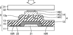
- FIG. 3 is a schematic diagram illustrating a cross section of the liquid crystal display panel of Embodiment 1.
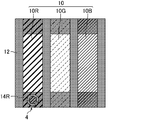
- FIG. 3 is a schematic diagram illustrating a display surface of the liquid crystal display panel of Embodiment 1.
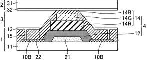
- 6 is a schematic cross-sectional view showing an application example 1 of the first embodiment.
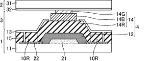
- FIG. 6 is a schematic cross-sectional view illustrating an application example 2 of the first embodiment.
- FIG. 6 is a schematic diagram showing a cross section of a liquid crystal display panel of Embodiment 2.
- FIG. 6 is a schematic diagram showing a cross section of a liquid crystal display panel of Embodiment 3.
- FIG. 6 is a schematic diagram showing a cross section of a liquid crystal display panel of Embodiment 4.
- FIG. 10 is a schematic diagram showing a cross section of a liquid crystal display panel of Embodiment 5.
- 7 is a schematic diagram illustrating a cross section of a liquid crystal display panel of Embodiment 6.
- FIG. It is a cross-sectional schematic diagram which shows a mode when external light reflects in the general liquid crystal display panel which uses an array board
- the integration of luminous reflection light intensity within the visible light wavelength range of the laminate in which the color materials of the transparent colored layer of Example 1 are stacked is different depending on the stacking order of the layers. It is a graph which shows the difference in a value. It is a graph which shows another example (Example 2) of the refractive index wavelength dispersion of each color material of the transparent coloring layer which comprises a lamination
- FIG. 10 is a schematic view showing a cross section of a liquid crystal display panel of Embodiment 7.
- FIG. 10 is a schematic diagram showing a display surface of a liquid crystal display panel of Embodiment 7. It is a schematic diagram which shows a cross section when the laminated spacer is used in the conventional liquid crystal display panel.
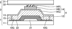
- FIG. 1 is a schematic view showing a cross section of the liquid crystal display panel of Embodiment 1.
- the liquid crystal display panel of Embodiment 1 has a structure in which a liquid crystal layer 3 is sandwiched between a pair of substrates 1 and 2, and controls the distance between the pair of substrates 1 and 2.
- a laminated spacer 4 is provided as a member. The laminated spacer 4 is formed on the array substrate 1.
- the liquid crystal display panel of Embodiment 1 can be applied to any mode such as the VA mode and the TN mode as long as the pair of substrates 1 and 2 have electrodes.
- the array substrate 1 includes a support substrate 11 made of glass, various wirings such as a gate wiring 21, a source wiring, and a drain wiring 22, TFTs connected to these wirings, and a plurality of sheets.
- a plurality of transparent colored layers 10R (outside the dotted line in FIG. 1) in the pixel opening region, and a laminated spacer 4 including a light shielding layer 12 and a plurality of colored transparent colored layers 14 laminated. ing.
- Various electrodes and wiring are isolated from each other through an interlayer insulating layer.
- the pixel electrode 13 is connected to the TFT via the drain wiring 22 and the contact hole 15 and is controlled individually.
- the counter substrate 2 includes a support substrate 31 and a common electrode 32.
- the laminated spacer 4 includes, from the support substrate 11 side, a light shielding layer 12, a red transparent colored layer (spacer red layer) 14R, a green transparent colored layer (spacer green layer) 14G, and blue A transparent colored layer (spacer blue layer) 14B is laminated in this order. As can be seen from the stacking order in FIG. 1, in the first embodiment, these layers are formed in the order of the light shielding layer 12, the red transparent colored layer 14R, the green transparent colored layer 14G, and the blue transparent colored layer 14B. .
- FIG. 2 is a schematic diagram illustrating a display surface of the liquid crystal display panel of the first embodiment.
- transparent colored layers 10R, 10G, and 10B of three colors of red, green, and blue are provided.
- the arrangement order is not particularly limited.
- the laminated spacer 4 is disposed in the red stripe region.
- the transparent colored layer is generally called a color filter, and can color display light by transmitting only a specific wavelength region of visible light.
- Color display is realized by arranging a plurality of transparent colored layers in combination.
- a region where the transparent colored layers 10R, 10G, and 10B are disposed is mainly used as a pixel opening region.
- the light shielding layer 12 is generally called a black matrix, and is disposed in a region where light shielding is necessary, such as a transparent colored interlayer region of different colors, a region where wiring, TFT, or the like is disposed. This region can also be formed by overlapping a plurality of transparent colored layers without providing the light shielding layer 12.
- each of the spacer red layer 14R, the spacer green layer 14G, and the spacer blue layer 14B constituting the laminated spacer is circular when the laminated spacer 4 is viewed from the normal direction, and each of these layers. Is cylindrical.
- the lower resin layer is formed wider than the region of the upper resin layer. By doing so, it is possible to secure a larger margin for the displacement of the layers in the stacking process.
- Each pixel electrode 13 is arranged at a certain interval in the pixel opening region.
- a red transparent colored layer 10R that overlaps the flat portion of the pixel electrode 13 is a red transparent colored layer (red display portion) 10R used as a pixel opening region, and overlaps a resin layer such as the light shielding layer 12.
- the red transparent colored layer 14 ⁇ / b> R is a red transparent colored layer (spacer red layer) 14 ⁇ / b> R used as the laminated spacer 4.
- the spacer red layer 14 ⁇ / b> R is integrally formed with the red transparent colored layer (red display portion) 10 ⁇ / b> R in the pixel opening region around the multilayer spacer 4.
- the spacer green layer 14G and the spacer blue layer 14B are separated from the green transparent coloring layer (green display portion) 10G in the pixel opening region and the blue transparent coloring layer (blue display portion) 10B in the pixel opening region. .
- another resin layer may be included in the laminated spacer 4.
- an alignment film may be formed so as to cover the entire laminated spacer 4.
- the alignment film can direct adjacent liquid crystal molecules in a desired direction by performing alignment treatment as necessary.
- the alignment process is mainly performed on the pixel opening region.
- the region adjacent to the laminated spacer 4 in the liquid crystal layer 3 is preferably not used as a pixel opening region because the alignment of the liquid crystal is affected by the laminated spacer 4. By providing the light shielding layer 12, it can be excluded from the pixel opening region.
- the uppermost layer among the transparent colored layers 14R, 14G, and 14B constituting the laminated spacer 4 so that the pixel electrode 13 of the array substrate 1 and the common electrode 32 of the counter substrate 2 are not in contact and short-circuited ( The pixel electrode 13 is not formed on the upper surface and the side surface of the spacer blue layer 14B) and the second layer from the top (spacer green layer 14G). On the other hand, the pixel electrode 13 is disposed on a part of the upper surface and the side surface of the third layer (spacer red layer 14R) located from the top.
- Each of the transparent colored layers 14R, 14G, and 14B constituting the laminated spacer 4 is formed such that the lower layer is wider than the upper layer.
- the method for forming the red transparent colored layers 14R and 10R, the green transparent colored layers 14G and 10G, the blue transparent colored layers 14B and 10B, and the light shielding layer 12 is not particularly limited.
- a liquid photosensitive resin (resist) material is applied to the film to form a photosensitive resin (resist) film, and the photosensitive resin (resist) film is patterned by photolithography, or a photosensitive resin on the substrate.
- a photosensitive resin film is transferred onto the support substrate 11 using a dry film provided with a film, and then the photosensitive resin film is patterned by photolithography.
- Examples of the material of the transparent colored layers 14R, 14G, 14B, 10R, 10G, 10B and the black matrix 12 include resin materials such as a photosensitive resin (resist).
- Examples of the material for the pixel electrode and the common electrode 13 include light-transmitting metal oxides such as indium tin oxide (ITO) and indium zinc oxide (IZO).
- a black matrix material a metal such as chromium may be used instead of a resin material.
- the black matrix is not a resin layer, so it is not considered as a constituent part of the laminated spacer in the present invention.
- FIG. 3 is a schematic cross-sectional view showing a state in which a liquid crystal display panel having a color filter-on-array configuration is pressed against a laminated spacer and a pixel electrode is cracked.
- the display surface of the liquid crystal display panel may be strongly pressed with an observer's finger or the like, and at this time, from the direction indicated by the arrow in FIG. When the pressure is applied, stress may be applied to the top of the laminated spacer 4.
- the hardness of the color material used for the transparent colored layer of the laminated spacer is the type, concentration, size, and dispersion state of the pigment component contained in the resin binder, and the presence or absence of a curing agent for stabilizing the shape. It depends on. When the pigment concentration is high or when a curing agent is included, the transparent colored layer becomes harder. When stress is applied to the top of the laminated spacer including a plurality of resin layers having different hardnesses, not all the layers are deformed in the same way, but the softer layers are more likely to be deformed. Further, the volume corresponding to the thickness reduced by the stress applied in the compression direction spreads in the panel in-plane direction perpendicular to the compression direction, and the deformation propagates to the peripheral portion of the spacer.
- An electrode is formed on the resin layer constituting the laminated spacer 4, but since the electrode cannot follow the deformation of the resin, a part of the highly transparent red transparent colored layer 14 ⁇ / b> R under the pixel electrode 13 is set. As shown in FIG. 3, the pixel electrode 13 may be cracked to form a crack portion 13a. Such cracks in the pixel electrode 13 are often formed in a substantially circular shape centering on the laminated spacer, and the range of the crack depends on the magnitude of the pressure from the outside. The crack of the pixel electrode 13 can cause a display defect because a correct electric field cannot be formed on the liquid crystal layer 3 in the adjacent region.
- the pixel electrode 13 on the array substrate 1 side has a common electrode 32 on the counter substrate 2 side.
- the pixel electrode is patterned in order to define the orientation direction when an electric field is applied, if the degree of damage to the pixel electrode 13 is large, the area of display failure when a disconnection occurs in the pixel electrode 13 May widen. Further, since this phenomenon is caused by the deformation of the red transparent colored layer 14R, it cannot be solved by removing the electrode on the red transparent colored layer 14R during patterning.
- the following measures are taken for such a problem.
- the deformation ratio of the red transparent colored layer 14R formed integrally with the display unit among the resin layers constituting the laminated spacer 4 is the deformation ratio of any other resin layer. It is formed to be smaller than that. As a result, the pixel electrode 13 is not easily cracked due to the deformation of the red transparent colored layer 14R, so that a liquid crystal display panel having good display characteristics without display defects can be obtained.
- the deformation amount ratio of the light shielding layer 12 located in the lower layer is the green transparent coloring layer 14G located in the upper layer. Is smaller than the deformation amount ratio of the blue transparent coloring layer 14B located in the upper layer, and the deformation amount ratio of the green transparent coloring layer 14G located in the lower layer is blue transparent located in the upper layer. It is formed to be smaller than the deformation amount ratio of the colored layer 14B. Such relative evaluation of the deformation amount ratio can be verified using an ultra-micro film hardness meter.
- the red transparent colored layer 14R is formed so that the hardness of the red transparent colored layer 14B is larger than the hardness of the green transparent colored layer 14G than the hardness of the green transparent colored layer 14G. . Thereby, the deformation amount ratio when stress is applied to the laminated spacer tends to be larger in the green transparent colored layer 14G or the blue transparent colored layer 14B.
- Examples of a method for adjusting the hardness of each layer constituting the laminated spacer 4 include a method of changing the ratio of the pigment in the solid content concentration of the color material. Specifically, as the pigment concentration in the solid content increases, a harder layer can be obtained. Moreover, the hardness of each layer can be adjusted also by adding a hardening
- the hardness adjustment of each layer constituting the laminated spacer 4 is not determined by an absolute value, but is determined by a relative relationship between the layers. This is because, as described above, it is preferable that the laminated spacer 4 has a certain deformation amount with respect to the stress, and it is important which layer has a larger deformation amount ratio in the entire deformation amount. is there. Therefore, in the first embodiment, the deformation amount ratio is concentrated on the light shielding layer 12, the green transparent colored layer 14G, and the blue transparent colored layer 14B that are not integrated with the transparent colored layer of the display unit.
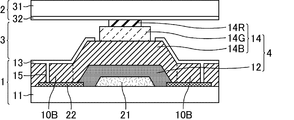
- the red transparent colored layer 14 ⁇ / b> R located at the bottom is shown integrated with the transparent colored layer of the display unit, but in Embodiment 1, for example, As shown in FIG. 4, the laminated spacer 4 is arranged in the green stripe region, and the green transparent colored layer 14G located in the middle of the three transparent colored layers of red, green and blue is integrated with the display unit.
- the deformation amount ratio of the green transparent coloring layer 14G is greater than the deformation amount ratio of the light-shielding layer 12, and the deformation amount ratio of the blue transparent coloring layer 14B. It is formed to be smaller than the deformation amount ratio (application example 1).
- FIG. 1 shows that the red transparent colored layer 14 ⁇ / b> R located at the bottom.
- the laminated spacer 4 is arranged in the blue stripe region, and the blue transparent colored layer 14 ⁇ / b> B located at the top among the three transparent colored layers of red, green, and blue is provided.
- the deformation ratio of the blue transparent coloring layer 14B may be greener than the deformation ratio of the red transparent coloring layer 14R than the deformation ratio of the light shielding layer 12.
- the transparent coloring layer 14G is formed so as to be smaller than the deformation amount ratio (Application Example 2).
- 4 is a schematic cross-sectional view showing an application example 1 of the first embodiment
- FIG. 5 is a schematic cross-sectional view showing an application example 2 of the first embodiment.
- FIG. 6 is a schematic view illustrating a cross section of the liquid crystal display panel of the second embodiment.
- the laminated spacer 4 is configured in such a manner that the black matrix 12, the spacer red layer 14R, the spacer blue layer 14B, and the spacer green layer 14G are laminated in this order from the support substrate 11 side.
- the rest is the same as in the first embodiment.
- the spacer red layer 14 ⁇ / b> R constituting the laminated spacer 4 is integrally formed with the red transparent colored layer (red display portion) 10 ⁇ / b> R. Therefore, the deformation amount ratio of the spacer red layer 14 ⁇ / b> R is formed to be smaller than the deformation amount ratio of the other resin layers constituting the laminated spacer 4.
- FIG. 7 is a schematic diagram illustrating a cross section of the liquid crystal display panel of the third embodiment.
- the laminated spacer 4 is configured in such a manner that the black matrix 12, the spacer green layer 14G, the spacer red layer 14R, and the spacer blue layer 14B are laminated in this order from the support substrate 11 side. However, the rest is the same as in the first embodiment.
- the spacer green layer 14G constituting the laminated spacer 4 is formed integrally with the green transparent colored layer (green display portion) 10G. Therefore, the deformation amount ratio of the spacer green layer 14 ⁇ / b> G is formed to be smaller than the deformation amount ratios of the other resin layers constituting the laminated spacer 4.
- FIG. 8 is a schematic diagram illustrating a cross section of the liquid crystal display panel of the fourth embodiment.
- the laminated spacer 4 is configured in such a manner that the black matrix 12, the spacer green layer 14G, the spacer blue layer 14B, and the spacer red layer 14R are laminated in this order from the support substrate 11 side. However, the rest is the same as in the first embodiment.
- the spacer green layer 14G constituting the laminated spacer 4 is formed integrally with the green transparent colored layer (green display portion) 10G. Therefore, the deformation amount ratio of the spacer green layer 14 ⁇ / b> G is formed to be smaller than the deformation amount ratios of the other resin layers constituting the laminated spacer 4.
- FIG. 9 is a schematic view showing a cross section of the liquid crystal display panel of the fifth embodiment.
- the laminated spacer 4 is configured in such a manner that the black matrix 12, the spacer blue layer 14B, the spacer red layer 14R, and the spacer green layer 14G are laminated in this order from the support substrate 11 side. However, the rest is the same as in the first embodiment.
- the spacer blue layer 14B constituting the laminated spacer 4 is formed integrally with the blue transparent colored layer (blue display portion) 10B. Therefore, the deformation amount ratio of the spacer blue layer 14 ⁇ / b> B is formed to be smaller than the deformation amount ratio of the other resin layers constituting the laminated spacer 4.
- FIG. 10 is a schematic diagram illustrating a cross section of the liquid crystal display panel of the sixth embodiment.
- the laminated spacer 4 is configured in such a manner that the black matrix 12, the spacer blue layer 14B, the spacer green layer 14G, and the spacer red layer 14R are laminated in this order from the support substrate 11 side. However, the rest is the same as in the first embodiment.
- the spacer blue layer 14B constituting the laminated spacer 4 is formed integrally with the blue transparent colored layer (blue display portion) 10B. Therefore, the deformation amount ratio of the spacer blue layer 14 ⁇ / b> B is formed to be smaller than the deformation amount ratio of the other resin layers constituting the laminated spacer 4.
- FIG. 11 is a schematic cross-sectional view showing a state in which external light is reflected in a general liquid crystal display panel that uses an array substrate and a color filter substrate separately.
- external light reflected by a general liquid crystal display panel that uses an array substrate 101 and a color filter substrate 102 separately is mostly reflected at the interface between air and a support substrate 131 (glass). is there.
- a support substrate 131 glass
- most of the light reflected at the interface between the red transparent colored layer 110R and the common electrode 132 is attenuated because it passes through the red transparent colored layer 110R twice.
- FIG. 12 is a schematic cross-sectional view showing a state when external light is reflected in a color filter on array liquid crystal display panel.
- the external light reflected by the color filter on-array liquid crystal display panel is not only the interface between air and the support substrate 31 (glass) but also between the color filter substrate 2 and the liquid crystal layer 3. Reflection also occurs at the interface and at the interface between the liquid crystal layer 3 and the array substrate 1. This is because the light reflected at these interfaces does not pass through the color filter and the reflected light is emitted to the outside without being attenuated. Such reflected light is visually recognized by an observer and adversely affects the display. For this, measures such as a method of reducing reflected light by utilizing the cell gap and the refractive index anisotropy of the liquid crystal material as described in Patent Document 4 are required.
- the interface between the resin layer that forms the top of the laminated spacer that forms the outermost surface of the array substrate and the alignment film that forms the outermost surface of the counter substrate cannot be solved by the above method.
- the generated reflected light is emitted to the outside as it is.
- the same color material of the laminated spacer is arranged at a constant period, the reflected light is strengthened by interference and is easily visually recognized.
- the spacer is disposed in a dark region such as on the wiring between pixels or on the light shielding layer, it is preferable that no reflected light is generated. If the display of the liquid crystal display panel is in the bright state, most of the light emitted from the liquid crystal display panel is in the pixel aperture region, so the reflection component of the external light is not noticeable. It stands out.
- a wavelength component having a reflectance that is easily visible to the human eye that is, a wavelength component having the highest luminous reflectance is 550 nm.
- a wavelength component having the highest luminous reflectance is 550 nm.
- the reflected light at these interfaces becomes strong, and materials with a refractive index closer to each other are arranged and laminated Compared with, the reflected light is more visible to human eyes. Therefore, as one of the methods for reducing the reflectance based on the structure of the laminated spacer, there is a method of paying attention to the change in the refractive index of the wavelength component at 550 nm and adjusting the change to the minimum.
- FIG. 13 is an enlarged schematic view of a region where the top of the laminated spacer of the array substrate is in contact with the surface of the counter substrate.
- light incident from the outside passes through the support substrate (glass) 31, the common electrode 32, and the alignment film 33 in order.
- the support substrate 31, the common electrode 32, and the alignment film 33 are all made of a light-transmitting material. Examples of the material of the alignment film 33 include polyimide and polyvinyl.
- the light that passes through the support substrate 31, the common electrode 32, and the alignment film 33 and reaches the interface between the alignment film 33 and the spacer blue layer 14 ⁇ / b> B that constitutes the uppermost layer of the stacked spacer 4 is aligned with the alignment film 33 and the spacer blue layer. It is separated into a component that reflects at the interface with 14B and a component that transmits through the spacer blue layer 14B.
- the component reflected at the interface between the alignment film 33 and the spacer blue layer 14B passes through the alignment film 33, the common electrode 32, and the support substrate 31 again and is emitted to the outside.
- the light that has passed through the spacer blue layer 14B reaches the interface between the spacer blue layer 14B and the spacer green layer 14G and is reflected at the interface between the spacer blue layer 14B and the spacer green layer 14G, and the spacer green layer 14G. It is separated into components that permeate through.
- the film thickness of each transparent coloring layer 14R, 14G, 14B constituting the laminated spacer 4 is determined by the pixel opening region. It becomes the same as the film thickness of the transparent colored layer. If it does so, the thickness of the transparent colored layer located on the uppermost will fully be ensured, and the intensity of the light when it permeate
- the relationship with the refractive index wavelength dispersion is most important. That is, the disturbance in the refractive index wavelength dispersion in the visible light wavelength region between the alignment film 33 and the spacer blue layer 14B is caused by the alignment film 33 and other transparent colored layers constituting the laminated spacer 4 (FIG. 13). Is smaller than the disturbance of the refractive index wavelength dispersion in the visible light wavelength region between the spacer red layer 14R and the spacer green layer 14G), so that the reflected light based on the structure of the laminated spacer 4 can be reduced. Occurrence can be further reduced.
- the thickness of the transparent colored layer is larger than the planar coated film thickness as going to the upper layer. May be thinner.
- the film thickness of the transparent coloring layer (spacer blue layer 14B in FIG. 13) located at the top is thin, before the intensity of light transmitted through the spacer blue layer 14B is sufficiently attenuated by the color material, The intensity of reflected light when reaching the interface with the transparent colored layer (spacer green layer 14G in FIG. 13) located second from the top increases. In that case, the refractive index wavelength dispersibility of the transparent colored layer (spacer blue layer 14B in FIG.
- refractive index wavelength dispersion of the spacer colored layer 14G) in FIG. 13 which is the second transparent colored layer from the top is important. That is, the disturbance of the refractive index wavelength dispersion in the visible light wavelength region between the spacer blue layer 14B and the spacer green layer 14G is caused by visible light between the spacer blue layer 14B and the spacer red layer 14R. It is preferable that the refractive index is less than the dispersion of the wavelength dispersion in the wavelength region, whereby the generation of reflected light based on the structure of the laminated spacer 4 can be further reduced.
- the refractive index wavelength dispersion of the coloring material within the visible light wavelength range can be measured using a refractive index measuring device such as an Abbe refractometer or a spectroscopic ellipsometer.
- the integral value of the luminous reflection light intensity within the visible light wavelength range of the color material can be measured using a spectral radiance meter.
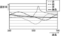
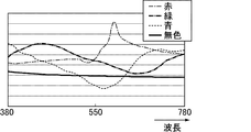
- FIG. 14 is a graph showing an example (Example 1) of the refractive index wavelength dispersion of each color material of the transparent colored layer constituting the laminated spacer and the refractive index wavelength dispersion of the colorless transparent layer (alignment film) material.
- the refractive index of the alignment film material at a wavelength of 550 nm is substantially the same as the refractive index of the green color material at a wavelength of 550 nm, and any of the red and blue transparent colored layers It is also different from the refractive index of the color material. Between the red transparent colored layer and the blue transparent colored layer, the refractive index difference between the red transparent colored layer and the color material of the blue transparent colored layer is smaller. Is larger.
- the refractive index of the color material of the green transparent colored layer at a wavelength of 550 nm is different from the refractive index of any of the color materials of the red and blue transparent colored layers at a wavelength of 550 nm.
- the refractive index difference with the color material of the transparent coloring layer is small, and the refractive index difference with the color material of the blue transparent coloring layer is larger.
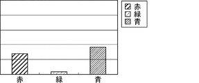
- FIG. 15 is a graph showing the integrated value of luminous reflection light intensity within the visible light wavelength range for each color material when the color material of each transparent coloring layer in Example 1 is superimposed on the alignment film material.
- the integral value of the luminous reflection light intensity in the visible light wavelength range of each color material at the alignment film interface is the smallest for green, greatly separated by red, and then by blue. Therefore, in Example 1, it is preferable that the transparent colored layer located on the top among the transparent colored layers constituting the laminated spacer is a green transparent colored layer.
- FIG. 16 shows the luminous reflection within the visible light wavelength range of each of the liquid crystal display panels of Embodiments 1 to 6 in the laminated body in which the color materials of the transparent colored layer of Example 1 are stacked, depending on the stacking order of the layers. It is a graph which shows the difference in the integrated value of light intensity.
- the integrated values of the luminous reflection light intensities in the visible light wavelength range of the respective laminates are the fifth embodiment, the second embodiment, the third embodiment, the first embodiment, the fourth embodiment, and the sixth embodiment. From the smallest to the largest. In particular, the difference between the fifth embodiment and the second embodiment and the difference between the second embodiment and each of the third, third, fourth, and sixth embodiments are large.
- the transparent colored layers constituting the laminated spacer are arranged in the order of green, red, and blue from the top.
- the order is most preferred, followed by the order of embodiment 2 in the order green, blue and red from the top.
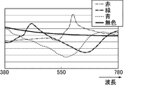
- FIG. 17 is a graph showing another example (Example 2) of the refractive index wavelength dispersion of each color material of the transparent colored layer constituting the laminated spacer and the refractive index wavelength dispersion of the colorless transparent layer (alignment film) material. It is. As shown in FIG. 17, in Example 2, the refractive index of the alignment film material at a wavelength of 550 nm is different from the refractive index of any color material of the red, green, and blue transparent coloring layers at a wavelength of 550 nm. The refractive index difference between the transparent coloring layer and the coloring material of the green transparent coloring layer is the smallest, and then the refractive index difference between the coloring material of the green transparent coloring layer and the coloring material of the red transparent coloring layer. The refractive index difference is the largest.
- the refractive index of the color material of the blue transparent coloring layer at a wavelength of 550 nm is different from the refractive index of any color material of the red and green transparent coloring layers at a wavelength of 550 nm.
- the refractive index difference between the red transparent coloring layer and the color material of the transparent colored layer is larger than the refractive index difference between the color material of the transparent colored layer and the transparent coloring layer.
- FIG. 18 is a graph showing the integrated value of luminous reflection light intensity within the visible light wavelength range for each color material when the color material of each transparent coloring layer in Example 2 is superimposed on the alignment film material.
- the integrated value of the luminous reflection light intensity in the visible light wavelength range of each color material at the alignment film interface is the smallest in blue, then green, and is far apart and large in red. Therefore, in Example 2, it is preferable that the transparent colored layer located on the top among the transparent colored layers constituting the laminated spacer is a blue transparent colored layer.
- FIG. 19 shows the luminous reflection within the visible light wavelength range of each of the liquid crystal display panels of Embodiments 1 to 6, in which the color layers of the transparent coloring layer of Example 2 are stacked, and the order of stacking the layers is different. It is a graph which shows the difference in the integrated value of light intensity.
- the integrated values of the luminous reflection light intensities in the visible light wavelength range of the respective laminates are the third embodiment, the first embodiment, the fifth embodiment, the second embodiment, the fourth embodiment, and the sixth embodiment. From the smallest to the largest. In particular, the difference between Embodiment 1 and Embodiment 5 and the difference between Embodiment 2 and Embodiments 4 and 6 are large.
- the transparent colored layers constituting the laminated spacer are arranged in the order of blue, red, and green from the top in the arrangement of Embodiment 3.
- the order is most preferred, followed by the order of embodiment 1, which is blue, green and red from the top.
- FIG. 20 is a graph showing another example (Example 3) of the refractive index wavelength dispersibility of each color material of the transparent colored layer constituting the laminated spacer and the refractive index wavelength dispersibility of the colorless transparent layer (alignment film) material. It is. As shown in FIG. 20, in Example 3, the refractive index of the alignment film material at a wavelength of 550 nm is different from the refractive index of any color material of the red, green, and blue transparent coloring layers at a wavelength of 550 nm. The refractive index difference between the transparent coloring layer and the coloring material of the green transparent coloring layer is the smallest, and then the refractive index difference between the coloring material of the green transparent coloring layer and the coloring material of the blue transparent coloring layer. The refractive index difference is the largest.
- the refractive index of the color material of the red transparent colored layer at a wavelength of 550 nm is different from the refractive index of any of the color materials of the green and blue transparent colored layers at a wavelength of 550 nm.
- the refractive index difference between the color material of the blue transparent coloring layer is larger than the refractive index difference between the color material of the transparent coloring layer.
- FIG. 21 is a graph showing the integrated value of luminous reflection light intensity within the visible light wavelength range for each color material when the color material of each transparent coloring layer in Example 3 is superimposed on the alignment film material.
- the integral value of the luminous reflection light intensity within the visible light wavelength range of each color material at the alignment film interface is the smallest for red, then green, and far away from it is blue. Therefore, in Example 3, it is preferable that the transparent colored layer located on the top among the transparent colored layers constituting the laminated spacer is a red transparent colored layer.
- FIG. 22 shows, for each of the liquid crystal display panels of Embodiments 1 to 6, luminous reflection within the visible light wavelength range due to the difference in the stacking order of the layers of the laminate in which the color materials of the transparent colored layer of Example 3 are stacked. It is a graph which shows the difference in the integrated value of light intensity.
- the integrated values of the luminous reflection light intensities in the visible light wavelength range of the respective laminates are the fourth embodiment, the sixth embodiment, the fifth embodiment, the second embodiment, the third embodiment, and the first embodiment. From the smallest to the largest. In particular, the difference between the second embodiment and each of the third and first embodiments is large.
- the transparent colored layers constituting the laminated spacer are arranged in the order of red, blue, and green from the top in the fourth embodiment.
- the order is preferred, followed by the order of embodiment 6 being red, green and blue from the top.
- the spectral luminous efficiency is taken into consideration from the refractive index wavelength dispersion characteristic of the material to be used so that the luminous reflectance to the human eye becomes smaller. It is preferable to determine the arrangement order of the transparent colored layers constituting the laminated spacer. That is, the integrated value of the luminous reflection light intensity in the visible light wavelength range of the laminate of the transparent colored layers of the plurality of colors is any of the laminates in the other arrangement order using the transparent colored layers of the same color. It is preferably smaller than the integrated value of the luminous reflection light intensity within the visible light wavelength range. Thereby, the reflected light can be reduced based on the structure of the laminated spacer.
- red (R) transparent colored layer the green (G) transparent colored layer
- blue (B) transparent colored layer the blue (B) transparent colored layer
- cyan ( C) transparent colored layer magenta (M) transparent colored layer
- yellow (Y) transparent colored layer etc. may be appropriately replaced with other colored transparent colored layers, and the arrangement order is determined in the same manner. Is preferred.
- FIG. 23 is a schematic view showing a cross section of the liquid crystal display panel of the seventh embodiment.
- the laminated spacer 4 includes the light shielding layer 12, the spacer yellow layer 14Y, the spacer red layer 14R, the spacer green layer 14G, and the spacer blue layer 14B in this order from the support substrate 11 side.
- FIG. 24 is a schematic diagram illustrating a display surface of the liquid crystal display panel of the seventh embodiment.
- four colored transparent layers 10R, 10G, 10B, and 10Y of red, green, blue, and yellow are provided in the seventh embodiment.
- the arrangement order is not particularly limited.
- the laminated spacer 4 is disposed in the yellow stripe region. Color reproducibility can be expanded by adding yellow to red, green and blue.
- the spacer yellow layer 14 ⁇ / b> Y is formed integrally with the yellow transparent colored layer (yellow display portion) 10 ⁇ / b> Y in the pixel opening region around the laminated spacer 4.
- the spacer red layer 14R, the spacer green layer 14G, and the spacer blue layer 14B are a red transparent colored layer (red display portion) 10R in the pixel opening region, a green transparent colored layer (green display portion) 10G in the pixel opening region, and It is separated from the blue transparent colored layer (blue display portion) 10B in the pixel opening region.
- the deformation ratio of the yellow transparent colored layer 14Y formed integrally with the display portion among the resin layers constituting the laminated spacer 4 is smaller than the deformation ratio of the other resin layers. It is formed to become. Further, the hardness of the yellow transparent colored layer 14Y is higher than the hardness of the red transparent colored layer 14R than the hardness of the light-shielding layer 12, and more than the hardness of the green transparent colored layer 14G. It is formed to be larger than the hardness.
- the deformation amount ratio when stress is applied to the laminated spacer is larger in the light shielding layer 12, the red transparent colored layer 14R, the green transparent colored layer 14G, or the blue transparent colored layer 14B, the yellow transparent Deformation hardly occurs in the colored layer 14Y, and the pixel electrode 13 is not easily cracked.
- the deformation amount ratio of the light shielding layer 12 is more green than the deformation amount ratio of the red transparent coloring layer 14R.
- the deformation amount ratio of the blue transparent coloring layer 14B is smaller than the deformation amount ratio of the blue transparent coloring layer 14B
- the deformation amount ratio of the red transparent coloring layer 14R is the deformation amount of the green transparent coloring layer 14G. It is formed so as to be smaller than the deformation amount ratio of the blue transparent coloring layer 14B, and the deformation amount ratio of the green transparent coloring layer 14G is smaller than the deformation amount ratio of the blue transparent coloring layer 14B. Is formed.
- Embodiments 8 to 30 In the liquid crystal display panels of Embodiments 8 to 30, in addition to the red (R) transparent coloring layer, the green (G) transparent coloring layer, and the blue (B) transparent coloring layer, yellow (Y) transparent coloring Four colors including layers are used. In the liquid crystal display panel of the seventh embodiment, these are laminated in the order of yellow, red, green and blue from the support substrate side, but in the eighth to thirtyth embodiments, the lamination order is different.
- Embodiment 8 Transparent colored layers are laminated in order of yellow, red, blue and green from the support substrate side.
- Embodiment 9 Transparent colored layers are laminated in order of yellow, green, red and blue from the support substrate side.
- Embodiment 10 Transparent colored layers are laminated in order of yellow, green, blue and red from the support substrate side
- Embodiment 11 Transparent colored layers are laminated in order of yellow, blue, red and green from the support substrate side
- Embodiment 12 Transparent colored layers are laminated in order of yellow, blue, green and red from the support substrate side
- Embodiment 13 Transparent colored layers in order of red, yellow, green and blue from the support substrate side
- Embodiment 14 Transparent colored layers are stacked in order of red, yellow, blue and green from the support substrate side
- Embodiment 15 Transparent in order of green, yellow, red and blue from the support substrate side Embodiment in which colored layer is laminated
- Embodiment 16 Green from support substrate side Embodiment 17 in which transparent colored layers are laminated in order of yellow, blue and red Embodiment 17: Embodiment in which transparent colored layers are laminated in order of blue, yellow, red and green Embodiment 18: from the side of the supporting substrate Embodiment 19
- the luminous reflectance to the human eye is It is preferable to determine the arrangement order of the transparent colored layers constituting the laminated spacer so as to be smaller. Thereby, the reflected light can be reduced based on the structure of the laminated spacer. That is, the integrated value of the luminous reflection light intensity in the visible light wavelength range of the laminate of the transparent colored layers of the plurality of colors is any of the laminates in the other arrangement order using the transparent colored layers of the same color. It is preferably smaller than the integrated value of the luminous reflection light intensity within the visible light wavelength range.
- the four colors of the transparent coloring layer of red (R), the transparent coloring layer of green (G), the blue (B), and the transparent coloring layer of yellow (Y) have been described. Similar to Embodiments 1 to 6, transparent colored layers of other colors may be used. Moreover, not only four colors but five or more colors may be used.
Landscapes
- Physics & Mathematics (AREA)
- Nonlinear Science (AREA)
- Mathematical Physics (AREA)
- Chemical & Material Sciences (AREA)
- Crystallography & Structural Chemistry (AREA)
- General Physics & Mathematics (AREA)
- Optics & Photonics (AREA)
- Liquid Crystal (AREA)
Abstract
本発明は、積層スペーサ上に絶縁層を設けなくとも、一対の基板間で電気的な短絡(リーク)が起こることを防止することができる液晶表示パネルを提供する。本発明の液晶表示パネルは、一対の基板と、上記一対の基板に挟持された液晶層とを有する液晶表示パネルであって、上記一対の基板の一方は、支持基板と、複数の画素電極と、上記複数の画素電極と重畳する複数色の透明着色層と、複数色の透明着色層を含む3以上の樹脂層を積層して含む積層スペーサとを有し、上記一対の基板の他方は、支持基板と、共通電極とを有する液晶表示パネルである。
Description
本発明は、液晶表示パネルに関する。より詳しくは、カラーフィルタの積層体をスペーサとして用いる液晶表示パネルに関する。
液晶表示(LCD:Liquid Crystal Display)装置は、一対の基板間に液晶層を挟持した構成を有し、基板に形成した電極により液晶層に電圧を印加して液晶分子の配向状態を変化させ、液晶層を透過する光の偏光状態を変化させて表示を行う。
液晶層を挟持する一対の基板は、スペーサによってその間隔(セルギャップ)が一定に保持され、シール材によって互いが貼り合わされている。スペーサとしては、例えば、透明のビーズ状のものが挙げられるが、散布されたスペーサが不均一になるとコントラストが低下するおそれがあることから、柱状のスペーサが用いられることもある(例えば、特許文献1~6参照。)。
柱状のスペーサについては、製造工程を簡略化するために、画素開口領域において赤、緑及び青等の複数色のカラーフィルタを形成すると同時に、ブラックマトリクス上の所定の複数箇所に各色のカラーフィルタを形成して、赤、緑及び青の3色のカラーフィルタが積み上げられた凸部を形成し、この凸部を柱状スペーサとして用いることもある(例えば、特許文献7~9参照。)。
一般的には、液晶層を挟持する一対の基板は、液晶層に電圧を印加するための電極、配線、TFT(Thin Film Transistor)等のスイッチング素子を有するアレイ基板と、カラー表示を行うためのカラーフィルタ、ブラックマトリクス等を有するカラーフィルタ基板とのそれぞれ別個の基板で構成される。
一方で、近年、カラーフィルタ、ブラックマトリクス等の部材をアレイ基板側に形成する、いわゆるカラーフィルタ(CF)オンアレイが検討されている。CFオンアレイによれば、一対の基板のそれぞれに形成される各部材の位置あわせマージンを考慮する必要がなく、製造工程が簡略化できると同時に、画素開口率の拡大も達成される(例えば、特許文献10参照。)。
図25は、従来の液晶表示パネルにおいて、カラーフィルタやブラックマトリクス等を積層して形成した柱状スペーサ(以下、積層スペーサともいう。)を用いたときの断面を示す模式図である。図25で示される液晶表示パネルは、アレイ基板101と、カラーフィルタ基板102と、これらの間に配置された液晶層103とを有している。
アレイ基板101は、ガラス等でできた支持基板111上に、ゲート配線121、ソース配線、ドレイン配線122等の各種配線、及び、これらの配線と接続されたTFTを有しており、これらは層間絶縁層116を介してそれぞれ隔離されている。層間絶縁層116上には画素電極113が複数枚配置されており、画素電極113はそれぞれ、層間絶縁層116内に設けられたコンタクトホール115を介して、所定の信号を供給するドレイン配線122と接続されている。これにより、個別に画素電極113に電荷が充電される。
カラーフィルタ基板102は、各画素電極113と液晶層103を介して対向する各色のカラーフィルタを有しており、各カラーフィルタの間隙にブラックマトリクス(BM)を有している。積層スペーサ104は、カラーフィルタ基板102側の支持基板131上に設けられており、支持基板131側から、ブラックマトリクス112、赤(R)のカラーフィルタ114R、緑(G)のカラーフィルタ114G、及び、青(B)のカラーフィルタ114Bの順にこれらが積層されて構成されている。また、積層スペーサ104の表面全体を共通電極132が覆っており、共通電極132上にはキャップ絶縁層117が設けられている。すなわち、カラーフィルタ基板102は、液晶層103に向かって、支持基板131、積層スペーサ104、共通電極132、及び、キャップ絶縁層117をこの順に積層して有している。積層スペーサ104の表面全体を覆う共通電極132は、画素開口領域においてカラーフィルタ上に形成される共通電極と同時に形成される。共通電極132上に形成されたキャップ絶縁層117は、カラーフィルタ基板102の共通電極132とアレイ基板101の画素電極113とが導通することを防ぐために形成される絶縁層である。一対の基板のそれぞれに設けられた電極間に一定間隔が空けられたとしても、一対の基板の貼り合わせズレによりそれぞれが短絡(リーク)を起こすと、画素欠陥が生じ、表示不良を引き起こす可能性がある。
本発明者らは、液晶層を挟持する一対の基板の間隔を保持するスペーサとして、カラーフィルタやブラックマトリクス等を積層した積層スペーサを利用する場合について種々検討を行っていたところ、従来の積層スペーサでは、上述のように、共通電極上にキャップ絶縁層を形成することで導通を予防することは可能であるが、キャップ絶縁層の塗布工程及びパターニング工程等の余分な製造工程が必要となってしまう点に着目した。また、積層スペーサがアレイ基板と接触する領域において画素電極の一部が除去されるようにパターニングすることで導通を防ぐことも考えられるが、一対の基板の貼りあわせ時に生じるズレを考慮しておく必要があり、かつ積層スペーサがアレイ基板と接触する面積よりも大きな面積の電極を除去しなければならないため、画素開口領域の開口面積にロスが生じうる点に着目した。
本発明は、上記現状に鑑みてなされたものであり、積層スペーサを用いる場合に、製造工程を余分に増やさなくとも、一対の基板間で電気的な短絡(リーク)が起こることを防止することができる液晶表示パネルを提供することを目的とするものである。
本発明者らは、従来においては、積層スペーサがカラーフィルタ基板側に設けられており、製造工程上、積層スペーサの全体が共通電極で覆われる必要があった点に着目した。そして、積層スペーサをアレイ基板側に設ければ、アレイ基板においては画素電極がパターニングされる必要があるため、工程数を増やさなくとも積層スペーサの全体に画素電極を形成する必要がなく、アレイ基板側に積層スペーサを設けることで、一対の基板のそれぞれに設けられた電極同士が短絡(リーク)を起こすことを防止することができることを見いだし、上記課題をみごとに解決することができることに想到し、本発明に到達したものである。
すなわち、本発明は、一対の基板と、上記一対の基板に挟持された液晶層とを有する液晶表示パネルであって、上記一対の基板の一方は、支持基板と、複数の画素電極と、上記複数の画素電極と重畳する複数色の透明着色層と、複数色の透明着色層を含む3以上の樹脂層を積層して含む積層スペーサとを有し、上記一対の基板の他方は、支持基板と、共通電極とを有する液晶表示パネルである。
本発明の液晶表示パネルについて、以下に詳しく説明する。
本発明の液晶表示パネルは、一対の基板と、上記一対の基板に挟持された液晶層とを有する。一対の基板の一方又は両方に、電極、配線、スイッチング素子等の部材を設けて液晶層内の液晶分子の配向性を制御することで、液晶層を透過する光の偏光状態を変化させ、所望の画像表示を得ることができる。
上記一対の基板の一方(以下、アレイ基板ともいう。)は、支持基板と、複数の画素電極と、上記複数の画素電極と重畳する複数色の透明着色層と、複数色の透明着色層を含む3以上の樹脂層を積層して含む積層スペーサとを有する。画素電極を透明着色層と対応させて配置することで、透明着色層単位で液晶の配向を制御することができる。このように画素電極が配置された領域は画素開口領域となり、複数色の透明着色層のカラーバランスを調節することで、様々な表示色を表現することができる。
本発明の液晶表示パネルは、いわゆるカラーフィルタオンアレイの一形態であり、アレイ基板に、複数色の透明着色層と、複数の画素電極との両方が設けられている。カラーフィルタオンアレイの構造とすることで、透明着色層と画素電極とを別々の基板に設けたときと比べ、位置あわせマージンを大きく取ることができ、製造工程が簡略化され、かつ画素開口率も拡大する。
また、本発明の液晶表示パネルにおいては、透明着色層及び画素電極が形成された基板と同じ基板に、積層スペーサが設けられている。積層スペーサを構成する各層は、画素開口領域に形成される透明着色層に使用される材料と同じ材料を用いることができ、画素開口領域における透明着色層と一体化されていても、別々に配置されていてもよい。また、積層スペーサを構成する樹脂層の種類は特に限定されず、画素開口領域で用いられる透明着色層、遮光層のほか、必要に応じて他の樹脂層を重ね合わせてもよい。
上記画素電極は、複数が個別に配置されるので、製造工程においてパターニングの必要がある。したがって、画素電極の製造工程において積層スペーサが形成された領域を除外するパターニングを行うことで、積層スペーサの表面に導電部材が形成されることもなくなるため、上記一方の基板の他方の基板との間でのリークを防ぐことができる。すなわち、上記画素電極は、上記積層スペーサを構成する樹脂層の最上層を覆っていないことが好ましく、上記画素電極は、上記積層スペーサを構成する樹脂層の上から2番目に位置する樹脂層を覆っていないことが好ましく、上記積層スペーサを構成する樹脂層の上から3番目に位置する樹脂層を覆っていないことが好ましい。
上記一対の基板の他方(以下、対向基板ともいう。)は、支持基板と、共通電極とを有する。すなわち、本発明の液晶表示パネルは、液晶層を挟持する一対の電極を有している。これにより、液晶層内に容易に電界を形成することができ、液晶分子の配向性を印加電圧の大きさによって調節することができる。
本発明の液晶表示パネルの構成としては、このような構成要素を必須として形成されるものである限り、その他の構成要素により特に限定されるものではない。
以下に、本発明の液晶表示パネルの好ましい形態について詳述する。
上記複数の画素電極と重畳する複数色の透明着色層の少なくとも一つは、上記積層スペーサに含まれる同色の透明着色層と一体化されていることが好ましい。積層スペーサを構成する層のうちの一つを画素開口領域の透明着色層と一体化することにより、積層時の重ねマージンを大きくすることができる。
上記一体化された透明着色層の変形量割合は、上記積層スペーサに含まれる他の樹脂層の変形量割合よりも小さいことが好ましい。本明細書において「変形量割合」とは、積層スペーサ全体の変形量に対する各樹脂層の変形量の割合をいう。積層スペーサを構成する複数色の透明着色層のうち、画素開口領域の透明着色層と一体化されているものは、積層スペーサに対して応力がかかったときの変動の影響により、画素電極に割れ(クラック)を生じさせやすい。そこで、積層スペーサを構成する複数色の透明着色層のうち、画素開口領域の透明着色層と一体化されている透明着色層の変形量割合を最も小さくすることで、画素電極に断絶が起こる可能性を低減し、画素欠陥の発生を防ぐことができる。
変形量の調節を行う一例としては、各樹脂層の硬さを調節する方法が挙げられる。樹脂層の硬さをより硬く形成することで、より変形量は小さくなり、樹脂層の硬さをより軟らかく形成することで、より変形量は大きくなる傾向にある。したがって、上記一体化された透明着色層は、上記積層スペーサに含まれる他の樹脂層よりも硬いことが好ましい。これにより、積層スペーサに対し応力がかかったときの各樹脂層の変形を、より他の樹脂層に集中させやすくなる。
上記一体化された透明着色層以外の樹脂層の変形量割合は、より上層に位置する樹脂層よりも、より下層に位置する樹脂層で小さいことが好ましい。これにより、より下層の樹脂層上に形成される画素電極に割れ(クラック)が起こりにくくなる。また、同様に、上記一体化された透明着色層以外の樹脂層の硬さは、より上層に位置する樹脂層よりも、より下層に位置する樹脂層で硬いことが好ましい。より硬い樹脂層を積層スペーサの下層に配置し、よりやわらかい樹脂層を積層スペーサの上層に配置することで、積層スペーサに対し応力がかかったときの各樹脂層の変形を、より上層に集中させやすくなる。
上記複数色の透明着色層のうちで最も上に位置する透明着色層の上に位置する層は、無色透明層であることが好ましい。カラーフィルタオンアレイの液晶表示パネルでは、カラーフィルタが配置された基板と対向する基板には、通常、ガラス、プラスチック等の透明基板、透明電極、配向膜等の透光性を有する部材が用いられる。また、カラーフィルタが配置された基板において、画素開口領域内に形成される配向膜を、積層スペーサ上の全体にも形成することで、余分なパターニング工程を行わなくて済む。そのため、積層スペーサの透明着色層の上層は、このような無色透明層で構成されることが生産性の観点から好ましい。
上記無色透明層の波長550nmにおける光の屈折率と、上記最も上に位置する透明着色層の波長550nmにおける光の屈折率との間の差は、上記無色透明層の波長550nmにおける光の屈折率と、上記複数色の透明着色層のうちで上から2番目に位置する透明着色層の波長550nmにおける光の屈折率との差よりも、小さいことが好ましい。カラーフィルタオンアレイの液晶表示パネルでは、アレイ基板とカラーフィルタ基板とが別々に用いられる液晶表示パネルと異なり、積層スペーサを構成する透明着色層の最表面における反射が問題となりうる。そのため、屈折率界面での反射を減らすために、特に人間の目が視認しやすい550nmにおいて透明着色層上に配置される無色透明層との間での視感度反射率が低い透明着色層をより上層に配置することで、透明着色層上に配置される無色透明層と透明着色層との間で生じる光の視感反射光強度の大きさを小さくすることができ、積層スペーサが有する透明着色層の構造に基づく反射を効果的に低減することができる。
上記複数色の透明着色層の積層体の可視光波長範囲内における視感反射光強度の積分値は、同色の透明着色層を用いて他の配置順としたときのいずれの積層体の可視光波長範囲内における視感反射光強度の積分値よりも、小さいことが好ましい。
人間の目は、可視光の波長範囲(380nm~780nm)内における反射光強度の大きさに基づき、反射光を感知する。人間の目が感知するトータルの視感反射光強度は、具体的には、波長分散特性をもつ各波長成分の反射光強度に対して、CIE(国際照明委員会)が規定している分光視感効率を掛け合わせて得られる値を、可視光波長範囲内で積分させることによって、算出することができる。カラーフィルタオンアレイの液晶表示パネルでは、アレイ基板とカラーフィルタ基板とが別々に用いられる液晶表示パネルと異なり、積層スペーサを構成する透明着色層に基づく反射が問題となりうる。積層スペーサを構成する透明着色層に入射した光は、透明着色層を通過する際に減衰するため、積層スペーサの構造に基づく光の反射は、最も上に位置する透明着色層と、その上層との界面での反射が最も影響が大きい。ただし一方で、透明樹脂層を複数積み重ねて形成される積層スペーサでは、最も上に位置する透明着色層と、上から2番目に位置する透明着色層との間で生じる反射の影響も受ける。この影響は、特に最も上に位置する透明着色層の厚みが薄く形成される場合に大きく、この場合、積層スペーサを構成する透明着色層に入射した光が透明着色層を通過する際に充分に減衰されないためである。このことから、積層スペーサを構成する透明着色層の積層順を決定するに当たっては、複数の透明着色層の積層順の組み合わせのうち、最も反射率が低い組み合わせの積層体を選ぶことが好ましい。
本発明の液晶表示パネルによれば、積層スペーサを用いたとしても、一対の基板のそれぞれに設けられた電極同士が短絡することを防ぐことができ、かつアレイ基板とカラーフィルタ基板とが別々の基板で用いられることによる貼り合わせズレの問題を解消することができる。
以下に実施形態を掲げ、本発明について図面を参照して更に詳細に説明するが、本発明はこれらの実施形態のみに限定されるものではない。
実施形態1
図1は、実施形態1の液晶表示パネルの断面を示す模式図である。図1に示すように、実施形態1の液晶表示パネルは、一対の基板1,2間に液晶層3が挟持された構造を有しており、一対の基板1,2間の間隔を制御する部材として、積層スペーサ4が設けられている。積層スペーサ4は、アレイ基板1に形成されている。
図1は、実施形態1の液晶表示パネルの断面を示す模式図である。図1に示すように、実施形態1の液晶表示パネルは、一対の基板1,2間に液晶層3が挟持された構造を有しており、一対の基板1,2間の間隔を制御する部材として、積層スペーサ4が設けられている。積層スペーサ4は、アレイ基板1に形成されている。
実施形態1の液晶表示パネルは、一対の基板1,2がそれぞれ電極を有する限り、VAモード、TNモード等のいずれのモードにも適用することができる。
図1に示すように、アレイ基板1は、ガラス等でできた支持基板11と、ゲート配線21、ソース配線、ドレイン配線22等の各種配線と、これらの配線と接続されたTFTと、複数枚の画素電極13と、画素開口領域における複数色の透明着色層10R(図1における点線から外側)と、遮光層12及び複数色の透明着色層14を積層して含む積層スペーサ4とを有している。各種電極及び配線は、層間絶縁層を介してそれぞれ隔離されている。画素電極13は、ドレイン配線22及びコンタクトホール15を介してTFTとそれぞれ接続されており、それぞれが個別に制御される。実施形態1において対向基板2は、支持基板31と共通電極32とを有している。
図1に示すように、積層スペーサ4は、支持基板11側から、遮光層12、赤色の透明着色層(スペーサ赤層)14R、緑色の透明着色層(スペーサ緑層)14G、及び、青色の透明着色層(スペーサ青層)14Bの順にこれらが積層された構成を有する。図1における積層順から分かるように、実施形態1では、遮光層12、赤色の透明着色層14R、緑色の透明着色層14G、及び、青色の透明着色層14Bの順にこれらの層が形成される。
図2は、実施形態1の液晶表示パネルの表示面を示す模式図である。図2に示すように、実施形態1では、赤、緑及び青の3色の透明着色層10R,10G,10Bが設けられている。配置順は特に限定されない。積層スペーサ4は、赤のストライプ領域内に配置されている。透明着色層は、一般にカラーフィルタとも呼ばれ、可視光のうち特定の波長域のみを透過させることにより表示光の着色を行うことができる。複数色の透明着色層を組み合わせて配置することでカラー表示が実現される。透明着色層10R,10G,10Bが配置される領域が、主に画素開口領域として利用される。
遮光層12は、一般にブラックマトリクスとも呼ばれ、異なる色の透明着色層間領域、配線、TFT等が配置された領域等、遮光が必要な領域に配置される。この領域は、遮光層12を設けることなく、複数色の透明着色層を重ね合わせることによっても形成可能である。
図2に示すように、積層スペーサを構成するスペーサ赤層14R、スペーサ緑層14G及びスペーサ青層14Bのそれぞれは、積層スペーサ4を法線方向からみたときに円形であり、かつ、これらの各層は円柱状である。また、これらの各層は、より下に位置する樹脂層が、より上に位置する樹脂層の領域よりも広く形成されている。こうすることで、積層プロセスでの層の配置ずれに対するマージンを、より多く確保することができる。
各画素電極13は、画素開口領域において一定の間隔を空けて配置される。画素電極13の平坦な部分と重なっている赤の透明着色層10Rが、画素開口領域として用いられる赤の透明着色層(赤表示部)10Rであり、遮光層12等の樹脂層と重なっている赤の透明着色層14Rが、積層スペーサ4として用いられる赤の透明着色層(スペーサ赤層)14Rである。
スペーサ赤層14Rは、積層スペーサ4の周囲の画素開口領域の赤色の透明着色層(赤表示部)10Rと一体的に形成されている。スペーサ緑層14G及びスペーサ青層14Bは、画素開口領域の緑色の透明着色層(緑表示部)10G、及び、画素開口領域の青色の透明着色層(青表示部)10Bとは分離されている。
スペーサとしての高さが不充分な場合には、他の樹脂層を積層スペーサ4に含めてもよい。また、積層スペーサ4の全体を覆うようにして配向膜が形成されていてもよい。配向膜は、必要に応じて配向処理を行うことで、隣接する液晶分子を所望の方向に向けることができる。配向処理は、主に画素開口領域に対して行われる。
液晶層3のうち積層スペーサ4に隣接する領域は、積層スペーサ4によって液晶の配向が影響を受けるので画素開口領域としては利用されないことが好ましい。遮光層12を設けることにより、画素開口領域から除外することができる。
アレイ基板1の画素電極13と、対向基板2の共通電極32とが接触して短絡しないように、積層スペーサ4を構成する透明着色層14R,14G,14Bのうち、最も上に位置する層(スペーサ青層14B)、並びに、上から2番目に位置する層(スペーサ緑層14G)の上面及び側面には、画素電極13が形成されていない。一方、上から3番目に位置する層(スペーサ赤層14R)の上面及び側面の一部には画素電極13が配置されている。積層スペーサ4を構成する各透明着色層14R,14G,14Bは、いずれもが、より下層の幅がより上層の幅よりも広くなるように形成されている。
赤色の透明着色層14R,10R、緑色の透明着色層14G,10G、青色の透明着色層14B,10B、及び、遮光層12の形成方法としては特に限定されず、例えば、コーターにより支持基板11上に液状の感光性樹脂(レジスト)材料を塗布して感光性樹脂(レジスト)膜を成膜し、更にフォトリソグラフィにより感光性樹脂(レジスト)膜をパターニングする方法や、基材上に感光性樹脂膜が設けられたドライフィルムを用いて支持基板11上に感光性樹脂膜を転写し、更にフォトリソグラフィにより感光性樹脂膜をパターニングする方法が挙げられる。
透明着色層14R,14G,14B,10R,10G,10B、及び、ブラックマトリクス12の材料としては、感光性樹脂(レジスト)等の樹脂材料が挙げられる。画素電極、及び、共通電極13の材料としては、酸化インジウム錫(ITO)、酸化インジウム亜鉛(IZO)等の透光性を有する金属酸化物が挙げられる。なお、ブラックマトリクスの材料として、樹脂材料ではなくクロム等の金属を用いてもよいが、この場合のブラックマトリクスは樹脂層ではないので、本発明における積層スペーサの構成部位とは考えない。
ここで、液晶表示パネルを構成する一対の基板に対し押圧がかかったときの課題について説明する。
図3は、カラーフィルタオンアレイの形態を有する液晶表示パネルにおいて、積層スペーサに対し押圧がかかり画素電極にひび割れが生じたときの状態を示す断面模式図である。特に、携帯機器の表示装置、タッチパネルを備える表示装置では、液晶表示パネルの表示面が観察者の指等で強く押されることがあり、このとき、図3の矢印で示す方向(外界側)から押圧がかかることで積層スペーサ4の頂部に応力がかかることがある。
対向基板2側の支持基板31に対して一定以上の押圧がかかると、積層スペーサの頂上に対して応力印加がかかり、積層スペーサ4を構成する各樹脂層にその力が伝播して各樹脂層に変形が起こる。一般的に、一対の基板を貼り合わせて形成される液晶表示パネルにおいて基板間隔を保持するスペーサは、液晶層の体積変動に対応できる柔軟性が求められる。スペーサが硬すぎると、液晶層の体積減少による気泡の発生や、液晶層の体積増加によってスペーサが対向基板から離れ、局所的なムラを生じやすい。そのため、スペーサは外界からの応力に対して変形可能であることが好ましい。
硬質なガラスや金属材料ではなく、軟質な樹脂材料をスペーサの材料に用いることで、外部の応力に対して変形可能なスペーサを得ることができる。ただし、積層スペーサの透明着色層に用いられる色材の硬度は、樹脂バインダーに含まれる顔料成分の種類、濃度、大きさ、及び、分散状態、並びに、形状を安定化させるための硬化剤の有無によって異なる。顔料濃度が高い場合や硬化剤が含まれる場合には、透明着色層はより硬くなる。硬さの異なる複数の樹脂層を含む積層スペーサの頂上に応力を印加すると、全ての層が同じように変形をするのではなく、柔らかい層ほど変形が起こりやすい。また、圧縮方向に加えられた応力により減少した厚さ分の体積は、圧縮方向に垂直なパネル面内方向に広がり、スペーサの周辺部にまで変形が伝播する。
積層スペーサ4を構成する樹脂層上には電極が形成されるが、電極は樹脂の変形に追随することができないため、画素電極13下の変形の大きな赤の透明着色層14Rの一部がせり上がり、図3に示すように、画素電極13に割れが生じてクラック部13aが生じることがある。このような画素電極13の割れは、積層スペーサを中心とした略円状に形成されることが多く、割れの範囲は、外界からの押圧の大きさに依存する。画素電極13の割れは、隣接領域の液晶層3に対して正しい電界を形成できないために表示不良の原因となりうるが、特にアレイ基板1側の画素電極13は、対向基板2側の共通電極32と異なり電界印加時の配向方向を規定するために画素電極がパターニングされている場合があり、画素電極13の損傷の程度が大きいと、画素電極13内に断線が起こったときの表示不良の面積が広くなるおそれがある。また、この現象は、赤の透明着色層14Rの変形に起因しているため、赤の透明着色層14R上の電極をパターニングの際に除外することによって解決するものでもない。
これは、画素電極とカラーフィルタとが同一基板内に形成されるカラーフィルタオンアレイ特有の課題であり、画素の境界に関わらずカラーフィルタ基板の全体に共通電極が形成される一般的な液晶表示パネルでは、ここまでの大きな影響は生じない。
実施形態1の液晶表示パネルでは、このような課題に対し、以下の工夫を行っている。
実施形態1においては、積層スペーサ4を構成する各樹脂層のうち、表示部と一体化されて形成される赤の透明着色層14Rの変形量割合が、他のいずれの樹脂層の変形量割合よりも小さくなるように形成されている。これにより、赤の透明着色層14Rの変形に起因した画素電極13の割れが起こりにくくなるため、表示不良のない良好な表示特性をもつ液晶表示パネルを得ることができる。
なお、赤の透明着色層14Rを除く、他の樹脂層間の変形量割合の相関関係については、より下層に位置する遮光層12の変形量割合が、より上層に位置する緑の透明着色層14Gの変形量割合よりも、上層に位置する青の透明着色層14Bの変形量割合よりも小さく、より下層に位置する緑の透明着色層14Gの変形量割合が、より上層に位置する青の透明着色層14Bの変形量割合よりも小さくなるように形成されている。このような変形量割合の相対評価は、超微小膜硬度計を用いて検証することができる。
また、赤の透明着色層14Rの硬さが、遮光層12の硬さよりも、緑の透明着色層14Gの硬さよりも、青の透明着色層14Bの硬さよりも大きくなるように形成されている。これにより、積層スペーサに応力がかかったときの変形量割合が、緑の透明着色層14G又は青の透明着色層14Bにおいてより大きくなりやすい。
積層スペーサ4を構成する各層の硬さを調節する方法としては、例えば、色材の固形分濃度における顔料の比率を変化させる方法が挙げられる。具体的には、固形分中の顔料濃度が上がれば上がるほど、より硬い層を得ることができる。また、固形分中に硬化剤を加えることによっても、各層の硬さを調節することができる。更に、透明着色層を形成する際の、焼成条件、露光条件、及び、現像条件によっても、各層の硬さは調節可能である。なお、このような硬さの相対評価は、表示部と一体化される透明着色層がそれぞれ異なる複数のサンプルを用意し、各サンプルに対して同じ応力を加える試験を行い、それぞれの割れの程度を比較することで検証することができる。
実施形態1において積層スペーサ4を構成する各層の硬さ調整は、絶対的な値で決まるものではなく、各層の相対関係で決定される。これは、上述したように、積層スペーサ4が応力に対して一定の変形量をもつことが好ましく、全体の変形量の中でどの層がより大きな変形量割合をもつかが重要となるためである。したがって、実施形態1では、表示部の透明着色層と一体化されていない遮光層12、緑の透明着色層14G、及び、青の透明着色層14Bに変形量割合を集中させている。
図1においては、複数の透明着色層のうち、最も下に位置する赤の透明着色層14Rが表示部の透明着色層と一体化した形態を示しているが、実施形態1においては、例えば、図4に示すように、積層スペーサ4を緑のストライプ領域に配置し、赤、緑及び青の3つの透明着色層のうち、真ん中に位置する緑の透明着色層14Gが表示部と一体化してもよく、この場合には、緑の透明着色層14Gの変形量割合が、遮光層12の変形量割合よりも、赤の透明着色層14Rの変形量割合よりも、青の透明着色層14Bの変形量割合よりも小さくなるように形成されている(応用例1)。そして、同様に、図5に示すように、積層スペーサ4を青のストライプ領域に配置し、赤、緑及び青の3つの透明着色層のうち、最も上に位置する青の透明着色層14Bが表示部と一体化してもよく、この場合には、青の透明着色層14Bの変形量割合が、遮光層12の変形量割合よりも、赤の透明着色層14Rの変形量割合よりも、緑の透明着色層14Gの変形量割合よりも小さくなるように形成されている(応用例2)。図4は、実施形態1の応用例1を示す断面模式図であり、図5は、実施形態1の応用例2を示す断面模式図である。
以下に、本発明の他の実施形態ついて詳述する。
実施形態2
図6は、実施形態2の液晶表示パネルの断面を示す模式図である。実施形態2において積層スペーサ4は、支持基板11側から、ブラックマトリクス12、スペーサ赤層14R、スペーサ青層14B、及び、スペーサ緑層14Gの順にこれらが積層されて構成されている点で実施形態1と相違しているが、それ以外は実施形態1と同様である。実施形態2では、積層スペーサ4を構成するスペーサ赤層14Rが、赤色の透明着色層(赤表示部)10Rと一体的に形成されている。そのため、スペーサ赤層14Rの変形量割合が、積層スペーサ4を構成する他の樹脂層の変形量割合よりも小さくなるように形成されている。
図6は、実施形態2の液晶表示パネルの断面を示す模式図である。実施形態2において積層スペーサ4は、支持基板11側から、ブラックマトリクス12、スペーサ赤層14R、スペーサ青層14B、及び、スペーサ緑層14Gの順にこれらが積層されて構成されている点で実施形態1と相違しているが、それ以外は実施形態1と同様である。実施形態2では、積層スペーサ4を構成するスペーサ赤層14Rが、赤色の透明着色層(赤表示部)10Rと一体的に形成されている。そのため、スペーサ赤層14Rの変形量割合が、積層スペーサ4を構成する他の樹脂層の変形量割合よりも小さくなるように形成されている。
実施形態3
図7は、実施形態3の液晶表示パネルの断面を示す模式図である。実施形態3において積層スペーサ4は、支持基板11側から、ブラックマトリクス12、スペーサ緑層14G、スペーサ赤層14R、及び、スペーサ青層14Bの順にこれらが積層されて構成されている点で実施形態1と相違しているが、それ以外は実施形態1と同様である。実施形態3では、積層スペーサ4を構成するスペーサ緑層14Gが、緑色の透明着色層(緑表示部)10Gと一体的に形成されている。そのため、スペーサ緑層14Gの変形量割合が、積層スペーサ4を構成する他の樹脂層の変形量割合よりも小さくなるように形成されている。
図7は、実施形態3の液晶表示パネルの断面を示す模式図である。実施形態3において積層スペーサ4は、支持基板11側から、ブラックマトリクス12、スペーサ緑層14G、スペーサ赤層14R、及び、スペーサ青層14Bの順にこれらが積層されて構成されている点で実施形態1と相違しているが、それ以外は実施形態1と同様である。実施形態3では、積層スペーサ4を構成するスペーサ緑層14Gが、緑色の透明着色層(緑表示部)10Gと一体的に形成されている。そのため、スペーサ緑層14Gの変形量割合が、積層スペーサ4を構成する他の樹脂層の変形量割合よりも小さくなるように形成されている。
実施形態4
図8は、実施形態4の液晶表示パネルの断面を示す模式図である。実施形態4において積層スペーサ4は、支持基板11側から、ブラックマトリクス12、スペーサ緑層14G、スペーサ青層14B、及び、スペーサ赤層14Rの順にこれらが積層されて構成されている点で実施形態1と相違しているが、それ以外は実施形態1と同様である。実施形態4では、積層スペーサ4を構成するスペーサ緑層14Gが、緑色の透明着色層(緑表示部)10Gと一体的に形成されている。そのため、スペーサ緑層14Gの変形量割合が、積層スペーサ4を構成する他の樹脂層の変形量割合よりも小さくなるように形成されている。
図8は、実施形態4の液晶表示パネルの断面を示す模式図である。実施形態4において積層スペーサ4は、支持基板11側から、ブラックマトリクス12、スペーサ緑層14G、スペーサ青層14B、及び、スペーサ赤層14Rの順にこれらが積層されて構成されている点で実施形態1と相違しているが、それ以外は実施形態1と同様である。実施形態4では、積層スペーサ4を構成するスペーサ緑層14Gが、緑色の透明着色層(緑表示部)10Gと一体的に形成されている。そのため、スペーサ緑層14Gの変形量割合が、積層スペーサ4を構成する他の樹脂層の変形量割合よりも小さくなるように形成されている。
実施形態5
図9は、実施形態5の液晶表示パネルの断面を示す模式図である。実施形態5において積層スペーサ4は、支持基板11側から、ブラックマトリクス12、スペーサ青層14B、スペーサ赤層14R、及び、スペーサ緑層14Gの順にこれらが積層されて構成されている点で実施形態1と相違しているが、それ以外は実施形態1と同様である。実施形態5では、積層スペーサ4を構成するスペーサ青層14Bが、青色の透明着色層(青表示部)10Bと一体的に形成されている。そのため、スペーサ青層14Bの変形量割合が、積層スペーサ4を構成する他の樹脂層の変形量割合よりも小さくなるように形成されている。
図9は、実施形態5の液晶表示パネルの断面を示す模式図である。実施形態5において積層スペーサ4は、支持基板11側から、ブラックマトリクス12、スペーサ青層14B、スペーサ赤層14R、及び、スペーサ緑層14Gの順にこれらが積層されて構成されている点で実施形態1と相違しているが、それ以外は実施形態1と同様である。実施形態5では、積層スペーサ4を構成するスペーサ青層14Bが、青色の透明着色層(青表示部)10Bと一体的に形成されている。そのため、スペーサ青層14Bの変形量割合が、積層スペーサ4を構成する他の樹脂層の変形量割合よりも小さくなるように形成されている。
実施形態6
図10は、実施形態6の液晶表示パネルの断面を示す模式図である。実施形態6において積層スペーサ4は、支持基板11側から、ブラックマトリクス12、スペーサ青層14B、スペーサ緑層14G、及び、スペーサ赤層14Rの順にこれらが積層されて構成されている点で実施形態1と相違しているが、それ以外は実施形態1と同様である。実施形態6では、積層スペーサ4を構成するスペーサ青層14Bが、青色の透明着色層(青表示部)10Bと一体的に形成されている。そのため、スペーサ青層14Bの変形量割合が、積層スペーサ4を構成する他の樹脂層の変形量割合よりも小さくなるように形成されている。
図10は、実施形態6の液晶表示パネルの断面を示す模式図である。実施形態6において積層スペーサ4は、支持基板11側から、ブラックマトリクス12、スペーサ青層14B、スペーサ緑層14G、及び、スペーサ赤層14Rの順にこれらが積層されて構成されている点で実施形態1と相違しているが、それ以外は実施形態1と同様である。実施形態6では、積層スペーサ4を構成するスペーサ青層14Bが、青色の透明着色層(青表示部)10Bと一体的に形成されている。そのため、スペーサ青層14Bの変形量割合が、積層スペーサ4を構成する他の樹脂層の変形量割合よりも小さくなるように形成されている。
なお、実施形態2~6のいずれについても、実施形態1の応用例1及び2と同様の応用例を適用することができる。
ここで、実施形態1~6の液晶表示パネルの表示装置への実際の適用について、色材の材料ごとに場合を分けて以下に説明する。
図11は、アレイ基板とカラーフィルタ基板とを別々に用いる一般的な液晶表示パネルにおいて外光が反射したときの様子を示す断面模式図である。図11に示すように、アレイ基板101とカラーフィルタ基板102とを別々に用いる一般的な液晶表示パネルで反射する外光は、空気と支持基板131(ガラス)との界面での反射がほとんどである。例えば、赤の透明着色層110Rと共通電極132との界面で反射した光は、赤の透明着色層110Rを2度透過するため、ほとんどが減衰する。
図12は、カラーフィルタオンアレイの液晶表示パネルにおいて外光が反射したときの様子を示す断面模式図である。これに対し、図12に示すように、カラーフィルタオンアレイの液晶表示パネルで反射する外光は、空気と支持基板31(ガラス)との界面に加え、カラーフィルタ基板2と液晶層3との界面、及び、液晶層3とアレイ基板1との界面においても反射する。これは、これらの界面で反射した光がカラーフィルタを透過しないため、反射光が減衰しないまま外界に出射するためである。このような反射光は、観察者の目に視認され、表示に悪影響を及ぼす。これに対しては、特許文献4で挙がっているような、セルギャップと液晶材の屈折率異方性を利用して反射光を低減する方法のような対策が必要となる。
しかしながら、アレイ基板の最表面を構成する積層スペーサの頂上を構成する樹脂層と、対向基板の最表面を構成する配向膜との界面については、上記方法では解決することができず、この領域で発生した反射光がそのまま外界に出射される。また、積層スペーサの同一の色材が一定周期で配置されることにより、反射光が干渉により強めあって視認されやすくなる。スペーサは、画素間の配線上や遮光層上等、暗い領域となる部分に配置されることから、反射光が生じないことが好ましい。液晶表示パネルの表示が明状態であれば、液晶表示パネルから出射する光はほとんどが画素開口領域となるため、外光の反射成分は目立ちにくいが、暗状態では特に積層スペーサからの反射光が目立って見えてしまう。
したがって、実施形態1~6の液晶表示パネルを採用するに当たっては、使用色材の屈折率波長分散の特性から分光視感効率を考慮して、いずれの実施形態を採用すべきかを決定することが好ましい。
人間の目が視認しやすい反射率をもつ波長成分、すなわち、視感反射率が最も高い波長成分は550nmである。波長成分550nmにおける屈折率に大きな差が出る材料が積層して配置されている場合、これらの界面での反射光が強くなり、より互いの屈折率が近い材料が積層して配置されている場合と比べ、人間の目に反射光が視認されやすくなる。したがって、積層スペーサの構造に基づく反射率を低減する方法の一つとして、550nmでの波長成分の屈折率の変化に着目し、その変化を最小限に調整する方法が挙げられる。
図13は、アレイ基板の積層スペーサの頂上と、対向基板の表面とが接する領域の拡大模式図である。図13に示すように、外界から入射してきた光は、支持基板(ガラス)31、共通電極32、配向膜33を順に通り抜ける。支持基板31、共通電極32及び配向膜33はいずれも透光性を有する材料で構成されている。配向膜33の材料としては、ポリイミド、ポリビニル等が挙げられる。
支持基板31、共通電極32、及び、配向膜33を通り抜け、配向膜33と、積層スペーサ4の最上層を構成するスペーサ青層14Bとの界面に到達した光は、配向膜33とスペーサ青層14Bとの界面で反射する成分と、スペーサ青層14Bを透過する成分とに分離される。
配向膜33とスペーサ青層14Bとの界面で反射した成分は、そのまま再度、配向膜33、共通電極32、及び、支持基板31を通り抜け、外界へ出射される。一方、スペーサ青層14Bを通り抜けた光は、スペーサ青層14Bとスペーサ緑層14Gとの界面に到達し、スペーサ青層14Bとスペーサ緑層14Gとの界面で反射する成分と、スペーサ緑層14Gを透過する成分とに分離される。
色材をあらかじめフィルム状に成膜した後に基板に転写することによって透明着色層を形成するプロセスの場合、積層スペーサ4を構成する各透明着色層14R,14G,14Bの膜厚は、画素開口領域における透明着色層の膜厚と同じとなる。そうすると、最も上に位置する透明着色層の厚みが充分に確保され、最も上に位置する透明着色層を透過したときの光の強度が、充分に減衰される。したがって、反射光の低減の観点からは、無色透明層(図13での配向膜33)の屈折率波長分散性と、最も上に位置する透明着色層(図13でのスペーサ青層14B)の屈折率波長分散性との関係が最も重要である。すなわち、配向膜33と、スペーサ青層14Bとの間での、可視光波長域における屈折率波長分散性の乱れは、配向膜33と、積層スペーサ4を構成する他の透明着色層(図13でのスペーサ赤層14R及びスペーサ緑層14G)との間での、可視光波長域における屈折率波長分散性の乱れよりも小さいことが好ましく、それにより、積層スペーサ4の構造に基づく反射光の発生をより低減することができる。
一方で、例えば、積層スペーサを構成する複数色の透明着色層を、液状の色材を塗布して積層する場合、上層に行くに従い、透明着色層の膜厚が平面状の塗布膜厚よりも薄くなることがある。最も上に位置する透明着色層(図13でのスペーサ青層14B)の膜厚が薄く形成された場合、スペーサ青層14Bを透過したときの光の強度が色材により充分に減衰する前に、上から2番目に位置する透明着色層(図13でのスペーサ緑層14G)との界面に到達したときの反射光の強度が大きくなる。その場合には、積層スペーサを構成する複数色の透明着色層14R,14G,14Bのうち、最も上に位置する透明着色層(図13でのスペーサ青層14B)の屈折率波長分散性と、上から2番目に位置する透明着色層図13でのスペーサ緑層14G)の屈折率波長分散性との間の関係が重要となる。すなわち、スペーサ青層14Bと、スペーサ緑層14Gとの間での、可視光波長域における屈折率波長分散性の乱れは、スペーサ青層14Bと、スペーサ赤層14Rとの間での、可視光波長域における屈折率波長分散性の乱れよりも小さいことが好ましく、それにより、積層スペーサ4の構造に基づく反射光の発生をより低減することができる。
以下に、実施形態1~6の液晶表示パネルにおいて、積層スペーサに用いるそれぞれの樹脂材料の特性が異なる複数の例について、実施例1~3を挙げて説明する。なお、色材の可視光波長範囲内における屈折率波長分散性は、アッベの屈折率計、分光エリプソメータ等の屈折率測定装置を用いて測定することができる。また、色材の可視光波長範囲内における視感反射光強度の積分値は、分光放射輝度計を用いて測定することができる。
実施例1
図14は、積層スペーサを構成する透明着色層の各色材の屈折率波長分散性、及び、無色透明層(配向膜)材料の屈折率波長分散性の一例(実施例1)を示すグラフである。図14に示すように、実施例1においては、波長550nmにおける配向膜材料の屈折率は、波長550nmにおける緑の色材の屈折率とほぼ同じであり、赤及び青の透明着色層のいずれの色材の屈折率とも異なっている。赤の透明着色層と青の透明着色層との間では、赤の透明着色層の色材との間の屈折率差がより小さく、青の透明着色層の色材との間の屈折率差がより大きい。
図14は、積層スペーサを構成する透明着色層の各色材の屈折率波長分散性、及び、無色透明層(配向膜)材料の屈折率波長分散性の一例(実施例1)を示すグラフである。図14に示すように、実施例1においては、波長550nmにおける配向膜材料の屈折率は、波長550nmにおける緑の色材の屈折率とほぼ同じであり、赤及び青の透明着色層のいずれの色材の屈折率とも異なっている。赤の透明着色層と青の透明着色層との間では、赤の透明着色層の色材との間の屈折率差がより小さく、青の透明着色層の色材との間の屈折率差がより大きい。
なお、図14に示すように、波長550nmにおける緑の透明着色層の色材の屈折率は、波長550nmにおける赤及び青の透明着色層のいずれの色材の屈折率とも異なっており、より赤の透明着色層の色材との間の屈折率差が小さく、より青の透明着色層の色材との間の屈折率差が大きい。
図15は、実施例1における各透明着色層の色材を配向膜材料に重ねたときの、色材ごとの可視光波長範囲内における視感反射光強度の積分値を示すグラフである。図15に示すように、配向膜界面での各色材の可視光波長範囲内における視感反射光強度の積分値は、緑が最も小さく、大きく離れて赤、次いで、青が大きい。したがって、実施例1においては、積層スペーサを構成する透明着色層のうちで最も上に位置する透明着色層は、緑の透明着色層であることが好ましい。
図16は、実施形態1~6の液晶表示パネルのそれぞれについて、実施例1の透明着色層の各色材を重ねた積層体の、各層の積層順の違いによる可視光波長範囲内における視感反射光強度の積分値の違いを示すグラフである。図16に示すように、各積層体の可視光波長範囲内における視感反射光強度の積分値は、実施形態5、実施形態2、実施形態3、実施形態1、実施形態4、実施形態6の順に小さいものから大きい順となっている。特に、実施形態5と実施形態2との間での差、及び、実施形態2と実施形態3,1,4,6のそれぞれとの間での差が大きい。
したがって、実施例1の色材の組み合わせの場合は、反射光の低減の観点からは、積層スペーサを構成する各透明着色層は、上から緑、赤及び青の順である実施形態5の配置順が最も好ましく、次いで、上から緑、青及び赤の順である実施形態2の配置順が好ましい。
実施例2
図17は、積層スペーサを構成する透明着色層の各色材の屈折率波長分散性、及び、無色透明層(配向膜)材料の屈折率波長分散性の他の一例(実施例2)を示すグラフである。図17に示すように、実施例2においては、波長550nmにおける配向膜材料の屈折率は、波長550nmにおける赤、緑及び青の透明着色層のいずれの色材の屈折率とも異なっており、青の透明着色層の色材との間の屈折率差が最も小さく、次いで、緑の透明着色層の色材との間の屈折率差であり、赤の透明着色層の色材との間の屈折率差が最も大きい。
図17は、積層スペーサを構成する透明着色層の各色材の屈折率波長分散性、及び、無色透明層(配向膜)材料の屈折率波長分散性の他の一例(実施例2)を示すグラフである。図17に示すように、実施例2においては、波長550nmにおける配向膜材料の屈折率は、波長550nmにおける赤、緑及び青の透明着色層のいずれの色材の屈折率とも異なっており、青の透明着色層の色材との間の屈折率差が最も小さく、次いで、緑の透明着色層の色材との間の屈折率差であり、赤の透明着色層の色材との間の屈折率差が最も大きい。
なお、図17に示すように、波長550nmにおける青の透明着色層の色材の屈折率は、波長550nmにおける赤及び緑の透明着色層のいずれの色材の屈折率とも異なっており、緑の透明着色層の色材との間の屈折率差よりも、赤の透明着色層の色材との間の屈折率差が大きい。
図18は、実施例2における各透明着色層の色材を配向膜材料に重ねたときの、色材ごとの可視光波長範囲内における視感反射光強度の積分値を示すグラフである。図18に示すように、配向膜界面での各色材の可視光波長範囲内における視感反射光強度の積分値は、青が最も小さく、次いで緑であり、大きく離れて赤が大きい。したがって、実施例2においては、積層スペーサを構成する透明着色層のうちで最も上に位置する透明着色層は、青の透明着色層であることが好ましい。
図19は、実施形態1~6の液晶表示パネルのそれぞれについて、実施例2の透明着色層の各色材を重ねた積層体の、各層の積層順の違いによる可視光波長範囲内における視感反射光強度の積分値の違いを示すグラフである。図19に示すように、各積層体の可視光波長範囲内における視感反射光強度の積分値は、実施形態3、実施形態1、実施形態5、実施形態2、実施形態4、実施形態6の順に小さいものから大きい順となっている。特に、実施形態1と実施形態5との間での差、及び、実施形態2と実施形態4,6のそれぞれとの間での差が大きい。
したがって、実施例2の色材の組み合わせの場合は、反射光の低減の観点からは、積層スペーサを構成する各透明着色層は、上から青、赤及び緑の順である実施形態3の配置順が最も好ましく、次いで、上から青、緑及び赤の順である実施形態1の配置順が好ましい。
実施例3
図20は、積層スペーサを構成する透明着色層の各色材の屈折率波長分散性、及び、無色透明層(配向膜)材料の屈折率波長分散性の他の一例(実施例3)を示すグラフである。図20に示すように、実施例3においては、波長550nmにおける配向膜材料の屈折率は、波長550nmにおける赤、緑及び青の透明着色層のいずれの色材の屈折率とも異なっており、赤の透明着色層の色材との間の屈折率差が最も小さく、次いで、緑の透明着色層の色材との間の屈折率差であり、青の透明着色層の色材との間の屈折率差が最も大きい。
図20は、積層スペーサを構成する透明着色層の各色材の屈折率波長分散性、及び、無色透明層(配向膜)材料の屈折率波長分散性の他の一例(実施例3)を示すグラフである。図20に示すように、実施例3においては、波長550nmにおける配向膜材料の屈折率は、波長550nmにおける赤、緑及び青の透明着色層のいずれの色材の屈折率とも異なっており、赤の透明着色層の色材との間の屈折率差が最も小さく、次いで、緑の透明着色層の色材との間の屈折率差であり、青の透明着色層の色材との間の屈折率差が最も大きい。
なお、図20に示すように、波長550nmにおける赤の透明着色層の色材の屈折率は、波長550nmにおける緑及び青の透明着色層のいずれの色材の屈折率とも異なっており、緑の透明着色層の色材との間の屈折率差よりも、青の透明着色層の色材との間の屈折率差が大きい。
図21は、実施例3における各透明着色層の色材を配向膜材料に重ねたときの、色材ごとの可視光波長範囲内における視感反射光強度の積分値を示すグラフである。図21に示すように、配向膜界面での各色材の可視光波長範囲内における視感反射光強度の積分値は、赤が最も小さく、次いで緑、大きく離れて青が大きい。したがって、実施例3においては、積層スペーサを構成する透明着色層のうちで最も上に位置する透明着色層は、赤の透明着色層であることが好ましい。
図22は、実施形態1~6の液晶表示パネルのそれぞれについて、実施例3の透明着色層の各色材を重ねた積層体の、各層の積層順の違いによる可視光波長範囲内における視感反射光強度の積分値の違いを示すグラフである。図22に示すように、各積層体の可視光波長範囲内における視感反射光強度の積分値は、実施形態4、実施形態6、実施形態5、実施形態2、実施形態3、実施形態1の順に小さいものから大きい順となっている。特に、実施形態2と実施形態3,1のそれぞれとの間での差が大きい。
したがって、実施例3の色材の組み合わせの場合は、反射光の低減の観点からは、積層スペーサを構成する各透明着色層は、上から赤、青及び緑の順である実施形態4の配置順が好ましく、次いで、上から赤、緑及び青の順である実施形態6の配置順が好ましい。
このように、実施形態1~6のいずれを採用するかについては、使用する材料の屈折率波長分散特性から分光視感効率を考慮し、人間の目に対する視感反射率がより小さくなるように、積層スペーサを構成する各透明着色層の配置順を決定することが好ましい。すなわち、上記複数色の透明着色層の積層体の可視光波長範囲内における視感反射光強度の積分値は、同色の透明着色層を用いて他の配置順としたときのいずれの積層体の可視光波長範囲内における視感反射光強度の積分値よりも、小さいことが好ましい。これにより、積層スペーサの構造に基づく反射光の低減を行うことができる。
なお、実施形態1~6においては、赤(R)の透明着色層、緑(G)の透明着色層、及び、青(B)の透明着色層の3色について説明したが、例えば、シアン(C)の透明着色層、マゼンタ(M)の透明着色層、黄(Y)の透明着色層等、他の色の透明着色層を適宜入れ替えてもよく、同様の方法で配置順を決定することが好ましい。
実施形態7
図23は、実施形態7の液晶表示パネルの断面を示す模式図である。実施形態7の液晶表示パネルでは、赤(R)の透明着色層、緑(G)の透明着色層、及び、青(B)の透明着色層の3色に加え、黄(Y)の透明着色層を含めた4色が用いられている。図23に示すように、実施形態7において積層スペーサ4は、支持基板11側から、遮光層12、スペーサ黄層14Y、スペーサ赤層14R、スペーサ緑層14G、及び、スペーサ青層14Bの順にこれらが積層されて構成されている点で実施形態1と相違しているが、それ以外は実施形態1と同様である。
図23は、実施形態7の液晶表示パネルの断面を示す模式図である。実施形態7の液晶表示パネルでは、赤(R)の透明着色層、緑(G)の透明着色層、及び、青(B)の透明着色層の3色に加え、黄(Y)の透明着色層を含めた4色が用いられている。図23に示すように、実施形態7において積層スペーサ4は、支持基板11側から、遮光層12、スペーサ黄層14Y、スペーサ赤層14R、スペーサ緑層14G、及び、スペーサ青層14Bの順にこれらが積層されて構成されている点で実施形態1と相違しているが、それ以外は実施形態1と同様である。
図24は、実施形態7の液晶表示パネルの表示面を示す模式図である。図24に示すように、実施形態7では、赤、緑、青及び黄の4色の透明着色層10R,10G,10B,10Yが設けられている。配置順は特に限定されない。積層スペーサ4は、黄のストライプ領域内に配置されている。赤、緑及び青に対し、更に黄を加えることで色再現性を広げることができる。
実施形態7においては、スペーサ黄層14Yは、積層スペーサ4の周囲の画素開口領域の黄色の透明着色層(黄表示部)10Yと一体的に形成されている。スペーサ赤層14R、スペーサ緑層14G及びスペーサ青層14Bは、画素開口領域の赤色の透明着色層(赤表示部)10R、画素開口領域の緑色の透明着色層(緑表示部)10G、及び、画素開口領域の青色の透明着色層(青表示部)10Bとは分離されている。
実施形態7においては、積層スペーサ4を構成する各樹脂層のうち、表示部と一体化されて形成される黄の透明着色層14Yの変形量割合が他の樹脂層の変形量割合よりも小さくなるように形成されている。また、黄の透明着色層14Yの硬さが、遮光層12の硬さよりも、赤の透明着色層14Rの硬さよりも、緑の透明着色層14Gの硬さよりも、青の透明着色層14Bの硬さよりも大きくなるように形成されている。これにより、積層スペーサに応力がかかったときの変形量割合が、遮光層12、赤の透明着色層14R、緑の透明着色層14G又は青の透明着色層14Bにおいてより大きくなるため、黄の透明着色層14Yにおいて変形が起こりにくく、画素電極13に割れが生じにくくなる。
なお、黄の透明着色層14Yを除く、他の樹脂層間の変形量割合の相関関係については、遮光層12の変形量割合が、赤の透明着色層14Rの変形量割合よりも緑の透明着色層14Gの変形量割合よりも青の透明着色層14Bの変形量割合よりも小さくなるように形成されており、赤の透明着色層14Rの変形量割合が、緑の透明着色層14Gの変形量割合よりも青の透明着色層14Bの変形量割合よりも小さくなるように形成されており、緑の透明着色層14Gの変形量割合が青の透明着色層14Bの変形量割合よりも小さくなるように形成されている。
実施形態8~30
実施形態8~30の液晶表示パネルでは、赤(R)の透明着色層、緑(G)の透明着色層及び青(B)の透明着色層の3色に加え、黄(Y)の透明着色層を含めた4色が用いられている。実施形態7の液晶表示パネルでは、支持基板側から黄、赤、緑及び青の順にこれらが積層されているが、実施形態8~30では、これに対し、積層順がそれぞれ異なっている。
実施形態8~30の液晶表示パネルでは、赤(R)の透明着色層、緑(G)の透明着色層及び青(B)の透明着色層の3色に加え、黄(Y)の透明着色層を含めた4色が用いられている。実施形態7の液晶表示パネルでは、支持基板側から黄、赤、緑及び青の順にこれらが積層されているが、実施形態8~30では、これに対し、積層順がそれぞれ異なっている。
具体的には、下記形態;
実施形態8:支持基板側から黄、赤、青及び緑の順に透明着色層が積層されている形態
実施形態9:支持基板側から黄、緑、赤及び青の順に透明着色層が積層されている形態
実施形態10:支持基板側から黄、緑、青及び赤の順に透明着色層が積層されている形態
実施形態11:支持基板側から黄、青、赤及び緑の順に透明着色層が積層されている形態
実施形態12:支持基板側から黄、青、緑及び赤の順に透明着色層が積層されている形態
実施形態13:支持基板側から赤、黄、緑及び青の順に透明着色層が積層されている形態
実施形態14:支持基板側から赤、黄、青及び緑の順に透明着色層が積層されている形態
実施形態15:支持基板側から緑、黄、赤及び青の順に透明着色層が積層されている形態
実施形態16:支持基板側から緑、黄、青及び赤の順に透明着色層が積層されている形態
実施形態17:支持基板側から青、黄、赤及び緑の順に透明着色層が積層されている形態
実施形態18:支持基板側から青、黄、緑及び赤の順に透明着色層が積層されている形態
実施形態19:支持基板側から赤、緑、黄及び青の順に透明着色層が積層されている形態
実施形態20:支持基板側から赤、青、黄及び緑の順に透明着色層が積層されている形態
実施形態21:支持基板側から緑、赤、黄及び青の順に透明着色層が積層されている形態
実施形態22:支持基板側から緑、青、黄及び赤の順に透明着色層が積層されている形態
実施形態23:支持基板側から青、赤、黄及び緑の順に透明着色層が積層されている形態
実施形態24:支持基板側から青、緑、黄及び赤の順に透明着色層が積層されている形態
実施形態25:支持基板側から赤、緑、青及び黄の順に透明着色層が積層されている形態
実施形態26:支持基板側から赤、青、緑及び黄の順に透明着色層が積層されている形態
実施形態27:支持基板側から緑、赤、青及び黄の順に透明着色層が積層されている形態
実施形態28:支持基板側から緑、青、赤及び黄の順に透明着色層が積層されている形態
実施形態29:支持基板側から青、赤、緑及び黄の順に透明着色層が積層されている形態
実施形態30:支持基板側から青、緑、赤及び黄の順に透明着色層が積層されている形態
が挙げられ、これらは積層順が実施形態7と相違しているが、それ以外は実施形態7と同様である。すなわち、実施形態8~30のいずれにおいても、積層スペーサ4を構成する各樹脂層のうち、表示部と一体化されて形成される樹脂層の変形量割合が他の樹脂層の変形量割合よりも小さくなるように形成されている。
実施形態8:支持基板側から黄、赤、青及び緑の順に透明着色層が積層されている形態
実施形態9:支持基板側から黄、緑、赤及び青の順に透明着色層が積層されている形態
実施形態10:支持基板側から黄、緑、青及び赤の順に透明着色層が積層されている形態
実施形態11:支持基板側から黄、青、赤及び緑の順に透明着色層が積層されている形態
実施形態12:支持基板側から黄、青、緑及び赤の順に透明着色層が積層されている形態
実施形態13:支持基板側から赤、黄、緑及び青の順に透明着色層が積層されている形態
実施形態14:支持基板側から赤、黄、青及び緑の順に透明着色層が積層されている形態
実施形態15:支持基板側から緑、黄、赤及び青の順に透明着色層が積層されている形態
実施形態16:支持基板側から緑、黄、青及び赤の順に透明着色層が積層されている形態
実施形態17:支持基板側から青、黄、赤及び緑の順に透明着色層が積層されている形態
実施形態18:支持基板側から青、黄、緑及び赤の順に透明着色層が積層されている形態
実施形態19:支持基板側から赤、緑、黄及び青の順に透明着色層が積層されている形態
実施形態20:支持基板側から赤、青、黄及び緑の順に透明着色層が積層されている形態
実施形態21:支持基板側から緑、赤、黄及び青の順に透明着色層が積層されている形態
実施形態22:支持基板側から緑、青、黄及び赤の順に透明着色層が積層されている形態
実施形態23:支持基板側から青、赤、黄及び緑の順に透明着色層が積層されている形態
実施形態24:支持基板側から青、緑、黄及び赤の順に透明着色層が積層されている形態
実施形態25:支持基板側から赤、緑、青及び黄の順に透明着色層が積層されている形態
実施形態26:支持基板側から赤、青、緑及び黄の順に透明着色層が積層されている形態
実施形態27:支持基板側から緑、赤、青及び黄の順に透明着色層が積層されている形態
実施形態28:支持基板側から緑、青、赤及び黄の順に透明着色層が積層されている形態
実施形態29:支持基板側から青、赤、緑及び黄の順に透明着色層が積層されている形態
実施形態30:支持基板側から青、緑、赤及び黄の順に透明着色層が積層されている形態
が挙げられ、これらは積層順が実施形態7と相違しているが、それ以外は実施形態7と同様である。すなわち、実施形態8~30のいずれにおいても、積層スペーサ4を構成する各樹脂層のうち、表示部と一体化されて形成される樹脂層の変形量割合が他の樹脂層の変形量割合よりも小さくなるように形成されている。
実施形態7~30のいずれを採用するかについては、実施形態1で説明したように、使用する材料の屈折率波長分散特性から分光視感効率を考慮し、人間の目に対する視感反射率がより小さくなるように、積層スペーサを構成する各透明着色層の配置順を決定することが好ましい。これにより、積層スペーサの構造に基づく反射光の低減を行うことができる。すなわち、上記複数色の透明着色層の積層体の可視光波長範囲内における視感反射光強度の積分値は、同色の透明着色層を用いて他の配置順としたときのいずれの積層体の可視光波長範囲内における視感反射光強度の積分値よりも、小さいことが好ましい。
実施形態7~30においては、赤(R)の透明着色層、緑(G)の透明着色層、青(B)、及び、黄(Y)の透明着色層の4色について説明したが、実施形態1~6と同様、他の色の透明着色層を用いてもよい。また、4色に限らず5色以上であってもよい。
なお、本願は、2010年2月26日に出願された日本国特許出願2010-043160号を基礎として、パリ条約ないし移行する国における法規に基づく優先権を主張するものである。該出願の内容は、その全体が本願中に参照として組み込まれている。
1,101:アレイ基板
2:対向基板
3,103:液晶層
4,104:積層スペーサ
10R:赤の透明着色層(赤表示部)
10G:緑の透明着色層(緑表示部)
10B:青の透明着色層(青表示部)
10Y:黄の透明着色層(黄表示部)
11,31,111,131:支持基板
12,112:遮光層(ブラックマトリクス)
13,113:画素電極
13a:クラック部
14,114:透明着色層(カラーフィルタ)
14R,114R:赤の透明着色層(スペーサ赤層)
14G,114G:緑の透明着色層(スペーサ緑層)
14B,114B:青の透明着色層(スペーサ青層)
14Y:黄の透明着色層(スペーサ黄層)
15,115:コンタクトホール
21,121:ゲート配線
22,122:ドレイン配線
32,132:共通電極
33:配向膜
102:カラーフィルタ基板
116:層間絶縁層
117:キャップ絶縁層
2:対向基板
3,103:液晶層
4,104:積層スペーサ
10R:赤の透明着色層(赤表示部)
10G:緑の透明着色層(緑表示部)
10B:青の透明着色層(青表示部)
10Y:黄の透明着色層(黄表示部)
11,31,111,131:支持基板
12,112:遮光層(ブラックマトリクス)
13,113:画素電極
13a:クラック部
14,114:透明着色層(カラーフィルタ)
14R,114R:赤の透明着色層(スペーサ赤層)
14G,114G:緑の透明着色層(スペーサ緑層)
14B,114B:青の透明着色層(スペーサ青層)
14Y:黄の透明着色層(スペーサ黄層)
15,115:コンタクトホール
21,121:ゲート配線
22,122:ドレイン配線
32,132:共通電極
33:配向膜
102:カラーフィルタ基板
116:層間絶縁層
117:キャップ絶縁層
Claims (9)
- 一対の基板と、該一対の基板に挟持された液晶層とを有する液晶表示パネルであって、
該一対の基板の一方は、支持基板と、複数の画素電極と、該複数の画素電極と重畳する複数色の透明着色層と、複数色の透明着色層を含む3以上の樹脂層を積層して含む積層スペーサとを有し、
該一対の基板の他方は、支持基板と、共通電極とを有する
ことを特徴とする液晶表示パネル。 - 前記複数の画素電極と重畳する複数色の透明着色層の少なくとも一つは、前記積層スペーサに含まれる同色の透明着色層と一体化されていることを特徴とする請求項1記載の液晶表示パネル。
- 前記一体化された透明着色層の変形量割合は、前記積層スペーサに含まれる他の樹脂層の変形量割合よりも小さいことを特徴とする請求項2記載の液晶表示パネル。
- 前記一体化された透明着色層以外の樹脂層の変形量割合は、より上層に位置する樹脂層よりも、より下層に位置する樹脂層で小さいことを特徴とする請求項3記載の液晶表示パネル。
- 前記一体化された透明着色層は、前記積層スペーサに含まれる他の樹脂層よりも硬いことを特徴とする請求項2~4のいずれかに記載の液晶表示パネル。
- 前記一体化された透明着色層以外の樹脂層の硬さは、より上層に位置する樹脂層よりも、より下層に位置する樹脂層で硬いことを特徴とする請求項5記載の液晶表示パネル。
- 前記複数色の透明着色層のうちで最も上に位置する透明着色層の上に位置する層は、無色透明層であることを特徴とする請求項1~6のいずれかに記載の液晶表示パネル。
- 前記無色透明層の波長550nmにおける光の屈折率と、前記最も上に位置する透明着色層の波長550nmにおける光の屈折率との間の差は、前記無色透明層の波長550nmにおける光の屈折率と、前記複数色の透明着色層のうちで上から2番目に位置する透明着色層の波長550nmにおける光の屈折率との差よりも、小さい
ことを特徴とする請求項7記載の液晶表示パネル。 - 前記複数色の透明着色層の積層体の可視光波長範囲内における視感反射光強度の積分値は、同色の透明着色層を用いて他の配置順としたときのいずれの積層体の可視光波長範囲内における視感反射光強度の積分値よりも、小さいことを特徴とする請求項1~8のいずれかに記載の液晶表示パネル。
Priority Applications (1)
| Application Number | Priority Date | Filing Date | Title |
|---|---|---|---|
| US13/581,089 US9019459B2 (en) | 2010-02-26 | 2010-11-29 | Liquid crystal display panel |
Applications Claiming Priority (2)
| Application Number | Priority Date | Filing Date | Title |
|---|---|---|---|
| JP2010043160 | 2010-02-26 | ||
| JP2010-043160 | 2010-02-26 |
Publications (1)
| Publication Number | Publication Date |
|---|---|
| WO2011104962A1 true WO2011104962A1 (ja) | 2011-09-01 |
Family
ID=44506399
Family Applications (1)
| Application Number | Title | Priority Date | Filing Date |
|---|---|---|---|
| PCT/JP2010/071278 Ceased WO2011104962A1 (ja) | 2010-02-26 | 2010-11-29 | 液晶表示パネル |
Country Status (2)
| Country | Link |
|---|---|
| US (1) | US9019459B2 (ja) |
| WO (1) | WO2011104962A1 (ja) |
Cited By (3)
| Publication number | Priority date | Publication date | Assignee | Title |
|---|---|---|---|---|
| CN104216185A (zh) * | 2013-05-31 | 2014-12-17 | 乐金显示有限公司 | 液晶显示装置及其制造方法 |
| CN108646482A (zh) * | 2018-04-18 | 2018-10-12 | 深圳市华星光电技术有限公司 | 一种彩膜基板、液晶显示面板及彩膜基板的制备方法 |
| CN104216185B (zh) * | 2013-05-31 | 2019-07-16 | 乐金显示有限公司 | 液晶显示装置及其制造方法 |
Families Citing this family (9)
| Publication number | Priority date | Publication date | Assignee | Title |
|---|---|---|---|---|
| US9482905B2 (en) * | 2014-06-18 | 2016-11-01 | Apple Inc. | Display with column spacer structures |
| KR20160049150A (ko) * | 2014-10-24 | 2016-05-09 | 삼성디스플레이 주식회사 | 액정 표시장치 |
| JP2017097195A (ja) * | 2015-11-25 | 2017-06-01 | 株式会社ジャパンディスプレイ | 表示装置 |
| CN105509643B (zh) * | 2016-01-04 | 2019-04-19 | 京东方科技集团股份有限公司 | 一种亚像素单元线宽的测量方法及装置 |
| CN105629548A (zh) * | 2016-01-26 | 2016-06-01 | 京东方科技集团股份有限公司 | 显示基板及其制作方法和显示装置 |
| CN105867039A (zh) * | 2016-06-21 | 2016-08-17 | 武汉华星光电技术有限公司 | 一种液晶面板、其制作方法及显示器 |
| US10802361B2 (en) * | 2017-11-17 | 2020-10-13 | Shenzhen China Star Optoelectronics Semiconductor Display Technology Co., Ltd. | Array substrate comprising a light-shielding electrode having a main section with a vertical projection covering a data line, liquid crystal display panel and liquid crystal display device |
| CN108427229A (zh) * | 2018-05-08 | 2018-08-21 | 深圳市华星光电技术有限公司 | 液晶显示面板 |
| CN108732813A (zh) * | 2018-05-29 | 2018-11-02 | 深圳市华星光电技术有限公司 | 液晶面板、液晶显示器及电子设备 |
Citations (4)
| Publication number | Priority date | Publication date | Assignee | Title |
|---|---|---|---|---|
| JPH0980447A (ja) * | 1995-09-08 | 1997-03-28 | Toshiba Electron Eng Corp | 液晶表示素子 |
| JP2004302298A (ja) * | 2003-03-31 | 2004-10-28 | Fujitsu Display Technologies Corp | 液晶表示パネル |
| JP2006267524A (ja) * | 2005-03-24 | 2006-10-05 | Sharp Corp | 液晶パネル、液晶表示装置および液晶パネルの製造方法 |
| JP2009204839A (ja) * | 2008-02-27 | 2009-09-10 | Toppan Printing Co Ltd | 液晶表示装置用カラーフィルタ及び液晶表示装置 |
Family Cites Families (10)
| Publication number | Priority date | Publication date | Assignee | Title |
|---|---|---|---|---|
| JPS61110227A (ja) | 1984-11-02 | 1986-05-28 | Seiko Epson Corp | 表示兼入力装置 |
| JPS61165916A (ja) | 1985-01-17 | 1986-07-26 | シャープ株式会社 | 透明タツチ式入力装置 |
| JPH03263014A (ja) | 1990-03-14 | 1991-11-22 | Hitachi Ltd | 液晶表示装置 |
| JPH0448518U (ja) | 1990-08-29 | 1992-04-24 | ||
| JPH0756177A (ja) | 1993-08-11 | 1995-03-03 | Hosiden Corp | 液晶表示素子 |
| JPH08195138A (ja) | 1995-01-17 | 1996-07-30 | Alps Electric Co Ltd | タブレット |
| JPH10177109A (ja) | 1996-12-18 | 1998-06-30 | Dainippon Printing Co Ltd | カラーフィルタおよびその製造方法 |
| JP2001117085A (ja) | 1999-10-15 | 2001-04-27 | Nec Corp | カラー液晶表示パネル及びその製造方法 |
| JP3938680B2 (ja) | 2001-11-19 | 2007-06-27 | シャープ株式会社 | 液晶表示装置用基板及びその製造方法及びそれを備えた液晶表示装置 |
| JP4889209B2 (ja) | 2004-07-21 | 2012-03-07 | シャープ株式会社 | カラーフィルタ基板及びその製造方法、並びに、液晶表示装置 |
-
2010
- 2010-11-29 US US13/581,089 patent/US9019459B2/en not_active Expired - Fee Related
- 2010-11-29 WO PCT/JP2010/071278 patent/WO2011104962A1/ja not_active Ceased
Patent Citations (4)
| Publication number | Priority date | Publication date | Assignee | Title |
|---|---|---|---|---|
| JPH0980447A (ja) * | 1995-09-08 | 1997-03-28 | Toshiba Electron Eng Corp | 液晶表示素子 |
| JP2004302298A (ja) * | 2003-03-31 | 2004-10-28 | Fujitsu Display Technologies Corp | 液晶表示パネル |
| JP2006267524A (ja) * | 2005-03-24 | 2006-10-05 | Sharp Corp | 液晶パネル、液晶表示装置および液晶パネルの製造方法 |
| JP2009204839A (ja) * | 2008-02-27 | 2009-09-10 | Toppan Printing Co Ltd | 液晶表示装置用カラーフィルタ及び液晶表示装置 |
Cited By (4)
| Publication number | Priority date | Publication date | Assignee | Title |
|---|---|---|---|---|
| CN104216185A (zh) * | 2013-05-31 | 2014-12-17 | 乐金显示有限公司 | 液晶显示装置及其制造方法 |
| CN104216185B (zh) * | 2013-05-31 | 2019-07-16 | 乐金显示有限公司 | 液晶显示装置及其制造方法 |
| CN108646482A (zh) * | 2018-04-18 | 2018-10-12 | 深圳市华星光电技术有限公司 | 一种彩膜基板、液晶显示面板及彩膜基板的制备方法 |
| CN108646482B (zh) * | 2018-04-18 | 2021-04-30 | Tcl华星光电技术有限公司 | 一种彩膜基板、液晶显示面板及彩膜基板的制备方法 |
Also Published As
| Publication number | Publication date |
|---|---|
| US20130003008A1 (en) | 2013-01-03 |
| US9019459B2 (en) | 2015-04-28 |
Similar Documents
| Publication | Publication Date | Title |
|---|---|---|
| WO2011104962A1 (ja) | 液晶表示パネル | |
| CN105308542B (zh) | 显示装置用基板以及显示装置 | |
| JP2000047189A (ja) | 液晶表示素子 | |
| TWI453499B (zh) | 顯示裝置、觸控感測器及顯示裝置之製造方法 | |
| CN100370330C (zh) | 滤色镜基板、设置有该滤色镜的液晶显示装置及滤色镜基板的制造方法 | |
| CN102549487B (zh) | 液晶显示面板 | |
| US6690438B2 (en) | Liquid crystal display panel | |
| US8355108B2 (en) | Liquid-crystal display device and method of manufacturing same | |
| US20120200816A1 (en) | Electronic devices having reduced susceptibility to newton rings, and/or methods of making the same | |
| CN101390001B (zh) | 显示装置 | |
| CN105717694A (zh) | 显示装置及电子设备 | |
| JP2007114303A5 (ja) | ||
| CN106019685A (zh) | 液晶显示装置 | |
| CN104465696A (zh) | 显示基板 | |
| TW202109257A (zh) | 觸控顯示裝置 | |
| WO2011024513A1 (ja) | カラーフィルタ基板、液晶表示パネル及び液晶表示装置 | |
| US8179513B2 (en) | Transflective liquid crystal display panel and electronic apparatus | |
| CN101523282B (zh) | 有源矩阵基板、有源矩阵基板的制造方法、液晶显示装置和电子设备 | |
| WO2011105117A1 (ja) | 液晶表示パネル | |
| KR20040011382A (ko) | 액정 표시 장치 | |
| US20160131939A1 (en) | Reflective type display device | |
| US20100315579A1 (en) | Colored liquid crystal display | |
| CN101256302A (zh) | 半透式液晶显示面板与应用其的液晶显示装置 | |
| JP2015203753A (ja) | 液晶表示装置 | |
| US9696581B2 (en) | Liquid crystal display device and electronic device |
Legal Events
| Date | Code | Title | Description |
|---|---|---|---|
| 121 | Ep: the epo has been informed by wipo that ep was designated in this application |
Ref document number: 10846625 Country of ref document: EP Kind code of ref document: A1 |
|
| NENP | Non-entry into the national phase |
Ref country code: DE |
|
| WWE | Wipo information: entry into national phase |
Ref document number: 13581089 Country of ref document: US |
|
| 122 | Ep: pct application non-entry in european phase |
Ref document number: 10846625 Country of ref document: EP Kind code of ref document: A1 |
|
| NENP | Non-entry into the national phase |
Ref country code: JP |