WO2011099447A1 - 電磁波透過用金属被膜、電磁波透過用金属被膜の形成方法及び車載用レーダー装置 - Google Patents
電磁波透過用金属被膜、電磁波透過用金属被膜の形成方法及び車載用レーダー装置 Download PDFInfo
- Publication number
- WO2011099447A1 WO2011099447A1 PCT/JP2011/052519 JP2011052519W WO2011099447A1 WO 2011099447 A1 WO2011099447 A1 WO 2011099447A1 JP 2011052519 W JP2011052519 W JP 2011052519W WO 2011099447 A1 WO2011099447 A1 WO 2011099447A1
- Authority
- WO
- WIPO (PCT)
- Prior art keywords
- electromagnetic wave
- metal coating
- fine
- metal
- wave transmission
- Prior art date
- Legal status (The legal status is an assumption and is not a legal conclusion. Google has not performed a legal analysis and makes no representation as to the accuracy of the status listed.)
- Ceased
Links
Images


Classifications
-
- C—CHEMISTRY; METALLURGY
- C23—COATING METALLIC MATERIAL; COATING MATERIAL WITH METALLIC MATERIAL; CHEMICAL SURFACE TREATMENT; DIFFUSION TREATMENT OF METALLIC MATERIAL; COATING BY VACUUM EVAPORATION, BY SPUTTERING, BY ION IMPLANTATION OR BY CHEMICAL VAPOUR DEPOSITION, IN GENERAL; INHIBITING CORROSION OF METALLIC MATERIAL OR INCRUSTATION IN GENERAL
- C23C—COATING METALLIC MATERIAL; COATING MATERIAL WITH METALLIC MATERIAL; SURFACE TREATMENT OF METALLIC MATERIAL BY DIFFUSION INTO THE SURFACE, BY CHEMICAL CONVERSION OR SUBSTITUTION; COATING BY VACUUM EVAPORATION, BY SPUTTERING, BY ION IMPLANTATION OR BY CHEMICAL VAPOUR DEPOSITION, IN GENERAL
- C23C18/00—Chemical coating by decomposition of either liquid compounds or solutions of the coating forming compounds, without leaving reaction products of surface material in the coating; Contact plating
- C23C18/16—Chemical coating by decomposition of either liquid compounds or solutions of the coating forming compounds, without leaving reaction products of surface material in the coating; Contact plating by reduction or substitution, e.g. electroless plating
- C23C18/18—Pretreatment of the material to be coated
- C23C18/20—Pretreatment of the material to be coated of organic surfaces, e.g. resins
- C23C18/2006—Pretreatment of the material to be coated of organic surfaces, e.g. resins by other methods than those of C23C18/22 - C23C18/30
- C23C18/2046—Pretreatment of the material to be coated of organic surfaces, e.g. resins by other methods than those of C23C18/22 - C23C18/30 by chemical pretreatment
- C23C18/2073—Multistep pretreatment
- C23C18/2086—Multistep pretreatment with use of organic or inorganic compounds other than metals, first
-
- C—CHEMISTRY; METALLURGY
- C23—COATING METALLIC MATERIAL; COATING MATERIAL WITH METALLIC MATERIAL; CHEMICAL SURFACE TREATMENT; DIFFUSION TREATMENT OF METALLIC MATERIAL; COATING BY VACUUM EVAPORATION, BY SPUTTERING, BY ION IMPLANTATION OR BY CHEMICAL VAPOUR DEPOSITION, IN GENERAL; INHIBITING CORROSION OF METALLIC MATERIAL OR INCRUSTATION IN GENERAL
- C23C—COATING METALLIC MATERIAL; COATING MATERIAL WITH METALLIC MATERIAL; SURFACE TREATMENT OF METALLIC MATERIAL BY DIFFUSION INTO THE SURFACE, BY CHEMICAL CONVERSION OR SUBSTITUTION; COATING BY VACUUM EVAPORATION, BY SPUTTERING, BY ION IMPLANTATION OR BY CHEMICAL VAPOUR DEPOSITION, IN GENERAL
- C23C18/00—Chemical coating by decomposition of either liquid compounds or solutions of the coating forming compounds, without leaving reaction products of surface material in the coating; Contact plating
- C23C18/16—Chemical coating by decomposition of either liquid compounds or solutions of the coating forming compounds, without leaving reaction products of surface material in the coating; Contact plating by reduction or substitution, e.g. electroless plating
- C23C18/1601—Process or apparatus
- C23C18/1633—Process of electroless plating
- C23C18/1689—After-treatment
- C23C18/1692—Heat-treatment
-
- C—CHEMISTRY; METALLURGY
- C23—COATING METALLIC MATERIAL; COATING MATERIAL WITH METALLIC MATERIAL; CHEMICAL SURFACE TREATMENT; DIFFUSION TREATMENT OF METALLIC MATERIAL; COATING BY VACUUM EVAPORATION, BY SPUTTERING, BY ION IMPLANTATION OR BY CHEMICAL VAPOUR DEPOSITION, IN GENERAL; INHIBITING CORROSION OF METALLIC MATERIAL OR INCRUSTATION IN GENERAL
- C23C—COATING METALLIC MATERIAL; COATING MATERIAL WITH METALLIC MATERIAL; SURFACE TREATMENT OF METALLIC MATERIAL BY DIFFUSION INTO THE SURFACE, BY CHEMICAL CONVERSION OR SUBSTITUTION; COATING BY VACUUM EVAPORATION, BY SPUTTERING, BY ION IMPLANTATION OR BY CHEMICAL VAPOUR DEPOSITION, IN GENERAL
- C23C18/00—Chemical coating by decomposition of either liquid compounds or solutions of the coating forming compounds, without leaving reaction products of surface material in the coating; Contact plating
- C23C18/16—Chemical coating by decomposition of either liquid compounds or solutions of the coating forming compounds, without leaving reaction products of surface material in the coating; Contact plating by reduction or substitution, e.g. electroless plating
- C23C18/18—Pretreatment of the material to be coated
- C23C18/20—Pretreatment of the material to be coated of organic surfaces, e.g. resins
- C23C18/2006—Pretreatment of the material to be coated of organic surfaces, e.g. resins by other methods than those of C23C18/22 - C23C18/30
- C23C18/2046—Pretreatment of the material to be coated of organic surfaces, e.g. resins by other methods than those of C23C18/22 - C23C18/30 by chemical pretreatment
- C23C18/2073—Multistep pretreatment
-
- C—CHEMISTRY; METALLURGY
- C23—COATING METALLIC MATERIAL; COATING MATERIAL WITH METALLIC MATERIAL; CHEMICAL SURFACE TREATMENT; DIFFUSION TREATMENT OF METALLIC MATERIAL; COATING BY VACUUM EVAPORATION, BY SPUTTERING, BY ION IMPLANTATION OR BY CHEMICAL VAPOUR DEPOSITION, IN GENERAL; INHIBITING CORROSION OF METALLIC MATERIAL OR INCRUSTATION IN GENERAL
- C23C—COATING METALLIC MATERIAL; COATING MATERIAL WITH METALLIC MATERIAL; SURFACE TREATMENT OF METALLIC MATERIAL BY DIFFUSION INTO THE SURFACE, BY CHEMICAL CONVERSION OR SUBSTITUTION; COATING BY VACUUM EVAPORATION, BY SPUTTERING, BY ION IMPLANTATION OR BY CHEMICAL VAPOUR DEPOSITION, IN GENERAL
- C23C18/00—Chemical coating by decomposition of either liquid compounds or solutions of the coating forming compounds, without leaving reaction products of surface material in the coating; Contact plating
- C23C18/16—Chemical coating by decomposition of either liquid compounds or solutions of the coating forming compounds, without leaving reaction products of surface material in the coating; Contact plating by reduction or substitution, e.g. electroless plating
- C23C18/18—Pretreatment of the material to be coated
- C23C18/20—Pretreatment of the material to be coated of organic surfaces, e.g. resins
- C23C18/28—Sensitising or activating
- C23C18/285—Sensitising or activating with tin based compound or composition
-
- C—CHEMISTRY; METALLURGY
- C23—COATING METALLIC MATERIAL; COATING MATERIAL WITH METALLIC MATERIAL; CHEMICAL SURFACE TREATMENT; DIFFUSION TREATMENT OF METALLIC MATERIAL; COATING BY VACUUM EVAPORATION, BY SPUTTERING, BY ION IMPLANTATION OR BY CHEMICAL VAPOUR DEPOSITION, IN GENERAL; INHIBITING CORROSION OF METALLIC MATERIAL OR INCRUSTATION IN GENERAL
- C23C—COATING METALLIC MATERIAL; COATING MATERIAL WITH METALLIC MATERIAL; SURFACE TREATMENT OF METALLIC MATERIAL BY DIFFUSION INTO THE SURFACE, BY CHEMICAL CONVERSION OR SUBSTITUTION; COATING BY VACUUM EVAPORATION, BY SPUTTERING, BY ION IMPLANTATION OR BY CHEMICAL VAPOUR DEPOSITION, IN GENERAL
- C23C18/00—Chemical coating by decomposition of either liquid compounds or solutions of the coating forming compounds, without leaving reaction products of surface material in the coating; Contact plating
- C23C18/16—Chemical coating by decomposition of either liquid compounds or solutions of the coating forming compounds, without leaving reaction products of surface material in the coating; Contact plating by reduction or substitution, e.g. electroless plating
- C23C18/18—Pretreatment of the material to be coated
- C23C18/20—Pretreatment of the material to be coated of organic surfaces, e.g. resins
- C23C18/28—Sensitising or activating
- C23C18/30—Activating or accelerating or sensitising with palladium or other noble metal
-
- C—CHEMISTRY; METALLURGY
- C23—COATING METALLIC MATERIAL; COATING MATERIAL WITH METALLIC MATERIAL; CHEMICAL SURFACE TREATMENT; DIFFUSION TREATMENT OF METALLIC MATERIAL; COATING BY VACUUM EVAPORATION, BY SPUTTERING, BY ION IMPLANTATION OR BY CHEMICAL VAPOUR DEPOSITION, IN GENERAL; INHIBITING CORROSION OF METALLIC MATERIAL OR INCRUSTATION IN GENERAL
- C23C—COATING METALLIC MATERIAL; COATING MATERIAL WITH METALLIC MATERIAL; SURFACE TREATMENT OF METALLIC MATERIAL BY DIFFUSION INTO THE SURFACE, BY CHEMICAL CONVERSION OR SUBSTITUTION; COATING BY VACUUM EVAPORATION, BY SPUTTERING, BY ION IMPLANTATION OR BY CHEMICAL VAPOUR DEPOSITION, IN GENERAL
- C23C18/00—Chemical coating by decomposition of either liquid compounds or solutions of the coating forming compounds, without leaving reaction products of surface material in the coating; Contact plating
- C23C18/16—Chemical coating by decomposition of either liquid compounds or solutions of the coating forming compounds, without leaving reaction products of surface material in the coating; Contact plating by reduction or substitution, e.g. electroless plating
- C23C18/31—Coating with metals
-
- H—ELECTRICITY
- H01—ELECTRIC ELEMENTS
- H01Q—ANTENNAS, i.e. RADIO AERIALS
- H01Q1/00—Details of, or arrangements associated with, antennas
- H01Q1/27—Adaptation for use in or on movable bodies
- H01Q1/32—Adaptation for use in or on road or rail vehicles
- H01Q1/325—Adaptation for use in or on road or rail vehicles characterised by the location of the antenna on the vehicle
- H01Q1/3283—Adaptation for use in or on road or rail vehicles characterised by the location of the antenna on the vehicle side-mounted antennas, e.g. bumper-mounted, door-mounted
-
- H—ELECTRICITY
- H01—ELECTRIC ELEMENTS
- H01Q—ANTENNAS, i.e. RADIO AERIALS
- H01Q1/00—Details of, or arrangements associated with, antennas
- H01Q1/42—Housings not intimately mechanically associated with radiating elements, e.g. radome
- H01Q1/422—Housings not intimately mechanically associated with radiating elements, e.g. radome comprising two or more layers of dielectric material
-
- H—ELECTRICITY
- H01—ELECTRIC ELEMENTS
- H01Q—ANTENNAS, i.e. RADIO AERIALS
- H01Q1/00—Details of, or arrangements associated with, antennas
- H01Q1/42—Housings not intimately mechanically associated with radiating elements, e.g. radome
- H01Q1/425—Housings not intimately mechanically associated with radiating elements, e.g. radome comprising a metallic grid
-
- C—CHEMISTRY; METALLURGY
- C23—COATING METALLIC MATERIAL; COATING MATERIAL WITH METALLIC MATERIAL; CHEMICAL SURFACE TREATMENT; DIFFUSION TREATMENT OF METALLIC MATERIAL; COATING BY VACUUM EVAPORATION, BY SPUTTERING, BY ION IMPLANTATION OR BY CHEMICAL VAPOUR DEPOSITION, IN GENERAL; INHIBITING CORROSION OF METALLIC MATERIAL OR INCRUSTATION IN GENERAL
- C23C—COATING METALLIC MATERIAL; COATING MATERIAL WITH METALLIC MATERIAL; SURFACE TREATMENT OF METALLIC MATERIAL BY DIFFUSION INTO THE SURFACE, BY CHEMICAL CONVERSION OR SUBSTITUTION; COATING BY VACUUM EVAPORATION, BY SPUTTERING, BY ION IMPLANTATION OR BY CHEMICAL VAPOUR DEPOSITION, IN GENERAL
- C23C18/00—Chemical coating by decomposition of either liquid compounds or solutions of the coating forming compounds, without leaving reaction products of surface material in the coating; Contact plating
- C23C18/16—Chemical coating by decomposition of either liquid compounds or solutions of the coating forming compounds, without leaving reaction products of surface material in the coating; Contact plating by reduction or substitution, e.g. electroless plating
- C23C18/1601—Process or apparatus
- C23C18/1603—Process or apparatus coating on selected surface areas
- C23C18/1605—Process or apparatus coating on selected surface areas by masking
-
- C—CHEMISTRY; METALLURGY
- C23—COATING METALLIC MATERIAL; COATING MATERIAL WITH METALLIC MATERIAL; CHEMICAL SURFACE TREATMENT; DIFFUSION TREATMENT OF METALLIC MATERIAL; COATING BY VACUUM EVAPORATION, BY SPUTTERING, BY ION IMPLANTATION OR BY CHEMICAL VAPOUR DEPOSITION, IN GENERAL; INHIBITING CORROSION OF METALLIC MATERIAL OR INCRUSTATION IN GENERAL
- C23C—COATING METALLIC MATERIAL; COATING MATERIAL WITH METALLIC MATERIAL; SURFACE TREATMENT OF METALLIC MATERIAL BY DIFFUSION INTO THE SURFACE, BY CHEMICAL CONVERSION OR SUBSTITUTION; COATING BY VACUUM EVAPORATION, BY SPUTTERING, BY ION IMPLANTATION OR BY CHEMICAL VAPOUR DEPOSITION, IN GENERAL
- C23C18/00—Chemical coating by decomposition of either liquid compounds or solutions of the coating forming compounds, without leaving reaction products of surface material in the coating; Contact plating
- C23C18/16—Chemical coating by decomposition of either liquid compounds or solutions of the coating forming compounds, without leaving reaction products of surface material in the coating; Contact plating by reduction or substitution, e.g. electroless plating
- C23C18/18—Pretreatment of the material to be coated
- C23C18/20—Pretreatment of the material to be coated of organic surfaces, e.g. resins
- C23C18/2006—Pretreatment of the material to be coated of organic surfaces, e.g. resins by other methods than those of C23C18/22 - C23C18/30
- C23C18/2026—Pretreatment of the material to be coated of organic surfaces, e.g. resins by other methods than those of C23C18/22 - C23C18/30 by radiant energy
- C23C18/204—Radiation, e.g. UV, laser
-
- C—CHEMISTRY; METALLURGY
- C23—COATING METALLIC MATERIAL; COATING MATERIAL WITH METALLIC MATERIAL; CHEMICAL SURFACE TREATMENT; DIFFUSION TREATMENT OF METALLIC MATERIAL; COATING BY VACUUM EVAPORATION, BY SPUTTERING, BY ION IMPLANTATION OR BY CHEMICAL VAPOUR DEPOSITION, IN GENERAL; INHIBITING CORROSION OF METALLIC MATERIAL OR INCRUSTATION IN GENERAL
- C23C—COATING METALLIC MATERIAL; COATING MATERIAL WITH METALLIC MATERIAL; SURFACE TREATMENT OF METALLIC MATERIAL BY DIFFUSION INTO THE SURFACE, BY CHEMICAL CONVERSION OR SUBSTITUTION; COATING BY VACUUM EVAPORATION, BY SPUTTERING, BY ION IMPLANTATION OR BY CHEMICAL VAPOUR DEPOSITION, IN GENERAL
- C23C18/00—Chemical coating by decomposition of either liquid compounds or solutions of the coating forming compounds, without leaving reaction products of surface material in the coating; Contact plating
- C23C18/16—Chemical coating by decomposition of either liquid compounds or solutions of the coating forming compounds, without leaving reaction products of surface material in the coating; Contact plating by reduction or substitution, e.g. electroless plating
- C23C18/31—Coating with metals
- C23C18/32—Coating with nickel, cobalt or mixtures thereof with phosphorus or boron
Definitions
- the present invention relates to an electromagnetic wave transmitting metal coating having a metallic luster and electromagnetic wave transmission, a method of forming an electromagnetic wave transmitting metal coating, and an in-vehicle radar device having a cover member provided with the metal coating.
- an indium film in which indium is formed in an island shape on the surface of a substrate by vacuum deposition is provided on the member.
- the indium film formed in an island shape has a metallic luster, and a gap between the islands can be used as an electromagnetic wave transmission path.
- the indium coating is used as a metal coating for decorating a cover member of a millimeter wave radar device mounted on an automobile such as an emblem (see, for example, “Patent Document 1” and “Patent Document 2”). .
- it is a metal film for electromagnetic wave transmission other than an indium island film formed by vacuum deposition, and has a level of electromagnetic wave transmission that can withstand practical use, and has a sufficient metallic luster in appearance. There is no known metal film for transmitting electromagnetic waves.
- the present invention provides a metal coating film for electromagnetic wave transmission having a metallic luster having an appearance sufficient by using a metal other than indium, and a method for forming a metal coating film for electromagnetic wave transmission optimal for forming the metal coating film for electromagnetic wave transmission And it aims at providing the vehicle-mounted radar apparatus using the said metal film for electromagnetic wave transmission.
- the present inventors have achieved the above-mentioned problems by adopting the following electromagnetic wave transmitting metal coating, electromagnetic wave transmitting metal coating forming method and on-vehicle radar device. .
- the metal film for electromagnetic wave transmission according to the present invention is a metal film capable of transmitting electromagnetic waves provided on the surface of a substrate, and the metal film serves as an electromagnetic wave transmission path obtained through an electroless plating process. It is an aggregate of fine islands surrounded by fine cracks, and has a metallic luster, and is characterized in that 2 to 10,000 fine islands exist in a unit area (1 mm 2 ).
- the fine cracks are preferably present at an interval of 0.1 ⁇ m to 10000 ⁇ m on an arbitrary straight line on the metal film.
- the metal film for electromagnetic wave transmission contains at least one selected from nickel, nickel alloy, copper, copper alloy, silver, silver alloy, tin, tin alloy, gold and gold alloy. preferable.
- the method for forming an electromagnetic wave transmitting metal coating according to the present invention is a method of forming an electromagnetic wave transmitting metal coating that is capable of transmitting an electromagnetic wave and has a metallic luster with respect to the surface of a substrate.
- the process is provided.
- an inexpensive metal is used for electromagnetic wave transmission that has an appearance and sufficient metallic luster and can transmit electromagnetic waves.
- a metal coating can be provided.
- the electroless plating method since the electroless plating method is adopted, the equipment cost of the vacuum equipment and the like can be reduced unlike the case where the island-like metal film is formed by the vacuum deposition method.
- the vacuum deposition method it is not necessary to form a film inside the vacuum vessel, so that the size of the base material on which the electromagnetic wave transmitting metal coating is provided is limited to a size that can be accommodated in the vacuum vessel. There are few restrictions on the size of the substrate.
- the electroless plating method since the electroless plating method is employed, there are few restrictions on the shape of the base material, and a metal film having fine cracks can be provided on a base material having a complicated surface shape. Accordingly, various products can be provided with a metal film having a sufficient metallic luster in appearance and capable of transmitting electromagnetic waves.
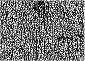
- FIG. 2 is a stereomicrograph of the surface of the electromagnetic wave transmitting metal coating obtained in Example 1.
- FIG. 3 is a stereomicrograph of the surface of the metal coating obtained in Comparative Example 1.
- 4 is a stereomicrograph of the surface of the electromagnetic wave transmitting metal coating obtained in Example 2.
- FIG. 4 is a stereomicrograph of the surface of an electromagnetic wave transmitting metal coating obtained in Example 3.
- An electromagnetic wave transmitting metal coating 100 is a metal coating 20 provided on the surface of a base material 10, which has a metal gloss that is sufficiently metallic in appearance and can transmit electromagnetic waves. is there.
- the electromagnetic wave transmitting metal coating 100 is obtained through an electroless plating process, and as shown in FIG. 1A, a set of fine islands 22 surrounded by fine cracks 21 serving as an electromagnetic wave transmission path. It is structured as a body.
- the fine cracks 21 are formed so as to be distributed substantially uniformly over the entire surface of the metal coating 20.
- the metal film 100 for electromagnetic wave transmission appropriately adjusts the number of the fine islands 22 in the unit area, the width of the fine cracks 21, the thickness of the metal film 20, etc.
- the amount of transmission attenuation can be adjusted, and electromagnetic waves with various wavelengths can be selectively transmitted.
- a description will be given mainly by taking, as an example, a metal film 20 for transmitting millimeter waves that can transmit millimeter waves that enter and exit from a millimeter wave radar device mounted on an automobile or the like.
- Metal coating 20 The metal coating 20 according to the present invention is configured as an aggregate of fine islands 22 surrounded by fine cracks 21, as described above. Two to 10,000 fine islands 22 exist in a unit area (1 mm 2 ). Thus, by covering the surface of the base material 10 discontinuously with the fine islands 22 surrounded by the fine cracks 21, electromagnetic waves can be transmitted through the gaps (fine cracks 21) between the adjacent fine islands 22. In addition, the metal coating 20 can be made to exhibit a sufficient metallic luster in appearance.
- the average island diameter of the fine islands 22 is less than 0.01 ⁇ m, the ratio of the area occupied by the fine cracks 21 on the surface of the base material 10 increases, and the ratio of the area occupied by the fine islands 22 decreases. As a result, the glossiness of the metal coating is lowered, and there is a case where a sufficient metallic luster cannot be expressed in appearance. If the average island diameter of the fine islands 22 exceeds 500 ⁇ m, the area of each fine island 22 increases, and the possibility that electromagnetic waves will enter the fine islands 22 increases. For this reason, the electromagnetic wave transmission attenuation amount of the metal coating 20 increases, and the function as the metal coating 100 for electromagnetic wave transmission may not be sufficiently exhibited.
- the island diameter of one fine island 22 is obtained.
- the island diameter refers to the distance between the ends that is the longest distance from one end to the other end of the fine island 22.
- an island diameter is obtained and an average value thereof is obtained to obtain an average island diameter.
- the island diameter is obtained for all the fine islands 22 existing in the observation field when observed with a scanning electron microscope (1000 magnifications), and the average value is obtained.
- the island diameter may be obtained for all the fine islands 22 existing in the unit area (for example, 1 mm 2 ), and the average value may be obtained.
- Shape of fine island 22 In the present invention, the shape of the fine island 22 is preferably a polygonal shape. In consideration of disposing the electromagnetic wave transmitting metal coating 100 on a path of millimeter waves entering and exiting the in-vehicle radar device, it is preferable that at least one of the corners is an acute angle. By forming the fine island 22 into a polygonal shape having at least one corner as an acute angle, the acute angle portion functions as an antenna that receives electromagnetic waves, and can serve as a relay point that radiates electromagnetic waves incident on the metal coating 20. Considering that the metal coating 20 is provided for decoration of a design member typified by an automobile emblem, it is preferable that the shape and size of each fine island 22 are substantially the same. When the shape and size of each fine island 22 are uniform, the metal coating 20 can exhibit a superior metallic luster with no gloss unevenness.
- the width of the fine crack 21 is preferably in the range of 0.01 ⁇ m to 100 ⁇ m.
- the millimeter wave can be transmitted through the fine crack 21 from one side of the metal coating 20 to the other side. Millimeter waves can be satisfactorily transmitted from the other surface side to the one surface side. That is, in the thickness direction of the metal coating 20, the metal coating 20 according to the present invention can pass through when the millimeter wave is incident from any direction. Further, by setting the width of the fine crack 21 to 100 ⁇ m or less, the fine crack 21 in the metal coating 20 can be made invisible and the appearance can be kept excellent.
- the fine cracks 21 exist at an interval of 0.1 ⁇ m to 10,000 ⁇ m on an arbitrary straight line on the metal coating 20.
- arbitrary straight line on the metal coating 20 refers to a straight line virtually drawn on the surface of the metal coating 20 in an arbitrary direction.
- the number of the fine islands 22 present in the unit area and the average island diameter are adjusted to be within the above range by setting the interval where the fine cracks 21 are present in the range in an arbitrary straight line on the metal film 20.
- the shape of the fine islands 22 can be made substantially uniform.
- by setting the interval at which the microcracks 21 are present within this range it is possible to eliminate the uneven electromagnetic wave transmission over the entire surface of the metal coating 20.
- 1 to 10,000 fine cracks 21 exist in a unit area (1 mm 2 ). Since the fine cracks 21 exist in the unit area (1 mm 2 ) in the range of 1 to 10000, the number of the fine islands 22 and the size of the island diameter can be within the above-described ranges.
- the thickness of the metal coating 20 is preferably 0.01 ⁇ m to 1 ⁇ m.
- the film thickness of the metal coating 20 is less than 0.01 ⁇ m, the glossiness is lowered, and there is a case where sufficient metal luster cannot be expressed in appearance.
- the film thickness of the metal coating exceeds 1 ⁇ m, the electromagnetic wave incident on the microcracks 21 between the microislands 22 may enter the end face of the microislands 22 depending on the incident angle, and may be attenuated and become undetectable. For this reason, the function as the electromagnetic wave transmitting metal coating 100 may not be sufficiently exhibited.
- the metal coating 20 is preferably made of one selected from nickel, nickel alloy, copper, copper alloy, silver, silver alloy, tin, tin alloy, gold and gold alloy. These metals are easily available and cheaper than indium. Moreover, when these metals are formed to a film thickness having a sufficient metallic luster in appearance by a vacuum vapor deposition method, a continuous film is formed and electromagnetic wave permeability is lost. On the other hand, in the present invention, by employing an electroless plating method, it is possible to obtain a metal film 20 having an electromagnetic wave permeability while exhibiting a sufficient metallic luster in appearance using these inexpensive metals. . Moreover, the design of the member provided with the metal coating 20 can be varied depending on the metal color exhibited by each metal.
- Substrate 10 Next, the substrate 10 according to the present invention will be described.
- the base material 10 on which the metal coating 20 is provided one kind selected from insulating resin, ceramics, paper, glass, and fiber can be used.
- the insulating resin any of a thermoplastic insulating resin and a thermosetting insulating resin may be used, and the material of the resin used as the substrate 10 is not particularly limited.
- the linear expansion coefficient on the base material 10 side is less than 1.01, the difference between the linear expansion coefficient on the base material 10 side and the linear expansion coefficient of the metal coating 20 is small, and even after baking is performed. It becomes difficult to form the fine crack 21 in the metal coating 20.
- the upper limit of the linear expansion coefficient by the side of the base material 10 can be suitably set according to the kind of metal which comprises the metal film 20, it is reasonable to make about 100 times the upper limit.
- the linear expansion coefficient on the base material 10 side exceeds 100 times, the linear expansion coefficient on the base material 10 side is larger than the linear expansion coefficient of the metal film 20, so that a large crack is formed in the metal film 20 during after-baking. There is a fear, and it becomes difficult to form fine cracks uniformly dispersed on the entire surface of the metal coating 20.
- the linear expansion coefficient on the base material 10 side can be adjusted to be within the above-mentioned range.
- the linear expansion coefficient on the substrate 10 side includes the linear expansion coefficient of the base layer 30 provided on the upper surface of the substrate 10.
- many of the insulating resins have a linear expansion coefficient in the above range with respect to the linear expansion coefficient of the metal coating 20.
- the coefficient of linear expansion of ceramics, glass, etc. is low, and may show the same value as the coefficient of linear expansion of the metal constituting the metal coating 20.
- insulating resins examples include ABS (acrylonitrile-butadiene-styrene) resin, AES (acrylonitrile-ethylene-styrene) resin, acrylic resin, polyacetal resin, polyamide resin, polyamideimide resin, polyimide resin, Polyurethane resin, polyester resin, polyethylene resin, polyethylene naphthalate resin, polyethersulfone, polyetheretherketone, liquid crystal polymer (LCP), polyvinyl chloride resin, polyolefin resin, polycarbonate resin, polystyrene resin, polysulfone resin, cellulose resin, polyphenylene Examples thereof include sulfide resins.
- these various listed resins are only examples, and in the present invention, various thermoplastic insulating resins and thermosetting insulating resins can be used as the base material.
- insulating resins listed above one selected from polyester, ABS (acrylonitrile-butadiene-styrene) resin, AES (acrylonitrile-ethylene-styrene) resin, polycarbonate resin, acrylic resin and polyolefin resin may be used. preferable. Since these resins have a linear expansion coefficient several times that of the metal film 20, fine cracks can be satisfactorily formed in the above-described range with respect to the metal film 20 by performing heat treatment. Further, these resins are strong and have good moldability, so that, for example, they can achieve the mechanical strength required when used as automobile parts such as a cover member of an in-vehicle radar device, It can be formed into a desired shape such as an automobile emblem.
- a hydrophilic resin material as a material for forming the base layer 30.
- a hydrophilic resin material it becomes possible to adjust the linear expansion coefficient by the side of the base material 10 in the above-mentioned range.
- the foundation layer 30 formed using such a hydrophilic resin material is water-insoluble. This is to prevent the base layer 30 from eluting into the electroless plating solution or the like when the electroless plating solution or the like constituting the plating bath is brought into contact with the base layer 30.
- the thickness of the foundation layer 30 is less than 0.1 ⁇ m, the ability of the catalyst to adhere is lowered. On the other hand, if the thickness of the underlayer 30 exceeds 1 ⁇ m, the fine crack 21 is hardly generated in the metal coating 20 even after baking.
- an electroless plating solution containing an appropriate metal can be used as appropriate according to the type of the metal coating 20 formed on the surface of the substrate 10. As described above, it is preferable to use at least one selected from nickel, nickel alloy, copper, copper alloy, silver, silver alloy, tin, tin alloy, gold and gold alloy as the metal constituting the metal coating 20.
- the conductive film forming process according to the present invention includes, for example, the following catalyzer process, accelerator process, activator process, and electroless plating process, and by performing each process, a metal is formed on the surface of the substrate 10. By depositing, a conductive film having a metallic luster can be formed.
- each step will be described.
- the catalyzer process is a process of adsorbing or adhering palladium metal as a catalyst to the surface of the base material 10 by bringing the surface of the base material 10 into contact with a colloidal catalyst (catalyzer) of palladium and tin. At this time, a small amount of tin is adsorbed or adhered to the surface of the substrate 10 as a divalent or tetravalent tin salt.
- a cleaning treatment such as a degreasing treatment such as acid / alkali washing
- a conditioning treatment, a pre-dip treatment, or the like may be performed as a pretreatment using a commercially available chemical solution.
- Accelerator step In the accelerator step, an accelerator (accelerator) made of sulfuric acid having a concentration of about 0.1% to 10% or a sodium hydrogen sulfate solution having a concentration of about 0.1 g / l to 400 g / l, and the surface of the substrate 10 Is a step for oxidizing the tin adhering to the surface of the base material 10 (or the underlayer 30) to reduce Pd and promoting an electroless plating reaction performed later. .
- an accelerator an accelerator (accelerator) made of sulfuric acid having a concentration of about 0.1% to 10% or a sodium hydrogen sulfate solution having a concentration of about 0.1 g / l to 400 g / l, and the surface of the substrate 10 Is a step for oxidizing the tin adhering to the surface of the base material 10 (or the underlayer 30) to reduce Pd and promoting an electroless plating reaction performed later.
- the catalyst metal nucleus for depositing metal is uniformly formed on the surface of the substrate 10 (or the underlayer 30) by performing the accelerator process and the activator process. Can be absorbed.
- the fine island film forming process Next, the fine island film forming process will be described.
- the conductive film formed in the conductive film forming step is heat-treated to form a fine crack 21 in the conductive film, and the fine island 22 surrounded by the fine crack 21 has a unit area (1 mm). 2
- the electromagnetic wave transmitting metal coating 100 is formed as an aggregate of the fine islands 22 present in 2 to 10,000. As described above, this heat treatment is referred to as “after baking” in the present invention. Further, in the fine island film forming step, by forming the fine cracks in the unit area (1 mm 2 ) by 1 to 10000 by the after baking, the number of fine islands is within the above range. ing.
- After baking time After baking is preferably performed for 1 to 60 minutes within the above temperature range.
- the after baking time is less than 1 minute, the baking time is short, and it becomes difficult to form the fine cracks 21 in the conductive film formed in the conductive film forming step.
- the fine cracks 21 having a width within the above-mentioned range can be formed at any intervals on the conductive film at the above-mentioned intervals.
- it is possible to carry out after-baking for more than 60 minutes it is reasonable that the after-baking time is 60 minutes or less from an economic point of view. There is a high possibility that the constituent resin of the material 10 or the base layer 30 is deteriorated.
- the in-vehicle radar device (not shown) according to the present invention receives a transmission means for transmitting millimeter waves as a transmission wave and a radio wave reflected by an object such as a preceding vehicle as a reception wave.
- the receiving means the measuring means for measuring the time from when the transmitted wave is transmitted until the received wave is received, the distance from the object based on the time measured by the measuring means, the relative speed with the object, etc.
- a calculation means for calculating is generally disposed on the back side of the exterior member of the vehicle, such as the back side of the front grille of the vehicle.
- the exterior member of a vehicle is usually subjected to metal plating from the viewpoint of design.
- the exterior member in which these in-vehicle radar devices are arranged is provided with an opening for emitting and receiving millimeter waves.
- the on-vehicle radar device according to the present invention includes a cover member for covering such an opening.
- the in-vehicle radar device is arranged behind the emblem 40 (or emblem 50) provided in the center of the front grille in the vehicle width direction, and the front grille emblem 40 (or emblem 50) is attached to the position. The following description will be made on the assumption that an opening for entering and exiting a millimeter wave is formed.
- the metal film for electromagnetic wave transmission of Example 1 was formed through the following underlayer formation process, conductive film formation process, and fine island film formation process in order.
- the base material on which the conductive film was formed was post-baked at 120 ° C. for 30 minutes to obtain an electromagnetic wave transmitting metal coating of Example 1.
- the linear expansion coefficient on the substrate side is 7 ⁇ 10 ⁇ 5
- the linear expansion coefficient of nickel is 1.28 ⁇ 10 ⁇ 5 .
- the glass transition temperature of the substrate is 130 ° C.
- a conductive film was formed on the surface of the substrate by the following steps.
- alkaline degreasing was performed for 3 minutes under the condition of 65 ° C.
- the conditioner was performed for 2 minutes under the condition of 45 ° C.
- the pre-dip was performed for 1 minute under the condition of 45 ° C.
- Catalyzer step In the catalyzer step, the pretreated substrate was immersed in a mixed catalyst (catalyzer; Rohm and Haas) for 5 minutes at 45 ° C.
- a metal film for electromagnetic wave transmission of Example 5 was obtained by the same procedure as Example 4 except that it was immersed in a nickel plating bath until the thickness of the nickel film reached about 140 nm.
- Comparative example 1 A metal film of Comparative Example 1 was obtained in the same procedure as in Example 1 except that the fine island film forming step was not performed in Example 1.
- Comparative example 2 A metal film of Comparative Example 2 was obtained in the same procedure as in Example 5 except that the fine island film forming step was not performed in Example 5.
- FIG. 4 shows a stereomicrograph of the surface of the metal film for electromagnetic wave transmission of Example 1 taken. Further, a stereomicrograph of the surface of the metal coating of Comparative Example 1 is shown in FIG. As shown in FIG. 4, the metal film for transmitting electromagnetic waves obtained in Example 1 has 862 fine islands in a unit area (1 mm 2 ) surrounded by a square shown in FIG. Further, 918 fine cracks exist in the same unit area. In contrast, the metal film obtained in Comparative Example 1 is formed in an island shape, but the number of island-shaped films present in the unit area (1 mm 2 ) is 12, and cracks are not generated. There are twelve in the same unit area.
- the metal film can be formed as an electromagnetic wave transmitting metal film as an aggregate of fine islands in which countless fine islands are aggregated.
- a stereoscopic microscope SZX7 manufactured by Olympus was used for taking the stereoscopic microscope photographs shown in FIGS. 4 and 5, and the magnification was 25 times. Further, the number of fine cracks (and the number of cracks) was counted as follows.
- one fine crack refers to one that does not intersect with other fine cracks in the length direction of the fine cracks and that contacts the end portions of the other fine cracks only at both ends of the fine cracks. . That is, in the present invention, in the length direction of the fine crack, the one having no contact with the end of the other fine crack or the intersection with the other fine crack between both ends thereof is regarded as one fine crack.
- the number of fine cracks present in the unit area was counted. Regarding the cracks, the number of cracks present in the unit area was counted in the same manner as the fine cracks.
- Example 2 a stereoscopic micrograph of the metal film for electromagnetic wave transmission of Example 2 is shown in FIG.
- the stereomicroscope photograph of the metal film for electromagnetic wave transmission of Example 3 is shown in FIG.
- a stereomicroscope SZX7 manufactured by Olympus Corporation was used for taking the SEM photograph, as in FIGS.
- the electromagnetic wave transmitting metal film obtained in Example 2 and Example 3 also has an infinite number of fine cracks formed in the vertical and horizontal directions as in Example 1.
- a metal film for electromagnetic wave transmission as an aggregate could be obtained.
- the electromagnetic wave transmission attenuation amount of the electromagnetic wave transmission metal coating itself of Example 4 is -0.9 dB
- the electromagnetic wave transmission attenuation amount of Example 5 of the electromagnetic wave transmission metal coating itself is -1.19 dB. Met.
- the electromagnetic wave transmission attenuation of the metal coating of Comparative Example 2 was -13.36 dB.
- the metal film for electromagnetic wave transmission according to the present invention has a very small transmission attenuation amount of electromagnetic waves at 76 GHz, and is a metal that decorates a cover member such as an emblem disposed on the millimeter wave path of the millimeter wave radar device, for example. It can be suitably used as a film.
Landscapes
- Chemical & Material Sciences (AREA)
- Engineering & Computer Science (AREA)
- Metallurgy (AREA)
- Chemical Kinetics & Catalysis (AREA)
- Materials Engineering (AREA)
- Mechanical Engineering (AREA)
- General Chemical & Material Sciences (AREA)
- Organic Chemistry (AREA)
- Inorganic Chemistry (AREA)
- Remote Sensing (AREA)
- Chemically Coating (AREA)
- Details Of Aerials (AREA)
- Radar Systems Or Details Thereof (AREA)
Abstract
外観上、十分な金属光沢を有する電磁波透過用金属被膜を提供するとともに、当該電磁波透過用金属被膜の形成に最適な電磁波透過用金属被膜の形成方法を提供することを目的とする。 この目的を達成するために、無電解めっき工程を経て得られた、電磁波の透過パスとなる微細クラックに囲まれた微細アイランドの集合体であって、金属光沢を有し、前記微細アイランドが単位面積(1mm2)中に2個~10000個存在する金属被膜を電磁波透過用金属被膜として基材の表面に設ける。
Description
本件発明は、金属光沢を有し、かつ、電磁波透過性を有する電磁波透過用金属被膜、電磁波透過用金属被膜の形成方法及び当該金属被膜を備えたカバー部材を有する車載用レーダー装置に関する。
従来より、電磁波透過性が要求される部材を装飾するために、真空蒸着法により基材の表面にインジウムをアイランド状に成膜したインジウム被膜を部材に設けることが行われている。アイランド状に成膜されたインジウム被膜は、金属光沢を有するとともに、アイランド間の隙間を電磁波の透過パスとすることができる。このため、インジウム被膜は、例えば、エンブレム等、自動車に搭載されるミリ波レーダー装置のカバー部材を装飾する金属被膜として用いられている(例えば、「特許文献1」及び「特許文献2」参照)。
しかし、インジウムは高価な金属であるため、インジウムの使用量を削減した電磁波透過用金属被膜、あるいはインジウム以外の金属を用いた電磁波透過用金属被膜が求められている。
そこで、樹脂基材の表面にインジウムを真空蒸着して形成した第1膜を設け、この第1膜の上面にクロムを真空蒸着により成膜した第2膜を設けることにより、インジウムの使用量を削減することが行われている(例えば、「特許文献3」参照)。
一方、現時点では、真空蒸着法により形成されたインジウムのアイランド状被膜以外の電磁波透過用金属被膜であって、実用に耐え得るレベルの電磁波透過性を有するとともに、外観上、十分な金属光沢を有する電磁波透過用金属被膜は知られていない。
本件発明は、インジウム以外の金属を用いて、外観上、十分な金属光沢を有する電磁波透過用金属被膜を提供するとともに、当該電磁波透過用金属被膜の形成に最適な電磁波透過用金属被膜の形成方法及び当該電磁波透過用金属被膜を用いた車載用レーダー装置を提供することを目的とする。
そこで、本発明者等は、鋭意研究を行った結果、以下の電磁波透過用金属被膜、電磁波透過用金属被膜の形成方法及び車載用レーダー装置を採用することで上記課題を達成するに到った。
本件発明に係る電磁波透過用金属被膜は、基材の表面に設けられた電磁波を透過可能な金属被膜であり、当該金属被膜は、無電解めっき工程を経て得られた、電磁波の透過パスとなる微細クラックに囲まれた微細アイランドの集合体であって、金属光沢を有し、前記微細アイランドが単位面積(1mm2)中に2個~10000個存在することを特徴とする。
本件発明に係る電磁波透過用金属被膜は、前記基材の表面に設けられた前記微細アイランドの平均アイランド径が、走査型電子顕微鏡で観察した際に、0.01μm~500μmであることが好ましい。
本件発明に係る電磁波透過用金属被膜は、前記微細クラックの幅が0.01μm~100μmであることが好ましい。
本件発明に係る電磁波透過用金属被膜は、前記微細クラックが、当該金属被膜上の任意の直線において、0.1μm~10000μmの間隔で存在することが好ましい。
本件発明に係る電磁波透過用金属被膜は、当該金属被膜の膜厚が、0.01μm~1μmであることが好ましい。
本件発明に係る電磁波透過用金属被膜は、当該金属被膜が、前記無電解めっき工程において前記基材の表面に形成された導通膜を加熱処理することにより得られた非導通膜であることが好ましい。
本件発明に係る電磁波透過用金属被膜は、当該金属被膜において、前記微細クラックが単位面積(1mm2)中に1本~10000本存在することが好ましい。
本件発明に係る電磁波透過用金属被膜は、前記基材が、絶縁性樹脂、セラミックス、紙、ガラス及び繊維から選択された一種であることが好ましい。
本件発明に係る電磁波透過用金属被膜は、前記基材の表面に線膨張係数が前記金属被膜よりも高い親水性樹脂基材を用いて形成された下地層が設けられることが好ましい。
本件発明に係る電磁波透過用金属被膜は、前記基材側の線膨張係数が、前記金属被膜の線膨張係数に対して、1.01倍以上であることが好ましい。
本件発明に係る電磁波透過用金属被膜は、前記金属被膜が、ニッケル、ニッケル合金、銅、銅合金、銀、銀合金、錫、錫合金、金及び金合金から選択された少なくとも一種を含むことが好ましい。
本件発明に係る電磁波透過用金属被膜の形成方法は、基材の表面に対し、電磁波を透過可能であり、且つ、金属光沢を有する電磁波透過用金属被膜を形成する方法であって、以下の工程を備えることを特徴とする。
(1) 無電解めっき法により、基材の表面に金属光沢を有する導通膜を形成する導通膜形成工程。
(2) 前記導通膜形成工程において形成された導通膜を加熱処理することにより、当該導通膜に電磁波の透過パスとなる微細クラックを形成し、当該微細クラックに囲まれた微細アイランドが単位面積(1mm2)中に2個~10000個存在する微細アイランドの集合体としての前記電磁波透過用金属被膜を形成する微細アイランド被膜形成工程。
(1) 無電解めっき法により、基材の表面に金属光沢を有する導通膜を形成する導通膜形成工程。
(2) 前記導通膜形成工程において形成された導通膜を加熱処理することにより、当該導通膜に電磁波の透過パスとなる微細クラックを形成し、当該微細クラックに囲まれた微細アイランドが単位面積(1mm2)中に2個~10000個存在する微細アイランドの集合体としての前記電磁波透過用金属被膜を形成する微細アイランド被膜形成工程。
また、本件発明に係る電磁波透過用金属被膜の形成方法は、基材の表面に対し、電磁波を透過可能であり、且つ、金属光沢を有する電磁波透過用金属被膜を形成する方法であって、以下の工程を備えることを特徴とする。
(1) 無電解めっき法により、基材の表面に金属光沢を有する導通膜を形成する導通膜形成工程。
(2) 前記導通膜形成工程において形成された導通膜を加熱処理することにより、当該導通膜に電磁波の透過パスとなる微細クラックを単位面積(1mm2)中に1本~10000本形成し、当該金属被膜を微細クラックに囲まれた微細アイランドの集合体としての前記電磁波透過用金属被膜を形成する微細アイランド被膜形成工程。
(1) 無電解めっき法により、基材の表面に金属光沢を有する導通膜を形成する導通膜形成工程。
(2) 前記導通膜形成工程において形成された導通膜を加熱処理することにより、当該導通膜に電磁波の透過パスとなる微細クラックを単位面積(1mm2)中に1本~10000本形成し、当該金属被膜を微細クラックに囲まれた微細アイランドの集合体としての前記電磁波透過用金属被膜を形成する微細アイランド被膜形成工程。
本件発明に係る電磁波透過用金属被膜の形成方法は、前記微細アイランド被膜形成工程において、前記加熱処理を前記基材のガラス転移温度±50℃の範囲内で行うことが好ましい。
本件発明に係る車載用レーダー装置は、上記いずれかに記載の電磁波透過用金属被膜を基材の表面に備えたカバー部材を用いることを特徴とする車載用レーダー装置。
本件発明に係る車載用レーダー装置は、前記カバー部材が、自動車のフロントグリルの車幅方向中央に取り付けられたエンブレムであることが好ましい。
本件発明によれば、無電解めっき法を採用することにより、高価なインジウムに代えて、安価な金属を用いて外観上、十分な金属光沢を有し、且つ、電磁波を透過可能な電磁波透過用金属被膜を提供することができる。
また、本件発明によれば、無電解めっき法を採用しているため、真空蒸着法によりアイランド状の金属被膜を形成する場合と異なり、真空設備等の設備コストを低減することができる。また、真空蒸着法と異なり、真空容器の内部で成膜する必要がないため、当該電磁波透過用金属被膜を設ける基材の大きさが真空容器内に収容可能な大きさに限定されるなどの基材の大きさに関する制約が少ない。また、無電解めっき法を採用しているため、基材の形状に対する制約が少なく、複雑な表面形状を有する基材についても、微細クラックが形成された金属被膜を設けることができる。従って、多様な製品に、外観上、十分な金属光沢を有し、且つ、電磁波を透過可能な金属被膜を設けることができる。
以下、本件発明に係る電磁波透過用金属被膜、電磁波透過用金属被膜の形成方法、車載用レーダー装置及び光透過用電波シールド材の好ましい実施の形態を説明する。
〈電磁波透過用金属被膜〉
まず、図1を参照して、本件発明に係る電磁波透過用金属被膜100について説明する。本件発明に係る電磁波透過用金属被膜100は、基材10の表面に設けられた金属被膜20であって、外観上、十分な金属光沢を有し、且つ、電磁波を透過可能な金属被膜20である。当該電磁波透過用金属被膜100は、無電解めっき工程を経て得られたものであり、図1(a)に示すように、電磁波の透過パスとなる微細クラック21に囲まれた微細アイランド22の集合体として構成されている。微細クラック21は、金属被膜20の全面に略均一に分散するようにして形成されている。本件発明に係る電磁波透過用金属被膜100は、単位面積中の微細アイランド22の数や、微細クラック21の幅、当該金属被膜20の厚み等を適宜調整することにより、当該金属被膜20の電磁波の透過減衰量を調整したり、種々の波長の電磁波を選択的に透過することができる。本実施の形態では、主として、自動車等に搭載されるミリ波レーダー装置から出入射するミリ波を透過可能なミリ波透過用の金属被膜20を例に挙げて説明する。
まず、図1を参照して、本件発明に係る電磁波透過用金属被膜100について説明する。本件発明に係る電磁波透過用金属被膜100は、基材10の表面に設けられた金属被膜20であって、外観上、十分な金属光沢を有し、且つ、電磁波を透過可能な金属被膜20である。当該電磁波透過用金属被膜100は、無電解めっき工程を経て得られたものであり、図1(a)に示すように、電磁波の透過パスとなる微細クラック21に囲まれた微細アイランド22の集合体として構成されている。微細クラック21は、金属被膜20の全面に略均一に分散するようにして形成されている。本件発明に係る電磁波透過用金属被膜100は、単位面積中の微細アイランド22の数や、微細クラック21の幅、当該金属被膜20の厚み等を適宜調整することにより、当該金属被膜20の電磁波の透過減衰量を調整したり、種々の波長の電磁波を選択的に透過することができる。本実施の形態では、主として、自動車等に搭載されるミリ波レーダー装置から出入射するミリ波を透過可能なミリ波透過用の金属被膜20を例に挙げて説明する。
ここで言う単位面積中の微細アイランド22の数は、金属被膜20に形成される微細クラック21の間隔により調整することができる。微細クラック21が形成される間隔や、微細クラック21の幅は、無電解めっき工程により基材10の表面に被膜を形成した後に行う加熱処理により調整することができる。以下、金属被膜20、基材10の順に説明する。以下、本件発明において、無電解めっき工程により基材10の表面に被膜を形成した後に行う加熱処理を「アフターベーキング」と称する。
金属被膜20: 本件発明に係る金属被膜20は、上述した通り、微細クラック21に囲まれた微細アイランド22の集合体として構成されている。この微細アイランド22は、単位面積(1mm2)中に2個~10000個存在している。このように、微細クラック21に囲まれた微細アイランド22で基材10の表面を不連続に覆うことにより、互いに隣接する微細アイランド22間のギャップ(微細クラック21)を介して電磁波を透過可能とすると共に、金属被膜20に、外観上、十分な金属光沢を発現させることができる。
微細アイランド22: ここで、微細アイランド22は、それぞれが基材10に密着した微細な金属被膜であり、互いに微細クラック21を介して他の微細アイランド22に隣接している。微細アイランド22の平均アイランド径は、走査型電子顕微鏡(倍率1000倍)で観察した際に、0.01μm~500μmであることが好ましい。微細アイランド22の平均アイランド径が0.01μm~500μmの範囲内である場合、外観上、十分な金属光沢を発現することができると共に、電磁波透過パスとしての微細クラックが基材10の表面に均一に分散された状態とすることができる。また、微細アイランド22の平均アイランド径が当該範囲内である場合、単位面積(1mm2)中の微細アイランドの数を上述の範囲内にすることができる。
一方、微細アイランド22の平均アイランド径が0.01μm未満の場合、基材10表面における微細クラック21が占める面積の比率が大きくなり、微細アイランド22が占める面積の割合が低下する。その結果、金属被膜の光輝性が低下し、外観上十分な金属光沢を発現することができない場合がある。また、微細アイランド22の平均アイランド径が500μmを超えると、一つ一つの微細アイランド22の面積が大きくなり、電磁波が当該微細アイランド22に入射する可能性が高くなる。このため、当該金属被膜20の電磁波透過減衰量が増加し、電磁波透過用金属被膜100としての機能を十分に発揮することができなくなる場合がある。
次に、平均アイランド径の算出方法を説明する。まず、一つの微細アイランド22のアイランド径を求める。ここで、アイランド径は、微細アイランド22の一端から他端までの距離で最長となる端部間の距離を指す。あるいは、画像処理装置を用いる等して、当該微細アイランド22の面積と等しくなる円の直径を算出して得られる近似径を使用することも可能である。複数の微細アイランド22について、それぞれアイランド径を求め、その平均値を求めることにより、平均アイランド径が得られる。但し、平均アイランド径を求める際に、例えば、走査型電子顕微鏡(倍率1000倍)で観察した際の観察視野中に存在する微細アイランド22の全てについて、それぞれアイランド径を求め、その平均値を求めてもよいし、単位面積中(例えば、1mm2)に存在する微細アイランド22の全てについて、それぞれアイランド径を求め、その平均値を求めてもよい。
微細アイランド22の形状: 本件発明において、微細アイランド22の形状は、多角形状であることが好ましい。また、当該電磁波透過用金属被膜100を車載用レーダー装置に対して出入射するミリ波の経路上に配置することを考慮した場合、少なくとも一つの角が鋭角であることが好ましい。微細アイランド22が、少なくとも一つの角を鋭角とする多角形状とすることにより、鋭角部分が電磁波を受信するアンテナとして機能し、当該金属被膜20に入射した電磁波を放射する中継点とできる。また、自動車用エンブレムに代表される意匠部材の装飾のために当該金属被膜20が設けられる点を考慮すると、各微細アイランド22の形状及び大きさが略同一であることが好ましい。各微細アイランド22の形状及び大きさが揃っていると、金属被膜20はより光沢ムラのない秀麗な金属光沢を発現することができる。
微細クラック21: 本件発明において、微細クラック21の幅は、0.01μm~100μmの範囲であることが好ましい。微細クラック21の幅を0.01μm以上とすることにより、当該微細クラック21を介してミリ波を金属被膜20の一面側から他面側に良好に透過させることができ、また、金属被膜20の他面側から一面側にミリ波を良好に透過させることができる。すなわち、金属被膜20の厚み方向において、いずれの方向からミリ波が入射した場合でも、本件発明に係る金属被膜20はこれを透過することができる。また、微細クラック21の幅を100μm以下とすることで、当該金属被膜20における微細クラック21を視認不能とし、外観を秀麗に保つことができる。
さらに、微細クラック21は、金属被膜20上の任意の直線において、0.1μm~10000μmの間隔で存在することが好ましい。但し、「金属被膜20上の任意の直線」とは、金属被膜20の表面上に任意の方向に仮想的に引かれた直線を指す。金属被膜20上の任意の直線において、微細クラック21が存在する間隔を当該範囲とすることにより、上述した微細アイランド22が単位面積中に存在する数及び平均アイランド径を上述の範囲内に調整することができ、また、微細アイランド22の形状を略均一にすることができる。また、微細クラック21が存在する間隔を当該範囲とすることにより、金属被膜20の表面全面における電磁波透過性の偏りを無くすことができる。
また、微細クラック21は単位面積(1mm2)中に1本~10000本存在することが好ましい。微細クラック21が単位面積(1mm2)中に1本~10000の範囲で存在することにより、微細アイランド22の数やアイランド径の大きさを上述の範囲内にすることができる。
金属被膜20の膜厚: 本件発明において、金属被膜20の膜厚は、0.01μm~1μmであることが好ましい。金属被膜20の膜厚が0.01μm未満である場合、光輝性が低下し、外観上、十分な金属光沢を発現することができない場合がある。一方、金属被膜の膜厚が1μmを超えると、微細アイランド22間の微細クラック21に入射した電磁波が、その入射角によっては微細アイランド22の端面に入射し、減衰して検出不能となる場合があることから、電磁波透過用金属被膜100としての機能を十分に発揮することができなくなる場合がある。
以上の金属被膜20は、ニッケル、ニッケル合金、銅、銅合金、銀、銀合金、錫、錫合金、金及び金合金から選択された一種から成ることが好ましい。これらの金属は、インジウムと比較して入手が容易であり、且つ、安価である。また、真空蒸着法により、これらの金属を基材に対して外観上、十分な金属光沢を有する膜厚まで成膜した場合、連続膜となってしまい、電磁波透過性が無くなる。一方、本件発明では、無電解めっき法を採用することにより、これらの安価な金属を用いて、外観上、十分な金属光沢を発現させると共に、電磁波透過性を有する金属被膜20を得ることができる。また、それぞれの金属が呈する金属色によって、当該金属被膜20が設けられる部材の意匠を多種多様なものとすることができる。
基材10: 次に、本件発明に係る基材10について説明する。上記の金属被膜20が設けられる基材10として、絶縁性樹脂、セラミックス、紙、ガラス及び繊維から選択された一種を用いることができる。また、絶縁性樹脂としては、熱可塑性絶縁性樹脂及び熱硬化性絶縁性樹脂のいずれを用いてもよく、基材10として用いる樹脂の材質は特に限定されるものではない。
本件発明では、上記いずれの種類の材料から構成された基材10を用いることができるが、基材10側の線膨張係数は、金属被膜20を構成する金属の線膨張係数に対して1.01倍以上であることが好ましい。基材10側の線膨張係数が、金属被膜20の線膨張係数の1.01倍以上であることにより、アフターベーキング時の基材10側の熱膨張変形に、金属被膜20の熱膨張変形が追従することができない。その結果として、金属被膜20に、電磁波透過に適した適正な微細クラックを形成することができる。ここで、基材10側の線膨張係数が1.01倍未満である場合、基材10側の線膨張係数と、金属被膜20の線膨張係数との差が小さく、アフターベーキングを行っても金属被膜20に微細クラック21を形成するのが困難になる。また、基材10側の線膨張係数の上限は、金属被膜20を構成する金属の種類に応じて適宜設定することができるが、100倍程度を上限とすることが妥当である。基材10側の線膨張係数が100倍を超えると、基材10側の線膨張係数が金属被膜20の線膨張係数に対して大きいため、アフターベーキング時に金属被膜20に大きなクラックが形成される恐れがあり、微細なクラックを金属被膜20の全面に均一に分散させて形成するのが困難になる。
ここで、基材10自体の線膨張係数が低く、基材10自体の線膨張係数が、金属被膜20の線膨張係数に対して上述の範囲内にない場合は、次に説明する下地層30を設けることにより、基材10側の線膨張係数が上述の範囲内となるように調整することができる。但し、基材10側の線膨張係数には、基材10の上面に設けられた下地層30の線膨張係数を含む。例えば、絶縁性樹脂の多くは、金属被膜20の線膨張係数に対して、上述の範囲の線膨張係数を有する。一方、セラミックス、ガラスなどの線膨張係数は低く、金属被膜20を構成する金属の線膨張係数と同様の値を示す場合がある。従って、これらのセラミックス、ガラスなどの線膨張係数が低い材料を基材10として用いる場合には、基材10の表面に線膨張係数が金属被膜20よりも高い親水性樹脂材料を用いて形成した下地層30を設けて、基材10側の線膨張係数を上述の範囲内に調整することが好ましい。また、基材10として絶縁性樹脂等、基材10自体の線膨張係数が上述の範囲内にある材料を基材10として用いた場合でも、下地層30を設けてもよいのは勿論である。なお、下地層30については、後述する。
基材10として、絶縁性樹脂を用いる場合、上記と同様の観点から、線膨張係数が金属被膜20の線膨張係数に対して1.01倍以上のものを用いることが好ましい。このような絶縁性樹脂として、上述した通り、熱可塑性樹脂及び熱硬化性樹脂のいずれも使用することができる。基材10として使用可能な絶縁性樹脂の一例として、ABS(アクリロニトリル-ブタジエン-スチレン)樹脂、AES(アクリロニトリル-エチレン-スチレン)樹脂、アクリル樹脂、ポリアセタール樹脂、ポリアミド樹脂、ポリアミドイミド樹脂、ポリイミド樹脂、ポリウレタン樹脂、ポリエステル樹脂、ポリエチレン樹脂、ポリエチレンナフタレート樹脂、ポリエーテルスルホン、ポリエーテルエーテルケトン、液晶ポリマー(LCP)、ポリ塩化ビニル樹脂、ポリオレフィン樹脂、ポリカーボネート樹脂、ポリスチレン樹脂、ポリスルホン樹脂、セルロース樹脂、ポリフェニレンスルフィド樹脂等を挙げることができる。但し、これら列挙した各種樹脂は、一例に過ぎず、本件発明では、基材として、種々の熱可塑性絶縁性樹脂及び熱硬化性絶縁性樹脂を用いることができる。
以上列挙した絶縁性樹脂の中でも、特に、ポリエステル、ABS(アクリロニトリル-ブタジエン-スチレン)樹脂、AES(アクリロニトリル-エチレン-スチレン)樹脂、ポリカーボネート樹脂、アクリル樹脂及びポリオレフィン樹脂から選択された一種を用いることが好ましい。これらの樹脂は、線膨脹係数が金属皮膜20の数倍程度の値を有するため、加熱処理を行うことにより金属皮膜20に対して、上述の範囲で微細クラックを良好に形成することができる。また、これらの樹脂は、強固であり、成形性が良好であるため、例えば、車載用レーダー装置のカバー部材等の自動車部品として用いる際に要求される機械強度を達成することができ、また、自動車のエンブレム等、所望の形状に成形することができる。
上述した基材10の形状は特に限定はなく、板材、シート材、フィルム材等の他、上述した自動車のエンブレム等、立体形状のものを用いることもできる。本件発明に係る電磁波透過用金属被膜100は、無電解めっき工程を経て得られたものであるため、複雑な立体形状を有する基材10であっても、基材10の表面全面に精度よく金属被膜20を形成することができる。
下地層30: ここで言う下地層30は、基材10側の線膨張係数が上述の要件を満たさない場合に、基材10の表面に補助的に設ける必要のあるものである。また、基材10側の線膨脹係数が低く、熱処理時に変形を伴う場合に、基材10の変形開始温度(軟化点)よりも低温で加熱処理(アフターベーキング)を行う際にも、下地層30が補助的に設けられる。このように、下地層30を補助的に基材10の表面に設けることにより、基材10の軟化点よりも低温でアフターベーキングにより金属被膜20に微細クラック21を形成して、基材10の変形を防止することができる。
当該下地層30を形成する材料は、上述した通り、親水性樹脂材料を用いることが好ましい。このように親水性樹脂材料を用いて下地層30を形成することにより、基材10側の線膨張係数を上述の範囲内に調整することが可能になる。また、このような親水性樹脂材料を用いて形成した下地層30は、非水溶性であることがより好ましい。めっき浴を構成する無電解めっき液等と、下地層30とを接触させた場合、下地層30が無電解めっき液等に溶出するのを防止するためである。
また、親水性樹脂材料を用いて下地層30を形成することにより、基材10の表面が平滑であっても、当該基材10の表面に触媒活性を有する金属粒子を吸着若しくは付着させ、均一な触媒層の形成が容易になる。その結果、均一な触媒層が置換析出して得られる金属被膜20は、基材10に対して良好な密着性を備えるものとなる。また、下地層30を設けることにより、基材10と金属被膜20との密着性を向上させることで、アフターベーキングにより、金属被膜20の表面全面に微細なクラックを略均一に分散させることができる。すなわち、アフターベーキング時には、下地層30と金属被膜20とは、それぞれの線膨張係数に応じて膨張挙動を起こす。このときの線膨張係数の差異を利用して、金属被膜20の微細クラック21を調整する。従って、基材10と金属被膜20との密着不良部位を無くすことで、アフターベーキング時の微細クラック21を金属被膜20の面内に均一に形成することが可能となる。また、金属被膜20の表面全面に微細なクラックを略均一に分散させることで、微細アイランド22の形状や大きさ、アイランド径等のバラツキを低減することができる。
なお、念のために述べておくが、仮に、基材10側の線膨張係数が上述の要件を満たしている場合であっても、当該基材10の表面に補助的に設けても差し支えのないものである。例えば、絶縁性樹脂等の線膨張係数が上述の範囲内である材料を基材10として用いた場合でも、基材10の表面に当該下地層30を設けて、基材10側の線膨張係数を好ましい値あるいは最適な値に調整するとともに、基材10と金属被膜20との密着性を向上して、金属被膜20に形成される微細クラック21を均一に分散させ、かつ、微細クラック21が形成される間隔や微細クラック21の幅を上述の範囲内に調整することが容易になる。
親水性樹脂材料として、例えば、非水溶性ポリエステル樹脂(例えば、WO2008/096671参照)、水酸基を有する樹脂及びイソシアネート系化合物、水酸基を含有してなる親水性及び/又は水溶性樹脂(例えば、特願2006-80942;WO2007/108351参照)等を用いることができる。これらの親水性樹脂材料は非水溶性であることが好ましいが、水溶性である場合には硬化処理を行う等して、非水溶性にすることが好ましい。無電解めっき工程において基材10を触媒液や無電解めっき液に接触させた際に、下地層30が触媒液や無電解めっき液に溶出することを防止し、下地層30の剥離を防止することができる。さらに、触媒液や無電解めっき液に対する下地層30の溶出を防止することにより、触媒液や無電解めっき液を長寿命化することができる。
また、非水溶性ポリエステル樹脂を用いて下地層30を形成することにより、無電解めっき工程の段階で、予め基材10の表面に、一定のレベルで金属をアイランド状に析出させることができる。このときの析出後のアイランド形状は、アイランド径のバラツキが大きく、且つ、電磁波透過用被膜として工業生産性を満足するレベルのものではない。しかし、予め基材10の表面に一定のレベルで金属がアイランド状に析出していれば、事後的に行うアフターベーキングによって、金属被膜20に電磁波透過に適した微細クラック21を導入することが容易になる。このときの非水溶性ポリエステル樹脂の数平均分子量は、2000~30000であることが好ましい。数平均分子量が2000以上のポリエステル樹脂を用いて下地層30を形成することにより、下地層30を強い被膜とすることができる。また、数平均分子量が30000以下のポリエステル樹脂を用いて下地層30を形成することにより、フィルム状の基材10を使用する場合の下地層30形成後のカール現象の発生を防止することができる。このような非水溶性ポリエステル樹脂として、具体的には、高松油脂社製の自己架橋タイプの非水溶性ポリエステル樹脂(ペスレジンwac-15x、ペスレジンwac-17x)、互応化学社製の非水溶性ポリエステル樹脂(プラスコートZ-850、Z-730、RZ-570)等を用いることができる。
また、下地層30を形成する場合、非水溶性ポリエステル樹脂と他の樹脂とを混合した樹脂組成物を使用してもよい。具体的には、他の樹脂として、ポリビニルブチラール、アクリル系樹脂、ポリウレタン系樹脂などを用いることができる。これらのポリエステル樹脂以外の樹脂は、当該樹脂組成物として非水溶性の特性を維持できる限り、親水性であっても、疎水性であっても構わない。但し、ポリエステル樹脂とともに、ポリエステル樹脂以外の樹脂を用いた樹脂組成物で下地層30を形成する場合には、当該樹脂組成物を100重量%とした場合に、ポリエステル樹脂が50重量%以上含有する組成を採用することが、基材10と金属被膜20との良好な密着性を得るために好ましい。また、基材10と金属被膜20との密着性を、より安定化するためには、当該ポリエステル樹脂成分を80重量%以上含有する組成を採用することがより好ましい。更に、工業的生産における製造バラツキの存在を考慮すると、当該ポリエステル樹脂成分を90重量%以上含有する組成を採用することが、最も好ましい。
下地層30は、上述した非水溶性ポリエステル樹脂と、その他必要に応じて添加する他の樹脂とを適当な溶媒に溶解させた塗布液を、ディップやバーコーティング法などの公知の塗工法により基材10上に塗布し、乾燥することにより形成することができる。また、スプレー塗布後、乾燥することにより下地層30を形成してもよい。あるいは、樹脂を用いて基材10を構成する場合は、基材10を構成する樹脂材料と、下地層30を構成する非水溶性ポリエステル樹脂等とを共押し出しして成形することなどにより下地層30を形成してもよい。
下地層30の厚み: 以上のようにして形成された下地層30の厚みは、ポリエステル樹脂を構成するモノマーの種類などにより異なるが、0.05μm~2μmの範囲が好ましく、0.1μm~1μmの範囲がより好ましい。基材10の表面に当該範囲の厚みの下地層30を設けることにより、親水性樹脂材料の線膨張係数と、金属被膜を構成する金属の線膨張係数との差を利用して、アフターべーキングにより、金属被膜20の全面に微細なクラックを均一に発生させやすくすることができる。
下地層30の厚みが0.1μm未満となると、触媒の付着能が低下する。一方、下地層30の厚みが1μmを超えると、アフターベーキングを行っても金属被膜20に微細クラック21が発生し難くなる。
〈電磁波透過用金属被膜の形成方法〉
次に、上記電磁波透過用金属被膜100の形成方法を説明する。本件発明に係る電磁波透過用金属皮膜100は、下記の工程により形成することが好ましい。以下の工程を採用することによりインジウム以外の金属を用いて、本件発明に係る電磁波透過用金属皮膜100を簡易に製造することができる。
(1) 無電解めっき法により、基材10の表面に金属光沢を有する導通膜を形成する導通膜形成工程。
(2) 導通膜形成工程において形成された導通膜をアフターベーキングすることにより、当該導通膜に電磁波の透過パスとなる微細クラック21を形成し、当該微細クラック21に囲まれた微細アイランド22が単位面積(1mm2)中に2個~10000個存在する微細アイランド22の集合体としての電磁波透過用金属被膜100を形成する微細アイランド被膜形成工程。
次に、上記電磁波透過用金属被膜100の形成方法を説明する。本件発明に係る電磁波透過用金属皮膜100は、下記の工程により形成することが好ましい。以下の工程を採用することによりインジウム以外の金属を用いて、本件発明に係る電磁波透過用金属皮膜100を簡易に製造することができる。
(1) 無電解めっき法により、基材10の表面に金属光沢を有する導通膜を形成する導通膜形成工程。
(2) 導通膜形成工程において形成された導通膜をアフターベーキングすることにより、当該導通膜に電磁波の透過パスとなる微細クラック21を形成し、当該微細クラック21に囲まれた微細アイランド22が単位面積(1mm2)中に2個~10000個存在する微細アイランド22の集合体としての電磁波透過用金属被膜100を形成する微細アイランド被膜形成工程。
[導通膜形成工程]
次に、本件発明に係る導通膜形成工程について説明する。導通膜形成工程では、無電解めっき法により、基材10の表面に金属を析出させて、基材10の表面に金属光沢を有する導通膜を形成する。本件発明では、無電解めっき法により、基材10の表面に金属を析出させることで、膜厚が均一で、緻密な金属被膜20を基材10の表面に精度よく形成することができる。
次に、本件発明に係る導通膜形成工程について説明する。導通膜形成工程では、無電解めっき法により、基材10の表面に金属を析出させて、基材10の表面に金属光沢を有する導通膜を形成する。本件発明では、無電解めっき法により、基材10の表面に金属を析出させることで、膜厚が均一で、緻密な金属被膜20を基材10の表面に精度よく形成することができる。
ここで、基材10として、上述した通り、絶縁性樹脂、セラミックス、紙、ガラス、繊維等、種々の材料から構成された基材を用いることができる。但し、基材10側の線膨張係数は、導通膜を構成する金属の線膨張係数に対して1.01倍以上であることが好ましい。また、基材10側の線膨脹係数の上限値としては、上記と同様の理由から100倍程度であることが好ましい。さらに、上述した理由と同様の理由から、セラミックス、ガラス等の線膨張係数の低い材料を基材10として用いる場合には、線膨張係数が前記金属被膜よりも高い親水性樹脂材料を用いて基材10の表面に下地層30を形成した上で上記導通膜を形成することが好ましい。また、絶縁性樹脂等の線膨張係数が上述した範囲内にある材料を基材10として用いる場合であっても、上述した理由と同様の理由から、線膨張係数が1.01倍以上の親水性樹脂材料を用いて基材10の表面に下地層30を設け、基材10側の線膨張係数を好ましい値あるいは最適な値に調整することがより好ましい。
導通膜形成工程では、基材10の表面に形成する金属被膜20の種類に応じて、適宜、適切な金属を含む無電解めっき液を用いることができる。金属被膜20を構成する金属として、上述した通り、ニッケル、ニッケル合金、銅、銅合金、銀、銀合金、錫、錫合金、金及び金合金から選択された少なくとも一種を用いることが好ましい。
また、本件発明に係る導通膜形成工程は、例えば、以下のキャタライザー工程と、アクセラレータ工程と、アクチベータ工程と、無電解めっき工程とを備え、各工程を行うことにより基材10の表面に金属を析出させて、金属光沢を有する導通膜を成膜することができる。以下、各工程毎に説明する。
キャタライザー工程: キャタライザー工程は、基材10の表面と、パラジウム及びスズのコロイド触媒(キャタライザー)とを接触させることにより、基材10の表面に触媒としてのパラジウム金属を吸着若しくは付着させる工程である。このとき、少量のスズが2価又は4価のスズ塩として基材10の表面に、吸着若しくは付着する。但し、基材10に触媒を付与する際に、前処理として酸/アルカリ洗浄等の脱脂処理等の清浄化処理を行うことが好ましい。その他、必要に応じて、前処理として、市販の薬液を用いて、コンディショニング処理、プレディップ処理等を行ってよいのは勿論である。
また、基材10の表面が平滑であり、触媒がうまく付着しない場合には、機械的処理、化学的処理又は光学的処理(UV処理、プラズマ処理等)等によって、基材10の表面を粗面化するなどの前処理を行ってもよい。また、基材10の触媒付着能を向上するために、上述した親水性樹脂材料を用いて形成した下地層30を設けてもよい。当該下地層30を設けることにより、金属被膜20への微細クラック形成能を向上させるとともに、当該下地層30を触媒付着層として機能させることができ、触媒を良好に付与することができる。
当該工程で用いるコロイド触媒は、例えば、スズの水和物とパラジウムの水和物とを水に溶解させ、その後界面活性剤を加えて十分に撹拌を行いながら、ここに還元剤を添加する方法等、従来既知の方法により調整することができる。また、一般にキャタライザーとして市販されているものを用いることもできる。あるいは、コロイド触媒に代えて、スズ水溶液に基材10を浸漬後、パラジウム水溶液に基材10を浸漬してもよい。
アクセレータ工程: アクセレータ工程では、濃度が0.1%~10%程度の硫酸若しくは、0.1g/l~400g/l程度の硫酸水素ナトリウム溶液からなる促進剤(アクセラレータ)と基材10の表面とを接触させることにより、基材10(又は下地層30)の表面に付着しているスズを酸化させて、Pdを還元し、事後的に行う無電解めっき反応を促進化するための工程である。
アクチベーター工程: アクチベーター工程は、必須の工程ではないが、0.1g/l程度~1g/lの塩化パラジウム溶液と、基材10の表面とを接触させることにより、めっき初期析出をより均一的に反応させる為に行ってもよい。
以上のように、本件発明では、キャタライザー工程後に、アクセレータ工程と、アクチベーター工程とを行うことにより、金属を析出させるための触媒金属核を、基材10(若しくは下地層30)の表面に均一に吸着させることができる。
無電解めっき工程: 次に無電解めっき法により、基材10の表面に金属被膜を析出形成する。当該工程では、金属被膜20を構成する金属を含む従来既知のめっき浴を構成する無電解めっき液と、上述の基材10とを接触させることにより、基材10(若しくは下地層30)の表面に付着したパラジウム金属を触媒として、基材10(若しくは下地層30)の表面に金属を析出させて、導通膜を形成する。このときに用いる無電解めっき液が含有する金属成分の種類に応じた金属が適宜析出する。
このとき、基材10(若しくは下地層30)の表面に析出させた金属被膜層は、金属光沢を有する状態で、アイランド状に金属が析出する場合がある。しかし、係る段階の金属被膜は、電気的導通性が完全に失われたものではなく、電気的導電性を備えるものである。この場合も、次に説明する微細アイランド被膜形成工程において、アフターベーキングを行うことにより、無電解めっきにより形成した金属被膜を構成するアイランド状の析出状態を、更に微細化して電気的導通性の無い微細アイランド状に分割して、単位面積(1mm2)中に存在する微細アイランドの個数を2個~10000個とすることができる。
[微細アイランド被膜形成工程]
次に、微細アイランド被膜形成工程を説明する。微細アイランド被膜形成工程では、導通膜形成工程において形成した導通膜を加熱処理することにより、当該導通膜に微細クラック21を形成し、この微細クラック21に囲まれた微細アイランド22が単位面積(1mm2)中に2個~10000個存在する微細アイランド22の集合体としての電磁波透過用金属被膜100を形成する。上述したように、この加熱処理を、本件発明においては「アフターベーキング」と称している。また、当該微細アイランド膜形成工程では、当該アフターベーキングにより、当該微細クラックを単位面積(1mm2)中に1本~10000本形成させることにより、微細アイランドの数を上述の範囲内となるようにしている。
次に、微細アイランド被膜形成工程を説明する。微細アイランド被膜形成工程では、導通膜形成工程において形成した導通膜を加熱処理することにより、当該導通膜に微細クラック21を形成し、この微細クラック21に囲まれた微細アイランド22が単位面積(1mm2)中に2個~10000個存在する微細アイランド22の集合体としての電磁波透過用金属被膜100を形成する。上述したように、この加熱処理を、本件発明においては「アフターベーキング」と称している。また、当該微細アイランド膜形成工程では、当該アフターベーキングにより、当該微細クラックを単位面積(1mm2)中に1本~10000本形成させることにより、微細アイランドの数を上述の範囲内となるようにしている。
アフターベーキングの温度: ここで、アフターベーキング時の加熱温度は基材10のガラス転移温度±50℃の範囲内で行うことが好ましい。基材10のガラス転移温度±50℃の範囲内で加熱することにより、基材10の熱膨張変形を良好なものとするとともに、基材10と導通膜を構成する金属との線膨張係数の差を利用して、導通膜の全面に微細クラック21をより均一に分散させて形成することができる。ここで、アフターベーキング時の加熱温度は基材10のガラス転移温度±30℃の範囲内で行うことがより好ましく、基材10のガラス転移温度±10℃の範囲内で行うことが特に好ましい。
アフターベーキングを基材10のガラス転移温度-50℃未満で行った場合、基材10の熱膨張変形が小さく、基材10の表面に形成された導通膜に微細クラック21が形成される間隔が大きくなり、単位面積(1mm2)中に存在する微細アイランドの個数が減少し、電磁波透過減衰量が大きくなる。また、基材10のガラス転移温度+50℃よりも高い温度でアフターベーキングを行った場合、基材10が大きく熱膨張変形し、基材10の熱膨張変形に追従できなくなった導通膜に大きなクラックが形成される恐れがあり、良好な金属光沢が得られなくなるため好ましくない。ここで、基材10の導通膜に上述の範囲内で精度良く上述の範囲内の幅の微細クラック21を導通膜上の任意の直線において上述した間隔で形成するという観点から、アフターベーキング時の加熱温度は基材10のガラス転移温度-30℃以上であることが好ましく、基材10のガラス転移温度-10℃以上であることがさらに好ましい。また、基材10を自動車のエンブレム等の意匠部材や各種の部品として用いる場合、基材10の変形は小さい方が好ましいことから、アフターベーキング時の加熱温度は、基材10のガラス転移温度+30℃以下であることが好ましく、さらには基材10のガラス転移温度+10℃以下であることが好ましい。
アフターベーキングの時間: またアフターベーキングは、上述の温度範囲内において、1分~60分行うことが好ましい。アフターベーキングを行う時間が、1分未満の場合は、ベーキング時間が短く、導通膜形成工程において形成された導通膜に微細クラック21を形成することが困難になる。また、アフターベーキングを1分~60分行うことにより、上述の範囲内の幅の微細クラック21を導通膜上の任意の直線において上述した間隔で形成することができる。なお、60分を超えてアフターベーキングを行うことは可能であるが、経済的観点からアフターベーキングを行う時間は60分以内とすることが妥当であり、60分を超えてアフターベーキングを行うと基材10又は下地層30の構成樹脂が劣化する可能性も高くなる。
〈本件発明に係る電磁波透過用金属被膜の利用態様〉
以上説明した本件発明に係る電磁波透過用金属被膜100は、ミリ波レーダー装置のカバー部材を装飾する金属被膜20として好適に用いることができる。以下、車載用レーダー装置及びカバー部材について説明する。
以上説明した本件発明に係る電磁波透過用金属被膜100は、ミリ波レーダー装置のカバー部材を装飾する金属被膜20として好適に用いることができる。以下、車載用レーダー装置及びカバー部材について説明する。
車載用レーダー装置: 本件発明に係る車載用レーダー装置(図示略)は、ミリ波を送信波として送信する送信手段と、送信波が先行車等の対象物により反射した電波を受信波として受信する受信手段と、送信波を送信してから受信波を受信するまでの時間を計測する計測手段と、計測手段により測定された時間に基づき対象物との距離や、対象物との相対速度等を算出する演算手段等とを備えたものである。このような車載用レーダー装置は、一般に、車両のフロントグリルの裏面側等、車両の外装部材の裏面側に配置される。車両の外装部材は、通常、意匠上の観点から金属めっきが施されている。このため、これらの車載用レーダー装置が配置される外装部材には、ミリ波を出入射するための開口が設けられる。本件発明に係る車載用レーダー装置は、このような開口を覆うためのカバー部材を備えたものである。本実施の形態では、フロントグリルの車幅方向中央に設けたエンブレム40(又はエンブレム50)の後方に車載用レーダー装置を配置するものとし、フロントグリルのエンブレム40(又はエンブレム50)取付位置にはミリ波を出入射するための開口が形成されているものとして、以下説明する。
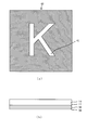
エンブレム: 本件発明に係るカバー部材としてのエンブレム40、50を図2及び図3に示す。図2(a)に示すエンブレム40は、図2(b)に示すように、ポリカーボネート樹脂等の透明の基材10の裏面側に、マスキング部を含む背景色塗布層11と、本件発明に係る金属被膜20層とが順次積層された層構成を有している。背景色塗布層11において、図2(a)に示すエンブレム40を表す意匠部分41は、背景色塗料を塗布する際にマスキングされており、このマスキングされた意匠部分41(マスキング部)には背景色塗料が塗布されていない状態となっている。また、図2(a)に示す例では、「K」の文字で表した部分を「エンブレム40を表す意匠部分41」としている。背景色塗料として、例えば、ミリ波を遮蔽しない黒色塗料を挙げることができるが、背景色は黒に限定されるものではない。図2に示すエンブレム40を構成する基材10は透明であるため、マスキングされた意匠部分41上に設けられた金属被膜20を基材10の表面側から観察することができる。従って、当該エンブレム40を基材10の表面側から観察すると、図示例では「K」の文字を表す意匠部分41にのみニッケル被膜又はニッケル合金被膜が設けられているように見える。基材10を介して金属被膜を観察するため、基材10の表面を粗面化すると、基材10が不透明になる。このため、基材10に対する触媒の付着が良好でない場合には、背景色塗布層11と金属被膜20との間に下地層30を設けてもよい。
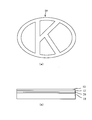
一方、図3(a)に示すエンブレム50は、エンブレム50を表す形状に成形された基材10の表面に本件発明に係る金属被膜20を設けたものであり、図3(b)に示すように、基材10の表面に、本件発明に係る金属被膜20と、意匠塗装層12と、トップコート層13とが順次設けられた層構成を有している。図3(a)に示すエンブレム50は、図2(a)に示すエンブレム40と異なり、基材10の裏面側に金属被膜20を設けるのではなく、基材10の表面に金属被膜20を設ける層構成としているため、不透明の基材10を用いることができる。基材10として、例えば、ABS樹脂、AES樹脂、ポリカーボネート樹脂、シクロオレフィンポリマー等を用いることができる。また、基材10は不透明であってもよいので、基材10の表面を粗してもよい。また、図3(a)に示すエンブレム50の場合であっても、図2に示すエンブレム40と同様に、基材10と金属被膜20との間に下地層30を設けてもよい。
ここで、図2に示すエンブレム40及び図3に示すエンブレム50において、金属被膜20層の層厚は、0.01μm~1μm程度であることが好ましい。上述した通り、当該金属被膜20層の層厚が0.01μm未満の場合は、外観上十分な金属光沢を発現することができない。一方、当該金属被膜20層の層厚が1μmを超える場合は、電磁波透過性が低減する傾向にあり、好ましくない。
以上説明した本実施の形態は、本件発明の一態様であり、本発明の趣旨を逸脱しない範囲において適宜変更可能であるのは勿論である。例えば、上記実施の形態においては、電磁波透過用金属被膜として、ミリ波レーダー装置のミリ波経路上に配置されるカバー部材等を主として説明したが、本件発明に係る電磁波透過用金属被膜はミリ波レーダー装置のカバー部材を装飾する用途に限定されるものではない。上述したように本件発明に係る電磁波透過用金属被膜100は、単位面積中の微細アイランド22の数や、微細クラック21の幅、当該金属被膜20の厚み等を適宜調整することにより、当該金属被膜20の電磁波の透過減衰量を調整したり、種々の波長の電磁波を選択的に透過することができる。例えば、微細クラックの幅を0.01μm~100μmとなるようにアフターベーキング時の条件等を調整することにより、外観上、十分な金属光沢を有し、且つ、光を選択的に透過して、他の外部からの不要な電波を遮断する光透過用電波シールド材として用いることができる。当該光透過用電波シールド材は、例えば、携帯電話等の意匠パネルの装飾皮膜として用いることができ、着信時等を報知する光を透過するとともに、外部からの不要な電波を遮蔽する光透過可能な電波シールド材として利用することができる。
次に、実施例および比較例を示して本件発明を具体的に説明する。但し、本件発明は以下の実施例に限定されるものではない。
下記の下地層形成工程、導通膜形成工程及び微細アイランド被膜形成工程を順次経て、実施例1の電磁波透過用金属被膜を形成した。
〈下地層形成工程〉
本実施例1では、基材として、市販の厚み1000μmのポリカーボネート樹脂を用いた。この基材の一方の面に非水溶性ポリエステル樹脂(プラスコートZ-850:互応化学社)を溶媒で希釈した塗布液をスプレー塗布し、その後、乾燥することにより、厚み1μmの下地層を形成した。
本実施例1では、基材として、市販の厚み1000μmのポリカーボネート樹脂を用いた。この基材の一方の面に非水溶性ポリエステル樹脂(プラスコートZ-850:互応化学社)を溶媒で希釈した塗布液をスプレー塗布し、その後、乾燥することにより、厚み1μmの下地層を形成した。
〈導通膜形成工程〉
(a)キャタライザー工程
次に、下地層が形成された基材を、パラジウム及びスズのコロイド触媒液(キャタライザー;ロームアンドハース:社)に、45℃の条件下で、60秒間浸漬した。
(a)キャタライザー工程
次に、下地層が形成された基材を、パラジウム及びスズのコロイド触媒液(キャタライザー;ロームアンドハース:社)に、45℃の条件下で、60秒間浸漬した。
(b)アクセレータ工程
次に、10%の硫酸(和光純薬社)に、キャタライザー工程を経た基材を45℃の条件下で、30秒浸漬した。
次に、10%の硫酸(和光純薬社)に、キャタライザー工程を経た基材を45℃の条件下で、30秒浸漬した。
(c)アクチベーター工程
次に、0.3g/lの塩化パラジウムに、アクセレータ工程を経た基材を45℃の条件下で、30秒浸漬した。
次に、0.3g/lの塩化パラジウムに、アクセレータ工程を経た基材を45℃の条件下で、30秒浸漬した。
(d)無電解めっき工程
そして、上述のキャタライザー工程、アクセレータ工程、アクチベーター工程を経て、下地層に触媒としてのパラジウム金属が吸着された基材を、45℃、pH8.2に調整したニッケルめっき浴に30秒浸漬し、下地層の表面にニッケルがアイランド状に析出した導通膜を得た。
そして、上述のキャタライザー工程、アクセレータ工程、アクチベーター工程を経て、下地層に触媒としてのパラジウム金属が吸着された基材を、45℃、pH8.2に調整したニッケルめっき浴に30秒浸漬し、下地層の表面にニッケルがアイランド状に析出した導通膜を得た。
〈微細アイランド被膜形成工程〉
微細アイランド被膜形成工程では、導通膜が形成された基材を120℃で30分間アフターベーキングを行い、実施例1の電磁波透過用金属被膜を得た。但し、基材側の線膨張係数は、7×10⁻⁵であり、ニッケルの線膨張係数は1.28×10⁻⁵である。また、基材のガラス転移温度は、130℃である。
微細アイランド被膜形成工程では、導通膜が形成された基材を120℃で30分間アフターベーキングを行い、実施例1の電磁波透過用金属被膜を得た。但し、基材側の線膨張係数は、7×10⁻⁵であり、ニッケルの線膨張係数は1.28×10⁻⁵である。また、基材のガラス転移温度は、130℃である。
実施例2では、基材として、線膨張係数が7×10⁻⁵、ガラス転移温度60℃の樹脂を用いた。そして、下地層を形成せずに、実施例1と同様に導通膜形成工程を行い、基材の表面にニッケルを析出させて、導通膜を形成した。そして、微細アイランド被膜形成工程ではアフターベーキングを75℃の条件下で1時間行った。
〈UV照射工程〉
実施例3では、基材として、ABS樹脂を用いた。当該ABS樹脂の線膨張係数は、7.4×10⁻⁵であり、ガラス転移温度は70℃~90℃の範囲であり、軟化温度は80℃であった。そして、下地層を形成する代わりにUV照射を5分行って基材表面の触媒付着性を向上した。
実施例3では、基材として、ABS樹脂を用いた。当該ABS樹脂の線膨張係数は、7.4×10⁻⁵であり、ガラス転移温度は70℃~90℃の範囲であり、軟化温度は80℃であった。そして、下地層を形成する代わりにUV照射を5分行って基材表面の触媒付着性を向上した。
〈導通膜形成工程〉
次に、下記の工程により基材の表面に導通膜を形成した。まず、前処理としてアルカリ脱脂を65℃の条件下で3分、コンディショナーを45℃の条件下で2分、プレディップを45℃の条件下で1分行った。
次に、下記の工程により基材の表面に導通膜を形成した。まず、前処理としてアルカリ脱脂を65℃の条件下で3分、コンディショナーを45℃の条件下で2分、プレディップを45℃の条件下で1分行った。
(a)キャタライザー工程
キャタライザー工程では、前処理が施された基材を混合キャタリスト(キャタライザー;ロームアンドハース社)に45℃の条件下で5分浸漬した。
キャタライザー工程では、前処理が施された基材を混合キャタリスト(キャタライザー;ロームアンドハース社)に45℃の条件下で5分浸漬した。
(b)アクセレータ工程
次に、10wt%の硫酸(和光純薬社)に、キャタライザー工程を経た基材を45℃の条件下で30秒浸漬した。
次に、10wt%の硫酸(和光純薬社)に、キャタライザー工程を経た基材を45℃の条件下で30秒浸漬した。
(c)アクチベーター工程
次に、アクチベーター(0.3g/l塩化パラジウム水溶液)に、基材を45℃の温度条件下で、30秒浸漬した。
次に、アクチベーター(0.3g/l塩化パラジウム水溶液)に、基材を45℃の温度条件下で、30秒浸漬した。
(d)無電解めっき工程
次に、pH8に調整したNi-Pめっき浴に45℃の条件下で1分間基材を浸漬し、基材の表面にNi-Pが析出した導通膜を得た。
次に、pH8に調整したNi-Pめっき浴に45℃の条件下で1分間基材を浸漬し、基材の表面にNi-Pが析出した導通膜を得た。
〈微細アイランド被膜形成工程〉
微細アイランド被膜形成工程では、導通膜が形成された基材を100℃で30分間アフターベーキングを行い、実施例3の電磁波透過用金属被膜を得た。
微細アイランド被膜形成工程では、導通膜が形成された基材を100℃で30分間アフターベーキングを行い、実施例3の電磁波透過用金属被膜を得た。
基材として、市販の厚み25μmのPETフィルムを用い、この基材の片面に実施例1と同様の手順で導通膜形成工程を行い、基材の表面に約60nmの膜厚のニッケル被膜(導通膜)を形成した。その後、微細アイランド被膜形成工程において80℃の条件下で30分間アフターベーキングを行い、実施例4の電磁波透過用金属被膜を得た。
ニッケル被膜の厚みが約140nmになるまでニッケルめっき浴に浸漬した以外は、実施例4と同様の手順により、実施例5の電磁波透過用金属被膜を得た。
〈比較例1〉
実施例1において微細アイランド被膜形成工程を行わなかったこと以外は、実施例1と同様の手順で比較例1の金属被膜を得た。
実施例1において微細アイランド被膜形成工程を行わなかったこと以外は、実施例1と同様の手順で比較例1の金属被膜を得た。
〈比較例2〉
実施例5において微細アイランド被膜形成工程を行わなかったこと以外は、実施例5と同様の手順で比較例2の金属被膜を得た。
実施例5において微細アイランド被膜形成工程を行わなかったこと以外は、実施例5と同様の手順で比較例2の金属被膜を得た。
〈評価〉
(1)単位面積中に存在する微細アイランドの個数
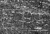
実施例1の電磁波透過用金属被膜の表面を撮影した実体顕微鏡写真を図4に示す。また、比較例1の金属被膜の表面を撮影した実体顕微鏡写真を図5に示す。図4に示すように、実施例1で得た電磁波透過用金属被膜は、図4に示す四角で囲った単位面積(1mm2)中に微細アイランドが862個存在している。また、微細クラックは、同単位面積中に918本存在している。これに対して、比較例1で得た金属被膜は、アイランド状に成膜されているものの、単位面積(1mm2)中に存在するアイランド状の被膜の数は、12個であり、クラックは同単位面積中に12本存在している。このように、微細アイランド被膜形成工程を行うことにより、導通膜形成工程において得た導通膜に微細クラックを導通膜の全面に縦横無尽に無数に形成することができる。その結果、金属被膜を微細アイランドが無数に集合した微細アイランドの集合体としての電磁波透過用金属被膜とすることができる。但し、図4及び図5に示す実体顕微鏡写真の撮影には、それぞれ実体顕微鏡SZX7(オリンパス社製)を用い、倍率は25倍とした。また、微細クラックの数(及びクラックの数)は、次のようにして数えた。まず、本件発明において、1本の微細クラックとは、微細クラックの長さ方向において、他の微細クラックと交差せず、微細クラックの両端部においてのみ他の微細クラックの端部と接するものを指す。すなわち、本件発明では、微細クラックの長さ方向において、その両端部の間に他の微細クラックの端部との接点又は他の微細クラックとの交点のないものを1本の微細クラックとして、上記単位面積中に存在する微細クラックの数を数えた。クラックについても、微細クラックと同様の手法により、上記単位面積中に存在するクラックの数を数えた。
(1)単位面積中に存在する微細アイランドの個数
実施例1の電磁波透過用金属被膜の表面を撮影した実体顕微鏡写真を図4に示す。また、比較例1の金属被膜の表面を撮影した実体顕微鏡写真を図5に示す。図4に示すように、実施例1で得た電磁波透過用金属被膜は、図4に示す四角で囲った単位面積(1mm2)中に微細アイランドが862個存在している。また、微細クラックは、同単位面積中に918本存在している。これに対して、比較例1で得た金属被膜は、アイランド状に成膜されているものの、単位面積(1mm2)中に存在するアイランド状の被膜の数は、12個であり、クラックは同単位面積中に12本存在している。このように、微細アイランド被膜形成工程を行うことにより、導通膜形成工程において得た導通膜に微細クラックを導通膜の全面に縦横無尽に無数に形成することができる。その結果、金属被膜を微細アイランドが無数に集合した微細アイランドの集合体としての電磁波透過用金属被膜とすることができる。但し、図4及び図5に示す実体顕微鏡写真の撮影には、それぞれ実体顕微鏡SZX7(オリンパス社製)を用い、倍率は25倍とした。また、微細クラックの数(及びクラックの数)は、次のようにして数えた。まず、本件発明において、1本の微細クラックとは、微細クラックの長さ方向において、他の微細クラックと交差せず、微細クラックの両端部においてのみ他の微細クラックの端部と接するものを指す。すなわち、本件発明では、微細クラックの長さ方向において、その両端部の間に他の微細クラックの端部との接点又は他の微細クラックとの交点のないものを1本の微細クラックとして、上記単位面積中に存在する微細クラックの数を数えた。クラックについても、微細クラックと同様の手法により、上記単位面積中に存在するクラックの数を数えた。
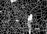
また、実施例2の電磁波透過用金属被膜の実体顕微鏡写真を図6に示す。また、実施例3の電磁波透過用金属被膜の実体顕微鏡写真を図7に示す。但し、当該SEM写真の撮影に際しては、図4及び図5と同様に実体顕微鏡SZX7(オリンパス社製)を用いた。図6及び図7に示すように、実施例2及び実施例3で得た電磁波透過用金属被膜についても、実施例1と同様に微細クラックが縦横無尽に無数に形成されており、微細アイランドの集合体としての電磁波透過用金属被膜が得ることができた。
(2)電磁波透過減衰量
次に、実施例4及び実施例5で得た電磁波透過用金属被膜と、比較例2で得た金属被膜とを用いて、アジレント社製 ネットワークアナライザーを用いて各被膜の76GHzにおける電磁波透過減衰量を評価した。結果を表1に示す。
次に、実施例4及び実施例5で得た電磁波透過用金属被膜と、比較例2で得た金属被膜とを用いて、アジレント社製 ネットワークアナライザーを用いて各被膜の76GHzにおける電磁波透過減衰量を評価した。結果を表1に示す。

表1に示すように、実施例4の電磁波透過用金属被膜自体の電磁波の透過減衰量は-0.9dB、実施例5の電磁波透過用金属被膜自体の電磁波の透過減衰量は-1.19dBであった。一方、比較例2の金属被膜の電磁波の透過減衰量は-13.36dBであった。このように、本件発明に係る電磁波透過用金属被膜は、76GHzにおける電磁波の透過減衰量が極めて小さく、例えば、ミリ波レーダー装置のミリ波経路上に配置されるエンブレム等のカバー部材を装飾する金属被膜として好適に用いることができる。
本件発明に係る電磁波透過用金属被膜100は、無電解めっき法を採用することにより、高価なインジウムに代えて、安価な金属を用いて外観上、十分な金属光沢を有し、且つ、電磁波を透過可能な電磁波透過用金属被膜を、種々の形状の基材の表面に設けることができる。従って、多様な製品に、外観上、十分な金属光沢を有し、且つ、電磁波を透過可能な金属被膜を設けることが可能になる。また、本件発明によれば、単位面積中の微細アイランドの個数、微細クラックの幅等を調整することにより、様々な波長の電磁波を選択的に透過可能としたり、電磁波の透過減衰量の調整が可能になる。このため、光を透過して電波を遮蔽する光透過用電波シールド部材等の種々の新規な用途の金属被膜を提供することができる。
10・・・基材
20・・・金属被膜
30・・・下地層
40、50・・・エンブレム
100・・・電磁波透過用金属被膜
20・・・金属被膜
30・・・下地層
40、50・・・エンブレム
100・・・電磁波透過用金属被膜
Claims (15)
- 基材の表面に設けられた電磁波を透過可能な金属被膜であり、
当該金属被膜は、無電解めっき工程を経て得られた、電磁波の透過パスとなる微細クラックに囲まれた微細アイランドの集合体であって、金属光沢を有し、
前記微細アイランドが単位面積(1mm2)中に2個~10000個存在することを特徴とする電磁波透過用金属被膜。 - 前記基材の表面に設けられた前記微細アイランドの平均アイランド径は、走査型電子顕微鏡で観察した際に、0.01μm~500μmである請求項1に記載の電磁波透過用金属被膜。
- 前記微細クラックの幅が0.01μm~100μmである請求項1又は請求項2に記載の電磁波透過用金属被膜。
- 前記微細クラックは、当該金属被膜上の任意の直線において、0.1μm~10000μmの間隔で存在する請求項1~請求項3のいずれかに記載の電磁波透過用金属被膜。
- 当該金属被膜の膜厚は、0.01μm~1μmである請求項1~請求項4のいずれかに記載の電磁波透過用金属被膜。
- 当該金属被膜は、前記無電解めっき工程において前記基材の表面に形成された導通膜を加熱処理することにより得られた非導通膜である請求項1~請求項5のいずれかに記載の電磁波透過用金属被膜。
- 当該金属被膜において、前記微細クラックが単位面積(1mm2)中に1本~10000本存在することを特徴とする請求項6に記載の電磁波透過用金属被膜。
- 前記基材は、絶縁性樹脂、セラミックス、紙、ガラス及び繊維から選択された一種である請求項1~請求項7のいずれかに記載の電磁波透過用金属被膜。
- 前記基材の基材の表面に線膨張係数が前記金属被膜よりも高い親水性樹脂基材を用いて形成された下地層が設けられる請求項1~請求項8のいずれかに記載の電磁波透過用金属被膜。
- 前記基材側の線膨張係数は、前記金属被膜の線膨張係数に対して、1.01倍以上である請求項1~請求項9のいずれかに記載の電磁波透過用金属被膜。
- 前記金属被膜は、ニッケル、ニッケル合金、銅、銅合金、銀、銀合金、錫、錫合金、金及び金合金から選択された少なくとも一種を含む請求項1~請求項10のいずれかに記載の電磁波透過用金属被膜。
- 基材の表面に対し、電磁波を透過可能であり、且つ、金属光沢を有する電磁波透過用金属被膜を形成する方法であって、
以下の工程を備えることを特徴とする電磁波透過用金属被膜の形成方法。
(1) 無電解めっき法により、基材の表面に金属光沢を有する導通膜を形成する導通膜形成工程。
(2) 前記導通膜形成工程において形成された導通膜を加熱処理することにより、当該導通膜に電磁波の透過パスとなる微細クラックを形成し、当該微細クラックに囲まれた微細アイランドが単位面積(1mm2)中に2個~10000個存在する微細アイランドの集合体としての前記電磁波透過用金属被膜を形成する微細アイランド被膜形成工程。 - 基材の表面に対し、電磁波を透過可能であり、且つ、金属光沢を有する電磁波透過用金属被膜を形成する方法であって、
以下の工程を備えることを特徴とする電磁波透過用金属被膜の形成方法。
(1) 無電解めっき法により、基材の表面に金属光沢を有する導通膜を形成する導通膜形成工程。
(2) 前記導通膜形成工程において形成された導通膜を加熱処理することにより、当該導通膜に電磁波の透過パスとなる微細クラックを単位面積(1mm2)中に1本~10000本形成し、当該金属被膜を微細クラックに囲まれた微細アイランドの集合体としての前記電磁波透過用金属被膜を形成する微細アイランド被膜形成工程。 - 前記微細アイランド被膜形成工程において、前記加熱処理を前記基材のガラス転移温度±50℃で行う請求項12又は請求項13に記載の電磁波透過用金属被膜の形成方法。
- 請求項1~請求項11のいずれかに記載の電磁波透過用金属被膜を基材の表面に備えたカバー部材を用いることを特徴とする車載用レーダー装置。
Applications Claiming Priority (2)
| Application Number | Priority Date | Filing Date | Title |
|---|---|---|---|
| JP2010026632A JP5465030B2 (ja) | 2010-02-09 | 2010-02-09 | 電磁波透過用金属被膜、電磁波透過用金属被膜の形成方法及び車載用レーダー装置 |
| JP2010-026632 | 2010-02-09 |
Publications (1)
| Publication Number | Publication Date |
|---|---|
| WO2011099447A1 true WO2011099447A1 (ja) | 2011-08-18 |
Family
ID=44367721
Family Applications (1)
| Application Number | Title | Priority Date | Filing Date |
|---|---|---|---|
| PCT/JP2011/052519 Ceased WO2011099447A1 (ja) | 2010-02-09 | 2011-02-07 | 電磁波透過用金属被膜、電磁波透過用金属被膜の形成方法及び車載用レーダー装置 |
Country Status (2)
| Country | Link |
|---|---|
| JP (1) | JP5465030B2 (ja) |
| WO (1) | WO2011099447A1 (ja) |
Cited By (4)
| Publication number | Priority date | Publication date | Assignee | Title |
|---|---|---|---|---|
| JP2014179614A (ja) * | 2013-03-13 | 2014-09-25 | Samsung Electronics Co Ltd | 電子装置 |
| WO2015055371A1 (de) * | 2013-10-17 | 2015-04-23 | Robert Bosch Gmbh | Abdeckung für einen radarsensor für kraftfahrzeuge |
| CN104718068A (zh) * | 2012-09-14 | 2015-06-17 | 三惠技研工业株式会社 | 表面光亮品的制造方法 |
| EP3738762A4 (en) * | 2018-01-12 | 2021-10-27 | Nitto Denko Corporation | RADIO-PERMEABLE GLOSSY METAL ELEMENT, ARTICLE THEREFORE AND METHOD OF ITS MANUFACTURING |
Families Citing this family (20)
| Publication number | Priority date | Publication date | Assignee | Title |
|---|---|---|---|---|
| JP5942345B2 (ja) * | 2011-06-10 | 2016-06-29 | 大日本印刷株式会社 | 水圧転写フィルム及び加飾成形品の製造方法 |
| JP5665234B2 (ja) * | 2011-11-04 | 2015-02-04 | 三恵技研工業株式会社 | 電磁波透過用金属被膜及び車載用レーダ装置用のレドーム |
| JP2013253283A (ja) * | 2012-06-06 | 2013-12-19 | Kanto Gakuin | 無電解めっき浴 |
| JP2014145678A (ja) * | 2013-01-29 | 2014-08-14 | Toyota Motor Corp | 装飾被膜 |
| JP6141816B2 (ja) * | 2014-11-10 | 2017-06-07 | 三恵技研工業株式会社 | 電磁波透過用金属被膜及び車載用レーダ装置用のレドーム |
| JP5892629B2 (ja) * | 2014-11-10 | 2016-03-23 | 三恵技研工業株式会社 | 電磁波透過用金属被膜の製造方法 |
| JP2016175348A (ja) * | 2015-03-20 | 2016-10-06 | 日本写真印刷株式会社 | 艶消金属調加飾シートとその製造方法 |
| CN108883607B (zh) * | 2016-04-12 | 2021-09-03 | 索尼公司 | 结构体、电子设备、装饰膜以及结构体的制造方法 |
| WO2018003847A1 (ja) | 2016-06-30 | 2018-01-04 | 日東電工株式会社 | 電磁波透過性金属部材、これを用いた物品、及び、電磁波透過性金属フィルムの製造方法 |
| JP7151700B2 (ja) * | 2017-03-31 | 2022-10-12 | ソニーグループ株式会社 | 構造体、加飾フィルム、構造体の製造方法、及び加飾フィルムの製造方法 |
| KR101810815B1 (ko) * | 2017-04-07 | 2017-12-20 | 김병삼 | 마이크로 크랙 및 레이저 타공홀을 포함하는 전파투과성 센서 커버의 제조 방법 및 이를 이용하여 제조된 전파투과성 센서 커버 |
| KR101824090B1 (ko) * | 2017-04-07 | 2018-03-15 | 김병삼 | 센서 커버용 적층체 |
| JP2019064100A (ja) * | 2017-09-29 | 2019-04-25 | 住友理工株式会社 | 電波透過カバーの製造方法 |
| CN113825858A (zh) * | 2019-05-17 | 2021-12-21 | 希德泰克基金会 | 显示透波性的化学镀金属涂层及其制造方法 |
| WO2022004670A1 (ja) * | 2020-06-30 | 2022-01-06 | 日東電工株式会社 | 電磁波透過性金属光沢部材、及び加飾部材 |
| WO2022004671A1 (ja) * | 2020-06-30 | 2022-01-06 | 日東電工株式会社 | 電磁波透過性金属光沢部材、及び加飾部材 |
| JP2022112345A (ja) * | 2021-01-21 | 2022-08-02 | トヨタ自動車株式会社 | 電波透過フィルム |
| JP7745441B2 (ja) | 2021-11-22 | 2025-09-29 | スタンレー電気株式会社 | ランプ装置 |
| EP4431983A4 (en) | 2021-12-21 | 2025-12-03 | Stanley Electric Co Ltd | DETECTION MODULE, AND LAMP DEVICE AND LAMP SYSTEM COMPRISING A DETECTION MODULE |
| JP2025114411A (ja) | 2024-01-24 | 2025-08-05 | スタンレー電気株式会社 | リフレックスリフレクタ及び当該リフレックスリフレクタを備えたランプ装置。 |
Citations (3)
| Publication number | Priority date | Publication date | Assignee | Title |
|---|---|---|---|---|
| JPH11131213A (ja) * | 1997-10-29 | 1999-05-18 | Hashimoto Forming Ind Co Ltd | 表面光輝製品の製造方法 |
| JP2004002976A (ja) * | 2002-03-25 | 2004-01-08 | Nissha Printing Co Ltd | 金属発色を有するカバーパネル |
| JP2007119896A (ja) * | 2005-10-31 | 2007-05-17 | Toyoda Gosei Co Ltd | 樹脂製品及びその製造方法並びに金属皮膜の成膜方法 |
Family Cites Families (3)
| Publication number | Priority date | Publication date | Assignee | Title |
|---|---|---|---|---|
| JPH0364481A (ja) * | 1989-07-31 | 1991-03-19 | Sankei Giken Kogyo Kk | 合成樹脂製品の無電解めっき方法 |
| US20100016147A1 (en) * | 2007-02-07 | 2010-01-21 | KIMOTO Co, LTD. | Material for forming electroless plate, coating solution for adhering catalyst, method for forming electroless plate, and plating method |
| JP5390427B2 (ja) * | 2010-02-09 | 2014-01-15 | 関東化成工業株式会社 | 電磁波透過用金属被膜、電磁波透過用金属被膜の形成方法及び車載用レーダー装置 |
-
2010
- 2010-02-09 JP JP2010026632A patent/JP5465030B2/ja active Active
-
2011
- 2011-02-07 WO PCT/JP2011/052519 patent/WO2011099447A1/ja not_active Ceased
Patent Citations (3)
| Publication number | Priority date | Publication date | Assignee | Title |
|---|---|---|---|---|
| JPH11131213A (ja) * | 1997-10-29 | 1999-05-18 | Hashimoto Forming Ind Co Ltd | 表面光輝製品の製造方法 |
| JP2004002976A (ja) * | 2002-03-25 | 2004-01-08 | Nissha Printing Co Ltd | 金属発色を有するカバーパネル |
| JP2007119896A (ja) * | 2005-10-31 | 2007-05-17 | Toyoda Gosei Co Ltd | 樹脂製品及びその製造方法並びに金属皮膜の成膜方法 |
Cited By (9)
| Publication number | Priority date | Publication date | Assignee | Title |
|---|---|---|---|---|
| CN104718068A (zh) * | 2012-09-14 | 2015-06-17 | 三惠技研工业株式会社 | 表面光亮品的制造方法 |
| EP2896499A4 (en) * | 2012-09-14 | 2016-05-11 | Sankei Giken Kogyo Co Ltd | METHOD FOR PRODUCING A PRODUCT WITH A BRIGHT SURFACE |
| JP2014179614A (ja) * | 2013-03-13 | 2014-09-25 | Samsung Electronics Co Ltd | 電子装置 |
| TWI645617B (zh) * | 2013-03-13 | 2018-12-21 | 三星電子股份有限公司 | 電子裝置 |
| WO2015055371A1 (de) * | 2013-10-17 | 2015-04-23 | Robert Bosch Gmbh | Abdeckung für einen radarsensor für kraftfahrzeuge |
| US10381718B2 (en) | 2013-10-17 | 2019-08-13 | Robert Bosch Gmbh | Cover for a radar sensor for motor vehicles |
| US10629984B2 (en) | 2013-10-17 | 2020-04-21 | Robert Bosch Gmbh | Cover for a radar sensor for motor vehicles |
| EP3738762A4 (en) * | 2018-01-12 | 2021-10-27 | Nitto Denko Corporation | RADIO-PERMEABLE GLOSSY METAL ELEMENT, ARTICLE THEREFORE AND METHOD OF ITS MANUFACTURING |
| US11577491B2 (en) | 2018-01-12 | 2023-02-14 | Nitto Denko Corporation | Metallic lustrous member with radio wave transmissibility, article using same, and production method therefor |
Also Published As
| Publication number | Publication date |
|---|---|
| JP5465030B2 (ja) | 2014-04-09 |
| JP2011163903A (ja) | 2011-08-25 |
Similar Documents
| Publication | Publication Date | Title |
|---|---|---|
| JP5465030B2 (ja) | 電磁波透過用金属被膜、電磁波透過用金属被膜の形成方法及び車載用レーダー装置 | |
| JP5665234B2 (ja) | 電磁波透過用金属被膜及び車載用レーダ装置用のレドーム | |
| JP5390427B2 (ja) | 電磁波透過用金属被膜、電磁波透過用金属被膜の形成方法及び車載用レーダー装置 | |
| WO2018169062A1 (ja) | 電磁波透過用金属被膜、電磁波透過用金属被膜の形成方法及び車載用レーダー装置 | |
| WO2008026726A1 (en) | Method for manufacturing light transmitting electromagnetic wave shielding material, light transmitting electromagnetic wave shielding material and filter for display | |
| JP7380887B2 (ja) | 積層体の製造方法 | |
| WO2014041777A1 (ja) | 表面光輝品の製造方法 | |
| CN113905895A (zh) | 装饰品和银镜膜形成液 | |
| JP4013021B2 (ja) | 透視性電磁波シールド材及びその製造方法 | |
| TW200846207A (en) | Second surface metallization | |
| US20220235467A1 (en) | Electroless metal coatings exhibiting wave permeability and method for the manufacture thereof | |
| JP2007119896A (ja) | 樹脂製品及びその製造方法並びに金属皮膜の成膜方法 | |
| JP6141816B2 (ja) | 電磁波透過用金属被膜及び車載用レーダ装置用のレドーム | |
| JP2014214353A (ja) | 電磁波透過性材料 | |
| WO2023243645A1 (ja) | 積層体 | |
| EP3969636B1 (en) | Light permeable metallic coatings and method for the manufacture thereof | |
| JP2019188808A (ja) | 電磁波透過性金属光沢物品 | |
| JPH1072676A (ja) | 電磁波シールド材及びその製造方法 | |
| JP2022120829A (ja) | 導電性フィルム | |
| JP2013253283A (ja) | 無電解めっき浴 | |
| JP5892629B2 (ja) | 電磁波透過用金属被膜の製造方法 | |
| JP2017088923A (ja) | 樹脂基材上へ金属皮膜形成したミリ波透過性樹脂部材の製造方法およびミリ波透過性樹脂部材 | |
| WO2025032782A1 (ja) | 積層体及び積層体の製造方法 | |
| WO2019208490A1 (ja) | 電磁波透過性金属光沢物品及びその製造方法 |
Legal Events
| Date | Code | Title | Description |
|---|---|---|---|
| 121 | Ep: the epo has been informed by wipo that ep was designated in this application |
Ref document number: 11742191 Country of ref document: EP Kind code of ref document: A1 |
|
| NENP | Non-entry into the national phase |
Ref country code: DE |
|
| 122 | Ep: pct application non-entry in european phase |
Ref document number: 11742191 Country of ref document: EP Kind code of ref document: A1 |