WO2011089692A1 - スピン波デバイス - Google Patents
スピン波デバイス Download PDFInfo
- Publication number
- WO2011089692A1 WO2011089692A1 PCT/JP2010/050624 JP2010050624W WO2011089692A1 WO 2011089692 A1 WO2011089692 A1 WO 2011089692A1 JP 2010050624 W JP2010050624 W JP 2010050624W WO 2011089692 A1 WO2011089692 A1 WO 2011089692A1
- Authority
- WO
- WIPO (PCT)
- Prior art keywords
- magnetic layer
- input
- layer
- spin wave
- electrode
- Prior art date
- Legal status (The legal status is an assumption and is not a legal conclusion. Google has not performed a legal analysis and makes no representation as to the accuracy of the status listed.)
- Ceased
Links
Images





Classifications
-
- H—ELECTRICITY
- H01—ELECTRIC ELEMENTS
- H01P—WAVEGUIDES; RESONATORS, LINES, OR OTHER DEVICES OF THE WAVEGUIDE TYPE
- H01P1/00—Auxiliary devices
- H01P1/20—Frequency-selective devices, e.g. filters
- H01P1/201—Filters for transverse electromagnetic waves
- H01P1/203—Strip line filters
- H01P1/20327—Electromagnetic interstage coupling
- H01P1/20336—Comb or interdigital filters
- H01P1/20345—Multilayer filters
-
- H—ELECTRICITY
- H01—ELECTRIC ELEMENTS
- H01P—WAVEGUIDES; RESONATORS, LINES, OR OTHER DEVICES OF THE WAVEGUIDE TYPE
- H01P1/00—Auxiliary devices
- H01P1/20—Frequency-selective devices, e.g. filters
- H01P1/201—Filters for transverse electromagnetic waves
- H01P1/203—Strip line filters
-
- H—ELECTRICITY
- H03—ELECTRONIC CIRCUITRY
- H03C—MODULATION
- H03C1/00—Amplitude modulation
- H03C1/34—Amplitude modulation by means of light-sensitive element
Definitions
- the present invention relates to a spin wave device.
- a high-frequency electric signal filter is realized by using a magnetostatic wave which is a kind of spin wave (see, for example, Non-Patent Document 1).
- the magnetostatic wave filter described in Non-Patent Document 1 is a gadolinium gallium garnet.
- the surface of the YIG thin film and the transducer on the dielectric substrate are arranged in contact with each other.
- the high-frequency electric signal input to the input transducer generates a high-frequency magnetic field around (near) it.
- the high frequency magnetic field generated in the vicinity of the input transducer induces a precession of the magnetic moment in a part of the YIG thin film.
- the induced precession propagates as a spin wave in the YIG thin film to the output transducer.
- the spin wave propagated to the output transducer induces a high-frequency electrical signal in the output transducer by a process opposite to the input.
- the magnetostatic wave filter operates as a band limiting filter that transmits an electrical signal in the frequency band of the spin wave that is excited by the input transducer and can be detected by the output transducer.
- Non-Patent Document 2 reports a magnetostatic wave filter using an output transducer composed of a plurality of electrodes. Arrange the detection electrodes at different distances from the input transducer, and control the superposition of the spin wave signals and weight the detection signals according to the length of the electrodes and the direction of the current flowing through them. Filters with frequency characteristics can be created.
- the wavelength of the magnetostatic wave to be generated depends on the width of the electrode of the transducer. If the width is about 1 ⁇ m, an exchange spin wave with a short wavelength and a high propagation speed is excited, so that miniaturization is difficult.
- the spin wave propagation medium used for the magnetostatic wave filter is required to have a characteristic that the spin precession is not easily relaxed, and the YIG thin film has been most often used so far.
- This material is a very large barrier against the integration of LSI (Large Scale Integrated Circuit) and magnetostatic wave filter by a method such as mixed loading.
- the YIG thin film is a crystalline thin film formed on a GGG crystal substrate by epitaxial growth. In addition, epitaxial growth on a specific crystal substrate cannot be realized by a normal LSI manufacturing process, and it is virtually impossible to integrate a magnetostatic wave filter in an LSI.
- the magnetostatic wave filter has problems in terms of characteristics. Because of the operating principle of the transducer, the frequency of the signal processed by the filter and the frequency of the spin wave are the same, so the propagation characteristics of the magnetostatic wave in the YIG thin film are directly reflected in the characteristics of the filter. This places great limitations on the filter design. For example, when designing a band limiting filter, the cutoff frequency is limited by the magnetostatic wave excitation and detection band of the transducer on the high frequency side, and by the frequency bandwidth of the magnetostatic wave on the low frequency side. In particular, since the latter depends on the material, it is difficult to extend the band toward the low frequency side as long as the YIG thin film or a similar material is used.
- the present invention has been made in view of the above circumstances, and an object thereof is to provide a spin wave device that can be integrated into an LSI and has a high degree of freedom in design of frequency characteristics.
- the spin wave device includes a single input wiring for transmitting an input impulse signal, a multilayer film including an underlayer, and a spin wave provided on the multilayer film and receiving the input impulse signal. And a first magnetic layer that propagates a pre-spin wave, and is arranged on the first magnetic layer in a straight line and connected to the input wiring, and the input impulse signal is transmitted to the first magnetic layer. And a plurality of detection electrodes for detecting the spin wave propagated in the first magnetic layer, the distances from the straight line where the plurality of input electrodes are arranged are different.
- a plurality of detection electrodes each provided on the first magnetic layer wherein the number of the detection electrodes is n (n ⁇ 2), and the i th (n ⁇ i ⁇ 1) th detection electrode the distance from the straight line as L i
- the present invention it is possible to provide a spin wave device that can be integrated into an LSI and has a high degree of freedom in designing frequency characteristics.
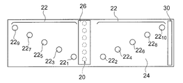
- Sectional drawing which shows the spin wave device by 1st Embodiment. The top view which shows the spin wave device by the 1st modification of 1st Embodiment.
- Sectional drawing which shows the spin wave device by the 2nd modification of 1st Embodiment. The figure which shows an input signal.
- FIGS. 12A to 12C are cross-sectional views showing the magnetization directions of the magnetic layer 18 and the magnetic layer 15.
- the top view which shows one specific example which applied the spin wave device of 2nd Embodiment to the finite impulse response filter.
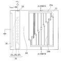
- FIGS. 1 and 2 are a top view and a cross-sectional view, respectively, of the spin wave device 1 of the present embodiment.
- the spin wave device 1 of the present embodiment is provided on the substrate 10, realizes adhesion with the substrate 10 and a good quality thin film, and is provided on the conductive underlayer 12 and the first region of the underlayer 12.
- stacked, and the magnetic layer 18 provided on this multilayer laminated film 13 are provided.
- a set 20 of input electrodes 20 1 to 20 m (m ⁇ 1) arranged in a straight line is provided.
- a set 22 of detection electrodes 22 1 to 22 n (n ⁇ 1) arranged so as to have different distances is provided.
- the distances of the detection electrodes 22 1 to 22 n (n ⁇ 1) from the input electrode set 20 are the distances to the straight line 25 on which the input electrodes 20 1 to 20 m (m ⁇ 1) are arranged.
- dot shape means a circle, an ellipse, a quadrangle, a polygon, and the like.
- the input electrodes 20 1 to 20 m and the detection electrodes 22 1 to 22 n are covered with an insulating layer 24 so that their upper surfaces are exposed.
- the input electrodes 20 1 to 20 m whose upper surfaces are exposed are electrically connected to an input wiring 26 provided on the insulating layer 24, and the detection electrodes 22 1 to 22 n are output wirings 28 provided on the insulating layer 24. Is electrically connected.
- a GND electrode 30 that is electrically connected to the underlayer 12 is provided on the second region of the underlayer 12 where the multilayer laminated film 13 is not provided.
- the GND electrode 30 is provided on the base layer 12, but may be provided on a conductive layer other than the uppermost layer in the multilayer multilayer film 13.
- the input wiring 26 is parallel to the arrangement direction of the input electrodes 20 1 to 20 m , and the width thereof is generated by the current input to the input electrodes 20 1 to 20 m in order to avoid the influence of electromagnetic induction due to the input electric signal. It is desirable to have a length that is at least twice the wavelength of the spin wave.
- the output wiring 28 is preferably configured to match the characteristics of the signal in order to extract the electrical signal output from the detection electrodes 22 1 to 22 n to the outside.
- the detection electrode is arranged only in one region of the input wiring 26, but it is shown in FIG. 3 in order to provide the ease of external connection or suppress the influence of electromagnetic induction of the wiring.
- the detection electrodes 22 1 to 22 10 may be arranged on both sides of the input wiring 26 as in the first modification. That is, the detection electrodes 22 1 , 22 3 , 22 5 , 22 7 , and 22 9 are arranged on the left side of the input wiring 26, and the detection electrodes 22 2 , 22 4 , 22 6 , 22 8 , and 22 10 are placed on the right side of the input wiring 26. You may arrange in. In FIG. 3, for the sake of simplicity, the number of detection electrodes is ten, but the number is not limited to this. In FIG.
- the odd-numbered detection electrodes are arranged on the left side of the input wiring 26 and the even-numbered detection electrodes are arranged on the right side of the input wiring 26.
- the odd-numbered and even-numbered detection electrodes are mixed. It may be arranged on one side and the other side of the input wiring.
- the “maximum diameter” means the long axis when the dot shape is elliptical, and means the maximum length of the diagonal line when the dot shape is rectangular or polygonal.
- the multilayer film structure 13 may be a structure including a magnetic layer.
- You may have a structure.
- the magnetization direction of the magnetic layer 15 is fixed to one direction by the exchange bias effect of the antiferromagnetic layer 14.
- FIG. 5 shows an example of the input signal.
- the input signal is composed of a pulse or impulse signal sequence having a time interval t 0 , and when the spin wave device of the present embodiment is used as a filter, the envelope of the input signal is a signal to be processed.
- the response function H (z) of a finite impulse response filter for a discretized input signal is expressed using a Z-transform form It is expressed as
- Z ⁇ 1 represents a delay of a time interval t 0 of the impulse signal sequence, and the delayed signals are weighted and added to obtain an output signal.
- an infinite number of impulse signal sequences are added.
- a filter is constituted by a finite number (for example, N + 1 (N ⁇ 1)) of impulse signal sequences.
- an input signal I input is input to the input wiring 26 via a capacitor, and this input signal I input is sent to the magnetic layer 18 via the input electrodes 20 1 to 20 m , and spin A wave is induced.
- the induced spin wave propagates through the magnetic layer 18, and an output signal corresponding to the spin wave is extracted from the detection electrodes 22 1 to 22 n .
- An output wiring 28a is connected to the detection electrodes 22 2 to 22 n ⁇ 1 , and a positive output signal I out + is taken out from the output wiring 28a through a capacitor.
- An output wiring 28b is provided so as to face the output wiring 28a, and a negative output signal I out ⁇ is taken out from the output wiring 28b through a capacitor.
- the detection electrodes 22 1 and 22 n are connected to the output wiring 28b.
- the finite impulse response filter of this example has a sufficient number of input electrodes 20 1 to 20 m so that the generated spin wave can be regarded as a plane wave propagating in a direction orthogonal to the direction in which the input wiring 26 extends.
- the detection electrode 22 1 is the detection electrode closest to the set 20 of the input electrodes 20 1 to 20 m
- the detection electrode 22 n is the detection electrode farthest from the detection electrode 22 n
- the detection electrode 22 between them is in order from the closest to the input electrode set 20.
- A0 is the area of the detection electrode serving as a reference, and is desirably set appropriately so that a change in resistance of the detection electrode and a change in output current can be regarded as a proportional relationship.
- the impulse signal input through the input wiring 26 induces a spin wave in the magnetic layer 18 immediately below the input electrodes 20 1 to 20 m .
- the generated spin wave propagates to the detection electrodes 22 1 to 22 n as an impulse-shaped wave packet.
- the input electric impulse signal string is thus converted into a spin wave impulse signal string.
- a constant voltage bias Vb is applied to the detection electrodes 22 1 to 22 n via the output wiring 28a.
- R 0 is It represents the resistance of the magnetic layer 18 / tunnel junction consisting of a tunnel barrier layer 16 / magnetic layer 15 when the junction area a 0, [Delta]
- R represents the resistance change of the tunnel junction which corresponds to the spin wave.
- This current change ⁇ I i is proportional to the spin wave impulse X (Tn ⁇ t 0 ).
- the detection electrode corresponding to the positive weight function h is connected to I out +, and the electrode corresponding to the negative weight function h is separately connected to the terminal of I out ⁇ .
- the tunnel barrier layer 16 is replaced with a nonmagnetic conductive layer (spacer layer) 17 as shown in FIG.
- the spin wave device of the third modified example with the structure replaced with can also obtain the same effect as the present embodiment.
- the generation of spin waves is achieved by passing a spin-polarized current through the magnetic layer 18. That is, the direct magnetic coupling between the magnetic layer 15 and the magnetic layer 18 is achieved by disposing the tunnel barrier layer 16 or the nonmagnetic conductive layer 17 between the magnetic layer 15 that gives a spin-polarized current and the magnetic layer 18.
- a configuration in which a multilayer laminated film 13A laminated in the order of 14 may be provided.
- This multilayer laminated film 13A has a configuration that also serves as the input electrodes 20 1 to 20 m shown in FIG. 1, and the lamination order is reverse to the multilayer laminated film 13 of the second modification shown in FIG. Yes.
- the multilayer laminated film 13 ⁇ / b> A is surrounded by the insulating layer 24 and the upper surface of the antiferromagnetic layer 14 is connected to the input wiring 26.
- the detection electrode is configured to be connected to the upper surface of the magnetic layer 18.
- the spin wave device of the fifth modification shown in FIG. 9 may be used.
- the spin wave device of the fifth modified example has a configuration using a multilayer laminated film 13B in which the tunnel barrier layer 16 is replaced with a nonmagnetic conductive layer 17 instead of the multilayer laminated film 13A in the fourth modified example shown in FIG. have.
- the detection electrode is configured to be connected to the upper surface of the magnetic layer 18.
- the input electrode side realizes adhesion between the magnetic layer 18 and the substrate 10 and a good quality thin film between the magnetic layer 18 and the substrate 10.
- the underlayer 12 having a thin film and a thin multilayer film excellent in electrical conductivity is disposed.
- the detection electrode side for the purpose of detecting a spin wave through the tunnel magnetoresistive effect or the giant magnetoresistive effect. 4 or 7, the tunnel barrier layer 16 or the nonmagnetic conductive layer 17 provided under the magnetic layer 18 between the magnetic layer 18 and the underlayer 12, and the tunnel barrier layer or the nonmagnetic conductive layer.
- the detection electrode is connected to the upper surface of the magnetic layer 18.
- the spin wave detection using the detection electrode is performed using the tunnel magnetoresistance effect or the giant magnetoresistance effect.
- the spin wave detection is realized by converting the change in the current into a current change by the tunnel magnetoresistance effect or the giant magnetoresistance effect. Therefore, as in the sixth modified example shown in FIG. 10, the detection barrier includes a tunnel barrier layer 16 provided on the magnetic layer 18, a magnetic layer 15 provided on the tunnel barrier layer 16, and the magnetic layer.
- a detection electrode having a multilayer film structure of a seventh modification shown in FIG. 11 in which the tunnel barrier layer 16 is replaced with a nonmagnetic conductive layer 17 may be used.
- a tunnel provided under the magnetic layer 18 between the magnetic layer 18 and the underlayer 12 as shown in FIG. 4 or FIG.
- the input electrode is connected to the upper surface of the magnetic layer 18.
- the input electrode may have the structure shown in FIG. 8, and the detection electrode may have the structure shown in FIG. Further, the input electrode may have the structure shown in FIG. 9, and the detection electrode may have the structure shown in FIG.
- the magnetic layer 18 and the magnetic layer 15 are provided.
- the magnetization direction (magnetization axis) when no external magnetic field is applied is substantially parallel to or substantially perpendicular to the film surface.
- the film surface means the upper surface of the magnetic layer 18 or the magnetic layer 15.
- the magnetic material used in the magnetic layer 18 or the magnetic layer 15 in which the magnetization direction is substantially perpendicular to the film surface include FeVPd, FeCrPd, CoFePt, and the like. That is, the magnetic material includes at least one element selected from the group consisting of iron (Fe), cobalt (Co), nickel (Ni), manganese (Mn), and chromium (Cr), and platinum (Pt). , Palladium (Pd), iridium (Ir), ruthenium (Ru), and an alloy containing at least one element selected from the group consisting of rhodium (Rh) can be used. The characteristics of these alloys can be adjusted by the composition of the magnetic material and heat treatment. Further, an amorphous alloy of a rare earth such as TbFeCo or GdFeCo and a transition metal, or a laminated structure of Co / Pt, Co / Pd, or Co / Ni is also desirable.
- a rare earth such as TbFeCo or
- Examples of magnetic materials whose easy axis (direction of magnetization) is substantially parallel to the film surface include, for example, iron (Fe), cobalt (Co), nickel (Ni), manganese (Mn), and chromium (Cr And a magnetic metal containing at least one element selected from the group consisting of:
- the magnetization directions of the magnetic layer 18 and the magnetic layer 15 may be arranged parallel to the film surface and antiparallel to each other (opposite directions). As shown in FIG. 3, the magnetic layer 18 may be arranged so that the magnetization direction is perpendicular to the film surface. In these cases, since the spin wave propagation characteristics do not depend on the in-plane direction, the degree of freedom of electrode arrangement and the like is increased. Further, as shown in FIG. 12C, when the magnetic layer 15 having perpendicular magnetization is used with respect to the magnetic layer 18 having in-plane magnetization, the rising speed when the spin wave is induced by the current is remarkably increased. This is advantageous for high-speed processing.
- the frequency of the high frequency magnetic field generated from the magnetic layer can be tuned by adjusting the magnetic anisotropy and saturation magnetization.
- the attenuation rate of the spin wave can be lowered by reducing the state density of the Fermi surface as in half metal.
- the material of the tunnel barrier layer aluminum (Al), titanium (Ti), zinc (Zn), zirconium (Zr), tantalum (Ta), cobalt (Co), nickel (Ni), silicon (Si), magnesium ( Examples thereof include oxides, nitrides, fluorides, and oxynitrides containing at least one element selected from the group consisting of Mg) and iron (Fe).
- a semiconductor having a large energy gap such as AlAs, GaN, AlN, ZnSe, or ZnO.
- the thickness of the tunnel barrier layer is set to a value within the range of about 0.2 nm to 2.0 nm in order to obtain a large output signal.
- the nonmagnetic conductive layer include copper (Cu), gold (Au), silver (Ag), aluminum (Al), or these copper (Cu), gold (Au), silver (Ag), and aluminum ( Mention may be made of alloys containing at least one element selected from the group consisting of Al).
- the layer thickness is 1.5 nm or more and 20 nm or less, the magnetic layer 18 and the magnetic layer 15 do not interlaminate, and the spin-polarized state of conduction electrons passes through the nonmagnetic conductive layer 17. There is an advantage that it does not need to be lost.
- a spin wave impulse signal based on an impulse input electric signal is generated in the magnetic layer 18, and a signal input to the detection electrode at different timings propagated through the magnetic layer 18 is an electric signal.
- a high-speed operating element showing a finite impulse response can be realized. Therefore, it is possible to realize a spin wave device that can be integrated into an LSI and has a high degree of freedom in design of frequency characteristics.
- FIG. 1A of the present embodiment in the spin wave device 1 of the first embodiment shown in FIG. 2, the output wiring 28 is provided with two output wirings 28a and 28b so as to sandwich the detection electrode 22 therebetween. It has become.
- the detection of the spin wave using the detection electrode is performed using the tunnel magnetoresistance effect or the giant magnetoresistance effect.
- two output wirings 28a and 28b are provided so as to sandwich the detection electrode 22 connected to the magnetic layer 18, and between the two output wirings 28a and 28b.
- the electromotive force generated by the generated spin Hall effect is defined as output.
- a spatial distribution occurs in the spin polarization rate of conduction electrons in the detection electrode 22 due to a phenomenon called spin pumping.
- the portion of the detection electrode 22 in contact with the magnetic layer 18 has the highest spin polarization, and the spin polarization decreases as the surface of the detection electrode 22 on the side opposite to the magnetic layer 18 is approached.
- This spatial distribution of spin polarization also induces a spatial distribution of electric charge in the detection electrode 22, and by detecting this as a voltage, a spin wave signal can be converted into an electric signal.
- FIG. 14 is an enlarged view of one detection electrode 22 and output wirings 28a and 28b connected thereto, as viewed from above.
- the magnitude of the electromotive force Vout generated between the two output wires 28a and 28b is such that the magnetization of the magnetic layer 18 and the straight line 40 connecting the centers of the two locations connecting the detection electrode 22 and each of the output wires 28a and 28b.
- the angle formed in the plane of the magnetic layer 18 with respect to the direction 42 is ⁇ and the amplitude intensity of the spin wave propagating through the magnetic layer 18 immediately below the detection electrode 22 is A, it depends on the angle ⁇ and the amplitude intensity A. To do. That is, the electromotive force V out is proportional to Asin ⁇ .
- the conversion coefficient from the spin wave signal of each detection electrode 22 to the electrical signal for the spin waves of the same intensity can be changed by the angle ⁇ , and weighting can be realized.
- the conversion coefficient for the i-th detection electrode is expressed as w i .
- the distance between the detection electrodes (the distance between the centers of the detection electrodes) based on the propagation direction of the spin wave is the product of the time interval t 0 of the input signal and the group velocity Vg of the spin wave. It is desirable to arrange so that it becomes a value.
- the portion that generates the spin wave is the same as in the first embodiment, and as shown in FIG. 13, the tunnel barrier layer 16 adjacent to the magnetic layer 18 or the nonmagnetic conductive layer between the magnetic layer 18 and the underlayer 12. 17, a tunnel barrier layer 16 or a nonmagnetic conductive layer 17 and a magnetic layer 15 adjacent to the magnetic layer 15 and an antiferromagnetic layer 14 adjacent to the magnetic layer 15, or an input electrode having a multilayer structure as shown in FIGS. You may take the form which becomes.
- the spin wave impulse signal generated by the same method as in the first embodiment reaches the position of each detection electrode after a delay time corresponding to the distance, and is converted into an electric signal corresponding to the conversion coefficient w i .
- the two output wirings 28a and 28b connected to each detection electrode are connected to output terminals A and B, respectively, and the signals generated from all the detection electrodes 22 are electrically added together and output to the outside. Negative weighting is realized by switching the connection positions of the output wirings connected to the respective output terminals. In order to obtain a large signal with high accuracy, it is desirable that the resistance of each detection electrode is sufficiently larger than the input impedance of the subsequent circuit connected to the output terminal.
- a tunnel barrier layer 23 is provided between the detection electrode 22 and the magnetic layer 18 as shown in FIG. It can also be inserted.
- the thickness of the tunnel barrier layer 23 is set to a value within the range of about 0.2 nm to 2.0 nm, the influence of the ground loop can be minimized while maintaining the effect of spin pumping.
- FIGS. 14 and 15 a rectangular detection electrode is taken as an example.
- the in-plane shape is represented by two rotational symmetry or a circle. It is desirable to have high-order rotational symmetry.
- the spin wave impulse signal is generated in the magnetic layer 18 by the impulse input electric signal, and the signals input to the detection electrodes at different timings that have been propagated are converted into electric signals and combined.
- a high-speed operation element that exhibits a finite impulse response can be realized. Therefore, it is possible to realize a spin wave device that can be integrated into an LSI and has a high degree of freedom in design of frequency characteristics.
- FIGS. 4 and 6 ten input electrodes 20 1 to 20 10 that pass through the insulating layer 24 and are adjacent to the magnetic layer 18, and similarly pass through the insulating layer 24 and pass through the magnetic layer 18.
- the diameter of each of the input electrodes 20 1 to 20 10 is 50 nm.
- Detection electrodes 22 5 intermediate is a detecting electrode as a reference, a diameter of 100 nm.
- cut-off angular frequency ⁇ c 2 ⁇ f c
- the sampling period T 1 / f s.
- the finite impulse response low frequency transmission filter of this example has a laminated structure shown in FIG. CoFeB was used as the magnetic layer 18, MgO was used as the tunnel barrier layer 16, and CoFe / CoFeB was used as the magnetic layer 15. Magnetization of the magnetic layer 15 is pinned by the antiferromagnetic layer 14 made of IrMn from the left to the right of the drawing. On the other hand, the magnetization of the magnetic layer 18 is antiparallel to the magnetization of the magnetic layer 15 in the absence of an external magnetic field.
- the finite impulse response filter of this example is manufactured as follows. First, after forming the base layer 12 on the wafer (substrate) 10, the wafer 10 is placed in an ultra-high vacuum sputtering apparatus. Next, on the underlayer 12, an antiferromagnetic layer 14 made of IrMn, a magnetic layer 15 made of CoFe / CoFeB, a tunnel barrier layer 16 made of MgO, a magnetic layer 18 made of CoFeB, and a cap layer made of Ru (FIG. (Not shown) are stacked in this order. Then, the magnetization of the magnetic layer 15 made of CoFe / CoFeB was fixed by annealing in a magnetic field. Further, a magnetic field is applied at room temperature to fix the magnetization of the magnetic layer 18 made of CoFeB in antiparallel to the magnetization direction of the magnetic layer 15 made of CoFe / CoFeB.
- a resist is applied to the entire surface, and this resist is patterned by a stepper exposure apparatus using KrF, and an opening is formed in the resist at a position corresponding to the GND electrode 30. Then, using the resist in which the opening is formed as a mask, using an ion milling method, the antiferromagnetic layer 14, the magnetic layer 15, the tunnel barrier layer 16, the magnetic layer 18 on the region where the GND electrode 30 is formed, and A cap layer (not shown) made of Ru is scraped off to expose the upper surface of the base layer 12.
- an EB (electron beam) resist is applied on the cap layer and EB exposure is performed, and openings corresponding to the GND electrode 30, the input electrodes 20 1 to 20 10 , and the detection electrodes 22 1 to 22 9 are performed. Is formed on the EB resist. Then, openings corresponding to the GND electrode 30, the input electrodes 20 1 to 20 10 , and the detection electrodes 22 1 to 22 9 are filled with Cu, and the EB resist is removed to remove the GND electrode 30 and the input electrodes 20 1. To 20 10 and detection electrodes 22 1 to 22 9 are formed.
- a multilayer structure comprising the antiferromagnetic layer 14 / magnetic layer 15 / tunnel barrier layer 16 / magnetic layer 18, the GND electrode 30, the input electrodes 20 1 to 20 10 , and the detection electrodes 22 1 to 22 9 are completely formed.
- a SiO 2 layer 24 is formed so as to cover it. Thereafter, the surfaces of the SiO 2 layer 24 are planarized by ion milling to expose the upper surfaces of the GND electrode 30, the input electrodes 20 1 to 20 10 , and the detection electrodes 22 1 to 22 9 .
- the input wiring 26 and the output wiring 28 connected to the input electrodes 20 1 to 20 10 and the detection electrodes 22 1 to 22 9 are formed.
- the input wiring 26 and the output wiring 28 are formed by applying a resist on the entire surface, patterning the resist using a KrF stepper exposure apparatus, and inputting the input electrodes 20 1 to 20 10 and the detection electrodes 22 1 to 22 9 in the resist. Openings are formed to connect to the two. Then, after the opening is filled with Cu, the resist is removed and formed.
- a pulsed current having a half width of 200 ps is passed through the input electrode in advance, and the center frequency of the propagating spin wave is detected by performing time-resolved detection with a signal detection electrode having a different distance from the signal analysis by the spectrum analyzer connected to the input electrode.
- a signal detection electrode having a different distance from the signal analysis by the spectrum analyzer connected to the input electrode was about 12.4 GHz and the group velocity was 0.98 ⁇ m / nsec.
- a constant bias voltage is applied to each of the input electrodes 20 1 to 20 10 and the detection electrodes 22 1 to 22 9 , and an impulse train including a repetition frequency of 3.3 GHz and a half-value width of 200 ps is converted into a sine wave sin ( ⁇ t).
- the amplitude-modulated signal is input to the input electrode through the capacitance couple and the frequency of the sine wave is swept from 500 MHz to 1.5 GHz, the same sine-wave modulated impulse signal as the input signal having an amplitude of 10 ⁇ A is obtained from the output terminal up to 1 GHz
- the frequency exceeded 1 GHz the amplitude suddenly decreased, and it was confirmed that the finite impulse response low frequency transmission filter of this example was operating as designed.
- a 200 Oe magnetic field is applied in a direction parallel to the magnetization direction of the magnetic layer 18 from the bottom to the top toward the paper surface to set the spin wave group velocity to 0.75 ⁇ m / nsec, and the impulse train is repeated.
- a cutoff frequency of 750 MHz could be obtained and that the filter characteristics could be tuned by the applied magnetic field.
- the present embodiment is a finite impulse response low frequency transmission filter in which an input electrode and a detection electrode have a multilayer structure.
- the size, arrangement, and number of the on / off detection electrodes are the same as in the first embodiment.
- the finite impulse response low frequency band transmission filter of the second embodiment is manufactured as follows. First, after forming the base layer 12 on the wafer (substrate) 10, the wafer 10 is placed in an ultra-high vacuum sputtering apparatus. Subsequently, a magnetic layer 18 made of CoFeB, a tunnel barrier layer 16 made of MgO, a magnetic layer 15 having a CoFeB / CoFe laminated structure, an antiferromagnetic layer 14 made of IrMn, and a cap layer made of Ru are formed on the underlayer 12. (Not shown) are deposited in this order. Then, the magnetization of the magnetic layer 15 made of CoFe / CoFeB is fixed by annealing in a magnetic field. Thereafter, a magnetic field was applied at room temperature to fix the magnetization of the magnetic layer 18 so that the magnetization directions of the magnetic layer 15 and the magnetic layer 18 made of CoFeB were antiparallel to each other.
- a resist is applied to the entire surface, and the resist is patterned by a stepper exposure apparatus using KrF, and an opening is formed in a region where the GND electrode 30 is formed in the resist. Subsequently, using the resist in which the opening is formed as a mask, the magnetic layer 18, the tunnel barrier layer 16, the magnetic layer 15, and the cap layer on the region where the GND electrode 30 is to be formed are scraped off by ion milling. Then, the upper surface of the base layer 12 is exposed.
- an EB resist is applied again on the entire surface, and patterning is performed using EB exposure so that only the portions of the GND electrode 30, the input electrode 20, and the detection electrode 30 remain. Then, using the patterned resist as a mask, the magnetic layer 15, the antiferromagnetic layer 14, and the cap layer are scraped off using an ion milling method until the upper surface of the tunnel barrier layer 16 is exposed in a portion where the resist does not remain.
- an insulating layer 24 made of SiO 2 with the patterned resist as it is is deposited on the exposed portion of the upper surface of the tunnel barrier layer 16 using a sputtering apparatus, and the input electrode that has not been cut by ion milling and The detection electrode is embedded in the insulating layer 24. Then, the resist is peeled off together with the SiO 2 layer formed thereon.
- a resist is applied again on the entire surface, and a resist pattern having openings corresponding to the wiring of the input wiring 26, the output wiring 28, and the GND electrode 30 is formed using a stepper exposure apparatus using KrF. Then, Cu is embedded in the opening to form a film, and the resist is removed to form the input wiring 26, the output wiring 28, and the GND wiring.
- the finite impulse response low-frequency transmission filter manufactured in this way exhibits substantially the same frequency characteristics as the finite impulse response low-frequency transmission filter of the first embodiment, while applying the same signal voltage to the input electrode. However, only a current of 3 ⁇ A flowed.
- the finite impulse response low frequency transmission filter of the present embodiment requires more manufacturing steps than the first embodiment, but the current confinement can be performed efficiently, so the finite impulse response low frequency with low power consumption. It becomes a band transmission type filter.
- the present embodiment is a finite impulse response low frequency transmission filter using spin pumping and the spin Hall effect as a method of detecting the spin wave of the detection electrode.
- the present embodiment is a finite impulse response low frequency transmission filter using spin pumping and the spin Hall effect as a method of detecting the spin wave of the detection electrode.
- the laminated structure and the magnetization directions of the magnetic layer 18 and the magnetic layer 15 are the same as in the first embodiment.
- the finite impulse response low frequency band transmission filter of the third embodiment is manufactured as follows. First, after forming the base layer 12 on the wafer (substrate) 10, the wafer 10 is placed in an ultra-high vacuum sputtering apparatus. Subsequently, on the underlayer 12, an antiferromagnetic layer 14 made of IrMn, a magnetic layer 15 having a laminated structure of CoFe / CoFeB, a tunnel barrier layer 16 made of MgO, a magnetic layer 18 made of CoFeB, and a cap made of Ru. Layers (not shown) are stacked in this order. Then, the magnetization of the magnetic layer 15 made of CoFe / CoFeB is fixed from the left to the right in FIG. 13, for example, by annealing in a magnetic field. Further, a magnetic field is applied at room temperature to fix the magnetization of the magnetic layer 18 made of CoFeB in antiparallel to the magnetization direction of the magnetic layer 15.
- a resist is applied to the entire surface, and this resist is patterned by a stepper exposure apparatus using KrF, thereby forming an opening at a position corresponding to the GND electrode in the resist.
- the antiferromagnetic layer 14 using an ion milling method, the antiferromagnetic layer 14, the magnetic layer 15, the tunnel barrier layer 16, the magnetic layer 18 on the region where the GND electrode 30 is formed, and The cap layer is scraped off to expose the upper surface of the foundation layer 12.
- an EB resist is applied on the cap layer and EB exposure is performed to form an opening in a region of the EB resist where the GND electrode and the input electrode are formed. Then, an opening corresponding to a region where the GND electrode and the input electrode are formed is filled with Cu, and the EB resist is removed to form the GND electrode and the input electrode.
- EB resist is applied again and EB exposure is performed to form an opening corresponding to the detection electrode in the EB resist. Then, the film corresponding to the detection electrode is filled with Pt having a large spin orbit interaction, and the detection electrode is formed by removing the EB resist.
- the SiO 2 layer 24 is formed so as to completely cover the antiferromagnetic layer 14 / magnetic layer 15 / tunnel barrier layer 16 / magnetic layer 18 multilayer structure, GND electrode, input electrode, and detection electrode. Thereafter, the upper surface of the GND electrode, the input electrode, and the detection electrode is exposed by planarizing the surface of the SiO 2 layer 24 using an ion milling method.
- an input wiring and an output wiring connected to each of the input electrode and the detection electrode are formed.
- a resist is applied to the entire surface, and this resist is patterned by a stepper exposure apparatus using KrF to form openings connected to the input electrode and the detection electrode in the resist. Then, after the opening is filled with Cu, the resist is removed and formed.
- the thus produced finite impulse response low frequency band transmission type filter showed substantially the same frequency characteristics as the finite impulse response low frequency band transmission type filter of the first embodiment. Further, although the output signal intensity is as small as about 20% of the first embodiment, it is not necessary to connect a power source from the outside to the detection electrode, and a low power consumption finite impulse response low frequency transmission filter can be realized. It was.
- a spin wave device that can be integrated into an LSI and has a high degree of freedom in design of frequency characteristics can be realized.
Landscapes
- Physics & Mathematics (AREA)
- Electromagnetism (AREA)
- Hall/Mr Elements (AREA)
- Control Of Motors That Do Not Use Commutators (AREA)
- Waveguide Switches, Polarizers, And Phase Shifters (AREA)
- Waveguides (AREA)
Abstract
LSIに集積化が可能でかつ周波数特性の設計自由度の高いスピン波デバイスを実現することを可能にする。スピン波デバイスは、入力インパルス信号を伝える1本の入力配線と、下地層を含む多層膜と、前記多層膜上に設けられ前記入力インパルス信号を受けることによりスピン波を発生し、前スピン波を伝搬する第1の磁性層と、前記第1の磁性層上に一直線上に配列されるとともに前記入力配線に接続され、前記入力インパルス信号を前記第1の磁性層に伝える複数の入力電極と、前記第1の磁性層中を伝搬した前記スピン波を検出する複数の検出電極であって、前記複数の入力電極が配列された前記直線からの距離が異なるようにそれぞれが前記第1の磁性層上に設けられた複数の検出電極と、を備え、検出電極の個数をn(n≧2)とし、第i(n≧i≧1)番目の検出電極の直線からの距離をLiとし、スピン波の群速度をVgとし、前記入力インパルス信号のパルス周期をt0とすると、隣接する第i(n-1≧i≧1)番目の検出電極と第i+1番目の検出電極と間の直線に直交する方向における距離dは、d=Vg×t0と表される。
Description
本発明は、スピン波デバイスに関する。
高周波電気信号用のフィルタがスピン波の一種である静磁波を用いて実現されている(例えば、非特許文献1参照)、この非特許文献1に記載されている静磁波フィルタは、ガドリニウムガリウムガーネット基板(以下、GGG基板とも云う)上にエピタキシャル成長されたイットリウム鉄ガーネット薄膜(以下、YIG薄膜とも云う)と、下部全面に電気的接地電極を有し上面に2つの金属細線トランデューサを有する誘電体基板と、を備えている。静磁波フィルタ内ではYIG薄膜の表面と、誘電体基板上のトランデューサは互いに接するように配置される。
入力トランデューサに入力された高周波電気信号はその周り(近傍)に高周波磁界を発生させる。入力トランデューサの近傍に発生した高周波磁界はYIG薄膜の一部に磁気モーメントの歳差運動を誘起する。誘起された歳差運動はスピン波としてYIG薄膜内を出力トランデューサまで伝搬する。出力トランデューサまで伝搬されたスピン波は入力とは反対の過程によって出力トランデューサ内に高周波電気信号を誘起する。その結果、この静磁波フィルタは、入力トランデューサで励起されかつ出力トランデューサで検出できるスピン波の周波数帯域にある電気信号を透過する帯域制限フィルタとして動作する。
また、非特許文献2には、複数の電極から構成される出力トランデューサを用いた静磁波フィルタが報告されている。入力トランデューサからの距離が異なる位置に入検出電極を配置し、電極の長さとその内部を流れる電流の向きによってスピン波信号の重ね合わせの制御と、検出信号の重み付けとを行うことで所望の周波数特性を持つフィルタを作ることができる。
"Magnetostatic waves and their applications"by P. Kabos and V. S. Stalmachov (Chapman & Hall, 1994, London).
Y. J. Ataiiyan et. al., "MSSW transversal filters on current weighting in narrow (10μm) Transducers", IEEE MTT-S Digest, 576 (1986).
しかしながら、これらのフィルタは集積化の点で問題があった。発生させる静磁波の波長はトランデューサの電極の幅に依存しており、1μm程度の幅では短波長で伝搬速度の速い交換スピン波が励起されるので小型化が難しい。加えて静磁波フィルタに用いるスピン波伝搬媒体にはスピン歳差運動が緩和し難い特性が要求され、これまでYIG薄膜が最もよく用いられてきた。この材料は、混載などの方法によってLSI(大規模集積回路)と、静磁波フィルタとを集積化することに対して非常に大きな障壁となっている。YIG薄膜はGGG結晶基板の上にエピタキシャル成長によって成膜される結晶性薄膜である。そして、特定の結晶基板へのエピタキシャル成長を通常のLSIの作製プロセスで実現することができず、事実上静磁波フィルタのLSIへの集積化は不可能な状況にある。
また、静磁波フィルタには、特性面においても課題が存在する。トランデューサの動作原理より、フィルタで処理する信号の周波数とスピン波の周波数とが同じになるため、YIG薄膜中の静磁波の伝搬特性がフィルタの特性に直接反映される。このことはフィルタの設計に大きな制限を与える。例えば、帯域制限フィルタを設計する場合、遮断周波数は高周波側ではトランデューサの静磁波励起および検出帯域によって、低周波数側は静磁波の周波数帯域幅によってそれぞれ制限される。特に後者は材料に依存するため、YIG薄膜または類似する材料を用いる限り、低周波数側へ帯域を伸ばすことが困難であった。
本発明は、上記事情を考慮してなされたものであって、LSIに集積可能でかつ周波数特性の設計自由度が高いスピン波デバイスを提供することを目的とする。
本発明の第1の態様によるスピン波デバイスは、入力インパルス信号を伝える1本の入力配線と、下地層を含む多層膜と、前記多層膜上に設けられ前記入力インパルス信号を受けることによりスピン波を発生し、前スピン波を伝搬する第1の磁性層と、前記第1の磁性層上に一直線上に配列されるとともに前記入力配線に接続され、前記入力インパルス信号を前記第1の磁性層に伝える複数の入力電極と、前記第1の磁性層中を伝搬した前記スピン波を検出する複数の検出電極であって、前記複数の入力電極が配列された前記直線からの距離が異なるようにそれぞれが前記第1の磁性層上に設けられた複数の検出電極と、を備え、前記検出電極の個数をn(n≧2)とし、第i(n≧i≧1)番目の検出電極の前記直線からの距離をLiとし、前記スピン波の群速度をVgとし、前記入力インパルス信号のパルス周期をt0とすると、隣接する第i(n-1≧i≧1)番目の検出電極と第i+1番目の検出電極と間の前記直線に直交する方向における距離dは、d=Vg×t0と表されることを特徴とする。
本発明によれば、LSIに集積化が可能でかつ周波数特性の設計自由度の高いスピン波デバイスを提供することができる。
本発明の実施形態を以下に図面を参照して説明する。
(第1実施形態)
本発明の第1実施形態によるスピン波デバイスを図1および図2に示す。図1および図2はそれぞれ、本実施形態のスピン波デバイス1の上面図および断面図である。
本発明の第1実施形態によるスピン波デバイスを図1および図2に示す。図1および図2はそれぞれ、本実施形態のスピン波デバイス1の上面図および断面図である。
本実施形態のスピン波デバイス1は基板10上に設けられていて、基板10との密着性および良質な薄膜を実現しかつ導電性の下地層12と、下地層12の第1の領域上に設けられた少なくとも2層の薄膜が積層された多層積層膜13と、この多層積層膜13上に設けられた磁性層18と、を備えている。この磁性層18上には、図1に示すように、一直線状に配列された入力電極201~20m(m≧1)の組20が設けられているとともに、入力電極の組20からの距離がそれぞれ異なるように配列された検出電極221~22n(n≧1)の組22が設けられている。ここで、検出電極221~22n(n≧1)の、入力電極の組20からの距離とはそれぞれ、入力電極201~20m(m≧1)が配列された直線25までの距離Li、すなわち各検出電極22i(i=1,・・・,n)の中心から上記直線25への垂線の長さLiを意味する。各入力電極20i(i=1,・・・,m)および各検出電極22j(j=1,・・・,n)はそれぞれ、ドット形状の接触面を有し、この接触面を介して磁性層18と接続する。各入力電極20i(i=1,・・・,m)および各検出電極22j(j=1,・・・,n)と、磁性層18と直接に接触しても構わないし、導電層(後述のキャップ層)を介して接触してしてもよい。なお、本明細書では、「ドット形状」とは、円形、楕円形、四角形、多角形等を意味する。
これらの入力電極201~20mおよび検出電極221~22nはそれぞれの上面が露出するように絶縁層24に覆われている。上面が露出された入力電極201~20mは絶縁層24上に設けられた入力配線26に電気的に接続され、検出電極221~22nは絶縁層24上に設けられた出力配線28に電気的に接続される。また、多層積層膜13が設けられていない下地層12の第2の領域上に、下地層12と電気的に接続するGND電極30が設けられている。なお、本実施形態においては、GND電極30は、下地層12上に設けられたが、積層多層膜13のうちの、最上層を除くある導電性の層上に設けてもよい。
入力配線26は入力電極201~20mの配列方向と並行で、その幅は、入力電気信号による電磁誘導の影響を避けるため、入力電極201~20mに入力された電流によって生成されるスピン波の波長の少なくとも2倍の長さを有するように構成することが望ましい。
また、出力配線28は、検出電極221~22nから出力される電気信号を外部へ取り出すため信号の特性に合わせるように構成されることが望ましい。
なお、本実施形態においては、検出電極は、入力配線26の片側の領域にのみ配置されていたが、外部接続の容易さを提供するまたは配線の電磁誘導の影響を抑えるために図3に示す第1変形例のように、検出電極221~2210を入力配線26の両側に配置してもよい。すなわち、検出電極221、223、225、227、229を入力配線26の左側に配置し、検出電極222、224、226、228、2210を入力配線26の右側に配置してもよい。なお、図3においては、説明を簡単にするために、検出電極は10個であったが、この個数に限定されるものではない。また、図3においては、奇数番目の検出電極を入力配線26の左側に配置し、偶数番目の検出電極を入力配線26の右側に配置したが、奇数番目と偶数番目の検出電極を混在して入力配線の一方の側と他方の側に配置してもよい。
また、入力電極の組20からGND電極30に通電する。すなわち各入力電極20i(i=1,・・・,m)の接触面に略垂直の方向に電圧を印加するか、もしくは電流を流す。これにより引き起こされるスピントルクによって、各入力電極20i(i=1,・・・,m)の接触面下の磁性層18の領域にスピン波が励起され、磁性層18中を伝搬する。磁性層18中を伝搬するスピン波に応じた電気信号が検出電極221~22nから取り出される。だだし、各入力電極20i(i=1,・・・,m)および各検出電極22j(j=1,・・・,n)におけるドット形状の接触面の最大直径が500nmを超えて大きい場合には、複雑な多磁区の磁化構造が、各入力電極20i(i=1,・・・,m)および各検出電極22j(j=1,・・・,n)に励起されるため、スピン波制御が困難となり望ましくない。ここで、「最大直径」とは、ドット形状が楕円形の場合は長軸を意味し、四角形または多角形の場合は対角線の最大長さを意味する。
なお、磁性層18中を伝搬するスピン波に応じた電気信号を取り出すために、多層膜構造13は、磁性層を含む構造であってもよい。例えば、図4に示す第2変形例のように、下地層12と磁性層18との間に、反強磁性層14、磁性層15、およびトンネルバリア層(スペーサ層)16が積層された積層構造を有していてもよい。磁性層15の磁化の方向は反強磁性層14の交換バイアス効果によって磁化の方向が一方向に固定されている。
入力電極の組20とGND電極30との間に通電すると、磁性層15より磁性層18へスピン偏極した電子が注入され、スピントルクが磁性層18の磁化に与えられることで、スピン波が発生する。発生したスピン波は磁性層18中を伝搬して検出電極の組22の直下まで到達する。この際、検出電極の組22とGND電極30との間に定電圧電源を用いて定電圧を印加しておくと、スピン波による磁性層18の磁化の歳差運動によって検出電極の組22の直下における、磁性層18/トンネルバリア層16/磁性層15からなるトンネル接合の抵抗が変化して、通電電流に変化が生じる。抵抗変化はスピン波の振幅強度におおよそ比例するため、スピン波の強度を電気信号に変換することができる。
本実施形態においては、入力配線26を介して各入力電極20i(i=1,・・・,m)に入力される入力信号としては、時間的に離散化された電気信号を想定している。図5に入力信号の一例を示す。入力信号は時間間隔t0のパルスもしくはインパルス信号列から構成され、フィルタとして本実施形態のスピン波デバイスを用いる場合には、入力信号の包絡線が処理を行う対象の信号となる。
一般に、離散化入力信号に対する有限インパルス応答フィルタの応答関数H(z)はZ変換形式を用いて

と表わされる。ここで、重み関数列h(k)(k=0,1,・・・)を適切に選ぶことで、任意の周波数応答を持ったパッシブなフィルタを実現できる。Z-1はインパルス信号列の時間間隔t0分の遅延を表しており、遅延させた信号に重み付けを行い合算して出力信号とする。上記(1)式においては、無限個のインパルス信号列を加算していたが、現実の系においては有限個(例えば、N+1個(N≧1))のインパルス信号列によってフィルタを構成する。
次に、本実施形態のスピン波デバイス1を有限インパルス応答フィルタに適用した例を図6に示す。この例の有限インパルス応答フィルタにおいては、入力配線26にはコンデンサを介して入力信号Iinputが入力され、この入力信号Iinputは入力電極201~20mを介して磁性層18送られ、スピン波が誘起される。この誘起されたスピン波は磁性層18中を伝搬し、このスピン波に応じた出力信号が検出電極221~22nから取り出される。検出電極222~22n-1には出力配線28aが接続され、この出力配線28aからコンデンサを介して正側の出力信号Iout+が取り出される。また、出力配線28aに対向するように出力配線28bが設けられ、この出力配線28bからコンデンサを介して負側の出力信号Iout-が取り出される。なお、図6においては、出力配線28bには検出電極221、22nが接続されている。
この例の有限インパルス応答フィルタは、生成するスピン波が入力配線26の延在する方向と直交する方向に伝搬する平面波と見なせるように、十分な数の入力電極201~20mを有している。スピン波の伝搬方向における、隣接する検出電極22i、22i+1(i=1,・・・,n-1)間の距離(入力配線26に直交する方向における検出電極間の中心間距離)dは入力信号の時間間隔t0とスピン波の群速度Vgとの積になるように配置されることが望ましい。
磁場、電場、光などの外場を磁性層18に与えてその磁気特性を変調すると群速度も変化する。変調後の群速度をVg’とすると、本例の有限インパルス応答フィルタは、時間間隔t0’(=d/Vg’)の信号に対して元の周波数特性とは異なる特性を持ったフィルタとして動作させることもできる。入力電極201~20mの組20に最も近い検出電極を検出電極221、最も遠い検出電極を検出電極22nとし、その間の検出電極を入力電極の組20に近い方から順に検出電極22i(i=1,・・・,1)とし、その面積をAi=A0×h(i)とする。ここでA0は基準となる検出電極の面積で、検出電極の抵抗変化と出力電流の変化が比例関係とみなせるように適切に設定されることが望ましい。
入力配線26を通して入力されたインパルス信号は入力電極201~20mの直下の磁性層18にスピン波を誘起する。生成されたスピン波はインパルス形状の波束となって検出電極221~22nへ伝搬していく。入力された電気インパルス信号列はこのようにしてスピン波のインパルス信号列に変換される。検出電極221~22nには出力配線28a介して定電圧バイアスVbが印加されている。ある時刻Tにおいて入力電極201~20mによって生成されたスピン波インパルスX(T)が検出電極221に到達したとき、各検出電極22i(i=1,・・・,n)において流れる電流に、スピン波に対応する電流変化ΔIiが生じる。この電流変化ΔIiは次の(2)式で表される。

ここで、h(k)(k=0,1,・・・)は(1)式で示した重み関数列h(k)(k=0,1,・・・)を表し、R0は接合面積A0のときの磁性層18/トンネルバリア層16/磁性層15からなるトンネル接合の抵抗を表し、ΔRはスピン波に対応する上記トンネル接合の抵抗変化を表す。この電流変化ΔIiはスピン波インパルスX(T-n×t0)に比例している。正の重み関数hに対応する検出電極はIout+に接続され、負の重み関数hに対応する電極はIout-の端子に別々に接続されている。これら二つの出力信号は、図示しない外部の差動増幅回路に接続され、その差(=Iout+-Iout-)の形で出力される。
なお、周辺回路との電気的特性の整合性を考え、図4に示す第2変形例のスピン波デバイスにおいて、トンネルバリア層16を、図7に示すように非磁性導電層(スペーサ層)17に置き換えた構造の第3変形例のスピン波デバイスも、本実施形態と同様の効果を得ることができる。
トンネルバリア層16を用いた第2変形例の場合と同様に入力電極とGND電極との間にインパルス電気信号を印加することでスピン波インパルス信号を生成することが可能である。また出力に関しても図6で説明した形態にすることによって、巨大磁気抵抗効果(GMR)を介してスピン波を検出し、所望の信号を出力することができる。
本実施形態またはその変形例においては、スピン波の生成はスピン偏極した電流を磁性層18に通電することで達成される。つまり、スピン偏極した電流を与える磁性層15と、磁性層18との間にトンネルバリア層16もしくは非磁性導電層17を配置することにより、磁性層15と磁性層18との直接的磁気結合を防止しつつスピン偏極した電流を磁性層18へ導入することが本実施形態またはその変形例において肝要である。したがって、図8に示す第4変形例のスピン波デバイスのように、下地層12上に磁性層18を設け、この磁性層18上に、トンネルバリア層16、磁性層15、および反強磁性層14の順序で積層された多層積層膜13Aが設けられた構成としてもよい。この多層積層膜13Aは、図1に示す入力電極201~20mを兼用した構成となっており、積層順序が図4に示す第2変形例の多層積層膜13と逆の順序となっている。そして、多層積層膜13Aは、側面が絶縁層24によって取り囲まれ、反強磁性層14の上面が入力配線26と接続する。この第4変形例においては、検出電極は、磁性層18の上面に接続する構成となっている。
また、図9に示す第5変形例のスピン波デバイスであってもよい。この第5変形例のスピン波デバイスは、図8に示す第4変形例において、多層積層膜13Aの代わりに、トンネルバリア層16を非磁性導電層17に置き換えた多層積層膜13Bを用いた構成を有している。この第5変形例においても、検出電極は、磁性層18の上面に接続する構成となっている。
なお、図8および図9で示した第4および第5変形例においては、入力電極側は、磁性層18と基板10との間に、基板10との密着性と良質な薄膜を実現するための薄膜と電気伝導性に優れた薄膜の多層膜を有する下地層12のみが配置されているが、検出電極側において、トンネル磁気抵抗効果もしくは巨大磁気抵抗効果を介してスピン波を検出する目的で、図4または図7に示すように、磁性層18と下地層12との間に、磁性層18下に設けられたトンネルバリア層16もしくは非磁性導電層17と、トンネルバリア層もしくは非磁性導電層下に設けられた磁性層15と、この磁性層15下に設けられた反強磁性層との積層構造を有するように配置してもよい。すなわち、検出電極側においては、下地層12、反強磁性層14、磁性層15、トンネルバリア層16もしくは非磁性導電層17、および磁性層18の順に積層される。したがって、この場合、検出電極は、磁性層18の上面と接続する。
また、第1実施形態においては、検出電極を用いたスピン波検出をトンネル磁気抵抗効果もしくは巨大磁気抵抗効果を利用して行う。磁性層18と磁性層15との間にトンネルバリア層16もしくは非磁性導電層17を配置して両層の直接的磁気結合を抑制しつつ、磁性層15の磁化に対する磁性層18の磁化の方向の変化をトンネル磁気抵抗効果もしくは巨大磁気抵抗効果によって電流変化に変換することでスピン波検出が実現される。したがって、図10に示す第6変形例のように、検出電極が、磁性層18上に設けられたトンネルバリア層16と、このトンネルバリア層16上に設けられた磁性層15と、この磁性層15上に設けられ磁性層15の磁化方向を一方向に固定する反強磁性層14とを有する多層膜構造を有していてもよい。また、トンネルバリア層16を非磁性導電層17に置き換えた、図11に示す第7変形例の多層膜構造を有した検出電極としてもよい。なお、これらの場合において、入力電極側においてスピン波を生成する目的で、図4または図7に示すように、磁性層18と下地層12との間に、磁性層18下に設けられたトンネルバリア層16もしくは非磁性導電層17と、トンネルバリア層16もしくは非磁性導電層17下に設けられた磁性層15と、この磁性層15下に設けられた反強磁性層14との積層構造を有するように配置してもよい。すなわち、検出電極側においては、下地層12、反強磁性層14、磁性層15、トンネルバリア層16もしくは非磁性導電層17、および磁性層18の順に積層される。したがって、この場合、入力電極は、磁性層18の上面と接続する。
また、入力電極として図8に示す構造を有し、検出電極として図10に示す構造を有するように構成してもよい。また、入力電極として図9に示す構造を有し、検出電極として図11に示す構造を有するように構成してもよい。
本実施形態およびその変形例においては、磁性層18と磁性層15とを備えている。これらの磁性層18および磁性層15における、外部磁界が印加されていない場合の磁化の方向(磁化容易軸)は、膜面に略平行かまたは略垂直となっている。ここで、膜面とは、磁性層18または磁性層15の上面を意味する。
これらの磁性層18または磁性層15に用いられる、磁化の向きが膜面に対して略垂直方向となる磁性材料としては、FeVPd、FeCrPd、CoFePt等が挙げられる。すなわち、上記磁性材料としては、鉄(Fe)、コバルト(Co)、ニッケル(Ni)、マンガン(Mn)、およびクロム(Cr)よりなる群から選択された少なくとも一つの元素と、白金(Pt)、パラジウム(Pd)、イリジウム(Ir)、ルテニウム(Ru)、ロジウム(Rh)よりなる群から選択された少なくとも一つの元素と、を含む合金を用いることができる。これらの合金は、磁性材料の組成や熱処理により特性を調整することができる。また、TbFeCo、GdFeCoなどの希土類と遷移金属とのアモルファス合金、またはCo/Pt、Co/Pd、Co/Niの積層構造なども望ましい。
また、磁化容易軸(磁化の方向)が膜面に対して略平行となる磁性材料としては、例えば、鉄(Fe)、コバルト(Co)、ニッケル(Ni)、マンガン(Mn)、クロム(Cr)よりなる群から選択された少なくとも一つの元素を含む磁性金属が挙げられる。
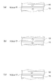
磁性層18および磁性層15の磁化の向きは図12(a)に示すように、膜面に平行でかつ互いに反平行(逆の向き)となっている配置でもよいし、図12(b)に示すように磁性層18の磁化の向きが膜面に垂直となる配置であってもよい。これらの場合、スピン波伝搬特性に面内方向依存性がないので電極の配置などの自由度が広がる。また、図12(c)に示すように、面内磁化を有する磁性層18に対して垂直磁化を有する磁性層15を用いると、電流によってスピン波を誘起する際の立ち上がり速度が著しく速くなり、高速処理を行う上で有利である。
以上の磁性体を磁性層に用いる場合、磁気異方性と飽和磁化を調整することで磁性層から発生する高周波磁場の周波数をチューニングすることができる。また、ハーフメタルのようにフェルミ面の状態密度を小さくすることでスピン波の減衰率を下げることができる。
トンネルバリア層の材料としては、アルミニウム(Al)、チタン(Ti)、亜鉛(Zn)、ジルコニウム(Zr)、タンタル(Ta)、コバルト(Co)、ニッケル(Ni)、シリコン(Si)、マグネシウム(Mg)、鉄(Fe)よりなる群から選択された少なくとも一つの元素を含む酸化物、窒化物、フッ化物、酸窒化物などが挙げられる。あるいは、AlAs、GaN、AlN、ZnSe、ZnOなどの大きなエネルギーギャップを有する半導体を有することが好ましい。また、トンネルバリア層の厚さを約0.2nm~2.0nm程度の範囲内の値とすることが、大きな出力信号を得るに当たっては好ましい。
非磁性導電層の具体的材料としては、銅(Cu)、金(Au)、銀(Ag)、アルミニウム(Al)、またはこれら銅(Cu)、金(Au)、銀(Ag)、アルミニウム(Al)よりなる群から選択された少なくとも一つの元素を含む合金を挙げることができる。この場合の層厚は1.5nm以上、20nm以下であると、磁性層18と磁性層15とが層間結合せず、かつ、伝導電子のスピン偏極状態は非磁性導電層17を通過する際に失わせないで済むという利点がある。
以上説明したように、本実施形態によれば、磁性層18にインパルス入力電気信号によるスピン波インパルス信号を発生させ、磁性層18を伝搬してきた異なるタイミングで検出電極に入力される信号を電気信号に変換し合算することで、有限インパルス応答を示す高速動作素子を実現することができる。したがって、LSIに集積化が可能でかつ周波数特性の設計自由度の高いスピン波デバイスを実現することができる。
(第2実施形態)
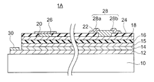
次に、本発明の第2実施形態によるスピン波デバイスを図13に示す。本実施形態のスピン波デバイス1Aは、図2に示す第1実施形態のスピン波デバイス1において、出力配線28として、検出電極22を挟むように、2個の出力配線28a、28bを設けた構成となっている。第1実施形態においては、検出電極を用いたスピン波の検出はトンネル磁気抵抗効果もしくは巨大磁気抵抗効果を利用して行われている。これに対して、第2実施形態においては、図13に示すように磁性層18に接続する検出電極22を挟むように2つの出力配線28a、28bを設け、2つの出力配線28a、28b間に生じるスピンホール効果による起電力を出力とする。
次に、本発明の第2実施形態によるスピン波デバイスを図13に示す。本実施形態のスピン波デバイス1Aは、図2に示す第1実施形態のスピン波デバイス1において、出力配線28として、検出電極22を挟むように、2個の出力配線28a、28bを設けた構成となっている。第1実施形態においては、検出電極を用いたスピン波の検出はトンネル磁気抵抗効果もしくは巨大磁気抵抗効果を利用して行われている。これに対して、第2実施形態においては、図13に示すように磁性層18に接続する検出電極22を挟むように2つの出力配線28a、28bを設け、2つの出力配線28a、28b間に生じるスピンホール効果による起電力を出力とする。
検出電極22の直下の磁性層18においてスピン波による磁化歳差運動が生じると、スピンポンピングと呼ばれる現象によって検出電極22内の伝導電子のスピン偏極率に空間分布が生じる。検出電極22の磁性層18に接する部分が最もスピン偏極率が高く、検出電極22の、磁性層18と反対側の面に近づくにつれてスピン偏極率が小さくなる。このスピン偏極の空間分布は検出電極22内に電荷の空間分布も誘起するので、これを電圧として検出することでスピン波信号を電気信号へ変換することができる。
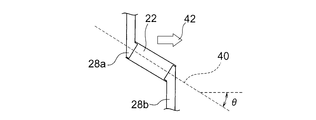
図14は一つの検出電極22とそれに接続された出力配線28a、28bを拡大して上方から見た図である。二つの出力配線28a、28b間に生じる起電力Voutの大きさは、検出電極22と出力配線28a、28bのそれぞれとを接続する2か所の中心を結んだ直線40と磁性層18の磁化方向42との、磁性層18の面内においてなす角度をθとし、検出電極22の直下での磁性層18を伝搬するスピン波の振幅強度をAとすると、角度θと、振幅強度Aに依存する。すなわち、起電力Voutは、Asinθに比例する。この関係を利用すれば、同じ強度のスピン波に対するそれぞれの検出電極22のスピン波信号から電気信号への変換係数を角度θによって変えることができ、重み付けを実現することができる。以下ではi番目の検出電極に対する変換係数をwiと表現する。
第2実施形態のスピン波デバイス1Aを有限インパルス応答フィルタに適用した例を図15に示す。図6に示した場合と同様に、スピン波の伝搬方向を基準とした検出電極間の距離(検出電極の中心間距離)は入力信号の時間間隔t0とスピン波の群速度Vgの積の値になるように配置されることが望ましい。磁場、電場、光などの外場を磁性層18に与えてその磁気特性を変調すると群速度も変化する。変調後の群速度をVg’とすると、本実施形態は、時間間隔t0’=d/Vg’の信号に対して元の周波数特性とは異なる特性を持ったフィルタとして動作させることもできる。
なお、スピン波を生成する部分は第1実施形態と同様であり、図13に示すように磁性層18と下地層12との間に磁性層18に隣接したトンネルバリア層16もしくは非磁性導電層17、さらにトンネルバリア層16もしくは非磁性導電層17隣接した磁性層15、この磁性層15に隣接した反強磁性層14を持つ構造、もしくは図8、9に示すように入力電極が多層膜構造になっているような形態をとってもよい。第1実施形態と同様の方法で生成されたスピン波インパルス信号は距離に応じた遅延時間後、各検出電極の位置まで到達して変換係数wiに応じた電気信号へ変換される。各検出電極に接続されている2本の出力配線28a、28bは各々出力端子A、Bに接続されており、すべての検出電極22から生じる信号を電気的合算して外部へ出力される。負の重み付けはそれぞれの出力端子に接続されている出力配線の接続位置を入れ替えることで実現される。精度よく大きな信号を得るために、各検出電極の抵抗は出力端子に接続される後段の回路の入力インピーダンスより十分に大きいことが望ましい。
本実施形態に接続される周辺回路の構成上の理由から、グラウンドループによるノイズ発生を抑えたい場合は、図16に示すように、検出電極22と磁性層18との間にトンネルバリア層23を挿入することもできる。その場合、トンネルバリア層23の厚さを約0.2nm~2.0nm程度の範囲内の値とすると、スピンポンピングの効果を維持しつつグラウンドループの影響を最小限に抑えることができる。
図14、15においては長方形の検出電極を一例としたが、スピンホール効果による起電力に対する重み付けを容易に設計する観点に立てば、その面内形状は2回の回転対称性もしくは円に代表される高次の回転対称性を有していることが望ましい。
以上説明したように、本実施形態によれば、磁性層18にインパルス入力電気信号によるスピン波インパルス信号を発生させ、伝搬してきた異なるタイミングで検出電極に入力される信号を電気信号に変換し合算することで、有限インパルス応答を示す高速動作素子を実現することができる。したがって、LSIに集積化が可能でかつ周波数特性の設計自由度の高いスピン波デバイスを実現することができる。
(第1実施例)
次に、本発明の第1実施例について図4および図6を参照して説明する。この実施例は図4および図6に示すように絶縁層24を貫通して磁性層18に隣接する10個の入力電極201~2010と、同様に絶縁層24を貫通して磁性層18に達する9個の検出電極221~229を備えている、タップ数N=9の有限インパルス応答低周波数域透過型フィルタである。入力電極201~2010のそれぞれの直径は50nmである。設計に当たっては目標の特性として、サンプリング周波数fs=3.3GHzのインパルス列からなる包絡線信号に対して、遮断周波数fc=1GHzを想定した。ここでは入力電極側から近い順に数えて検出電極221~検出電極229と呼ぶ。中間の検出電極225は基準となる検出電極であって、その直径は100nmである。他の検出電極An(n=1,2,3,4,6,7,8,9)の面積Anは検出電極225の面積A5を基準として次式で設定している。

ここで、遮断角振動数ωc=2πfc、サンプリング周期T=1/fsである。上記の値が正になる場合は、図6において紙面に向かって下方の検出電極に接続され、負の場合は上方の出力配線に接続される。検出電極の間隔は、スピン波の群速度として1μm/nsec、サンプリング周期Tとして300psを想定して300nmとした。
次に、本発明の第1実施例について図4および図6を参照して説明する。この実施例は図4および図6に示すように絶縁層24を貫通して磁性層18に隣接する10個の入力電極201~2010と、同様に絶縁層24を貫通して磁性層18に達する9個の検出電極221~229を備えている、タップ数N=9の有限インパルス応答低周波数域透過型フィルタである。入力電極201~2010のそれぞれの直径は50nmである。設計に当たっては目標の特性として、サンプリング周波数fs=3.3GHzのインパルス列からなる包絡線信号に対して、遮断周波数fc=1GHzを想定した。ここでは入力電極側から近い順に数えて検出電極221~検出電極229と呼ぶ。中間の検出電極225は基準となる検出電極であって、その直径は100nmである。他の検出電極An(n=1,2,3,4,6,7,8,9)の面積Anは検出電極225の面積A5を基準として次式で設定している。
この実施例の有限インパルス応答低周波数域透過型フィルタは図4に示す積層構造を有している。磁性層18としてCoFeB、トンネルバリア層16としてMgO、磁性層15としてCoFe/CoFeBの2層積層構造を用いた。磁性層15はIrMnからなる反強磁性層14により紙面の左から右へ向かうように磁化が固着される。一方、磁性層18の磁化は、外部磁界が存在しない場合に、磁性層15の磁化と反平行となっている。
本実施例の有限インパルス応答フィルタは、以下のように作製される。まず、ウェーハ(基板)10上に下地層12を形成した後、そのウェーハ10を超高真空スパッタ装置内に配置する。次に、下地層12上に、IrMnからなる反強磁性層14、CoFe/CoFeBからなる磁性層15、MgOからなるトンネルバリア層16、CoFeBからなる磁性層18、およびRuからなるキャップ層(図示せず)を、この順序で積層する。そして、磁場中でのアニールによりCoFe/CoFeBからなる磁性層15の磁化を固着させた。また室温中で磁場を印加してCoFeBからなる磁性層18の磁化をCoFe/CoFeBからなる磁性層15の磁化方向と反平行に固着させる。
次に、全面にレジストを塗布し、このレジストを、KrFを用いるステッパ露光装置によってパターニングし、レジスト中にGND電極30に対応する位置に開口を形成する。そして、上記開口が形成されたレジストをマスクとして、イオンミリング法を用いて、GND電極30が形成される領域上の反強磁性層14、磁性層15、トンネルバリア層16、磁性層18、およびRuからなるキャップ層(図示せず)を削り取り、下地層12の上面を露出させる。
次に、上記キャップ層上にEB(electron beam:電子線)レジストを塗布してEB露光を行い、GND電極30、入力電極201~2010、および検出電極221~229に対応した開口をEBレジストに形成する。そして、GND電極30、入力電極201~2010、および検出電極221~229に対応した開口をCuで埋め込み成膜し、EBレジストを除去することにより、GND電極30、入力電極201~2010、および検出電極221~229を形成する。
次に、反強磁性層14/磁性層15/トンネルバリア層16/磁性層18からなる多層膜構造、GND電極30、入力電極201~2010、および検出電極221~229を完全に覆うようにSiO2層24を成膜する。その後、SiO2層24の表面をイオンミリングにより平坦化することでGND電極30、入力電極201~2010、および検出電極221~229の上面を露出させる。
次に、入力電極201~2010および検出電極221~229のそれぞれに接続される入力配線26および出力配線28の形成を行う。入力配線26と出力配線28の形成は、全面にレジストを塗布し、このレジストを、KrFステッパ露光装置を用いてパターニングし、レジスト中に入力電極201~2010および検出電極221~229にそれぞれ接続する開口を形成する。そして、この開口をCuで埋め込み成膜した後、レジストを除去し形成する。なお、予め、入力電極に半値幅200psのパルス状電流を流し、入力電極に接続したスペクトルアナライザーによる信号解析と距離が異なる信号検出電極にて時間分解検出を行って、伝播するスピン波の中心周波数が約12.4GHz、群速度が0.98μm/nsecであることを確認した。
次に、入力電極201~2010と検出電極221~229にそれぞれ定バイアス電圧を印加し、繰り返し周波数が3.3GHz、半値幅が200psインパルスからなるインパルス列を正弦波sin(ωt)で振幅変調した信号を容量カップルを通して入力電極へ入力し、正弦波の周波数を500MHzから1.5GHzまで掃引したところ、1GHzまでは振幅10μAの入力信号と同じ正弦波変調インパルス信号が出力端子から得られたが、1GHzを超えたところで急激に振幅が小さくなり、本実施例の有限インパルス応答低周波数域透過型フィルタが設計通り動作していることを確認できた。
さらに、紙面に向かって下から上方向へ磁性層18の磁化の向きと平行な方向に200Oeの磁場を印加してスピン波の群速度を0.75μm/nsecとした上で、インパルス列の繰り返し周期400psとして同様の実験を行ったところ、750MHzの遮断周波数を得ることができ、印加磁場によってフィルタ特性をチューニングできることも確認した。
(第2実施例)
次に本発明の第2実施例について説明する。本実施例は、図8および図10に示すように、入力電極および検出電極が多層膜構造を有する有限インパルス応答低周波数域透過型フィルタである。入検出電極の大きさと配置、個数は第1実施例と同様である。
次に本発明の第2実施例について説明する。本実施例は、図8および図10に示すように、入力電極および検出電極が多層膜構造を有する有限インパルス応答低周波数域透過型フィルタである。入検出電極の大きさと配置、個数は第1実施例と同様である。
この第2実施例の有限インパルス応答低周波数域透過型フィルタは、次のように作製される。まず、ウェーハ(基板)10上に下地層12を形成した後、そのウェーハ10を超高真空スパッタ装置内に配置する。続いて、下地層12上にCoFeBからなる磁性層18、MgOからなるトンネルバリア層16、CoFeB/CoFeの積層構造を有する磁性層15、IrMnからなる反強磁性層14、およびRuからなるキャップ層(図示せず)を、この順序で堆積させる。そして、磁場中でのアニールによりCoFe/CoFeBからなる磁性層15の磁化を固着させる。その後、磁性層15と、CoFeBからなる磁性層18の磁化の向きが互いに反平行となるように室温中で磁場を印加して磁性層18の磁化を固着した。
次に、全面にレジストを塗布し、KrFを用いたステッパ露光装置によって、上記レジストをパターニングし、上記レジストにGND電極30が形成される領域に開口を形成する。続いて、上記開口が形成されたレジストをマスクとして、イオンミリング法を用いて、GND電極30が形成される領域上の磁性層18、トンネルバリア層16、磁性層15、および上記キャップ層を削り取り、下地層12の上面を露出させる。
次に、前記レジストパターンを剥離した後、再び全面にEBレジストを塗布し、EB露光を用いてGND電極30、入力電極20、検出電極30の部分だけレジストが残るようにパターニングする。そして、パターニングされたレジストをマスクとして、イオンミリング法を用いて、レジストが残っていない部分においてトンネルバリア層16の上面が露出するまで磁性層15、反強磁性層14、およびキャップ層を削り取る。
さらに、パターニングされたレジストをそのままにSiO2からなる絶縁層24を、スパッタ装置を用いて、トンネルバリア層16の上面が露出している部分に堆積し、イオンミリングで削られなかった入力電極と検出電極が絶縁層24に埋め込まれた状態にする。そして、上記レジストをその上に成膜されているSiO2層ともども剥離する。
次に、再び全面にレジストを塗布して、KrFを用いたステッパ露光装置を用いて入力配線26、出力配線28、GND電極30の配線に相当する部分が開口したレジストパターンを形成する。そして開口部にCuを埋め込み成膜して、レジストを剥離することで、入力配線26、出力配線28、GND配線が形成される。
このようにして作製された有限インパルス応答低周波数域透過型フィルタは第1実施例の有限インパルス応答低周波数域透過型フィルタとほぼ同様の周波数特性を示す一方、入力電極に同じ信号電圧を印加しても3μAの電流しか流れなかった。本実施例の有限インパルス応答低周波数域透過型フィルタは、第1実施例に比べて製造工程が増えるが、電流の閉じ込めが効率よく行うことが可能なため、低消費電力な有限インパルス応答低周波数域透過型フィルタとなる。
(第3実施例)
次に、本発明の第3実施例について説明する。本実施例は図13、14、15に示すように、検出電極のスピン波検出方法にスピンポンピングとスピンホール効果を用いた有限インパルス応答低周波数域透過型フィルタである。検出電極22は入力電極側から近い順に数えて検出電極221~検出電極229の全部で9つあり、形状は図13、14に示すように長方形である。配置は第1実施例と同様である。検出信号の重み付けは図13に示すように磁性層18の磁化方向と検出電極22に生じる起電力を検出する点との位置関係で決まり、図13に示した角度θを中間の検出電極225においては0度とし、その他の検出電極22n(n=1,2,3,4,6,7,8,9)の角度θnは、

とする。積層構造、そして磁性層18と磁性層15の磁化の向きも第1実施例と同様である。
次に、本発明の第3実施例について説明する。本実施例は図13、14、15に示すように、検出電極のスピン波検出方法にスピンポンピングとスピンホール効果を用いた有限インパルス応答低周波数域透過型フィルタである。検出電極22は入力電極側から近い順に数えて検出電極221~検出電極229の全部で9つあり、形状は図13、14に示すように長方形である。配置は第1実施例と同様である。検出信号の重み付けは図13に示すように磁性層18の磁化方向と検出電極22に生じる起電力を検出する点との位置関係で決まり、図13に示した角度θを中間の検出電極225においては0度とし、その他の検出電極22n(n=1,2,3,4,6,7,8,9)の角度θnは、
第3実施例の有限インパルス応答低周波数域透過型フィルタは、次のように作製される。まず、ウェーハ(基板)10上に下地層12を形成した後、そのウェーハ10を超高真空スパッタ装置内に配置する。続いて、下地層12上に、IrMnからなる反強磁性層14、CoFe/CoFeBの積層構造を有する磁性層15、MgOからなるトンネルバリア層16、CoFeBからなる磁性層18、およびRuからなるキャップ層(図示せず)を、この順序で積層する。そして、磁場中でのアニールによりCoFe/CoFeBからなる磁性層15の磁化を例えば図13において紙面の左から右方向へ固着させた。また室温中で磁場を印加してCoFeBからなる磁性層18の磁化を磁性層15の磁化方向と反平行に固着させる。
次に、全面にレジストを塗布し、このレジストを、KrFを用いたステッパ露光装置によってパターニングすることにより、レジスト中にGND電極に対応する位置に開口を形成する。続いて、開口が形成されたレジストをマスクとして、イオンミリング法を用いて、GND電極30が形成される領域上の反強磁性層14、磁性層15、トンネルバリア層16、磁性層18、および上記キャップ層を削り取り、下地層12の上面を露出させる。
次に、上記キャップ層上にEBレジストを塗布してEB露光を行い、EBレジストの、GND電極と入力電極が形成される領域に開口を形成する。そして、GND電極と入力電極が形成される領域に対応した開口をCuで埋め込み成膜し、EBレジストを除去することにより、GND電極と入力電極を形成する。
次に、再度EBレジストを塗布してEB露光を行い、検出電極に対応した開口をEBレジストに形成する。そして、検出電極に対応した開口にスピン軌道相互作用の大きいPtで埋め込み成膜し、EBレジストを除去することで検出電極を形成する。
次に、反強磁性層14/磁性層15/トンネルバリア層16/磁性層18の多層膜構造、GND電極、入力電極、および検出電極を完全に覆うようにSiO2層24を成膜する。その後、SiO2層24の表面を、イオンミリング法を用いて平坦化することでGND電極、入力電極および検出電極の上面を露出させる。
次に、入力電極および検出電極のそれぞれに接続される入力配線と出力配線の形成を行う。入力配線と出力配線の形成は、全面にレジストを塗布し、このレジストを、KrFを用いたステッパ露光装置によってパターニングし、レジスト中に入力電極および検出電極にそれぞれ接続する開口を形成する。そして、この開口をCuで埋め込み成膜した後、レジストを除去し形成する。
このようにして作製された有限インパルス応答低周波数域透過型フィルタは第1実施例の有限インパルス応答低周波数域透過型フィルタとほぼ同様の周波数特性を示した。また、出力信号強度が第1実施例の20%程度と小さかったが、検出電極に外部より電源を接続する必要がなく低消費電力な有限インパルス応答低周波数域透過型フィルタが実現することができた。
以上説明したように、本発明の各実施形態および各実施例によれば、LSIに集積化が可能でかつ周波数特性の設計自由度の高いスピン波デバイスを実現することができる。
1 スピン波デバイス
1A スピン波デバイス
10 基板(ウェーハ)
12 下地層
14 反強磁性層
15 磁性層
16 トンネルバリア層
17 非磁性導電層
18 磁性層
20 入力電極の組
201~20m 入力電極
22 検出電極
221~22n 検出電極
24 絶縁層
26 入力配線
28 出力配線
30 GND電極
1A スピン波デバイス
10 基板(ウェーハ)
12 下地層
14 反強磁性層
15 磁性層
16 トンネルバリア層
17 非磁性導電層
18 磁性層
20 入力電極の組
201~20m 入力電極
22 検出電極
221~22n 検出電極
24 絶縁層
26 入力配線
28 出力配線
30 GND電極
Claims (8)
- 入力インパルス信号を伝える1本の入力配線と、
下地層を含む多層膜と、
前記多層膜上に設けられ前記入力インパルス信号を受けることによりスピン波を発生し、前スピン波を伝搬する第1の磁性層と、
前記第1の磁性層上に一直線上に配列されるとともに前記入力配線に接続され、前記入力インパルス信号を前記第1の磁性層に伝える複数の入力電極と、
前記第1の磁性層中を伝搬した前記スピン波を検出する複数の検出電極であって、前記複数の入力電極が配列された前記直線からの距離が異なるようにそれぞれが前記第1の磁性層上に設けられた複数の検出電極と、
を備え、
前記検出電極の個数をn(n≧2)とし、第i(n≧i≧1)番目の検出電極の前記直線からの距離をLiとし、前記スピン波の群速度をVgとし、前記入力インパルス信号のパルス周期をt0とすると、隣接する第i(n-1≧i≧1)番目の検出電極と第i+1番目の検出電極と間の前記直線に直交する方向における距離dは、
d=Vg×t0
と表されることを特徴とするスピン波デバイス。 - 前記多層膜は、前記第1の磁性層に隣接したスペーサ層と、前記スペーサ層に隣接し、磁化の向きが固定された第2の磁性層とを含むことを特徴とする請求項1記載のスピン波デバイス。
- 前記スペーサ層は、トンネルバリア層であることを特徴とする請求項2記載のスピン波デバイス。
- 前記スペーサ層は、非磁性導電層であることを特徴とする請求項2記載のスピン波デバイス。
- 前記入力電極のそれぞれは、前記第1の磁性層に隣接したスペーサ層と、前記スペーサ層に隣接し、磁化の向きが固定された第2の磁性層を含むことを特徴とする請求項1記載のスピン波デバイス。
- 前記検出電極のそれぞれは、前記第1の磁性層に隣接したスペーサ層と、前記スペーサ層に隣接し、磁化の向きが固定された第2の磁性層を含むことを特徴とする請求項1記載のスピン波デバイス。
- 2本の出力配線を有し、前記複数の検出電極のそれぞれは、前記2本の出力配線と異なる接続点で接続されることを特徴とする請求項1記載のスピン波デバイス。
- 前記複数の検出電極のそれぞれは、前記第1の磁性層と間にトンネルバリア層が設けられていることを特徴とする請求項1記載のスピン波デバイス。
Priority Applications (3)
| Application Number | Priority Date | Filing Date | Title |
|---|---|---|---|
| PCT/JP2010/050624 WO2011089692A1 (ja) | 2010-01-20 | 2010-01-20 | スピン波デバイス |
| JP2011550744A JP5389950B2 (ja) | 2010-01-20 | 2010-01-20 | スピン波デバイス |
| US13/487,769 US8917152B2 (en) | 2010-01-20 | 2012-06-04 | Spin wave device |
Applications Claiming Priority (1)
| Application Number | Priority Date | Filing Date | Title |
|---|---|---|---|
| PCT/JP2010/050624 WO2011089692A1 (ja) | 2010-01-20 | 2010-01-20 | スピン波デバイス |
Related Child Applications (1)
| Application Number | Title | Priority Date | Filing Date |
|---|---|---|---|
| US13/487,769 Continuation US8917152B2 (en) | 2010-01-20 | 2012-06-04 | Spin wave device |
Publications (1)
| Publication Number | Publication Date |
|---|---|
| WO2011089692A1 true WO2011089692A1 (ja) | 2011-07-28 |
Family
ID=44306515
Family Applications (1)
| Application Number | Title | Priority Date | Filing Date |
|---|---|---|---|
| PCT/JP2010/050624 Ceased WO2011089692A1 (ja) | 2010-01-20 | 2010-01-20 | スピン波デバイス |
Country Status (3)
| Country | Link |
|---|---|
| US (1) | US8917152B2 (ja) |
| JP (1) | JP5389950B2 (ja) |
| WO (1) | WO2011089692A1 (ja) |
Cited By (3)
| Publication number | Priority date | Publication date | Assignee | Title |
|---|---|---|---|---|
| JP2013120915A (ja) * | 2011-12-09 | 2013-06-17 | Hitachi Ltd | スピン波導波路、及びスピン波演算回路 |
| WO2014038015A1 (ja) * | 2012-09-05 | 2014-03-13 | 株式会社日立製作所 | スピン波スイッチ、及びそれを用いたfpga |
| CN107104181A (zh) * | 2016-02-23 | 2017-08-29 | Tdk株式会社 | 磁阻效应器件 |
Families Citing this family (4)
| Publication number | Priority date | Publication date | Assignee | Title |
|---|---|---|---|---|
| US9797963B2 (en) * | 2014-03-25 | 2017-10-24 | Allegro Microsystems, Llc | Systems and methods for a magnetic target with magnetic bias field |
| CN104779274B (zh) * | 2015-03-10 | 2017-12-01 | 复旦大学 | 一种具有单向导通特性的自旋波二极管 |
| EP3249705B1 (en) | 2016-05-24 | 2019-12-18 | IMEC vzw | Tunable magnonic crystal device and filtering method |
| US11243276B2 (en) * | 2018-09-06 | 2022-02-08 | The Regents Of The University Of California | Magnetometer based on spin wave interferometer |
Citations (2)
| Publication number | Priority date | Publication date | Assignee | Title |
|---|---|---|---|---|
| JP2005176318A (ja) * | 2003-11-19 | 2005-06-30 | Matsushita Electric Ind Co Ltd | 電気機械フィルタ |
| JP2007124340A (ja) * | 2005-10-28 | 2007-05-17 | Toshiba Corp | 高周波発振素子、ならびにそれを用いた車載レーダー装置、車間通信装置および情報端末間通信装置 |
Family Cites Families (8)
| Publication number | Priority date | Publication date | Assignee | Title |
|---|---|---|---|---|
| US4679012A (en) * | 1986-03-31 | 1987-07-07 | Westinghouse Electric Corp. | Magnetostatic-wave device |
| JPH04115701A (ja) * | 1990-09-05 | 1992-04-16 | Hitachi Metals Ltd | 静磁波素子 |
| US5283541A (en) * | 1991-03-29 | 1994-02-01 | Murata Manufacturing Co., Ltd. | Magnetostatic wave device having a multi-portion holder |
| US7528688B2 (en) * | 2005-07-29 | 2009-05-05 | Oakland University | Ferrite-piezoelectric microwave devices |
| KR100819142B1 (ko) | 2005-09-29 | 2008-04-07 | 재단법인서울대학교산학협력재단 | 강한 스핀파 발생 방법 및 스핀파를 이용한 초고속 정보처리 스핀파 소자 |
| US7535070B2 (en) | 2006-01-30 | 2009-05-19 | The Regents Of The University Of California | Spin-wave architectures |
| US20100075599A1 (en) * | 2008-09-22 | 2010-03-25 | Haiwen Xi | Data Transmission and Exchange Using Spin Waves |
| JP5155907B2 (ja) | 2009-03-04 | 2013-03-06 | 株式会社東芝 | 磁性膜を用いた信号処理デバイスおよび信号処理方法 |
-
2010
- 2010-01-20 WO PCT/JP2010/050624 patent/WO2011089692A1/ja not_active Ceased
- 2010-01-20 JP JP2011550744A patent/JP5389950B2/ja not_active Expired - Fee Related
-
2012
- 2012-06-04 US US13/487,769 patent/US8917152B2/en not_active Expired - Fee Related
Patent Citations (2)
| Publication number | Priority date | Publication date | Assignee | Title |
|---|---|---|---|---|
| JP2005176318A (ja) * | 2003-11-19 | 2005-06-30 | Matsushita Electric Ind Co Ltd | 電気機械フィルタ |
| JP2007124340A (ja) * | 2005-10-28 | 2007-05-17 | Toshiba Corp | 高周波発振素子、ならびにそれを用いた車載レーダー装置、車間通信装置および情報端末間通信装置 |
Non-Patent Citations (2)
| Title |
|---|
| SANG-KOOG KIM ET AL.: "A gigahertz-range spin-wave filter composed of width-modulated nanostrip magnonic-crystal waveguides", APPLIED PHYSICS LETTERS, vol. 95, no. 8, 24 August 2009 (2009-08-24), pages 082507 * |
| Y.J.ATAIIYAN ET AL.: "MSSW TRANSVERSAL FILTERS BASED ON CURRENT WEIGHTING IN NARROW (10pm) TRANSDUCERS", IEEE MTT-S DIGEST, 1986, pages 575 - 578 * |
Cited By (4)
| Publication number | Priority date | Publication date | Assignee | Title |
|---|---|---|---|---|
| JP2013120915A (ja) * | 2011-12-09 | 2013-06-17 | Hitachi Ltd | スピン波導波路、及びスピン波演算回路 |
| WO2014038015A1 (ja) * | 2012-09-05 | 2014-03-13 | 株式会社日立製作所 | スピン波スイッチ、及びそれを用いたfpga |
| CN107104181A (zh) * | 2016-02-23 | 2017-08-29 | Tdk株式会社 | 磁阻效应器件 |
| CN107104181B (zh) * | 2016-02-23 | 2020-01-03 | Tdk株式会社 | 磁阻效应器件 |
Also Published As
| Publication number | Publication date |
|---|---|
| US8917152B2 (en) | 2014-12-23 |
| US20120280769A1 (en) | 2012-11-08 |
| JPWO2011089692A1 (ja) | 2013-05-20 |
| JP5389950B2 (ja) | 2014-01-15 |
Similar Documents
| Publication | Publication Date | Title |
|---|---|---|
| JP5155907B2 (ja) | 磁性膜を用いた信号処理デバイスおよび信号処理方法 | |
| JP5389950B2 (ja) | スピン波デバイス | |
| CN107104181B (zh) | 磁阻效应器件 | |
| JP5278876B2 (ja) | マイクロ波発振素子および検出素子 | |
| JP6429871B2 (ja) | 磁気抵抗ミキサ | |
| US9019757B2 (en) | Spin wave element | |
| JP4633689B2 (ja) | マイクロ波発振素子及びその製造方法、並びに該マイクロ波発振素子を備えたマイクロ波発振装置 | |
| JPWO2018052062A1 (ja) | 磁気抵抗効果デバイスおよび磁気抵抗効果モジュール | |
| CN107689363A (zh) | 磁电阻效应器件 | |
| US20180068703A1 (en) | Magnonic holographic memory and methods | |
| JP5790360B2 (ja) | 周波数選択性を有する混合器 | |
| He et al. | Integrated magnetics and magnetoelectrics for sensing, power, RF, and microwave electronics | |
| WO2010097997A1 (ja) | 磁性発振素子 | |
| US20190228894A1 (en) | Magnetoresistance effect device | |
| Fu et al. | Enhancing radiation in magnetoacoustic coupling SAW devices via FeGaB thin-film and focused interdigital transducers on a LiNbO 3/SiO 2/Si substrate | |
| JP5790359B2 (ja) | 混合器 | |
| JP5701628B2 (ja) | スピン波素子 | |
| JP2012060033A (ja) | スピン波素子 | |
| JP3990386B2 (ja) | マイクロ波伝送線路およびマイクロ波フィルタ | |
| CN106559039B (zh) | 磁阻效应器件 | |
| KR101825174B1 (ko) | 스커미온을 이용한 신호 전달 소자 | |
| JP7087587B2 (ja) | 磁気抵抗効果デバイス | |
| JP2018046080A (ja) | 共振素子、共振器および磁気抵抗効果デバイス | |
| JP2015201515A (ja) | 薄膜磁性素子およびそれを備えた高周波デバイス | |
| JP2020047965A (ja) | 共振器 |
Legal Events
| Date | Code | Title | Description |
|---|---|---|---|
| 121 | Ep: the epo has been informed by wipo that ep was designated in this application |
Ref document number: 10843858 Country of ref document: EP Kind code of ref document: A1 |
|
| WWE | Wipo information: entry into national phase |
Ref document number: 2011550744 Country of ref document: JP |
|
| NENP | Non-entry into the national phase |
Ref country code: DE |
|
| 122 | Ep: pct application non-entry in european phase |
Ref document number: 10843858 Country of ref document: EP Kind code of ref document: A1 |