WO2011077965A1 - 露光装置 - Google Patents
露光装置 Download PDFInfo
- Publication number
- WO2011077965A1 WO2011077965A1 PCT/JP2010/072172 JP2010072172W WO2011077965A1 WO 2011077965 A1 WO2011077965 A1 WO 2011077965A1 JP 2010072172 W JP2010072172 W JP 2010072172W WO 2011077965 A1 WO2011077965 A1 WO 2011077965A1
- Authority
- WO
- WIPO (PCT)
- Prior art keywords
- switching element
- light
- beam spot
- beam spots
- exposure apparatus
- Prior art date
- Legal status (The legal status is an assumption and is not a legal conclusion. Google has not performed a legal analysis and makes no representation as to the accuracy of the status listed.)
- Ceased
Links
Images








Classifications
-
- H—ELECTRICITY
- H10—SEMICONDUCTOR DEVICES; ELECTRIC SOLID-STATE DEVICES NOT OTHERWISE PROVIDED FOR
- H10P—GENERIC PROCESSES OR APPARATUS FOR THE MANUFACTURE OR TREATMENT OF DEVICES COVERED BY CLASS H10
- H10P76/00—Manufacture or treatment of masks on semiconductor bodies, e.g. by lithography or photolithography
- H10P76/20—Manufacture or treatment of masks on semiconductor bodies, e.g. by lithography or photolithography of masks comprising organic materials
- H10P76/204—Manufacture or treatment of masks on semiconductor bodies, e.g. by lithography or photolithography of masks comprising organic materials of organic photoresist masks
- H10P76/2041—Photolithographic processes
-
- G—PHYSICS
- G03—PHOTOGRAPHY; CINEMATOGRAPHY; ANALOGOUS TECHNIQUES USING WAVES OTHER THAN OPTICAL WAVES; ELECTROGRAPHY; HOLOGRAPHY
- G03F—PHOTOMECHANICAL PRODUCTION OF TEXTURED OR PATTERNED SURFACES, e.g. FOR PRINTING, FOR PROCESSING OF SEMICONDUCTOR DEVICES; MATERIALS THEREFOR; ORIGINALS THEREFOR; APPARATUS SPECIALLY ADAPTED THEREFOR
- G03F7/00—Photomechanical, e.g. photolithographic, production of textured or patterned surfaces, e.g. printing surfaces; Materials therefor, e.g. comprising photoresists; Apparatus specially adapted therefor
- G03F7/70—Microphotolithographic exposure; Apparatus therefor
- G03F7/70383—Direct write, i.e. pattern is written directly without the use of a mask by one or multiple beams
- G03F7/704—Scanned exposure beam, e.g. raster-, rotary- and vector scanning
Definitions
- the present invention relates to an exposure apparatus that generates a predetermined light / dark pattern by driving a switching element made of an electro-optic crystal material, and exposes the light / dark pattern on an object to be exposed. Specifically, the exposure position is controlled in an analog manner.
- the present invention relates to an exposure apparatus that attempts to improve exposure pattern positioning accuracy.
- a predetermined pattern is generated by a pattern generator having a plurality of switching elements made of electro-optic crystal material arranged in a two-dimensional plane, and the pattern is applied to an object being conveyed in one direction.
- the pattern generator includes a plurality of switching elements arranged in a straight line at a predetermined pitch in a direction orthogonal to the conveyance direction of the object to be exposed, in the conveyance direction of the object to be exposed.
- a plurality of rows are arranged at predetermined intervals, and adjacent switching element rows are arranged by being shifted by a predetermined amount in a direction orthogonal to the conveyance direction of the object to be exposed (see, for example, Patent Document 1).
- an object of the present invention is to provide an exposure apparatus that addresses such problems and attempts to improve the exposure pattern positioning accuracy by controlling the exposure position in an analog manner.
- an exposure apparatus comprises a beam spot generating means for generating a plurality of beam spots by receiving light from a light source and arranging them in at least two rows alternately at a predetermined interval, and the plurality of beam spots.
- Optical scanning means for reciprocating scanning within a predetermined range in the alignment direction of the plurality of beam spots, a center axis corresponding to the center of reciprocal scanning of the plurality of beam spots, respectively, and a pair of electrodes on opposing surfaces parallel to the central axis
- a pattern generator for generating a predetermined light / dark pattern by optically modulating the light source light by driving on / off a plurality of switching elements made of a prismatic electro-optic crystal material provided with a light source;
- a projection lens that projects onto the body, and sets the width of the beam spot in the scanning direction of each switching element to the beam spot. It is made larger than the width.
- a plurality of beam spots are generated by receiving light source light from the beam spot generating means and arranged in at least two rows alternately at a predetermined interval, and the plurality of beam spots are respectively arranged in the arrangement direction by the optical scanning means.
- the light source light is optically modulated to generate a predetermined light / dark pattern, and the light / dark pattern is projected onto the object to be exposed by the projection lens.
- the width of the beam spot in the scanning direction of each switching element is made larger than the width of the beam spot in the same direction, the beam spot is scanned on the switching element, and the drive timing of the switching element is controlled to thereby expose the object to be exposed.
- the position of the upper light / dark pattern is controlled in an analog manner.
- the beam spot generating means is a microlens array having a plurality of condensing lenses arranged in a plane. Accordingly, a plurality of beam spots are generated by a microlens array having a plurality of condensing lenses arranged in a plane.
- the beam spot generating means is a photomask having a plurality of openings arranged in a plane. As a result, a plurality of beam spots are generated by a photomask having a plurality of openings arranged in a plane.
- the optical scanning means includes a pair of strip-shaped electrodes having a predetermined width on opposite side surfaces of the rectangular block-shaped electro-optic crystal material, and a longitudinal central axis thereof and a central axis of one of the vertical and horizontal sides of the side surface having a predetermined angle. Are formed so that light passes between the pair of electrodes.
- a pair of band-shaped electrodes having a predetermined width are inclined on the opposite side surfaces of the square block-shaped electro-optic crystal material so that the longitudinal central axis thereof and the vertical or horizontal central axis of the side surface form a predetermined angle.
- a plurality of beam spots are reciprocally scanned within a predetermined range by an optical scanning means formed and configured to allow light to pass between the pair of electrodes.
- the object to be exposed is continuously moved in a direction substantially orthogonal to the scanning direction of the beam spot.
- exposure is performed while continuously moving the object to be exposed in a direction substantially orthogonal to the beam spot scanning direction.
- the beam spot in the scanning direction of the switching element is larger than the width of the beam spot in the same direction, the beam spot can be scanned on the switching element. it can. Therefore, by controlling the driving timing of the switching elements, the position of the light / dark pattern formed on the object to be exposed by light modulation by the plurality of switching elements can be controlled in an analog manner. Thereby, even with a simple pattern generator having a plurality of switching elements arranged in at least two rows, the exposure pattern positioning accuracy can be improved and the manufacturing cost of the apparatus can be reduced.
- the light source light can be condensed to generate a beam spot, and the utilization efficiency of the light source light can be improved. Therefore, the power of the light source to be used can be reduced, and the burden on the light source can be reduced.
- a plurality of beam spots can be generated by a photomask formed using photolithography technology. Therefore, the shape and position of the plurality of beam spots can be formed with high accuracy, and the positioning accuracy of the exposure pattern can be further improved.
- the scanning of the beam spot can be controlled by the drive voltage. Therefore, if the correlation between the position of the beam spot on the switching element and the driving voltage is taken in advance, the position of the beam spot on the switching element can be known by the driving voltage, and the driving timing of the switching element is controlled by the driving voltage. can do.
- FIG. 1 It is a schematic diagram which shows embodiment of the exposure apparatus by this invention. It is a top view which shows the example of 1 structure of the color filter board
- FIG. 1 is a schematic view showing an embodiment of an exposure apparatus according to the present invention.
- the exposure apparatus drives a switching element made of an electro-optic crystal material to generate a predetermined light / dark pattern, and exposes the light / dark pattern on an object to be exposed.
- the conveying means 1, the exposure optical unit 2, An imaging unit 3 and a control unit 4 are provided.
- the object to be exposed is a color filter substrate.
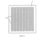
- FIG. 2 is a plan view of the color filter substrate 5 used in the exposure apparatus of the present invention.
- This color filter substrate 5 is formed by forming a black matrix provided with a plurality of pixels 6 transmitting light in a matrix on the surface of a transparent glass substrate.
- the transport means 1 is configured to place the color filter substrate 5 coated with a predetermined color resist on the upper surface of the stage 7 and continuously transport it in one direction (in the direction of arrow A shown in FIG. 1).
- the stage 7 is moved by a moving mechanism configured by combining a gear and the like.
- the surface of the stage 7 is provided with a gas outlet and suction port, and the color filter substrate 5 is transported in a state where it floats on the stage 7 by a predetermined amount by balancing the gas output and suction force. May be.
- the transport unit 1 is provided with a position sensor (not shown) for measuring the moving distance of the color filter substrate 5.
- An exposure optical unit 2 is provided above the conveying means 1.
- the exposure optical unit 2 modulates the light source light L 1 to generate exposure light L 2 having a predetermined light / dark pattern, and irradiates the surface of the color filter substrate 5 with the exposure light L 2 .
- the color resist on the corresponding pixel 6 is exposed, and the light source device 8, the beam spot generating means 9, the optical scanning means 10, the pattern generator 11, and the projection lens 12 are arranged from the upstream side in the light traveling direction. Prepare in order.
- the light source device 8 irradiates the beam spot generating means 9 described later with the parallel light of the light source light L 1 having a uniform luminance distribution.
- the light source device 8 emits ultraviolet light and the laser light source emits the light.
- a beam expander for enlarging the source light L 1 of the light flux diameter which is, with, for example photo integrator beam diameter causes uniform the luminance distribution of the source light L 1 that has been enlarged, the source light L 1 that the luminance distribution is uniformized
- a condenser lens that converts the light into parallel light.
- the beam spot generating means 9 receives the light source light L 1 and generates a plurality of beam spots by arranging them in at least two rows in an array pitch W 1 in a direction orthogonal to the substrate transport direction indicated by arrow A in FIG. Specifically, as shown in FIG. 3, a microlens array having a plurality of condensing lenses 13 arranged in, for example, two rows on the surface of a transparent substrate 14. In this case, the interval between the two lens rows 15 is set to W2. In addition, a light shielding film 16 is formed around each condenser lens 13 to block light transmission.
- the optical scanning means 10 respectively has a plurality of beam spots generated by the beam spot generation means 9 in a direction (arrangement direction of the plurality of condenser lenses 13) orthogonal to the substrate transport direction (arrow A direction).
- a pair of strip-shaped electrodes 18 having a predetermined width are formed on the opposing side surface 17a of the square block-shaped electro-optic crystal material 17 as shown in FIG.
- the side surface 17a is formed so as to be inclined with respect to one of the vertical and horizontal central axes so that light passes between the pair of electrodes 18.
- the pattern generator 11 is controlled by the control means 4 (see FIG. 10), which will be described later, and modulates the light source light L 1 to generate a predetermined light / dark pattern (exposure light L 2 ).
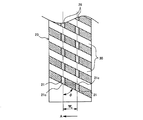
- the center axis is aligned with the center of the reciprocating scanning of the plurality of beam spots 19, and the scanning direction of the beam spot 19 indicated by arrows B and C in FIG. 5 (indicated by the arrow A in FIG. 1).
- a width W 3 (in this embodiment) corresponding to the scanning direction (arrow B, C direction) of the beam spot 19 is arranged in two rows alternately in the arrangement pitch W 1 in the direction orthogonal to the substrate transport direction.
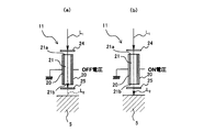
- the pattern generator 11 includes a switching element assembly 23 including the plurality of switching elements 21, a polarizing plate 24 disposed in the vicinity of the incident side end face of the optical scanning unit 10, and an emission of the switching element assembly 23. And a polarizing plate 25 arranged close to the side end face.
- the two polarizing plates 24 and 25 have a crossed Nicols arrangement in which the polarization axes are orthogonal to each other.
- the pattern generator 11 configured as described above operates as follows. That is, as shown in FIG. 6, the light source light L 1 that has passed through the condenser lens 13 of the beam spot generating unit 9 is linearly polarized by the polarizing plate 24 and then enters the incident side end face 21 a of the switching element 21. . In this case, as shown in FIG. 5A, when no voltage is applied to the electrode 20 of the switching element 21, the switching element 21 is driven to turn off, and the polarization plane of the linearly polarized light passing through the switching element 21 is rotated. Not.
- the polarization plane of the linearly polarized light emitted from the emission side end face 21 b of the switching element 21 is orthogonal to the polarization axis of the polarizing plate 25, and the linearly polarized light is blocked by the polarizing plate 25.
- the polarization plane of linearly polarized light passing through the switching element 21 is 90 °. It is rotated. Therefore, the polarization plane of the linearly polarized light emitted from the emission side end face 21 b of the switching element 21 coincides with the polarization axis of the polarizing plate 25, and the linearly polarized light passes through the polarizing plate 25.
- the pattern generator 11 by driving on and off according to the plurality of switching elements 21 in a predetermined pattern, can be injected to generate the exposure light L 2 which is optically modulated light and dark.
- a method for forming the switching element assembly 23 will be described with reference to FIG. First, on one surface of a strip-shaped plate material 26 made of an electro-optic crystal material as shown in FIG. 7A, a dicing saw is used, as shown in FIG. the grooves 27 are formed of, forming a pair of projecting portions 28 having a width W 5 symmetrically to the longitudinal central axis. At this time, the center line spacing biconvex portion 28 is a distance W 2.
- a conductive film 29 is formed on both side surfaces parallel to the long axis of the pair of convex portions 28 and the bottom surface portion of the groove 27 by a known technique.
- W 5 the separation grooves 30 deeper than the depth D of the grooves 27 are formed at a pitch 2W 3 , and the pair of convex portions 28 are divided into a plurality of pieces to form a plurality of switching elements 21.
- the pair of electrodes 20 of each switching element 21 is the electrode 20 on the longitudinal central axis side of the switching element assembly 23. Becomes the ground electrode.
- FIG. 8 is an explanatory view showing another method for forming the switching element assembly 23.
- a strip-shaped plate material 26 of electro-optic crystal material in which a conductive film 29 is formed on the side surface parallel to the long axis of the pair of convex portions 28 and the bottom surface portion of the groove 27 shown in FIG.
- a dicing saw is used to form a separating groove 30 having a depth deeper than the depth D of the groove 27 with respect to the pair of convex portions 28, and the pair of convex portions 28 are divided into a plurality of portions.
- the projection lens 12 projects the light / dark pattern generated by the pattern generator 11 on the color filter substrate 5 in a reduced scale, and includes an imaging lens 31 and an objective lens 32. .
- An imaging unit 3 is provided on the front side of the exposure optical unit 2 in the substrate transport direction (arrow A direction).
- This imaging means 3 is for imaging the surface of the color filter substrate 5 and is a line camera having a large number of light receiving elements arranged in a straight line substantially orthogonal to the substrate transport direction.
- FIG. 23 is arranged at a distance L from the central axis of the switching element row 22a on the near side in the substrate transport direction.
- the switching element assembly 23 and the imaging unit 3 are positioned and arranged with respect to each other, and the switching element 21A of the switching element assembly 23 corresponds to the positions x 1 to x 2 on the longitudinal center axis of the imaging unit 3.
- the switching element 21B corresponds to the positions x 2 to x 3
- the switching element 21C corresponds to the positions x 3 to x 4
- the switching element 21D corresponds to the positions x 4 to x 5
- the switching element 21E corresponds to the position x. corresponding to 5 ⁇ x 6
- switching element 21F is made to correspond to the position x 6 ⁇ x 7.
- An illumination unit (not shown) is provided on the lower side of the stage 7 so as to face the imaging position of the imaging unit 3, and the imaging position of the color filter substrate 5 is illuminated to illuminate the surface of the substrate by the imaging unit 3. Imaging is possible.
- Control means 4 is provided in electrical connection with the transport means 1, the optical scanning means 10, the switching element assembly 23 of the pattern generator 11, and the imaging means 3. This control means 4 drives each component appropriately, and as shown in FIG. 10, the image processing part 33, the calculating part 34, the memory 35, the conveyance means drive controller 36, and the optical scanning means.
- a drive controller 37, a switching element drive controller 38, and a control unit 39 are provided.
- the image processing unit 33 processes the one-dimensional image of the pixel 6 of the color filter substrate 5 acquired by the imaging unit 3 to detect a position where the luminance changes suddenly, and the position of the edge of the pixel 6 is detected. This is detected as the position.
- the computing unit 34 calculates the moving distance of the color filter substrate 5 based on the output of the position sensor of the transport means 1, and the color filter substrate 5 is preset and stored in a memory 35 described later.
- a drive command is issued to a switching element drive controller 38 described later. Yes.
- the memory 35 stores in advance data of initial setting values such as the power of the laser light source and the distances L, (L + W 2 ) between the imaging means 3 and the switching element arrays 22a, 22b of the switching element assembly 23.
- the calculation result in the calculation unit 34 and the position data of the edge of the pixel 6 detected by the image processing unit 33 are temporarily stored.
- the transport means drive controller 36 drives the moving mechanism of the transport means 1 to continuously move the stage 7 at a constant speed in the direction of arrow A in FIG.
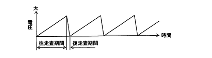
- the optical scanning means drive controller 37 transmits a sawtooth drive signal shown in FIG. 11 to the optical scanning means 10, so that the portion sandwiched between the band-like electrodes 18 of the optical scanning means 10 and the other portions.
- the refractive index difference generated at the interface 17b is continuously changed within a predetermined range, and the beam spot 19 of the laser beam emitted from the optical scanning means 10 is reciprocated within the predetermined range.
- the repetition period of the drive signal is controlled to set the scanning speed of the beam spot 19 to the moving speed of the stage 7 of the transport means 1. (Same as the moving speed of the color filter substrate 5).
- the scanning speed of the beam spot 19 is normally one round trip while the color filter substrate 5 travels a distance W 5 (W 5 is equal to the width of the switching element 21 in the substrate transport direction) or a distance shorter than that. Is set as follows. In the present embodiment, the scanning speed of the beam spot 19 is set sufficiently higher than the moving speed of the color filter substrate 5. Further, the falling speed of the drive signal is controlled to be 10 times the rising speed so that the scanning speed of the beam spot 19 in the backward path is approximately 10 times the scanning speed in the forward path.
- the switching element drive controller 38 receives the drive command transmitted from the calculation unit 34 and sequentially reads the position data of the edge of the pixel 6 stored in the memory 35, and each switching element corresponding to the position data.
- a drive signal for driving the on / off of the motor 21 is transmitted to the switching element assembly 23.
- the switching element driving controller 38 transmits an on / off driving signal to the switching element assembly 23 during the forward scanning period of the beam spot 19 that performs reciprocating scanning, and transmits an off driving signal during the backward scanning period of the beam spot 19. It is like that.
- the control unit 39 is a CPU that mediates the respective elements so as to be driven appropriately.
- the color filter substrate 5 coated with a predetermined color resist is positioned and placed at a predetermined position on the stage 7 of the transport means 1. Thereafter, when the activation switch is turned on, the conveyance means 1 is activated under the control of the conveyance means drive controller 36 of the control means 4, and the color filter substrate 5 is conveyed at a constant speed in the direction of arrow A shown in FIG.
- the surface of the color filter substrate 5 is imaged by the imaging means 3, and this one-dimensional captured image is subjected to image processing in the image processing unit 33 of the control means 4. Is done.
- the image processing unit 33 the luminance change in the direction orthogonal to the substrate transport direction (arrow A direction) of the captured image is checked, and the pixel 6 (bright portion) indicates the position where the luminance has suddenly changed beyond a predetermined threshold. Detect as the edge.
- the captured image captured at this time is captured.
- the positions x 8 , x 9 , x 10 , x 11 ... Of the edge of the pixel 6 (bright part) on the line P 1 are detected, and this position data is stored in the memory 35.
- other colors for example, green, blue, etc.
- Pixels 6G and 6B can be ignored.
- the color filter substrate 5 is conveyed in the direction of arrow A in FIG. 12 (a), the the line P 1 matches the center axis of the switching element array 22a of the switching device assembly 23, the respective switching elements 21 of the switching element array 22a predetermined position on the line P 1 is selectively exposed. That is, between the position x 8, x 3 on line P 1, the position x 4, between x 9 and position x 12, x 13 between the respective switching element 21C, 21E, 21K is exposed in charge. In this case, the switching element 21C is controlled to be turned on by the switching element drive controller 38 only while the beam spot 19 scans between the positions x 8 and x 3 .
- the switching element 21E is turned on for driving while the beam spot 19 is scanning between position x 4, x 9, the switching element 21K, the beam spot 19 scans between position x 12, x 13 It is driven on only while As a result, as shown by cross-hatching in the figure, the region between the positions x 8 and x 3 , the position between the positions x 4 and x 9 and the position between the positions x 12 and x 13 on the pixel 6R is exposed. At this time, the switching elements 21A, 21G, 21I, and 21M of the switching element row 22a are driven off.
- the position of the beam spot 19 on the switching element 21 correlates with the deflection angle ⁇ of the laser beam by the optical scanning means 10, and the deflection angle ⁇ of the laser beam correlates with the drive signal voltage by the optical scanning means drive controller 37. To do. Therefore, the position of the beam spot 19 on the switching element 21 can be known from the drive signal voltage.
- the switching elements 21 of the switching element array 22a are driven in the same manner as described above while reciprocatingly scanning the beam spot 19, and the color filter substrate 5 moving at a constant speed is exposed.
- the imaging sequential position shifted in the arrow A and the opposite direction by the line P 1 distance color filter substrate 5 is equal to the distance moved while the beam spot 19 makes one reciprocation This is performed by driving each of the switching elements 21 based on the image data.
- the switching elements 21 of the switching element array 22a is the position data of the edges of the arrow A and the direction opposite to W 2 shifted by the line P 2 on pixels 6R respect to the line P 1 is read from the memory 35 switching It is driven by the element drive controller 38. Then, the position between the positions x 3 and x 4 of the pixel 6R on the line P 2 is exposed by the switching element 21C, and the position between the positions x 12 and x 13 of the pixel 6R is exposed by the switching element 21K. At this time, the switching elements 21A, 21E, 21G, 21J, and 21M are off-driven.
- a predetermined position on the pixel 6R is exposed in advance by the switching element array 22a while reciprocally scanning the beam spot 19 with respect to the color filter substrate 5 moving at a constant speed, and the switching element array 22b performs the switching element array 22b.
- the portion between the switching elements 21 of 22a is complemented and exposed.
- the pixel 6R is exposed and a predetermined exposure pattern 40 is formed.
- the beam spot scanning speed is sufficiently higher than the moving speed of the color filter substrate 5 as in this embodiment, the edge of the exposure pattern that obliquely intersects the substrate transport direction as shown in FIG. Further, the edge of the circular exposure pattern can be formed smoothly.
- the irradiation position of the beam spot in the direction orthogonal to the substrate transport direction can be controlled in an analog manner, a finer pattern exposure can be performed unlike conventional digital control.
- the switching element assembly 23 is configured by the two switching element arrays 22a and 22b has been described.
- the present invention is not limited to this, and the two switching element arrays 22a. , 22b may be arranged as a set and a plurality of sets may be arranged at a predetermined pitch in the substrate transport direction.
- the area on the pixel 6 of the color filter substrate 5 can be subjected to multiple exposure by the switching elements 21 of the plurality of sets of switching element arrays 22a and 22b, and the power of the laser light source is lowered to reduce the burden on the laser light source. be able to.
- the beam spot generating means 9 is a microlens array.
- the present invention is not limited to this, and the beam spot generating means 9 is a photo having a plurality of openings arranged in a plane. It may be a mask.
- the optical scanning unit 10 has a pair of strip-shaped electrodes 18 having a predetermined width on the opposing side surface 17 a of the square block-shaped electro-optic crystal material 17, and either the longitudinal center axis or the side surface 18 is vertically or horizontally.
- the optical scanning means 10 may be a laser beam such as an electromagnetic actuator or an acousto-optic device. Any device capable of reciprocating scanning may be used.
- the object to be exposed is the color filter substrate 5
- the present invention is not limited to this, and the object to be exposed may be any circuit board, for example.
- Color filter substrate (exposed body) 9 ... beam spot generating means 10 ... scanning means 12 ... projection lens 13 ; condenser lens 17 ... electro-optical crystal material 17a ... opposite sides 18, 20 ... electrode 19 ... beam spot 21, 21A ⁇ 21M ... switching element L 1 ... Light source light L 2 ... exposure light
Landscapes
- Physics & Mathematics (AREA)
- General Physics & Mathematics (AREA)
- Exposure And Positioning Against Photoresist Photosensitive Materials (AREA)
- Exposure Of Semiconductors, Excluding Electron Or Ion Beam Exposure (AREA)
Abstract
Description
先ず、図7(a)に示すような電気光学結晶材料から成る短冊状板材26の一面に、同図(b)に示すように、ダイシングソーを使用してその長軸に平行に深さDの溝27を形成し、長手中心軸に対して対称に幅W5の一対の凸部28を形成する。このとき、両凸部28の中心線間隔は、間隔W2とされている。
続いて、同図(d)に示すように、ブレードの歯厚がW3(=W1)のダイシングソーを使用して上記一対の凸部28の短軸方向に幅W3(W3>W5)で上記溝27の深さDよりも深さの深い分離溝30をピッチ2W3で形成し、一対の凸部28を複数に分断して複数のスイッチング素子21を形成する。このとき、同図(d)において、右側凸部28に対してダイシングソーのブレードを矢印E方向に移動して右側凸部28を分断した後、左側凸部28に対してダイシングソーのブレードを矢印F方向に移動して右側凸部28の隣接する分離溝30間に対応する左側凸部28の部分を残して左側凸部28を分断する。これにより、複数のスイッチング素子21が互い違いに2列に並んだスイッチング素子組立体23が形成される。この場合、長軸方向に延びる中央の溝27の底面部の導電膜29を接地電極端子とすると、各スイッチング素子21の一対の電極20にてスイッチング素子組立体23の長手中心軸側の電極20が接地電極となる。
そして、上記制御部39は、上記各要素が適切に駆動するように仲立ちするもので、CPUである。
先ず、所定のカラーレジストが塗布されたカラーフィルタ基板5を搬送手段1のステージ7上の所定位置に位置決めして載置する。その後、起動スイッチが投入されると制御手段4の搬送手段駆動コントローラ36により制御されて搬送手段1が起動し、カラーフィルタ基板5が図1に示す矢印A方向に一定速度で搬送される。
9…ビームスポット生成手段
10…光走査手段
12…投影レンズ
13…集光レンズ
17…電気光学結晶材料
17a…対向側面
18,20…電極
19…ビームスポット
21,21A~21M…スイッチング素子
L1…光源光
L2…露光光
Claims (5)
- 光源光を受けて所定間隔で互い違いに少なくとも2列に並べて複数のビームスポットを生成するビームスポット生成手段と、
前記複数のビームスポットをそれらの並び方向に夫々所定範囲内で往復走査させる光走査手段と、
前記複数のビームスポットの往復走査の中心に夫々中心軸を合致させて配置され、前記中心軸に平行な対向面に一対の電極を設けた角柱状の電気光学結晶材料から成る複数のスイッチング素子をオン・オフ駆動することにより、前記光源光を光変調して所定の明暗パターンを生成するパターンジェネレータと、
前記明暗パターンを被露光体上に投影する投影レンズと、
を備え、
前記各スイッチング素子の前記ビームスポットの走査方向の幅を前記ビームスポットの同方向の幅よりも大きくしたことを特徴とする露光装置。 - 前記ビームスポット生成手段は、複数の集光レンズを平面内に並べて有するマイクロレンズアレイであることを特徴とする請求項1記載の露光装置。
- 前記ビームスポット生成手段は、複数の開口を平面内に並べて有するフォトマスクであることを特徴とする請求項1記載の露光装置。
- 前記光走査手段は、角型ブロック状の電気光学結晶材料の対向側面に所定幅の一対の帯状電極を、その長手中心軸と前記側面の縦横いずれか一方の中心軸とが所定角度を成すように傾けて形成し、該一対の電極間を光が通過するようにしたものであることを特徴とする請求項1記載の露光装置。
- 前記被露光体は、前記ビームスポットの走査方向と略直交する方向に連続して移動するようにされたことを特徴とする請求項1~4のいずれか1項に記載の露光装置。
Priority Applications (2)
| Application Number | Priority Date | Filing Date | Title |
|---|---|---|---|
| KR1020127012115A KR101813212B1 (ko) | 2009-12-22 | 2010-12-09 | 노광 장치 |
| CN201080058060.9A CN102668025B (zh) | 2009-12-22 | 2010-12-09 | 曝光装置 |
Applications Claiming Priority (2)
| Application Number | Priority Date | Filing Date | Title |
|---|---|---|---|
| JP2009290649A JP5282979B2 (ja) | 2009-12-22 | 2009-12-22 | 露光装置 |
| JP2009-290649 | 2009-12-22 |
Publications (1)
| Publication Number | Publication Date |
|---|---|
| WO2011077965A1 true WO2011077965A1 (ja) | 2011-06-30 |
Family
ID=44195499
Family Applications (1)
| Application Number | Title | Priority Date | Filing Date |
|---|---|---|---|
| PCT/JP2010/072172 Ceased WO2011077965A1 (ja) | 2009-12-22 | 2010-12-09 | 露光装置 |
Country Status (5)
| Country | Link |
|---|---|
| JP (1) | JP5282979B2 (ja) |
| KR (1) | KR101813212B1 (ja) |
| CN (1) | CN102668025B (ja) |
| TW (1) | TWI510865B (ja) |
| WO (1) | WO2011077965A1 (ja) |
Families Citing this family (2)
| Publication number | Priority date | Publication date | Assignee | Title |
|---|---|---|---|---|
| JP2016122676A (ja) * | 2014-12-24 | 2016-07-07 | 株式会社アドバンテスト | 露光装置および露光方法 |
| CN117192913B (zh) * | 2023-09-11 | 2025-05-16 | 安徽工程大学 | 一种基于三维移动曝光提高光刻分辨率的系统及方法 |
Citations (4)
| Publication number | Priority date | Publication date | Assignee | Title |
|---|---|---|---|---|
| JP2006163419A (ja) * | 2004-12-07 | 2006-06-22 | Asml Holding Nv | 電気光学変調器を使用するシステムおよび方法 |
| JP2007310251A (ja) * | 2006-05-22 | 2007-11-29 | V Technology Co Ltd | 露光装置 |
| JP2008209568A (ja) * | 2007-02-26 | 2008-09-11 | Seiko Epson Corp | 電気光学素子及び走査型光学装置 |
| JP2009229675A (ja) * | 2008-03-21 | 2009-10-08 | V Technology Co Ltd | 光変調素子 |
Family Cites Families (2)
| Publication number | Priority date | Publication date | Assignee | Title |
|---|---|---|---|---|
| EP1944654A3 (en) * | 1996-11-28 | 2010-06-02 | Nikon Corporation | An exposure apparatus and an exposure method |
| JP2007031025A (ja) | 2005-07-25 | 2007-02-08 | Kyocera Mita Corp | カール矯正装置及びそれを用いた画像形成装置 |
-
2009
- 2009-12-22 JP JP2009290649A patent/JP5282979B2/ja not_active Expired - Fee Related
-
2010
- 2010-12-09 KR KR1020127012115A patent/KR101813212B1/ko not_active Expired - Fee Related
- 2010-12-09 CN CN201080058060.9A patent/CN102668025B/zh not_active Expired - Fee Related
- 2010-12-09 WO PCT/JP2010/072172 patent/WO2011077965A1/ja not_active Ceased
- 2010-12-21 TW TW099144867A patent/TWI510865B/zh not_active IP Right Cessation
Patent Citations (4)
| Publication number | Priority date | Publication date | Assignee | Title |
|---|---|---|---|---|
| JP2006163419A (ja) * | 2004-12-07 | 2006-06-22 | Asml Holding Nv | 電気光学変調器を使用するシステムおよび方法 |
| JP2007310251A (ja) * | 2006-05-22 | 2007-11-29 | V Technology Co Ltd | 露光装置 |
| JP2008209568A (ja) * | 2007-02-26 | 2008-09-11 | Seiko Epson Corp | 電気光学素子及び走査型光学装置 |
| JP2009229675A (ja) * | 2008-03-21 | 2009-10-08 | V Technology Co Ltd | 光変調素子 |
Also Published As
| Publication number | Publication date |
|---|---|
| JP2011134767A (ja) | 2011-07-07 |
| CN102668025A (zh) | 2012-09-12 |
| KR20120112396A (ko) | 2012-10-11 |
| TW201131318A (en) | 2011-09-16 |
| JP5282979B2 (ja) | 2013-09-04 |
| CN102668025B (zh) | 2015-01-28 |
| KR101813212B1 (ko) | 2017-12-29 |
| TWI510865B (zh) | 2015-12-01 |
Similar Documents
| Publication | Publication Date | Title |
|---|---|---|
| US9122171B2 (en) | Exposure apparatus | |
| KR101792302B1 (ko) | 배향 처리 방법 및 배향 처리 장치 | |
| CN103858208A (zh) | 曝光装置用的对准装置以及对准标记 | |
| CN102687077A (zh) | 光学成像写入系统 | |
| CN103415810A (zh) | 曝光装置 | |
| JP5354803B2 (ja) | 露光装置 | |
| CN216351771U (zh) | 一种直写式光刻机的光学系统 | |
| JP5282979B2 (ja) | 露光装置 | |
| JP2006208432A (ja) | 露光方法および装置 | |
| KR101688127B1 (ko) | 노광 장치 | |
| JP2012145613A (ja) | 露光装置 | |
| CN211979422U (zh) | 一种基于扫描拼接的大尺寸曝光光源 | |
| WO2012063607A1 (ja) | 露光装置 | |
| JP2004062157A (ja) | 光配線回路の製造方法、及びその光配線回路を備えた光配線基板 | |
| KR20030091056A (ko) | 레이저장치, 노광헤드, 노광장치 및 광섬유의 접속방법 | |
| WO2020116052A1 (ja) | 投影装置及び三次元計測装置 | |
| US9921482B2 (en) | Exposure device and lighting unit | |
| US20130242281A1 (en) | Exposure apparatus | |
| JP6847088B2 (ja) | 投影装置及び三次元計測装置 | |
| JP5344730B2 (ja) | 露光装置 | |
| WO2005106591A1 (ja) | 露光パターン形成方法 | |
| JP2012211873A (ja) | 3次元計測装置 | |
| TWI386762B (zh) | 曝光裝置及圖形形成方法 | |
| CN116320191A (zh) | 投影图样的形成方法及扫描器 | |
| CN103392150B (zh) | 曝光装置以及微透镜阵列结构体 |
Legal Events
| Date | Code | Title | Description |
|---|---|---|---|
| WWE | Wipo information: entry into national phase |
Ref document number: 201080058060.9 Country of ref document: CN |
|
| 121 | Ep: the epo has been informed by wipo that ep was designated in this application |
Ref document number: 10839199 Country of ref document: EP Kind code of ref document: A1 |
|
| ENP | Entry into the national phase |
Ref document number: 20127012115 Country of ref document: KR Kind code of ref document: A |
|
| NENP | Non-entry into the national phase |
Ref country code: DE |
|
| 122 | Ep: pct application non-entry in european phase |
Ref document number: 10839199 Country of ref document: EP Kind code of ref document: A1 |