WO2011065506A1 - プラズマ処理装置 - Google Patents
プラズマ処理装置 Download PDFInfo
- Publication number
- WO2011065506A1 WO2011065506A1 PCT/JP2010/071171 JP2010071171W WO2011065506A1 WO 2011065506 A1 WO2011065506 A1 WO 2011065506A1 JP 2010071171 W JP2010071171 W JP 2010071171W WO 2011065506 A1 WO2011065506 A1 WO 2011065506A1
- Authority
- WO
- WIPO (PCT)
- Prior art keywords
- frequency
- input
- output
- plasma
- antenna
- Prior art date
- Legal status (The legal status is an assumption and is not a legal conclusion. Google has not performed a legal analysis and makes no representation as to the accuracy of the status listed.)
- Ceased
Links
Images




Classifications
-
- H—ELECTRICITY
- H05—ELECTRIC TECHNIQUES NOT OTHERWISE PROVIDED FOR
- H05H—PLASMA TECHNIQUE; PRODUCTION OF ACCELERATED ELECTRICALLY-CHARGED PARTICLES OR OF NEUTRONS; PRODUCTION OR ACCELERATION OF NEUTRAL MOLECULAR OR ATOMIC BEAMS
- H05H1/00—Generating plasma; Handling plasma
- H05H1/24—Generating plasma
- H05H1/46—Generating plasma using applied electromagnetic fields, e.g. high frequency or microwave energy
-
- C—CHEMISTRY; METALLURGY
- C23—COATING METALLIC MATERIAL; COATING MATERIAL WITH METALLIC MATERIAL; CHEMICAL SURFACE TREATMENT; DIFFUSION TREATMENT OF METALLIC MATERIAL; COATING BY VACUUM EVAPORATION, BY SPUTTERING, BY ION IMPLANTATION OR BY CHEMICAL VAPOUR DEPOSITION, IN GENERAL; INHIBITING CORROSION OF METALLIC MATERIAL OR INCRUSTATION IN GENERAL
- C23C—COATING METALLIC MATERIAL; COATING MATERIAL WITH METALLIC MATERIAL; SURFACE TREATMENT OF METALLIC MATERIAL BY DIFFUSION INTO THE SURFACE, BY CHEMICAL CONVERSION OR SUBSTITUTION; COATING BY VACUUM EVAPORATION, BY SPUTTERING, BY ION IMPLANTATION OR BY CHEMICAL VAPOUR DEPOSITION, IN GENERAL
- C23C16/00—Chemical coating by decomposition of gaseous compounds, without leaving reaction products of surface material in the coating, i.e. chemical vapour deposition [CVD] processes
- C23C16/44—Chemical coating by decomposition of gaseous compounds, without leaving reaction products of surface material in the coating, i.e. chemical vapour deposition [CVD] processes characterised by the method of coating
- C23C16/4401—Means for minimising impurities, e.g. dust, moisture or residual gas, in the reaction chamber
-
- C—CHEMISTRY; METALLURGY
- C23—COATING METALLIC MATERIAL; COATING MATERIAL WITH METALLIC MATERIAL; CHEMICAL SURFACE TREATMENT; DIFFUSION TREATMENT OF METALLIC MATERIAL; COATING BY VACUUM EVAPORATION, BY SPUTTERING, BY ION IMPLANTATION OR BY CHEMICAL VAPOUR DEPOSITION, IN GENERAL; INHIBITING CORROSION OF METALLIC MATERIAL OR INCRUSTATION IN GENERAL
- C23C—COATING METALLIC MATERIAL; COATING MATERIAL WITH METALLIC MATERIAL; SURFACE TREATMENT OF METALLIC MATERIAL BY DIFFUSION INTO THE SURFACE, BY CHEMICAL CONVERSION OR SUBSTITUTION; COATING BY VACUUM EVAPORATION, BY SPUTTERING, BY ION IMPLANTATION OR BY CHEMICAL VAPOUR DEPOSITION, IN GENERAL
- C23C16/00—Chemical coating by decomposition of gaseous compounds, without leaving reaction products of surface material in the coating, i.e. chemical vapour deposition [CVD] processes
- C23C16/44—Chemical coating by decomposition of gaseous compounds, without leaving reaction products of surface material in the coating, i.e. chemical vapour deposition [CVD] processes characterised by the method of coating
- C23C16/50—Chemical coating by decomposition of gaseous compounds, without leaving reaction products of surface material in the coating, i.e. chemical vapour deposition [CVD] processes characterised by the method of coating using electric discharges
- C23C16/505—Chemical coating by decomposition of gaseous compounds, without leaving reaction products of surface material in the coating, i.e. chemical vapour deposition [CVD] processes characterised by the method of coating using electric discharges using radio frequency discharges
- C23C16/507—Chemical coating by decomposition of gaseous compounds, without leaving reaction products of surface material in the coating, i.e. chemical vapour deposition [CVD] processes characterised by the method of coating using electric discharges using radio frequency discharges using external electrodes, e.g. in tunnel type reactors
-
- H—ELECTRICITY
- H01—ELECTRIC ELEMENTS
- H01J—ELECTRIC DISCHARGE TUBES OR DISCHARGE LAMPS
- H01J37/00—Discharge tubes with provision for introducing objects or material to be exposed to the discharge, e.g. for the purpose of examination or processing thereof
- H01J37/32—Gas-filled discharge tubes
- H01J37/32009—Arrangements for generation of plasma specially adapted for examination or treatment of objects, e.g. plasma sources
- H01J37/32082—Radio frequency generated discharge
- H01J37/321—Radio frequency generated discharge the radio frequency energy being inductively coupled to the plasma
-
- H—ELECTRICITY
- H01—ELECTRIC ELEMENTS
- H01J—ELECTRIC DISCHARGE TUBES OR DISCHARGE LAMPS
- H01J37/00—Discharge tubes with provision for introducing objects or material to be exposed to the discharge, e.g. for the purpose of examination or processing thereof
- H01J37/32—Gas-filled discharge tubes
- H01J37/32009—Arrangements for generation of plasma specially adapted for examination or treatment of objects, e.g. plasma sources
- H01J37/32082—Radio frequency generated discharge
- H01J37/321—Radio frequency generated discharge the radio frequency energy being inductively coupled to the plasma
- H01J37/3211—Antennas, e.g. particular shapes of coils
Definitions
- the present invention uses a plasma generated by a high-frequency antenna supplied with high-frequency power, such as a plasma processing apparatus, for example, an etching apparatus for etching a substrate or a film-forming apparatus for forming a thin film on the surface of a substrate.
- a plasma processing apparatus for example, an etching apparatus for etching a substrate or a film-forming apparatus for forming a thin film on the surface of a substrate.
- the present invention relates to a plasma processing apparatus that performs various processes.
- Patent Document 1 a plasma etching apparatus that forms a zero magnetic field region in which a magnetic flux density is “0” in plasma is known. According to such an apparatus, electrons in the plasma move to the zero magnetic field region in accordance with the magnetic field gradient of the plasma space, so that a higher density plasma can be generated as compared with an apparatus that does not form the zero magnetic field region.
- the method for forming the zero magnetic field region among the three-stage magnetic coils wound around the outer periphery of the cylindrical vacuum vessel, currents in the same direction are supplied to the upper and lower magnetic coils, and these magnetic field coils A method of forming a loop-shaped zero magnetic field region along the circumferential direction of the vacuum vessel in the vacuum vessel by supplying a current in the opposite direction to the current supplied to the middle magnetic field coil is employed. .
- the diameter of the zero magnetic field region can be changed by adjusting the current value supplied to the magnetic field coil, so that the distribution of the plasma density with respect to the etching target can be changed, and consequently the etching rate is uniform. It is possible to improve the performance.
- the area where the high-frequency antenna occupies the top is enlarged, that is, the high-frequency antenna is formed in a spiral shape, for example.
- the self-inductance of the high-frequency antenna is also increased in proportion to this.
- the self-power as described above is shorter than when high-frequency power having the same frequency is supplied to a loop-shaped high-frequency antenna having a shorter wire length.
- the inductive reactance of the high frequency antenna increases due to the increase in inductance.
- the matching circuit provided between the high-frequency antenna and the high-frequency power source, correction is required to reduce the inductive reactance of the matching circuit.
- parasitic capacitance or the like in the matching circuit has a great influence on impedance matching itself, which may cause instability of plasma generated in the container.
- the extension of the high-frequency antenna increases the resistance loss in the high-frequency antenna as compared with the loop-shaped high-frequency antenna, and the reflection loss also increases due to the impedance mismatch as described above.
- the ratio of the high-frequency power supplied to the high-frequency antenna that contributes to the induction of plasma used for the processing of the substrate may decrease, leading to a decrease in plasma density.
- the matching circuit is reconstructed in accordance with the inductive reactance of the high frequency antenna, and further, the high frequency power supplied to the high frequency antenna is increased.
- the composition and structure of the object to be processed are usually diverse, and therefore the plasma density and the plasma potential in accordance with the composition and structure of the object are required. Has been. That is, a wide range is generally required for the inductive reactance as described above.
- the suppression of deposits on the inner wall of the vacuum vessel, such as the top, and the maintenance of the versatility of the apparatus can be achieved as long as one of the other conditions is satisfied.
- Such a problem is not limited to the above-described plasma etching apparatus using plasma induced in the zero magnetic field region.
- inductively coupled plasma etching using plasma induced by a high-frequency antenna as in the above plasma etching apparatus. This can also occur generally in the apparatus.
- a so-called film-forming residue consisting of a thin film forming component is directly under the high frequency antenna. Deposits on the inner wall of the vacuum vessel including
- the plasma induced by the high-frequency power supplied to the plasma antenna can be generated in common in other plasma processing apparatuses used for various types of processing on the substrate as the processing target.
- the present invention has been made in view of the above circumstances, and an object of the present invention is to prevent deposits from being deposited on the top of the vacuum vessel while suppressing a decrease in versatility of an apparatus used for plasma processing. It is to provide a plasma processing apparatus.
- One embodiment of the present invention is a plasma processing apparatus.
- the apparatus has a top part made of a dielectric material and accommodates a plate-like processing object inside, a vacuum container positioned above the top part, and extending in the thickness direction of the processing object.
- a plurality of high-frequency antennas having a spiral shape that circulates around the axis when viewed in a direction parallel to one axis, each having an input end and an output end and a plurality of electrically connected in parallel At least one for increasing and decreasing the number of the high-frequency antennas that are engageable and disengageable from the high-frequency antennas and input ends of the plurality of high-frequency antennas and arranged in a direction parallel to the axis
- a matching circuit electrically connected to the input terminal, and a high-frequency power source for supplying high-frequency power to the input terminal via the matching circuit to generate plasma
- the shape of the high-frequency antenna is a spiral shape, and a plurality of spiral-shaped high-frequency antennas are provided, and the plurality of high-frequency antennas are connected in parallel. Therefore, compared with a loop-shaped high-frequency antenna whose outer periphery size is the same as that of the high-frequency antenna, not only the top region corresponding to the outer periphery of the high-frequency antenna but also the top region corresponding to the inner side of the outer periphery. Also, a negative potential can be set with respect to the plasma potential in the vacuum vessel, and positive ions contained in the plasma can be drawn into these regions. That is, it is possible to suppress the deposition of plasma and deposits derived from substrate processing using the plasma due to the collision of positive ions with the top.
- each high-frequency antenna has a longer line length than the loop-shaped high-frequency antenna, and thus has a high self-inductance and a high inductive reactance.
- the combined inductance is the sum of the self-inductances of the individual high-frequency antennas.
- the overall inductance of the multiple high-frequency antennas that is, the combined inductance Inductance increases.
- the combined inductance is the reciprocal of the sum of the reciprocals of the self-inductances of the individual high-frequency antennas. For this reason, the combined inductance is smaller than the self-inductance of each individual high-frequency antenna, and as the number of high-frequency antennas increases, the degree of decrease in the combined inductance relative to the self-inductance of each individual high-frequency antenna increases. For example, when three high-frequency antennas having the same self-inductance L are connected in parallel, the combined inductance is L / 3.
- the impedance of the transmission path from the high frequency power source including the high frequency antenna to the vacuum vessel is normally matched with the impedance of the vacuum vessel containing the plasma.
- the high-frequency power applied from the high-frequency power source to the vacuum container side is prevented from being reflected as a reflected wave to the high-frequency power source side, that is, not contributing to plasma generation.
- the matching of the two impedances is generally realized by providing a matching circuit before the high-frequency antenna in the transmission line.
- This matching circuit is configured using an inductor or a capacitor, and has an impedance that cancels out the difference between the impedance of the transmission path and the impedance of the vacuum vessel.
- the self-inductance of the entire high-frequency antenna can be made substantially the same as that of the loop antenna. That is, the capacitive reactance for each high-frequency antenna is reduced by providing the spiral-shaped high-frequency antenna.
- a capacitive reactance is reduced as compared with a single high-frequency antenna. Will be suppressed. It is possible to reduce the influence of the parasitic capacitance of the transmission path on impedance matching, and to suppress plasma instability.
- the spiral shape includes not only a spiral shape developed on a single plane but also a spiral shape developed on a hemispherical surface, a so-called spiral shape.
- the input end has an input end through-hole penetrating the input end in the direction of the axis, and the output end passes through the input end in the direction of the axis.
- the input terminal has a through hole and is inserted between a plurality of the input end portions and one input shaft inserted into the plurality of input end through holes in a column shape extending in the direction of the axis.
- One output shaft inserted into the plurality of output end through-holes in the form of an extending column, and at least one conductive member through which the output shaft is inserted between the plurality of output end portions An output spacer, the at least one Each output spacers of functioning as the output engagement portion.
- the distance between the pair of input ends sandwiching the input spacer is determined by the thickness of the input spacer in the axial direction
- the output sandwiching the output spacer is determined by the thickness of the output spacer in the axial direction.
- the distance between the ends is determined. Therefore, a space corresponding to the thickness of the input spacer and the thickness of the output spacer can be formed between a pair of high frequency antennas adjacent in the direction of the axis.
- the distance between each of the plurality of high frequency antennas and the inside of the vacuum vessel can be adjusted by the thickness of these spacers. Therefore, the state of the induction magnetic field leaking into the vacuum vessel, and hence the state of the plasma generated by the induction magnetic field, can be adjusted not only by the number of high frequency antennas but also by the thickness of the spacer.
- the at least one input spacer includes a plurality of input spacers having different thicknesses in the axial direction, and the at least one output spacer has a thickness in the axial direction. Includes a plurality of output spacers different from each other.
- the distance between each of the plurality of high-frequency antennas and the inside of the vacuum vessel can be adjusted in a wider range depending on the thickness of the spacer. Therefore, the state of the induction magnetic field leaking into the inside of the vacuum vessel, and hence the state of the plasma generated by the induction magnetic field, can be adjusted in a wider range depending on the thickness of the spacer. That is, an increase in the high frequency power supplied to the high frequency antenna is more reliably suppressed.
- the plurality of high frequency antennas have different numbers of turns. As described above, according to the configuration in which the number of turns of the plurality of high-frequency antennas is different from each other, the plurality of high-frequency antennas have different inductances. Therefore, compared to the configuration in which the plurality of high-frequency antennas have the same inductance, It is possible to extend the range of. Therefore, it is possible to more reliably suppress the reconstruction of the matching circuit according to the combined inductive reactance and the increase in the high frequency power supplied to the high frequency antenna.
- the plurality of high frequency antennas intersect each other when viewed from the direction of the axis.
- the plurality of high-frequency antennas formed in a spiral shape on the top, it is possible to make the top more negative with respect to the plasma potential induced in the vacuum vessel. It becomes.
- part where this deposition is hard to be suppressed coexist in the top part.
- the plurality of high-frequency antennas intersect with each other when viewed from the direction of the axis.
- There is an antenna and the area of the top located directly below the line constituting the high-frequency antenna increases.
- the celestial region that has a negative potential with respect to the plasma potential in the vacuum vessel in other words, the celestial region that is bombarded by positive ions, is expanded, and the suppression of the deposits on the celestial portion is made uniform. It becomes possible.
- the input terminal is connected to the high frequency power source via an input side capacitor
- the output terminal is connected to a reference potential via an output side capacitor
- the zero-magnetic field region having an annular shape along the circumferential direction of the magnetic field coil has at least three stages of magnetic field coils that are coaxially arranged at the center over the outer periphery of the top.
- the vacuum vessel further includes a magnetic field forming unit formed inside the middle magnetic field coil, and the vacuum vessel is inserted inside the at least three magnetic field coils, and the lowest magnetic field among the at least three magnetic field coils
- the tube extends from the coil to the middle magnetic field coil, and includes the zero magnetic field region and is configured to cover the zero magnetic field region by the top.
- a zero magnetic field region is formed by the plurality of magnetic field coils, so that a particularly high-density plasma can be generated by electrons collected along the magnetic field gradient, and the zero magnetic field region contains the plasma.
- Positive ions are also present at high density. In other words, it is possible to increase the number of positive ions that can be drawn into the heavens and increase the frequency at which the celestials are bombarded by positive ions, and thus more reliably suppress deposits on the heavens. Will be able to.
- FIG. 1 is a schematic configuration diagram showing a schematic configuration of a plasma etching apparatus which is an embodiment of a plasma processing apparatus according to the present invention.
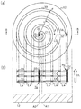
- A The top view which shows the planar structure of the high frequency spiral antenna which a plasma etching apparatus has
- B Sectional drawing which shows the cross-section of the high frequency spiral antenna.
- A The expanded sectional view which expands and shows the partial cross section structure of a high frequency spiral antenna.
- B The expanded sectional view which expands and shows the partial cross section structure of the same high frequency spiral antenna.
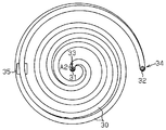
- the perspective view which shows the perspective structure of a high frequency spiral antenna.
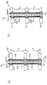
- the top view which shows the planar structure of the high frequency spiral antenna provided in the plasma etching apparatus which concerns on other embodiment.
- the top view which shows the planar structure of the high frequency spiral antenna provided in the plasma etching apparatus which concerns on other embodiment.
- FIG. 1 shows a schematic configuration of a plasma etching apparatus according to the present embodiment.
- the vacuum vessel 11 of the plasma etching apparatus 10 has a single axis A ⁇ b> 1 extending in the thickness direction of the substrate S from the substrate S accommodated in the vacuum vessel 11. It has a covered cylindrical shape that is axially symmetric.
- the top of the vacuum vessel 11 is formed of a top plate 12 that is made of quartz, which is one of dielectrics, in the shape of a disk that is also axially symmetric with respect to the first axis A1.
- a substrate stage 13 on which a substrate S that is a processing target of a plasma etching process performed therein is placed.
- a protective member 14 is provided on the outer periphery of the substrate stage 13. The protective member 14 is resistant to plasma induced in the plasma generation region 11 a and various gases used as raw materials for the plasma, and protects the substrate stage 13 from corrosion caused by these. It has been.
- the substrate stage 13 is connected to a bias high frequency power source 20 for applying a predetermined bias to the substrate S placed thereon.
- a bias matching circuit is provided between the substrate S and the bias high-frequency power source 20 to match the impedance between the gas in the plasma generation region 11a serving as a load and the transmission path from the bias high-frequency power source 20 to the substrate S. 21 is provided.
- the three-stage high-frequency spiral antenna 30 is parallel to the outer surface of the top plate 12 and circulates on different surfaces on the first axis A1. Are stacked.
- the three-stage high-frequency spiral antenna 30 is electrically connected in parallel by a columnar input terminal 33 extending in a direction parallel to the first axis A1 and an output terminal 34 extending in a direction parallel to the first axis A1. ing.
- the end of the input terminal 33 protruding from the top-stage high-frequency spiral antenna 30 is connected in series to a high-frequency power source 40, a matching circuit 41, and an input-side capacitor 42.
- a circuit and a series circuit including a DC power supply 44 and a low-pass filter 45 connected in series are connected in parallel.
- the high frequency power supply 40 outputs high frequency power for generating plasma in the plasma generation region 11a, for example, high frequency power of 13.56 MHz.
- the matching circuit 41 matches the impedance between the gas in the plasma generation region 11 a serving as a load and the transmission path from the high frequency power supply 40 to the vacuum vessel 11 including the high frequency spiral antenna 30.
- the input-side capacitor 42 is a so-called variable capacitor whose capacitance can be changed, and arbitrarily changes the capacitance in a range of 10 pF to 100 pF, for example.
- the DC power supply 44 is a power supply that can apply a DC voltage of, for example, 0 V to ⁇ 2000 kV to the input terminal 33.
- the low-pass filter 45 removes noise from the voltage output from the DC power supply 44.
- an output side capacitor 43 which is a so-called variable capacitor whose capacitance can be changed, is connected to the end of the output terminal 34 protruding from the uppermost high frequency spiral antenna 30.
- the plasma etching apparatus 10 is connected to the ground potential through the casing.
- the capacitance of the output side capacitor 43 can be arbitrarily changed within a range of, for example, 10 pF to 100 pF, similarly to the input side capacitor 42.
- the high-frequency antenna provided in the plasma processing apparatus such as the plasma etching apparatus 10 is not limited to the high-frequency spiral antenna 30 and its output terminal is connected to a predetermined reference potential such as ground. Only the potential of the input terminal of the antenna vibrates with a predetermined amplitude. Therefore, in the vicinity of the input end of the high-frequency antenna, the output end of the high-frequency antenna has a negative potential with respect to the plasma potential due to capacitive coupling between the corresponding region of the top plate and the high-frequency antenna.
- the capacitive coupling between the corresponding region of the top plate 12 and the high frequency antenna is small, it is difficult for the region to have a negative potential compared to the input end side, and the adhering matter to the region There is a possibility that deposition is not suppressed.
- the inner surface of the top plate 12 made of the dielectric is negative due to the electrons in the plasma colliding with the top plate 12 even if there is no capacitive coupling between the high frequency spiral antenna 30 and the plasma in the vacuum vessel 11.
- the high frequency spiral antenna 30 and the plasma are capacitively coupled, so that a negative potential equal to or higher than the self-bias potential is applied to the inner surface of the top plate 12.
- the input side capacitor 42 is connected to the input end of the high frequency spiral antenna 30, more precisely the input terminal 33 connected to the input end, and the output terminal 34 is connected to the other end.
- the output side capacitor 43 is connected.
- a three-stage magnetic coil 50 whose center is disposed on the first axis A1 is provided on the side surface of the vacuum vessel 11, specifically, near the top plate 12 of the cylindrical portion.
- the uppermost coil 50u which is the uppermost stage, is disposed closer to the high-frequency spiral antenna 30 in the direction of the first axis A1 than the inner surface of the top plate 12.
- the middle coil 50m which is the lower stage of the upper coil 50u, is included on the inner surface of the top, that is, on the plane on which the inner surface of the top plate 12 is located in the present embodiment.
- the lower coil 50b is disposed as a lower stage of the middle coil 50m. That is, the three-stage magnetic field coil 50 is arranged with respect to the vacuum container 11 so that the cylindrical vacuum container 11 is inserted from the inside of the lower coil 50b to the inside of the middle coil 50m.
- Each of these three coils 50u, 50m, and 50b receives a current having the same direction from the corresponding power supply unit 51u, 51m, and 51b to the upper coil 50u and the lower coil 50b, and the middle coil 50m.
- a current in the direction opposite to the current supplied to the upper coil 50u and the lower coil 50b is supplied.
- an annular zero magnetic field region ZMF is formed inside the middle coil 50m along the circumferential direction of the magnetic field coil 50, in other words, along the circumferential direction on the inner surface of the vacuum vessel 11.
- the zero magnetic field region ZMF is included in the plasma generation region 11a defined by the vacuum vessel 11 and the top plate 12, and the zero magnetic field is formed by the inner surface of the top plate 12 including the arrangement surface of the middle stage coil 50m.
- the vacuum vessel 11 is configured so as to cover the region ZMF.
- the three-stage magnetic field coil 50 and the power supply units 51u, 51m, 51b and the like that supply power to the coil are configured as an example of the magnetic field forming unit.
- the vacuum vessel 11 has a gas inlet 15 for introducing an etching gas as a plasma raw material into the plasma generation region 11a, and the gas inlet 15 is connected to the plasma etching apparatus 10 with the gas inlet 15.
- a gas supply unit 60 is connected to supply various etching gases according to the plasma etching process.
- the vacuum vessel 11 is connected to an exhaust device (not shown) for adjusting the inside of the plasma generation region 11a to a predetermined pressure.
- FIG. 2A shows the planar structure of the high-frequency spiral antenna 30 and the top plate 12 provided on a plane parallel to the high-frequency spiral antenna 30, and FIG. The cross-sectional structure is shown.
- the high-frequency spiral antenna 30 is composed of a line in which a main material such as copper is plated with nickel, and passes through the center C1 of the top plate 12 having a circular shape.
- a point parallel to the axis A1 and spaced from the first axis A1 on the second axis A2 is the center C2, and a spiral shape that circulates 3.5 times around the first axis A1 and the second axis A2 is formed. ing.
- the high frequency spiral antenna 30 is A distance between an arbitrary point P on the high frequency spiral antenna 30 and the center C2 is a separation distance r,
- the high frequency spiral antenna 30 is configured in such a manner that the distance between adjacent lines on the straight line L0 is a constant distance La.
- the input end 31 which is one end where the center C2 is located is connected to the input terminal 33 among both ends of the high-frequency spiral antenna 30.
- the output end 32 which is the other end different from the input end 31, is connected to the output terminal 34.
- the three high-frequency spiral antennas 30 have high-frequency spiral antennas 30 whose planes including the high-frequency spiral antenna 30 are parallel to each other and parallel to the second axis A2.
- the projection images projected on the top plate 12 from the 30 stacking directions DL are arranged to be the same. Therefore, the input end portion 31 and the output end portion 32 of each of the three high-frequency spiral antennas 30 are located on a straight line parallel to the stacking direction DL.
- FIG. 2B which includes the input terminal 33 or the output terminal 34 and their peripheral structure. And will be described in detail.
- 3A is an enlarged view of the region Ra
- FIG. 3B is an enlarged view of the region Rb.
- a through hole penetrating in the stacking direction DL of the antenna 30 is provided.
- Conductive screw members 33a extending in the laminating direction DL are inserted through these through holes, and the screw member 33a as an input shaft of the high frequency power has a total length, that is, in a direction to be inserted into the through holes.
- Crossing threads and thread grooves are provided.
- the screw member 33a is not limited to a screw provided with a thread and a thread groove over its entire length, but also a screw provided with a thread and a thread groove only in a region screwed with another member. Is possible.
- the input end through-holes 31a that are the through-holes of the uppermost high-frequency spiral antenna 30 and the middle-stage high-frequency spiral antenna 30 in the stacking direction DL have the same shape. And the diameter is larger than the diameter of the screw member 33a inserted in this.
- the input end through hole 31b which is the through hole of the lowermost high-frequency spiral antenna 30 in the stacking direction DL, has a smaller diameter than the input end through hole 31a, and the screw member 33a inserted therein The shape is screwable. Further, the screw member 33a is screwed into the input end through hole 31b so that the front end surface in the insertion direction of the screw member 33a and the surface facing the top plate 12 of the lowermost high frequency spiral antenna 30 coincide. .
- the input spacer 33b is inserted between the uppermost high frequency spiral antenna 30 and the middle high frequency spiral antenna 30, and between the middle high frequency spiral antenna 30 and the lowermost high frequency spiral antenna 30, respectively.
- the input spacer 33b is inserted.
- Each of the input spacers 33b has a spacer through-hole 33c that penetrates in the thickness direction and through which the screw member 33a is inserted.
- the diameter of the spacer through-hole 33c is equal to the input end through-hole 31a.
- the opening of the input end through hole 31a provided in the uppermost and middle high frequency spiral antennas 30 and the opening of the spacer through hole 33c of the input spacer 33b sandwiched therebetween are matched.
- An input spacer 33b is arranged.
- the opening of the input end through hole 31a provided in the middle high frequency spiral antenna 30 and the opening of the spacer through hole 33c of the input spacer 33b sandwiched between the middle and lowermost high frequency spiral antennas 30 coincide with each other.
- the input spacer 33b is arranged in a shape.
- the outer surface of the screw member 33a inserted into the input end through hole 31a and the spacer through hole 33c is separated from the inner surface of the input end through hole 31a by a certain distance Lc, and the outer surface of the screw member 33a.
- the spacer through hole 33c is disposed so as to be separated from the inner surface by a distance Lc.
- an input spacer 33b in which the uppermost high-frequency spiral antenna 30 is disposed directly below is provided at an end protruding from the uppermost high-frequency spiral antenna 30.
- a conductive nut 33d is screwed in a form of pressing downward.
- the distance in the stacking direction DL between the input spacers 33b is defined by the thickness Lb of the input spacer 33b in the stacking direction DL.
- the distance between the inner surface of the input end through hole 31a and the outer surface of the screw member 33a of each of the uppermost and middle high frequency spiral antennas 30 is maintained at the above-described distance Lc, and the spacer through hole 33c of each input spacer 33b is maintained.
- the distance between the inner surface and the outer surface of the screw member 33a is also maintained at the above-described distance Lc. And the position of these members is being fixed, while the input end part 31 of each high frequency spiral antenna 30 is electrically connected via each input spacer 33b.
- the positions of the high-frequency spiral antenna 30 and the input spacer 33b are fixed using a conductive nut 33d screwed to the screw member 33a, and the electrical connection between these members is maintained.
- the above-mentioned member is fixed by a nut made of a non-conductive material, or without being fixed by the nut 33d, for example, the input end through hole 31a of the uppermost high-frequency spiral antenna 30 is connected to the lowermost high-frequency spiral. It can be replaced with a configuration in which the electrical connection between the members is maintained by screwing with the screw member 33a in the same shape as the input end through hole 31b of the antenna 30.
- the position of the member is fixed by providing an engagement structure that maintains the contact state by engaging and fixing the high frequency spiral antenna 30 and the input spacer 33b sandwiched therebetween. You may do it.
- each of the output end portions 32 of the three high frequency spiral antennas 30, in other words, the end portions different from the input end portion 31 among the both end portions of each high frequency spiral antenna 30. Is basically provided with an output terminal 34 having the same configuration as the input terminal 33.
- the uppermost and middle high frequency spiral antennas 30 in the stacking direction DL have output end through holes 32a
- the lowermost high frequency spiral antenna 30 has output end through holes 32b.
- the conductive material is electrically conductive between the uppermost high frequency spiral antenna 30 and the middle high frequency spiral antenna 30, and between the middle high frequency spiral antenna 30 and the lowermost high frequency spiral antenna 30, respectively.
- a cylindrical output spacer 34b is provided, and these output spacers 34b have through holes 34c having the same diameter as the output end through holes 32a.
- a screw member 34a as an output shaft of high-frequency power connected to the ground potential through the output-side capacitor 43 and the casing of the plasma etching apparatus 10 is inserted into the output end through holes 32a and 32b and the through hole 34c. ing.
- the screw member 34a through which these members are inserted is screwed into the output end through hole 32b of the lowermost high-frequency spiral antenna 30 in the same manner as the screw member 33a of the input terminal 33.
- the nut 34d for fixing the position of these members is screwed to the screw member 34a so that the uppermost high-frequency spiral antenna 30 presses the output spacer 34b disposed immediately below the nut 34d.
- the three high-frequency spiral antennas 30 are connected to each other by the input terminal 33 and the output terminal 34 at the input end 31 and the output end 32 thereof. Moreover, both the input terminal 33 and the output terminal 34 are inserted into the input end through holes 31 a and 31 b provided in the input end 31 and the output end through holes 32 a and 32 b provided in the output end 32. In other words, screw members 33a, 34a that can be attached to and detached from these through holes 31a, 31b, 32a, 32b, and the screw members 33a, 34a are inserted, in other words, attachable to and detachable from the screw members 33a, 34a are possible.
- the input spacer 33b and the output spacer 34b are possible.
- the high frequency spiral antenna 30, the input spacer 33b, and the output spacer 34b are removed from the screw members 33a and 34a to reduce the number of the high frequency spiral antennas 30, or the input spacer 33b and the output spacer 34b are added to the screw members 33a and 34a. After insertion, a new high-frequency spiral antenna 30 can be disposed.
- the screw member 33 a inserted into the input end through holes 31 a and 31 b of the high frequency spiral antenna 30 and the high frequency spiral antenna 30.
- the input terminal 33 is configured by the input spacer 33b sandwiched between and the nut 33d screwed to the screw member 33a.
- an engaging portion that can be engaged with and detached from the end portion of the high-frequency spiral antenna 30
- a pair of input spacers 33b that are sandwiched in the stacking direction DL by the input end portion 31, and the spacer penetration of these input spacers 33b
- the input engagement portion is configured by the screw member 33a inserted through the hole 33c.
- the screw member 34 a inserted into the output end through holes 32 a and 32 b of the high frequency spiral antenna 30 and the high frequency spiral antenna 30 are provided.
- the output terminal 34 is configured by the output spacer 34b and the nut 34d screwed to the screw member 34a.
- an engaging portion that can be engaged with and detached from the end portion of the high-frequency spiral antenna 30, a pair of output spacers 34b sandwiched in the stacking direction DL by the output end portion 32, and the spacer penetration of these output spacers 34b
- An output engagement portion is constituted by the screw member 34a inserted through the hole 34c.
- the screw member 33 a electrically connected to the high frequency power supply 40 is connected to the input terminal 33 via the input end 31 of the lowermost high frequency spiral antenna 30.
- the input spacer 33b in contact with this, the input end 31 of the middle high-frequency spiral antenna 30, the input spacer 33b in contact with the input end 31 and the input end 31 of the uppermost high-frequency spiral antenna 30 are supplied with high-frequency power. Is supplied. That is, the three high frequency spiral antennas 30 are electrically connected in parallel.
- the screw member 33a When the screw member 33a is fixed by the conductive nut 33d together with the uppermost and middle high-frequency spiral antennas 30 and the input spacer 33b as in the present embodiment, the screw member 33a is supplied to the screw member 33a.
- the high frequency power is also supplied to each of the high frequency spiral antenna 30 and the input spacer 33b through the nut 33d.
- FIG. 4 shows a perspective structure of the three high frequency spiral antennas 30 stacked.
- the three high-frequency spiral antennas 30 have a columnar input terminal 33 parallel to the second axis A2 at the input end 31 and the output end 32, and a second axis A2. They are fixed to each other by parallel columnar output terminals 34.
- An auxiliary spacer 35 made of an insulating material is disposed in the middle of the line to be configured.
- Each of these auxiliary spacers 35 has a shape corresponding to the high frequency spiral antenna 30 on the surface in contact with the uppermost high frequency spiral antenna 30 and the surface in contact with the middle high frequency spiral antenna 30, and the high frequency spiral antenna 30 is fixed. Has a recessed portion.
- the auxiliary spacer 35 has the same thickness in the stacking direction DL from the bottom surface of the recess as the thickness Lb in the stacking direction DL of the input spacer 33b and the output spacer 34b of each of the input terminal 33 and the output terminal 34. It is.
- the entire high frequency spiral antenna 30 is provided.
- the gap is maintained at a distance Lb equal to the thickness of the input spacer 33b and the output spacer 34b. That is, the three high-frequency spiral antennas 30 can be prevented from contacting each other in the middle of the line, and the parallel circuit composed of the high-frequency spiral antennas 30 can be reliably maintained.
- the substrate S is first vacuumed from the carry-in port provided in the plasma etching apparatus 10. It is carried into the container 11 and placed on the substrate stage 13. Next, an etching gas is supplied from the gas supply unit 60 into the plasma generation region 11a at a flow rate corresponding to each plasma etching process.
- an etching gas is supplied from the gas supply unit 60 into the plasma generation region 11a at a flow rate corresponding to each plasma etching process.
- the inside of the plasma generation region 11a is also brought into a pressure corresponding to the conditions of the plasma etching process by the exhaust device.
- the supply of the etching gas from the gas supply unit 60 and the exhaust of the plasma generation region 11a by the exhaust device are continued during the execution of the plasma etching process. Is maintained at a predetermined pressure.
- a current in the same direction is supplied to the upper coil 50u and the lower coil 50b of the magnetic field coil 50, and a current in the opposite direction is supplied to the middle coil 50m.
- a zero magnetic field region ZMF is formed inside 11a. Accordingly, high frequency power of 13.56 MHz, for example, is supplied from the high frequency power supply 40 to the high frequency spiral antenna 30 via the matching circuit 41 and the input side capacitor 42.
- the power supplied to the high frequency spiral antenna 30 is introduced from the screw member 33a of the input terminal 33 protruding from the uppermost high frequency spiral antenna 30 in the stacking direction DL of the high frequency spiral antenna 30 as described above.
- the power is supplied from the lowermost high-frequency spiral antenna 30 toward the uppermost high-frequency spiral antenna 30 or from the nut 33 d toward the uppermost high-frequency spiral antenna 30.
- the high frequency spiral antenna 30 By supplying high frequency power to the high frequency spiral antenna 30 in this way, an induction electric field is formed in the zero magnetic field region ZMF, and plasma using etching gas as a raw material is induced.
- the plasma induced in the plasma generation region 11a and the high-frequency spiral antenna 30 are capacitively coupled through the outside air or the top plate 12 outside the plasma generation region 11a. Since the capacity of the outside air and the top plate 12 outside the plasma generation region 11a is usually much larger than the capacity of the plasma generation region 11a, each capacity between the high-frequency spiral antenna 30 and the plasma.
- the potential difference distributed to the components is the largest on the inner surface of the top plate 12. Thereby, the inner surface of the top plate 12 is in a negatively charged state, that is, a state in which a so-called negative DC bias (negative self bias) is applied.
- a direct current voltage of ⁇ 1.5 kV is applied to the high-frequency spiral antenna 30 through the low-pass filter 45 in a continuous or pulse manner.
- the voltage applied to the high frequency spiral antenna 30 is a superposition of the high frequency voltage and the DC voltage.
- the high frequency spiral antenna 30 and the plasma in the plasma generation region 11a are capacitively coupled, and the inner surface of the top plate 12 made of a dielectric is given a negative DC bias.
- the negative self-bias due to the application of the high-frequency voltage is given by the collision of electrons generated in the plasma generation region 11a, whereas the negative bias due to the application of the DC voltage is applied to the high-frequency spiral antenna 30. It is given directly by the negative DC voltage applied.
- the DC voltage applied to the high-frequency spiral antenna 30 is consumed for capacitive coupling between the plasma generated by the high-frequency power and the high-frequency spiral antenna 30, and the DC voltage is It does not contribute to plasma generation.
- the substrate S Thereafter, when the high frequency power of 13.56 MHz, for example, is supplied from the bias high frequency power supply 20 to the substrate S, a bias voltage corresponding to the high frequency power is applied to the substrate S.
- active species particularly positive ions, present in the plasma generation region 11a are drawn into the substrate S and function as an etchant.
- the predetermined region of the substrate S is etched along its vertical direction, in other words, along its thickness direction.
- the particles emitted from the constituent material of the substrate S to be processed and the configuration of the substrate S are processed.
- a cumulative amount of a product derived from a reaction between the material and the etching gas or a deviation from the etching gas increases.
- these various substances collide with the inner surface of the vacuum container 11 in accordance with the gas flow formed by the gas supply from the gas supply unit 60 and the exhaust by the exhaust device in the vacuum container 11, It comes to adhere to this.
- the deposits are difficult to deposit on the inner surface of the top corresponding to the outer periphery of the high-frequency loop antenna.
- deposits are likely to deposit on the inner surface of the top plate 12 corresponding to the other part, particularly the region inside the outer periphery of the high-frequency loop antenna.
- the deposits deposited on the top plate 12 are peeled off from the top portion depending on conditions such as the temperature during the plasma etching process performed in the vacuum vessel 11 and the internal pressure of the vacuum vessel, thereby contaminating the substrate S. There is a fear.
- the outer periphery since the high-frequency spiral antenna 30 having a spiral shape is adopted as the high-frequency antenna, the outer periphery has the same size as the high-frequency spiral antenna 30 compared with the high-frequency loop antenna.
- the region of the top plate 12 corresponding to the outer periphery of the high frequency spiral antenna 30 but also the region of the top plate 12 corresponding to the inner side of the outer periphery is set to a negative voltage with respect to the plasma in the vacuum vessel 11.
- positive ions contained in the plasma can be drawn into these regions. That is, it is possible to suppress deposition of plasma and deposits derived from the etching process using the plasma due to the collision of positive ions with the top plate 12.
- the top surface of the top plate 12 has a negative voltage derived from the high frequency power. And a negative bias derived from a direct current voltage. Therefore, the amount of positive ions attracted to the inner surface of the top plate 12 can be increased by the amount of the negative bias derived from the DC voltage in this way, and as a result, deposition of deposits on the top plate 12 can be further suppressed. It becomes like this.
- each high-frequency spiral antenna 30 has a long self-inductance and a high inductive reactance because the line length is longer than that of the loop-shaped high-frequency antenna.
- the combined inductance is the sum of the self-inductances of the individual high-frequency spiral antennas 30.
- the inductance of the plurality of high-frequency spiral antennas 30 increases.
- the combined inductance is the reciprocal of the sum of the reciprocals of the self-inductances of the individual high-frequency spiral antennas 30.
- the combined inductance is smaller than the self-inductance of the individual high-frequency spiral antennas 30. Further, as the number of the high-frequency spiral antennas 30 is increased, the degree of decrease in the combined inductance with respect to the self-inductance of the individual high-frequency spiral antennas 30 is increased. Become.
- the impedance of a transmission path from a high-frequency power source including a high-frequency antenna to a vacuum vessel is normally matched with the impedance of a vacuum vessel containing plasma.
- the high frequency power applied from the high frequency power source to the vacuum container side is prevented from being reflected as a reflected wave to the high frequency power source side, and the high frequency power that does not contribute to plasma generation is suppressed.
- the matching between the impedance of the transmission line and the impedance of the vacuum vessel is generally realized by providing a matching circuit in the previous stage of the high-frequency antenna in the transmission line.
- the matching circuit 41 is configured using an inductor or a capacitor, and has an impedance that cancels out the difference between the impedance of the transmission path and the impedance of the vacuum vessel 11.
- the inductance increases due to the adoption of the spiral high frequency spiral antenna 30, it is necessary to correct the capacitance reactance in the matching circuit 41 provided between the high frequency spiral antenna 30 and the high frequency power supply 40.
- parasitic capacitance in the high-frequency power transmission path has a great influence on impedance matching itself.
- the self-inductance of the high-frequency spiral antenna 30 as a whole can be made substantially the same as that of the loop-shaped high-frequency antenna, and the impedance of the vacuum vessel 11 Accordingly, the high frequency spiral antenna 30 can be added or removed. That is, the ratio of the decrease in the capacitive reactance due to the provision of the spiral high frequency spiral antenna 30 is also suppressed, and the influence of the parasitic capacitance of the transmission path on the impedance matching can be reduced. It becomes possible to suppress stabilization. Furthermore, the loss of electric energy that contributes to plasma induction is suppressed.
- the state of the induced plasma fluctuates due to the change in the etching processing conditions performed in the plasma etching apparatus 10 as well as the suppression of the instability of the plasma state due to impedance mismatch and the resulting loss of power.
- impedance matching is achieved by the high frequency spiral antenna 30 itself by changing the number of the high frequency spiral antennas 30. Therefore, it is possible to suppress deposits from being deposited on the top plate 12 of the vacuum vessel 11 while suppressing a decrease in versatility of the plasma etching apparatus 10.
- the high frequency spiral antenna 30 having a spiral shape is adopted as the high frequency antenna.
- the high frequency loop antenna whose outer periphery size is the same as the high frequency spiral antenna 30
- the 12 regions can also be set to a negative voltage with respect to the plasma in the vacuum vessel 11, and positive ions contained in the plasma can be drawn into these regions. That is, it is possible to suppress deposition of plasma and deposits derived from the etching process using the plasma due to the collision of positive ions with the top plate 12.
- a three-stage high frequency spiral antenna 30 was provided, and these high frequency spiral antennas 30 were connected in parallel.
- the self-inductance of the three-stage high-frequency spiral antenna 30 as a whole can be made substantially the same as that of a single high-frequency loop antenna. That is, the rate of decrease in capacitive reactance due to the provision of the high frequency spiral antenna 30 is suppressed, the influence of parasitic capacitance of the transmission path on impedance matching can be reduced, and plasma instability can be suppressed. Become. Furthermore, the loss of electric energy that contributes to plasma induction is suppressed. That is, it is possible to suppress instability of the plasma state due to impedance mismatch and power loss due to the instability.
- An output terminal 34 that engages and disengages is used.
- the high-frequency spiral antenna 30 can be added or removed.
- the state of the induced plasma fluctuates due to a change in the etching process conditions performed in the plasma etching apparatus 10, so that the transmission line and the vacuum vessel 11 are changed.
- impedance matching is achieved by the high frequency spiral antenna 30 itself by changing the number of high frequency spiral antennas 30. Therefore, it is possible to suppress a decrease in versatility of the plasma etching apparatus 10.
- the input spacer 33b and the output spacer 34b are inserted between the high-frequency spiral antennas 30. Accordingly, the distance between the pair of input end portions 31 sandwiching the input spacer 33b is determined by the thickness Lb of the input spacer 33b in the stacking direction DL, and the output spacer is determined by the thickness Lb of the output spacer 34b in the stacking direction DL. The distance between the output ends 32 sandwiching 34b, that is, the length of the transmission path for high-frequency power is determined. In addition, it is possible to form a space corresponding to the thickness Lb of the input spacer 33b and the thickness Lb of the output spacer 34b over substantially the entire space between the pair of high-frequency spiral antennas 30 adjacent in the stacking direction DL.
- the length of the transmission path of the high frequency power in each of the three high frequency spiral antennas 30 and the distance between each of the three high frequency spiral antennas 30 and the inside of the vacuum vessel 11 are the thicknesses of these input and output spacers 33b and 34b. Adjustment is possible by the length Lb. Therefore, the state of the induction magnetic field leaking into the inside of the vacuum vessel 11, and hence the state of the plasma generated by the induction magnetic field, not only the number of the high frequency spiral antennas 30, but also the thickness Lb of the input and output spacers 33b and 34b. Can also be adjusted.
- the input side capacitor 42 is connected to the input terminal 33 provided at the input end 31 of the high frequency spiral antenna 30, and the output side capacitor is connected to the output terminal 34 provided at the output end 32 of the high frequency spiral antenna 30. 43 is connected.
- a three-stage magnetic field coil 50 whose center is coaxially arranged is provided.
- the zero magnetic field region ZMF is formed by the three-stage magnetic field coil 50, so that the electrons collected along the magnetic field gradient can generate a higher density plasma than when the zero magnetic field region ZMF is not formed.
- positive ions contained in the plasma also exist at a high density. That is, the number of positive ions that can be drawn into the top plate 12 can be increased, and the frequency at which the top plate 12 is bombarded by positive ions can be increased. It becomes possible to suppress it reliably.
- a DC voltage is applied.
- the negative bias applied to the inner surface of the top plate 12 is also drawn toward the top plate 12 because the bias derived from the high frequency voltage and the bias derived from the DC voltage are superimposed.
- Positive ions can be increased. That is, as compared with the case where only the high frequency voltage is applied, the spattering on the top plate 12 is increased, and as a result, the deposition of deposits on the inner surface of the top plate 12 can be further suppressed.
- Sputtering on the inner surface of the top plate 12 can be increased by superimposing the high-frequency voltage and the DC voltage. As a result, the amount of secondary electrons emitted is increased, and the density of plasma generated in the plasma generation region 11a is also increased.
- the said embodiment can also be suitably changed and implemented as follows.
- the zero magnetic field region ZMF is formed in the vacuum vessel 11 by using the magnetic field coil 50 and the power supply units 51u, 51m, 51b for supplying current thereto, and plasma is formed along the zero magnetic field region ZMF.
- the magnetic field coil 50 and the power supply units 51u, 51m, and 51b are not provided, and plasma is generated in the vacuum chamber 11 only by supplying high frequency power from the high frequency power supply 40 to the high frequency spiral antenna 30. It may be.
- the spiral shape of the high-frequency spiral antenna 30 may be a spiral shape that develops on a hemisphere, a so-called helix shape, as well as a so-called spiral shape that develops on a single plane.
- the top plate 12 included in the vacuum vessel 11 may have a so-called dome shape in which the outer surface has a hemispherical shape instead of the planar shape as described above.
- FIG. 5 shows a planar structure in which two high-frequency spiral antennas 30 are stacked as viewed from a direction parallel to the second axis A2.
- the number of turns of the high-frequency spiral antenna 30 on the side closer to the viewpoint, in other words, the upper stage is 2.5 when the 360 ° rotation of the line is one turn, which is far from the viewpoint.
- the number of turns of the lower high-frequency spiral antenna 30 is 3.5.
- the arrangement of the three-stage high-frequency spiral antenna 30 is such that the shapes projected on the outer surface of the top plate 12 in the stacking direction DL, in other words, in the direction parallel to the second axis A2, are the same. Assumed. That is, the spiral directions of the high-frequency spiral antennas 30 are the same, and the lines are arranged so as not to cross each other when viewed from the direction of the second axis A2. With such a configuration, by providing the spiral high frequency spiral antenna 30 on the top plate 12, it is possible to make the top plate 12 have a negative potential with respect to the plasma induced in the vacuum vessel 11. Become.
- the area of the top plate 12 corresponding to the position immediately below it may be less likely to be a negative potential than the area corresponding to the position immediately below the line.
- the top plate 12 is mixed with a region where the accumulation of the deposit is suppressed and a portion where the deposition is difficult to be suppressed.
- these high frequency spiral antennas 30 may be arranged so that the lines intersect with each other when viewed from a direction parallel to the second axis A2, that is, the spiral directions are opposite to each other.
- FIG. 6 and FIG. 7 show a planar structure of a structure in which two high frequency spiral antennas 30 are stacked, as seen from the top surface, as in FIG.
- two high-frequency spiral antennas 30 having the same number of turns have opposite spiral directions, and the lines constituting these high-frequency spiral antennas 30 cross each other when viewed from above. It is said that.
- FIG. 6 and FIG. 7 show a planar structure of a structure in which two high frequency spiral antennas 30 are stacked, as seen from the top surface, as in FIG.
- two high-frequency spiral antennas 30 having the same number of turns have opposite spiral directions, and the lines constituting these high-frequency spiral antennas 30 cross each other when viewed from above. It is said that.
- FIG. 6 and FIG. 7 show a planar structure of a structure in which two high frequency spiral
- the number of turns of the two high-frequency spiral antennas 30 having different turns, more precisely, the side closer to the viewpoint, that is, the upper-stage high-frequency spiral antenna 30, is 2.5, while the viewpoint In the two high-frequency spiral antennas 30 that are 3.5 turns, the spiral direction may be changed. That is, the high-frequency spiral antenna 30 in FIG. 7 is arranged so that the direction of the spiral is opposite to each other, and the lines of the high-frequency spiral antenna 30 intersect each other when viewed from the above viewpoint. According to this configuration, (10) Another high-frequency spiral antenna 30 is also present in the space between the turns of each high-frequency spiral antenna 30, so that the area of the top plate 12 positioned immediately below the line constituting the high-frequency spiral antenna 30 is increased. become.
- the thicknesses of the two input spacers 33b provided between the high frequency spiral antennas 30 are equal to each other, and the thicknesses of the two output spacers 34b provided between the high frequency spiral antennas 30 are also equal to each other and the same as the input spacers 33b. I tried to make it thick. Not limited to this, the input spacers 33b may have different thicknesses in the stacking direction DL, and the output spacers 34b may have different thicknesses in the stacking direction DL. However, in this case, the input spacer 33b and the output spacer 34b sandwiched between the same high frequency spiral antennas 30 are, for example, between the uppermost high frequency spiral antenna 30 and the middle high frequency spiral antenna 30 in the stacking direction DL.
- the input spacer 33b and the output spacer 34b provided in the intermediate high frequency spiral antenna 30 and the lowermost high frequency spiral antenna 30 have the same thickness. It is desirable. According to this configuration, (11) The distance between each of the three high-frequency spiral antennas 30 and the inside of the vacuum vessel 11 can be adjusted in a wider range depending on the thickness of these spacers. Therefore, the state of the induction magnetic field leaking into the inside of the vacuum vessel 11 and thus the state of the plasma generated by the induction magnetic field can be adjusted in a wider range depending on the thickness of the spacer. That is, an increase in the high frequency power supplied to the high frequency antenna is more reliably suppressed.
- connection destination of the DC power supply 44 is not limited to the input terminal 33, and may be any position between the input terminal 33 and the output terminal 34 of the high-frequency spiral antenna 30, and may be a plurality of locations. Good. However, in a configuration in which a plurality of connection destinations of the DC power supply 44 are provided, the position is limited to a position where the inductive reactance is reduced by providing a plurality of high-frequency spiral antennas 30.
- the DC voltage output from the DC power supply 44 is applied to all the three-stage high-frequency spiral antennas 30.
- the present invention is not limited to this, and any one or two of the high-frequency spiral antennas 30 may be applied.
- the high frequency spiral antenna 30 to which the DC voltage is applied includes the high frequency spiral antenna 30 closest to the top plate 12, the negative potential applied to the top plate 12 by the application of the DC voltage is high. As a result, the effect of suppressing deposition of deposits on the inner peripheral surface of the top plate 12 is also increased.
- the application of the DC voltage from the DC power supply 44 to the high frequency spiral antenna 30 is continued during the supply of the high frequency power to the high frequency spiral antenna 30.
- the present invention is not limited thereto, and may be performed intermittently during the supply of high-frequency power. Note that the DC voltage application period and the application stop period can be arbitrarily set.
- the number of high-frequency spiral antennas 30 mounted on the plasma etching apparatus 10 is not limited to three, and more precisely, the conditions of processing performed in the plasma etching apparatus 10, more precisely, from the high-frequency power supply 40 including the high-frequency spiral antenna 30
- the transmission path to the vacuum vessel 11 and the impedance difference between the gas in the vacuum vessel 11 can be changed as appropriate.
- the number of input spacers 33b and output spacers 34b provided between the high-frequency spiral antennas 30 is also changed.
- the input terminal 33 and the output terminal 34 are made up of screw members 33a and 34a and input or output spacers 33b and 34b, in other words, an input engagement portion and an output engagement portion.
- the present invention is not limited thereto, and the input terminal 33 and the output terminal 34 may be configured by only the screw members 33a and 34a, respectively. That is, the input engagement portion and the output engagement portion may be configured only by the spacer. In this case, the spacer may be formed integrally with the high frequency spiral antenna 30. The point is that the terminals 33 and 34 may be configured to engage and disengage from the input end 31 or the output end 32.
- the output end 32 may be set to another reference potential instead of being grounded to the plasma etching apparatus 10.
- the end through which the second axis A ⁇ b> 2 passes is the input end 31, and the other end different from this is the output end 32.
- the end through which the second axis A ⁇ b> 2 passes may be used as an output end connected to the reference potential, and another end different from this may be used as the input end connected to the high frequency power supply 40.
- each output spacer 34b may not be conductive.
- the input side capacitor 42 is not essential. Further, the output side capacitor 43 is not essential.
- the present invention is not limited to the above-described plasma etching apparatus 10 and includes a high-frequency antenna and plasma induced by high-frequency power supplied thereto, as in the plasma etching apparatus 10 such as a plasma CVD apparatus. The present invention can also be applied to other plasma processing apparatuses used for various kinds of processing on the substrate.
Landscapes
- Chemical & Material Sciences (AREA)
- Engineering & Computer Science (AREA)
- Physics & Mathematics (AREA)
- Plasma & Fusion (AREA)
- Materials Engineering (AREA)
- General Chemical & Material Sciences (AREA)
- Chemical Kinetics & Catalysis (AREA)
- Analytical Chemistry (AREA)
- Mechanical Engineering (AREA)
- Metallurgy (AREA)
- Organic Chemistry (AREA)
- Electromagnetism (AREA)
- Spectroscopy & Molecular Physics (AREA)
- Plasma Technology (AREA)
- Drying Of Semiconductors (AREA)
Abstract
プラズマ処理装置(10)は、真空容器(11)の天部(12)上方に位置し、渦巻き形状をなす複数の高周波アンテナ(30)を含む。複数の高周波アンテナは、入力端部(31)と出力端部(32)とをそれぞれ有し、電気的に並列に接続される。各高周波アンテナの入力端部と係合可能な少なくとも1つの入力係合部(33b)が、高周波アンテナの個数を変更するために使用される。また、各高周波アンテナの出力端部と係合可能な少なくとも1つの出力係合部(34b)が、高周波アンテナの個数を変更するために使用される。複数の高周波アンテナの少なくとも1つの入力端部には1つの入力端子(33)が接続可能であり、複数の高周波アンテナの少なくとも1つの出力端部には1つの出力端子(34)が接続可能である。高周波電源(40)は整合回路(41)を介して入力端子(33)に高周波電力を供給して真空容器の内部にプラズマを生成させる。
Description
この発明は、プラズマ処理装置、例えば、基板をエッチングするエッチング装置や基板の表面に薄膜を形成する成膜装置等、高周波電力が供給された高周波アンテナにより生成されたプラズマを利用して対象物に各種の処理を施すプラズマ処理装置に関する。
従来から、例えば特許文献1に記載のように、磁束密度が「0」となるゼロ磁場領域をプラズマ中に形成するプラズマエッチング装置が知られている。このような装置によれば、プラズマ中の電子がプラズマ空間の磁場勾配に従ってゼロ磁場領域へと移動するため、ゼロ磁場領域を形成しない装置と比べてより高密度のプラズマを生成できる。上記ゼロ磁場領域を形成する方法としては、円筒状の真空容器の外周に巻かれた3段の磁場コイルのうち、上段及び下段の磁気コイルに同方向の電流が供給されて且つ、これら磁場コイルに供給された電流とは逆方向の電流が中段の磁場コイルに供給されることによって真空容器の周方向に沿ったループ状のゼロ磁場領域を同真空容器内に形成する方法が採用されている。このような方法によれば、磁場コイルに供給する電流値を調整することによりゼロ磁場領域の径が変更可能になることから、エッチング対象に対するプラズマ密度の分布が変更可能となり、ひいてはエッチング速度の均一性が向上可能にもなる。
ところで、上記プラズマエッチング装置では、エッチング処理に由来する生成物や副産物等が真空容器の内表面に付着し、真空容器内でのエッチング処理が実行される都度、このような付着物が同内表面に堆積することになる。上記エッチング処理の実行時には真空容器内の温度の変化や真空容器内の圧力の変化が繰り返されるため、こうして堆積した付着物、特に高周波アンテナから離れた部位に堆積した付着物がこれらの変化を受けて、上記内表面から剥離する虞がある。先の特許文献1に記載のように、真空容器の外周に高周波アンテナが巻かれる構成であれば、その高周波アンテナから離れた部位である真空容器の天部から付着物が剥離することとなる。こうして天部から剥離した付着物は、基板のエッチング処理面に付着してしまい、ひいては、このプラズマエッチング装置での処理を通じて製造される製品の歩留りを悪化させることになる。
そこで、上述するようなプラズマエッチング装置においては、上記真空容器の周囲に巻回された高周波アンテナを、同真空容器が有する天部上に配置させることによってこうした問題を軽減することが検討されている。このように高周波アンテナが天部に配置されれば、高周波アンテナの容量結合成分によりプラズマ電位に対する高い負の電位が天部の内表面に形成される。そして、同内表面に向けて加速されるプラズマ中の正イオンが天部に衝突するため、天部に堆積した上記付着物が正イオンによるスパッタリング効果により除去される、あるいは付着物の堆積そのものが抑制されると考えられる。
しかしながら、こうした付着物の堆積を抑制することが可能な領域を天部のより広範囲とするために、天部に占める上記高周波アンテナの配設領域を大きくする、つまり高周波アンテナを例えば渦巻き形状としてその線長を増大させると、これに比例して高周波アンテナの自己インダクタンスも増大することになる。ここで、こうした渦巻き形状の高周波アンテナに高周波電力を供給した場合は、これよりも線長が短い例えばループ形状の高周波アンテナに同一周波数の高周波電力を供給したときと比べて、上述のような自己インダクタンスの増加によって高周波アンテナの誘導リアクタンスが増加することになる。そのため、高周波アンテナと高周波電源との間に設けられた整合回路においては、該整合回路の誘導リアクタンスを低下させる補正が必要となる。その結果、整合回路における寄生容量等がインピーダンスの整合そのものに大きな影響を与えることとなり、容器内に生成されるプラズマの不安定化を招く虞がある。また、こうした高周波アンテナの延長によってループ形状の高周波アンテナと比べて高周波アンテナにおける抵抗損失も増加し、さらに上述するようなインピーダンスの不整合によっては反射損失も増加する。その結果、高周波アンテナに供給された高周波電力のうち、上記基板の処理に用いられるプラズマの誘起に寄与する割合が減少して、プラズマ密度の低下を招く虞もある。
ここで、エッチングする対象物の組成や構造が単一のものであれば、高周波アンテナの誘導リアクタンスに合わせて整合回路が再構築されることと、さらには高周波アンテナに供給される高周波電力を増加させることとによって上記問題も解決可能であろう。しかしながら、この種のプラズマエッチング装置では、それが処理する対象物の組成や構造が多岐にわたることが通常であり、それゆえに対象物の組成や構造に合わせたプラズマの密度やプラズマの電位が必要とされている。つまり、上述するような誘導リアクタンスにも広い範囲が通常必要とされている。そのため、渦巻き状の高周波アンテナを採用するにあたって、誘導リアクタンスに合わせた整合回路の再構築や、高周波電力の供給源である高周波電源の変更が対象物の種別ごとに必要になるとあっては、上記付着物の堆積を抑制することが可能になったとしても、こうした作業に多大な手間を要してしまい、汎用性を大きく欠いた装置となってしまう。
このように、真空容器の内壁、例えば天部等に付着物が堆積することの抑制と、装置における汎用性の維持とは、そのいずれかを所望の状態を満たすような条件とすれば他方の状態が担保され難くなるといういわゆるトレードオフの関係にあり、その両立が困難なものでもある。
なお、こうした問題は、上述のようなゼロ磁場領域に誘起されたプラズマを用いるプラズマエッチング装置に限らず、例えば、上記プラズマエッチング装置と同様に高周波アンテナにより誘起されたプラズマを用いる誘導結合型プラズマエッチング装置においても概ね共通して生じ得るものである。また、これらプラズマエッチング装置に限らず、上記高周波アンテナにより誘起されたプラズマを用いて基板表面に薄膜を形成するプラズマCVD装置においても、薄膜の形成成分からなるいわゆる成膜残渣が特に高周波アンテナの直下も含めた真空容器の内壁に付着物として堆積する。すなわち、高周波アンテナを備えるとともに、これに供給した高周波電力によって誘起されたプラズマを、処理対象物である基板に対する各種処理に用いる他のプラズマ処理装置においても概ね共通して生じ得るものである。
この発明は上記実情に鑑みてなされたものであり、その目的は、プラズマ処理に用いられる装置の汎用性の低下を抑制しつつ、真空容器の天部に付着物が堆積することを抑制可能なプラズマ処理装置を提供することにある。
以下、上記課題を解決するための手段及びその作用効果について記載する。
本発明の一態様は、プラズマ処理装置である。該装置は、誘電体からなる天部を有して板状の処理対象物を内部に収容する真空容器と、前記天部の上方に位置し、前記処理対象物の厚さの方向に延びる一つの軸線と平行な方向から見て当該軸線の周りを周回する渦巻き形状をなす複数の高周波アンテナであって、入力端部と出力端部とをそれぞれ有するとともに電気的に並列に接続される複数の高周波アンテナと、前記複数の高周波アンテナのそれぞれの入力端部と係合及び脱離可能であり、前記軸線と平行な方向に配列されて前記高周波アンテナの個数を増加及び減少させるための少なくとも1つの入力係合部と、前記複数の高周波アンテナの少なくとも1つの入力端部と接続可能な1つの入力端子と、前記複数の高周波アンテナのそれぞれの出力端部と係合及び脱離可能であり、前記軸線と平行な方向に配列されて前記高周波アンテナの個数を増加及び減少させるための少なくとも1つの出力係合部と、前記複数の高周波アンテナの少なくとも1つの出力端部と接続可能な1つの出力端子と、前記入力端子に電気的に接続される整合回路と、前記整合回路を介して前記入力端子に高周波電力を供給して前記真空容器の内部にプラズマを生成させる高周波電源とを備える。
本発明の一態様は、プラズマ処理装置である。該装置は、誘電体からなる天部を有して板状の処理対象物を内部に収容する真空容器と、前記天部の上方に位置し、前記処理対象物の厚さの方向に延びる一つの軸線と平行な方向から見て当該軸線の周りを周回する渦巻き形状をなす複数の高周波アンテナであって、入力端部と出力端部とをそれぞれ有するとともに電気的に並列に接続される複数の高周波アンテナと、前記複数の高周波アンテナのそれぞれの入力端部と係合及び脱離可能であり、前記軸線と平行な方向に配列されて前記高周波アンテナの個数を増加及び減少させるための少なくとも1つの入力係合部と、前記複数の高周波アンテナの少なくとも1つの入力端部と接続可能な1つの入力端子と、前記複数の高周波アンテナのそれぞれの出力端部と係合及び脱離可能であり、前記軸線と平行な方向に配列されて前記高周波アンテナの個数を増加及び減少させるための少なくとも1つの出力係合部と、前記複数の高周波アンテナの少なくとも1つの出力端部と接続可能な1つの出力端子と、前記入力端子に電気的に接続される整合回路と、前記整合回路を介して前記入力端子に高周波電力を供給して前記真空容器の内部にプラズマを生成させる高周波電源とを備える。
上記構成によれば、高周波アンテナの形状を渦巻き形状とするとともに、この渦巻き形状の高周波アンテナが複数設けられて且つ、これら複数の高周波アンテナが並列に接続されるようにしている。そのため、外周の大きさが当該高周波アンテナと同一であるループ形状の高周波アンテナと比較して、高周波アンテナの外周に対応する天部の領域はもとより、同外周よりも内側に対応する天部の領域についても、真空容器内のプラズマ電位に対してより負の電位とすることができ、これらの領域にプラズマに含有される正イオンを引き込むことができるようになる。すなわち、天部への正イオンの衝突によって、プラズマや該プラズマを用いた基板処理に由来する付着物が天部に堆積することを抑制することができるようになる。
加えて、上記構成では、複数の高周波アンテナを設けるとともに、これら高周波アンテナを並列に接続している。ここで、各々の高周波アンテナは上記ループ状の高周波アンテナと比較してその線路長が長いため、自己インダクタンスが高く、誘導リアクタンスも高い。複数の高周波アンテナを直列に接続した場合、その合成インダクタンスは、個々の高周波アンテナが有する自己インダクタンスの和であって、高周波アンテナの数を増加させる程、複数の高周波アンテナ全体としてのインダクタンス、すなわち合成インダクタンスは増大する。これに対し、複数の高周波アンテナを並列に接続した場合、その合成インダクタンスは、個々の高周波アンテナが有する自己インダクタンスの逆数の和の逆数となる。そのため、合成インダクタンスは個々の高周波アンテナが有する自己インダクタンスよりも小さくなり、しかも、高周波アンテナの数を増大する程、個々の高周波アンテナの自己インダクタンスに対する合成インダクタンスの低下度合いが大きくなる。例えば、同一の自己インダクタンスLを有する高周波アンテナを3つ並列に接続した場合、その合成インダクタンスは、L/3となる。
プラズマ処理装置では通常、高周波アンテナも含む上記高周波電源から真空容器までの伝送路のインピーダンスと、プラズマを含む真空容器のインピーダンスとの整合が図られている。これにより、高周波電源から真空容器側へ印加された高周波電力が、反射波として高周波電源側に反射すること、つまりプラズマ生成に寄与しなくなることを抑制するようにしている。また、上記2つのインピーダンスを整合させるためには一般に、伝送路における上記高周波アンテナの前段に整合回路を設けることによって実現されている。この整合回路は、インダクタやキャパシタを用いて構成されており、上記伝送路のインピーダンスと真空容器のインピーダンスとの差を相殺するようなインピーダンスを有している。しかしながら、渦巻き状の高周波アンテナが採用されることによりインダクタンスが増加するとなれば、高周波アンテナと高周波電源との間に設けられた整合回路において容量リアクタンスを低下させる補正が必要となり、高周波電力の伝送路における寄生容量等が上記2つのインピーダンスの整合そのものに大きな影響を与えることとなってしまう。
この点、上述のように複数の高周波アンテナを並列に接続すると、高周波アンテナ全体としての自己インダクタンスをループ状のアンテナとほぼ同じものとさせることができる。すなわち、上記渦巻き形状の高周波アンテナを設けたことによって高周波アンテナごとの容量リアクタンスは低下するが、並列構成の複数の高周波アンテナであれば、単一の高周波アンテナと比較して、こうした容量リアクタンスの低下が抑制されることになる。上記伝送路が有する寄生容量がインピーダンス整合に与える影響を軽減でき、プラズマの不安定化を抑制することが可能になる。さらには、プラズマを誘起するために消費される電力量が上記自己インダクタンスの増加、ひいては誘導リアクタンスの増加により損失されることを抑制できるようになる。つまり、上記2つのインピーダンスの不整合によるプラズマ状態の不安定化やそれによる電力の損失を抑制することはもとより、たとえ、当該プラズマ処理装置にて実施される処理条件の変更により誘起されるプラズマの状態が変動することによって、伝送路と真空容器の内部とのインピーダンス差が増大したとしても、高周波アンテナの個数の変更により上記2つのインピーダンスの整合が図られるようになる。それゆえにプラズマ処理に用いられる装置の汎用性の低下を抑制しつつも、真空容器の天部に付着物が堆積することを抑制することが可能となる。なお、上記渦巻き形状には、単一の平面上に展開する渦巻き形状はもとより、半球面上に展開する渦巻き形状、いわゆる螺旋形状も含まれる。
上記プラズマ処理装置の一実施例では、前記入力端部が、それを前記軸線の方向に貫通する入力端貫通孔を有し、前記出力端部が、それを前記軸線の方向に貫通する出力端貫通孔を有し、前記入力端子が、前記軸線の方向に延びる柱状をなして複数の前記入力端貫通孔に挿通される一つの入力軸と、複数の前記入力端部の間に挟入されるかたちで該入力軸が挿通される導電性の少なくとも1つの入力スペーサとを含み、該少なくとも1つの入力スペーサの各々が前記入力係合部として機能し、前記出力端子が、前記軸線の方向に延びる柱状をなして複数の前記出力端貫通孔に挿通される一つの出力軸と、複数の前記出力端部の間に挟入されるかたちで該出力軸が挿通される導電性の少なくとも1つの出力スペーサとを含み、該少なくとも1つの出力スペーサの各々が前記出力係合部として機能する。
上記構成によれば、軸線の方向における入力スペーサの厚さにより該入力スペーサを挟む一対の入力端部間の距離が定められ、さらに軸線の方向における出力スペーサの厚さにより該出力スペーサを挟む出力端部間の距離が定められるようになる。そのため、軸線の方向に隣接する一対の高周波アンテナの間に、これら入力スペーサの厚さと出力スペーサの厚さとに応じた空間を形成することが可能となる。その結果、複数の高周波アンテナのそれぞれと真空容器の内部との間隔がこれらスペーサの厚さにより調整可能となる。それゆえに、真空容器の内部に漏れ出す誘導磁場の状態、ひいては該誘導磁場により生成されるプラズマの状態が、高周波アンテナの個数だけでなく、スペーサの厚さによっても調整可能となる。
上記プラズマ処理装置の一実施例では、前記少なくとも1つの入力スペーサが、前記軸線の方向の厚さが互いに異なる複数の入力スペーサを含み、前記少なくとも1つの出力スペーサが、前記軸線の方向の厚さが互いに異なる複数の出力スペーサを含む。
上記構成によれば、複数の高周波アンテナのそれぞれと真空容器の内部との間隔がスペーサの厚さによってより広い範囲で調整可能となる。それゆえに、真空容器の内部に漏れ出す誘導磁場の状態、ひいては該誘導磁場により生成されるプラズマの状態が、スペーサの厚さによってより広い範囲で調整可能となる。つまり、高周波アンテナに供給される高周波電力の増加がより確実に抑制される。
上記プラズマ処理装置の一実施例では、前記複数の高周波アンテナの巻数が互いに異なる。
上述のように複数の高周波アンテナの巻数が互いに異なる構成によれば、複数の高周波アンテナが互いに異なるインダクタンスを有するようになるため、複数の高周波アンテナが同じインダクタンスを有する構成と比べて、合成誘導リアクタンスの範囲を拡張させることが可能となる。それゆえに合成誘導リアクタンスに合わせた整合回路の再構築、また高周波アンテナに供給される高周波電力の増加をより確実に抑制できる。
上述のように複数の高周波アンテナの巻数が互いに異なる構成によれば、複数の高周波アンテナが互いに異なるインダクタンスを有するようになるため、複数の高周波アンテナが同じインダクタンスを有する構成と比べて、合成誘導リアクタンスの範囲を拡張させることが可能となる。それゆえに合成誘導リアクタンスに合わせた整合回路の再構築、また高周波アンテナに供給される高周波電力の増加をより確実に抑制できる。
上記プラズマ処理装置の一実施例では、前記複数の高周波アンテナが前記軸線の方向から見て互いに交差する。
上述のように、渦巻き状に成形された複数の高周波アンテナを天部上に設けることにより、真空容器内に誘起されるプラズマの電位に対して該天部をより負の電位とすることが可能にはなる。ただし、複数の高周波アンテナの全てを、その渦巻きの方向が同一となるように配設した場合、それぞれの高周波アンテナを構成する線路が有する巻と巻との間隔、例えば一巻目と二巻目との間には線路が存在せず、その直下の位置に対応する天部の領域は、線路の直下の位置に対応する領域よりも低い負の電位となる虞がある。これにより、天部には、上記付着物の堆積が抑制される領域と、この堆積が抑制され難い部位とが混在することになる。
上述のように、渦巻き状に成形された複数の高周波アンテナを天部上に設けることにより、真空容器内に誘起されるプラズマの電位に対して該天部をより負の電位とすることが可能にはなる。ただし、複数の高周波アンテナの全てを、その渦巻きの方向が同一となるように配設した場合、それぞれの高周波アンテナを構成する線路が有する巻と巻との間隔、例えば一巻目と二巻目との間には線路が存在せず、その直下の位置に対応する天部の領域は、線路の直下の位置に対応する領域よりも低い負の電位となる虞がある。これにより、天部には、上記付着物の堆積が抑制される領域と、この堆積が抑制され難い部位とが混在することになる。
この点、上記構成によれば、複数の高周波アンテナが、軸線の方向から見て互いに交差するようにしているため、上述のような各高周波アンテナにおける巻と巻との間隔にも、他の高周波アンテナが存在し、高周波アンテナを構成する線路の直下に位置する天部の領域が増大するようになる。つまり、真空容器内のプラズマ電位に対して負の電位となる天部の領域、換言すれば正イオンによって衝撃される天部の領域を拡張させ、天部における上記付着物の抑制を均一化することが可能となる。
上記プラズマ処理装置の一実施例では、前記入力端子が、入力側コンデンサを介して前記高周波電源に接続され、前記出力端子が、出力側コンデンサを介して基準電位に接続される。
出力端子が所定の基準電位に直接接続される構成では、高周波アンテナの入力端子の電位のみが所定の振幅を有して振動することになる。そのため上記入力端部側においては、これに対応する天部の領域と高周波アンテナとの容量結合により該領域がプラズマ電位に対してより負の電位となるものの、上記出力端部側においては、これに対応する天部の領域と高周波アンテナとの容量結合が小さくなり、該領域が入力端部側と比較して負の電位になり難く、同領域への付着物の堆積が抑制されない虞がある。
そこで、上記構成では、上記高周波アンテナの入力端部と出力端部とに入力側コンデンサと出力側コンデンサとを接続することにより、高周波アンテナの入力側のみならず出力側の電位も所定の振幅をもって振動させ、高周波アンテナに対応する天部の領域の全体をプラズマ電位に対してより負の電位とすることができる。すなわち、高周波アンテナに対応する天部の領域の全体において付着物の堆積を抑制できるようになる。
上記プラズマ処理装置の一実施例では、前記天部の外周に渡り、中心が同軸上に配置された少なくとも3段の磁場コイルを有し、該磁場コイルの周方向に沿う環状のゼロ磁場領域を中段の磁場コイルの内側に形成する磁場形成部を更に備え、前記真空容器は、前記少なくとも3段の磁場コイルの内側に内挿されて且つ、該少なくとも3段の磁場コイルのうち最下段の磁場コイルから前記中段の磁場コイルまでに渡る筒状をなし、前記ゼロ磁場領域を内包するとともに、前記天部によって前記ゼロ磁場領域を覆うように構成されてなる。
上記構成によれば、上記複数段の磁場コイルによってゼロ磁場領域が形成されることにより、磁場勾配に沿って集まった電子によって特に高密度のプラズマが生成でき、該ゼロ磁場領域にはプラズマに含有される正イオンも高密度で存在するようになる。すなわち、天部に引き込まれ得る正イオンの数を増大させ、天部が正イオンによって衝撃される頻度を増大することが可能ともなり、ひいては、天部への付着物の堆積をより確実に抑制することができるようになる。
以下、本発明に係るプラズマ処理装置をプラズマエッチング装置として具現化した一実施の形態について、図1~図4を参照して説明する。
図1は、本実施の形態に係るプラズマエッチング装置の概略構成を示している。同図1に示されるように、プラズマエッチング装置10の真空容器11は、該真空容器11の内部に収容される基板Sから該基板Sの厚さ方向に延びる一つの第1軸線A1に対して軸対称となる有蓋円筒状をなしている。この真空容器11の天部は、同じく第1軸線A1に対して軸対称となる円板状をなして誘電体の1つである石英を構成材料とする天板12により構成されている。
図1は、本実施の形態に係るプラズマエッチング装置の概略構成を示している。同図1に示されるように、プラズマエッチング装置10の真空容器11は、該真空容器11の内部に収容される基板Sから該基板Sの厚さ方向に延びる一つの第1軸線A1に対して軸対称となる有蓋円筒状をなしている。この真空容器11の天部は、同じく第1軸線A1に対して軸対称となる円板状をなして誘電体の1つである石英を構成材料とする天板12により構成されている。
真空容器11の内部空間であるプラズマ生成領域11aには、その内部で実施されるプラズマエッチング処理の処理対象物である基板Sを載置する基板ステージ13が設けられている。この基板ステージ13の外周には、プラズマ生成領域11a内に誘起されたプラズマや該プラズマの原料となる各種ガスに耐性を有し、これらによる腐食から当該基板ステージ13を保護する保護部材14が設けられている。また、基板ステージ13には、これに載置される基板Sに所定のバイアスを印加するバイアス用高周波電源20が接続されている。なお、基板Sとバイアス用高周波電源20との間には、負荷となるプラズマ生成領域11a内のガスとバイアス用高周波電源20から基板Sまでの伝送路とのインピーダンスの整合を図るバイアス用整合回路21が設けられている。
上記真空容器11の内部から見て天板12の外側には、3段の高周波スパイラルアンテナ30が天板12の外表面と平行且つ、第1軸線A1上において互いに異なる面上を周回するように積み重ねられている。これら3段の高周波スパイラルアンテナ30は、第1軸線A1と平行な方向に延びる柱状の入力端子33と、同じく第1軸線A1と平行な方向に延びる出力端子34とによって電気的に並列に接続されている。
3段の高周波スパイラルアンテナ30のうち、最上段の高周波スパイラルアンテナ30から突出する入力端子33の端部には、直列に接続された高周波電源40と整合回路41と入力側コンデンサ42とからなる直列回路と、直列に接続された直流電源44とローパスフィルタ45とからなる直列回路とが並列に接続されている。
高周波電源40は、プラズマ生成領域11aにプラズマを生成するための高周波電力、例えば13.56MHzの高周波電力を出力する。整合回路41は、負荷となる上記プラズマ生成領域11a内のガスと、上記高周波スパイラルアンテナ30を含んで高周波電源40から真空容器11までの伝送路とのインピーダンスの整合を図る。入力側コンデンサ42は、容量の変更が可能ないわゆる可変コンデンサであって、例えば10pF~100pFの範囲で任意に静電容量を変更する。直流電源44は、例えば0V~-2000kVの直流電圧を入力端子33に印加可能な電源である。またローパスフィルタ45は、直流電源44の出力した電圧からノイズを除去する。
一方、最上段の高周波スパイラルアンテナ30から突出する出力端子34の端部には、これも容量の変更が可能ないわゆる可変コンデンサである出力側コンデンサ43が接続されるとともに、この出力側コンデンサ43は当該プラズマエッチング装置10の筐体を介して接地電位に接続されている。なお、この出力側コンデンサ43も上記入力側コンデンサ42と同様、その静電容量は、例えば10pF~100pFの範囲で任意に変更可能である。
上記高周波スパイラルアンテナ30に限らず、プラズマエッチング装置10等のプラズマ処理装置に設けられる高周波アンテナは一般に、その出力端子が接地等の所定の基準電位に接続されており、このような構成では、高周波アンテナの入力端子の電位のみが所定の振幅を有して振動することになる。そのため、高周波アンテナの入力端部付近においては、これに対応する天板の領域と高周波アンテナとの容量結合により該領域がプラズマ電位に対してより負の電位となるものの、高周波アンテナの出力端部付近においては、これに対応する天板12の領域と高周波アンテナとの容量結合が小さくなるため、該領域では入力端部側と比較して負の電位になり難く、同領域への付着物の堆積が抑制されない虞がある。なお、上記誘電体からなる天板12の内表面は、高周波スパイラルアンテナ30と真空容器11内のプラズマとの容量結合がなくとも、プラズマ内の電子が天板12に衝突することに起因する負の電位、いわゆるセルフバイアス電位を有してはいる。上述のように、高周波スパイラルアンテナ30とプラズマとが容量結合することにより、このセルフバイアス電位以上の負の電位が、天板12の内表面に付与されることになる。
この点、上記プラズマエッチング装置10によるように、高周波スパイラルアンテナ30の入力端部、正確には該入力端部に接続された入力端子33には入力側コンデンサ42を、他方、出力端子34には出力側コンデンサ43を接続するようにしている。これにより、高周波スパイラルアンテナ30の入力側のみならず出力側の電位も所定の振幅をもって振動させ、高周波スパイラルアンテナ30に対応する天板12の領域の全体を上記容量結合によって真空容器11内のプラズマに対して負の電位とすることができる。すなわち、高周波スパイラルアンテナ30に対応する天板12の領域の全体において付着物の堆積を抑制できるようになる。
上記真空容器11の側面、詳しくは筒状部の上記天板12付近には、中心が第1軸線A1上に配置された3段の磁場コイル50が設けられている。3段の磁場コイル50のうち、最上段である上段コイル50uは、上記天板12の内表面よりも第1軸線A1の方向において高周波スパイラルアンテナ30に近い位置に配置されている。また3段の磁場コイル50のうち、上段コイル50uの下段である中段コイル50mは、天部の内表面、すなわち本実施の形態においては上記天板12の内表面が位置する平面上に含まれるように配置されて、この中段コイル50mの下段として下段コイル50bが配置されている。つまり、上記筒状の真空容器11が下段コイル50bの内側から中段コイル50mの内側まで内挿されるように、真空容器11に対して3段の磁場コイル50が配置されている。
なお、これら3つのコイル50u,50m,50bのそれぞれには、対応する電力供給部51u,51m,51bから、上段コイル50uと下段コイル50bとに同一の向きを有する電流が、また、中段コイル50mに、これら上段コイル50uと下段コイル50bとに供給される電流とは逆向きの電流が供給される。これにより、磁場コイル50の周方向、換言すれば、上記真空容器11の内表面における周方向に沿って、上記中段コイル50mの内側に環状のゼロ磁場領域ZMFが形成される。すなわち、上記真空容器11と天板12とによって区画されたプラズマ生成領域11a内に上記ゼロ磁場領域ZMFが包含されるとともに、中段コイル50mの配置面を含む天板12の内表面によって上記ゼロ磁場領域ZMFが覆われるように、上記真空容器11は構成されている。このように、3段の磁場コイル50とこれに電力を供給する各電力供給部51u,51m,51b等が磁場形成部の一例として構成されている。
また、上記真空容器11は、プラズマ生成領域11a内にプラズマの原料となるエッチングガスを導入するためのガス導入口15を有しており、このガス導入口15には、当該プラズマエッチング装置10にて実施されるプラズマエッチング処理に応じた各種エッチングガスを供給するガス供給部60が接続されている。なお、同真空容器11には、プラズマ生成領域11a内を所定の圧力に調整するための図示しない排気装置が接続されてもいる。
上記高周波スパイラルアンテナ30の構造を、これが接続される入力端子33及び出力端子34の構造も含めて、図2~図4を参照して詳述する。図2(a)は、高周波スパイラルアンテナ30と、これと平行な面上に設けられた天板12の平面構造を示しており、図2(b)は、これら高周波スパイラルアンテナ30と天板12との断面構造を示している。
図2(a)に示されるように、高周波スパイラルアンテナ30は、例えば銅等の主材にニッケルめっきが施された線路からなるとともに、円形状をなす天板12の中心C1を通る上記第1軸線A1と平行且つ、該第1軸線A1から離間した第2軸線A2上の点を中心C2とし、該第1軸線A1及び第2軸線A2の周りを3.5回だけ周回する渦巻き形状をなしている。また、この高周波スパイラルアンテナ30は、
・高周波スパイラルアンテナ30上の任意の点Pと中心C2との距離を離間距離r、
・高周波スパイラルアンテナ30を含む平面上において中心C2を通る一つの直線L0と、高周波スパイラルアンテナ30上の点Pと中心C2とを結ぶ直線とのなす角度を中心角θ、
・上記離間距離rの変化率(1以上の定数)を距離変化率αとすると、
中心C2を中心とする極座標の方程式である「r=αθ」を満たすものである。また高周波スパイラルアンテナ30は、上記直線L0上において互いに隣接する線路間の距離が一定値である距離Laとなるかたちに構成されている。このような有端の渦巻き状をなす高周波スパイラルアンテナ30では、該高周波スパイラルアンテナ30の両端部のうち、中心C2が位置する一方の端部である入力端部31が上記入力端子33に接続され、この入力端部31と異なる他方の端部である出力端部32が上記出力端子34に接続されている。
・高周波スパイラルアンテナ30上の任意の点Pと中心C2との距離を離間距離r、
・高周波スパイラルアンテナ30を含む平面上において中心C2を通る一つの直線L0と、高周波スパイラルアンテナ30上の点Pと中心C2とを結ぶ直線とのなす角度を中心角θ、
・上記離間距離rの変化率(1以上の定数)を距離変化率αとすると、
中心C2を中心とする極座標の方程式である「r=αθ」を満たすものである。また高周波スパイラルアンテナ30は、上記直線L0上において互いに隣接する線路間の距離が一定値である距離Laとなるかたちに構成されている。このような有端の渦巻き状をなす高周波スパイラルアンテナ30では、該高周波スパイラルアンテナ30の両端部のうち、中心C2が位置する一方の端部である入力端部31が上記入力端子33に接続され、この入力端部31と異なる他方の端部である出力端部32が上記出力端子34に接続されている。
図2(b)に示されるように、上記3つの高周波スパイラルアンテナ30は、該高周波スパイラルアンテナ30を含む面が互いに平行に、且つ、上記第2軸線A2と平行な方向であるこれら高周波スパイラルアンテナ30の積層方向DLから上記天板12に投影された投影像が互いに同一となるように配置されている。そのため、3つの高周波スパイラルアンテナ30それぞれの入力端部31及び出力端部32は、上記積層方向DLに平行な直線上に位置することになる。
次いで、図2(b)に示される、上記入力端子33あるいは出力端子34とこれらの周辺構造も含めた領域である領域Raあるいは領域Rbについて、図3(a)、図3(b)を参照して詳細に説明する。なお、図3(a)は、領域Raを拡大して示したものであり、他方、図3(b)は、領域Rbを拡大して示したものである。
図3(a)に示されるように、3つの高周波スパイラルアンテナ30の入力端部31、換言すれば上記第2軸線A2が通る端部のそれぞれには、その厚さ方向、換言すれば高周波スパイラルアンテナ30の積層方向DLに貫通する貫通孔が設けられている。これら貫通孔には、上記積層方向DLに延びる導電性のねじ部材33aが挿通しており、この高周波電力の入力軸としてのねじ部材33aには、その全長、つまり貫通孔に挿入される方向に渡りねじ山及びねじ溝が設けられている。なお、ねじ部材33aとしては、その全長に渡りねじ山及びねじ溝が設けられたねじに限らず、他の部材と螺合される領域にのみねじ山及びねじ溝が設けられたねじ等も採用可能である。
詳述すると、これら高周波スパイラルアンテナ30のうち、積層方向DLにおける最上段の高周波スパイラルアンテナ30と中段の高周波スパイラルアンテナ30とが有する貫通孔である入力端貫通孔31aは、その形状が同一であるとともに、その直径がこれに挿入されるねじ部材33aの直径よりも大きい。これに対し、積層方向DLにおける最下段の高周波スパイラルアンテナ30が有する貫通孔である入力端貫通孔31bは、上記入力端貫通孔31aよりもその直径が小さく、これに挿入されるねじ部材33aと螺合可能な形状とされている。また、ねじ部材33aの挿入方向における先端面と最下段の高周波スパイラルアンテナ30の天板12に対向する面とが一致するように、該ねじ部材33aは入力端貫通孔31bに螺着されている。
加えて、最上段の高周波スパイラルアンテナ30と中段の高周波スパイラルアンテナ30との間、及び中段の高周波スパイラルアンテナ30と最下段の高周波スパイラルアンテナ30との間にはそれぞれ、導電性を有した円筒状の入力スペーサ33bが挟入されている。これら入力スペーサ33bのそれぞれは、その厚さ方向に貫通して上記ねじ部材33aが挿通するスペーサ貫通孔33cを有しており、該スペーサ貫通孔33cの直径は上記入力端貫通孔31aに等しい。また、最上段及び中段の高周波スパイラルアンテナ30に設けられた入力端貫通孔31aの開口と、それらの間に挟入された入力スペーサ33bのスペーサ貫通孔33cの開口とが一致するかたちに、該入力スペーサ33bが配置されている。また中段の高周波スパイラルアンテナ30に設けられた入力端貫通孔31aの開口と、中段及び最下段の高周波スパイラルアンテナ30の間に挟入された入力スペーサ33bのスペーサ貫通孔33cの開口とが一致するかたちに、該入力スペーサ33bが配置されている。そして、これら入力端貫通孔31a及びスペーサ貫通孔33cに挿入されるねじ部材33aの外表面と入力端貫通孔31aの内表面とが一定の距離Lcだけ離間し且つ、ねじ部材33aの外表面とスペーサ貫通孔33cの内表面とが同じく距離Lcだけ離間するように配置される。
さらに上記ねじ部材33aにおける積層方向DLの両端部のうち、最上段の高周波スパイラルアンテナ30から突出する端部には、該最上段の高周波スパイラルアンテナ30がそれの直下に配置された入力スペーサ33bを下方へ押圧するかたちに、導電性を有するナット33dが螺着されている。
このような構成によれば、最上段の高周波スパイラルアンテナ30と中段の高周波スパイラルアンテナ30との間における積層方向DLの距離、さらには中段の高周波スパイラルアンテナ30と最下段の高周波スパイラルアンテナ30との間における積層方向DLの距離がそれぞれ、入力スペーサ33bの積層方向DLにおける厚さLbにより規定されている。また、最上段及び中段の各高周波スパイラルアンテナ30の入力端貫通孔31aの内表面とねじ部材33aの外表面との距離が上述の距離Lcに維持され、各入力スペーサ33bのスペーサ貫通孔33cの内表面とねじ部材33aの外表面との距離が同じく上述の距離Lcに維持される。そして、各高周波スパイラルアンテナ30の入力端部31が各入力スペーサ33bを介して電気的に接続されつつ、これら部材の位置が固定されている。
なお、本実施の形態では、ねじ部材33aに螺合する導電性のナット33dを用いて高周波スパイラルアンテナ30及び入力スペーサ33bの位置を固定して、これら部材間の電気的な接続を維持することを前提としている。これに限らず、非導電性の材料からなるナットにより上記部材を固定する、あるいは、ナット33dによって固定することなく、例えば最上段の高周波スパイラルアンテナ30の入力端貫通孔31aを最下段の高周波スパイラルアンテナ30の入力端貫通孔31bと同型としてねじ部材33aと螺合することにより上記部材間の電気的な接続を維持する構成に置き換えることもできる。またあるいは、高周波スパイラルアンテナ30とその間に挟入される入力スペーサ33bとの接触面に、これらを係合固定して接触状態を維持する係合構造を設けることにより、上記部材の位置を固定するようにしてもよい。
他方、図3(b)に示されるように、3つの高周波スパイラルアンテナ30の出力端部32、換言すれば各高周波スパイラルアンテナ30の両端部のうち、上記入力端部31と異なる端部のそれぞれには、基本的には上記入力端子33と同様の構成を有した出力端子34が設けられている。
すなわち、積層方向DLにおける最上段及び中段の高周波スパイラルアンテナ30は出力端貫通孔32aを有するとともに、最下段の高周波スパイラルアンテナ30は出力端貫通孔32bを有している。また、最上段の高周波スパイラルアンテナ30と中段の高周波スパイラルアンテナ30との間、及び中段の高周波スパイラルアンテナ30と最下段の高周波スパイラルアンテナ30との間にはそれぞれ、入力スペーサ33bと同様、導電性を有した円筒状の出力スペーサ34bが設けられており、これら出力スペーサ34bは、上記出力端貫通孔32aと同径の貫通孔34cを有している。これら出力端貫通孔32a,32b及び貫通孔34cには、出力側コンデンサ43及び当該プラズマエッチング装置10の筐体を介して接地電位に接続される高周波電力の出力軸としてのねじ部材34aが挿入されている。なお、これら部材を挿通するねじ部材34aは、上記入力端子33が有するねじ部材33aと同様、最下段の高周波スパイラルアンテナ30の出力端貫通孔32bと螺合している。また、これら部材の位置を固定するナット34dは、最上段の高周波スパイラルアンテナ30がそれの直下に配置された出力スペーサ34bを下方へ押圧するかたちに、ねじ部材34aに螺着されている。
上述のように、3つの高周波スパイラルアンテナ30は、その入力端部31及び出力端部32において、入力端子33及び出力端子34によって互いに接続されている。しかも、これら入力端子33及び出力端子34はいずれも、上記入力端部31に設けられた入力端貫通孔31a,31b及び出力端部32に設けられた出力端貫通孔32a,32bに挿入された、換言すればこれら貫通孔31a,31b,32a,32bへの着脱が可能なねじ部材33a,34aと、このねじ部材33a,34aが挿通する、換言すればねじ部材33a,34aへの着脱が可能な入力スペーサ33b及び出力スペーサ34bとからなる。つまり、ねじ部材33a,34aから高周波スパイラルアンテナ30、入力スペーサ33b、及び出力スペーサ34bを取り外して高周波スパイラルアンテナ30の数を減らすこと、若しくは、ねじ部材33a,34aに入力スペーサ33b及び出力スペーサ34bを挿入した上で、新たな高周波スパイラルアンテナ30を配設することが可能となる。
このように、本実施の形態では、高周波電源40に接続される端子の一例として、高周波スパイラルアンテナ30の入力端貫通孔31a,31bに挿着されるねじ部材33aと、各高周波スパイラルアンテナ30の間に挟入れた入力スペーサ33bと、ねじ部材33aに螺着したナット33dとにより入力端子33が構成されている。また、高周波スパイラルアンテナ30の端部と係合及び脱離可能な係合部の一例として、入力端部31によって積層方向DLに挟持される一対の入力スペーサ33bと、これら入力スペーサ33bのスペーサ貫通孔33cに挿通されるねじ部材33aとにより入力係合部が構成されている。
また出力側コンデンサ43を介して接地電位に接続される端子の一例として、高周波スパイラルアンテナ30の出力端貫通孔32a,32bに挿着されるねじ部材34aと、各高周波スパイラルアンテナ30の間に設けられた出力スペーサ34bと、ねじ部材34aに螺着したナット34dとにより出力端子34が構成されている。また、高周波スパイラルアンテナ30の端部と係合及び脱離可能な係合部の一例として、出力端部32によって積層方向DLに挟持される一対の出力スペーサ34bと、これら出力スペーサ34bのスペーサ貫通孔34cに挿通されるねじ部材34aとにより出力係合部が構成されている。
そして、上記入力端子33に高周波電源40からの高周波電力が供給されると、高周波電源40と電気的に接続されたねじ部材33aから最下段の高周波スパイラルアンテナ30の入力端部31を介して、これと接触する入力スペーサ33b、中段の高周波スパイラルアンテナ30が有する入力端部31、該入力端部31と接触する入力スペーサ33b、及び最上段の高周波スパイラルアンテナ30の入力端部31へ、高周波電力が供給される。つまり、3つの高周波スパイラルアンテナ30が電気的に並列をなして接続されている。なお、本実施の形態のように、ねじ部材33aが、最上段及び中段の高周波スパイラルアンテナ30、入力スペーサ33bと共々、導電性のナット33dによって固定されている場合、ねじ部材33aに供給された高周波電力は、このナット33dを介しても高周波スパイラルアンテナ30のそれぞれや入力スペーサ33bに供給される。
図4は、積層された上記3つの高周波スパイラルアンテナ30の斜視構造を示している。同図4に示されるように、3つの高周波スパイラルアンテナ30は、その入力端部31と出力端部32にて、第2軸線A2と平行な柱状の入力端子33と、同じく第2軸線A2と平行な柱状の出力端子34とによって互いに固定されている。また、最上段の高周波スパイラルアンテナ30と中段の高周波スパイラルアンテナ30との間、及び中段の高周波スパイラルアンテナ30と最下段の高周波スパイラルアンテナ30との間であって、且つ、これら高周波スパイラルアンテナ30を構成する線路の途中には、絶縁性の材料からなる補助スペーサ35が配置されている。これら補助スペーサ35はそれぞれ、最上段の高周波スパイラルアンテナ30と接する面と、中段の高周波スパイラルアンテナ30に接する面とに、該高周波スパイラルアンテナ30に対応する形状をなして、高周波スパイラルアンテナ30が固定される凹部を有している。なお、補助スペーサ35は、上記凹部の底面からの積層方向DLの厚さが、入力端子33及び出力端子34のそれぞれが有する入力スペーサ33b及び出力スペーサ34bの同積層方向DLの厚さLbと同じである。
このように各高周波スパイラルアンテナ30間に、上記入力及び出力スペーサ33b,34bの上記厚さLbと同じ厚さを有した絶縁性の補助スペーサ35が設けられるため、各高周波スパイラルアンテナ30の全体に渡り、その間隙が入力スペーサ33bと出力スペーサ34bの厚さに等しい距離Lbに維持されるようになる。すなわち、3つの高周波スパイラルアンテナ30が、線路の途中において互いに接触することが抑制でき、各高周波スパイラルアンテナ30から構成される並列回路を確実に維持することができる。
こうしたプラズマエッチング装置10にて、処理対象である基板Sにプラズマエッチング処理が施される際には、まず、当該プラズマエッチング装置10に設けられた搬入口から基板Sが当該プラズマエッチング装置10の真空容器11内に搬入されて、上記基板ステージ13上に載置される。次いで、プラズマエッチング処理のそれぞれに応じた流量にて、上記ガス供給部60からプラズマ生成領域11a内にエッチングガスが供給される。こうして、プラズマ生成領域11a内にエッチングガスが供給されると、上記排気装置によりプラズマ生成領域11a内が、これも上記プラズマエッチング処理の条件に応じた圧力とされる。なお、上記ガス供給部60からのエッチングガスの供給と、排気装置によるプラズマ生成領域11aの排気は、プラズマエッチング処理の実施中にわたり継続されるものであり、これらの協働によってプラズマ生成領域11a内が所定の圧力に維持されている。
次に、上記磁場コイル50の上段コイル50uと下段コイル50bに同一方向の電流が、他方、中段コイル50mにこれらとは逆方向の電流が供給され、中段コイル50mの内側であってプラズマ生成領域11aの内部にゼロ磁場領域ZMFが形成される。これに伴い、高周波電源40から、例えば13.56MHzの高周波電力が整合回路41及び入力側コンデンサ42を介して高周波スパイラルアンテナ30に供給される。なお、高周波スパイラルアンテナ30に供給される電力は、上述のように、高周波スパイラルアンテナ30の積層方向DLにおける最上段の高周波スパイラルアンテナ30から突出する入力端子33のねじ部材33aから導入される。その後、最下段の高周波スパイラルアンテナ30から最上段の高周波スパイラルアンテナ30に向かって、あるいはナット33dから最上段の高周波スパイラルアンテナ30に向かって供給される。こうして高周波スパイラルアンテナ30に高周波電力が供給されることにより、上記ゼロ磁場領域ZMFに誘導電場が形成され、エッチングガスを原料とするプラズマが誘起される。
このとき、プラズマ生成領域11a内に誘起されたプラズマと高周波スパイラルアンテナ30とが該プラズマ生成領域11aの外側である外気や天板12を介して容量的に結合する。上記プラズマ生成領域11aの外側である外気や天板12が有する容量とは通常、プラズマ生成領域11aが有する容量よりも非常に大きいものであるため、高周波スパイラルアンテナ30とプラズマとの間の各容量成分に配分される電位差は、上記天板12の内表面において最も大きくなる。これにより、天板12の内表面は、負に帯電した状態、いわゆる負の直流バイアス(負のセルフバイアス)を与えられた状態となる。
また、上記高周波スパイラルアンテナ30には、高周波電源40から供給される高周波電力に加え、直流電源44から例えば-1.5kVの直流電圧がローパスフィルタ45を介して連続乃至はパルス的に印加されてもいる。つまり、高周波スパイラルアンテナ30に印加される電圧とは、高周波電圧と直流電圧とが重畳されたものとなる。こうした直流電圧の印加によっても、高周波スパイラルアンテナ30とプラズマ生成領域11a内のプラズマとが容量的に結合し、誘電体からなる天板12の内表面は負の直流バイアスを与えられることになる。なお、高周波電圧の印加による負のセルフバイアスが、プラズマ生成領域11a内に生成された電子の衝突により与えられるものであるのに対し、直流電圧の印加による負のバイアスは、高周波スパイラルアンテナ30に印加された負の直流電圧によって直接的に与えられるものである。また、高周波スパイラルアンテナ30に印加された直流電圧は、上述のように、あくまで高周波電力によって生成されたプラズマと高周波スパイラルアンテナ30との容量的な結合に消費されるものであり、該直流電圧はプラズマの生成には寄与しない。
その後、上記バイアス用高周波電源20から、例えば13.56MHzの高周波電力が基板Sに供給されることにより、この高周波電力に応じたバイアス電圧が該基板Sに印加されることとなる。この基板Sに印加されたバイアス電圧によって、プラズマ生成領域11a内に存在する活性種、特に正イオンが基板Sに引き込まれてエッチャントとして機能するようになる。こうして、基板Sの所定領域がその垂直方向、換言すればその厚さ方向に沿ってエッチングされる。
ここで、上述のような基板Sに対するプラズマエッチング処理が実施されると、該プラズマエッチング処理が進行するに従い、処理対象である上記基板Sの構成材料から放出された粒子や、同基板Sの構成材料とエッチングガスとの反応に由来する生成物、あるいは、エッチングガスからの乖離物等の累積量が増大する。しかも、これら各種物質は、上記真空容器11内において、上記ガス供給部60からのガス供給と、上記排気装置による排気とによって形成されるガスの流れに従って該真空容器11の内表面に衝突し、これに付着するようになる。上述のように、ループ状の高周波アンテナが天部の外表面に配置される従来の構成においては、この高周波ループアンテナの外周に対応する天部の内表面には上記付着物が堆積し難いものの、それ以外の部位、特に高周波ループアンテナの外周よりも内側の領域に対応する天板12の内表面には付着物が堆積しやすい。しかも、この天板12に堆積した付着物は、真空容器11内で実施されるプラズマエッチング処理時の温度や、真空容器の内圧等の条件によっては天部から剥離して、基板Sを汚染する虞がある。
この点、本実施の形態では、高周波アンテナとして、渦巻き形状である高周波スパイラルアンテナ30を採用するようにしているため、外周の大きさが当該高周波スパイラルアンテナ30と同一である高周波ループアンテナと比較して、高周波スパイラルアンテナ30の外周に対応する天板12の領域はもとより、同外周よりも内側に対応する天板12の領域についても、真空容器11内のプラズマに対して負の電圧とすることができ、これらの領域にプラズマに含有される正イオンを引き込むことができるようになる。すなわち、天板12への正イオンの衝突によって、プラズマや該プラズマを用いたエッチング処理に由来する付着物が天板12に堆積することを抑制することができるようになる。
しかも、本実施の形態においては、高周波スパイラルアンテナ30への高周波電力の供給とともに、直流電圧を印加するようにもしていることから、上記天板12の内表面には、高周波電力に由来する負のバイアスと、直流電圧に由来する負のバイアスとが与えられることになる。よって、こうして直流電圧に由来する負のバイアスが与えられる分だけ、天板12の内表面への正イオンの引き込みを増やし、ひいては、天板12への付着物の堆積をより抑制することができるようになる。
また、こうして天板12の内表面に正イオンが引き込まれ、該内表面がスパッタされることにより、付着物や天板12の形成材料がスパッタ粒子としてプラズマ生成領域11a内に放出される際には、いわゆる二次電子も放出される。こうした二次電子は、プラズマ生成領域11a内に供給されるエッチングガスの分子に衝突してこれをプラズマ化する反応に寄与する。そのため、上述したような天板12のスパッタ反応によって、プラズマ生成領域11a内に生成されるプラズマの密度を増大させることができるようもなる。なお、こうしたプラズマ密度の増大効果も、高周波スパイラルアンテナ30への印加電圧として高周波電圧に直流電圧を重畳した場合の方がより大きくなる。
しかしながら、各々の高周波スパイラルアンテナ30は、上記ループ状の高周波アンテナと比較してその線路長が長いために自己インダクタンスが高く、誘導リアクタンスも高い。例えば、こうした高周波スパイラルアンテナ30を複数、且つ直列に当該プラズマエッチング装置10に搭載した場合、その合成インダクタンスは、個々の高周波スパイラルアンテナ30が有する自己インダクタンスの和であって、高周波スパイラルアンテナ30の数を増加させる程、複数の高周波スパイラルアンテナ30全体としてのインダクタンス、すなわち合成インダクタンスは増大する。これに対し、複数の高周波スパイラルアンテナ30を並列に接続した場合、その合成インダクタンスは、個々の高周波スパイラルアンテナ30が有する自己インダクタンスの逆数の和の逆数となる。そのため、合成インダクタンスは個々の高周波スパイラルアンテナ30が有する自己インダクタンスよりも小さくなり、しかも、高周波スパイラルアンテナ30の数を増大する程、個々の高周波スパイラルアンテナ30の自己インダクタンスに対する合成インダクタンスの低下度合いが大きくなる。
プラズマ処理装置では通常、高周波アンテナも含む高周波電源から真空容器までの伝送路のインピーダンスと、プラズマを含む真空容器のインピーダンスとの整合が図られている。これにより、高周波電源から真空容器側へ印加された高周波電力が、反射波として高周波電源側に反射することを抑制し、プラズマ生成に寄与しない高周波電力を抑制するようにしている。また、これら伝送路のインピーダンスと真空容器のインピーダンスとの整合は一般に、伝送路における上記高周波アンテナの前段に整合回路を設けることによって実現されている。上記整合回路41は、インダクタやキャパシタを用いて構成されており、伝送路のインピーダンスと真空容器11のインピーダンスとの差を相殺するようなインピーダンスを有している。しかしながら、渦巻き状の高周波スパイラルアンテナ30が採用されることによりインダクタンスが増加するとなれば、高周波スパイラルアンテナ30と高周波電源40との間に設けられた整合回路41において容量リアクタンスを低下させる補正が必要となり、高周波電力の伝送路における寄生容量等がインピーダンスの整合そのものに大きな影響を与えることとなってしまう。
この点、上述のように3つの高周波スパイラルアンテナ30を並列に接続すると、高周波スパイラルアンテナ30全体としての自己インダクタンスをループ状の高周波アンテナとほぼ同じものとさせることができるとともに、真空容器11のインピーダンスに応じて、高周波スパイラルアンテナ30の増設及び減設が可能である。すなわち、上記渦巻き形状の高周波スパイラルアンテナ30を設けたことに伴う容量リアクタンスの低下も、その割合が抑制されることとなり、伝送路が有する寄生容量がインピーダンス整合に与える影響を軽減でき、プラズマの不安定化を抑制することが可能になる。さらには、プラズマの誘起に寄与する電力量の損失が抑制されることとなる。つまり、インピーダンスの不整合によるプラズマ状態の不安定化やそれによる電力の損失を抑制することはもとより、たとえ、当該プラズマエッチング装置10にて実施されるエッチング処理条件の変更により誘起プラズマの状態が変動することによって、伝送路と真空容器11の内部とのインピーダンス差が増大したとしても、高周波スパイラルアンテナ30の個数の変更により高周波スパイラルアンテナ30そのものによってインピーダンスの整合が図られるようになる。それゆえにプラズマエッチング装置10の汎用性の低下を抑制しつつも、真空容器11の天板12に付着物が堆積することを抑制することが可能となる。
以上、本実施の形態に係るプラズマ処理装置によれば、以下に列挙する効果が得られるようになる。
(1)高周波アンテナとして、渦巻き形状である高周波スパイラルアンテナ30を採用するようにした。これにより、外周の大きさが当該高周波スパイラルアンテナ30と同一である高周波ループアンテナと比較して、高周波アンテナの外周に対応する天板12の領域はもとより、同外周よりも内側に対応する天板12の領域についても、真空容器11内のプラズマに対して負の電圧とすることができ、これらの領域にプラズマに含有される正イオンを引き込むことができるようになる。すなわち、天板12への正イオンの衝突によって、プラズマや該プラズマを用いたエッチング処理に由来する付着物が天板12に堆積することを抑制することができるようになる。
(1)高周波アンテナとして、渦巻き形状である高周波スパイラルアンテナ30を採用するようにした。これにより、外周の大きさが当該高周波スパイラルアンテナ30と同一である高周波ループアンテナと比較して、高周波アンテナの外周に対応する天板12の領域はもとより、同外周よりも内側に対応する天板12の領域についても、真空容器11内のプラズマに対して負の電圧とすることができ、これらの領域にプラズマに含有される正イオンを引き込むことができるようになる。すなわち、天板12への正イオンの衝突によって、プラズマや該プラズマを用いたエッチング処理に由来する付着物が天板12に堆積することを抑制することができるようになる。
(2)3段の高周波スパイラルアンテナ30を設けるとともに、これら高周波スパイラルアンテナ30を並列に接続するようにした。これにより、3段の高周波スパイラルアンテナ30全体としての自己インダクタンスを一巻の高周波ループアンテナとほぼ同じものとさせることができる。すなわち、高周波スパイラルアンテナ30を設けたことに伴う容量リアクタンスの低下割合が抑制されて、伝送路が有する寄生容量がインピーダンス整合に与える影響を軽減でき、プラズマの不安定化を抑制することが可能になる。さらには、プラズマの誘起に寄与する電力量の損失が抑制されることとなる。つまり、インピーダンスの不整合によるプラズマ状態の不安定化やそれによる電力の損失を抑制できる。
(3)3段の高周波スパイラルアンテナ30を互いに固定するに際し、高周波スパイラルアンテナ30それぞれの入力端部31と係合及び脱離する入力端子33と、該高周波スパイラルアンテナ30それぞれの出力端部32と係合及び脱離する出力端子34とを用いるようにした。これにより、高周波スパイラルアンテナ30の増設及び減設が可能となり、たとえ、当該プラズマエッチング装置10にて実施されるエッチング処理条件の変更により誘起プラズマの状態が変動することによって、伝送路と真空容器11の内部とのインピーダンス差が増大したとしても、高周波スパイラルアンテナ30の個数の変更により高周波スパイラルアンテナ30そのものによってインピーダンスの整合が図られるようになる。それゆえにプラズマエッチング装置10の汎用性の低下を抑制することが可能となる。
(4)高周波スパイラルアンテナ30間に入力スペーサ33b及び出力スペーサ34bを挟入するようにした。これにより、積層方向DLにおける入力スペーサ33bの厚さLbにより該入力スペーサ33bを挟む一対の入力端部31間の距離が定められ、さらに積層方向DLにおける出力スペーサ34bの厚さLbにより該出力スペーサ34bを挟む出力端部32間の距離、すなわち高周波電力の伝送路の長さが定められるようになる。そのうえ、積層方向DLに隣接する一対の高周波スパイラルアンテナ30の間の略全体にわたり、これら入力スペーサ33bの厚さLbと出力スペーサ34bの厚さLbに応じた空間を形成することが可能となる。その結果、3つの高周波スパイラルアンテナ30のそれぞれにおける高周波電力の伝送路の長さ、及び3つの高周波スパイラルアンテナ30のそれぞれと真空容器11の内部との間隔がこれら入力及び出力スペーサ33b,34bの厚さLbにより調整可能となる。それゆえに、真空容器11の内部に漏れ出す誘導磁場の状態、ひいては該誘導磁場により生成されるプラズマの状態が、高周波スパイラルアンテナ30の個数だけでなく、入力及び出力スペーサ33b,34bの厚さLbによっても調整可能となる。
(5)高周波スパイラルアンテナ30の入力端部31に設けられた入力端子33に入力側コンデンサ42を接続するとともに、該高周波スパイラルアンテナ30の出力端部32に設けられた出力端子34に出力側コンデンサ43を接続するようにした。これにより、高周波スパイラルアンテナ30の入力側のみならず出力側の電位も所定の振幅をもって振動させ、高周波スパイラルアンテナ30に対応する天板12の領域の全体をプラズマに対して負の電位とすることができる。すなわち、高周波スパイラルアンテナ30に対応する天板12の領域の全体において付着物の堆積を抑制できるようになる。
(6)真空容器11の側面における天板12付近に、中心が同軸上に配置された3段の磁場コイル50を設けるようにした。これにより、3段の磁場コイル50によってゼロ磁場領域ZMFが形成されることにより、磁場勾配に沿って集まった電子によって、ゼロ磁場領域ZMFを形成しない場合よりも高密度のプラズマが生成でき、該ゼロ磁場領域ZMFにはプラズマに含有される正イオンも高密度で存在するようになる。すなわち、天板12に引き込まれ得る正イオンの数を増大させ、天板12が正イオンによって衝撃される頻度を増大することが可能ともなり、ひいては、天板12への付着物の堆積をより確実に抑制することができるようになる。
(7)高周波スパイラルアンテナ30には、高周波電力、換言すれば高周波電圧を印加するのに加え、直流電圧を印加するようにした。これにより、上記天板12の内表面に与えられる負のバイアスも、高周波電圧に由来するバイアスと直流電圧に由来するバイアスとが重畳されたものとなることから、天板12に向かって引き込まれる正イオンを増加させることができる。つまり、高周波電圧のみを印加した場合と比較して、天板12に対するスパッタを増加させ、ひいては、該天板12の内表面への付着物の堆積がより抑制できるようになる。
(8)また、高周波電圧と直流電圧とを重畳することにより、天板12の内表面に対するスパッタを増加させることができる。これにより、放出される二次電子の量が増大され、プラズマ生成領域11a内に生成されるプラズマの密度も増大されるようになる。
なお、上記実施の形態は、以下のように適宜変更して実施することもできる。
・磁場コイル50とこれに電流を供給する電力供給部51u,51m,51bを用いて、上記真空容器11内にゼロ磁場領域ZMFを形成し、これに沿ったプラズマを形成するようにした。これに限らず、磁場コイル50と電力供給部51u,51m,51bとを有さず、高周波電源40から高周波スパイラルアンテナ30に高周波電力を供給することのみによって真空容器11内にプラズマを生成するようにしてもよい。
・磁場コイル50とこれに電流を供給する電力供給部51u,51m,51bを用いて、上記真空容器11内にゼロ磁場領域ZMFを形成し、これに沿ったプラズマを形成するようにした。これに限らず、磁場コイル50と電力供給部51u,51m,51bとを有さず、高周波電源40から高周波スパイラルアンテナ30に高周波電力を供給することのみによって真空容器11内にプラズマを生成するようにしてもよい。
・高周波スパイラルアンテナ30の渦巻き形状には、単一の平面上に展開する渦巻き形状であるいわゆるスパイラル形状はもとより、半球面上に展開する渦巻き形状である螺旋形状、いわゆるヘリックス形状であってもよい。この場合、真空容器11が有する天板12は、上述のような平面形状ではなく、外表面が半球面状となる、いわゆるドーム形状であってもよい。
・3つの高周波スパイラルアンテナ30は、その全てが同一の形状であるようにした。これに限らず、3つの高周波スパイラルアンテナ30は、その線長が互いに異なる、換言すれば渦巻きの巻数が互いに異なるようにしてもよい。例えば、図5は2つの高周波スパイラルアンテナ30が積層されたものを、第2軸線A2と平行な方向から見た平面構造を示している。同図5に示されるように、視点に近い側の、換言すれば上段の高周波スパイラルアンテナ30の巻数は、線路の360°回転を1巻としたとき、2.5巻であり、視点から遠い側の、換言すれば下段の高周波スパイラルアンテナ30の巻数は3.5巻である。こうした構成により、
(9)複数の高周波スパイラルアンテナ30の巻数が互いに異なる構成によれば、複数の高周波スパイラルアンテナ30が互いに異なるインダクタンスを有するようになるため、複数の高周波スパイラルアンテナ30が同じインダクタンスを有する構成と比べて、合成誘導リアクタンスの範囲を拡張させることが可能となる。それゆえに合成誘導リアクタンスに合わせた整合回路の再構築、また高周波スパイラルアンテナ30に供給される高周波電力の増加をより確実に抑制できる。
(9)複数の高周波スパイラルアンテナ30の巻数が互いに異なる構成によれば、複数の高周波スパイラルアンテナ30が互いに異なるインダクタンスを有するようになるため、複数の高周波スパイラルアンテナ30が同じインダクタンスを有する構成と比べて、合成誘導リアクタンスの範囲を拡張させることが可能となる。それゆえに合成誘導リアクタンスに合わせた整合回路の再構築、また高周波スパイラルアンテナ30に供給される高周波電力の増加をより確実に抑制できる。
といった効果が得られるようになる。
・3段の高周波スパイラルアンテナ30の配置は、これらを天板12の外表面に対して上記積層方向DL、換言すれば第2軸線A2と平行な方向に投影した形状が互いに同一となる配置を前提とした。すなわち、高周波スパイラルアンテナ30それぞれの渦巻きの方向が同一であって、上記第2軸線A2の方向から見て線路が互いに交差しない配置とされるようにした。こうした構成であれば、渦巻き状の高周波スパイラルアンテナ30を天板12上に設けることにより、真空容器11内に誘起されるプラズマに対して該天板12を負の電位とすることが可能にはなる。
・3段の高周波スパイラルアンテナ30の配置は、これらを天板12の外表面に対して上記積層方向DL、換言すれば第2軸線A2と平行な方向に投影した形状が互いに同一となる配置を前提とした。すなわち、高周波スパイラルアンテナ30それぞれの渦巻きの方向が同一であって、上記第2軸線A2の方向から見て線路が互いに交差しない配置とされるようにした。こうした構成であれば、渦巻き状の高周波スパイラルアンテナ30を天板12上に設けることにより、真空容器11内に誘起されるプラズマに対して該天板12を負の電位とすることが可能にはなる。
ただし、高周波スパイラルアンテナ30の全てを、その渦巻きの方向が同一となるように配設した場合、それぞれの高周波スパイラルアンテナ30を構成する線路が有する巻と巻との間隔、例えば一巻目と二巻目との間には線路が存在せず、その直下の位置に対応する天板12の領域は、線路の直下の位置に対応する領域よりも負の電位になり難くなる虞がある。これにより、天板12には、上記付着物の堆積が抑制される領域と、この堆積が抑制され難い部位とが混在することになる。
そこで、これら高周波スパイラルアンテナ30は、第2軸線A2と平行な方向から見て線路が交差するように、すなわち互いに渦巻きの方向が逆となる配置としてもよい。例えば、図6及び図7は、先の図5と同様、2つの高周波スパイラルアンテナ30が積層されたものを、その上面から見た平面構造を示している。図6に示されるように、巻数が同一である2つの高周波スパイラルアンテナ30は、その渦巻きの方向が互いに逆であり、これら高周波スパイラルアンテナ30を構成する線路が、上面視した場合に交差する配置とされている。また、図7に示されるように、巻数が異なる2つの高周波スパイラルアンテナ30、より正確には、視点に近い側、つまり上段の高周波スパイラルアンテナ30の巻数は2.5巻であり、他方、視点から遠い側、つまり下段の高周波スパイラルアンテナ30の巻数は3.5巻である2つの高周波スパイラルアンテナ30において、その渦巻き方向を変更してもよい。つまり、図7の高周波スパイラルアンテナ30は、互いにその渦巻きの方向が逆となるように配置されており、上記視点から見て高周波スパイラルアンテナ30の線路同士が交差している。こうした構成によれば、
(10)各高周波スパイラルアンテナ30における巻と巻との間隔にも、他の高周波スパイラルアンテナ30が存在し、高周波スパイラルアンテナ30を構成する線路の直下に位置する天板12の領域が増大するようになる。つまり、真空容器11内のプラズマに対して負の電位となる天板12の領域、換言すれば正イオンによって衝撃される天板12の領域を拡張させ、天板12における上記付着物の抑制を均一化することが可能となる。
(10)各高周波スパイラルアンテナ30における巻と巻との間隔にも、他の高周波スパイラルアンテナ30が存在し、高周波スパイラルアンテナ30を構成する線路の直下に位置する天板12の領域が増大するようになる。つまり、真空容器11内のプラズマに対して負の電位となる天板12の領域、換言すれば正イオンによって衝撃される天板12の領域を拡張させ、天板12における上記付着物の抑制を均一化することが可能となる。
・高周波スパイラルアンテナ30間に設けられる2つの入力スペーサ33bの厚さを互いに等しくするとともに、同じく高周波スパイラルアンテナ30間に設けられる2つの出力スペーサ34bの厚さも互いに等しく、且つ入力スペーサ33bと同一の厚さとするようにした。これに限らず、入力スペーサ33bは積層方向DLにおいて互いに異なる厚さを有するようにしてもよく、また、出力スペーサ34bも積層方向DLにおいて互いに異なる厚さを有するようにしてもよい。ただしこの場合、同一の高周波スパイラルアンテナ30間に挟入される入力スペーサ33bと出力スペーサ34bとは、例えば、上記積層方向DLにおける最上段の高周波スパイラルアンテナ30と中段の高周波スパイラルアンテナ30との間に設けられる入力スペーサ33bと出力スペーサ34bとは、また、中段の高周波スパイラルアンテナ30と最下段の高周波スパイラルアンテナ30との間に設けられる入力スペーサ33bと出力スペーサ34bとは、同一の厚さとすることが望ましい。こうした構成によれば、
(11)3つの高周波スパイラルアンテナ30のそれぞれと真空容器11の内部との間隔がこれらスペーサの厚さによってより広い範囲で調整可能となる。それゆえに、真空容器11の内部に漏れ出す誘導磁場の状態、ひいては該誘導磁場により生成されるプラズマの状態が、スペーサの厚さによってより広い範囲で調整可能となる。つまり、高周波アンテナに供給される高周波電力の増加がより確実に抑制される。
(11)3つの高周波スパイラルアンテナ30のそれぞれと真空容器11の内部との間隔がこれらスペーサの厚さによってより広い範囲で調整可能となる。それゆえに、真空容器11の内部に漏れ出す誘導磁場の状態、ひいては該誘導磁場により生成されるプラズマの状態が、スペーサの厚さによってより広い範囲で調整可能となる。つまり、高周波アンテナに供給される高周波電力の増加がより確実に抑制される。
といった効果が得られるようになる。
・直流電源44から出力される電圧にノイズが含まれる場合であっても、プラズマ生成領域11aに生成されるプラズマが十分に安定するのであれば、直流電源44に接続されるローパスフィルタ45は割愛されてもよい。
・直流電源44から出力される電圧にノイズが含まれる場合であっても、プラズマ生成領域11aに生成されるプラズマが十分に安定するのであれば、直流電源44に接続されるローパスフィルタ45は割愛されてもよい。
・直流電源44の接続先は、入力端子33に限らず、高周波スパイラルアンテナ30の入力端子33と出力端子34との間のいずれかの位置であってもよく、さらには複数箇所であってもよい。ただし、直流電源44の接続先が複数設けられる構成では、高周波スパイラルアンテナ30を複数設けたことにより誘導リアクタンスが低下するような位置に限られる。
・直流電源44から出力された直流電圧が、3段の高周波スパイラルアンテナ30の全てに印加されるようにした。これに限らず、これら高周波スパイラルアンテナ30のうち、いずれか1つあるいは2つに印加されるようにしてもよい。この場合、直流電圧が印加される高周波スパイラルアンテナ30には、天板12に最も近い高周波スパイラルアンテナ30が含まれていると、直流電圧の印加により天板12に付与される負の電位が高くなり、ひいては、天板12の内周面への付着物の堆積を抑制する効果も大きくなる。
・直流電源44から高周波スパイラルアンテナ30への直流電圧の印加は、該高周波スパイラルアンテナ30への高周波電力の供給中に渡り継続されるようにした。これに限らず、高周波電力の供給中、間欠的に実施されるようにしてもよい。なお、直流電圧の印加期間や印加停止の期間は任意に設定可能である。
・プラズマエッチング装置10に搭載される高周波スパイラルアンテナ30は3つに限らず、当該プラズマエッチング装置10にて実施される処理の条件、より正確には、高周波スパイラルアンテナ30を含んだ高周波電源40から真空容器11までの伝送路と、真空容器11内のガスとのインピーダンス差等に応じて適宜変更可能である。なお、高周波スパイラルアンテナ30の数を変更した場合、高周波スパイラルアンテナ30間に設けられる入力スペーサ33b、及び出力スペーサ34bの数にも変更が伴うことになる。
・入力端子33と出力端子34は、ねじ部材33a,34aと入力あるいは出力スペーサ33b,34bとから、換言すれば入力係合部と出力係合部とからなるようにした。これに限らず、入力端子33と出力端子34はそれぞれねじ部材33a,34aのみからなる構成でもよい。つまり、入力係合部及び出力係合部がスペーサのみからなる構成でもよい。この場合、スペーサは高周波スパイラルアンテナ30と一体形成される構成としてもよい。要は、それぞれの端子33,34が入力端部31あるいは出力端部32に対して係合及び脱離する構成であればよい。
・出力端部32はプラズマエッチング装置10に接地されるのではなく、他の基準電位とされるようにしてもよい。
・高周波スパイラルアンテナ30の両端のうち、第2軸線A2が通る端部を入力端部31とし、これとは異なる他の端部を出力端部32とした。これに限らず、第2軸線A2が通る端部を基準電位に接続される出力端部とし、これとは異なる他の端部を高周波電源40に接続される入力端部としてもよい。
・高周波スパイラルアンテナ30の両端のうち、第2軸線A2が通る端部を入力端部31とし、これとは異なる他の端部を出力端部32とした。これに限らず、第2軸線A2が通る端部を基準電位に接続される出力端部とし、これとは異なる他の端部を高周波電源40に接続される入力端部としてもよい。
・各高周波スパイラルアンテナ30の入力端部31が導電性のねじ部材33aに螺合している場合、ねじ部材33aを介して全てのアンテナ30が電気的に接続されるため、各入力スペーサ33bは導電性でなくてもよい。同様に、各高周波スパイラルアンテナ30の出力端部32が導電性のねじ部材34aに螺合している場合、各出力スペーサ34bは導電性でなくてもよい。
・入力側コンデンサ42は必須ではない。また、出力側コンデンサ43は必須ではない。
・本発明は、上記プラズマエッチング装置10に限らず、例えばプラズマCVD装置等、プラズマエッチング装置10と同様に、高周波アンテナを備えるとともに、これに供給した高周波電力によって誘起されたプラズマを、処理対象物である基板に対する各種処理に用いる他のプラズマ処理装置にも適用可能である。
・本発明は、上記プラズマエッチング装置10に限らず、例えばプラズマCVD装置等、プラズマエッチング装置10と同様に、高周波アンテナを備えるとともに、これに供給した高周波電力によって誘起されたプラズマを、処理対象物である基板に対する各種処理に用いる他のプラズマ処理装置にも適用可能である。
Claims (7)
- プラズマ処理装置であって、
誘電体からなる天部を有して板状の処理対象物を内部に収容する真空容器と、
前記天部の上方に位置し、前記処理対象物の厚さ方向に延びる一つの軸線と平行な方向から見て当該軸線の周りを周回する渦巻き形状をなす複数の高周波アンテナであって、入力端部と出力端部とをそれぞれ有するとともに電気的に並列に接続される複数の高周波アンテナと、
前記複数の高周波アンテナのそれぞれの入力端部と係合及び脱離可能であり、前記軸線と平行な方向に配列されて前記高周波アンテナの個数を増加及び減少させるための少なくとも1つの入力係合部と、
前記複数の高周波アンテナの少なくとも1つの入力端部と接続可能な1つの入力端子と、
前記複数の高周波アンテナのそれぞれの出力端部と係合及び脱離可能であり、前記軸線と平行な方向に配列されて前記高周波アンテナの個数を増加及び減少させるための少なくとも1つの出力係合部と、
前記複数の高周波アンテナの少なくとも1つの出力端部と接続可能な1つの出力端子と、
前記入力端子に電気的に接続される整合回路と、
前記整合回路を介して前記入力端子に高周波電力を供給して前記真空容器の内部にプラズマを生成させる高周波電源とを備えるプラズマ処理装置。 - 請求項1に記載のプラズマ処理装置において、
前記入力端部が、それを前記軸線の方向に貫通する入力端貫通孔を有し、
前記出力端部が、それを前記軸線の方向に貫通する出力端貫通孔を有し、
前記入力端子が、前記軸線の方向に延びる柱状をなして複数の前記入力端貫通孔に挿通される一つの入力軸と、複数の前記入力端部の間に挟入されるかたちで該入力軸が挿通される導電性の少なくとも1つの入力スペーサとを含み、該少なくとも1つの入力スペーサの各々が前記入力係合部として機能し、
前記出力端子が、前記軸線の方向に延びる柱状をなして複数の前記出力端貫通孔に挿通される一つの出力軸と、複数の前記出力端部の間に挟入されるかたちで該出力軸が挿通される導電性の少なくとも1つの出力スペーサとを含み、該少なくとも1つの出力スペーサの各々が前記出力係合部として機能する
ことを特徴とするプラズマ処理装置。 - 請求項2に記載のプラズマ処理装置において、
前記少なくとも1つの入力スペーサが、前記軸線方向の厚さが互いに異なる複数の入力スペーサを含み、
前記少なくとも1つの出力スペーサが、前記軸線方向の厚さが互いに異なる複数の出力スペーサを含む
ことを特徴とするプラズマ処理装置。 - 請求項1~3のいずれか一項に記載のプラズマ処理装置において、
前記複数の高周波アンテナの巻数が互いに異なる
ことを特徴とするプラズマ処理装置。 - 請求項1~4のいずれか一項に記載のプラズマ処理装置において、
前記複数の高周波アンテナが前記軸線の方向から見て互いに交差する
ことを特徴とするプラズマ処理装置。 - 請求項1~5のいずれか一項に記載のプラズマ処理装置において、
前記入力端子が、入力側コンデンサを介して前記高周波電源に接続され、
前記出力端子が、出力側コンデンサを介して基準電位に接続される
ことを特徴とするプラズマ処理装置。 - 請求項1~6のいずれか一項に記載のプラズマ処理装置において、
前記天部の外周に渡り、中心が同軸上に配置された少なくとも3段の磁場コイルを有し、該磁場コイルの周方向に沿う環状のゼロ磁場領域を中段の磁場コイルの内側に形成する磁場形成部を更に備え、
前記真空容器は、前記少なくとも3段の磁場コイルの内側に内挿されて且つ、該少なくとも3段の磁場コイルのうち最下段の磁場コイルから前記中段の磁場コイルまでに渡る筒状をなし、前記ゼロ磁場領域を内包するとともに、前記天部によって前記ゼロ磁場領域を覆うように構成されてなる
ことを特徴とするプラズマ処理装置。
Priority Applications (1)
| Application Number | Priority Date | Filing Date | Title |
|---|---|---|---|
| JP2011543335A JP5341206B2 (ja) | 2009-11-27 | 2010-11-26 | プラズマ処理装置 |
Applications Claiming Priority (2)
| Application Number | Priority Date | Filing Date | Title |
|---|---|---|---|
| JP2009-270680 | 2009-11-27 | ||
| JP2009270680 | 2009-11-27 |
Publications (1)
| Publication Number | Publication Date |
|---|---|
| WO2011065506A1 true WO2011065506A1 (ja) | 2011-06-03 |
Family
ID=44066610
Family Applications (1)
| Application Number | Title | Priority Date | Filing Date |
|---|---|---|---|
| PCT/JP2010/071171 Ceased WO2011065506A1 (ja) | 2009-11-27 | 2010-11-26 | プラズマ処理装置 |
Country Status (3)
| Country | Link |
|---|---|
| JP (1) | JP5341206B2 (ja) |
| TW (1) | TW201143554A (ja) |
| WO (1) | WO2011065506A1 (ja) |
Cited By (2)
| Publication number | Priority date | Publication date | Assignee | Title |
|---|---|---|---|---|
| CN113838736A (zh) * | 2020-06-23 | 2021-12-24 | 北京北方华创微电子装备有限公司 | 一种线圈结构及等离子体加工设备 |
| JP2023091745A (ja) * | 2021-12-20 | 2023-06-30 | サムス カンパニー リミテッド | アンテナ構造体及びそれを含むプラズマ処理設備 |
Citations (4)
| Publication number | Priority date | Publication date | Assignee | Title |
|---|---|---|---|---|
| JPH08339897A (ja) * | 1995-06-06 | 1996-12-24 | Internatl Business Mach Corp <Ibm> | 誘導プラズマ発生装置および容量結合を与える方法 |
| JPH1064697A (ja) * | 1996-08-12 | 1998-03-06 | Anelva Corp | プラズマ処理装置 |
| JP2002033306A (ja) * | 2000-07-13 | 2002-01-31 | Ulvac Seimaku Kk | 誘導結合プラズマの空間分布制御方法及びこの方法を実施するためのプラズマ発生装置及びエッチング装置 |
| WO2005025281A1 (en) * | 2003-09-09 | 2005-03-17 | Adaptive Plasma Technology Corporation | Adaptively plasma source for generating uniform plasma |
-
2010
- 2010-11-26 TW TW99140909A patent/TW201143554A/zh unknown
- 2010-11-26 WO PCT/JP2010/071171 patent/WO2011065506A1/ja not_active Ceased
- 2010-11-26 JP JP2011543335A patent/JP5341206B2/ja active Active
Patent Citations (4)
| Publication number | Priority date | Publication date | Assignee | Title |
|---|---|---|---|---|
| JPH08339897A (ja) * | 1995-06-06 | 1996-12-24 | Internatl Business Mach Corp <Ibm> | 誘導プラズマ発生装置および容量結合を与える方法 |
| JPH1064697A (ja) * | 1996-08-12 | 1998-03-06 | Anelva Corp | プラズマ処理装置 |
| JP2002033306A (ja) * | 2000-07-13 | 2002-01-31 | Ulvac Seimaku Kk | 誘導結合プラズマの空間分布制御方法及びこの方法を実施するためのプラズマ発生装置及びエッチング装置 |
| WO2005025281A1 (en) * | 2003-09-09 | 2005-03-17 | Adaptive Plasma Technology Corporation | Adaptively plasma source for generating uniform plasma |
Cited By (6)
| Publication number | Priority date | Publication date | Assignee | Title |
|---|---|---|---|---|
| CN113838736A (zh) * | 2020-06-23 | 2021-12-24 | 北京北方华创微电子装备有限公司 | 一种线圈结构及等离子体加工设备 |
| US20230260751A1 (en) * | 2020-06-23 | 2023-08-17 | Beijing Naura Microelectronics Equipment Co., Ltd. | Coil structure and plasma processing apparatus |
| CN113838736B (zh) * | 2020-06-23 | 2024-07-23 | 北京北方华创微电子装备有限公司 | 一种线圈结构及等离子体加工设备 |
| US12412731B2 (en) * | 2020-06-23 | 2025-09-09 | Beijing Naura Microelectronics Equipment Co., Ltd. | Coil structure and plasma processing apparatus |
| JP2023091745A (ja) * | 2021-12-20 | 2023-06-30 | サムス カンパニー リミテッド | アンテナ構造体及びそれを含むプラズマ処理設備 |
| JP7457087B2 (ja) | 2021-12-20 | 2024-03-27 | サムス カンパニー リミテッド | アンテナ構造体及びそれを含むプラズマ処理設備 |
Also Published As
| Publication number | Publication date |
|---|---|
| TW201143554A (en) | 2011-12-01 |
| JPWO2011065506A1 (ja) | 2013-04-18 |
| JP5341206B2 (ja) | 2013-11-13 |
Similar Documents
| Publication | Publication Date | Title |
|---|---|---|
| JP7217850B2 (ja) | 誘導コイル構造体及び誘導結合プラズマ発生装置 | |
| JP4904202B2 (ja) | プラズマ反応器 | |
| CN103347360B (zh) | 等离子处理装置 | |
| US11784030B2 (en) | Plasma processing apparatus | |
| JP6630630B2 (ja) | プラズマ処理装置 | |
| EP1204134B1 (en) | RF plasma processor | |
| US20020125828A1 (en) | Plasma processing apparatus and method | |
| JP6564556B2 (ja) | プラズマ処理装置 | |
| US20130256129A1 (en) | Plasma processing apparatus | |
| CN101080133B (zh) | 感应耦合等离子体反应器 | |
| KR20160012118A (ko) | 플라즈마 처리 장치 및 필터 유닛 | |
| JP5579729B2 (ja) | プラズマエッチング装置 | |
| CN103849848B (zh) | 物理气相沉积装置 | |
| WO2012033191A1 (ja) | プラズマ処理装置 | |
| WO2013099372A1 (ja) | 放電容器及びプラズマ処理装置 | |
| WO2019019700A1 (zh) | 上电极组件、反应腔室及半导体加工设备 | |
| WO2013030954A1 (ja) | スパッタリング薄膜形成装置 | |
| JP5341206B2 (ja) | プラズマ処理装置 | |
| KR100845890B1 (ko) | 대면적 유도 결합 플라즈마 반응기 | |
| JP6675260B2 (ja) | 変圧器、プラズマ処理装置、及び、プラズマ処理方法 | |
| JP2015115172A (ja) | アンテナカバー及びそれを用いたプラズマ発生装置 | |
| KR20070112662A (ko) | 유도 결합 플라즈마 반응기 | |
| KR101914902B1 (ko) | 플라즈마 발생장치 및 이를 포함하는 기판 처리 장치 | |
| US20130328483A1 (en) | Microwave icp resonator | |
| KR100753869B1 (ko) | 복합형 플라즈마 반응기 |
Legal Events
| Date | Code | Title | Description |
|---|---|---|---|
| 121 | Ep: the epo has been informed by wipo that ep was designated in this application |
Ref document number: 10833351 Country of ref document: EP Kind code of ref document: A1 |
|
| WWE | Wipo information: entry into national phase |
Ref document number: 2011543335 Country of ref document: JP |
|
| NENP | Non-entry into the national phase |
Ref country code: DE |
|
| 122 | Ep: pct application non-entry in european phase |
Ref document number: 10833351 Country of ref document: EP Kind code of ref document: A1 |