WO2011048992A1 - 被測定物の特性を測定するための測定装置および測定方法 - Google Patents
被測定物の特性を測定するための測定装置および測定方法 Download PDFInfo
- Publication number
- WO2011048992A1 WO2011048992A1 PCT/JP2010/067965 JP2010067965W WO2011048992A1 WO 2011048992 A1 WO2011048992 A1 WO 2011048992A1 JP 2010067965 W JP2010067965 W JP 2010067965W WO 2011048992 A1 WO2011048992 A1 WO 2011048992A1
- Authority
- WO
- WIPO (PCT)
- Prior art keywords
- periodic structure
- measured
- gap
- electromagnetic wave
- frequency
- Prior art date
- Legal status (The legal status is an assumption and is not a legal conclusion. Google has not performed a legal analysis and makes no representation as to the accuracy of the status listed.)
- Ceased
Links
Images





Classifications
-
- G—PHYSICS
- G01—MEASURING; TESTING
- G01N—INVESTIGATING OR ANALYSING MATERIALS BY DETERMINING THEIR CHEMICAL OR PHYSICAL PROPERTIES
- G01N21/00—Investigating or analysing materials by the use of optical means, i.e. using sub-millimetre waves, infrared, visible or ultraviolet light
- G01N21/17—Systems in which incident light is modified in accordance with the properties of the material investigated
- G01N21/25—Colour; Spectral properties, i.e. comparison of effect of material on the light at two or more different wavelengths or wavelength bands
- G01N21/31—Investigating relative effect of material at wavelengths characteristic of specific elements or molecules, e.g. atomic absorption spectrometry
- G01N21/35—Investigating relative effect of material at wavelengths characteristic of specific elements or molecules, e.g. atomic absorption spectrometry using infrared light
- G01N21/3581—Investigating relative effect of material at wavelengths characteristic of specific elements or molecules, e.g. atomic absorption spectrometry using infrared light using far infrared light; using Terahertz radiation
Definitions
- an object to be measured is held in a plate-shaped periodic structure, and the plate-shaped periodic structure on which the object to be measured is held is irradiated with electromagnetic waves.
- the present invention relates to a measuring apparatus and a measuring method for detecting scattered electromagnetic waves and measuring characteristics of an object to be measured.
- the object to be measured is held in a specific structure, the structure holding the object to be measured is irradiated with electromagnetic waves, and the transmission spectrum is analyzed to be measured.
- a measuring method for detecting a property of an object is used. Specifically, for example, there is a technique of analyzing a transmission spectrum by irradiating a measurement object such as a protein attached to a metal mesh filter with a terahertz wave.
- Patent Document 1 discloses a void arrangement structure having a void region in which an object to be measured is held (specifically, , Irradiate electromagnetic waves from a direction oblique to the direction perpendicular to the main surface of the gap arrangement structure toward the mesh-shaped conductor plate), and measure the electromagnetic waves transmitted through the gap arrangement structure.
- a measurement method is disclosed in which the position of a dip waveform generated in the frequency characteristic of a value is moved due to the presence of the object to be measured, thereby detecting the characteristic of the object to be measured.
- Patent Document 2 discloses two photonic crystals in which a flow path for flowing a measurement object is formed.
- a measuring device in which regions are connected by a tangible optical waveguide is disclosed.
- a photonic crystal is a structure whose refractive index changes periodically, and the way of propagation of electromagnetic waves therein can be controlled by the structure.
- a defect structure is further formed in each photonic crystal region.
- an impurity mode due to the defect structure appears in the transmittance spectrum.
- the property of the object to be measured in the channel can be measured by flowing the object to be measured in the photonic crystal channel and measuring the change of the impurity mode in the transmittance spectrum of the composite structure. In this method, measurement is performed based on the positional shift of the peak of the impurity mode generated in the transmittance spectrum due to the defect level (see [0033], [0045] to [0054] of Patent Document 2, FIGS. 5 and 6). .
- an electromagnetic wave is generated so that an optimum impurity mode appears depending on the type of the object to be measured. It is an object of the present invention to provide a measuring apparatus capable of adjusting the frequency and the apparatus configuration of the measuring object and to perform measurement of an object to be measured with high sensitivity and good reproducibility.
- the present invention holds an object to be measured in a periodic structure, irradiates the periodic structure with an electromagnetic wave, detects an electromagnetic wave transmitted through the periodic structure, and disperses the electromagnetic wave dispersed in the periodic structure.
- the periodic structure includes a first periodic structure portion and a second periodic structure portion in which a complex dielectric constant arranged through a gap portion for arranging the object to be measured periodically changes, It is a measuring apparatus provided with the irradiation part which irradiates an electromagnetic wave to the said 1st periodic structure part, and the detection part which detects the electromagnetic wave which permeate
- the periodic structure preferably has a structure in which flat plate-shaped high refractive index layers and flat plate-shaped low refractive index layers are alternately stacked.
- the frequency, transmittance, or phase of the impurity mode at a frequency that is an integral multiple of the lowest order frequency changes based on the presence of the object to be measured. It is preferable to measure the characteristics.
- the periodic structure has a gap adjusting mechanism for changing the thickness of the gap portion.
- the low refractive index layer is a space surrounded by a frame, It is preferable that the periodic structure has a structure for filling the space with gas from the outside.
- the present invention holds an object to be measured in a periodic structure, irradiates the periodic structure with electromagnetic waves, detects the electromagnetic waves transmitted through the periodic structure, and transmits the periodic structures.
- a measuring method for measuring the characteristics of the object to be measured based on the frequency characteristic or phase characteristic of the electromagnetic wave being changed by the presence of the object to be measured The periodic structure includes a first periodic structure portion and a second periodic structure portion in which a complex dielectric constant arranged through a gap portion for arranging the object to be measured periodically changes,
- the present invention also relates to a measurement method including a step of irradiating the first periodic structure part with an electromagnetic wave and a step of detecting an electromagnetic wave transmitted through the periodic structure and emitted from the second periodic structure part.
- an impurity mode when measuring an object to be measured using an apparatus having a periodic structure such as a photonic crystal, an impurity mode can be generated without using a waveguide. Can do. For this reason, the thickness (optical path length) of the gap can be adjusted, and an impurity mode can be generated at an arbitrary frequency.
- a periodic structure in which the frequency at which the impurity mode appears is adjusted so that the electric field strength of the gap portion is stronger is irradiated with an electromagnetic wave having an appropriate frequency to generate the impurity mode, thereby measuring the object to be measured. It is possible to increase the amount of change in the impurity mode when the is placed in the gap portion. Thereby, the measurement of the object to be measured based on the change of the impurity mode can be performed with high sensitivity and good reproducibility.
- FIG. (A) is a perspective view of the periodic structure used as a model for simulation calculation of Example 1.
- FIG. (B) is the elements on larger scale of (a).
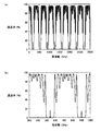
- (A) is the transmittance
- FIG. (B) is an enlarged view of the range of 300 to 1000 GHz of the transmittance spectrum of (a). It is a distribution map of the electric field strength inside a periodic structure.
- (A) is the transmittance
- FIG. (B) is the figure which expanded the range of 0.5395-0.5410 THz of the transmittance
- (C) is a graph which shows the relationship between the mass of a dielectric material, and peak transmittance
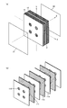
- (A) is a perspective view which shows the periodic structure used for the measurement of Example 2.
- FIG. (B) is an exploded perspective view of the first periodic structure portion 11 of (a). It is the transmittance
- FIG. (A) is the transmittance
- FIG. (B) is the graph which showed the relationship between the mass of a to-be-measured object, and peak transmittance
- (A) is the transmittance
- FIG. (B) is a graph showing the relationship between the peak frequency of the impurity mode (left scale: solid line) and the transmittance of the peak (right scale: dotted line) in the transmittance spectrum of (a) and the thickness of the gap portion. . It is a graph which shows the relationship between the material which comprises a periodic structure, the number of layers, and electric field strength in each condition of Example 4.
- (A) is a transmission spectrum near 180 GHz which is a fundamental mode
- (b) is a transmission spectrum near 540 GHz which is a third harmonic mode
- (c) is a transmission spectrum near 900 GHz which is a fifth harmonic mode. It is.
- (A) is the phase spectrum calculated
- (B) is an enlarged view in the vicinity of 180 GHz in (a)
- (c) is an enlarged view in the vicinity of 540 GHz in (a)
- (d) is an enlarged view in the vicinity of 900 GHz in (a).
- the present invention holds an object to be measured in a periodic structure, irradiates the periodic structure with an electromagnetic wave, detects an electromagnetic wave transmitted through the periodic structure, and disperses the electromagnetic wave dispersed in the periodic structure.
- the present invention relates to a measuring apparatus for measuring the characteristics of an object to be measured based on the fact that the frequency characteristic or phase characteristic of the object changes due to the presence of the object to be measured.
- the periodic structure includes a first periodic structure portion in which the complex dielectric constant periodically changes and a second periodic structure portion in which the complex dielectric constant periodically changes.
- the first periodic structure portion and the second periodic structure portion are disposed via a gap portion for disposing the object to be measured.
- the first periodic structure portion and the second periodic structure portion preferably have a structure in which flat plate-shaped high refractive index layers and flat plate-shaped low refractive index layers are alternately stacked.
- the high refractive index layer is a layer composed of a material having a higher refractive index than that of the low refractive index layer.
- the low refractive index layer is a layer composed of a material having a refractive index lower than that of the high refractive index layer.
- the gap portion is a gap portion between the first periodic structure portion and the second periodic structure portion.
- the first periodic structure portion and the second periodic structure portion are preferably arranged so that the main surface of the first periodic structure portion and the main surface of the second periodic structure portion are parallel to each other.
- the periodic structure may be arranged such that the main surfaces of the first periodic structure portion and the second periodic structure portion are perpendicular to the traveling direction of the electromagnetic wave applied to the first periodic structure portion. It may be arranged so as to be inclined.
- the material constituting the high refractive index layer is not particularly limited as long as it has a higher refractive index than that of the low refractive index layer, but a material having a low dielectric loss is preferable.
- a material having a low dielectric loss is preferable.
- quartz, calcium fluoride, ceramics, silicon, and the like can be given. Quartz is more preferable. This is because the electric field strength of the gap portion tends to become maximum as shown in Example 4 described later.
- the low refractive index layer and the gap portion are preferably spaces filled with gas.
- the gas is preferably a gas with little dielectric loss or a gas not containing water vapor, and examples thereof include dry nitrogen.
- the low refractive index layer may have a configuration in which a frame for forming the space is provided.
- the method for arranging the object to be measured in the gap part is not particularly limited, and examples thereof include a method for arranging a film holding the object to be measured in the gap part, a method for flowing a fluid containing the object to be measured through the gap part, and the like. It is done.
- the film for holding the object to be measured is not particularly limited, but a film having high transmittance of electromagnetic waves used for measurement is preferable. Therefore, the material of the film is preferably a material having a low dielectric constant (low dielectric loss), and examples thereof include polyethylene resin and polyamide resin.
- the thing with a thin film thickness is preferable, it is preferable to have the shape property for arrange
- the periodic structure is configured such that the main surfaces of the first periodic structure portion and the second periodic structure portion are perpendicular to the traveling direction of the electromagnetic wave irradiated to the first periodic structure portion. It is preferable to arrange
- measuring the property of the object to be measured is to perform various qualitative properties such as quantification of the compound to be measured and dielectric constant, for example, the content of a minute amount of the object to be measured such as in a solution. Or measuring the object to be measured.
- the electromagnetic wave used in the measurement method of the present invention is not particularly limited as long as the electromagnetic wave can cause scattering according to the structure of the plate-shaped periodic structure. Radio waves, infrared rays, visible rays, ultraviolet rays, X-rays Any of gamma rays and the like can be used.
- the frequency is not particularly limited, but is preferably 20 GHz to 120 THz, more preferably 100 GHz to 5 THz, and further preferably 100 GHz to 3 THz. Since the spatial resolution can be reduced when the frequency is 100 GHz or higher, high-sensitivity measurement is possible. When the frequency is higher than 5 THz, the thickness of the high refractive index layer needs to be thinner than about 15 ⁇ m. This is because it becomes difficult to process the high refractive index layer.
- the electromagnetic wave used in the present invention is usually an electromagnetic wave of 20 GHz to 120 THz.
- Specific electromagnetic waves include, for example, a terahertz wave generated by the optical rectification effect of an electro-optic crystal such as ZnTe using a short light pulse laser as a light source, an infrared ray emitted from a high-pressure mercury lamp or a ceramic lamp, or a semiconductor laser. Examples include visible light emitted and electromagnetic waves radiated from a photoconductive antenna.
- scattering means a broad concept including transmission, which is a form of forward scattering, and reflection, which is a form of backscattering, and is preferably transmission or reflection. More preferably, transmission in the 0th order direction or reflection in the 0th order direction.
- the grating interval of the diffraction grating is s
- the incident angle is i
- the diffraction angle is ⁇
- the wavelength is ⁇
- the measurement apparatus of the present invention includes an irradiation unit that irradiates the first periodic structure unit with an electromagnetic wave, a detection unit that detects the electromagnetic wave transmitted through the periodic structure and emitted from the second periodic structure unit, and It has.
- a waveguide is not used by interposing a gap portion between two periodic structure portions (one-dimensional, two-dimensional and three-dimensional photonic crystal regions) as described above.
- an impurity mode in the frequency characteristic or phase characteristic of the electromagnetic wave dispersed by the periodic structure can be generated.
- the impurity mode is a frequency characteristic or a phase characteristic that is generated when a gap part exists as a non-periodic part between two periodic structure parts, and is not found only in the periodic structure part. Or it is a phase characteristic. Further, by arranging the object to be measured in the gap portion and measuring the transmittance spectrum of the periodic structure, the characteristics of the object to be measured can be measured from the change of the impurity mode appearing in the transmittance spectrum.
- the periodic structure has a gap adjusting mechanism for changing the thickness of the gap portion.
- An impurity mode can be generated at an arbitrary frequency by the gap adjusting mechanism.
- the frequency characteristic of the device under test can be obtained in a wide frequency range.
- the phase characteristics of the device under test can be obtained in a wide frequency range.
- the electric field strength of the gap can be maximized by changing the width of the gap by the gap adjusting mechanism.
- one of the periodic structure portions may be fixed and the other periodic structure portion may be moved to change the width of the gap portion. Further, the width of the gap portion may be changed by simultaneously moving the two periodic structure portions.
- a distance adjusting mechanism for moving the object to be measured arranged in the gap part in a direction parallel to the traveling direction of the electromagnetic wave irradiated from the irradiation part.
- the distance between the first periodic structure body and the second periodic structure body and the object to be measured can be adjusted, and the same effect as the gap adjustment mechanism can be achieved.
- the device under test only needs to be disposed in the gap portion, and is desirably disposed in the center of the gap portion.
- a position adjusting mechanism for moving the object to be measured arranged in the gap part in a direction perpendicular to the traveling direction of the electromagnetic wave irradiated from the irradiation part.
- the film holding the object to be measured is moved in the gap portion, and the measurement object is measured at a plurality of locations in the plane of the film, whereby the retention rate of the object to be measured on the film is measured.
- In-plane variation can be averaged.
- a plurality of objects to be measured can be measured by a series of operations by holding different objects to be measured at a plurality of locations in the plane of one film.
- the gap adjusting mechanism, the distance adjusting mechanism, and the position adjusting mechanism have a guide in order to reduce parallelism.
- Examples of the gap adjusting mechanism, the distance adjusting mechanism, and the position adjusting mechanism include an automatic stage that is operated by a motor or an actuator, or a manual stage that is operated by a micrometer.
- FIG. 5 shows a conceptual diagram of a periodic structure, a gap adjusting mechanism, a distance adjusting mechanism, and a position adjusting mechanism in one embodiment of the present invention.
- the periodic structure shown in FIG. 5 includes a first periodic structure portion 11 and a second periodic structure portion 12, and the first periodic structure portion 11 and the second periodic structure portion 12 are 1 by a gap adjusting mechanism 51, 52. It can be arbitrarily moved in the axial direction (Z-axis direction), whereby the thickness of the gap portion can be adjusted.
- the film 4 holding the object to be measured can be arbitrarily moved in the X-axis and Y-axis directions by the position adjusting mechanisms 41 and 43, and can be arbitrarily moved in the Z-axis direction by the distance adjusting mechanism 42. Therefore, it can be arbitrarily moved in the triaxial direction within the gap portion.
- the low refractive index layer is a space surrounded by a frame, and the periodic structure has a structure for filling the space with gas from the outside.
- each of the high refractive index layers 11a is between the space portions 111 of the plurality of low refractive index layers 11b, and A structure provided with a through hole 110 for communicating the space 111 of the low refractive index layer 11b with the outside of the first periodic structure unit 11 may be mentioned.
- the noise peak when a dielectric such as water vapor exists in the space 111 of the low refractive index layer 11b is reduced. And the S / N ratio can be improved.
- the present invention holds an object to be measured in a periodic structure, irradiates the periodic structure with electromagnetic waves, detects electromagnetic waves transmitted through the periodic structures, and transmits electromagnetic waves through the periodic structures.
- the present invention also relates to a measurement method including a step of irradiating the first periodic structure part with an electromagnetic wave and a step of detecting an electromagnetic wave transmitted through the periodic structure and emitted from the second periodic structure part. .
- the measurement method used in the present invention is preferably a method using time domain terahertz spectroscopy (THz-TDS), but is not limited to such a method, and a measurement method using another spectroscopic device is also used.
- THz-TDS is a method in which a terahertz pulse wave is incident on a sample, the waveform of the terahertz pulse wave after being transmitted or reflected by the sample is time-resolved, and the waveform is Fourier transformed to obtain the amplitude and phase for each frequency. This is the spectroscopic method.
- information on the intensity of light is measured, but in terahertz pulse spectroscopy, the waveform of the electromagnetic wave itself is measured.
- the frequency dependence of the complex dielectric constant and complex refractive index of the sample can be examined.
- the physical and chemical properties of the sample can be explored by analyzing the frequency dependence of the complex dielectric constant.
- Example 1 A simulation calculation by electromagnetic field analysis was performed on the transmittance spectrum of the periodic structure. An outline of the model configuration of the measurement apparatus used for the calculation will be described with reference to FIG. FIG. 1B shows an enlarged view of a part of FIG. 1A (a part surrounded by a dotted line A).
- the periodic structure 1 includes a first port 31 (which serves as an irradiation unit and a detection unit), a second port 32 (a detection unit), and two periodic structure units (a first cycle). It is comprised from the structure part 11, the 2nd periodic structure part 12), and the gap part 2 between them.
- the first periodic structure portion 11 is composed of a total of seven layers, in which high refractive index layers 11a and low refractive index layers 11b are alternately stacked, and which includes four high refractive index layers 11a and three low refractive index layers 11b. It is configured. Similarly, in the second periodic structure portion 12, a high refractive index layer 12a and a low refractive index layer 12b are laminated.
- Fig. 3 shows a distribution diagram of the electric field strength inside the periodic structure obtained by the same simulation. A gradation is provided between white and black depending on the electric field strength. As shown in FIG. 3, when the electric field strengths of the two periodic structure parts (the first periodic structure part 11 and the second periodic structure part 12) and the gap part 2 are compared, a strong electric field is generated in the gap part 2. I understand.
- FIG. 4A shows the obtained transmittance spectrum (with a dielectric) and the above-described transmittance spectrum (without a dielectric) together. Moreover, what expanded the transmittance
- the transmittance at the peak of the impurity mode was 61% when there was no dielectric and 60% when there was a dielectric. From this result, it is understood that the transmittance of the peak of the impurity mode is lowered by disposing the dielectric in the gap portion.
- the obtained transmittance spectrum (with a dielectric) and the above-described transmittance spectrum (without a dielectric) are shown together in FIG. 11A shows a transmittance spectrum near 180 GHz, which is the fundamental mode (lowest order frequency), FIG. 11B shows a transmittance spectrum around 540 GHz, which is the third harmonic mode, and FIG. 11C. Is a transmittance spectrum near 900 GHz which is a fifth harmonic mode. It can be seen that the attenuation of the transmittance of the impurity mode caused by the dielectric increases as the higher mode is reached.
- the transmittance at the peak of the impurity mode is 91.5% to 79.2% in the fundamental mode, 77.3% to 36.2% in the third harmonic, and 66. It has changed from 2% to 18.0%.
- the obtained transmittance spectrum (with a dielectric) and the above-described transmittance spectrum (without a dielectric) are shown together in FIG. 12A shows a transmittance spectrum in the vicinity of 180 GHz, which is the fundamental mode (lowest order frequency)
- FIG. 12B shows a transmittance spectrum in the vicinity of 540 GHz, which is the third harmonic mode
- the frequency of the impurity mode is shifted to the low frequency side by the dielectric. Further, it can be seen that the frequency shift amount of the impurity mode increases as the higher order mode is reached.
- the frequency shift amount of the impurity mode due to the dielectric is 0.5 GHz for the fundamental mode, 1.5 GHz for the third harmonic, and 2 GHz for the fifth harmonic.
- FIG. 13A shows the obtained phase spectrum (with a dielectric) and the phase spectrum when there is no dielectric.
- 13A is an enlarged view in the vicinity of 180 GHz that is the basic mode
- FIG. 13B is an enlarged view in the vicinity of 540 GHz that is the third harmonic mode.
- An enlarged view of the vicinity of 900 GHz which is a wave mode is shown in FIG. Due to the presence of the dielectric on the flat plate in the gap, the phase changes at a frequency near the impurity mode. Moreover, it turns out that the phase change produced by a dielectric material becomes large as it becomes a higher order mode.
- the phase at the frequency of the impurity mode is changed by 0.96 rad (180 GHz) for the fundamental mode and 1.29 rad (540 GHz) for the third harmonic wave and 1.36 rad (900 GHz) for the fifth harmonic wave depending on the dielectric. Yes.
- an impurity mode can be generated without using a waveguide.
- the change in the peak of the impurity mode appearing in the transmittance spectrum and the change in the phase spectrum can be used. It can be seen that the characteristics can be measured.
- Example 2 Measurement was performed on the transmittance spectrum of the periodic structure shown in FIGS.
- the periodic structure 1 shown in FIGS. 6A and 6B includes an input / output port (first port 31 and second port 32) and two periodic structure parts (first periodic structure part 11 and second period).
- the first periodic structure portion 11 is composed of a total of seven layers, in which high refractive index layers 11a and low refractive index layers 11b are alternately stacked, and which includes four high refractive index layers 11a and three low refractive index layers 11b. It is constructed and fixed by thermocompression bonding. Similarly, in the second periodic structure portion 12, a high refractive index layer 12a and a low refractive index layer 12b are laminated.
- FIG. 6B is an exploded perspective view of the first periodic structure portion 11 in FIG.
- the high refractive index layer 11a is provided with four through holes 110 having a diameter of 4 mm.
- the low refractive index layers 11b and 12b are configured by a frame plate made of quartz having a thickness of 417 ⁇ m, and a square space portion 111 having a side of 14 mm is provided at the center.
- the space 111 is filled with dry nitrogen through the through hole 110. This is because the terahertz electromagnetic wave is very absorbed by water vapor in the air.
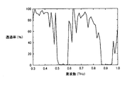
- FIG. 7 shows the transmittance spectrum obtained by performing Fourier transform on the terahertz pulse wave obtained in the above. As shown in FIG. 7, it can be seen that a photonic band gap appears in the frequency band from 0.5 THz to 0.6 THz, and a peak (near 0.54 THz) due to the impurity mode occurs in the photonic band gap.
- the preparation procedure of the sample will be described.
- Five glucose aqueous solutions (0 ng / ⁇ L, 10 ng / ⁇ L, 30 ng / ⁇ L, 50 ng / ⁇ L, 1000 ng / ⁇ L) were prepared, and 20 ⁇ L was uniformly dropped onto each of the five membrane filters (drop area 398 mm 2 ). did.
- the membrane filter was dried at room temperature in a drying container for 24 hours to precipitate glucose.
- As the porous film a polyethylene film having a plurality of holes having a diameter of 5 ⁇ m, an overall shape of a disk having a diameter of 47 mm, and a thickness of 100 ⁇ m was used.
- Each membrane filter was placed one by one in the center in the thickness direction of the gap portion of the periodic structure shown in FIG. 6, and the transmittance spectrum was measured. At that time, the membrane filter was moved in a plane perpendicular to the traveling direction of the electromagnetic wave, and the average of the transmittance spectra at three different points in the plane of the membrane filter was obtained. The transmittance spectrum obtained by the measurement is shown in FIG.
- FIG. 8 (a) shows the respective transmittance spectra corresponding to (a) to (e).
- FIG. 8A shows that the transmittance of the impurity mode generated at 549 GHz changes depending on the amount of glucose.
- FIG. 8B is a graph showing the relationship between the transmittance at 549 GHz and the mass of the object to be measured. 75.6 ng, 126 ng, and 2500 ng of glucose can be distinguished significantly.
- Example 3 A simulation calculation by electromagnetic field analysis was performed for the transmittance spectrum when the thickness of the gap portion in the periodic structure was changed.
- the thickness of the gap portion 12 was systematically changed from 0 ⁇ m to 556 ⁇ m to the seven-stage thickness shown in FIG. 9A. Except for the above, simulation calculation was performed in the same manner as in Example 1.
- the transmittance spectrum with respect to the thickness of the gap portion 12 is shown in FIG. FIG. 9B plots the thickness of the gap portion 12 on the horizontal axis and the frequency or transmittance of the impurity mode on the vertical axis.
- FIGS. 9A and 9B show that both the frequency and the transmittance of the impurity mode change systematically according to the thickness of the gap portion 12. That is, as shown in FIGS. 9A and 9B, as the gap portion increases from 0 ⁇ m to 556 ⁇ m, the size of the transmittance peak in the impurity mode increases. Further, as the gap portion increases from 0 ⁇ m to 556 ⁇ m, the peak frequency of the impurity mode transmittance decreases. Numerical data of FIGS. 9A and 9B are shown in Table 1.
- the impurity mode can be generated at an arbitrary frequency by controlling the thickness of the gap portion in the periodic structure (the positional relationship between the two periodic structure portions). As a result, it is considered that the frequency characteristics of the device under test can be obtained in a wide frequency range.
- Example 4 A simulation calculation was performed by electromagnetic field analysis on the relationship between the number or material of the high refractive index layers and the low refractive index layers constituting the two periodic structure portions and the electric field strength of the gap portion at the frequency of the impurity mode.
- the high refractive index layers 11a and 12a are the following three types (a) to (c).
- the total number of layers of the high refractive index layer and the low refractive index layer was changed.
- simulation calculation was performed using a periodic structure similar to the periodic structure shown in FIG. 1 as a model in the simulation of Example 1.
- the end faces in the X-axis direction and the Y-axis direction are periodic boundaries, and the end faces in the Z-axis direction are absorption boundaries.
- An electromagnetic wave is input from the first port, and the electromagnetic wave reflected by the periodic structure is detected by the first port 31, and the electromagnetic wave transmitted through the periodic structure is detected by the second port 32.
- the electric field strength at the center in the thickness direction of the gap 2 at the impurity mode frequency (549 GHz) was obtained.
- the relationship between the number of layers and the electric field strength under each condition is shown in FIG. The number of layers in FIG.
- the number of layers of the second periodic structure unit 12 is the number of layers in the first periodic structure unit 11. It is the same as the number of layers.
- the characteristics of the object to be measured are measured based on the fact that the frequency or transmittance of the impurity mode in the frequency characteristics varies depending on the existence of the object to be measured.
- the characteristic of the object to be measured may be measured based on the change due to the above.
- SYMBOLS 1 Periodic structure 11 1st periodic structure part, 11a High refractive index layer, 11b Low refractive index layer, 110 Through-hole, 111 Space part, 12 2nd periodic structure part, 12a High refractive index layer, 12b Low refractive index Layer, 2 gap part, 31 1st port, 32 2nd port, 4 film, 41, 43 Position adjustment mechanism, 42 Distance adjustment mechanism, 51, 52 Gap adjustment mechanism.
Landscapes
- Physics & Mathematics (AREA)
- Spectroscopy & Molecular Physics (AREA)
- Health & Medical Sciences (AREA)
- Analytical Chemistry (AREA)
- Life Sciences & Earth Sciences (AREA)
- Chemical & Material Sciences (AREA)
- Toxicology (AREA)
- Biochemistry (AREA)
- General Health & Medical Sciences (AREA)
- General Physics & Mathematics (AREA)
- Immunology (AREA)
- Pathology (AREA)
- Investigating Or Analysing Materials By Optical Means (AREA)
Abstract
本発明は、周期的構造体に被測定物を保持し、前記周期的構造体(1)に電磁波を照射して、前記周期的構造体(1)を透過した電磁波を検出し、前記周期的構造体(1)で分散した電磁波の周波数特性もしくは位相特性が前記被測定物の存在により変化することに基づいて被測定物の特性を測定するための測定装置であって、前記周期的構造体(1)は、前記被測定物を配置するためのギャップ部(2)を介して配置された複素誘電率が周期的に変化する第1周期構造部(11)および第2周期構造部(12)からなることを特徴とする。
Description
本発明は、物質の特性を分析するのに、平板形状の周期的構造体に被測定物を保持して、その被測定物が保持された平板形状の周期的構造体に電磁波を照射し、散乱された電磁波を検出して被測定物の特性を測定するための測定装置、および測定方法に関する。
従来から、物質の特性を分析するのに、特定の構造体に被測定物を保持して、その被測定物が保持された構造体に電磁波を照射し、その透過スペクトルを解析して被測定物の特性を検出する測定方法が用いられている。具体的には、例えば、金属メッシュフィルタに付着したタンパク質などの被測定物に、テラヘルツ波を照射して透過スペクトルを解析する手法が挙げられる。
このような電磁波を用いた透過スペクトルの解析手法の従来技術として、特開2008-185552号公報(特許文献1)には、被測定物が保持された空隙領域を有する空隙配置構造体(具体的には、メッシュ状の導体板)に向かって、空隙配置構造体の主面に垂直な方向に対して斜めの方向から電磁波を照射して、空隙配置構造体を透過した電磁波を測定し、測定値の周波数特性に生じたディップ波形の位置が、被測定物の存在により移動することに基づいて被測定物の特性を検出する測定方法が開示されている。
一方、別の形態の構造体を用いた測定装置の例として、特開2006-234692号公報(特許文献2)には、被測定物を流す為の流路が形成された2つのフォトニック結晶領域を有形の光導波路によって接続した測定装置が開示されている。フォトニック結晶とは、屈折率が周期的に変化する構造体であり、その中の電磁波の伝わり方は構造によって制御できる。各々のフォトニック結晶領域にはさらに欠陥構造が形成されている。
このような構造の複合構造体に特定の電磁波を照射した場合、その透過率スペクトルには欠陥構造に起因する不純物モードが現れる。フォトニック結晶の流路内に被測定物を流し、複合構造体の透過率スペクトル中の不純物モードの変化を測定することで、流路内にある被測定物の特性を測定することができる。この方法では、欠陥準位によって透過率スペクトルに生じる不純物モードのピークの位置ずれに基づいて測定が行われる(特許文献2の[0033]、[0045]~[0054]、図5および6参照)。
しかし、特許文献2に開示された測定装置においては、2つのフォトニック結晶領域を接続する導波路が必要である。導波路が固定されてしまうと、光路長が固定されるので自ずと不純物モードが固定されてしまう。また、導波路によって使用できる周波数帯が制限されるので、不純物モードの周波数も固定されてしまう。このため、被測定物の種類などに応じて、最適な不純物モードが出現するように、電磁波の周波数や装置構成を調節することが困難になるという問題があった。
本発明は、フォトニック結晶のような周期構造部を有する装置を用いて被測定物の測定を行う場合において、被測定物の種類などに応じて、最適な不純物モードが出現するように、電磁波の周波数や装置構成を調節することが可能な測定装置を提供し、被測定物の測定を高感度に再現性良く行うことを目的とする。
本発明は、周期的構造体に被測定物を保持し、上記周期的構造体に電磁波を照射して、上記周期的構造体を透過した電磁波を検出し、上記周期的構造体で分散した電磁波の周波数特性もしくは位相特性が上記被測定物の存在により変化することに基づいて被測定物の特性を測定するための測定装置であって、
上記周期的構造体は、上記被測定物を配置するためのギャップ部を介して配置された複素誘電率が周期的に変化する第1周期構造部および第2周期構造部からなり、
上記第1周期構造部へ電磁波を照射する照射部と、上記周期的構造体を透過して上記第2周期構造部から出射される電磁波を検出する検出部とを備えた測定装置である。
上記周期的構造体は、上記被測定物を配置するためのギャップ部を介して配置された複素誘電率が周期的に変化する第1周期構造部および第2周期構造部からなり、
上記第1周期構造部へ電磁波を照射する照射部と、上記周期的構造体を透過して上記第2周期構造部から出射される電磁波を検出する検出部とを備えた測定装置である。
上記周期的構造体は、平板形状の高屈折率層と平板形状の低屈折率層とが交互に積層された構造を有することが好ましい。
上記周波数特性もしくは位相特性における不純物モードの周波数、透過率または位相が上記被測定物の存在により変化することに基づいて被測定物の特性を測定することが好ましい。
上記周波数特性もしくは位相特性における不純物モードのうち、最低次の周波数の整数倍の周波数における不純物モードの周波数、透過率または位相が、上記被測定物の存在により変化することに基づいて被測定物の特性を測定することが好ましい。
上記周期的構造体において、上記ギャップ部の厚さを変化させるためのギャップ調節機構を有することが好ましい。
上記ギャップ部に配置された上記被測定物を、ギャップ内で任意に移動する為の位置調節機構を有することが好ましい。
上記低屈折率層が枠体に囲まれた空間であり、
上記周期的構造体が、該空間に外部から気体を充填するための構造を有することが好ましい。
上記周期的構造体が、該空間に外部から気体を充填するための構造を有することが好ましい。
また、本発明は、周期的構造体に被測定物を保持し、上記周期的構造体に電磁波を照射して、上記周期的構造体を透過した電磁波を検出し、上記周期的構造体を透過した電磁波の周波数特性もしくは位相特性が上記被測定物の存在により変化することに基づいて被測定物の特性を測定する測定方法であって、
上記周期的構造体は、上記被測定物を配置するためのギャップ部を介して配置された複素誘電率が周期的に変化する第1周期構造部および第2周期構造部からなり、
上記第1周期構造部へ電磁波を照射する工程と、上記周期的構造体を透過して上記第2周期構造部から出射される電磁波を検出する工程とを含む、測定方法にも関する。
上記周期的構造体は、上記被測定物を配置するためのギャップ部を介して配置された複素誘電率が周期的に変化する第1周期構造部および第2周期構造部からなり、
上記第1周期構造部へ電磁波を照射する工程と、上記周期的構造体を透過して上記第2周期構造部から出射される電磁波を検出する工程とを含む、測定方法にも関する。
本発明の測定装置および測定方法によれば、フォトニック結晶のような周期構造部を有する装置を用いて被測定物の測定を行う場合において、導波路を用いなくても不純物モードを生じさせることができる。このため、ギャップ部の厚さ(光路長)を調節することができ、任意の周波数に不純物モードを生じさせることができる。
また、ギャップ部の電界強度がより強くなるように、不純物モードが出現する周波数が調節された周期的構造体に、適切な周波数の電磁波を照射して不純物モードを発生させることにより、被測定物をギャップ部に配置したときの不純物モードの変化量を大きくすることができる。これにより、不純物モードの変化に基づいた被測定物の測定を、高感度に再現性良く行うことができる。
(測定装置)
本発明は、周期的構造体に被測定物を保持し、上記周期的構造体に電磁波を照射して、上記周期的構造体を透過した電磁波を検出し、上記周期的構造体で分散した電磁波の周波数特性もしくは位相特性が上記被測定物の存在により変化することに基づいて被測定物の特性を測定するための測定装置に関するものである。
本発明は、周期的構造体に被測定物を保持し、上記周期的構造体に電磁波を照射して、上記周期的構造体を透過した電磁波を検出し、上記周期的構造体で分散した電磁波の周波数特性もしくは位相特性が上記被測定物の存在により変化することに基づいて被測定物の特性を測定するための測定装置に関するものである。
上記周期的構造体は、複素誘電率が周期的に変化する第1周期構造部、および、複素誘電率が周期的に変化する第2周期構造部からなる。第1周期構造部および第2周期構造部は、被測定物を配置するためのギャップ部を介して配置される。第1周期構造部および第2周期構造部は、平板形状の高屈折率層と平板形状の低屈折率層とが交互に積層された構造を有することが好ましい。高屈折率層とは、低屈折率層よりも屈折率の高い材料から構成される層である。低屈折率層とは、高屈折率層よりも屈折率の低い材料から構成される層である。ギャップ部とは第1周期構造部と第2周期構造部との間隙部分である。第1周期構造部および第2周期構造部は、第1周期構造部の主面と第2周期構造部の主面とが平行となるように配置されることが好ましい。上記周期的構造体は、例えば、第1周期構造部および第2周期構造部の主面が、第1周期構造部へ照射される電磁波の進行方向に対して垂直となるように配置されてもよく、斜めになるように配置されてもよい。
高屈折率層を構成する材料は、低屈折率層よりも高い屈折率を有する材料であれば特に限定されないが、誘電損失の少ない材料が好ましい。例えば、照射部から照射される電磁波の周波数が100GHz~3THzである場合、石英、フッ化カルシウム、セラミックス、シリコンなどが挙げられる。さらに好ましくは石英である。後述の実施例4に示されるように、ギャップ部の電界強度が最大になる傾向があるためである。
低屈折率層およびギャップ部は、気体を充填した空間であることが好ましい。ここで、該気体は、誘電損失の少ない気体や水蒸気を含まない気体などであることが好ましく、例えば、乾燥窒素などが挙げられる。なお、低屈折率層は、該空間を形成するための枠体が設けられた構成となっていてもよい。
ギャップ部に被測定物を配置する方法は特に限定されないが、例えば、被測定物が保持されたフィルムをギャップ部に配置する方法や、被測定物を含む流体をギャップ部に流す方法などが挙げられる。被測定物を保持するフィルムは特に限定されないが、測定に用いる電磁波の透過率が高いものが好ましい。したがって、フィルムの材質としては、誘電率の小さな(誘電損失の少ない)材料であることが好ましく、例えば、ポリエチレン樹脂、ポリアミド樹脂などが挙げられる。また、フィルムの厚さは薄いものが好ましいが、ギャップ部に配置するための定形性を有することが好ましい。また、被測定物を効率的に保持するために多孔を有するものであることが好ましい。
本発明の測定装置において、上記周期的構造体は、第1周期構造部および第2周期構造部の主面が、第1周期構造部へ照射される電磁波の進行方向に対して垂直となるように配置されることが好ましい。
本発明において、被測定物の特性を測定するとは、被測定物となる化合物の定量や誘電率等の各種の定性などを行うことであり、例えば、溶液中等の微量の被測定物の含有量を測定する場合や、被測定物の同定を行う場合が挙げられる。
本発明の測定方法で用いられる電磁波は、平板形状の周期的構造体の構造に応じて散乱を生じさせることのできる電磁波であれば特に限定されず、電波、赤外線、可視光線、紫外線、X線、ガンマ線等のいずれも使用することができる。また、その周波数も特に限定されるものではないが、好ましくは20GHz~120THzであり、より好ましくは100GHz~5THzであり、さらに好ましくは100GHz~3THzである。100GHz以上の周波数とする方が、空間分解能を小さくできるので高感度の測定が可能になり、5THzより高い周波数とした場合、高屈折率層の厚さを15μm程度よりも薄くする必要があるため高屈折率層の加工が困難になるためである。
また、本発明で用いられる電磁波は、通常、20GHz~120THzの電磁波である。具体的な電磁波としては、例えば、短光パルスレーザを光源として、ZnTe等の電気光学結晶の光整流効果により発生するテラヘルツ波や、高圧水銀ランプやセラミックランプから放射される赤外線や、半導体レーザーから出射される可視光や光伝導アンテナから放射される電磁波が挙げられる。
本発明において「散乱」とは、前方散乱の一形態である透過や、後方散乱の一形態である反射などを含む広義の概念を意味し、好ましくは透過や反射である。さらに好ましくは、0次方向の透過や0次方向の反射である。
なお、一般的に、回折格子の格子間隔をs、入射角をi、回折角をθ、波長をλとしたとき、回折格子によって回折されたスペクトルは、
s(sin i -sin θ)=nλ …(1)
と表すことができる。上記「0次方向」の0次とは、上記式(1)のnが0の場合を指す。sおよびλは0となり得ないため、n=0が成立するのは、sin i- sin θ=0の場合のみである。従って、上記「0次方向」とは、入射角と回折角が等しいとき、つまり電磁波の進行方向が変わらないような方向を意味する。
s(sin i -sin θ)=nλ …(1)
と表すことができる。上記「0次方向」の0次とは、上記式(1)のnが0の場合を指す。sおよびλは0となり得ないため、n=0が成立するのは、sin i- sin θ=0の場合のみである。従って、上記「0次方向」とは、入射角と回折角が等しいとき、つまり電磁波の進行方向が変わらないような方向を意味する。
なお、本発明の測定装置は、上記第1周期構造部へ電磁波を照射する照射部と、上記周期的構造体を透過して上記第2周期構造部から出射される電磁波を検出する検出部とを備えている。
本発明の測定装置においては、上記のように2つの周期構造部(1次元、2次元および3次元構造のフォトニック結晶領域)の間にギャップ部を介在させることにより、導波路を用いなくても、周期的構造体で分散された電磁波の周波数特性もしくは位相特性における不純物モードを生じさせることができる。
上記周波数特性もしくは位相特性における不純物モードの周波数、透過率または位相が、上記被測定物の存在により変化することに基づいて被測定物の特性を測定することが好ましい。本発明において、不純物モードとは、2つの周期構造部の間に非周期的な部分としてギャップ部が存在することにより生じる周波数特性もしくは位相特性であり、周期構造部のみには見られない周波数特性もしくは位相特性である。また、被測定物をギャップ部に配置し、周期的構造体の透過率スペクトルを測定することで、透過率スペクトルに出現する不純物モードの変化から被測定物の特性を測定できる。
上記周期的構造体において、上記ギャップ部の厚さを変化させるためのギャップ調節機構を有することが好ましい。ギャップ調節機構により、任意の周波数に不純物モードを生じさせられる。その結果、被測定物の周波数特性を広い周波数範囲で得ることができる。また、被測定物の位相特性を広い周波数範囲で得ることができる。
また、ギャップ調節機構によりギャップ部の幅を変えることで、ギャップ部の電界強度を最大にすることができる。ギャップ部の幅を変える場合、周期構造部の一方を固定し、他方の周期構造部を移動させてギャップ部の幅を変えてもよい。また、2つの周期構造部を同時に移動させてギャップ部の幅を変えてもよい。
上記ギャップ部に配置された上記被測定物を、上記照射部から照射される電磁波の進行方向に対して平行な方向に移動するための距離調節機構を有することが好ましい。このような距離調節機構によって、第1周期構造体および第2周期構造体と被測定物との距離を調節することができ、ギャップ調節機構と同様の効果が奏される。また、被測定物はギャップ部に配置されていればよく、望ましくはギャップ部の中央に配置される。
上記ギャップ部に配置された上記被測定物を、上記照射部から照射される電磁波の進行方向に対して垂直な方向に移動するための位置調節機構を有することが好ましい。このような位置調節機構により、ギャップ部において、被測定物が保持されたフィルムを移動させ、フィルムの面内の複数箇所の被測定物を測定することで、被測定物のフィルムへの保持率の面内ばらつきを平均化することができる。また、1つのフィルムの面内の複数箇所に異なる被測定物を保持しておくことで、複数の被測定物を一連の操作で測定することもできる。
上記ギャップ調節機構と距離調節機構と位置調節機構は互いの平行度を小さくする為、ガイドを有していることが好ましい。また、上記ギャップ調節機構、距離調節機構および位置調節機構として、モーターやアクチュエーターで稼働する自動ステージ、もしくはマイクロメーターで稼働する手動ステージなどが挙げられる。
図5に、本発明の一形態における周期的構造体とギャップ調節機構、距離調節機構および位置調節機構の概念図を示す。図5に示す周期的構造体は第1周期構造部11および第2周期構造部12から構成されており、第1周期構造部11および第2周期構造部12はギャップ調節機構51,52により1軸方向(Z軸方向)に任意に移動させることができ、これによってギャップ部の厚さを調節することができる。また、被測定物が保持されたフィルム4は、位置調節機構41および43によりX軸およびY軸方向に任意に移動させることができ、距離調節機構42によりZ軸方向に任意に移動させることができるため、ギャップ部内において3軸方向に任意に移動させることができる。
上記低屈折率層が枠体に囲まれた空間であり、上記周期的構造体が、該空間に外部から気体を充填するための構造を有することが好ましい。例えば、図6(a)、(b)に示すように、第1周期構造部11において、高屈折率層11aの各々が、複数の低屈折率層11bの空間部111同士の間、および、低屈折率層11bの空間部111と第1周期構造部11の外部とを連通させるための貫通孔110を備えた構造が挙げられる。貫通孔110から乾燥窒素などを低屈折率層11bの空間部111に充填することにより、低屈折率層11bの空間部111内に水蒸気などの誘電体が存在した場合のノイズピークを低減することができ、S/N比を向上させることができる。
(測定方法)
本発明は、周期的構造体に被測定物を保持し、上記周期的構造体に電磁波を照射して、上記周期的構造体を透過した電磁波を検出し、上記周期的構造体を透過した電磁波の周波数特性もしくは位相特性が上記被測定物の存在により変化することに基づいて被測定物の特性を測定する測定方法であって、
上記周期的構造体は、複素誘電率が周期的に変化する第1周期構造部および第2周期構造部が、被測定物を配置するためのギャップ部を介して配置されており、
上記第1周期構造部へ電磁波を照射する工程と、上記周期的構造体を透過して上記第2周期構造部から出射される電磁波を検出する工程とを含む、測定方法にも関するものである。
本発明は、周期的構造体に被測定物を保持し、上記周期的構造体に電磁波を照射して、上記周期的構造体を透過した電磁波を検出し、上記周期的構造体を透過した電磁波の周波数特性もしくは位相特性が上記被測定物の存在により変化することに基づいて被測定物の特性を測定する測定方法であって、
上記周期的構造体は、複素誘電率が周期的に変化する第1周期構造部および第2周期構造部が、被測定物を配置するためのギャップ部を介して配置されており、
上記第1周期構造部へ電磁波を照射する工程と、上記周期的構造体を透過して上記第2周期構造部から出射される電磁波を検出する工程とを含む、測定方法にも関するものである。
本発明に用いられる測定方法は、時間領域テラヘルツ分光法(THz-TDS)を用いた方法であることが好ましいが、このような方法に限定されず、その他の分光装置を用いた測定方法も用いることができる。THz-TDSとは、テラヘルツパルス波をサンプルに入射させ、サンプルを透過もしくは反射した後のテラヘルツパルス波の波形を時間分解計測し、その波形をフーリエ変換することにより周波数ごとの振幅と位相を得るという分光法である。従来の分光装置において計測されるのは光の強度に関する情報であったが、テラヘルツパルス分光法では電磁波の波形そのものが計測される。テラヘルツパルス分光法を用いて得られた振幅と位相を解析することにより、サンプルの複素誘電率や複素屈折率の周波数依存性を調べることができる。さらに複素誘電率の周波数依存性の解析から、サンプルの物理的・化学的な性質を探ることができます。
以下、実施例を挙げて本発明をより詳細に説明するが、本発明はこれらに限定されるものではない。
(実施例1)
周期的構造体の透過率スペクトルについて、電磁界解析によるシミュレーション計算を行った。計算に用いた測定装置のモデル構成の概要について、図1(a)を用いて説明する。なお、図1(b)に、図1(a)の一部(Aの点線で囲まれた部分)を拡大した図を示す。
周期的構造体の透過率スペクトルについて、電磁界解析によるシミュレーション計算を行った。計算に用いた測定装置のモデル構成の概要について、図1(a)を用いて説明する。なお、図1(b)に、図1(a)の一部(Aの点線で囲まれた部分)を拡大した図を示す。
図1(a)に示されるように周期的構造体1は、第1ポート31(照射部と検出部を兼ねる)および第2ポート32(検出部)と、2つの周期構造部(第1周期構造部11、第2周期構造部12)およびその間のギャップ部2とから構成されている。
第1周期構造部11は、高屈折率層11aと低屈折率層11bとが交互に積層され、4層の高屈折率層11aと3層の低屈折率層11bとからなる計7層から構成されている。第2周期構造部12も同様に高屈折率層12aと低屈折率層12bとが積層されている。
シミュレーション計算において、高屈折率層11aおよび12aは、石英からなる層を想定して、比誘電率εr=3.8(屈折率1.95)、誘電損失tanδ=0.0004とし、厚さ213μmとした。低屈折率層11bおよび12bは、比誘電率εr=1、誘電損失tanδ=0とし、厚さ417μmとした。また、ギャップ部の比誘電率は、比誘電率εr=1、誘電損失tanδ=0とし、厚さ834μmとした。
(1) 周期的構造体のみの場合のシミュレーション
図1(a)に示すX軸方向、Y軸方向の端面を周期境界、Z軸方向の端面は吸収境界とした。第1ポート31からは電磁波が入力され、周期的構造体1で反射された電磁波が第1ポート31で検出され、周期的構造体1を透過した電磁波が第2ポート32で検出されるものとした。第1ポート31から入力した電磁波に対する第2ポート32で検出した電磁波の比を求め、透過率スペクトルを計算した。得られた透過率スペクトルを図2(a)に示す。また、図2(a)の300GHz~1000GHzの拡大図を図2(b)に示す。
図1(a)に示すX軸方向、Y軸方向の端面を周期境界、Z軸方向の端面は吸収境界とした。第1ポート31からは電磁波が入力され、周期的構造体1で反射された電磁波が第1ポート31で検出され、周期的構造体1を透過した電磁波が第2ポート32で検出されるものとした。第1ポート31から入力した電磁波に対する第2ポート32で検出した電磁波の比を求め、透過率スペクトルを計算した。得られた透過率スペクトルを図2(a)に示す。また、図2(a)の300GHz~1000GHzの拡大図を図2(b)に示す。
図2(a)、(b)の透過率スペクトルに示されるように、180GHz近傍でフォトニックバンドギャップおよび1次の不純物モードが現れ、約180GHzの奇数(n)倍の周波数(180GHz、540GHz、900GHz、・・・)でn次の不純物モードが生じることが分かる。高屈折率層を構成する厚さ213μmの石英は低屈折率層の厚さ415.35μm(=213×1.95)に相当する。この415μmと低屈折率部の厚さ417μmとを合わせた長さ(832μm)に電磁波の1波長がのる周波数[=光速(m/秒)/波長(μm)=360GHz]の電磁波が周期構造体を透過する。この長さに半波長がのる周波数180GHzの電磁波は周期構造体で反射されるため、約180GHzの奇数(n)倍の周波数で不純物モードが生じていると考えられる。
同様のシミュレーションによって得られる、周期構造体内部における電界強度の分布図を図3に示す。電界強度により白と黒の間で諧調を設けている。図3に示されるように2つの周期構造部(第1周期構造部11および第2周期構造部12)とギャップ部2の電界強度を比較すると、ギャップ部2において強い電界が生じていることが分かる。
(2) ギャップ部に誘電体が存在する場合のシミュレーション
次に、ギャップ部の厚さ方向中央に(第1周期構造部と第2周期構造部との距離が等間隔となるように)平板形状の誘電体が存在する場合の透過率スペクトルをシミュレーション計算した。計算には周期構造部の各層を縦続行列に変換し、各行列の積を散乱行列に変換する方法を用いた。また、計算における周波数分解能は400MHzである。
次に、ギャップ部の厚さ方向中央に(第1周期構造部と第2周期構造部との距離が等間隔となるように)平板形状の誘電体が存在する場合の透過率スペクトルをシミュレーション計算した。計算には周期構造部の各層を縦続行列に変換し、各行列の積を散乱行列に変換する方法を用いた。また、計算における周波数分解能は400MHzである。
平板形状の誘電体は、比誘電率εr=2.6、誘電損失tanδ=0.01とし、厚さ10nmとした。求めた透過率スペクトル(誘電体あり)と上述の透過率スペクトル(誘電体なし)を併せて図4(a)に示す。また、図4(a)の540GHz近傍の透過率スペクトルを拡大したものを図4(b)に示す。
不純物モードのピークにおける透過率は、誘電体がない状態が61%、誘電体がある状態が60%であった。この結果から、ギャップ部に誘電体を配置することで、不純物モードのピークの透過率が低下していることが分かる。
(3) ギャップ部の誘電体の厚さを変化させた場合のシミュレーション
さらに、誘電体の厚さを8段階(0(誘電体なし)、1nm~10μm)で変化させたときの、誘電体の質量と不純物モードの透過率の関係を求めた。誘電体の質量は、平板形状の誘電体の底面積を10mm2、誘電体の比重を1g/cm3として算出した。その結果を図4(c)に示す。図4(c)から、誘電体の質量が増えると、不純物モードの透過率が低下することが分かる。
さらに、誘電体の厚さを8段階(0(誘電体なし)、1nm~10μm)で変化させたときの、誘電体の質量と不純物モードの透過率の関係を求めた。誘電体の質量は、平板形状の誘電体の底面積を10mm2、誘電体の比重を1g/cm3として算出した。その結果を図4(c)に示す。図4(c)から、誘電体の質量が増えると、不純物モードの透過率が低下することが分かる。
(4) ギャップ部に誘電体が存在する状態での、不純物モードにおける高次モードと透過率との関連特性に関するシミュレーション
ギャップ部の厚さ方向中央に(第1周期構造部と第2周期構造部との距離が等間隔となるように)平板形状の誘電体が存在する場合の透過率スペクトルをシミュレーション計算した。計算には周期構造部の各層を縦続行列に変換し、各行列の積を散乱行列に変換する方法を用いた。また、計算における周波数分解能は1.25GHzである。
ギャップ部の厚さ方向中央に(第1周期構造部と第2周期構造部との距離が等間隔となるように)平板形状の誘電体が存在する場合の透過率スペクトルをシミュレーション計算した。計算には周期構造部の各層を縦続行列に変換し、各行列の積を散乱行列に変換する方法を用いた。また、計算における周波数分解能は1.25GHzである。
平板形状の誘電体は、比誘電率εr=2.6、誘電損失tanδ=0.01とし、厚さ1μmとした。求めた透過率スペクトル(誘電体あり)と上述の透過率スペクトル(誘電体なし)を併せて図11に示す。また、図11(a)は基本モード(最低次の周波数)である180GHz近傍の透過率スペクトル、図11(b)は3倍波のモードである540GHz近傍の透過率スペクトル、図11(c)は5倍波のモードである900GHz近傍の透過率スペクトルである。高次モードになるにつれて、誘電体によって生じる不純物モードの透過率の減衰が大きくなっていることが分かる。
なお、誘電体によって不純物モードのピークにおける透過率は、基本モードの場合91.5%から79.2%、3倍波の場合77.3%から36.2%、5倍波の場合66.2%から18.0%に変化している。
(5) ギャップ部に誘電体が存在する状態での、不純物モードにおける高次モードと周波数シフト量との関連特性に関するシミュレーション
ギャップ部の厚さ方向中央に(第1周期構造部と第2周期構造部との距離が等間隔となるように)平板形状の誘電体が存在する場合の透過率スペクトルをシミュレーション計算した。計算には周期構造部の各層を縦続行列に変換し、各行列の積を散乱行列に変換する方法を用いた。また、計算における周波数分解能は0.5GHzである。
ギャップ部の厚さ方向中央に(第1周期構造部と第2周期構造部との距離が等間隔となるように)平板形状の誘電体が存在する場合の透過率スペクトルをシミュレーション計算した。計算には周期構造部の各層を縦続行列に変換し、各行列の積を散乱行列に変換する方法を用いた。また、計算における周波数分解能は0.5GHzである。
平板形状の誘電体は、比誘電率εr=2.6、誘電損失tanδ=0.01とし、厚さ4μmとした。求めた透過率スペクトル(誘電体あり)と上述の透過率スペクトル(誘電体なし)を併せて図12に示す。また、図12(a)は基本モード(最低次の周波数)である180GHz近傍の透過率スペクトル、図12(b)は3倍波のモードである540GHz近傍の透過率スペクトル、図12(c)は5倍波のモードである900GHz近傍の透過率スペクトルである。誘電体によって、不純物モードの周波数が低周波側へシフトしている。さらに高次モードになるにつれて不純物モードの周波数シフト量が増加していることが分かる。
なお、誘電体に起因する不純物モードの周波数シフト量は、基本モードの場合0.5GHz、3倍波の場合1.5GHz、5倍波の場合2GHzである。
(6) ギャップ部に誘電体が存在する状態での、不純物モードにおける位相特性のシミュレーション
ギャップ部の厚さ方向中央に(第1周期構造部と第2周期構造部との距離が等間隔となるように)平板形状の誘電体が存在する場合の位相特性をシミュレーション計算した。計算には周期構造部の各層を縦続行列に変換し、各行列の積を散乱行列に変換する方法を用いた。また、計算における周波数分解能は0.5GHzである。
ギャップ部の厚さ方向中央に(第1周期構造部と第2周期構造部との距離が等間隔となるように)平板形状の誘電体が存在する場合の位相特性をシミュレーション計算した。計算には周期構造部の各層を縦続行列に変換し、各行列の積を散乱行列に変換する方法を用いた。また、計算における周波数分解能は0.5GHzである。
平板形状の誘電体は、比誘電率εr=2.6、誘電損失tanδ=0.01とし、厚さ4μmとした。求めた位相スペクトル(誘電体あり)と誘電体がない場合の位相スペクトルを併せて図13(a)に示す。また、図13(a)について、基本モードである180GHz近傍での拡大図を図13(b)に、3倍波のモードである540GHz近傍での拡大図を図13(c)に、5倍波のモードである900GHz近傍の拡大図を図13(d)に示す。ギャップ部に平板上の誘電体が存在することで、不純物モード近傍の周波数において位相が変化している。また、高次モードになるにつれて、誘電体によって生じる位相変化が大きくなっていることが分かる。
なお、誘電体によって不純物モードの周波数における位相は、基本モードの場合0.96rad(180GHz)、3倍波の場合1.29rad(540GHz)、5倍波の場合1.36rad(900GHz)変化している。
以上のように、本実施例では、導波路を用いなくても不純物モードを生じさせられることが分かる。また、被測定物をギャップ部に配置し、周期的構造体の透過率スペクトルを測定することで、透過率スペクトルに出現する不純物モードのピークの変化や、位相スペクトルの変化から、被測定物の特性を測定できることが分かる。
(実施例2)
図6(a)、(b)に示す周期的構造体の透過率スペクトルについて測定を行った。
図6(a)、(b)に示す周期的構造体の透過率スペクトルについて測定を行った。
図6(a)、(b)に示される周期的構造体1は、入出力ポート(第1ポート31および第2ポート32)および2つの周期構造部(第1周期構造部11および第2周期構造部12)と、2つの周期構造部の間のギャップ部2(厚さ834μm)から構成されている。
第1周期構造部11は、高屈折率層11aと低屈折率層11bとが交互に積層され、4層の高屈折率層11aと3層の低屈折率層11bとからなる計7層から構成され、熱圧着により固定されている。第2周期構造部12も同様に高屈折率層12aと低屈折率層12bとが積層されている。なお、図6(b)は図6(a)の第1周期構造部11の分解斜視図である。
高屈折率層11a、12aは、石英板(比誘電率εr=3.8、誘電損失tanδ=0.0004)から構成され、厚さ213μmであり、1辺が30mmの正方形である。高屈折率層11aには直径4mmの貫通孔110が4つ設けられている。
低屈折率層11b、12bを構成するのは、厚さ417μmの石英からなる枠板であり、中心に1辺が14mmの正方形の空間部111が設けられている。測定の際、該空間部111には、貫通孔110を通して乾燥窒素が充填される。テラヘルツ電磁波は空気中の水蒸気による吸収が非常に大きい為である。この空間部111が低屈折率層の実質的役割を担い、乾燥窒素が充填された空間部111は、比誘電率εr=1、誘電損失tanδ=0である。
また、ギャップ部2も低屈折率層の空間部111と同時に乾燥窒素で充填されており、ギャップ部2は比誘電率εr=1、誘電損失tanδ=0である。
(1) 周期的構造体のみの場合の測定
図6(a)、(b)に示す上記周期的構造体に対して、光導電アンテナを用いて直線偏光のテラヘルツパルス波を照射し、検出部で得られたテラヘルツパルス波をフーリエ変換して、得られた透過率スペクトルを図7に示す。図7に示す通り、0.5THzから0.6THzの周波数帯にフォトニックバンドギャップが現れ、フォトニックバンドギャップ中に不純物モードによるピーク(0.54THz近傍)が生じていることが分かる。
図6(a)、(b)に示す上記周期的構造体に対して、光導電アンテナを用いて直線偏光のテラヘルツパルス波を照射し、検出部で得られたテラヘルツパルス波をフーリエ変換して、得られた透過率スペクトルを図7に示す。図7に示す通り、0.5THzから0.6THzの周波数帯にフォトニックバンドギャップが現れ、フォトニックバンドギャップ中に不純物モードによるピーク(0.54THz近傍)が生じていることが分かる。
(2) ギャップ部に誘電体が存在する場合の測定
次に、ギャップ部に被測定物を挿入した場合の透過率スペクトルを測定した。被測定物が保持された試料として、グルコースが保持された多孔質フィルムを準備した。保持するグルコースの量は5段階で変化させた。
次に、ギャップ部に被測定物を挿入した場合の透過率スペクトルを測定した。被測定物が保持された試料として、グルコースが保持された多孔質フィルムを準備した。保持するグルコースの量は5段階で変化させた。
試料の作製手順について述べる。5種類の濃度のグルコース水溶液(0ng/μL、10ng/μL、30ng/μL、50ng/μL、1000ng/μL)を作製し、それぞれ5枚のメンブレンフィルタに、均一に20μL滴下(滴下面積398mm2)した。
メンブレンフィルタを乾燥容器内で24時間室温乾燥し、グルコースを析出させた。なお、上記多孔質フィルムとしては、直径5μmの孔を複数有し、全体の形状が直径47mmの円盤形状であって、厚さが100μmであるポリエチレン製のフィルムを用いた。
メンブレンフィルタを乾燥容器内で24時間室温乾燥し、グルコースを析出させた。なお、上記多孔質フィルムとしては、直径5μmの孔を複数有し、全体の形状が直径47mmの円盤形状であって、厚さが100μmであるポリエチレン製のフィルムを用いた。
各メンブレンフィルタを1枚ずつ上述の図6に示す周期的構造体のギャップ部の厚さ方向中央に配置し、透過率スペクトルを測定した。その際、メンブレンフィルタを電磁波の進行方向に対して垂直な面内で移動させ、メンブレンフィルタの面内の異なる3点の透過率スペクトルの平均を求めた。測定により得られた透過率スペクトルを図8(a)に示す。
なお、被測定物に照射される電磁波のビーム面積50.27mm2を考慮し、5種類の試料における被測定物の質量を以下の式:
(被測定物の質量)=[(グルコース水溶液の濃度)×(滴下した水溶液の量)÷(試料の面積)]×(ビーム面積)
により求めた。上記5種類の試料における被測定物(グルコース)の質量は、(a)0ng、(b)25.2ng、(c)75.6ng、(d)126ng、および、(e)2500ngであった。図8(a)には、この(a)~(e)に対応する各々の透過率スペクトルが示されている。
(被測定物の質量)=[(グルコース水溶液の濃度)×(滴下した水溶液の量)÷(試料の面積)]×(ビーム面積)
により求めた。上記5種類の試料における被測定物(グルコース)の質量は、(a)0ng、(b)25.2ng、(c)75.6ng、(d)126ng、および、(e)2500ngであった。図8(a)には、この(a)~(e)に対応する各々の透過率スペクトルが示されている。
図8(a)に示す結果から、549GHzに生じた不純物モードの透過率がグルコースの量に応じて変化していることが分かる。図8(b)は549GHzにおける透過率と被測定物の質量との関係を示すグラフである。75.6ng、126ng、2500ngのグルコースを有意に判別できている。
(実施例3)
周期的構造体におけるギャップ部の厚さを変えたときの透過率スペクトルについて、電磁界解析によるシミュレーション計算を行った。
周期的構造体におけるギャップ部の厚さを変えたときの透過率スペクトルについて、電磁界解析によるシミュレーション計算を行った。
図1に示される実施例1のシミュレーションでモデルとした周期的構造体について、ギャップ部12の厚さを0μmから556μmまで図9(a)に示す7段階の厚さに系統的に変化させた以外は、実施例1と同様にしてシミュレーション計算を行った。ギャップ部12の厚さに対する透過率スペクトルを図9(a)に示す。図9(b)は横軸にギャップ部12の厚さ、縦軸に不純物モードの周波数または透過率をプロットしたものである。
図9(a)、図9(b)より、ギャップ部12の厚さに応じて不純物モードの周波数または透過率ともに系統的に変化していることが分かる。すなわち、図9(a)、(b)に示されるように、ギャップ部が0μmから556μmへと大きくなるに従い、不純物モードの透過率ピークの大きさが増加している。また、ギャップ部が0μmから556μmへと大きくなるに従い、不純物モードの透過率のピークの周波数が減少している。図9(a)、(b)の数値データを表1に示す。

以上のことから、周期的構造体におけるギャップ部の厚さ(2つの周期構造部の位置関係)を制御することによって、任意の周波数に不純物モードを生じさせられることが分かる。その結果、被測定物の周波数特性を広い周波数範囲で得ることができると考えられる。
(実施例4)
2つの周期構造部を構成する高屈折率層および低屈折率層の層数もしくは材料と、不純物モードの周波数におけるギャップ部の電界強度の関係について、電磁界解析によるシミュレーション計算を行った。
2つの周期構造部を構成する高屈折率層および低屈折率層の層数もしくは材料と、不純物モードの周波数におけるギャップ部の電界強度の関係について、電磁界解析によるシミュレーション計算を行った。
本実施例では、高屈折率層11a、12aを以下の(a)~(c)の3種類とした。
(a) 比誘電率εr=9.5、誘電損失tanδ=0.001
(b) 比誘電率εr=3.8、誘電損失tanδ=0.0004
(c) 比誘電率εr=2.4、誘電損失tanδ=0.001
また、上記(a)~(c)の高屈折率層について、高屈折率層と低屈折率層との合計の積層数を変化させた。それ以外は、実施例1のシミュレーションでモデルとした図1に示される周期的構造体と同様の周期的構造体をモデルとしてシミュレーション計算を行った。
(a) 比誘電率εr=9.5、誘電損失tanδ=0.001
(b) 比誘電率εr=3.8、誘電損失tanδ=0.0004
(c) 比誘電率εr=2.4、誘電損失tanδ=0.001
また、上記(a)~(c)の高屈折率層について、高屈折率層と低屈折率層との合計の積層数を変化させた。それ以外は、実施例1のシミュレーションでモデルとした図1に示される周期的構造体と同様の周期的構造体をモデルとしてシミュレーション計算を行った。
X軸方向、Y軸方向の端面を周期境界、Z軸方向の端面は吸収境界とした。第1ポートからは電磁波が入力され、周期的構造体で反射された電磁波を第1ポート31で、周期的構造体を透過した電磁波を第2ポート32で検出する。このとき、不純物モードの周波数(549GHz)におけるギャップ部2の厚さ方向中央の電界強度を求めた。各々の条件における層数と電界強度の関係を図10に示す。図10における層数は、第1周期構造部11における高屈折率層11aおよび低屈折率層11bの合計の層数であり、第2周期構造部12の層数は第1周期構造部11の層数と同じである。
図10に示す結果から、上記(b)の比誘電率εr=3.8、誘電損失tanδ=0.0004の高屈折率層(例えば、石英板からなる高屈折率層がこれに相当する)を選択したとき、ギャップ部の電界強度が最大になることがわかる。すなわち、各種の材料からなる高屈折率層や低屈折率層に対して、電界強度が最大になる層数が存在することがわかる。したがって、第1周期構造部および第2周期構造部を構成する各層の数を制御することで、ギャップ部の電界強度を調整し、被測定物の検出感度を向上させることができる。
なお、上記実施例においては、周波数特性における不純物モードの周波数または透過率が被測定物の存在により変化することに基づいて被測定物の特性を測定したが、位相特性が上記被測定物の存在により変化することに基づいて被測定物の特性を測定してもよい。
今回開示された実施の形態および実施例はすべての点で例示であって制限的なものではないと考えられるべきである。本発明の範囲は上記した説明ではなくて請求の範囲によって示され、請求の範囲と均等の意味および範囲内でのすべての変更が含まれることが意図される。
1 周期的構造体、11 第1周期構造部、11a 高屈折率層、11b 低屈折率層、110 貫通孔、111 空間部、12 第2周期構造部、12a 高屈折率層、12b 低屈折率層、2 ギャップ部、31 第1ポート、32 第2ポート、4 フィルム、41,43 位置調節機構、42 距離調節機構、51,52 ギャップ調節機構。
Claims (8)
- 周期的構造体に被測定物を保持し、前記周期的構造体(1)に電磁波を照射して、前記周期的構造体(1)を透過した電磁波を検出し、前記周期的構造体(1)で分散した電磁波の周波数特性もしくは位相特性が前記被測定物の存在により変化することに基づいて被測定物の特性を測定するための測定装置であって、
前記周期的構造体(1)は、前記被測定物を配置するためのギャップ部(2)を介して配置された複素誘電率が周期的に変化する第1周期構造部(11)および第2周期構造部(12)からなり、
前記第1周期構造部(11)へ電磁波を照射する照射部と、前記周期的構造体(1)を透過して前記第2周期構造部(12)から出射される電磁波を検出する検出部とを備えた測定装置。 - 前記第1周期構造部(11)および第2周期構造部(12)は、平板形状の高屈折率層と平板形状の低屈折率層とが交互に積層された構造を有する、請求の範囲第1項に記載の測定装置。
- 前記周波数特性もしくは位相特性における不純物モードの周波数、透過率または位相が前記被測定物の存在により変化することに基づいて被測定物の特性を測定する、請求の範囲
第1項に記載の測定装置。 - 前記周波数特性もしくは位相特性における不純物モードのうち、最低次の周波数の整数倍の周波数における不純物モードの周波数、透過率または位相が、前記被測定物の存在により変化することに基づいて被測定物の特性を測定する、請求の範囲第3項に記載の測定装置。
- 前記周期的構造体(1)において、前記ギャップ部(2)の厚さを変化させるためのギャップ調節機構を有する、請求の範囲第1項に記載の測定装置。
- 前記ギャップ部(2)に配置された前記被測定物を、ギャップ部(2)内で任意に移動させる為の位置調節機構を有する、請求の範囲第1項に記載の測定装置。
- 前記低屈折率層が枠体に囲まれた空間であり、
前記周期的構造体(1)が、該空間に外部から気体を充填するための構造を有する、請求の範囲第2項に記載の測定装置。 - 周期的構造体(1)に被測定物を保持し、前記周期的構造体(1)に電磁波を照射して、前記周期的構造体(1)を透過した電磁波を検出し、前記周期的構造体(1)を透過した電磁波の周波数特性もしくは位相特性が前記被測定物の存在により変化することに基づいて被測定物の特性を測定する測定方法であって、
前記周期的構造体(1)は、前記被測定物を配置するためのギャップ部(2)を介して配置された複素誘電率が周期的に変化する第1周期構造部(11)および第2周期構造部(12)からなり、
前記第1周期構造部(11)へ電磁波を照射する工程と、前記周期的構造体(1)を透過して前記第2周期構造部(12)から出射される電磁波を検出する工程とを含む、測定方法。
Applications Claiming Priority (2)
| Application Number | Priority Date | Filing Date | Title |
|---|---|---|---|
| JP2009-240435 | 2009-10-19 | ||
| JP2009240435A JP2013011440A (ja) | 2009-10-19 | 2009-10-19 | 被測定物の特性を測定する測定装置および測定方法 |
Publications (1)
| Publication Number | Publication Date |
|---|---|
| WO2011048992A1 true WO2011048992A1 (ja) | 2011-04-28 |
Family
ID=43900219
Family Applications (1)
| Application Number | Title | Priority Date | Filing Date |
|---|---|---|---|
| PCT/JP2010/067965 Ceased WO2011048992A1 (ja) | 2009-10-19 | 2010-10-13 | 被測定物の特性を測定するための測定装置および測定方法 |
Country Status (2)
| Country | Link |
|---|---|
| JP (1) | JP2013011440A (ja) |
| WO (1) | WO2011048992A1 (ja) |
Cited By (2)
| Publication number | Priority date | Publication date | Assignee | Title |
|---|---|---|---|---|
| WO2012132982A1 (ja) * | 2011-03-31 | 2012-10-04 | 株式会社村田製作所 | 測定デバイス、それを用いた測定方法、および、測定デバイスの製造方法 |
| WO2014050328A1 (ja) * | 2012-09-27 | 2014-04-03 | 株式会社村田製作所 | 空隙配置構造体及びその製造方法、並びに測定装置及び測定方法 |
Families Citing this family (1)
| Publication number | Priority date | Publication date | Assignee | Title |
|---|---|---|---|---|
| JP6705672B2 (ja) * | 2016-03-17 | 2020-06-03 | パイオニア株式会社 | 電磁波計測装置 |
Citations (4)
| Publication number | Priority date | Publication date | Assignee | Title |
|---|---|---|---|---|
| JP2006234692A (ja) * | 2005-02-25 | 2006-09-07 | Canon Inc | センサ、センサ装置およびデータ伝達処理装置 |
| JP2007010366A (ja) * | 2005-06-28 | 2007-01-18 | Advantest Corp | 一体型構造体、測定装置、方法およびプログラム |
| JP2007263891A (ja) * | 2006-03-29 | 2007-10-11 | Matsushita Electric Ind Co Ltd | 電磁波検出装置 |
| JP2010210991A (ja) * | 2009-03-11 | 2010-09-24 | Kagawa Univ | テラヘルツ光検出素子および光学設備 |
-
2009
- 2009-10-19 JP JP2009240435A patent/JP2013011440A/ja not_active Withdrawn
-
2010
- 2010-10-13 WO PCT/JP2010/067965 patent/WO2011048992A1/ja not_active Ceased
Patent Citations (4)
| Publication number | Priority date | Publication date | Assignee | Title |
|---|---|---|---|---|
| JP2006234692A (ja) * | 2005-02-25 | 2006-09-07 | Canon Inc | センサ、センサ装置およびデータ伝達処理装置 |
| JP2007010366A (ja) * | 2005-06-28 | 2007-01-18 | Advantest Corp | 一体型構造体、測定装置、方法およびプログラム |
| JP2007263891A (ja) * | 2006-03-29 | 2007-10-11 | Matsushita Electric Ind Co Ltd | 電磁波検出装置 |
| JP2010210991A (ja) * | 2009-03-11 | 2010-09-24 | Kagawa Univ | テラヘルツ光検出素子および光学設備 |
Cited By (4)
| Publication number | Priority date | Publication date | Assignee | Title |
|---|---|---|---|---|
| WO2012132982A1 (ja) * | 2011-03-31 | 2012-10-04 | 株式会社村田製作所 | 測定デバイス、それを用いた測定方法、および、測定デバイスの製造方法 |
| WO2014050328A1 (ja) * | 2012-09-27 | 2014-04-03 | 株式会社村田製作所 | 空隙配置構造体及びその製造方法、並びに測定装置及び測定方法 |
| US9329125B2 (en) | 2012-09-27 | 2016-05-03 | Murata Manufacturing Co., Ltd. | Perforated-structure body, manufacturing method therefor, and measurement apparatus and measurement method |
| JPWO2014050328A1 (ja) * | 2012-09-27 | 2016-08-22 | 株式会社村田製作所 | 空隙配置構造体及びその製造方法、並びに測定装置及び測定方法 |
Also Published As
| Publication number | Publication date |
|---|---|
| JP2013011440A (ja) | 2013-01-17 |
Similar Documents
| Publication | Publication Date | Title |
|---|---|---|
| US10627335B2 (en) | Structure for use in infrared spectroscopy and infrared spectroscopy method using same | |
| US6912049B2 (en) | Electromagnetic radiation attenuating and scattering member with improved thermal stability | |
| US20090268205A1 (en) | Sensor, sensing system and sensing method | |
| JP2011169640A (ja) | テラヘルツ分光用デバイスおよびその製造方法、ならびにテラヘルツ分光装置 | |
| JP2008185552A (ja) | 測定装置および測定方法 | |
| JP5926810B2 (ja) | 組込式光学センサ | |
| JP7012235B2 (ja) | 光検出システム | |
| WO2011077949A1 (ja) | 被測定物の特性を測定する方法および測定装置 | |
| Miyan et al. | Computational study of 2D photonic crystal based biosensor for SARS-COV-2 detection | |
| JP2008304444A (ja) | テラヘルツ周波数における全反射減衰分光測定法及び装置 | |
| WO2017006679A1 (ja) | 測定用チップ、測定装置、および測定方法 | |
| CN103424393A (zh) | 基于表面增强拉曼的有机磷检测方法 | |
| WO2011048992A1 (ja) | 被測定物の特性を測定するための測定装置および測定方法 | |
| US6747742B1 (en) | Microspectrometer based on a tunable fabry-perot interferometer and microsphere cavities | |
| JP2011169638A (ja) | テラヘルツ分光用デバイスおよびその製造方法、ならびにテラヘルツ分光装置 | |
| AbuAltayef et al. | Design and Theoretical Study of One-Dimensional Photonic Crystal Sensors for Refractive Index and Incident Angle | |
| JP4682022B2 (ja) | 周期構造体、周期構造体を用いた素子、及び周期構造体の作製方法 | |
| US20140247452A1 (en) | Periodic structure and measurement method using the same | |
| JP2007163181A (ja) | 測定用構造体、測定装置、方法およびプログラム | |
| JP4911964B2 (ja) | 収容型構造体、測定装置、方法およびプログラム | |
| Leitgeb et al. | Three dimensional sensitivity characterization of plasmonic nanorods for refractometric biosensors | |
| Abdulhalim II et al. | Resonant and scatterometric grating-based nanophotonic structures for biosensing | |
| JP2011169639A (ja) | テラヘルツ分光用デバイスおよびその製造方法、ならびにテラヘルツ分光装置 | |
| Quan et al. | Effects of Building Blocks and Defects on the Performance of Two-Dimensional Photonic Crystal Sensors for Black Liquor Detection | |
| CN108982365B (zh) | 一种光场行波腔增强表面等离子体共振传感装置 |
Legal Events
| Date | Code | Title | Description |
|---|---|---|---|
| 121 | Ep: the epo has been informed by wipo that ep was designated in this application |
Ref document number: 10824841 Country of ref document: EP Kind code of ref document: A1 |
|
| 122 | Ep: pct application non-entry in european phase |
Ref document number: 10824841 Country of ref document: EP Kind code of ref document: A1 |
|
| NENP | Non-entry into the national phase |
Ref country code: JP |