WO2011048917A1 - Sample table and microwave plasma processing apparatus - Google Patents
Sample table and microwave plasma processing apparatus Download PDFInfo
- Publication number
- WO2011048917A1 WO2011048917A1 PCT/JP2010/066910 JP2010066910W WO2011048917A1 WO 2011048917 A1 WO2011048917 A1 WO 2011048917A1 JP 2010066910 W JP2010066910 W JP 2010066910W WO 2011048917 A1 WO2011048917 A1 WO 2011048917A1
- Authority
- WO
- WIPO (PCT)
- Prior art keywords
- suction plate
- processed
- substrate
- semiconductor wafer
- sample stage
- Prior art date
Links
- 238000012545 processing Methods 0.000 title claims abstract description 53
- 239000000758 substrate Substances 0.000 claims abstract description 65
- 238000000034 method Methods 0.000 claims description 14
- 239000000498 cooling water Substances 0.000 claims description 13
- 239000000919 ceramic Substances 0.000 claims description 8
- 229910052782 aluminium Inorganic materials 0.000 claims description 7
- XAGFODPZIPBFFR-UHFFFAOYSA-N aluminium Chemical compound [Al] XAGFODPZIPBFFR-UHFFFAOYSA-N 0.000 claims description 7
- 238000001179 sorption measurement Methods 0.000 claims description 6
- 238000010438 heat treatment Methods 0.000 claims description 4
- 238000001816 cooling Methods 0.000 claims description 2
- 239000004065 semiconductor Substances 0.000 abstract description 50
- 230000002093 peripheral effect Effects 0.000 description 10
- 230000005855 radiation Effects 0.000 description 6
- 239000004020 conductor Substances 0.000 description 5
- 238000010586 diagram Methods 0.000 description 5
- 239000000853 adhesive Substances 0.000 description 4
- 230000001070 adhesive effect Effects 0.000 description 4
- 238000009826 distribution Methods 0.000 description 4
- 239000004570 mortar (masonry) Substances 0.000 description 4
- 238000004381 surface treatment Methods 0.000 description 4
- 230000000694 effects Effects 0.000 description 2
- 238000005530 etching Methods 0.000 description 2
- 238000002474 experimental method Methods 0.000 description 2
- 238000004519 manufacturing process Methods 0.000 description 2
- 238000005259 measurement Methods 0.000 description 2
- 230000003647 oxidation Effects 0.000 description 2
- 238000007254 oxidation reaction Methods 0.000 description 2
- 229910021420 polycrystalline silicon Inorganic materials 0.000 description 2
- 229920005591 polysilicon Polymers 0.000 description 2
- 239000010453 quartz Substances 0.000 description 2
- VYPSYNLAJGMNEJ-UHFFFAOYSA-N silicon dioxide Inorganic materials O=[Si]=O VYPSYNLAJGMNEJ-UHFFFAOYSA-N 0.000 description 2
- 229910001220 stainless steel Inorganic materials 0.000 description 2
- 239000010935 stainless steel Substances 0.000 description 2
- RYGMFSIKBFXOCR-UHFFFAOYSA-N Copper Chemical compound [Cu] RYGMFSIKBFXOCR-UHFFFAOYSA-N 0.000 description 1
- 239000000110 cooling liquid Substances 0.000 description 1
- 229910052802 copper Inorganic materials 0.000 description 1
- 239000010949 copper Substances 0.000 description 1
- 238000005520 cutting process Methods 0.000 description 1
- 239000003989 dielectric material Substances 0.000 description 1
- -1 for example Substances 0.000 description 1
- 229910052751 metal Inorganic materials 0.000 description 1
- 239000002184 metal Substances 0.000 description 1
- 238000012986 modification Methods 0.000 description 1
- 230000004048 modification Effects 0.000 description 1
- 238000005268 plasma chemical vapour deposition Methods 0.000 description 1
- 230000000644 propagated effect Effects 0.000 description 1
- 230000000717 retained effect Effects 0.000 description 1
- 238000000926 separation method Methods 0.000 description 1
- HBMJWWWQQXIZIP-UHFFFAOYSA-N silicon carbide Chemical compound [Si+]#[C-] HBMJWWWQQXIZIP-UHFFFAOYSA-N 0.000 description 1
- 229910010271 silicon carbide Inorganic materials 0.000 description 1
- 238000003860 storage Methods 0.000 description 1
- 238000012546 transfer Methods 0.000 description 1
- WFKWXMTUELFFGS-UHFFFAOYSA-N tungsten Chemical compound [W] WFKWXMTUELFFGS-UHFFFAOYSA-N 0.000 description 1
- 229910052721 tungsten Inorganic materials 0.000 description 1
- 239000010937 tungsten Substances 0.000 description 1
Images
Classifications
-
- H—ELECTRICITY
- H01—ELECTRIC ELEMENTS
- H01L—SEMICONDUCTOR DEVICES NOT COVERED BY CLASS H10
- H01L21/00—Processes or apparatus adapted for the manufacture or treatment of semiconductor or solid state devices or of parts thereof
- H01L21/67—Apparatus specially adapted for handling semiconductor or electric solid state devices during manufacture or treatment thereof; Apparatus specially adapted for handling wafers during manufacture or treatment of semiconductor or electric solid state devices or components ; Apparatus not specifically provided for elsewhere
- H01L21/683—Apparatus specially adapted for handling semiconductor or electric solid state devices during manufacture or treatment thereof; Apparatus specially adapted for handling wafers during manufacture or treatment of semiconductor or electric solid state devices or components ; Apparatus not specifically provided for elsewhere for supporting or gripping
- H01L21/687—Apparatus specially adapted for handling semiconductor or electric solid state devices during manufacture or treatment thereof; Apparatus specially adapted for handling wafers during manufacture or treatment of semiconductor or electric solid state devices or components ; Apparatus not specifically provided for elsewhere for supporting or gripping using mechanical means, e.g. chucks, clamps or pinches
- H01L21/68714—Apparatus specially adapted for handling semiconductor or electric solid state devices during manufacture or treatment thereof; Apparatus specially adapted for handling wafers during manufacture or treatment of semiconductor or electric solid state devices or components ; Apparatus not specifically provided for elsewhere for supporting or gripping using mechanical means, e.g. chucks, clamps or pinches the wafers being placed on a susceptor, stage or support
- H01L21/68735—Apparatus specially adapted for handling semiconductor or electric solid state devices during manufacture or treatment thereof; Apparatus specially adapted for handling wafers during manufacture or treatment of semiconductor or electric solid state devices or components ; Apparatus not specifically provided for elsewhere for supporting or gripping using mechanical means, e.g. chucks, clamps or pinches the wafers being placed on a susceptor, stage or support characterised by edge profile or support profile
-
- H—ELECTRICITY
- H01—ELECTRIC ELEMENTS
- H01L—SEMICONDUCTOR DEVICES NOT COVERED BY CLASS H10
- H01L21/00—Processes or apparatus adapted for the manufacture or treatment of semiconductor or solid state devices or of parts thereof
- H01L21/02—Manufacture or treatment of semiconductor devices or of parts thereof
- H01L21/04—Manufacture or treatment of semiconductor devices or of parts thereof the devices having at least one potential-jump barrier or surface barrier, e.g. PN junction, depletion layer or carrier concentration layer
- H01L21/18—Manufacture or treatment of semiconductor devices or of parts thereof the devices having at least one potential-jump barrier or surface barrier, e.g. PN junction, depletion layer or carrier concentration layer the devices having semiconductor bodies comprising elements of Group IV of the Periodic System or AIIIBV compounds with or without impurities, e.g. doping materials
- H01L21/30—Treatment of semiconductor bodies using processes or apparatus not provided for in groups H01L21/20 - H01L21/26
- H01L21/302—Treatment of semiconductor bodies using processes or apparatus not provided for in groups H01L21/20 - H01L21/26 to change their surface-physical characteristics or shape, e.g. etching, polishing, cutting
- H01L21/306—Chemical or electrical treatment, e.g. electrolytic etching
- H01L21/3065—Plasma etching; Reactive-ion etching
-
- H—ELECTRICITY
- H01—ELECTRIC ELEMENTS
- H01L—SEMICONDUCTOR DEVICES NOT COVERED BY CLASS H10
- H01L21/00—Processes or apparatus adapted for the manufacture or treatment of semiconductor or solid state devices or of parts thereof
- H01L21/67—Apparatus specially adapted for handling semiconductor or electric solid state devices during manufacture or treatment thereof; Apparatus specially adapted for handling wafers during manufacture or treatment of semiconductor or electric solid state devices or components ; Apparatus not specifically provided for elsewhere
- H01L21/683—Apparatus specially adapted for handling semiconductor or electric solid state devices during manufacture or treatment thereof; Apparatus specially adapted for handling wafers during manufacture or treatment of semiconductor or electric solid state devices or components ; Apparatus not specifically provided for elsewhere for supporting or gripping
- H01L21/687—Apparatus specially adapted for handling semiconductor or electric solid state devices during manufacture or treatment thereof; Apparatus specially adapted for handling wafers during manufacture or treatment of semiconductor or electric solid state devices or components ; Apparatus not specifically provided for elsewhere for supporting or gripping using mechanical means, e.g. chucks, clamps or pinches
- H01L21/68714—Apparatus specially adapted for handling semiconductor or electric solid state devices during manufacture or treatment thereof; Apparatus specially adapted for handling wafers during manufacture or treatment of semiconductor or electric solid state devices or components ; Apparatus not specifically provided for elsewhere for supporting or gripping using mechanical means, e.g. chucks, clamps or pinches the wafers being placed on a susceptor, stage or support
- H01L21/6875—Apparatus specially adapted for handling semiconductor or electric solid state devices during manufacture or treatment thereof; Apparatus specially adapted for handling wafers during manufacture or treatment of semiconductor or electric solid state devices or components ; Apparatus not specifically provided for elsewhere for supporting or gripping using mechanical means, e.g. chucks, clamps or pinches the wafers being placed on a susceptor, stage or support characterised by a plurality of individual support members, e.g. support posts or protrusions
Definitions
- the present invention includes a sample stage for holding a substrate to be processed to be subjected to substrate processing, and the sample stage, generates plasma in a processing chamber by microwaves, and performs plasma processing on the substrate to be processed using the plasma. Relates to a microwave plasma processing apparatus configured as described above.
- the semiconductor manufacturing apparatus includes a sample table that holds a substrate to be processed to be subjected to plasma processing, for example, a semiconductor wafer.
- the sample stage includes a ceramic suction plate for electrostatically attracting a semiconductor wafer, and an electrode for electrostatic suction, a heater for heating, and the like are embedded in the suction plate.
- the contact surface of the suction plate that contacts the semiconductor wafer is smoothed by lapping so that the thermal resistance between the contact surface and the semiconductor wafer is uniform.
- Patent Document 1 discloses a sample stage configured such that a recess is formed in a substrate support surface that supports a semiconductor wafer, and a predetermined space is formed between the semiconductor wafer and the substrate support surface. ing.
- the temperature of the semiconductor wafer is increased by forming the sample stage so that the temperature is likely to rise at the center of the semiconductor wafer, and the depth is greatest at the center of the recess and shallower from the center toward the end.
- the purpose is to make the uniform.
- a concave portion having a depth of 3 to 10 ⁇ m is formed on one main surface of the plate-like ceramic body, leaving the outer peripheral portion thereof, and the undulation at the top surface of the outer peripheral portion is set to 1 to 3 ⁇ m.
- a sample stage in which a gas groove is provided in a peripheral portion of the bottom surface of the recess, and an electrostatic adsorption electrode is disposed in a plate-like ceramic body below the bottom surface of the recess.
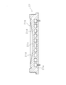
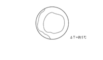
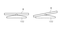
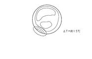
- FIG. 10 is an explanatory diagram showing the problems of the conventional sample stage.
- FIG. 10A schematically shows a conventional sample stage 102 on which a semiconductor wafer W is placed.
- FIG. 10B shows the measurement result of the temperature distribution in the semiconductor wafer W placed on the conventional sample stage 102 in the plasma environment.
- the contact surface has a shape in which a substantially central portion is convexly curved as shown in FIG. 10A.
- the semiconductor wafer W placed horizontally with respect to the suction plate is unstable because it is supported at one point as shown in the left diagram of FIG. 10A, and can easily be moved to one side as shown in the right diagram of FIG. 10A.
- a large gap is formed between the semiconductor wafer W and the suction plate on the other side.
- the thermal resistance of the portion having a large gap is locally increased, the amount of heat removal is reduced, and a local high temperature portion is generated in the semiconductor wafer W.
- a temperature difference ⁇ T of about 15 ° C. was detected in the semiconductor wafer W.
- the above-mentioned problem is generally generated not only when lapping is performed on the contact surface of the suction plate but also when the substantially central portion is curved in a convex shape as a result of performing a predetermined surface treatment. Is.
- Patent Document 1 since the sample stage described in Patent Document 1 has a configuration in which the semiconductor wafer and the sample stage are not in surface contact, it is difficult to control the temperature of the semiconductor wafer with high accuracy. Further, Patent Document 2 does not disclose means for solving the above-described problem.
- the present invention has been made in view of such circumstances, and even when the contact surface of the suction plate is subjected to a predetermined surface treatment, for example, lapping, by making the contact surface substantially concave, A sample stage capable of stably holding a substrate to be processed and a microwave plasma processing apparatus including the sample stage are provided.
- the sample stage according to the present invention has a contact surface that makes surface contact with the substrate to be processed in the sample stage that holds the substrate to be processed, and sucks the substrate to be processed that is in surface contact with the contact surface.
- a support substrate having a concave surface to which a non-contact surface of the suction plate is bonded, and the difference between the depth of the substantially central portion of the concave surface and the depth of the separated portion separated from the central portion is: It is characterized by being larger than the difference between the thickness of the suction plate at the part contacting the central portion and the thickness of the suction plate at the part contacting the separation part.
- the suction plate is bonded to the concave surface of the support substrate.
- the difference between the depth of the substantially central portion of the concave surface and the depth of the separated portion separated from the central portion is the thickness of the suction plate at the portion contacting the central portion and the suction plate at the portion contacting the separated portion. Therefore, even if the contact surface of the suction plate is subjected to a predetermined surface treatment and curved in a convex shape, the contact surface of the suction plate bonded to the concave surface is concave.
- the sample stage according to the present invention is characterized in that the concave surface of the support substrate has a flat bottom surface.
- the suction plate is more stably bonded to the support substrate than the concave surface formed in a mortar shape.
- the sample stage according to the present invention is characterized in that the concave surface of the support substrate has a trapezoidal cross section.
- the concave side surface has a trapezoidal shape
- the depth of the concave surface can be processed with higher accuracy than when the concave surface is processed into a spherical shape.
- the concave shape of the suction plate can be formed with high accuracy.
- the support substrate is made of an aluminum member, and includes a cooling water channel through which cooling water for cooling the substrate to be processed flows, and the suction plate is lapped on the contact surface.
- the ceramic member is provided with a heater for heating the substrate to be processed and an electrode for electrostatically adsorbing the substrate to be processed.
- the substrate to be processed can be cooled by passing a cooling liquid through the cooling water flow path. Further, the substrate to be processed can be heated by energizing the heater of the suction plate. Furthermore, the substrate to be processed can be electrostatically adsorbed by applying a direct current to the electrodes of the adsorption plate.
- a microwave plasma processing apparatus includes the above-described sample stage, and is configured to generate plasma in a processing chamber by microwaves and perform plasma processing on a substrate to be processed using the plasma.
- the substrate to be processed held on the sample stage can be uniformly plasma-processed.
- the substrate to be processed is stably held by making the contact surface substantially concave. And the substrate to be processed can be uniformly plasma-processed.
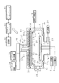
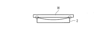
- FIG. 1 is a cross-sectional view schematically showing an example of a microwave plasma processing apparatus according to an embodiment of the present invention.
- the overall configuration of the microwave plasma processing apparatus will be described, and then the details of the sample stage 2 will be described.
- the microwave plasma processing apparatus is of, for example, an RLSA (Radial Line Slot Slot Antenna) type, and includes a substantially cylindrical processing chamber 1 that is airtight and grounded.
- the processing chamber 1 is made of, for example, aluminum, and includes a flat plate-shaped annular bottom wall 1a in which a circular opening 10 is formed in a substantially central portion, and a side wall provided around the bottom wall 1a. It is open.
- a cylindrical liner made of quartz may be provided on the inner periphery of the processing chamber 1.
- An annular gas introducing member 15 is provided on the side wall of the processing chamber 1, and a processing gas supply system 16 is connected to the gas introducing member 15.
- the gas introduction member 15 is arranged in a shower shape, for example.
- a predetermined processing gas is introduced from the processing gas supply system 16 into the processing chamber 1 through the gas introduction member 15.
- an appropriate gas is used according to the type of plasma processing.
- the sample stage 2 is preferably used for polysilicon (Poly-Si) etching processing that requires precise temperature control in order to perform high-precision processing.
- HBr gas, O2 gas, or the like is preferable. Used for.
- a gate valve 26 is provided on the side wall of the processing chamber 1.
- the bottom wall 1 a of the processing chamber 1 is provided with a bottomed cylindrical exhaust chamber 11 protruding downward so as to communicate with the opening 10.
- An exhaust pipe 23 is provided on the side wall of the exhaust chamber 11, and an exhaust device 24 including a high-speed vacuum pump is connected to the exhaust pipe 23.
- the gas in the processing chamber 1 is uniformly discharged into the space 11 a of the exhaust chamber 11 and is exhausted through the exhaust pipe 23. Therefore, the inside of the processing chamber 1 can be depressurized at a high speed to a predetermined degree of vacuum, for example, 0.133 Pa.
- a columnar member 3 made of ceramic such as AlN is projected substantially vertically at the center of the bottom of the exhaust chamber 11, and a semiconductor wafer W, which is a substrate to be processed, to be subjected to plasma processing is supported at the tip of the columnar member
- a sample stage 2 is provided.
- the sample stage 2 has a disc shape, and a guide ring 4 for guiding the semiconductor wafer W is provided on the outer edge thereof.
- the sample stage 2 is connected to a heater power source 6 for heating the semiconductor wafer W and a DC power source 8 for electrostatic adsorption.
- the sample table 2 is provided with wafer support pins (not shown) for supporting the semiconductor wafer W and raising and lowering it so as to protrude and retract with respect to the surface of the sample table 2. The detailed configuration of the sample stage 2 will be described later. Further, a high-frequency power source (not shown) for applying a bias to the semiconductor wafer W that is the substrate to be processed may be provided on the sample stage 2.
- the opening formed in the upper part of the processing chamber 1 is provided with a ring-shaped support 27 along the peripheral edge thereof.
- the support portion 27 is made of a dielectric material, for example, ceramic such as quartz or Al 2 ⁇ O 3 ⁇ , and is provided with a disk-shaped dielectric window 28 that allows microwaves to pass therethrough through a seal member 29.
- a disk-shaped slot plate 31 is provided above the dielectric window 28 so as to face the sample table 2.
- the slot plate 31 is locked to the upper end of the side wall of the processing chamber 1 while being in surface contact with the dielectric window 28.
- the slot plate 31 is made of a conductor, for example, a copper plate or an aluminum plate whose surface is gold-plated, and has a configuration in which a plurality of microwave radiation slots 32 are formed through a predetermined pattern. That is, the slot plate 31 constitutes an RLSA antenna.
- the microwave radiation slots 32 have, for example, a long groove shape, and are disposed close to each other so that a pair of adjacent microwave radiation slots 32 form a substantially L shape.
- the plurality of microwave radiation slots 32 forming a pair are arranged concentrically. Specifically, seven pairs of microwave radiation slots 32 are formed on the inner peripheral side and 26 pairs on the outer peripheral side. The length and arrangement interval of the microwave radiation slots 32 are determined according to the wavelength of the microwave and the like.
- dielectric plates 33 having a dielectric constant larger than that of vacuum are provided so as to be in surface contact with each other.
- the dielectric plate 33 has a flat dielectric disk portion.
- a hole is formed in a substantially central portion of the dielectric disk portion.
- a cylindrical microwave incident portion protrudes from the peripheral edge of the hole substantially perpendicular to the dielectric disk portion.
- a disc-shaped shield lid 34 is provided on the upper surface of the processing chamber 1 so as to cover the slot plate 31 and the dielectric plate 33.
- the shield lid 34 is made of a metal such as aluminum or stainless steel.
- a space between the upper surface of the processing chamber 1 and the shield lid 34 is sealed with a seal member 35.
- a lid-side cooling water channel 34a is formed inside the shield lid 34, and the slot plate 31, the dielectric window 28, and the dielectric plate 33 are made to flow through the lid-side cooling water channel 34a.
- the shield lid 34 is configured to be cooled.
- the shield lid 34 is grounded.
- An opening 36 is formed in the center of the upper wall of the shield lid 34, and a waveguide 37 is connected to the opening.
- the waveguide 37 has a circular cross-section coaxial waveguide 37a extending upward from the opening 36 of the shield lid 34, and a horizontal cross-section extending in the horizontal direction connected to the upper end of the coaxial waveguide 37a.
- the microwave generator 39 is connected to the end of the rectangular waveguide 37b via a matching circuit 38.
- a microwave generated by the microwave generator 39 for example, a microwave having a frequency of 2.45 GHz, is propagated to the slot plate 31 through the waveguide 37.
- the microwave frequency may be 8.35 GHz, 1.98 GHz, 915 MHz, or the like.
- a mode converter 40 is provided at the end of the rectangular waveguide 37b on the side where the coaxial waveguide 37a is connected.
- the coaxial waveguide 37 a has a cylindrical coaxial outer conductor 42 and a coaxial inner conductor 41 arranged along the center line of the coaxial outer conductor 42, and the lower end portion of the coaxial inner conductor 41 is a slot plate 31. Fixed in the center of the connection. The microwave incident portion of the dielectric plate 33 is fitted in the coaxial waveguide 37a.
- the microwave plasma processing apparatus includes a process controller 50 that controls each component of the microwave plasma processing apparatus.
- the process controller 50 includes a user interface 51 including a keyboard that allows a process manager to input commands to manage the microwave plasma processing apparatus, a display that visualizes and displays the operating status of the microwave plasma processing apparatus, and the like. Is connected.
- the process controller 50 also stores a control program for realizing various processes executed by the microwave plasma processing apparatus under the control of the process controller 50, a process control program in which process condition data and the like are recorded.
- the part 52 is connected.
- the process controller 50 calls and executes an arbitrary process control program according to an instruction from the user interface 51 from the storage unit 52, and performs desired processing in the microwave plasma processing apparatus under the control of the process controller 50. .
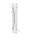
- FIG. 2 is a side sectional view schematically showing an example of the sample stage 2 according to the present embodiment
- FIGS. 3A and 3B are exploded side sectional views schematically showing an example of the sample stage 2.
- the sample stage 2 includes a support substrate 21 and a suction plate 23 bonded to the support substrate 21 with an adhesive 22.
- FIG. 4 is a side sectional view schematically showing an example of the support substrate 21.
- the support substrate 21 is made of an aluminum member, a stainless steel member, silicon carbide containing aluminum, or the like formed in a substantially disk shape having a larger diameter than the semiconductor wafer W, and a cooling water passage 21a is formed inside.
- the cooling water channel 21a cools the semiconductor wafer W by allowing cooling water to flow therethrough.
- a concave surface 21b having a circular shape in front view is formed on one end surface side (upper surface side) of the support substrate 21, an annular groove portion is formed on the radially outer side of the concave surface 21b, and an annular outer peripheral portion is formed on the outer side. Is formed.
- the concave surface 21b has a flat plate shape with a trapezoidal side cross section, and the depth of the concave surface 21b increases as the plan view formed in the substantially central portion is separated from the bottom surface portion 21c having a circular shape and radially outward from the bottom surface portion 21c. And a tapered portion 21d formed so as to be shallow. The difference between the depth of the central portion of the concave surface 21b and the depth of the tapered portion 21d spaced from the central portion is that the thickness of the suction plate 23 at the portion contacting the central portion and the tapered portion 21d are contacted as described later.
- the concave surface 21b has such a depth that the suction plate 23 becomes concave when the suction plate 23 is bonded to the concave surface 21b.
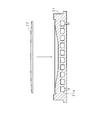
- FIG. 5 is an enlarged side cross-sectional view of a main part schematically showing an example of the suction plate 23.
- the suction plate 23 is made of a ceramic member having a disk shape that is substantially the same as or larger in diameter than the concave surface 21 b of the support substrate 21.
- the suction plate 23 includes a plate member 23a having a contact surface 23c that contacts and sucks the semiconductor wafer W and a non-contact surface 23b that is a surface opposite to the contact surface 23c.
- the contact surface 23c is embossed and the top of the embossed head is smoothed by lapping.
- the suction plate 23 subjected to the lapping process has a substantially central portion curved in a convex shape as compared with the outer peripheral portion.
- the non-contact surface 23 b is bonded to the concave surface 21 b of the support substrate 21 with an adhesive 22.
- the concave surface 21b of the support substrate 21 has a trapezoidal side cross section, but the adhesive 22 is infiltrated into the gap between the concave surface 21b and the suction plate 23, and the contact surface 23c of the suction plate 23 is a smoothly curved concave surface. It becomes a shape.
- the suction plate 23 is embedded with a heater 23e for superheating the semiconductor wafer W and an electrode 23d for electrostatically attracting the semiconductor wafer W.
- the heater 23e and the electrode 23d are each provided with a heater power source 6. And a DC power supply 8 are connected.
- the concave surface 21b and the concave shape of the suction plate 23 shown in FIGS. 2 to 5 are exaggerated, and the contact surface 23c of the suction plate 23 bonded to the support substrate 21 is infinitely flat. It is a concave shape close to.
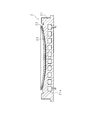
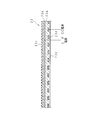
- FIG. 6 is an explanatory diagram for explaining the dimensions of the support substrate 21.
- the diameter ⁇ of the circular portion in which the concave surface 21b is formed on one end surface side of the support substrate 21 is, for example, 300 mm
- the diameter ⁇ of the bottom surface portion 21c of the concave surface 21b is 150 mm
- the depth D at the central portion of the concave surface 21b is about 20 to
- the angle formed by the bottom surface portion 21c and the tapered portion 21d is 25 ⁇ m, and ⁇ is 179.981 ° to 179.985 °.
- the values of the diameters ⁇ , ⁇ , the depth D, and the angle ⁇ are merely examples, and may be set as appropriate according to the dimensions and thickness of the semiconductor wafer W and the suction plate 23.
- setting the diameter ⁇ of the bottom surface portion 21c to 150 mm is more accurate than, for example, setting the diameter ⁇ to 100 mm. It has been confirmed that it can be processed.
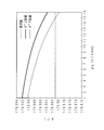
- FIG. 7 is a graph for explaining the dimensional shape of the concave surface 21 b formed on the support substrate 21.
- the horizontal axis is the diameter ⁇
- the vertical axis is the angle ⁇ .
- the reference value is the lower limit value of ⁇ when ⁇ is 150 mm.
- FIG. 8 is a graph showing the depth of the concave surface 21 b formed on the support substrate 21.
- the horizontal axis indicates the radial position of the concave surface 21b, and the vertical axis indicates the depth D.
- the plots of the square mark and the rhombus mark indicate the depth of the concave surface 21b that was cut separately, and it was confirmed that the concave surface 21b was formed with good reproducibility.
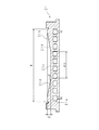
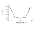
- FIG. 9 is an explanatory diagram for explaining the operation of the sample stage 2 according to the present embodiment.
- FIG. 9A schematically shows the sample stage 2 on which the semiconductor wafer W is placed, as in FIG.
- FIG. 9B shows the measurement result of the temperature distribution in the semiconductor wafer W placed on the sample stage 2 in the plasma environment.
- the contact surface 23c has a shape in which a substantially central portion is curved flat or concave. The concave shape shown in FIG.
- FIG. 9A is exaggerated and is actually a concave shape that is almost flat.
- the semiconductor wafer W placed horizontally with respect to the suction plate 23 is stably supported by the line, and as a result, as shown in FIG. 9B, the thermal resistance of the semiconductor wafer W becomes uniform.
- the temperature distribution of the semiconductor wafer W becomes uniform.
- the local temperature difference ⁇ T in the semiconductor wafer W could be suppressed to about 5 ° C.
- the semiconductor wafer W is stabilized by maintaining the smoothness of the contact surface 23c by lapping and making the contact surface 23c substantially concave. Can be retained.
- the suction plate 23 can be stably bonded to the support substrate 21 compared to the concave surface 21b in which the concave surface 21b is formed in a mortar shape. Can do. If the concave surface 21b is formed in a mortar shape, the central portion of the suction plate 23 may float and the suction plate 23 may be peeled off. However, when the concave surface 21b is formed in a trapezoidal side cross section, the peeling of the suction plate 23 is effectively suppressed. Can do.
- the concave surface 21b of the support substrate 21 has a trapezoidal side cross section, the depth of the concave surface 21b can be easily processed with high accuracy compared to the case of processing into an arc shape. As a result, the concave shape of the suction plate 23 can also be formed with high accuracy.
- the semiconductor wafer W can be brought into surface contact with the contact surface 23 c of the suction plate 23 by passing a direct current through the electrode 23 d embedded in the suction plate 23. Then, by energizing the heater 23 e with the semiconductor wafer W uniformly in surface contact with the suction plate 23, the semiconductor wafer W is overheated, and the cooling water is passed through the cooling water passage 21 a of the support substrate 21. The semiconductor wafer W can be cooled. Therefore, the temperature of the semiconductor wafer W can be uniformly controlled, and the semiconductor wafer W can be uniformly plasma processed.
- the shape of the concave surface shown in the embodiment is an example, and the shape is not limited.
- the concave surface may be formed in an arc shape.
- the concave surface may be formed in a mortar shape as long as the suction plate can be bonded to the support substrate.
- the semiconductor manufacturing apparatus to which the sample stage according to this embodiment is applied is not particularly limited, and is applicable to various processing apparatuses such as PVD, CVD, plasma CVD and other film forming processing apparatuses, and etching apparatuses. Can do.
Abstract
Description
また、上述の問題は、吸着板の接触面にラッピング加工を施した場合のみならず、所定の表面処理を施した結果、略中央部が凸状に湾曲するような場合、一般的に発生するものである。 FIG. 10 is an explanatory diagram showing the problems of the conventional sample stage. FIG. 10A schematically shows a
Moreover, the above-mentioned problem is generally generated not only when lapping is performed on the contact surface of the suction plate but also when the substantially central portion is curved in a convex shape as a result of performing a predetermined surface treatment. Is.
また、特許文献2には、上述の問題を解決する手段は開示されていない。 In addition, since the sample stage described in
Further,
また、処理室1の側壁には、マイクロ波プラズマ処理装置に隣接する搬送室(図示せず)との間で半導体ウエハWの搬入出を行うための搬入出口25と、この搬入出口25を開閉するゲートバルブ26とが設けられている。 An annular
Also, on the side wall of the
2 試料台
6 ヒータ電源
8 DC電源
21 支持基板
21a 冷却水流路
21b 凹面
21c 底面部
21d テーパ部
22 接着剤
23 吸着板
23a 板部材
23b 非接触面
23c 接触面
23d 電極
23e ヒータ
W 半導体ウエハ DESCRIPTION OF
Claims (5)
- 基板処理が施されるべき被処理基板を保持する試料台において、
被処理基板が面接触する接触面を有し、該接触面に面接触した被処理基板を吸着する吸着板と、
該吸着板の非接触面が接着された凹面を有する支持基板と
を備え、
前記凹面の略中央部の深さと、該中央部から離隔した離隔部位の深さとの差は、該中央部に接触する部位における前記吸着板の厚みと、前記離隔部位に接触する部位における前記吸着板の厚みとの差よりも大きい
ことを特徴とする試料台。 In a sample stage for holding a substrate to be processed to be processed,
A suction plate that has a contact surface that makes surface contact with the substrate to be processed, and that sucks the substrate to be processed that is in surface contact with the contact surface;
A support substrate having a concave surface to which the non-contact surface of the suction plate is bonded,
The difference between the depth of the substantially central portion of the concave surface and the depth of the separated portion separated from the central portion is the thickness of the suction plate at the portion contacting the central portion and the adsorption at the portion contacting the separated portion. A sample stage characterized by being larger than the difference from the thickness of the plate. - 前記支持基板の凹面は、平坦な底面部を有する
ことを特徴とする請求項1に記載の試料台。 The sample stage according to claim 1, wherein the concave surface of the support substrate has a flat bottom surface portion. - 前記支持基板の凹面は、側断面が台形状である
ことを特徴とする請求項1又は請求項2に記載の試料台。 The sample table according to claim 1 or 2, wherein the concave surface of the support substrate has a trapezoidal cross section. - 前記支持基板は、
アルミニウム部材からなり、被処理基板を冷却するための冷却水が通流する冷却水流路を備え、
前記吸着板は、
前記接触面にラッピング加工が施されたセラミック部材からなり、被処理基板を加熱するためのヒータと、被処理基板を静電吸着するための電極とを該セラミック部材の内部に備える
ことを特徴とする請求項1乃至請求項3のいずれか一つに記載の試料台。 The support substrate is
It is made of an aluminum member and includes a cooling water flow path through which cooling water for cooling the substrate to be processed flows.
The suction plate is
The ceramic member is provided with a lapping process on the contact surface, and includes a heater for heating the substrate to be processed and an electrode for electrostatically adsorbing the substrate to be processed. The sample stage according to any one of claims 1 to 3. - 請求項1乃至請求項4のいずれか一つに記載の試料台を備え、マイクロ波によって処理室内にプラズマを生成し、該プラズマにて被処理基板にプラズマ処理を施すように構成してある
ことを特徴とするマイクロ波プラズマ処理装置。 A sample stage according to any one of claims 1 to 4 is provided, wherein plasma is generated in a processing chamber by microwaves, and the substrate is processed with the plasma. A microwave plasma processing apparatus.
Priority Applications (4)
| Application Number | Priority Date | Filing Date | Title |
|---|---|---|---|
| KR1020127010099A KR101324589B1 (en) | 2009-10-20 | 2010-09-29 | Sample table and microwave plasma processing apparatus |
| US13/502,829 US20120211165A1 (en) | 2009-10-20 | 2010-09-29 | Sample table and microwave plasma processing apparatus |
| CN201080047610.7A CN102576673B (en) | 2009-10-20 | 2010-09-29 | Sample bench and microwave plasma processing apparatus |
| US15/966,506 US10896842B2 (en) | 2009-10-20 | 2018-04-30 | Manufacturing method of sample table |
Applications Claiming Priority (2)
| Application Number | Priority Date | Filing Date | Title |
|---|---|---|---|
| JP2009241538A JP5628507B2 (en) | 2009-10-20 | 2009-10-20 | Sample stage and microwave plasma processing equipment |
| JP2009-241538 | 2009-10-20 |
Related Child Applications (2)
| Application Number | Title | Priority Date | Filing Date |
|---|---|---|---|
| US13/502,829 A-371-Of-International US20120211165A1 (en) | 2009-10-20 | 2010-09-29 | Sample table and microwave plasma processing apparatus |
| US15/966,506 Continuation-In-Part US10896842B2 (en) | 2009-10-20 | 2018-04-30 | Manufacturing method of sample table |
Publications (1)
| Publication Number | Publication Date |
|---|---|
| WO2011048917A1 true WO2011048917A1 (en) | 2011-04-28 |
Family
ID=43900155
Family Applications (1)
| Application Number | Title | Priority Date | Filing Date |
|---|---|---|---|
| PCT/JP2010/066910 WO2011048917A1 (en) | 2009-10-20 | 2010-09-29 | Sample table and microwave plasma processing apparatus |
Country Status (6)
| Country | Link |
|---|---|
| US (1) | US20120211165A1 (en) |
| JP (1) | JP5628507B2 (en) |
| KR (1) | KR101324589B1 (en) |
| CN (1) | CN102576673B (en) |
| TW (1) | TWI459502B (en) |
| WO (1) | WO2011048917A1 (en) |
Families Citing this family (5)
| Publication number | Priority date | Publication date | Assignee | Title |
|---|---|---|---|---|
| WO2014024216A1 (en) * | 2012-08-06 | 2014-02-13 | パイオニア株式会社 | Dry etching device and dry etching method |
| JP6741548B2 (en) * | 2016-10-14 | 2020-08-19 | 日本碍子株式会社 | Member for semiconductor manufacturing apparatus and manufacturing method thereof |
| US10510512B2 (en) * | 2018-01-25 | 2019-12-17 | Tokyo Electron Limited | Methods and systems for controlling plasma performance |
| CN110983298A (en) * | 2019-12-24 | 2020-04-10 | 中国科学院半导体研究所 | Sample table structure for microwave plasma chemical vapor deposition device |
| KR20220086013A (en) | 2020-12-16 | 2022-06-23 | 삼성전자주식회사 | Semiconductor processing equipment including electrostatic chuck for plasma processing |
Citations (4)
| Publication number | Priority date | Publication date | Assignee | Title |
|---|---|---|---|---|
| JP2004273619A (en) * | 2003-03-06 | 2004-09-30 | Hitachi High-Technologies Corp | Test piece setting device for vacuum processing apparatus |
| JP2006013302A (en) * | 2004-06-29 | 2006-01-12 | Ngk Insulators Ltd | Substrate mounting device and substrate temperature adjusting method |
| JP2008042138A (en) * | 2006-08-10 | 2008-02-21 | Tokyo Electron Ltd | Electrostatic chuck device |
| JP2009510774A (en) * | 2005-09-30 | 2009-03-12 | ラム リサーチ コーポレーション | Electrostatic chuck assembly comprising a dielectric material and / or cavity having varying thickness, profile and / or shape, method of use thereof, and apparatus incorporating the same |
Family Cites Families (11)
| Publication number | Priority date | Publication date | Assignee | Title |
|---|---|---|---|---|
| US5886863A (en) * | 1995-05-09 | 1999-03-23 | Kyocera Corporation | Wafer support member |
| US5761023A (en) * | 1996-04-25 | 1998-06-02 | Applied Materials, Inc. | Substrate support with pressure zones having reduced contact area and temperature feedback |
| US6177023B1 (en) * | 1997-07-11 | 2001-01-23 | Applied Komatsu Technology, Inc. | Method and apparatus for electrostatically maintaining substrate flatness |
| US6228438B1 (en) * | 1999-08-10 | 2001-05-08 | Unakis Balzers Aktiengesellschaft | Plasma reactor for the treatment of large size substrates |
| JP3650025B2 (en) * | 2000-12-04 | 2005-05-18 | シャープ株式会社 | Plasma process equipment |
| GB0029570D0 (en) * | 2000-12-05 | 2001-01-17 | Trikon Holdings Ltd | Electrostatic clamp |
| US7651571B2 (en) * | 2005-12-22 | 2010-01-26 | Kyocera Corporation | Susceptor |
| US8284538B2 (en) * | 2006-08-10 | 2012-10-09 | Tokyo Electron Limited | Electrostatic chuck device |
| US20080041312A1 (en) * | 2006-08-10 | 2008-02-21 | Shoichiro Matsuyama | Stage for plasma processing apparatus, and plasma processing apparatus |
| US7619870B2 (en) * | 2006-08-10 | 2009-11-17 | Tokyo Electron Limited | Electrostatic chuck |
| JP5029089B2 (en) * | 2007-03-26 | 2012-09-19 | 東京エレクトロン株式会社 | Mounting table for plasma processing apparatus and plasma processing apparatus |
-
2009
- 2009-10-20 JP JP2009241538A patent/JP5628507B2/en active Active
-
2010
- 2010-09-29 CN CN201080047610.7A patent/CN102576673B/en active Active
- 2010-09-29 US US13/502,829 patent/US20120211165A1/en not_active Abandoned
- 2010-09-29 KR KR1020127010099A patent/KR101324589B1/en active IP Right Grant
- 2010-09-29 WO PCT/JP2010/066910 patent/WO2011048917A1/en active Application Filing
- 2010-10-19 TW TW099135496A patent/TWI459502B/en active
Patent Citations (4)
| Publication number | Priority date | Publication date | Assignee | Title |
|---|---|---|---|---|
| JP2004273619A (en) * | 2003-03-06 | 2004-09-30 | Hitachi High-Technologies Corp | Test piece setting device for vacuum processing apparatus |
| JP2006013302A (en) * | 2004-06-29 | 2006-01-12 | Ngk Insulators Ltd | Substrate mounting device and substrate temperature adjusting method |
| JP2009510774A (en) * | 2005-09-30 | 2009-03-12 | ラム リサーチ コーポレーション | Electrostatic chuck assembly comprising a dielectric material and / or cavity having varying thickness, profile and / or shape, method of use thereof, and apparatus incorporating the same |
| JP2008042138A (en) * | 2006-08-10 | 2008-02-21 | Tokyo Electron Ltd | Electrostatic chuck device |
Also Published As
| Publication number | Publication date |
|---|---|
| US20120211165A1 (en) | 2012-08-23 |
| TW201133699A (en) | 2011-10-01 |
| KR20120060889A (en) | 2012-06-12 |
| KR101324589B1 (en) | 2013-11-01 |
| TWI459502B (en) | 2014-11-01 |
| CN102576673A (en) | 2012-07-11 |
| JP2011091096A (en) | 2011-05-06 |
| JP5628507B2 (en) | 2014-11-19 |
| CN102576673B (en) | 2015-08-19 |
Similar Documents
| Publication | Publication Date | Title |
|---|---|---|
| JP6452449B2 (en) | Mounting table and substrate processing apparatus | |
| KR102455673B1 (en) | Focus ring and substrate processing apparatus | |
| US8636871B2 (en) | Plasma processing apparatus, plasma processing method and storage medium | |
| JP5893516B2 (en) | Processing apparatus for processing object and mounting table for processing object | |
| JP2010118549A (en) | Plasma etching method and plasma etching device | |
| TW201923953A (en) | Single wafer processing environments with spatial separation | |
| JP5628507B2 (en) | Sample stage and microwave plasma processing equipment | |
| JP2019176030A (en) | Plasma processing apparatus | |
| TWI794428B (en) | Workpiece placement apparatus and processing apparatus | |
| KR101898079B1 (en) | Plasma processing apparatus | |
| JP2019041024A (en) | Member with flow channel for refrigerant and control method therefor, and substrate processing apparatus | |
| KR20210102075A (en) | Stage, plasma processing apparatus, and cleaning method | |
| TWI809007B (en) | Focus ring for semiconductor manufacturing apparatus and semiconductor manufacturing apparatus | |
| US10896842B2 (en) | Manufacturing method of sample table | |
| JP5479013B2 (en) | Plasma processing apparatus and slow wave plate used therefor | |
| US11538669B2 (en) | Plasma processing apparatus | |
| JP5927260B2 (en) | Sample stage and microwave plasma processing equipment | |
| JP5859792B2 (en) | Plasma etching method | |
| US11201039B2 (en) | Mounting apparatus for object to be processed and processing apparatus | |
| TW202032715A (en) | Placing table and substrate processing apparatus | |
| JP2010010231A (en) | Plasma treatment device | |
| JP7204564B2 (en) | Plasma processing equipment | |
| JP5728565B2 (en) | Plasma processing apparatus and slow wave plate used therefor | |
| WO2022202364A1 (en) | Semiconductor manufacturing apparatus and component for semiconductor manufacturing apparatus | |
| KR101749311B1 (en) | Substrate supporting unit and apparatus for treating substrate including the same |
Legal Events
| Date | Code | Title | Description |
|---|---|---|---|
| WWE | Wipo information: entry into national phase |
Ref document number: 201080047610.7 Country of ref document: CN |
|
| 121 | Ep: the epo has been informed by wipo that ep was designated in this application |
Ref document number: 10824766 Country of ref document: EP Kind code of ref document: A1 |
|
| ENP | Entry into the national phase |
Ref document number: 20127010099 Country of ref document: KR Kind code of ref document: A |
|
| WWE | Wipo information: entry into national phase |
Ref document number: 13502829 Country of ref document: US |
|
| 122 | Ep: pct application non-entry in european phase |
Ref document number: 10824766 Country of ref document: EP Kind code of ref document: A1 |