KR101324589B1 - Sample table and microwave plasma processing apparatus - Google Patents
Sample table and microwave plasma processing apparatus Download PDFInfo
- Publication number
- KR101324589B1 KR101324589B1 KR1020127010099A KR20127010099A KR101324589B1 KR 101324589 B1 KR101324589 B1 KR 101324589B1 KR 1020127010099 A KR1020127010099 A KR 1020127010099A KR 20127010099 A KR20127010099 A KR 20127010099A KR 101324589 B1 KR101324589 B1 KR 101324589B1
- Authority
- KR
- South Korea
- Prior art keywords
- substrate
- semiconductor wafer
- concave surface
- contact surface
- support substrate
- Prior art date
Links
- 238000012545 processing Methods 0.000 title claims abstract description 41
- 239000000758 substrate Substances 0.000 claims abstract description 68
- 238000001179 sorption measurement Methods 0.000 claims abstract description 52
- 238000000034 method Methods 0.000 claims description 29
- 239000000498 cooling water Substances 0.000 claims description 12
- 239000000919 ceramic Substances 0.000 claims description 9
- 229910052782 aluminium Inorganic materials 0.000 claims description 7
- XAGFODPZIPBFFR-UHFFFAOYSA-N aluminium Chemical compound [Al] XAGFODPZIPBFFR-UHFFFAOYSA-N 0.000 claims description 7
- 238000010438 heat treatment Methods 0.000 claims description 4
- 238000001816 cooling Methods 0.000 claims description 3
- 238000000926 separation method Methods 0.000 claims 2
- 239000004065 semiconductor Substances 0.000 abstract description 51
- 238000009832 plasma treatment Methods 0.000 abstract description 4
- 229910052721 tungsten Inorganic materials 0.000 abstract description 2
- 238000010586 diagram Methods 0.000 description 6
- 230000005855 radiation Effects 0.000 description 6
- 239000004020 conductor Substances 0.000 description 5
- 238000009826 distribution Methods 0.000 description 5
- 239000000853 adhesive Substances 0.000 description 4
- 238000004381 surface treatment Methods 0.000 description 4
- 230000001070 adhesive effect Effects 0.000 description 3
- 230000002093 peripheral effect Effects 0.000 description 3
- 238000004049 embossing Methods 0.000 description 2
- 238000005530 etching Methods 0.000 description 2
- 238000002474 experimental method Methods 0.000 description 2
- 238000004519 manufacturing process Methods 0.000 description 2
- 238000005259 measurement Methods 0.000 description 2
- 238000013021 overheating Methods 0.000 description 2
- 230000003647 oxidation Effects 0.000 description 2
- 238000007254 oxidation reaction Methods 0.000 description 2
- 229910021420 polycrystalline silicon Inorganic materials 0.000 description 2
- 229920005591 polysilicon Polymers 0.000 description 2
- 239000010453 quartz Substances 0.000 description 2
- VYPSYNLAJGMNEJ-UHFFFAOYSA-N silicon dioxide Inorganic materials O=[Si]=O VYPSYNLAJGMNEJ-UHFFFAOYSA-N 0.000 description 2
- 238000003860 storage Methods 0.000 description 2
- QNRATNLHPGXHMA-XZHTYLCXSA-N (r)-(6-ethoxyquinolin-4-yl)-[(2s,4s,5r)-5-ethyl-1-azabicyclo[2.2.2]octan-2-yl]methanol;hydrochloride Chemical compound Cl.C([C@H]([C@H](C1)CC)C2)CN1[C@@H]2[C@H](O)C1=CC=NC2=CC=C(OCC)C=C21 QNRATNLHPGXHMA-XZHTYLCXSA-N 0.000 description 1
- 229910018072 Al 2 O 3 Inorganic materials 0.000 description 1
- RYGMFSIKBFXOCR-UHFFFAOYSA-N Copper Chemical compound [Cu] RYGMFSIKBFXOCR-UHFFFAOYSA-N 0.000 description 1
- 239000002826 coolant Substances 0.000 description 1
- 229910052802 copper Inorganic materials 0.000 description 1
- 239000010949 copper Substances 0.000 description 1
- 238000005520 cutting process Methods 0.000 description 1
- 230000003247 decreasing effect Effects 0.000 description 1
- 230000003028 elevating effect Effects 0.000 description 1
- 239000007788 liquid Substances 0.000 description 1
- 238000003754 machining Methods 0.000 description 1
- 229910052751 metal Inorganic materials 0.000 description 1
- 239000002184 metal Substances 0.000 description 1
- 230000000149 penetrating effect Effects 0.000 description 1
- 239000012466 permeate Substances 0.000 description 1
- 238000005268 plasma chemical vapour deposition Methods 0.000 description 1
- 230000000644 propagated effect Effects 0.000 description 1
- 230000000717 retained effect Effects 0.000 description 1
- HBMJWWWQQXIZIP-UHFFFAOYSA-N silicon carbide Chemical compound [Si+]#[C-] HBMJWWWQQXIZIP-UHFFFAOYSA-N 0.000 description 1
- 229910010271 silicon carbide Inorganic materials 0.000 description 1
- 229910001220 stainless steel Inorganic materials 0.000 description 1
- 239000010935 stainless steel Substances 0.000 description 1
- 238000012546 transfer Methods 0.000 description 1
- 230000001960 triggered effect Effects 0.000 description 1
- WFKWXMTUELFFGS-UHFFFAOYSA-N tungsten Chemical compound [W] WFKWXMTUELFFGS-UHFFFAOYSA-N 0.000 description 1
- 239000010937 tungsten Substances 0.000 description 1
Images


Classifications
-
- H—ELECTRICITY
- H01—ELECTRIC ELEMENTS
- H01L—SEMICONDUCTOR DEVICES NOT COVERED BY CLASS H10
- H01L21/00—Processes or apparatus adapted for the manufacture or treatment of semiconductor or solid state devices or of parts thereof
- H01L21/67—Apparatus specially adapted for handling semiconductor or electric solid state devices during manufacture or treatment thereof; Apparatus specially adapted for handling wafers during manufacture or treatment of semiconductor or electric solid state devices or components ; Apparatus not specifically provided for elsewhere
- H01L21/683—Apparatus specially adapted for handling semiconductor or electric solid state devices during manufacture or treatment thereof; Apparatus specially adapted for handling wafers during manufacture or treatment of semiconductor or electric solid state devices or components ; Apparatus not specifically provided for elsewhere for supporting or gripping
- H01L21/687—Apparatus specially adapted for handling semiconductor or electric solid state devices during manufacture or treatment thereof; Apparatus specially adapted for handling wafers during manufacture or treatment of semiconductor or electric solid state devices or components ; Apparatus not specifically provided for elsewhere for supporting or gripping using mechanical means, e.g. chucks, clamps or pinches
- H01L21/68714—Apparatus specially adapted for handling semiconductor or electric solid state devices during manufacture or treatment thereof; Apparatus specially adapted for handling wafers during manufacture or treatment of semiconductor or electric solid state devices or components ; Apparatus not specifically provided for elsewhere for supporting or gripping using mechanical means, e.g. chucks, clamps or pinches the wafers being placed on a susceptor, stage or support
- H01L21/68735—Apparatus specially adapted for handling semiconductor or electric solid state devices during manufacture or treatment thereof; Apparatus specially adapted for handling wafers during manufacture or treatment of semiconductor or electric solid state devices or components ; Apparatus not specifically provided for elsewhere for supporting or gripping using mechanical means, e.g. chucks, clamps or pinches the wafers being placed on a susceptor, stage or support characterised by edge profile or support profile
-
- H—ELECTRICITY
- H01—ELECTRIC ELEMENTS
- H01L—SEMICONDUCTOR DEVICES NOT COVERED BY CLASS H10
- H01L21/00—Processes or apparatus adapted for the manufacture or treatment of semiconductor or solid state devices or of parts thereof
- H01L21/02—Manufacture or treatment of semiconductor devices or of parts thereof
- H01L21/04—Manufacture or treatment of semiconductor devices or of parts thereof the devices having at least one potential-jump barrier or surface barrier, e.g. PN junction, depletion layer or carrier concentration layer
- H01L21/18—Manufacture or treatment of semiconductor devices or of parts thereof the devices having at least one potential-jump barrier or surface barrier, e.g. PN junction, depletion layer or carrier concentration layer the devices having semiconductor bodies comprising elements of Group IV of the Periodic System or AIIIBV compounds with or without impurities, e.g. doping materials
- H01L21/30—Treatment of semiconductor bodies using processes or apparatus not provided for in groups H01L21/20 - H01L21/26
- H01L21/302—Treatment of semiconductor bodies using processes or apparatus not provided for in groups H01L21/20 - H01L21/26 to change their surface-physical characteristics or shape, e.g. etching, polishing, cutting
- H01L21/306—Chemical or electrical treatment, e.g. electrolytic etching
- H01L21/3065—Plasma etching; Reactive-ion etching
-
- H—ELECTRICITY
- H01—ELECTRIC ELEMENTS
- H01L—SEMICONDUCTOR DEVICES NOT COVERED BY CLASS H10
- H01L21/00—Processes or apparatus adapted for the manufacture or treatment of semiconductor or solid state devices or of parts thereof
- H01L21/67—Apparatus specially adapted for handling semiconductor or electric solid state devices during manufacture or treatment thereof; Apparatus specially adapted for handling wafers during manufacture or treatment of semiconductor or electric solid state devices or components ; Apparatus not specifically provided for elsewhere
- H01L21/683—Apparatus specially adapted for handling semiconductor or electric solid state devices during manufacture or treatment thereof; Apparatus specially adapted for handling wafers during manufacture or treatment of semiconductor or electric solid state devices or components ; Apparatus not specifically provided for elsewhere for supporting or gripping
- H01L21/687—Apparatus specially adapted for handling semiconductor or electric solid state devices during manufacture or treatment thereof; Apparatus specially adapted for handling wafers during manufacture or treatment of semiconductor or electric solid state devices or components ; Apparatus not specifically provided for elsewhere for supporting or gripping using mechanical means, e.g. chucks, clamps or pinches
- H01L21/68714—Apparatus specially adapted for handling semiconductor or electric solid state devices during manufacture or treatment thereof; Apparatus specially adapted for handling wafers during manufacture or treatment of semiconductor or electric solid state devices or components ; Apparatus not specifically provided for elsewhere for supporting or gripping using mechanical means, e.g. chucks, clamps or pinches the wafers being placed on a susceptor, stage or support
- H01L21/6875—Apparatus specially adapted for handling semiconductor or electric solid state devices during manufacture or treatment thereof; Apparatus specially adapted for handling wafers during manufacture or treatment of semiconductor or electric solid state devices or components ; Apparatus not specifically provided for elsewhere for supporting or gripping using mechanical means, e.g. chucks, clamps or pinches the wafers being placed on a susceptor, stage or support characterised by a plurality of individual support members, e.g. support posts or protrusions
Abstract
랩핑 가공에 의해 접촉면의 평활성을 유지하고, 그리고 접촉면을 대략 오목 형상으로 함으로써, 반도체 웨이퍼를 안정적으로 보유지지(holding)할 수 있는 시료대 및 당해 시료대를 구비한 마이크로파 플라즈마 처리 장치를 제공한다. 플라즈마 처리가 행해질 반도체 웨이퍼(W)를 보유지지하는 시료대(2)에 있어서, 랩핑 가공이 행해져 있고, 반도체 웨이퍼(W)가 면접촉하는 접촉면을 갖고, 당해 접촉면에 면접촉한 반도체 웨이퍼(W)를 흡착하는 흡착판과, 당해 흡착판의 비접촉면이 접착된 오목면을 갖는 지지 기판을 구비하고, 상기 오목면의 대략 중앙부의 깊이와, 당해 중앙부로부터 이격된 이격 부위의 깊이와의 차이는, 당해 중앙부에 접촉하는 부위에 있어서의 상기 흡착판의 두께와, 상기 이격 부위에 접촉하는 부위에 있어서의 상기 흡착판의 두께와의 차이보다도 크게 구성한다. 또한, 시료대(2)를 마이크로파 플라즈마 처리 장치에 구비한다.Provided are a sample stand capable of stably holding a semiconductor wafer and a microwave plasma processing apparatus provided with the sample stand by maintaining the smoothness of the contact surface by lapping and making the contact surface substantially concave. In the sample stage 2 holding the semiconductor wafer W to be subjected to the plasma treatment, lapping is performed, the semiconductor wafer W having a contact surface in surface contact with the semiconductor wafer W, and in surface contact with the contact surface. And a support substrate having a concave surface to which a non-contact surface of the adsorption plate is bonded, wherein the difference between the depth of the center portion of the concave surface and the depth of the spaced apart portion from the center portion is different from the center portion. It consists of larger than the difference of the thickness of the said adsorption plate in the site | part which contacts to and the thickness of the said adsorption board in the site | part which contacts the said space | part spacing. In addition, the sample stage 2 is provided in the microwave plasma processing apparatus.

Description
본 발명은, 기판 처리가 행해질 피(被)처리 기판을 보유지지(holding)하는 시료대 및, 당해 시료대를 구비하고, 마이크로파에 의해 처리실 내에 플라즈마를 생성하여, 당해 플라즈마로 피처리 기판에 플라즈마 처리를 행하도록 구성된 마이크로파 플라즈마 처리 장치에 관한 것이다.The present invention includes a sample stage holding a substrate to be subjected to substrate treatment, and the sample stage, and generates plasma in the processing chamber by microwaves, and plasma is generated on the substrate to be processed by the plasma. A microwave plasma processing apparatus configured to perform a process.
반도체 제조 장치는, 플라즈마 처리가 행해질 피처리 기판, 예를 들면 반도체 웨이퍼를 흡착 보유지지하는 시료대를 구비한다. 시료대는, 반도체 웨이퍼를 정전 흡착하는 세라믹제의 흡착판을 구비하고 있고, 당해 흡착판 내부에는, 정전 흡착을 위한 전극, 가열용의 히터 등이 매설되어 있다. 반도체 웨이퍼를 균일하게 처리하기 위해서는, 당해 반도체 웨이퍼의 온도 분포를 균일하게 할 필요가 있다. 이 때문에, 반도체 웨이퍼에 접촉하는 흡착판의 접촉면은, 당해 접촉면 및 반도체 웨이퍼 간의 열저항이 균일하게 되도록, 랩핑(lapping) 가공에 의해 평활화되어 있다.The semiconductor manufacturing apparatus is provided with the sample stand which adsorbs-holds the to-be-processed board | substrate to which a plasma process will be performed, for example, a semiconductor wafer. The sample stage includes a ceramic adsorption plate for electrostatically adsorbing a semiconductor wafer. An electrode for electrostatic adsorption, a heater for heating, and the like are embedded in the adsorption plate. In order to process a semiconductor wafer uniformly, it is necessary to make the temperature distribution of the said semiconductor wafer uniform. For this reason, the contact surface of the adsorption plate which contacts a semiconductor wafer is smoothed by the lapping process so that the heat resistance between the said contact surface and a semiconductor wafer may become uniform.
한편, 특허문헌 1에는, 반도체 웨이퍼를 지지하는 기판 지지면에 오목부를 형성하여, 반도체 웨이퍼와, 기판 지지면과의 사이에 소정의 공간이 형성되도록 구성된 시료대가 개시되어 있다. 당해 시료대는, 반도체 웨이퍼의 중앙부에서 온도가 상승하기 쉬운 바, 오목부의 중앙부에서 깊이가 가장 크고, 중앙으로부터 단부(端部)를 향하여 얕아지도록 형성함으로써, 반도체 웨이퍼의 온도 분포를 균일하게 하는 것을 목적으로 한 것이다.On the other hand,
특허문헌 2에는, 판 형상 세라믹체의 한쪽의 주면(主面)에, 그 외주부(外周部)를 남기고 깊이가 3∼10㎛의 오목부를 형성하고, 상기 외주부 정면(頂面)에 있어서의 기복을 1∼3㎛로 함과 함께, 상기 오목부 저면의 주연부에 가스 홈을 설치하고, 상기 오목부 저면 하방의 판 형상 세라믹체 중에 정전 흡착용 전극을 배치하여 구성된 시료대가 개시되어 있다.In
도 10은, 종래의 시료대가 갖는 문제점을 나타내는 설명도이다. 도 10(a)는, 반도체 웨이퍼(W)가 올려놓여진 종래의 시료대(102)를 개략적으로 나타내고 있다. 도 10(b)는, 플라즈마 환경하에 있어서, 종래의 시료대(102)에 올려놓여진 반도체 웨이퍼(W)에 있어서의 온도 분포의 측정 결과를 나타내고 있다. 시료대에 설치된 흡착판의 접촉면을 평활하게 하기 위해 랩핑 가공을 행한 경우, 접촉면은 도 10(a)에 나타내는 바와 같이, 대략 중앙부가 볼록 형상으로 만곡된 형상이 된다. 이 때문에, 흡착판에 대하여 수평으로 올려놓여진 반도체 웨이퍼(W)는, 도 10(a) 왼쪽 도면에 나타내는 바와 같이, 일점 지지되기 때문에, 불안정하고, 도 10(a) 오른쪽 도면에 나타내는 바와 같이 쉽게 편측으로 기울어져, 다른 편측에는 반도체 웨이퍼(W)와, 흡착판과의 사이에 큰 간극이 발생한다. 결과적으로, 도 10(b)에 나타내는 바와 같이, 간극이 큰 개소의 열저항이 국소적으로 높아지고, 발열량이 감소하여, 반도체 웨이퍼(W)에 국소 고온 부위가 발생한다. 어느 실험에 의하면, 반도체 웨이퍼(W)에 있어서 약 15℃의 온도차(ΔT)가 검출되었다. It is explanatory drawing which shows the problem with the conventional sample stand. 10 (a) schematically shows a
또한, 전술한 문제는, 흡착판의 접촉면에 랩핑 가공을 행한 경우뿐만 아니라, 소정의 표면 처리를 행한 결과, 대략 중앙부가 볼록 형상으로 만곡되는 바와 같은 경우, 일반적으로 발생하는 것이다.In addition, the above-mentioned problem generally occurs not only when the lapping process is performed on the contact surface of a suction plate, but also when the center part curves in convex shape as a result of performing predetermined surface treatment.
또한, 특허문헌 1에 기재된 시료대는, 반도체 웨이퍼와, 시료대가 면접촉하지 않는 구성이기 때문에, 반도체 웨이퍼의 온도를 고정밀도로 제어하는 것은 곤란하다.In addition, since the sample stand described in
또한, 특허문헌 2에는, 전술한 문제를 해결하는 수단은 개시되어 있지 않다.In addition,
본 발명은 이러한 사정을 감안하여 이루어진 것으로, 흡착판의 접촉면에 소정의 표면 처리, 예를 들면 랩핑 가공을 행한 경우라도, 당해 접촉면을 대략 오목 형상으로 함으로써, 피처리 기판을 안정적으로 보유지지할 수 있는 시료대 및 당해 시료대를 구비한 마이크로파 플라즈마 처리 장치를 제공한다.This invention is made | formed in view of such a situation, Even if a predetermined surface treatment, for example lapping process, is performed to the contact surface of an adsorption plate, by making the said contact surface into substantially concave shape, it can hold | maintain a to-be-processed substrate stably. Provided are a sample stage and a microwave plasma processing apparatus including the sample stage.
본 발명에 따른 시료대는, 기판 처리가 행해질 피처리 기판을 보유지지하는 시료대에 있어서, 피처리 기판이 면접촉하는 접촉면을 갖고, 당해 접촉면에 면접촉한 피처리 기판을 흡착하는 흡착판과, 당해 흡착판의 비접촉면이 접착된 오목면을 갖는 지지 기판을 구비하고, 상기 오목면의 대략 중앙부의 깊이와, 당해 중앙부로부터 이격된 이격 부위의 깊이와의 차이는, 당해 중앙부에 접촉하는 부위에 있어서의 상기 흡착판의 두께와, 상기 이격 부위에 접촉하는 부위에 있어서의 상기 흡착판의 두께와의 차이보다도 큰 것을 특징으로 한다.The sample stage according to the present invention is a sample stage for holding a substrate to be subjected to substrate treatment, the sample stage having a contact surface to which the substrate is subjected to surface contact, and an adsorption plate for adsorbing the substrate to be subjected to surface contact with the contact surface; And a support substrate having a concave surface to which a non-contact surface of is bonded, wherein a difference between the depth of the substantially center portion of the concave surface and the depth of the spaced apart portion spaced from the center portion is determined in the region in contact with the center portion. It is larger than the difference between the thickness of an adsorption plate, and the thickness of the said adsorption plate in the site | part which contact | connects the said space | part spacing. It is characterized by the above-mentioned.
본 발명에 있어서는, 흡착판이 지지 기판의 오목면에 접착되어 있다. 그리고, 당해 오목면의 대략 중앙부의 깊이와, 당해 중앙부로부터 이격된 이격 부위의 깊이와의 차이는, 당해 중앙부에 접촉하는 부위에 있어서의 흡착판의 두께와, 이격 부위에 접촉하는 부위에 있어서의 흡착판의 두께와의 차이보다도 크기 때문에, 흡착판의 접촉면에 소정의 표면 처리가 행해져 볼록 형상으로 만곡된 경우라도, 오목면에 접착된 흡착판의 접촉면은 오목 형상이다.In the present invention, the adsorption plate is adhered to the concave surface of the support substrate. And the difference between the depth of the substantially center part of the said concave surface, and the depth of the space | part spaced apart from the said center part is the thickness of the adsorption plate in the site | part which contacts the said center part, and the adsorption plate in the site | part which contacts a spaced part. Since the contact surface of the adsorption plate is bent in a convex shape because a predetermined surface treatment is performed on the contact surface of the adsorption plate, the contact surface of the adsorption plate adhered to the concave surface is concave.
본 발명에 따른 시료대는, 상기 지지 기판의 오목면은, 평탄한 저면부를 갖는 것을 특징으로 한다.The sample stage according to the present invention is characterized in that the concave surface of the support substrate has a flat bottom surface portion.
본 발명에 있어서는, 오목면이 평탄한 저면부를 갖기 때문에, 유발(乳鉢) 형상으로 형성된 오목면에 비해, 흡착판은 지지 기판에 안정적으로 접착된다.In the present invention, since the concave surface has a flat bottom surface portion, the adsorption plate is stably adhered to the support substrate as compared with the concave surface formed in the intaglio shape.
본 발명에 따른 시료대는, 상기 지지 기판의 오목면은, 측단면이 사다리꼴 형상인 것을 특징으로 한다.The sample stage according to the present invention is characterized in that the concave surface of the support substrate has a trapezoidal side cross section.
본 발명에 있어서는, 오목면의 측단면이 사다리꼴 형상이기 때문에, 오목면을 구면 형상으로 가공하는 경우에 비해, 오목면의 깊이를 고정밀도로 가공하는 것이 가능하다. 그 결과, 흡착판의 오목 형상도 고정밀도로 형성하는 것이 가능하다.In the present invention, since the side cross section of the concave surface is trapezoidal, it is possible to process the depth of the concave surface with high precision as compared with the case where the concave surface is processed into a spherical shape. As a result, the concave shape of the adsorption plate can also be formed with high accuracy.
본 발명에 따른 시료대는, 상기 지지 기판은, 알루미늄 부재로 이루어지며, 피처리 기판을 냉각하기 위한 냉각수가 통류하는 냉각수 유로를 구비하고, 상기 흡착판은, 상기 접촉면에 랩핑 가공이 행해진 세라믹 부재로 이루어지며, 피처리 기판을 가열하기 위한 히터와, 피처리 기판을 정전 흡착하기 위한 전극을 당해 세라믹 부재의 내부에 구비하는 것을 특징으로 한다.In the sample stage according to the present invention, the support substrate is made of an aluminum member, provided with a cooling water flow path through which cooling water flows to cool the substrate to be processed, and the adsorption plate is made of a ceramic member which has been subjected to lapping on the contact surface. And a heater for heating the substrate to be processed, and an electrode for electrostatic adsorption of the substrate to be treated, in the interior of the ceramic member.
본 발명에 있어서는, 냉각수 유로에 냉각용의 액체를 통류시킴으로써, 피처리 기판을 냉각시킬 수 있다. 또한, 흡착판의 히터에 통전시킴으로써, 피처리 기판을 가열할 수 있다. 또한, 흡착판의 전극에 직류를 통전시킴으로써, 피처리 기판을 정전 흡착할 수 있다.In this invention, a to-be-processed board | substrate can be cooled by flowing the liquid for cooling through a cooling water flow path. In addition, the substrate to be processed can be heated by energizing the heater of the suction plate. In addition, by applying a direct current to the electrodes of the adsorption plate, the substrate to be processed can be electrostatically adsorbed.
본 발명에 따른 마이크로파 플라즈마 처리 장치는, 전술한 시료대를 구비하고, 마이크로파에 의해 처리실 내에 플라즈마를 생성하여, 당해 플라즈마로 피처리 기판에 플라즈마 처리를 행하도록 구성되어 있는 것을 특징으로 한다.The microwave plasma processing apparatus according to the present invention includes the above-described sample stage, and is configured to generate plasma in the processing chamber by microwaves and to perform plasma processing on the substrate to be treated with the plasma.
본 발명에 있어서는, 시료대에 보유지지된 피처리 기판을 균일하게 플라즈마 처리하는 것이 가능하다.In the present invention, it is possible to uniformly plasma-process the substrate to be held held by the sample stage.
본 발명에 의하면, 흡착판의 접촉면에 소정의 표면 처리, 예를 들면 랩핑 가공을 행한 경우라도, 당해 접촉면을 대략 오목 형상으로 함으로써, 피처리 기판을 안정적으로 보유지지할 수 있어, 피처리 기판을 균일하게 플라즈마 처리할 수 있다.According to the present invention, even when a predetermined surface treatment, for example, lapping, is performed on the contact surface of the adsorption plate, by making the contact surface substantially concave, the substrate to be treated can be stably held, thereby making the substrate to be processed uniform. Plasma treatment.
도 1은 본 발명의 실시 형태에 따른 마이크로파 플라즈마 처리 장치의 일 예를 개략적으로 나타내는 단면도이다.
도 2는 본 실시 형태에 따른 시료대의 일 예를 개략적으로 나타내는 측단면도이다.
도 3(a)는 시료대의 일 예를 개략적으로 나타내는 분해 측단면도이다.
도 3(b)는 시료대의 일 예를 개략적으로 나타내는 분해 측단면도이다.
도 4는 지지 기판의 일 예를 개략적으로 나타내는 측단면도이다.
도 5는 흡착판의 일 예를 개략적으로 나타내는 주요부를 확대한 측단면도이다.
도 6은 지지 기판의 치수를 설명하기 위한 설명도이다.
도 7은 지지 기판에 형성된 오목면의 치수 형상을 설명하기 위한 그래프이다.
도 8은 지지 기판에 형성된 오목면의 깊이를 나타낸 그래프이다.
도 9(a)는 본 실시 형태에 따른 시료대의 작용을 설명하기 위한 설명도이다.
도 9(b)는 본 실시 형태에 따른 시료대(2)의 작용을 설명하기 위한 설명도이다.
도 10(a)는 종래의 시료대가 갖는 문제점을 나타내는 설명도이다.
도 10(b)는 종래의 시료대가 갖는 문제점을 나타내는 설명도이다.1 is a cross-sectional view schematically showing an example of a microwave plasma processing apparatus according to an embodiment of the present invention.
2 is a side cross-sectional view schematically showing an example of a sample stage according to the present embodiment.
3A is an exploded side cross-sectional view schematically showing an example of a sample stage.
3B is an exploded side cross-sectional view schematically showing an example of a sample stage.
4 is a side cross-sectional view schematically showing an example of a support substrate.
5 is an enlarged side sectional view of a main part schematically showing an example of an adsorption plate.
It is explanatory drawing for demonstrating the dimension of a support substrate.
7 is a graph for explaining the dimensional shape of the concave surface formed on the support substrate.
8 is a graph showing the depth of the concave surface formed on the support substrate.
9A is an explanatory diagram for explaining the operation of the sample stage according to the present embodiment.
9B is an explanatory diagram for explaining the action of the
10A is an explanatory diagram showing a problem of the conventional sample stage.
10 (b) is an explanatory diagram showing a problem of the conventional sample stage.
(발명을 실시하기 위한 형태)(Mode for carrying out the invention)
이하, 본 발명을 그 실시 형태를 나타내는 도면에 기초하여 상세히 설명한다. 도 1은, 본 발명의 실시 형태에 따른 마이크로파 플라즈마 처리 장치의 일 예를 개략적으로 나타내는 단면도이다. 이하, 마이크로파 플라즈마 처리 장치의 전체 구성을 설명하고, 이어서 시료대(2)의 상세를 설명한다.EMBODIMENT OF THE INVENTION Hereinafter, this invention is demonstrated in detail based on drawing which shows embodiment. 1 is a cross-sectional view schematically showing an example of a microwave plasma processing apparatus according to an embodiment of the present invention. Hereinafter, the whole structure of a microwave plasma processing apparatus is demonstrated, and the detail of the
본 발명의 실시 형태에 따른 마이크로파 플라즈마 처리 장치는, 예를 들면 RLSA(Radial Line Slot Antenna)형이며, 기밀하게 구성되고 그리고 접지된 대략 원통 형상의 처리실(1)을 구비한다. 처리실(1)은, 예를 들면, 알루미늄제이며, 대략 중앙부에 원형의 개구부(10)가 형성된 평판 원환상의 저벽(1a)과, 저벽(1a)의 둘레에 설치된 측벽을 갖고, 상부가 개구되어 있다. 또한, 처리실(1)의 내주(內周)에는, 석영으로 이루어지는 원통 형상의 라이너를 설치해도 좋다.The microwave plasma processing apparatus according to the embodiment of the present invention is, for example, a radial line slot antenna (RLSA) type, and includes a substantially
처리실(1)의 측벽에는 환상을 이루는 가스 도입 부재(15)가 설치되어 있고, 이 가스 도입 부재(15)에는 처리 가스 공급계(16)가 접속되어 있다. 가스 도입 부재(15)는, 예를 들면 샤워 형상으로 배치되어 있다. 처리 가스 공급계(16)로부터 소정의 처리 가스가 가스 도입 부재(15)를 통하여 처리실(1) 내에 도입된다. 처리 가스로서는, 플라즈마 처리의 종류에 따라서 적절한 것이 이용된다. 예를 들면, 시료대(2)는, 고정밀도의 처리를 행하기 위해 면밀한 온도 제어가 요구되는 폴리 실리콘(Poly-Si) 에칭 처리에 적합하게 이용되고, 이 경우에는, HBr 가스, O2 가스 등이 적합하게 이용된다. 또한, 텅스텐계 게이트 전극의 선택 산화 처리와 같은 산화 처리를 행하는 경우에는, Ar 가스, H2 가스, O2 가스 등이 이용된다.The annular
또한, 처리실(1)의 측벽에는, 마이크로파 플라즈마 처리 장치에 인접하는 반송실(도시하지 않음)과의 사이에서 반도체 웨이퍼(W)의 반입출을 행하기 위한 반입·반출구(25)와, 이 반입·반출구(25)를 개폐하는 게이트 밸브(26)가 설치되어 있다.In addition, on the sidewall of the
처리실(1)의 저벽(1a)에는, 개구부(10)와 연통하도록, 하방으로 돌출된 바닥이 있는 원통 형상의 배기실(11)이 설치되어 있다. 배기실(11)의 측벽에는 배기관(24a)이 설치되어 있고, 배기관(24a)에는 고속 진공 펌프를 포함하는 배기 장치(24)가 접속되어 있다. 배기 장치(24)를 작동시킴으로써 처리실(1) 내의 가스가, 배기실(11)의 공간(11a) 내로 균일하게 배출되고, 배기관(24a)을 통하여 배기된다. 따라서, 처리실(1) 내를 소정의 진공도, 예를 들면 0.133Pa까지 고속으로 감압하는 것이 가능하다.The bottom wall 1a of the
배기실(11)의 저부 중앙에는, AlN 등의 세라믹으로 이루어지는 기둥 형상 부재(3)가 대략 수직으로 돌출 설치되고, 기둥 형상 부재의 선단부(先端部)에, 플라즈마 처리가 행해질 피처리 기판인 반도체 웨이퍼(W)를 지지하는 시료대(2)가 설치되어 있다. 시료대(2)는, 원반 형상을 이루고, 그 외연부에는 반도체 웨이퍼(W)를 가이드하기 위한 가이드 링(4)이 설치되어 있다. 시료대(2)에는, 반도체 웨이퍼(W) 가열용의 히터 전원(6)과, 정전 흡착용의 DC 전원(8)이 접속되어 있다. 또한, 시료대(2)에는, 반도체 웨이퍼(W)를 지지하여 승강시키기 위한 웨이퍼 지지 핀(도시하지 않음)이 시료대(2)의 표면에 대하여 돌몰 가능하게 설치되어 있다. 시료대(2)의 세부 구성에 대해서는 후술한다. 또한, 피처리 기판인 반도체 웨이퍼(W)에 바이어스를 인가하기 위한 고주파 전원(도시하지 않음)이 시료대(2)에 설치되어 있어도 좋다.In the center of the bottom part of the
처리실(1)의 상부에 형성된 개구부에는, 그 주연부를 따라서 링 형상의 지지부(27)가 설치되어 있다. 지지부(27)에는, 유전체, 예를 들면 석영, Al2O3 등의 세라믹으로 이루어지며, 마이크로파를 투과하는 원반 형상의 유전체창(28)이 시일 부재(29)를 통하여 기밀하게 설치되어 있다.In the opening formed in the upper portion of the
유전체창(28)의 상방에는, 시료대(2)와 대향하도록, 원판 형상의 슬롯판(31)이 설치되어 있다. 슬롯판(31)은, 유전체창(28)에 면접촉한 상태로, 처리실(1)의 측벽 상단에 계지(engagement)되어 있다. 슬롯판(31)은, 도체, 예를 들면 표면이 금 도금된 구리판 또는 알루미늄판으로 이루어지며, 복수의 마이크로파 방사 슬롯(32)이 소정의 패턴으로 관통하여 형성된 구성으로 되어 있다. 즉, 슬롯판(31)은 RLSA 안테나를 구성하고 있다. 마이크로파 방사 슬롯(32)은, 예를 들면 긴 홈 형상을 이루고, 인접하는 한 쌍의 마이크로파 방사 슬롯(32)끼리가 대략 L자 형상을 이루도록 근접하여 배치되어 있다. 쌍을 이루는 복수의 마이크로파 방사 슬롯(32)은, 동심원 형상으로 배치되어 있다. 상세하게는, 내주측에 7쌍, 외주측에 26쌍의 마이크로파 방사 슬롯(32)이 형성되어 있다. 마이크로파 방사 슬롯(32)의 길이나 배열 간격은, 마이크로파의 파장 등에 따라서 결정된다.Above the
슬롯판(31)의 상면에는, 진공보다도 큰 유전율을 갖는 유전체판(33)이 서로 면접촉하도록 설치되어 있다. 유전체판(33)은, 평판 형상의 유전체 원판부를 갖는다. 유전체 원판부의 대략 중앙부에는 공부(孔部)가 형성되어 있다. 또한 공부의 주연으로부터, 유전체 원판부에 대하여 대략 수직으로, 원통 형상의 마이크로파 입사부가 돌출되어 있다.On the upper surface of the
처리실(1)의 상면에는, 슬롯판(31) 및 유전체판(33)을 덮도록, 원반 형상의 실드(shield) 덮개체(34)가 설치되어 있다. 실드 덮개체(34)는, 예를 들면 알루미늄이나 스테인리스강 등의 금속제이다. 처리실(1)의 상면과 실드 덮개체(34)와의 사이는, 시일(seal) 부재(35)에 의해 시일되어 있다.On the upper surface of the
실드 덮개체(34)의 내부에는, 덮개체측 냉각수 유로(34a)가 형성되어 있고, 덮개체측 냉각수 유로(34a)에 냉각수를 통류시킴으로써, 슬롯판(31), 유전체창(28), 유전체판(33), 실드 덮개체(34)를 냉각하도록 구성되어 있다. 또한, 실드 덮개체(34)는 접지되어 있다.The cover body side cooling
실드 덮개체(34)의 상벽의 중앙에는 개구부(36)가 형성되어 있고, 당해 개구부에는 도파관(37)이 접속되어 있다. 도파관(37)은, 실드 덮개체(34)의 개구부(36)로부터 상방으로 연출(延出)되는 단면 원형 형상의 동축 도파관(37a)과, 동축 도파관(37a)의 상단부에 접속된 수평 방향으로 연장되는 단면 직사각형 형상의 직사각형 도파관(37b)을 갖고 있고, 직사각형 도파관(37b)의 단부에는, 매칭 회로(38)를 통하여 마이크로파 발생 장치(39)가 접속되어 있다. 마이크로파 발생 장치(39)에서 발생한 마이크로파, 예를 들면 주파수 2.45GHz의 마이크로파가 도파관(37)을 통하여 상기 슬롯판(31)에 전반되도록 되어 있다. 또한, 마이크로파의 주파수로서는, 8.35GHz, 1.98GHz, 915MHz 등을 이용할 수도 있다. 직사각형 도파관(37b)의 동축 도파관(37a)과의 접속부측의 단부에는 모드 변환기(40)가 설치되어 있다. 동축 도파관(37a)은, 통 형상의 동축 외 도체(42)와, 당해 동축 외 도체(42)의 중심선을 따라서 배치된 동축 내 도체(41)를 갖고, 동축 내 도체(41)의 하단부는 슬롯판(31)의 중심으로 접속 고정되어 있다. 또한, 유전체판(33)의 마이크로파 입사부는, 동축 도파관(37a)에 내감(內嵌)되어 있다.An
또한, 마이크로파 플라즈마 처리 장치는, 마이크로파 플라즈마 처리 장치의 각 구성부를 제어하는 프로세스 컨트롤러(50)를 구비한다. 프로세스 컨트롤러(50)에는, 공정 관리자가 마이크로파 플라즈마 처리 장치를 관리하기 위해 커맨드의 입력 조작 등을 행하는 키보드, 마이크로파 플라즈마 처리 장치의 가동 상황을 가시화하여 표시하는 디스플레이 등으로 이루어지는 유저 인터페이스(51)가 접속되어 있다. 또한, 프로세스 컨트롤러(50)에는, 마이크로파 플라즈마 처리 장치에서 실행되는 각종 처리를 프로세스 컨트롤러(50)의 제어로 실현하기 위한 제어 프로그램, 처리 조건 데이터 등이 기록된 프로세스 제어 프로그램이 격납된 기억부(52)가 접속되어 있다. 프로세스 컨트롤러(50)는, 유저 인터페이스(51)로부터의 지시에 따른 임의의 프로세스 제어 프로그램을 기억부(52)로부터 불러내어 실행하고, 프로세스 컨트롤러(50)의 제어하에서, 마이크로파 플라즈마 처리 장치에서의 소망하는 처리가 행해진다.In addition, the microwave plasma processing apparatus includes a
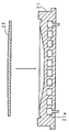
다음으로, 본 실시 형태에 따른 시료대(2)의 상세를 설명한다. 도 2는, 본 실시 형태에 따른 시료대(2)의 일 예를 개략적으로 나타내는 측단면도, 도 3(a) 및 도 3(b)는, 시료대(2)의 일 예를 개략적으로 나타내는 분해 측단면도이다. 시료대(2)는, 지지 기판(21)과, 지지 기판(21)에 접착제(22)로 접착된 흡착판(23)을 구비한다.Next, the detail of the
도 4는, 지지 기판(21)의 일 예를 개략적으로 나타내는 측단면도이다. 지지 기판(21)은, 반도체 웨이퍼(W)보다도 대경(大徑)의 대략 원반 형상으로 형성된 알루미늄 부재, 스테인리스 부재, 또는 알루미늄을 함유하는 실리콘카바이드 등으로 이루어지며, 내부에는 냉각수 유로(21a)가 형성되어 있다. 냉각수 유로(21a)는, 냉각수를 통류시킴으로써, 반도체 웨이퍼(W)를 냉각하는 것이다. 지지 기판(21)의 일단면측(상면측)에는, 정면에서 보았을 때 원형의 오목면(21b)이 형성되어 있고, 오목면(21b)의 지름 방향 외측에는 환상 홈부가 형성되며, 추가로 그 외측에는 원환상의 외주부가 형성되어 있다. 지지 기판(21)의 타단면측에 있어서는, 외주면의 지름이 확장되어 있다. 오목면(21b)은, 측단면이 사다리꼴 형상의 납작한 접시 형상을 이루고, 대략 중앙부에 형성된 평면에서 보았을 때 원형 형상의 저면부(21c)와, 저면부(21c)로부터 지름 방향 외측으로 이격됨에 따라, 오목면(21b)의 깊이가 얕아지도록 형성된 테이퍼부(21d)를 갖고 있다. 오목면(21b)의 중앙부의 깊이와, 당해 중앙부로부터 이격된 테이퍼부(taperd portion; 21d)의 깊이와의 차이는, 후술하는 바와 같이 당해 중앙부에 접촉하는 부위에 있어서의 흡착판(23)의 두께와, 상기 테이퍼부(21d)에 접촉하는 부위에 있어서의 흡착판(23)의 두께와의 차이보다도 커지도록 가공되어 있다. 즉, 오목면(21b)은, 흡착판(23)을 당해 오목면(21b)에 접착한 경우, 흡착판(23)이 오목 형상이 되는 바와 같은 깊이를 갖고 있다.4 is a side cross-sectional view schematically showing an example of the
도 5는, 흡착판(23)의 일 예를 개략적으로 나타내는 주요부를 확대한 측단면도이다. 흡착판(23)은, 지지 기판(21)의 오목면(21b)과 대략 동일 또는 대경의 원반 형상을 이루는 세라믹 부재로 구성되어 있다. 흡착판(23)은, 반도체 웨이퍼(W)에 접촉하여 흡착하는 접촉면(23c)과, 당해 접촉면(23c)의 반대측의 면인 비접촉면(23b)를 갖는 판 부재(23a)를 구비한다. 접촉면(23c)은, 엠보싱 가공이 행해진 후, 랩핑 가공으로 엠보싱 두정부(頭頂部)가 평활화되어 있다. 랩핑 가공이 행해진 흡착판(23)은, 대략 중앙부가 외주 부분에 비해 볼록 형상으로 만곡되어 있다. 비접촉면(23b)은, 도 2에 나타내는 바와 같이, 지지 기판(21)의 오목면(21b)에 접착제(22)로 접착되어 있다. 지지 기판(21)의 오목면(21b)은, 측단면이 사다리꼴 형상이지만, 오목면(21b)과 흡착판(23)과의 간극에 접착제(22)가 침윤(permeation)되어 있어, 흡착판(23)의 접촉면(23c)은, 매끄럽게 만곡된 오목 형상이 된다. 또한, 흡착판(23)은, 반도체 웨이퍼(W)를 과열하기 위한 히터(23e)와, 반도체 웨이퍼(W)를 정전 흡착하기 위한 전극(23d)이 매설되어 있고, 히터(23e) 및 전극(23d)에는, 각각 히터 전원(6) 및 DC 전원(8)이 접속되어 있다. 5 is an enlarged side cross-sectional view of a main part schematically showing an example of the
또한, 도 2∼도 5에 나타낸 오목면(21b), 흡착판(23)의 오목 형상은, 과장되게 그려진 것으로, 지지 기판(21)에 접착된 흡착판(23)의 접촉면(23c)은, 한없이 평탄에 가까운 오목 형상이다.In addition, the concave shape of the recessed
도 6은, 지지 기판(21)의 치수를 설명하기 위한 설명도이다. 지지 기판(21)의 일단면측에서 오목면(21b)이 형성된 원형 부분의 직경(φ)은, 예를 들면 300mm, 오목면(21b)의 저면부(21c)의 직경(φχ)은 150mm, 오목면(21b)의 중앙부에 있어서의 깊이(D)는, 약 20∼25㎛, 저면부(21c)와, 테이퍼부(21d)가 이루는 각도(θ)는, 179.981°∼179.985°이다. 또한, 직경(φ, φχ), 깊이(D), 각도(θ)의 값은 일 예이며, 반도체 웨이퍼(W) 및 흡착판(23)의 치수 및 두께에 따라서 적절히 설정하면 좋다. 단, φ가 300mm이고 깊이(D)=약 20∼25㎛인 오목면(21b)을 절삭 가공하는 경우, 저면부(21c)의 직경(φχ)을 150mm로 설정하면, 예를 들면 직경(φχ)을 100mm로 설정하는 경우에 비해, 정밀도 좋게 가공할 수 있는 것이 확인되어 있다.6 is an explanatory diagram for explaining the dimensions of the
도 7은, 지지 기판(21)에 형성된 오목면(21b)의 치수 형상을 설명하기 위한 그래프이다. 횡축은 직경(φχ), 종축은 각도(θ)이다. 굵은 선으로 나타낸 그래프는, φ가 300mm이고 깊이(D)=약 20∼25㎛인 오목부를 실현하기 위한 각도(θ)의 상한값을 나타내고, 가는 선은 θ의 하한값을 나타내고 있다. 기준값은, φχ가 150mm일 때의 θ의 하한값이다.7 is a graph for explaining the dimensional shape of the
도 8은, 지지 기판(21)에 형성된 오목면(21b)의 깊이를 나타낸 그래프이다. 횡축은, 오목면(21b)의 지름 방향 위치, 종축은 깊이(D)를 나타내고 있다. 사각표 및 마름모꼴표의 플롯은, 각각 따로 절삭 가공된 오목면(21b)의 깊이를 나타내고 있어, 오목면(21b)이 재현성 좋게 형성되어 있는 것이 확인되었다.8 is a graph showing the depth of the
도 9는, 본 실시 형태에 따른 시료대(2)의 작용을 설명하기 위한 설명도이다. 도 9(a)는, 도 10과 동일하게, 반도체 웨이퍼(W)가 올려놓여진 시료대(2)를 개략적으로 나타내고 있다. 도 9(b)는, 플라즈마 환경하에 있어서, 시료대(2)에 올려놓여진 반도체 웨이퍼(W)에 있어서의 온도 분포의 측정 결과를 나타내고 있다. 본 실시 형태에서는, 흡착판(23)의 접촉면(23c)을 평활하게 하기 위해 랩핑 가공을 행한 경우라도, 지지 기판(21)에 오목면(21b)이 형성되고, 오목면(21b)에 흡착판(23)이 접착되어 있기 때문에, 접촉면(23c)은 도 9(a)에 나타내는 바와 같이, 대략 중앙부가 평탄 내지 오목 형상으로 만곡된 형상이 된다. 또한, 도 9(a)에 나타낸 오목 형상은, 과장되게 그려진 것으로, 실제는 한없이 평탄에 가까운 오목 형상이다. 이와 같이, 흡착판(23) 상에 대하여 수평으로 올려놓여진 반도체 웨이퍼(W)는 안정적으로 선 지지되고, 그 결과, 도 9(b)에 나타내는 바와 같이, 반도체 웨이퍼(W)의 열저항은 균일하게 되어, 반도체 웨이퍼(W)의 온도 분포는 균일해진다. 종래 기술과 동일한 실험을 본 실시 형태에 따른 시료대(2)를 이용하여 행한 결과, 반도체 웨이퍼(W)에 있어서의 국소적 온도차(ΔT)를 약 5℃로 억제할 수 있었다.9 is an explanatory diagram for explaining the operation of the
이와 같이 구성된 마이크로파 플라즈마 처리 장치 및 시료대(2)에 있어서는, 랩핑 가공에 의해 접촉면(23c)의 평활성을 유지하고, 그리고 접촉면(23c)을 대략 오목 형상으로 함으로써, 반도체 웨이퍼(W)를 안정적으로 보유지지할 수 있다.In the microwave plasma processing apparatus and the sample table 2 configured as described above, the semiconductor wafer W is stably maintained by maintaining the smoothness of the contact surface 23c by lapping and making the contact surface 23c substantially concave. Can be retained.
또한, 지지 기판(21)의 오목면(21b)을, 측단면 사다리꼴 형상으로 형성하고 있기 때문에, 오목면(21b)이 유발 형상으로 형성된 오목면(21b)에 비해, 흡착판(23)을 지지 기판(21)에 안정적으로 접착시킬 수 있다. 오목면(21b)을 유발 형상으로 형성하면, 흡착판(23)의 중앙 부분이 들떠, 흡착판(23)이 박리될 우려가 있지만, 측단면 사다리꼴 형상으로 형성한 경우, 흡착판(23)의 박리를 효과적으로 억지할 수 있다.In addition, since the
또한, 지지 기판(21)의 오목면(21b)은 측단면 사다리꼴 형상이기 때문에, 원호 형상으로 가공하는 경우에 비해, 오목면(21b)의 깊이를 고정밀도로 용이하게 가공하는 것이 가능하다. 그 결과, 흡착판(23)의 오목 형상도 고정밀도로 형성할 수 있다.In addition, since the
추가로 또한, 흡착판(23)에 매설된 전극(23d)에 직류 전류를 통류시킴으로써, 반도체 웨이퍼(W)를 흡착판(23)의 접촉면(23c)에 면접촉시킬 수 있다. 그리고, 흡착판(23)에 반도체 웨이퍼(W)가 균일하게 면접촉한 상태로, 히터(23e)에 통전시킴으로써, 반도체 웨이퍼(W)를 과열하고, 지지 기판(21)의 냉각수 유로(21a)에 냉각수를 통류시킴으로써, 반도체 웨이퍼(W)를 냉각할 수 있다. 따라서, 반도체 웨이퍼(W)의 온도를 균일하게 제어하여, 반도체 웨이퍼(W)를 균일하게 플라즈마 처리할 수 있다.In addition, the semiconductor wafer W can be brought into surface contact with the contact surface 23c of the
또한, 실시 형태에서 나타낸 오목면의 형상은, 일 예이며, 그 형상은 한정되는 것은 아니다. 예를 들면, 가공 정밀도를 담보할 수 있으면, 오목면을 원호 형상으로 형성해도 좋다. 또한, 흡착판을 지지 기판에 접착하는 것이 가능하면, 오목면을 유발 형상으로 형성해도 좋다.In addition, the shape of the concave surface shown in embodiment is an example, The shape is not limited. For example, as long as processing accuracy can be ensured, the concave surface may be formed in an arc shape. In addition, as long as it is possible to adhere the adsorption plate to the support substrate, the concave surface may be formed in a triggered shape.
또한, 본 실시 형태에 따른 시료대가 적용되는 반도체 제조 장치는 특별히 한정되는 것은 아니고, PVD, CVD, 플라즈마 CVD 등의 성막 처리 장치, 에칭 장치 등, 각종 처리 장치에 적용할 수 있다.In addition, the semiconductor manufacturing apparatus to which the sample stand which concerns on this embodiment is applied is not specifically limited, It is applicable to various processing apparatuses, such as film-forming apparatuses, such as PVD, CVD, and plasma CVD, an etching apparatus.
이번에 개시된 실시 형태는 모든 점에서 예시로서, 제한적인 것은 아니라고 생각되어야 할 것이다. 본 발명의 범위는, 상기한 의미가 아니라, 청구의 범위에 의해 나타나고, 청구의 범위와 균등한 의미 및 범위 내에서의 모든 변경이 포함되는 것이 의도된다.Embodiment disclosed this time is an illustration in all the points, Comprising: It should be thought that it is not restrictive. The scope of the present invention is shown not by the above-mentioned meaning but by the Claim, and it is intended that the meaning of a claim and equality and all the changes within a range are included.
1 : 처리실
2 : 시료대
6 : 히터 전원
8 : DC 전원
21 : 지지 기판
21a : 냉각수 유로
21b : 오목면
21c : 저면부
21d : 테이퍼부
22 : 접착제
23 : 흡착판
23a : 판 부재
23b : 비접촉면
23c : 접촉면
23d : 전극
23e : 히터
W : 반도체 웨이퍼1: Treatment room
2:
6: heater power
8: DC power
21: support substrate
21a: coolant flow path
21b: concave
21c: bottom part
21d: taper
22: Adhesive
23: adsorption plate
23a: plate member
23b: non-contact surface
23c: contact surface
23d: electrode
23e: heater
W: Semiconductor wafer
Claims (5)
피처리 기판이 접촉하는 접촉면을 갖고, 당해 접촉면에 접촉한 피처리 기판을 흡착하는 흡착판과,
당해 흡착판의 비접촉면이 접착된 오목면을 갖는 지지 기판을 구비하고,
상기 오목면의 중앙부의 깊이(D)는, 상기 지지 기판의 일단면측에서 상기 오목면이 형성된 원형부분의 직경(φ)에 대하여 6.66×10⁻⁵~8.33×10⁻⁵배의 범위로 설정되고,
상기 오목면의 중앙부의 깊이와, 당해 중앙부로부터 이격된 이격 부위의 깊이와의 차이는, 당해 중앙부에 접촉하는 부위에 있어서의 상기 흡착판의 두께와, 상기 이격 부위에 접촉하는 부위에 있어서의 상기 흡착판의 두께와의 차이보다도 큰 것을 특징으로 하는 시료대.A sample stage for holding a to-be-processed substrate on which substrate processing is to be performed,
An adsorption plate having a contact surface to which the substrate to be treated contacts, and adsorbing the substrate to be contacted with the contact surface;
A support substrate having a concave surface to which a non-contact surface of the suction plate is bonded,
The depth D of the central portion of the concave surface is set in a range of 6.66 × 10 −5 to 8.33 × 10 −5 times the diameter φ of the circular portion where the concave surface is formed at one end side of the support substrate. ,
The difference between the depth of the center portion of the concave surface and the depth of the separation portion spaced from the center portion is the thickness of the suction plate in the portion in contact with the center portion and the suction plate in the portion in contact with the separation portion. A sample stand characterized in that it is larger than the difference from the thickness.
상기 지지 기판의 오목면은, 평탄한 저면부를 갖는 것을 특징으로 하는 시료대.The method of claim 1,
A concave surface of the support substrate has a flat bottom surface portion.
상기 지지 기판의 오목면은, 측단면이 사다리꼴 형상인 것을 특징으로 하는 시료대.3. The method according to claim 1 or 2,
The concave surface of the said support substrate is a sample stand characterized by the side cross section of a trapezoid shape.
상기 지지 기판은,
알루미늄 부재로 이루어지며, 피처리 기판을 냉각하기 위한 냉각수가 통류하는 냉각수 유로를 구비하고,
상기 흡착판은,
상기 접촉면에 랩핑(lapping) 가공이 행해진 세라믹 부재로 이루어지며, 피처리 기판을 가열하기 위한 히터와, 피처리 기판을 정전 흡착하기 위한 전극을 당해 세라믹 부재의 내부에 구비하는 것을 특징으로 하는 시료대.3. The method according to claim 1 or 2,
Wherein the support substrate comprises:
An aluminum member, provided with a cooling water flow path through which cooling water flows for cooling the substrate to be processed,
The adsorption plate,
And a heater for heating the substrate and an electrode for electrostatic adsorption of the substrate to be processed. The sample table includes a ceramic member having a lapping process on the contact surface. .
Applications Claiming Priority (3)
| Application Number | Priority Date | Filing Date | Title |
|---|---|---|---|
| JPJP-P-2009-241538 | 2009-10-20 | ||
| JP2009241538A JP5628507B2 (en) | 2009-10-20 | 2009-10-20 | Sample stage and microwave plasma processing equipment |
| PCT/JP2010/066910 WO2011048917A1 (en) | 2009-10-20 | 2010-09-29 | Sample table and microwave plasma processing apparatus |
Publications (2)
| Publication Number | Publication Date |
|---|---|
| KR20120060889A KR20120060889A (en) | 2012-06-12 |
| KR101324589B1 true KR101324589B1 (en) | 2013-11-01 |
Family
ID=43900155
Family Applications (1)
| Application Number | Title | Priority Date | Filing Date |
|---|---|---|---|
| KR1020127010099A KR101324589B1 (en) | 2009-10-20 | 2010-09-29 | Sample table and microwave plasma processing apparatus |
Country Status (6)
| Country | Link |
|---|---|
| US (1) | US20120211165A1 (en) |
| JP (1) | JP5628507B2 (en) |
| KR (1) | KR101324589B1 (en) |
| CN (1) | CN102576673B (en) |
| TW (1) | TWI459502B (en) |
| WO (1) | WO2011048917A1 (en) |
Families Citing this family (5)
| Publication number | Priority date | Publication date | Assignee | Title |
|---|---|---|---|---|
| WO2014024216A1 (en) * | 2012-08-06 | 2014-02-13 | パイオニア株式会社 | Dry etching device and dry etching method |
| JP6741548B2 (en) * | 2016-10-14 | 2020-08-19 | 日本碍子株式会社 | Member for semiconductor manufacturing apparatus and manufacturing method thereof |
| US10510512B2 (en) * | 2018-01-25 | 2019-12-17 | Tokyo Electron Limited | Methods and systems for controlling plasma performance |
| CN110983298A (en) * | 2019-12-24 | 2020-04-10 | 中国科学院半导体研究所 | Sample table structure for microwave plasma chemical vapor deposition device |
| KR20220086013A (en) | 2020-12-16 | 2022-06-23 | 삼성전자주식회사 | Semiconductor processing equipment including electrostatic chuck for plasma processing |
Citations (3)
| Publication number | Priority date | Publication date | Assignee | Title |
|---|---|---|---|---|
| JP2004273619A (en) * | 2003-03-06 | 2004-09-30 | Hitachi High-Technologies Corp | Test piece setting device for vacuum processing apparatus |
| JP2006013302A (en) * | 2004-06-29 | 2006-01-12 | Ngk Insulators Ltd | Substrate mounting device and substrate temperature adjusting method |
| JP2009510774A (en) * | 2005-09-30 | 2009-03-12 | ラム リサーチ コーポレーション | Electrostatic chuck assembly comprising a dielectric material and / or cavity having varying thickness, profile and / or shape, method of use thereof, and apparatus incorporating the same |
Family Cites Families (12)
| Publication number | Priority date | Publication date | Assignee | Title |
|---|---|---|---|---|
| US5886863A (en) * | 1995-05-09 | 1999-03-23 | Kyocera Corporation | Wafer support member |
| US5761023A (en) * | 1996-04-25 | 1998-06-02 | Applied Materials, Inc. | Substrate support with pressure zones having reduced contact area and temperature feedback |
| US6177023B1 (en) * | 1997-07-11 | 2001-01-23 | Applied Komatsu Technology, Inc. | Method and apparatus for electrostatically maintaining substrate flatness |
| US6228438B1 (en) * | 1999-08-10 | 2001-05-08 | Unakis Balzers Aktiengesellschaft | Plasma reactor for the treatment of large size substrates |
| JP3650025B2 (en) * | 2000-12-04 | 2005-05-18 | シャープ株式会社 | Plasma process equipment |
| GB0029570D0 (en) * | 2000-12-05 | 2001-01-17 | Trikon Holdings Ltd | Electrostatic clamp |
| US7651571B2 (en) * | 2005-12-22 | 2010-01-26 | Kyocera Corporation | Susceptor |
| US8284538B2 (en) * | 2006-08-10 | 2012-10-09 | Tokyo Electron Limited | Electrostatic chuck device |
| US20080041312A1 (en) * | 2006-08-10 | 2008-02-21 | Shoichiro Matsuyama | Stage for plasma processing apparatus, and plasma processing apparatus |
| US7619870B2 (en) * | 2006-08-10 | 2009-11-17 | Tokyo Electron Limited | Electrostatic chuck |
| JP4943085B2 (en) * | 2006-08-10 | 2012-05-30 | 東京エレクトロン株式会社 | Electrostatic chuck apparatus and plasma processing apparatus |
| JP5029089B2 (en) * | 2007-03-26 | 2012-09-19 | 東京エレクトロン株式会社 | Mounting table for plasma processing apparatus and plasma processing apparatus |
-
2009
- 2009-10-20 JP JP2009241538A patent/JP5628507B2/en active Active
-
2010
- 2010-09-29 CN CN201080047610.7A patent/CN102576673B/en active Active
- 2010-09-29 US US13/502,829 patent/US20120211165A1/en not_active Abandoned
- 2010-09-29 KR KR1020127010099A patent/KR101324589B1/en active IP Right Grant
- 2010-09-29 WO PCT/JP2010/066910 patent/WO2011048917A1/en active Application Filing
- 2010-10-19 TW TW099135496A patent/TWI459502B/en active
Patent Citations (3)
| Publication number | Priority date | Publication date | Assignee | Title |
|---|---|---|---|---|
| JP2004273619A (en) * | 2003-03-06 | 2004-09-30 | Hitachi High-Technologies Corp | Test piece setting device for vacuum processing apparatus |
| JP2006013302A (en) * | 2004-06-29 | 2006-01-12 | Ngk Insulators Ltd | Substrate mounting device and substrate temperature adjusting method |
| JP2009510774A (en) * | 2005-09-30 | 2009-03-12 | ラム リサーチ コーポレーション | Electrostatic chuck assembly comprising a dielectric material and / or cavity having varying thickness, profile and / or shape, method of use thereof, and apparatus incorporating the same |
Also Published As
| Publication number | Publication date |
|---|---|
| US20120211165A1 (en) | 2012-08-23 |
| TW201133699A (en) | 2011-10-01 |
| KR20120060889A (en) | 2012-06-12 |
| WO2011048917A1 (en) | 2011-04-28 |
| TWI459502B (en) | 2014-11-01 |
| CN102576673A (en) | 2012-07-11 |
| JP2011091096A (en) | 2011-05-06 |
| JP5628507B2 (en) | 2014-11-19 |
| CN102576673B (en) | 2015-08-19 |
Similar Documents
| Publication | Publication Date | Title |
|---|---|---|
| KR102383357B1 (en) | Mounting table and substrate processing apparatus | |
| TWI763969B (en) | Tapered upper electrode for uniformity control in plasma processing | |
| US9595425B2 (en) | Antenna, dielectric window, plasma processing apparatus and plasma processing method | |
| KR102434559B1 (en) | Mounting table and plasma processing apparatus | |
| KR101265807B1 (en) | Heat transfer system for improved semiconductor processing uniformity | |
| USRE40046E1 (en) | Processing system | |
| US20100006543A1 (en) | Plasma processing apparatus, plasma processing method and storage medium | |
| KR101324589B1 (en) | Sample table and microwave plasma processing apparatus | |
| KR20180076311A (en) | Focus ring and substrate processing apparatus | |
| US20170301578A1 (en) | Focus ring assembly and a method of processing a substrate using the same | |
| CN108242381B (en) | Gas supply device, method for manufacturing the same, and plasma processing apparatus | |
| JP2014007215A (en) | Processing unit of workpiece and mounting table of workpiece | |
| JP2019176030A (en) | Plasma processing apparatus | |
| TW201436034A (en) | Substrate support for plasma etch operations | |
| KR101898079B1 (en) | Plasma processing apparatus | |
| JP2017126727A (en) | Structure of mounting table and semiconductor processing device | |
| US11398397B2 (en) | Electrostatic chuck and plasma processing apparatus including the same | |
| US20080025899A1 (en) | Plasma surface treatment method, quartz member, plasma processing apparatus and plasma processing method | |
| US10896842B2 (en) | Manufacturing method of sample table | |
| TWI757671B (en) | Heated pedestal design for improved heat transfer and temperature uniformity | |
| KR102650167B1 (en) | electrostatic chuck and plasma processing apparatus including the same | |
| JP2010010231A (en) | Plasma treatment device | |
| JP2010021405A (en) | Plasma processing apparatus | |
| JP5927260B2 (en) | Sample stage and microwave plasma processing equipment | |
| JP3881290B2 (en) | Plasma processing equipment |
Legal Events
| Date | Code | Title | Description |
|---|---|---|---|
| A201 | Request for examination | ||
| E902 | Notification of reason for refusal | ||
| E701 | Decision to grant or registration of patent right | ||
| GRNT | Written decision to grant |