WO2011039799A1 - センサアレイ - Google Patents
センサアレイ Download PDFInfo
- Publication number
- WO2011039799A1 WO2011039799A1 PCT/JP2009/004979 JP2009004979W WO2011039799A1 WO 2011039799 A1 WO2011039799 A1 WO 2011039799A1 JP 2009004979 W JP2009004979 W JP 2009004979W WO 2011039799 A1 WO2011039799 A1 WO 2011039799A1
- Authority
- WO
- WIPO (PCT)
- Prior art keywords
- membrane
- sensor
- sensor array
- frame
- shape
- Prior art date
- Legal status (The legal status is an assumption and is not a legal conclusion. Google has not performed a legal analysis and makes no representation as to the accuracy of the status listed.)
- Ceased
Links
Images



Classifications
-
- G—PHYSICS
- G01—MEASURING; TESTING
- G01J—MEASUREMENT OF INTENSITY, VELOCITY, SPECTRAL CONTENT, POLARISATION, PHASE OR PULSE CHARACTERISTICS OF INFRARED, VISIBLE OR ULTRAVIOLET LIGHT; COLORIMETRY; RADIATION PYROMETRY
- G01J5/00—Radiation pyrometry, e.g. infrared or optical thermometry
- G01J5/10—Radiation pyrometry, e.g. infrared or optical thermometry using electric radiation detectors
- G01J5/34—Radiation pyrometry, e.g. infrared or optical thermometry using electric radiation detectors using capacitors, e.g. pyroelectric capacitors
-
- B—PERFORMING OPERATIONS; TRANSPORTING
- B81—MICROSTRUCTURAL TECHNOLOGY
- B81B—MICROSTRUCTURAL DEVICES OR SYSTEMS, e.g. MICROMECHANICAL DEVICES
- B81B3/00—Devices comprising flexible or deformable elements, e.g. comprising elastic tongues or membranes
- B81B3/0064—Constitution or structural means for improving or controlling the physical properties of a device
- B81B3/0067—Mechanical properties
- B81B3/007—For controlling stiffness, e.g. ribs
-
- G—PHYSICS
- G01—MEASURING; TESTING
- G01J—MEASUREMENT OF INTENSITY, VELOCITY, SPECTRAL CONTENT, POLARISATION, PHASE OR PULSE CHARACTERISTICS OF INFRARED, VISIBLE OR ULTRAVIOLET LIGHT; COLORIMETRY; RADIATION PYROMETRY
- G01J5/00—Radiation pyrometry, e.g. infrared or optical thermometry
- G01J5/02—Constructional details
- G01J5/0225—Shape of the cavity itself or of elements contained in or suspended over the cavity
- G01J5/024—Special manufacturing steps or sacrificial layers or layer structures
-
- H—ELECTRICITY
- H10—SEMICONDUCTOR DEVICES; ELECTRIC SOLID-STATE DEVICES NOT OTHERWISE PROVIDED FOR
- H10F—INORGANIC SEMICONDUCTOR DEVICES SENSITIVE TO INFRARED RADIATION, LIGHT, ELECTROMAGNETIC RADIATION OF SHORTER WAVELENGTH OR CORPUSCULAR RADIATION
- H10F39/00—Integrated devices, or assemblies of multiple devices, comprising at least one element covered by group H10F30/00, e.g. radiation detectors comprising photodiode arrays
- H10F39/10—Integrated devices
- H10F39/12—Image sensors
- H10F39/191—Photoconductor image sensors
- H10F39/193—Infrared image sensors
-
- H—ELECTRICITY
- H10—SEMICONDUCTOR DEVICES; ELECTRIC SOLID-STATE DEVICES NOT OTHERWISE PROVIDED FOR
- H10F—INORGANIC SEMICONDUCTOR DEVICES SENSITIVE TO INFRARED RADIATION, LIGHT, ELECTROMAGNETIC RADIATION OF SHORTER WAVELENGTH OR CORPUSCULAR RADIATION
- H10F39/00—Integrated devices, or assemblies of multiple devices, comprising at least one element covered by group H10F30/00, e.g. radiation detectors comprising photodiode arrays
- H10F39/80—Constructional details of image sensors
- H10F39/802—Geometry or disposition of elements in pixels, e.g. address-lines or gate electrodes
-
- B—PERFORMING OPERATIONS; TRANSPORTING
- B81—MICROSTRUCTURAL TECHNOLOGY
- B81B—MICROSTRUCTURAL DEVICES OR SYSTEMS, e.g. MICROMECHANICAL DEVICES
- B81B2201/00—Specific applications of microelectromechanical systems
- B81B2201/02—Sensors
- B81B2201/0264—Pressure sensors
-
- B—PERFORMING OPERATIONS; TRANSPORTING
- B81—MICROSTRUCTURAL TECHNOLOGY
- B81B—MICROSTRUCTURAL DEVICES OR SYSTEMS, e.g. MICROMECHANICAL DEVICES
- B81B2201/00—Specific applications of microelectromechanical systems
- B81B2201/02—Sensors
- B81B2201/0278—Temperature sensors
-
- B—PERFORMING OPERATIONS; TRANSPORTING
- B81—MICROSTRUCTURAL TECHNOLOGY
- B81B—MICROSTRUCTURAL DEVICES OR SYSTEMS, e.g. MICROMECHANICAL DEVICES
- B81B2203/00—Basic microelectromechanical structures
- B81B2203/01—Suspended structures, i.e. structures allowing a movement
- B81B2203/0127—Diaphragms, i.e. structures separating two media that can control the passage from one medium to another; Membranes, i.e. diaphragms with filtering function
-
- B—PERFORMING OPERATIONS; TRANSPORTING
- B81—MICROSTRUCTURAL TECHNOLOGY
- B81B—MICROSTRUCTURAL DEVICES OR SYSTEMS, e.g. MICROMECHANICAL DEVICES
- B81B2207/00—Microstructural systems or auxiliary parts thereof
- B81B2207/05—Arrays
- B81B2207/053—Arrays of movable structures
Definitions
- the present invention relates to a sensor array in which sensor elements having a membrane structure sensitive to temperature change, pressure change, vibration, and the like are connected in a planar shape.
- thermosensor element having a membrane structure
- This thermal sensor includes a square membrane composed of a thermal sensitivity element and upper and lower electrodes, and a pair of support arms that support the membrane so as to release the membrane on the substrate.
- the support arm is a wiring connected to the electrodes. It is formed with a heat insulating material.
- the thermosensitive element absorbs infrared rays, converts the temperature change into an electric signal, and enables detection.
- a large number of thermal sensors are formed in a matrix on the substrate, so that a sensor array incorporated in an infrared image sensor, a night vision device or the like is configured.
- thermosensitive element of the membrane is composed of a ferroelectric material, there is a problem that microphonic noise is generated due to vibration and detection sensitivity is lowered. Further, in the sensor array using the thermal sensor as the sensor element, there is a problem that the area ratio of the membrane (sensitive portion) to the whole is low, the size is large, and the detection sensitivity is inferior.
- a plurality of sensor elements each including a polygonal frame-like frame portion formed by connecting a plurality of frame pieces and a membrane having sensor sensitivity installed in the frame portion are adjacent to each other.
- the sensor elements are arranged in a planar shape while sharing the frame pieces in the sensor element.
- the membrane can be integrated with the frame portion, the strength of the membrane can be increased, and the rigidity (strength) of the entire sensor array can be increased. For this reason, each membrane can be formed thin while increasing the yield. Further, by integrating the membrane and the frame portion, the resonance frequency of the membrane can be extremely increased, so that destruction and breakage due to vibration can be prevented, and generation of microphonic noise can be prevented. Furthermore, since the frame pieces are shared by adjacent sensor elements, the ratio of the total area of the membrane to the total area of the frame part can be increased while increasing the rigidity (strength) of the entire sensor array, and the detection sensitivity can be increased. Can be improved.
- sharing (combining) frame pieces is a positional relationship in which, for example, adjacent sensor elements are connected (joined) to one frame piece from opposite directions in the plane.
- the frame piece has a structure in which membranes are arranged on both sides thereof, so that the strength can be increased by integrating the frame piece and the membrane.
- the width in the in-plane direction of the frame part is configured to be sufficiently smaller than the length of each sensor element, the frame part can be made into a thin frame part. Can be increased.
- each membrane has at least a peripheral portion joined to the inner peripheral surface of the frame portion in an uneven shape.
- the strength and integrity of the membrane and the frame portion are achieved, the stress concentration at the joint portion is alleviated, and the strength of the membrane itself can be increased. For this reason, the membrane can be formed thin while increasing the yield.
- the shape of the concavo-convex shape is different between two adjacent sensor elements.
- two adjacent sensor elements can be set to different resonance frequencies, and the resonance frequency can be kept low for the entire sensor array. Therefore, destruction / breakage due to vibration can be prevented, and a sensor array suitable for in-vehicle use can be configured.
- each concavo-convex shape extends in at least two directions, and that the concave portions and the convex portions are distributed in a mesh shape in the entire in-plane area of each membrane.
- the strength of the membrane itself can be further increased, and the membrane can be formed thin accordingly. Further, the strength of the entire sensor array can be increased.
- the polygon is any one of a triangle, a square, and a hexagon.
- Each membrane is preferably formed by laminating a front electrode layer, a dielectric layer, and a back electrode layer.
- a sensor element having a high yield and high detection sensitivity can be configured.
- the ratio of the total area of the membrane to the total area of the frame portion is increased while increasing the rigidity (strength) of the entire sensor array.
- the detection sensitivity can be improved. That is, it can be formed compactly, and the yield and detection sensitivity can be improved.
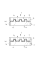
- FIG. 2 is a cross-sectional view taken along line AA in FIG. 1 and a cross-sectional view taken along line BB (b).
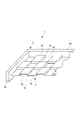
- FIG. 2 is a fragmentary perspective view of the infrared sensor which concerns on 1st Embodiment.
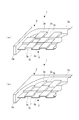
- It is a fragmentary perspective view of the infrared sensor explaining the modification (a) around a frame part, and another modification (b).
- It is sectional drawing of the infrared sensor explaining the modification (a) around a membrane, and another modification (b). It is explanatory drawing which shows the manufacturing method of the infrared sensor which concerns on 1st Embodiment.
- an infrared sensor which is a MEMS sensor according to an embodiment of the present invention and a sensor array using the same will be described with reference to the accompanying drawings.
- This infrared sensor is manufactured by microfabrication technology using silicon (wafer) or the like as a material, and is constituted by a so-called pyroelectric infrared (far infrared) sensor. Further, this infrared sensor constitutes a pixel (element) of a sensor array (infrared detector) that is commercialized in an array format.
- the infrared sensor 1 includes a frame portion 2 formed in a rectangular frame shape, and a membrane 3 that is installed in the frame portion 2 and formed in an uneven shape as a whole. ing.
- the membrane 3 is a so-called infrared detection unit having sensor sensitivity, and is formed as thin as possible.
- the frame portion 2 is a portion that supports the thinly formed membrane 3 over four circumferences, and although not shown in the drawing, a connection wiring to the membrane 3 is patterned on the surface thereof.
- the frame part 2 is formed in a square frame shape by deep reactive etching (Deep RIE) from both sides of the silicon substrate. Further, the four frame pieces 2a constituting each side of the frame portion 2 have the same thickness.
- the frame part 2 of the embodiment is formed with a size of about 50 ⁇ m on one side, for example.
- the frame portion 2 is preferably formed in a polygonal shape in consideration of strength, such as a rectangle, a triangle, and a hexagon, in addition to a square.
- the frame portion 2 in FIG. 4 (a) has each corner portion formed in a small round shape (large curvature radius), and the frame portion 2 in FIG. 4 (b) has a large round shape (curvature) in each corner portion. (Small radius).
- the rigidity of the frame portion 2 can be increased in the planar direction, and as a result, the strength of the entire infrared sensor 1 can be increased.
- the membrane 3 is configured by laminating an upper electrode layer 11, a pyroelectric layer (dielectric layer) 12, and a lower electrode layer 13 in this order.
- the pyroelectric layer 12 is made of, for example, PZT (Pb (Zr, Ti) O 3 ), SBT (SrBi 2 Ta 2 O 9 ), BIT (Bi 4 Ti 3 O 12 ), LT (LiTaO 3 ), LN (LiNbO 3 ). ), BTO (BaTiO 3 ), BST (BaSrTiO 3 ) and the like.
- the pyroelectric layer 12 is preferably made of a material having a high dielectric constant in consideration of detection sensitivity (for example, BST (BaSrTiO 3 ) or LT (LiTaO 3 )).
- the pyroelectric layer 12 of the embodiment is formed to a thickness of about 0.2 ⁇ m.
- the lower electrode layer 13 is made of, for example, Au, SRO, Nb-STO, LNO (LaNiO 3 ), or the like.
- the lower electrode layer 13 is preferably made of the same material as that of the pyroelectric layer 12.
- the lower electrode layer 13 may be made of general Pt, Ir, Ti or the like.
- the upper electrode layer 11 is made of, for example, Au-Black or the like so as to increase the infrared absorption rate.
- the upper electrode layer 11 and the lower electrode layer 13 of the embodiment are each formed to a thickness of about 0.1 ⁇ m.
- the membrane 3 having such a laminated structure is formed in a concavo-convex shape in a plane, in other words, in a two-dimensional concavo-convex shape.
- the concave-convex shape extends in two directions orthogonal to each other, and the concave portions 3a and the convex portions 3b having a square shape in plan view are distributed in a mesh shape (matrix shape) in the entire in-plane region of the membrane 3. Yes. That is, four convex portions 3b are adjacent to any one concave portion 3a, and four concave portions 3a are adjacent to any one convex portion 3b. For this reason, as shown in FIG. 2A, FIG. 2B, and FIG.
- the joining portion with respect to each frame piece 2a is also uneven in a plan view.
- the planar shapes of the recesses 3a and the projections 3b are preferably rectangles, triangles, etc., or polygons such as rectangles, triangles, etc. with rounded corners. And convex parts may be mixed.
- the adjacent concave portion 3a and convex portion 3b also serve as a peripheral wall 3c, and this peripheral wall 3c constitutes a part of the infrared detector and functions as a reinforcing rib.
- the height of the peripheral wall 3c functioning as a reinforcing rib is formed larger than the thickness dimension of the membrane 3.
- the separation dimension in the front and back direction is formed to be about 2.5 ⁇ m.
- the reinforcing rib of the embodiment is formed at right angles to the in-plane direction of the membrane 3, it may be inclined. That is, as shown in FIG. 5A, the uneven shape of the membrane 3 is a cross-sectional shape in which inverted trapezoidal concave portions 3a and trapezoidal convex portions 3b are alternately connected. At that time, as shown in FIG. 5 (b), it is more preferable to round the corners and corners of the recess 3a and the protrusion 3b (to form a round shape). Further, the same roundness is applied to the embodiment of FIG. Thereby, the rigidity of the membrane 3 can be increased in the front and back directions, and the strength of the entire infrared sensor 1 can be increased together with the frame portion 2.
- the infrared sensor 1 of the embodiment uses a silicon substrate (wafer) W and is manufactured by a semiconductor microfabrication technique.
- a first etching deep reactive etching: anisotropic etching
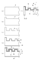
- a resist is applied by photolithography, so that the convex portion 3b. Is formed (actually, the portion corresponding to the back surface of the lower electrode layer 13 in the convex portion 3b) (FIG. 6B).
- the second etching deep reactive etching: anisotropic etching
- the second etching is performed from the upper side (front side) to form a plurality of concave portions 3a (actually concave portions on the back surface of the lower electrode layer 13). Part) is formed (FIG. 6C).
- a thermal oxidation process is performed to form oxide films (SiO 2 ) Wa on the front and back surfaces of the silicon substrate W (FIG. 6D).
- the lower electrode layer 13, the pyroelectric layer 12, and the upper electrode layer 11 are formed in this order, for example, by epitaxial growth (CVD), which later becomes the membrane 3 Is deposited (FIG. 6E).
- CVD epitaxial growth
- the buffer layer for example YSZ, CeO 2, Al 2 O 3, STO is preferred.
- third etching (for example, isotropic etching by wet etching) is performed from the front side from the back side or the silicon substrate W is turned upside down, and the substrate portion under the membrane 3 is removed.
- the lower electrode layer 13 of the membrane 3 is caused to function as an etching stop layer, while the frame portion 2 is left by managing the etching time.
- the substrate portion on the lower side of the membrane 3 may be formed as a sacrificial layer such as phosphate glass, and the sacrificial layer may be removed from the front side. Further, the oxide film Wa may not be completely removed.
- the infrared sensor 1 according to the modification of FIG. 7 includes a frame portion 2 formed in a quadrangular frame shape, and a membrane 3 that is installed in the frame portion 2 and formed in an uneven shape. It is equipped with.
- the membrane 3 of the first modified example extends so that the concavo-convex shape obliquely intersects, and the concave portions 3a and the convex portions 3b having a triangular shape in plan view are distributed in a mesh shape throughout the entire surface of the membrane. ing.
- the peripheral wall 3c serving as a reinforcing rib extends in three directions, the strength of the membrane 3 can be further increased.
- a sensor array (infrared detector) 20 having the infrared sensor 1 of the first embodiment as a sensor element will be described with reference to FIGS.
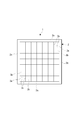
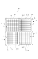
- the sensor array 20 shown in FIG. 8 has a concave portion 3a and a convex portion 3b formed in a rectangular shape in plan view in each infrared sensor 1, and a plurality of infrared sensors (sensor elements) 1 are arranged in a plane without gaps. ,It is configured.
- the plurality of infrared sensors 1 are arranged in a state in which the mutual frame portions 2 are shared, that is, in any two adjacent infrared sensors 1 in a state in which the mutual frame pieces 2a are shared. .
- any two adjacent infrared sensors 1 the shape of the uneven shape of the membrane 3 is different. That is, in one membrane 3, rectangular concave portions 3a and convex portions 3b are arranged in a so-called lateral direction, and in the other membrane 3, rectangular concave portions 3a and convex portions 3b are arranged in a so-called vertical direction.
- the frame pieces 2 a in the adjacent infrared sensors 1 are shared (in other words, shared), so that the rigidity (strength) of the sensor array 20 as a whole is increased and the total area of the frame portion 2 is increased.
- the ratio of the total area of the membrane 3 can be increased, and the yield and detection sensitivity can be improved.
- the adjacent infrared sensors 1 can be set to different resonance frequencies, and the resonance frequency of the entire sensor array 20 can be suppressed low. Therefore, destruction / breakage due to vibration of the sensor array 20 can be prevented, and the sensor array 20 suitable for in-vehicle use can be configured.
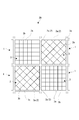
- the sensor array 20 shown in FIG. 9 has a concave portion 3a and a convex portion 3b formed in a square in plan view in each infrared sensor 1, and in this case as well, the plurality of infrared sensors 1 share the frame portion 2 with each other. In this state, they are arranged in a plane. Further, in any two adjacent infrared sensors 1, in one membrane 3, the recesses 3a and the projections 3b form a matrix in the X-axis direction and the Y-axis direction, but in the other membrane 3, the recesses 3a and The convex portion 3b is a matrix inclined by 45 ° from the X-axis direction and the Y-axis direction. Also in this case, it is possible to improve the yield and the detection sensitivity, and to prevent destruction / breakage due to vibration.
- the present invention is applied to a pressure sensor 31.
- the pressure sensor 31 includes a frame portion 32 formed in a rectangular frame shape, and a frame portion 31. And a membrane 33 partially formed in a concavo-convex shape.
- the membrane 33 in this case is configured by a capacitance detection type in which an upper electrode layer 41, a diaphragm 42, and a lower electrode layer 43 are sequentially laminated.
- the diaphragm 42 constituting the pressure receiving portion is thinly formed by etching a silicon substrate (single crystal) from both the front and back sides.
- an electrical resistance type pieoresistance
- the electrical wiring is a pn junction
- the membrane (diaphragm 42) 33 includes a central flat portion 33a that serves as a main body of the pressure receiving portion, and an uneven peripheral portion 33b that connects the central flat portion 33a and the frame portion 2. Also in this case, the peripheral edge portion 33b is formed in a two-dimensional uneven shape in the plane, and the concave portions 3a and the convex portions 3b are alternately distributed. The thickness of the membrane 3 is determined by the pressure level to be detected.
Landscapes
- Engineering & Computer Science (AREA)
- Spectroscopy & Molecular Physics (AREA)
- Physics & Mathematics (AREA)
- General Physics & Mathematics (AREA)
- Computer Hardware Design (AREA)
- Mechanical Engineering (AREA)
- Power Engineering (AREA)
- Microelectronics & Electronic Packaging (AREA)
- Manufacturing & Machinery (AREA)
- Photometry And Measurement Of Optical Pulse Characteristics (AREA)
- Measuring Fluid Pressure (AREA)
- Micromachines (AREA)
- Pressure Sensors (AREA)
- Solid State Image Pick-Up Elements (AREA)
Abstract
Description
そして、この熱センサを基板上にマトリクス状に多数形成することにより、赤外線イメージセンサやナイトビジョン装置等に組み込まれるセンサアレイが構成される。
また、熱センサをセンサエレメントとするセンサアレイでは、全体に対するメンブレン(感応部)の面積比率が低く、大型で且つ検出感度の劣るものとなる問題があった。
すなわち、フレーム片を共有(兼用)することは、例えば隣接するセンサエレメントが1つのフレーム片に対して、その面内の対向する方向からそれぞれ接続(接合)されるような位置関係であり、このような構成では、フレーム片がその両側にメンブレンを配置した構造となるので、フレーム片とメンブレンを一体としてその強度を高めることができる。また、フレーム部の面内方向における幅を各センサエレメントの長さよりも十分に小さくするように構成して、細いフレーム部とすることができるので、フレーム部の総面積に対するメンブレンの総面積の比率を高めることができる。
図7の変形例に係る赤外線センサ1は、第1実施形態と同様に、四角形の枠状に形成されたフレーム部2と、フレーム部2内に架設され、凹凸形状に形成されたメンブレン3と、を備えている。この第1変形例のメンブレン3は、凹凸形状が斜めに交差するように延在し、メンブレンの面内全域において、平面視三角形の凹部3aと凸部3bとが網目状に分布した形態となっている。この場合、補強リブとなる周壁3cが3方向に延在するため、より一層、メンブレン3の強度アップを図ることができる。
図8のセンサアレイ20は、各赤外線センサ1において、その凹部3aおよび凸部3bを平面視長方形に形成したものであり、複数の赤外線センサ(センサエレメント)1を隙間なく面状に配置して、構成されている。具体的には、複数の赤外線センサ1は、相互のフレーム部2を共有した状態で、すなわち、隣接する任意の2つの赤外線センサ1において、相互のフレーム片2aを共有した状態で配置されている。また、隣接する任意の2つの赤外線センサ1において、メンブレン3の凹凸形状の形態が異なっている。すなわち、一方のメンブレン3では、長方形の凹部3aおよび凸部3bがいわゆる横向きに配置され、他方のメンブレンで3は、長方形の凹部3aおよび凸部3bがいわゆる縦向きに配置されている。
2a フレーム片 3 メンブレン
3a 凹部 3b 凸部
11 上側電極層 12 焦電体層
13 下側電極層 20 センサアレイ
31 圧力センサ 32 フレーム部
33 メンブレン 33b 周縁部
41 上側電極層 42 ダイヤフラム
43 下側電極層 W シリコン基板
Claims (6)
- 複数のフレーム片を連設して成る多角形の枠状のフレーム部と、前記フレーム部内に架設したセンサ感度を有するメンブレンと、から成るセンサエレメントの複数個を、
隣接する前記センサエレメントにおける前記フレーム片を共有した状態で、面状に配置して成ることを特徴とするセンサアレイ。 - 前記各メンブレンは、少なくとも前記フレーム部の内周面に接合する周縁部が凹凸形状に形成されていることを特徴とする請求項1に記載のセンサアレイ。
- 隣接する2つの前記センサエレメントにおいて、前記凹凸形状の形態が相互に異なることを特徴とする請求項1に記載のセンサアレイ。
- 前記各凹凸形状は、少なくとも2方向に延在し、
前記各メンブレンの面内全域において、凹部と凸部とが網目状に分布していることを特徴とする請求項1に記載のセンサアレイ。 - 前記多角形が、三角形、四角形および六角形のいずれかであることを特徴とする請求項1に記載のセンサアレイ。
- 前記各メンブレンは、表側電極層と誘電体層と裏側電極層とを積層して成ることを特徴とする請求項1に記載のセンサアレイ。
Priority Applications (3)
| Application Number | Priority Date | Filing Date | Title |
|---|---|---|---|
| PCT/JP2009/004979 WO2011039799A1 (ja) | 2009-09-29 | 2009-09-29 | センサアレイ |
| US13/499,170 US20120230364A1 (en) | 2009-09-29 | 2009-09-29 | Sensor array |
| JP2011533947A JPWO2011039799A1 (ja) | 2009-09-29 | 2009-09-29 | センサアレイ |
Applications Claiming Priority (1)
| Application Number | Priority Date | Filing Date | Title |
|---|---|---|---|
| PCT/JP2009/004979 WO2011039799A1 (ja) | 2009-09-29 | 2009-09-29 | センサアレイ |
Publications (1)
| Publication Number | Publication Date |
|---|---|
| WO2011039799A1 true WO2011039799A1 (ja) | 2011-04-07 |
Family
ID=43825657
Family Applications (1)
| Application Number | Title | Priority Date | Filing Date |
|---|---|---|---|
| PCT/JP2009/004979 Ceased WO2011039799A1 (ja) | 2009-09-29 | 2009-09-29 | センサアレイ |
Country Status (3)
| Country | Link |
|---|---|
| US (1) | US20120230364A1 (ja) |
| JP (1) | JPWO2011039799A1 (ja) |
| WO (1) | WO2011039799A1 (ja) |
Cited By (1)
| Publication number | Priority date | Publication date | Assignee | Title |
|---|---|---|---|---|
| WO2015141496A1 (ja) * | 2014-03-19 | 2015-09-24 | 住友精密工業株式会社 | 赤外線センサ及びその製造方法 |
Families Citing this family (3)
| Publication number | Priority date | Publication date | Assignee | Title |
|---|---|---|---|---|
| FR2999805B1 (fr) * | 2012-12-17 | 2017-12-22 | Commissariat Energie Atomique | Procede de realisation d'un dispositif de detection infrarouge |
| JP7066557B2 (ja) * | 2018-07-12 | 2022-05-13 | 東京エレクトロン株式会社 | 温度測定センサ、温度測定システム、および、温度測定方法 |
| CN117990240B (zh) * | 2024-04-07 | 2024-07-02 | 华景传感科技(无锡)有限公司 | 一种微机电系统压力传感器和微机电系统压力换能器 |
Citations (5)
| Publication number | Priority date | Publication date | Assignee | Title |
|---|---|---|---|---|
| JPH01100426A (ja) * | 1987-10-14 | 1989-04-18 | Matsushita Electric Ind Co Ltd | アレイ伏焦電形赤外検出器 |
| JPH07190854A (ja) * | 1993-12-25 | 1995-07-28 | Nippondenso Co Ltd | 赤外線センサ |
| JP2001356046A (ja) * | 2000-06-13 | 2001-12-26 | Denso Corp | 赤外線検出装置 |
| JP2005268660A (ja) * | 2004-03-19 | 2005-09-29 | Horiba Ltd | 赤外線アレイセンサ |
| JP2008288813A (ja) * | 2007-05-16 | 2008-11-27 | Hitachi Ltd | 半導体装置 |
Family Cites Families (1)
| Publication number | Priority date | Publication date | Assignee | Title |
|---|---|---|---|---|
| US6410917B1 (en) * | 2000-01-18 | 2002-06-25 | The United States Of America As Represented By The Secretary Of The Army | Polarization-sensitive corrugated quantum well infrared photodetector array |
-
2009
- 2009-09-29 JP JP2011533947A patent/JPWO2011039799A1/ja not_active Abandoned
- 2009-09-29 WO PCT/JP2009/004979 patent/WO2011039799A1/ja not_active Ceased
- 2009-09-29 US US13/499,170 patent/US20120230364A1/en not_active Abandoned
Patent Citations (5)
| Publication number | Priority date | Publication date | Assignee | Title |
|---|---|---|---|---|
| JPH01100426A (ja) * | 1987-10-14 | 1989-04-18 | Matsushita Electric Ind Co Ltd | アレイ伏焦電形赤外検出器 |
| JPH07190854A (ja) * | 1993-12-25 | 1995-07-28 | Nippondenso Co Ltd | 赤外線センサ |
| JP2001356046A (ja) * | 2000-06-13 | 2001-12-26 | Denso Corp | 赤外線検出装置 |
| JP2005268660A (ja) * | 2004-03-19 | 2005-09-29 | Horiba Ltd | 赤外線アレイセンサ |
| JP2008288813A (ja) * | 2007-05-16 | 2008-11-27 | Hitachi Ltd | 半導体装置 |
Cited By (2)
| Publication number | Priority date | Publication date | Assignee | Title |
|---|---|---|---|---|
| WO2015141496A1 (ja) * | 2014-03-19 | 2015-09-24 | 住友精密工業株式会社 | 赤外線センサ及びその製造方法 |
| JPWO2015141496A1 (ja) * | 2014-03-19 | 2017-04-06 | 住友精密工業株式会社 | 赤外線センサ及びその製造方法 |
Also Published As
| Publication number | Publication date |
|---|---|
| JPWO2011039799A1 (ja) | 2013-02-21 |
| US20120230364A1 (en) | 2012-09-13 |
Similar Documents
| Publication | Publication Date | Title |
|---|---|---|
| TWI813633B (zh) | 壓電微加工超音波傳感器裝置 | |
| US8536763B2 (en) | Ultrasonic transducer, ultrasonic sensor, method of manufacturing ultrasonic transducer, and method of manufacturing ultrasonic sensor | |
| JP5936941B2 (ja) | 回転型アクチュエータ | |
| CN102564601A (zh) | 热式光检测装置、电子设备、热式光检测器及其制造方法 | |
| JP2012173191A (ja) | 熱型光検出器、熱型光検出装置及び電子機器 | |
| WO2011039799A1 (ja) | センサアレイ | |
| JP6897771B2 (ja) | コーナー結合共振子アレイ | |
| JP2009033698A (ja) | ダイアフラム構造及び音響センサ | |
| WO2011039797A1 (ja) | Memsセンサ | |
| JP2010147285A (ja) | Mems、振動ジャイロスコープおよびmemsの製造方法 | |
| JPWO2011039798A1 (ja) | Memsセンサおよびこれを備えたセンサアレイ | |
| JP2001004658A (ja) | 2軸半導体加速度センサおよびその製造方法 | |
| JP5531806B2 (ja) | 容量式慣性力センサ | |
| US7705412B2 (en) | SOI substrate and semiconductor acceleration sensor using the same | |
| CN104048764B (zh) | 背面照射型的红外传感器 | |
| WO2010073288A1 (ja) | 赤外線センサおよび赤外線センサの製造方法 | |
| JP6186364B2 (ja) | ミラーデバイスの製造方法 | |
| JP2010243420A (ja) | Memsセンサ及び製造方法 | |
| JP2013044590A (ja) | 熱型光検出器、熱型光検出装置、電子機器および熱型光検出器の製造方法 | |
| JP2012154685A (ja) | 熱型光検出器、熱型光検出装置、電子機器および熱型光検出器の製造方法 | |
| JP2015123527A (ja) | Memsデバイスおよびmemsデバイスの製造方法 | |
| WO2010073286A1 (ja) | 赤外線センサ | |
| WO2010073287A1 (ja) | 赤外線センサおよび赤外線センサの製造方法 | |
| JP6576906B2 (ja) | 赤外線センサ及びその製造方法 | |
| US10623868B2 (en) | MEMS devices and processes |
Legal Events
| Date | Code | Title | Description |
|---|---|---|---|
| 121 | Ep: the epo has been informed by wipo that ep was designated in this application |
Ref document number: 09849991 Country of ref document: EP Kind code of ref document: A1 |
|
| WWE | Wipo information: entry into national phase |
Ref document number: 2011533947 Country of ref document: JP |
|
| NENP | Non-entry into the national phase |
Ref country code: DE |
|
| WWE | Wipo information: entry into national phase |
Ref document number: 13499170 Country of ref document: US |
|
| 122 | Ep: pct application non-entry in european phase |
Ref document number: 09849991 Country of ref document: EP Kind code of ref document: A1 |