WO2011037101A1 - 電子回路デバイス - Google Patents
電子回路デバイス Download PDFInfo
- Publication number
- WO2011037101A1 WO2011037101A1 PCT/JP2010/066292 JP2010066292W WO2011037101A1 WO 2011037101 A1 WO2011037101 A1 WO 2011037101A1 JP 2010066292 W JP2010066292 W JP 2010066292W WO 2011037101 A1 WO2011037101 A1 WO 2011037101A1
- Authority
- WO
- WIPO (PCT)
- Prior art keywords
- electrode
- substrate
- circuit device
- resistor
- inductor
- Prior art date
- Legal status (The legal status is an assumption and is not a legal conclusion. Google has not performed a legal analysis and makes no representation as to the accuracy of the status listed.)
- Ceased
Links
Images






Classifications
-
- H—ELECTRICITY
- H10—SEMICONDUCTOR DEVICES; ELECTRIC SOLID-STATE DEVICES NOT OTHERWISE PROVIDED FOR
- H10D—INORGANIC ELECTRIC SEMICONDUCTOR DEVICES
- H10D84/00—Integrated devices formed in or on semiconductor substrates that comprise only semiconducting layers, e.g. on Si wafers or on GaAs-on-Si wafers
- H10D84/60—Integrated devices formed in or on semiconductor substrates that comprise only semiconducting layers, e.g. on Si wafers or on GaAs-on-Si wafers characterised by the integration of at least one component covered by groups H10D10/00 or H10D18/00, e.g. integration of BJTs
-
- H—ELECTRICITY
- H10—SEMICONDUCTOR DEVICES; ELECTRIC SOLID-STATE DEVICES NOT OTHERWISE PROVIDED FOR
- H10D—INORGANIC ELECTRIC SEMICONDUCTOR DEVICES
- H10D1/00—Resistors, capacitors or inductors
- H10D1/20—Inductors
-
- H—ELECTRICITY
- H10—SEMICONDUCTOR DEVICES; ELECTRIC SOLID-STATE DEVICES NOT OTHERWISE PROVIDED FOR
- H10D—INORGANIC ELECTRIC SEMICONDUCTOR DEVICES
- H10D1/00—Resistors, capacitors or inductors
- H10D1/40—Resistors
- H10D1/47—Resistors having no potential barriers
-
- H—ELECTRICITY
- H10—SEMICONDUCTOR DEVICES; ELECTRIC SOLID-STATE DEVICES NOT OTHERWISE PROVIDED FOR
- H10D—INORGANIC ELECTRIC SEMICONDUCTOR DEVICES
- H10D89/00—Aspects of integrated devices not covered by groups H10D84/00 - H10D88/00
- H10D89/60—Integrated devices comprising arrangements for electrical or thermal protection, e.g. protection circuits against electrostatic discharge [ESD]
- H10D89/601—Integrated devices comprising arrangements for electrical or thermal protection, e.g. protection circuits against electrostatic discharge [ESD] for devices having insulated gate electrodes, e.g. for IGFETs or IGBTs
- H10D89/911—Integrated devices comprising arrangements for electrical or thermal protection, e.g. protection circuits against electrostatic discharge [ESD] for devices having insulated gate electrodes, e.g. for IGFETs or IGBTs using passive elements as protective elements
-
- H—ELECTRICITY
- H10—SEMICONDUCTOR DEVICES; ELECTRIC SOLID-STATE DEVICES NOT OTHERWISE PROVIDED FOR
- H10W—GENERIC PACKAGES, INTERCONNECTIONS, CONNECTORS OR OTHER CONSTRUCTIONAL DETAILS OF DEVICES COVERED BY CLASS H10
- H10W20/00—Interconnections in chips, wafers or substrates
- H10W20/40—Interconnections external to wafers or substrates, e.g. back-end-of-line [BEOL] metallisations or vias connecting to gate electrodes
- H10W20/497—Inductive arrangements or effects of, or between, wiring layers
Definitions
- the present invention relates to an electronic circuit device formed with an inductor, a resistor, or the like, and more particularly to an electronic circuit device formed with a semiconductor substrate.
- An inductor used for such an integrated electronic device is realized by forming electrodes in a predetermined pattern on a Si substrate.
- an inductor is realized by forming a meander-shaped electrode (a meander electrode) on a Si substrate.
- FIG. 8 shows a configuration of an LR series circuit using such a meander electrode inductor.
- FIG. 8 is an external perspective view showing the structure of an LR series circuit 100A using a conventional Si substrate and using a meander electrode inductor.
- the Si substrate 20 includes a Si base material portion serving as a base material and an insulating layer made of SiO 2 on the surface thereof.
- an inductor 200 made of an electrode film such as Al is formed in a meander shape.
- One end of the inductor 200 is connected to the wiring electrode 300A, and the other end is connected to a contact hole 40A formed in an insulating film of SiO 2 .
- Another contact hole 40B is formed at a predetermined distance on the opposite side of the inductor 200 from the contact hole 40A, and the contact hole 40B is connected to the wiring electrode 300B.
- a doping layer 50 doped with a predetermined impurity is formed, and the doping layer 50 functions as a resistor.
- the meander-shaped inductor described above has a small inductance that can be earned per area, and when it is formed on the Si substrate of an integrated electronic device, the required inductance may not be obtained. Further, when forming an LR series circuit in which the inductor and the resistor are connected in series, the area is further increased.
- the LR series circuit using the conventional meander-shaped inductor requires a large space, and if the inductance is further increased, the meander shape must be further extended, and an even larger space is required. End up.
- an inductor using a spiral electrode (spiral electrode) having a higher inductance per unit area than the meander shape.
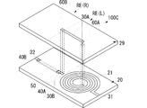
- FIGS. 9 and 10 are external perspective views showing the configuration of an LR series circuit using a conventional spiral electrode.
- the spiral electrode 21 is realized by a rewiring layer formed on the mounting surface side of the Si substrate 20.
- the rewiring layer including the spiral electrode 21 is formed on the Si substrate 20 via an insulating material portion 29 made of a passivation layer, an insulating protective layer, or the like.
- the outer peripheral end of the spiral electrode 21 is connected to the wiring electrode 31, and the inner peripheral end is connected to a via hole 60 formed in the insulating material portion 29.
- the via hole 60 has a shape penetrating the insulating material portion 29, and an end opposite to the connection end to the spiral electrode 21 is connected to one end of the wiring electrode 30 formed on the Si substrate 20.
- the wiring electrode 30 is formed in a shape such that the other end does not overlap the spiral electrode 21 in a state where the Si substrate 20 and the spiral electrode 21 are viewed in plan.
- the other end of the wiring electrode 30 is connected to one end of a resistor formed of the doping layer 50 through the contact hole 40A, as in FIG.
- the other end of this resistor is connected to the wiring electrode 32 on the Si substrate 20 through the contact hole 40B.
- the spiral electrode 21 is formed on the Si substrate 20.
- the outer peripheral end of the spiral electrode 21 is connected to a wiring electrode 31 formed on the Si substrate 20.
- the inner peripheral end of the spiral electrode 21 is connected to one end of the wiring electrode 30A of the rewiring layer via a via hole 60A formed in the insulating material portion 29, and the other end of the wiring electrode 30A is connected to the via hole 60B.
- the other end of the wiring electrode 30B is connected to one end of a resistor formed of the doping layer 50 through the contact hole 40A, as in FIG.
- the other end of this resistor is connected to the wiring electrode 32 on the Si substrate 20 through the contact hole 40B.
- An object of the present invention is to form an electronic circuit device including an inductor having a high inductance in a smaller size.
- the present invention relates to an electronic circuit device formed by forming an electronic circuit pattern using a semiconductor substrate.
- the electronic circuit device includes a series circuit of an inductor and a resistor.
- the inductor is formed from a spiral electrode pattern formed on the surface of the semiconductor substrate.
- One end of the resistor is connected to the inner peripheral end of the spiral electrode.
- the other end of the resistor reaches the outside of the spiral electrode winding region.
- the resistor itself is formed by a polycrystalline region or a doping region formed inside the spiral electrode formation surface side of the semiconductor substrate.
- the inner peripheral end of the inductor is formed on the same Si substrate surface as the spiral electrode via a resistor formed in the Si substrate. Connected to the wiring electrode.
- the inductor formed of the spiral electrode can be connected to another circuit element without using a rewiring layer or multilayer wiring. That is, an electronic circuit device including an inductor capable of obtaining a high inductance value can be formed at a low profile and at a low cost.
- the LR series circuit can be reduced in size. Realized in area. That is, an LR series circuit including an inductor capable of realizing a high inductance is realized with a small size (low profile and small area).
- the semiconductor substrate is a silicon substrate, and the polycrystalline region is a polysilicon region.
- the silicon substrate includes an insulating layer on the spiral electrode forming surface side.
- the insulating layer includes a contact hole that conducts between one end of the resistor and the inner peripheral end of the spiral electrode.
- This configuration shows a specific connection configuration between the above-described spiral electrode (inductor) on the surface of the Si substrate and a resistor inside the Si substrate, and is provided on an insulating layer used in the structure of a normal Si substrate.
- the contact hole realizes the connection between the inductor and the resistor.
- the electronic circuit device of the present invention further includes a rectifying element.
- the semiconductor substrate is a silicon substrate, and the rectifying element is realized by forming a pn junction region by providing a doping region in the silicon substrate.
- this electronic circuit device is provided with the wiring electrode formed in the silicon substrate surface which conducts this rectifier and at least one of a resistor or an inductor.
- This configuration shows a configuration of an electronic circuit device in which other circuit elements are added to the above-described LR series circuit.
- a rectifying element is formed using a pn junction region formed in a silicon substrate and connected to an LR series circuit.
- the electronic circuit device of the present invention further includes a capacitor.
- the capacitor is realized by providing a plurality of pn junction regions.
- this electronic circuit device is provided with the wiring electrode formed in the silicon substrate surface which conduct
- This configuration also shows the configuration of an electronic circuit device in which other circuit elements are added to the above-described LR series circuit.
- a capacitor is formed using a plurality of pn junction regions formed on the Si substrate, and connected to the LR series circuit.
- an electronic circuit device including an LR series circuit and a capacitor, for example, a resonant circuit using an LCR can be realized in a small size.
- the electronic circuit device of the present invention further includes an ESD element.
- the ESD element is realized by providing a plurality of pn junction regions. And this electronic circuit device is provided with the wiring electrode formed in the silicon substrate surface which conduct
- This configuration also shows the configuration of an electronic circuit device in which other circuit elements are added to the above-described LR series circuit.
- an ESD element is formed using a plurality of pn junction regions formed on a Si substrate and connected to an LR series circuit.
- an ESD protection device including an LR series circuit and an ESD element can be realized in a small size.
- the silicon substrate is appropriately referred to as a Si substrate depending on the case.
- an electronic circuit device including an inductor formed of a spiral electrode capable of realizing a high inductance can be formed in a small size.
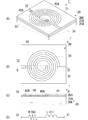
- FIG. 1 is a diagram showing a structure of an LR circuit device 1 that is an electronic circuit device of the present embodiment, in which FIG. 1A is an external perspective view seen from the side on which an inductor L is formed, and FIG. FIG. 1C is a cross-sectional view taken along the line AA ′ of FIG. 1B, and FIG. 1D is an equivalent circuit diagram of the LR circuit device 1 as viewed from the surface on which the inductor L is formed.
- the LR circuit device 1 of this embodiment includes a Si substrate 20 that can form an integrated circuit including the LR circuit device 1.
- the Si substrate 20 includes a Si base material portion 20A serving as a base material and a SiO 2 insulating layer 20B formed on the surface of the Si base material portion 20A.
- the Si base portion 20A is doped p-type or n-type. In the following, the case of the p-type is shown as an example, but the configuration of the present embodiment can be similarly realized even with the n-type.
- a spiral electrode 21 made of a metal thin film such as AL is formed on the surface of the Si substrate 20, that is, the surface of the insulating layer 20B.
- the electrode width and electrode length of the spiral electrode 21 are set to values at which desired inductance can be obtained.
- An inductor L is formed by the spiral electrode.
- the outer peripheral end of the spiral electrode 21 is connected to a wiring electrode 31 that is also formed on the surface of the Si substrate 20.
- Contact holes 40A and 40B are formed in the insulating layer 20B of the Si substrate 20.
- the contact holes 40A and 40B are made of a material having a predetermined conductivity that penetrates the insulating layer 20B.
- the contact hole 40 ⁇ / b> A is formed in an electrode formation region having a predetermined area on the inner peripheral end side of the spiral electrode 21.
- the contact hole 40B is a region where the spiral electrode 21 is formed, that is, a region outside the electrode group formed in a wound shape in plan view of the Si substrate 20, and at a position spaced apart from the contact hole 40A by a predetermined distance. Is formed.
- n + doping layer 51 having a predetermined length, a predetermined width, and a predetermined depth is formed in the Si base portion 20A of the Si substrate 20 so as to include the formation regions of the contact holes 40A, 40B.
- Such an n + doping layer 51 functions as a resistor R because it has a predetermined resistivity.
- the resistance value of this resistor can be set by the formation conditions of the n + doping layer 51, that is, the doping concentration, the total length (corresponding to the distance between the contact holes 40A and 40B), the total width, and the depth.
- the n + doping layer 51 is connected to the wiring electrode 32 formed on the surface of the Si substrate 20 through the contact hole 40B.
- an LR series circuit in which an inductor L and a resistor R are connected in series as shown in FIG. And by using such a structure, even if it comprises the inductor which consists of a spiral electrode, it is not necessary to use a rewiring layer like the past, and can make it low-profile. Further, since the spiral electrode is used instead of the meander electrode, the inductance can be increased per unit area. Thereby, an inductor having a high inductance can be formed in a small area with a low profile and at a low cost.
- the resistor connected in series to the inductor can be formed so as to overlap with the inductor in plan view, the LR series circuit composed of the inductor and the resistor can be formed with a small area. That is, the electronic circuit device of the LR series circuit can be formed smaller than before.
- FIG. 2A and 2B are diagrams illustrating the structure of the LR circuit device 1 ′ according to the present embodiment.
- FIG. 2A is an external perspective view as viewed from the formation surface side of the inductor L
- FIG. 2C is a cross-sectional view taken along the line BB ′ of FIG. 2B
- FIG. 2D is an equivalent circuit diagram of the LR circuit device 1 ′.
- the resistor R is formed not by the doping layer shown in the first embodiment but by the polysilicon layer 50.
- the Si substrate 20 of the present embodiment includes a Si base portion 20A as a base material and SiO 2 insulating layers 20B and 20C formed on the surface of the Si base portion 20A.
- the Si base portion 20A may be the same as that of the first embodiment or may be an intrinsic semiconductor.
- a spiral electrode 21 made of a metal thin film such as AL is formed on the surface of the Si substrate 20, that is, the surface of the insulating layer 20C.
- the structure of the spiral electrode 21 is the same as that in the first embodiment.
- the outer peripheral end of the spiral electrode 21 is connected to a wiring electrode 31 that is also formed on the surface of the Si substrate 20.
- Contact holes 40A and 40B are formed in the insulating layer 20C, which is the outermost surface layer of the Si substrate 20.
- the contact holes 40A and 40B are made of a material having a predetermined conductivity that penetrates the insulating layer 20C.
- the contact hole 40 ⁇ / b> A is formed in an electrode formation region having a predetermined area on the inner peripheral end side of the spiral electrode 21.
- the contact hole 40B is a region where the spiral electrode 21 is formed, that is, a region outside the group of electrodes formed in a wound shape in plan view of the Si substrate 20, and at a position spaced apart from the contact hole 40A by a predetermined distance. Is formed.
- a polysilicon layer 50 having a predetermined length and a predetermined width is formed in the insulating layer 20B sandwiched between the Si base portion 20A and the insulating layer 20C of the Si substrate 20 so as to include the formation regions of the contact holes 40A and 40B. . Since such a polysilicon layer 50 has a predetermined resistivity, it functions as a resistor R. The resistance value of this resistor can be set according to the formation conditions of the polysilicon layer 50, that is, the total length (corresponding to the distance between the contact holes 40A and 40B) and the total width.
- the polysilicon layer 50 is connected to the wiring electrode 32 formed on the surface of the Si substrate 20 through the contact hole 40B.
- an LR series circuit in which an inductor L and a resistor R are connected in series as shown in FIG. 2D can be realized as in FIG.
- an electronic circuit device of an LR series circuit using an inductor having a high inductance per unit area can be formed smaller than the conventional one, as in the first embodiment. .
- any one of a vapor deposition method, a sputtering method, and a CVD method is used as a method for forming the polysilicon layer.
- FIG. 3A and 3B are diagrams showing the structure of the RLR circuit device 1 ′′ according to the present embodiment, in which FIG. 3A is an external perspective view seen from the formation surface side of the inductor L, and FIG. FIG. 3C is a sectional view taken along the line BB ′ of FIG. 3B, FIG. 3D is a sectional view taken along the line CC ′ of FIG. 3B, and FIG. ) Is an equivalent circuit diagram of the RLR circuit device 1 ′′.
- the RLR circuit device 1 ′′ of this embodiment is obtained by further connecting a resistor in series to the outer peripheral end side of the spiral electrode 21 of the LR circuit device 1 ′ shown in the second embodiment.
- the description of the configuration of the inductor L and the resistor Ra including the polysilicon layer 50A connected to the inner peripheral end of the spiral electrode 21 and the configuration of the contact holes 40A and 40B will be omitted.
- a contact hole 40 ⁇ / b> C is formed in an electrode forming region having a predetermined area on the outer peripheral end side of the spiral electrode 21. Further, a contact hole 40D is formed at a predetermined distance from the contact hole 40C.
- a polysilicon layer 50B having a predetermined length and a predetermined width is formed on the insulating layer 20B of the Si substrate 20 so as to include the formation regions of the contact holes 40C and 40D.
- This polysilicon layer 50B functions as a resistor Rb.
- the polysilicon layer 50 ⁇ / b> B is desirably formed so that the extending direction (length direction) coincides with the tangential direction at the outer peripheral end of the spiral electrode 21.
- the polysilicon layer 50B is connected to the wiring electrode 31 formed on the surface of the Si substrate 20 through the contact hole 40D.
- the RLR series circuit which consists of these inductors and two resistors can be formed with a small area. That is, the electronic circuit device of the RLR series circuit can be formed smaller than the conventional one. Furthermore, if the extending direction of the polysilicon layer 50B connected to the outer peripheral end of the spiral electrode 21 is made to coincide with the tangential direction at the outer peripheral end of the spiral electrode 21, the RLR circuit device can be formed more compactly.
- each resistor may be formed by a doping layer as shown in the first embodiment.
- each resistor may be formed of a polysilicon layer and a doping layer according to the specification of the resistance value.
- FIG. 4A and 4B are diagrams showing the structure of the ESD protection device 10 according to the present embodiment.
- FIG. 4A is an external perspective view seen from the surface on which the inductor L is formed
- FIG. 4B is FIG.
- FIG. 4C is an equivalent circuit diagram of the ESD protection device 10.
- the ESD protection device 10 of the present embodiment is obtained by further connecting an ESD protection element ESD in series to the outer peripheral end side of the spiral electrode 21 of the RLR circuit device 1 ′′ shown in the third embodiment.
- the resistors Ra and Rb thus, the configuration of the inductor L formed of the spiral electrode 21 and the resistors Ra and Rb formed of the doping layers 51A and 51B and the configurations of the contact holes 40A to 40D are as follows. Description is omitted.
- a wiring electrode 33 is formed on the outer peripheral end of the spiral electrode 21 so as to be continuous with the spiral electrode 21.
- a contact hole 41 ⁇ / b> A is formed in an electrode formation region having a predetermined area opposite to the spiral electrode 21 side of the wiring electrode 33. Furthermore, a contact hole 41B is formed at a predetermined distance from the contact hole 41A.
- the contact holes 41A and 41B are made of a material having a predetermined conductivity that penetrates the insulating layer 20B.
- n + doping layers 80A and 80B are formed with a predetermined area and a predetermined depth so as to include the formation regions of the contact holes 41A and 41B. At this time, the n + doping layers 80A and 80B are formed with a predetermined width. Further, a p well layer 81 is formed in the Si base portion 20A so as to include these n + doping layers 80A and 80B.
- the contact hole 41B formed on the n + doping layer 80B is connected to the wiring electrode 34 formed on the surface of the Si substrate 20.
- the resistor Ra, the inductor L, and the resistor Rb as shown in FIG. 4C are connected in series to the RLR series circuit in this order, and the connection point between the inductor L and the resistor Rb is connected.
- the ESD protection element ESD the T-type ESD protection device 10 can be realized. And by using such a structure, an ESD protection device can be formed smaller than before.
- the ESD protection element ESD functions as a capacitor Ce as long as it is not in the ON state.
- a T-type RLCR low pulse filter can be formed.
- FIG. 5 is a graph showing the pass characteristic (S21 characteristic) of the T-type RLCR low-pass filter of the present embodiment.
- the thick solid line shows the configuration of the present embodiment, that is, the inductor L is formed by a spiral electrode.
- a thin broken line indicates a case where the inductor L is formed by a conventional meander electrode (meander electrode).
- the shape is kept smaller than when a conventional meander electrode is used, but at a frequency closer to the passband and sharper. Attenuation poles can be formed with characteristics.
- FIG. 6A and 6B are diagrams illustrating the structure of the LCR resonant circuit device 11 according to the present embodiment, in which FIG. 6A is an external perspective view seen from the formation surface side of the inductor L, and FIG. 6B is the LCR resonant circuit device 11.
- FIG. 6A is an external perspective view seen from the formation surface side of the inductor L
- FIG. 6B is the LCR resonant circuit device 11.
- the configuration of the spiral electrode 21, the wiring electrode 31, and the contact hole 40A is the same, and the description thereof is omitted.
- a wiring electrode 33 is formed on the outer peripheral edge of the spiral electrode 21 on the surface of the Si substrate 20 so as to be continuous with the spiral electrode 21.
- a contact hole 41 ⁇ / b> A is formed in an electrode formation region having a predetermined area opposite to the spiral electrode 21 side of the wiring electrode 33. Furthermore, a contact hole 41B is formed at a predetermined distance from the contact hole 41A.
- the contact holes 41A and 41B are made of a material having a predetermined conductivity that penetrates the insulating layer 20B.
- a wiring electrode 34 is formed on the surface of the Si substrate 20 corresponding to the formation region of the contact hole 41B.
- n + doping layers 80A and 80B are formed with a predetermined area and a predetermined depth so as to include the formation regions of the contact holes 41A and 41B. At this time, the n + doping layers 80A and 80B are formed with a predetermined width.
- the n + doping layer 52 having a predetermined length, a predetermined width, and a predetermined depth so that the formation region of the contact hole 40A and the formation region of the contact hole 41B are both ends. Is formed. At this time, as shown in FIG. 6, the n + doping layer 52 and the n + doping layer 80B are integrally formed.
- the n + doping layer 52 between the contact holes 40A and 41B functions as the resistor Ra
- a series of pn junction structures between the contact holes 41A and 41B function as the capacitor C.
- an LCR resonant circuit device is formed in which the wiring electrodes 31 and 34 are input / output terminals, and the series circuit of the inductor L and the resistor Ra and the capacitor C are connected in parallel. be able to.
- the example in which the n + doping layers 52 and 80B are integrated and the wiring electrode 34 is formed by a single electrode is shown.
- the wiring electrode 34 is formed in a bifurcated shape, and each terminal portion is formed.
- the n + doping layers 52 and 80B may be formed separated from each other by a predetermined distance so as to be connected to each contact hole.
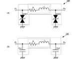
- FIG. 7 is an equivalent circuit diagram showing a ⁇ -type ESD protection device and a ⁇ -type low-pass filter.
- FIG. 7A is an equivalent circuit diagram of a ⁇ -type ESD protection device
- FIG. 7B is an equivalent circuit diagram of a ⁇ -type CRLC low-pass filter.
- a resistor R and an inductor L are connected in series between an input port Pi and an output port Po. Both ends of the LR series circuit are connected to the ground by ESD protection elements ESD1 and ESD2.
- a resistor R and an inductor L are connected in series between an input terminal Pi and an output port Po. Both ends of the LR series circuit are connected to the ground by capacitors Ce1 and Ce2.
- LR series circuits shown in FIGS. 7A and 7B can be realized by using the configurations of the first and second embodiments for these electronic circuits, for example. Further, a series of pn junction structures formed on the outer peripheral end side of the spiral electrode 21 shown in FIG. 4 of the fourth embodiment are arranged at the position of the contact hole 40B of the wiring electrode 32 shown in FIGS. If formed in the vicinity of the contact hole 40B, an L-type circuit composed of the LR series circuit shown in FIGS. 7A and 7B and one ESD element or one capacitor can be realized.
- the semiconductor substrate is a Si substrate and the polycrystal is polysilicon.
- the configuration of the present invention can be applied to a semiconductor substrate other than the Si substrate and a polycrystal other than polysilicon. . That is, it can be applied to a semiconductor substrate made of germanium, GaAs, InP, ZnTe, or the like.
- the present invention can also be applied to a polycrystal composed of Ta 2 O 5 .
Landscapes
- Semiconductor Integrated Circuits (AREA)
Abstract
Si基板(20)の表面にはスパイラル電極(21)が形成されている。スパイラル電極(21)の外周端は配線電極(31)に導通している。Si基板(20)の表層である絶縁層(20B)におけるスパイラル電極(21)の内周端に対応する領域には、コンタクトホール(40A)が形成されている。また、絶縁層(20B)におけるスパイラル電極(21)の巻回領域よりも外部側の所定位置にもコンタクトホール(40B)が形成されている。このコンタクトホール(40B)は、Si基板(20)の表面の配線電極(32)に導通している。Si基板(20)のSi基材部(20A)における、コンタクトホール(40A、40B)を両端とする略直方体形状の領域にはn+ドーピング層(51)が形成されている。このn+ドーピング層がスパイラル電極(21)の引き出し電極であり、且つ抵抗器として機能する。
Description
本発明は、インダクタや抵抗等により回路形成された電子回路デバイス、特に、半導体基板を用いて回路形成された電子回路デバイスに関するものである。
現在、携帯端末等に利用する電子回路は小型化が要求されており、当該小型化を実現するために、CSP(Chip Size Package)のような集積化された電子デバイスが多く利用されている。このような集積化された電子デバイスに利用するインダクタは、Si基板上に所定パターンで電極を形成することにより実現される。例えば、特許文献1では、Si基板上にミアンダ形状の電極(ミアンダ電極)を形成することで、インダクタを実現している。このようなミアンダ電極のインダクタを用いたLR直列回路の構成を図8に示す。図8は、従来のSi基板を用いて、ミアンダ電極のインダクタを用いたLR直列回路100Aの構造を示す外観斜視図である。
図8に示すように、Si基板20は、詳細な構成は図示しないが、母材となるSi基材部と、その表面のSiO2からなる絶縁層と、を備える。Si基板20の表面には、Al等の電極膜からなるインダクタ200がミアンダ形状で形成されている。当該インダクタ200の一方端は、配線電極300Aに接続し、他方端は、SiO2の絶縁膜に形成されたコンタクトホール40Aに接続している。このコンタクトホール40Aに対して、インダクタ200と反対側に所定距離の位置には、もう一個のコンタクトホール40Bが形成されおり、当該コンタクトホール40Bは配線電極300Bに接続している。そして、これらコンタクトホール40A,40B間のSi基材部は、所定の不純物によりドーピングされたドーピング層50が形成され、当該ドーピング層50が抵抗器として機能する。
しかしながら、上述のミアンダ形状のインダクタは、面積当たりに稼げるインダクタンスが小さく、集積化された電子デバイスのSi基板上に形成するような場合には、必要とするインダクタンスを得ることができないことがある。また、このインダクタと抵抗器とを直列接続したLR直列回路を形成する場合、さらに広い面積を有することになる。
このように、従来のミアンダ形状のインダクタを用いたLR直列回路は、広いスペースを必要とし、さらにインダクタンスを高くしようとすれば、ミアンダ形状をさらに延長しなければならず、より一層広いスペースを必要としてしまう。
このため、ミアンダ形状よりも単位面積当たりのインダクタンスが高い、スパイラル形状の電極(スパイラル電極)を用いたインダクタを採用することも可能である。
ところが、このようなスパイラル電極は、一方端が巻回される電極群の最内周にあるので、Si基板上の電極が一層構造である場合には、当該内周端を他の電極へ直接に接続することはできない。
例えば、スパイラル電極によるインダクタと抵抗器とからなるLR直列回路を形成する場合、従来では図9や図10の構成が用いられる。図9、図10は従来のスパイラル電極を用いたLR直列回路の構成を示す外観斜視図である。
図9のLR直列回路100Bでは、スパイラル電極21を、Si基板20の実装面側に形成した再配線層によって実現している。このスパイラル電極21を含む再配線層は、パッシべーション層や絶縁性の保護層等からなる絶縁材部29を介して、Si基板20上に形成される。スパイラル電極21の外周端は配線電極31に接続しており、内周端は絶縁材部29に形成されたビアホール60に接続している。ビアホール60は絶縁材部29を貫通する形状からなり、スパイラル電極21への接続端と反対側の端部が、Si基板20上に形成された配線電極30の一方端へ接続している。配線電極30は、Si基板20とスパイラル電極21を平面視した状態で、他方端がスパイラル電極21と重ならないような形状で、形成されている。配線電極30の他方端は、図8と同様に、コンタクトホール40Aを介してドーピング層50からなる抵抗器の一方端部に接続する。この抵抗器の他方端部は、コンタクトホール40Bを介してSi基板20上の配線電極32に接続する。
また、図10のLR直列回路100Cでは、スパイラル電極21を、Si基板20上に形成する。スパイラル電極21の外周端は、Si基板20上に形成された配線電極31に接続する。一方、スパイラル電極21の内周端は、絶縁材部29に形成されたビアホール60Aを介して再配線層の配線電極30Aの一方端に接続し、当該配線電極30Aの他方端はビアホール60Bを介して、Si基板20上の配線電極30Bの一方端に接続している。配線電極30Bの他方端は、図9と同様に、コンタクトホール40Aを介してドーピング層50からなる抵抗器の一方端部に接続する。この抵抗器の他方端部は、コンタクトホール40Bを介してSi基板20上の配線電極32に接続する。
このように従来では、スパイラル電極を用いようとすると、必ず再配線層や多層配線を用いる等、Si基板の表面上に二層構造を設けなければならなかった。そして、このような構造で用いられる再配線層は、通常Si基板表面の電極膜よりも厚く、絶縁材部の厚みも或程度必要とするので、低背化に対して制約となったり、低コスト化への妨げになっていた。さらに、ミアンダ電極やスパイラル電極からなるインダクタ素子の形成領域と抵抗器との形成領域を分ける必要があった。このため、高いインダクタンスを有するインダクタを備えた電子回路デバイスを形成する場合、面積的にも小型化に制約があった。
この発明の目的は、高いインダクタンスを有するインダクタを備えた電子回路デバイスを、より小型に形成することにある。
(1)この発明は、半導体基板を用いて電子回路パターンを形成してなる電子回路デバイスに関するものである。この電子回路デバイスは、インダクタと抵抗器との直列回路を備える。インダクタは、半導体基板表面に形成されたスパイラル形状の電極パターンから形成される。抵抗器の一方端はスパイラル電極の内周端に接続する。抵抗器の他方端はスパイラル電極の巻回領域よりも外部に達する。そして、抵抗器自身は、半導体基板におけるスパイラル電極の形成面側の内部に形成された多結晶領域もしくはドーピング領域により形成される。
この構成では、スパイラル電極からなるインダクタをSi基板表面で形成しても、当該インダクタの内周端は、Si基板内に形成された抵抗器を介して、スパイラル電極と同じSi基板表面に形成された配線電極に接続される。これにより、再配線層や多層配線を用いずとも、スパイラル電極からなるインダクタを他の回路素子へ接続できる。すなわち、高いインダクタンス値を得られるインダクタを含む電子回路デバイスを低背且つ低コストに形成できる。さらに、インダクタの内周端が、他の回路素子への配線電極へ導通する抵抗器がSi基板を平面視して、スパイラル電極の形成領域と重なる領域に形成されるので、LR直列回路を小さな面積で実現できる。すなわち、高いインダクタンスを実現できるインダクタを備えるLR直列回路が小型(低背、小面積)で実現される。
(2)また、この発明の電子回路デバイスは、半導体基板がシリコン基板であり、多結晶領域がポリシリコン領域である。そして、シリコン基板は、スパイラル電極の形成面側に絶縁層を備える。この絶縁層は、抵抗器の一方端とスパイラル電極の内周端とを導通するコンタクトホールを備える。
この構成では、上述のSi基板表面のスパイラル電極(インダクタ)とSi基板内部の抵抗器との具体的接続構成を示すものであり、通常のSi基板の構造で利用されている絶縁層に設けたコンタクトホールによって、インダクタと抵抗器との接続を実現している。
(3)また、この発明の電子回路デバイスは整流素子をさらに備える。半導体基板がシリコン基板であり、整流素子は、シリコン基板にドーピング領域を設けることでpn接合領域を形成して実現する。そして、この電子回路デバイスは、該整流素子と抵抗器もしくはインダクタの少なくとも一方とを導通するシリコン基板表面に形成された配線電極を備える。
この構成では、上述のLR直列回路に対して、他の回路素子を付加した電子回路デバイスの構成を示すものである。この電子回路デバイスでは、シリコン基板に形成されたpn接合領域を利用して整流素子を形成し、LR直列回路へ接続する。これにより、LR直列回路と整流素子を備える電子回路デバイスを小型に実現できる。
(4)また、この発明の電子回路デバイスは、キャパシタをさらに備える。キャパシタは、pn接合領域を複数設けることで実現される。そして、この電子回路デバイスは、キャパシタと抵抗器もしくはインダクタの少なくとも一方とを導通するシリコン基板表面に形成された配線電極を備える。
この構成も、上述のLR直列回路に対して、他の回路素子を付加した電子回路デバイスの構成を示すものである。この電子回路デバイスでは、Si基板に形成された複数のpn接合領域を利用してキャパシタを形成し、LR直列回路へ接続する。これにより、LR直列回路とキャパシタを備える電子回路デバイス、例えばLCRを用いた共振回路等を小型に実現できる。
(5)また、この発明の電子回路デバイスは、ESD素子をさらに備える。ESD素子は、pn接合領域を複数設けることで実現される。そして、この電子回路デバイスは、ESD素子と抵抗器もしくはインダクタの少なくとも一方とを導通するシリコン基板表面に形成された配線電極を備える。
この構成も、上述のLR直列回路に対して、他の回路素子を付加した電子回路デバイスの構成を示すものである。この電子回路デバイスでは、Si基板に形成された複数のpn接合領域を利用してESD素子を形成し、LR直列回路へ接続する。これにより、LR直列回路とESD素子を備えるESD保護デバイスを小型に実現できる。なお、この明細書においては、場合に応じて、シリコン基板をSi基板と適宜称することとする。
この発明によれば、高いインダクタンスを実現できるスパイラル電極で形成されたインダクタを含む電子回路デバイスを、小型に形成することができる。
本発明の第1の実施形態に係る電子回路デバイスについて、図を参照して説明する。図1は、本実施形態の電子回路デバイスであるLR回路デバイス1の構造を示す図であり、図1(A)がインダクタLの形成面側から見た外観斜視図、図1(B)がインダクタLの形成面側を見た平面図、図1(C)が図1(B)のA-A’断面図、図1(D)がLR回路デバイス1の等価回路図である。
本実施形態のLR回路デバイス1は、当該LR回路デバイス1を含む集積回路を形成可能なSi基板20を備える。Si基板20は、母材となるSi基材部20Aと、当該Si基材部20Aの表面に形成されたSiO2の絶縁層20Bとからなる。Si基材部20Aは、p型もしくはn型にドーピングされている。なお、以下では、p型の場合を例に示すが、n型であっても、同様に本実施形態の構成を実現できる。
Si基板20の表面すなわち絶縁層20Bの表面には、AL等の金属薄膜からなるスパイラル形状の電極21が形成されている。このスパイラル電極21の電極幅および電極長は、所望とするインダクタンスが得られる値に設定されている。このスパイラル電極によりインダクタLが形成される。当該スパイラル電極21の外周端は、同じくSi基板20の表面に形成された配線電極31に接続されている。
Si基板20の絶縁層20Bには、コンタクトホール40A,40Bが形成されている。コンタクトホール40A,40Bは、絶縁層20Bを貫通する所定導電率の材料からなる。コンタクトホール40Aは、スパイラル電極21の内周端側における所定面積の電極形成領域に形成されている。一方、コンタクトホール40Bは、スパイラル電極21の形成領域すなわちSi基板20を平面視して巻回形に形成された電極群よりも外側の領域で、且つコンタクトホール40Aから所定距離離間された位置に形成されている。
Si基板20のSi基材部20Aには、コンタクトホール40A,40Bの形成領域を含むように所定長、所定幅、および所定深さでn+ドーピング層51が形成されている。このようなn+ドーピング層51は、所定の抵抗率を有するので、抵抗器Rとして機能する。なお、この抵抗器の抵抗値は、n+ドーピング層51の形成条件、すなわちドープ濃度、全長(コンタクトホール40A,40B間の距離に対応)、全幅、深さにより、設定することができる。このn+ドーピング層51は、コンタクトホール40Bを介して、Si基板20の表面に形成された配線電極32に接続されている。
このような構成とすれば、図1(D)に示すようなインダクタLと抵抗器Rとが直列接続されたLR直列回路を実現できる。そして、このような構成を用いることで、スパイラル電極からなるインダクタを構成しても、従来のように再配線層を用いなくてもよく、低背化することができる。また、ミアンダ電極でなくスパイラル電極であるので、単位面積当たりにインダクタンスを高くすることができる。これにより、高いインダクタンスを有するインダクタを小さい面積で低背且つ低コストで形成することができる。
さらに、このインダクタに直列接続する抵抗器を、平面視してインダクタと重なるように形成できるので、これらインダクタと抵抗器とからなるLR直列回路を小さい面積で形成することができる。すなわち、LR直列回路の電子回路デバイスを、従来よりも小型に形成することができる。
次に、第2の実施形態に係る電子回路デバイスであるLR回路デバイスについて、図を参照して説明する。図2は、本実施形態のLR回路デバイス1’の構造を示す図であり、図2(A)がインダクタLの形成面側から見た外観斜視図、図2(B)がインダクタLの形成面側を見た平面図、図2(C)が図2(B)のB-B’断面図、図2(D)がLR回路デバイス1’の等価回路図である。
本実施形態のLR回路デバイス1’は、抵抗器Rを、第1の実施形態に示したドーピング層で形成するのではなく、ポリシリコン層50で形成するものである。
本実施形態のSi基板20は、母材となるSi基材部20Aと、当該Si基材部20Aの表面に形成されたSiO2の絶縁層20B,20Cとからなる。Si基材部20Aは、第1の実施形態と同じであってもよく、真性半導体であってもよい。
Si基板20の表面すなわち絶縁層20Cの表面には、AL等の金属薄膜からなるスパイラル形状の電極21が形成されている。なお、スパイラル電極21の構造は、第1の実施形態と同じである。当該スパイラル電極21の外周端は、同じくSi基板20の表面に形成された配線電極31に接続している。
Si基板20の最表面層である絶縁層20Cには、コンタクトホール40A,40Bが形成されている。コンタクトホール40A,40Bは、絶縁層20Cを貫通する所定導電率の材料からなる。コンタクトホール40Aは、スパイラル電極21の内周端側における所定面積の電極形成領域に形成されている。一方、コンタクトホール40Bは、スパイラル電極21の形成領域すなわちSi基板20を平面視して巻回形に形成された電極群よりも外側の領域で、且つコンタクトホール40Aから所定距離離間された位置に形成されている。
Si基板20のSi基材部20Aと絶縁層20Cに挟まれた絶縁層20Bには、コンタクトホール40A,40Bの形成領域を含むように所定長で所定幅のポリシリコン層50が形成されている。このようなポリシリコン層50は、所定の抵抗率を有するので、抵抗器Rとして機能する。なお、この抵抗器の抵抗値は、ポリシリコン層50の形成条件、すなわち全長(コンタクトホール40A,40B間の距離に対応)および全幅により設定することができる。このポリシリコン層50は、コンタクトホール40Bを介して、Si基板20の表面に形成された配線電極32に接続されている。
このような構成としても、図1(D)と同じように、図2(D)に示すようなインダクタLと抵抗器Rとが直列接続されたLR直列回路を実現できる。そして、このような構成を用いることで、第1の実施形態と同様に、単位面積当たりのインダクタンスが高いインダクタを用いたLR直列回路の電子回路デバイスを、従来よりも小型に形成することができる。
なお、ポリシリコン層を形成する方法として、蒸着法、スパッタリング法およびCVD法のいずれかの方法を用いる。
次に、第3の実施形態に係る電子回路デバイスであるLR回路デバイスについて、図を参照して説明する。図3は、本実施形態のRLR回路デバイス1”の構造を示す図であり、図3(A)がインダクタLの形成面側から見た外観斜視図、図3(B)がインダクタLの形成面側を見た平面図、図3(C)が図3(B)のB-B’断面図、図3(D)が図3(B)のC-C’断面図、図3(E)がRLR回路デバイス1”の等価回路図である。
本実施形態のRLR回路デバイス1”は、第2の実施形態に示したLR回路デバイス1’のスパイラル電極21の外周端側にさらに抵抗器を直列接続したものである。したがって、スパイラル電極21からなるインダクタLと、当該スパイラル電極21の内周端側に接続されたポリシリコン層50Aからなる抵抗器Raとの構成やコンタクトホール40A,40Bの構成については、説明を省略する。
Si基板20の最表面層である絶縁層20Cには、スパイラル電極21の外周端側における所定面積の電極形成領域に、コンタクトホール40Cが形成されている。さらに、当該コンタクトホール40Cから所定距離の位置にコンタクトホール40Dが形成されている。
Si基板20の絶縁層20Bには、コンタクトホール40C,40Dの形成領域を含むように所定長、所定幅でポリシリコン層50Bが形成されている。このポリシリコン層50Bが抵抗器Rbとして機能する。この際、ポリシリコン層50Bは、伸延方向(長さ方向)がスパイラル電極21の外周端における接線方向と一致するように形成することが望ましい。そして、このポリシリコン層50Bは、コンタクトホール40Dを介して、Si基板20の表面に形成された配線電極31に接続されている。
このような構成とすれば、図3(E)に示すような抵抗器Ra、インダクタL、および抵抗器Rbが直列接続されたRLR直列回路を実現できる。そして、このような構成を用いることで、これらインダクタと二個の抵抗器とからなるRLR直列回路を小さい面積で形成することができる。すなわち、RLR直列回路の電子回路デバイスを、従来よりも小型に形成することができる。さらに、スパイラル電極21の外周端に接続するポリシリコン層50Bの伸延方向を、スパイラル電極21の外周端における接線方向に一致させれば、RLR回路デバイスを、より小型に形成することができる。
なお、本実施形態では、ポリシリコン層を用いて抵抗器を形成する例を示したが、第1の実施形態に示すようなドーピング層により、それぞれの抵抗器を形成してもよい。
また、抵抗値の仕様に応じて、それぞれの抵抗器を、ポリシリコン層とドーピング層のそれぞれで形成してもよい。
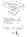
次に、第4の実施形態に係る電子回路デバイスであるESD保護デバイスについて、図を参照して説明する。図4は、本実施形態のESD保護デバイス10の構造を示す図であり、図4(A)がインダクタLの形成面側から見た外観斜視図、図4(B)が図4(A)のD-D’断面図、図4(C)がESD保護デバイス10の等価回路図である。
本実施形態のESD保護デバイス10は、第3の実施形態に示したRLR回路デバイス1”のスパイラル電極21の外周端側にさらにESD保護素子ESDを直列接続したものであり、抵抗器Ra,Rbをドーピング層51A,51Bで形成したものである。したがって、スパイラル電極21からなるインダクタLと、ドーピング層51A,51Bからなる抵抗器Ra,Rbとの構成やコンタクトホール40A~40Dの構成については、説明を省略する。
スパイラル電極21の外周端には、当該スパイラル電極21に連続するように、配線電極33が形成されている。
Si基板20の絶縁層20Bには、配線電極33のスパイラル電極21側と反対側の所定面積の電極形成領域に、コンタクトホール41Aが形成されている。さらに、当該コンタクトホール41Aから所定距離の位置にコンタクトホール41Bが形成されている。コンタクトホール41A,41Bは、絶縁層20Bを貫通する所定導電率の材料からなる。
Si基板20のSi基材部20Aには、コンタクトホール41A,41Bの形成領域を含むように所定面積および所定深さでn+ドーピング層80A,80Bがそれぞれ形成されている。この際、n+ドーピング層80A,80B間は、所定幅で離間されるように形成されている。さらに、Si基材部20Aには、これらn+ドーピング層80A,80Bを含むようにpウェル層81が形成されている。
このような構成とすることで、コンタクトホール41A,41B間、すなわち、配線電極33,34間に、極性が逆のpn接合領域を連続して形成できる。これにより、配線電極33,34間に、極性が逆のダイオードを直列接続した回路が構成され、ESD保護素子ESDを形成することができる。
そして、このn+ドーピング層80B上に形成されたコンタクトホール41Bは、Si基板20の表面に形成された配線電極34に接続されている。
このような構成とすれば、図4(C)に示すような抵抗器Ra、インダクタL、抵抗器Rbの順に直列接続されたRLR直列回路と、インダクタLおよび抵抗器Rbの接続点に接続されたESD保護素子ESDとで、T型のESD保護デバイス10を実現することができる。そして、このような構成を用いることで、ESD保護デバイスを、従来よりも小型に形成することができる。
なお、このESD保護素子ESDは、ON状態にならない範囲であれば、キャパシタCeとして機能する。これにより、本実施形態の構成を用いれば、T型のR-L-C-Rローパルスフィルタを形成することもできる。
このローパスフィルタは、図5に示すような減衰極を形成することができる。図5は、本実施形態のT型のR-L-C-Rローパスフィルタの通過特性(S21特性)を示すグラフであり、太実線は本実施形態の構成すなわちスパイラル電極でインダクタLを形成した場合、細破線は従来のミアンダ電極(メアンダ電極)でインダクタLを形成した場合を示す。
図5に示すように、本実施形態のようなスパイラル電極でインダクタLを形成することで、従来のミアンダ電極を用いる場合より、形状を小さく抑えながらも、より通過帯域に近い周波数で且つ急峻な特性で減衰極を形成することができる。
次に、第5の実施形態に係る電子回路デバイスであるLCR共振回路について、図を参照して説明する。
図6は、本実施形態のLCR共振回路デバイス11構造を示す図であり、図6(A)がインダクタLの形成面側から見た外観斜視図、図6(B)がLCR共振回路デバイス11の等価回路図である。
上述の各実施形態では、抵抗器として機能するポリシリコン層やドーピング層を、スパイラル電極の内周端を基準にして、外周端と反対側の方向に伸延して形成する例を示したが、本実施形態では抵抗器として機能するポリシリコン層やドーピング層を外周端側に向けて形成した場合の一例を示す。なお、以下の説明では、ドーピング層で抵抗器を形成する場合を示すが、上述の各実施形態と同様に、ポリシリコン層で抵抗器を形成してもよい。
本実施形態のLCR共振回路デバイス11は、スパイラル電極21、配線電極31、コンタクトホール40Aの構成は同じであるので、説明は省略する。
Si基板20の表面におけるスパイラル電極21の外周端には、当該スパイラル電極21に連続するように、配線電極33が形成されている。
Si基板20の絶縁層20Bには、配線電極33のスパイラル電極21側と反対側の所定面積の電極形成領域に、コンタクトホール41Aが形成されている。さらに、当該コンタクトホール41Aから所定距離の位置にコンタクトホール41Bが形成されている。コンタクトホール41A,41Bは、絶縁層20Bを貫通する所定導電率の材料からなる。そして、コンタクトホール41Bの形成領域に対応するSi基板20の表面には、配線電極34が形成されている。
Si基板20のSi基材部20Aには、コンタクトホール41A,41Bの形成領域を含むように所定面積および所定深さでn+ドーピング層80A,80Bがそれぞれ形成されている。この際、n+ドーピング層80A,80B間は、所定幅で離間されるように形成されている。
さらに、Si基板20のSi基材部20Aには、コンタクトホール40Aの形成領域とコンタクトホール41Bの形成領域とを両端とするように、所定長、所定幅、および所定深さでn+ドーピング層52が形成されている。この際、図6に示すように、n+ドーピング層52と、上述のn+ドーピング層80Bとを一体形成する。
このような構成とすることで、コンタクトホール40A,41B間のn+ドーピング層52が抵抗器Raとして機能し、コンタクトホール41A,41B間の一連のpn接合構造がキャパシタCとして機能する。これにより、図6(B)に示すように、配線電極31,34を入出力端子とし、インダクタLおよび抵抗器Raの直列回路と、キャパシタCとが並列接続されたLCR共振回路デバイスを形成することができる。そして、本実施形態に示すような構成を用いることで、低背且つ小面積のLCR共振回路デバイスを実現することができる。
なお、本実施形態では、n+ドーピング層52,80Bを一体化し、配線電極34を一本の電極で形成する例を示したが、配線電極34を二分岐の形状で形成し、それぞれの終端部にコンタクトホールを設けて、各コンタクトホールにそれぞれ接続するように、n+ドーピング層52,80Bを所定距離離間して形成してもよい。
なお、上述の各実施形態の構成を用いれば、上記T型のESD保護デバイスやT型のR-L-C-Rローパスフィルタのみでなく、次に示すような他のESD保護デバイスや、フィルタを形成することもできる。
図7は、π型のESD保護デバイスおよびπ型のローパスフィルタを示す等価回路図である。図7(A)はπ型のESD保護デバイスの等価回路図であり、図7(B)はπ型のC-R-L-Cローパスフィルタの等価回路図である。
図7(A)に示すようなπ型のESD保護デバイス10Pは、入力ポートPiと出力ポートPoとの間に、抵抗器RとインダクタLとが直列接続されている。このLR直列回路の両端は、ESD保護素子ESD1,ESD2によりグランドに接続されている。
また、図7(B)に示すπ型のC-R-L-Cローパスフィルタ10Fは、入力端子Piと出力ポートPoとの間に、抵抗器RとインダクタLとが直列接続されている。このLR直列回路の両端は、キャパシタCe1,Ce2によりグランドに接続されている。
これらの電子回路に対して、例えば第1、第2の実施形態の構成を用いれば、図7(A),(B)に示すLR直列回路を実現できる。また、第4実施形態の図4に示したスパイラル電極21の外周端側に形成した一連のpn接合構造を、図1,図2に示す配線電極32のコンタクトホール40Bの位置または配線電極32におけるコンタクトホール40Bの近傍位置に形成すれば、図7(A),(B)に示すLR直列回路と一方のESD素子もしくは一方のキャパシタとのL型回路を実現することができる。
さらに、これらは一例を示すものであり、スパイラル電極とこれに直列接続する抵抗器とからなるLR直列回路を含む電子回路デバイスであれば、本発明の構成を適用することができる。
また、上述の各実施形態では、半導体基板がSi基板、多結晶がポリシリコンであるが、本発明の構成は、Si基板以外の半導体基板およびポリシリコン以外の多結晶にも適用することができる。すなわち、ゲルマニウム、GaAs,InP,ZnTeなどからなる半導体基板にも適用することができる。Ta2O5からなる多結晶にも適用することができる。
1,1’-LR回路デバイス、1”-RLR回路デバイス、10-ESD保護デバイス、11-LCR共振回路デバイス、10P-π型ESD保護デバイス、10F-π型LCR共振回路デバイス、20-Si基板、20A-Si基材部、20B,20C-絶縁層、21-スパイラル電極、29-絶縁材部、31,32,33,34-配線電極、40A,40B,40C,40D,41A,41B,90A,90B-コンタクトホール、50,50A,50B-ポリシリコン層、51,52,80A,80B-n+ドーピング層、81-pウェル層、60,60A,60B-ビアホール
Claims (5)
- 半導体基板を用いて電子回路パターンを形成してなる電子回路デバイスであって、
半導体基板表面に形成されたスパイラル形状の電極パターンからなるインダクタと、
一方端が前記スパイラル電極の内周端に接続し、他方端が前記スパイラル電極の巻回領域よりも外部に達する、前記半導体基板における前記スパイラル電極の形成面側の内部に形成された多結晶領域もしくはドーピング領域により形成された抵抗器と、
を備える電子回路デバイス。 - 前記半導体基板がシリコン基板であり、前記多結晶領域がポリシリコン領域であり、
前記シリコン基板は、前記スパイラル電極の形成面側に絶縁層を備え、
該絶縁層は、前記抵抗器の前記一方端と前記スパイラル電極の前記内周端とを導通するコンタクトホールを備える、請求項1に記載の電子回路デバイス。 - 前記半導体基板がシリコン基板であり、前記シリコン基板にドーピング領域を設けることでpn接合領域を形成してなる整流素子と、
該整流素子と前記抵抗器もしくは前記インダクタの少なくとも一方とを導通する、前記シリコン基板表面に形成された配線電極とを、さらに備える、請求項1または請求項2に記載の電子回路デバイス。 - 前記pn接合領域を複数設けることで形成されるキャパシタと、
該キャパシタと前記抵抗器もしくは前記インダクタの少なくとも一方とを導通する、前記シリコン基板表面に形成された配線電極とを、さらに備える、請求項3に記載の電子回路デバイス。 - 前記pn接合領域を複数設けることで形成されるESD素子と、
該ESD素子と前記抵抗器もしくは前記インダクタの少なくとも一方とを導通する、前記シリコン基板表面に形成された配線電極とを、さらに備える、請求項3または請求項4に記載の電子回路デバイス。
Applications Claiming Priority (2)
| Application Number | Priority Date | Filing Date | Title |
|---|---|---|---|
| JP2009-219297 | 2009-09-24 | ||
| JP2009219297 | 2009-09-24 |
Publications (1)
| Publication Number | Publication Date |
|---|---|
| WO2011037101A1 true WO2011037101A1 (ja) | 2011-03-31 |
Family
ID=43795848
Family Applications (1)
| Application Number | Title | Priority Date | Filing Date |
|---|---|---|---|
| PCT/JP2010/066292 Ceased WO2011037101A1 (ja) | 2009-09-24 | 2010-09-21 | 電子回路デバイス |
Country Status (1)
| Country | Link |
|---|---|
| WO (1) | WO2011037101A1 (ja) |
Cited By (3)
| Publication number | Priority date | Publication date | Assignee | Title |
|---|---|---|---|---|
| EP3373333A1 (en) * | 2017-03-10 | 2018-09-12 | Kabushiki Kaisha Tokai Rika Denki Seisakusho | Protection device |
| CN109959590A (zh) * | 2017-12-22 | 2019-07-02 | 现代自动车株式会社 | 颗粒物传感器 |
| EP4195271A1 (en) * | 2021-12-07 | 2023-06-14 | Infineon Technologies AG | Electrostatic discharge protection device with integrated series resistors |
Citations (5)
| Publication number | Priority date | Publication date | Assignee | Title |
|---|---|---|---|---|
| JPH06140851A (ja) * | 1992-10-28 | 1994-05-20 | Nec Corp | 高周波増幅半導体集積回路 |
| JP2000022085A (ja) * | 1998-06-29 | 2000-01-21 | Toshiba Corp | 半導体装置及びその製造方法 |
| JP2000510653A (ja) * | 1997-04-16 | 2000-08-15 | ザ ボード オブ トラスティーズ オブ ザ リーランド スタンフォード ジュニア ユニバーシティ | 高速集積回路のための分散型esd保護デバイス |
| JP2008288236A (ja) * | 2007-05-15 | 2008-11-27 | New Japan Radio Co Ltd | 半導体集積回路 |
| JP2009038203A (ja) * | 2007-08-01 | 2009-02-19 | Fujikura Ltd | 半導体装置 |
-
2010
- 2010-09-21 WO PCT/JP2010/066292 patent/WO2011037101A1/ja not_active Ceased
Patent Citations (5)
| Publication number | Priority date | Publication date | Assignee | Title |
|---|---|---|---|---|
| JPH06140851A (ja) * | 1992-10-28 | 1994-05-20 | Nec Corp | 高周波増幅半導体集積回路 |
| JP2000510653A (ja) * | 1997-04-16 | 2000-08-15 | ザ ボード オブ トラスティーズ オブ ザ リーランド スタンフォード ジュニア ユニバーシティ | 高速集積回路のための分散型esd保護デバイス |
| JP2000022085A (ja) * | 1998-06-29 | 2000-01-21 | Toshiba Corp | 半導体装置及びその製造方法 |
| JP2008288236A (ja) * | 2007-05-15 | 2008-11-27 | New Japan Radio Co Ltd | 半導体集積回路 |
| JP2009038203A (ja) * | 2007-08-01 | 2009-02-19 | Fujikura Ltd | 半導体装置 |
Cited By (8)
| Publication number | Priority date | Publication date | Assignee | Title |
|---|---|---|---|---|
| EP3373333A1 (en) * | 2017-03-10 | 2018-09-12 | Kabushiki Kaisha Tokai Rika Denki Seisakusho | Protection device |
| US20180261592A1 (en) * | 2017-03-10 | 2018-09-13 | Kabushiki Kaisha Tokai Rika Denki Seisakusho | Protection device |
| US10593662B2 (en) | 2017-03-10 | 2020-03-17 | Kabushiki Kaisha Tokai Rika Denki Seisakusho | Protection device |
| CN109959590A (zh) * | 2017-12-22 | 2019-07-02 | 现代自动车株式会社 | 颗粒物传感器 |
| CN109959590B (zh) * | 2017-12-22 | 2021-11-19 | 现代自动车株式会社 | 颗粒物传感器 |
| EP4195271A1 (en) * | 2021-12-07 | 2023-06-14 | Infineon Technologies AG | Electrostatic discharge protection device with integrated series resistors |
| US11757281B2 (en) | 2021-12-07 | 2023-09-12 | Infineon Technologies Ag | Electrostatic discharge protection device with integrated series resistors |
| US12388253B2 (en) | 2021-12-07 | 2025-08-12 | Infineon Technologies Ag | Electrostatic discharge protection device with integrated series resistors |
Similar Documents
| Publication | Publication Date | Title |
|---|---|---|
| CN112103284B (zh) | 芯片元件 | |
| CN206134667U (zh) | 可变电容器 | |
| US7262681B2 (en) | Integrated semiconductor inductor and method therefor | |
| US6429504B1 (en) | Multilayer spiral inductor and integrated circuits incorporating the same | |
| JP6222365B2 (ja) | Esd保護機能付複合電子部品 | |
| US7312685B1 (en) | Symmetrical inductor | |
| CN209104139U (zh) | 薄膜esd保护器件 | |
| US10181461B1 (en) | Capacitor and board having the same | |
| US20190123553A1 (en) | Filter having an esd protection device | |
| WO2011021411A1 (ja) | Esd保護デバイス | |
| JP6424994B1 (ja) | 薄膜esd保護デバイス | |
| JP2000260939A (ja) | 高周波回路装置 | |
| US7589392B2 (en) | Filter having integrated floating capacitor and transient voltage suppression structure and method of manufacture | |
| WO2011037101A1 (ja) | 電子回路デバイス | |
| JP2013153011A (ja) | 半導体装置 | |
| KR101041752B1 (ko) | 다단형 구조의 반도체 필터 및 그 제조방법 | |
| WO2018008422A1 (ja) | Esd保護機能付きインダクタ | |
| JP2010135453A (ja) | 半導体装置、半導体装置の製造方法 | |
| JP2017028686A (ja) | チップフィルタ | |
| JP6288386B2 (ja) | 表面実装型lcデバイス | |
| CN100442507C (zh) | 对称电感元件 | |
| US20250037919A1 (en) | Electronic component | |
| KR100629611B1 (ko) | 반도체 소자의 인덕터 구조 및 그 제조 방법 | |
| US20240186314A1 (en) | Transient voltage absorption element | |
| KR100731108B1 (ko) | 반도체 소자의 인덕터 구조 및 그 제조 방법 |
Legal Events
| Date | Code | Title | Description |
|---|---|---|---|
| 121 | Ep: the epo has been informed by wipo that ep was designated in this application |
Ref document number: 10818774 Country of ref document: EP Kind code of ref document: A1 |
|
| NENP | Non-entry into the national phase |
Ref country code: DE |
|
| 122 | Ep: pct application non-entry in european phase |
Ref document number: 10818774 Country of ref document: EP Kind code of ref document: A1 |
|
| NENP | Non-entry into the national phase |
Ref country code: JP |