WO2011033729A1 - Memsスイッチおよびそれを用いた通信装置 - Google Patents
Memsスイッチおよびそれを用いた通信装置 Download PDFInfo
- Publication number
- WO2011033729A1 WO2011033729A1 PCT/JP2010/005269 JP2010005269W WO2011033729A1 WO 2011033729 A1 WO2011033729 A1 WO 2011033729A1 JP 2010005269 W JP2010005269 W JP 2010005269W WO 2011033729 A1 WO2011033729 A1 WO 2011033729A1
- Authority
- WO
- WIPO (PCT)
- Prior art keywords
- electrode
- contact
- mems switch
- movable
- movable electrode
- Prior art date
- Legal status (The legal status is an assumption and is not a legal conclusion. Google has not performed a legal analysis and makes no representation as to the accuracy of the status listed.)
- Ceased
Links
Images




Classifications
-
- H—ELECTRICITY
- H01—ELECTRIC ELEMENTS
- H01H—ELECTRIC SWITCHES; RELAYS; SELECTORS; EMERGENCY PROTECTIVE DEVICES
- H01H59/00—Electrostatic relays; Electro-adhesion relays
- H01H59/0009—Electrostatic relays; Electro-adhesion relays making use of micromechanics
-
- H—ELECTRICITY
- H01—ELECTRIC ELEMENTS
- H01H—ELECTRIC SWITCHES; RELAYS; SELECTORS; EMERGENCY PROTECTIVE DEVICES
- H01H59/00—Electrostatic relays; Electro-adhesion relays
- H01H59/0009—Electrostatic relays; Electro-adhesion relays making use of micromechanics
- H01H2059/0072—Electrostatic relays; Electro-adhesion relays making use of micromechanics with stoppers or protrusions for maintaining a gap, reducing the contact area or for preventing stiction between the movable and the fixed electrode in the attracted position
Definitions
- the present invention relates to a MEMS switch, which is one of micro electromechanical elements, and a communication apparatus using the MEMS switch.
- Microelectromechanical devices can perform various functions in many fields such as wireless technology, optical technology, acceleration sensor, and biotechnology. MEMS is particularly suitable for application to devices such as switches and filters for wireless terminals.
- a high-frequency micro-electromechanical (RF-MEMS) switch manufactured using MEMS technology is promising.
- the RF-MEMS switch is a switch that moves a minute movable electrode and mechanically switches a signal propagation path.
- the advantage is excellent high frequency characteristics such as ultra-low insertion loss, high isolation, and linearity.
- the MEMS switch can be manufactured by a process having good affinity with a semiconductor, the switch can be incorporated in the RF-IC. For these reasons, the development of MEMS switches is expected as a technology that greatly contributes to the miniaturization of the wireless segment.
- a conventional RF-MEMS switch mechanically switches a signal propagation path by bringing a membrane-like or rod-like movable body having a cantilever structure or a cantilever structure into contact with or away from an electrode.
- Many conventional RF-MEMS switches use electrostatic force as a driving force source for the movable body.
- An RF-MEMS switch using electromagnetic force as another driving force source has also been proposed.
- a series type switch as one type of RF-MEMS switch.
- a series type RF-MEMS has a movable electrode and a drive electrode.
- the movable electrode is located on the extension of a signal line through which a high-frequency signal is transmitted, and is a minute length of about several hundred ⁇ m apart from the signal electrode.
- a simple membrane is formed.
- the tip of the movable electrode is in an open state.
- a drive electrode is provided immediately below the portion of the movable electrode where the membrane is not located. When a DC potential is applied to the drive electrode, the movable electrode is attracted to the drive electrode side by electrostatic attraction and is bent, and comes into contact with a signal line that outputs a signal.
- the signal lines are short-circuited, and the high-frequency signal flows through the movable electrode (that is, is turned on). In a state where no DC potential is applied to the drive electrode, the movable electrode and the signal line are not in contact with each other, and the high-frequency signal is cut off (that is, turned off).
- FIG. 7 is a top view showing a configuration of an example of a conventional MEMS switch
- FIG. 8 is a cross-sectional view showing an A-A ′ section in FIG. 7.
- an insulating layer 509 serving as an interlayer insulating film is provided over a substrate 510, and a driving electrode 502 and a signal electrode 504 serving as a signal transmission path are formed over the insulating layer 509. .
- a movable electrode 501 having a contact electrode 503 (membrane) supported by a support portion 505 is provided so as to face these electrodes and be separated from these electrodes.
- the movable electrode 501 is a deformable member and is formed only on one side as viewed from the contact electrode 503 (that is, a cantilever).
- the switch having this configuration is turned on by applying an electrostatic force between the movable electrode 501 and the drive electrode 502 to bring the contact electrode 503 into electrical contact with the signal electrode 504.
- Patent Document 1 As another type of switch that is a microelectromechanical element, an electrostatic relay is disclosed in Patent Document 1.
- the switch described in Patent Document 1 has a configuration in which a movable electrode elastically supported is brought into surface contact with a fixed electrode based on electrostatic force.
- the contact resistance of the contact point through which the signal propagates low becomes high due to the oxide film formed on the surface of the metal constituting the electrode and the contamination of the electrode surface, which causes a problem that the reliability of the contact is lowered.
- the oxide film and the contaminated area can be physically removed or broken using a mechanical cleaning effect obtained by rubbing and piercing the metal surface, for example.
- the mechanical cleaning effect is obtained by a physical force applied when the electrical contact is formed.
- the reliability of the contact is lowered by stiction (sticking phenomenon) that makes it difficult to separate the contact after the contact is formed. When the drive voltage is increased, this stiction is likely to occur.
- the contact electrode 503 and the signal electrode 504 are in surface contact.
- the problem of deterioration in reliability due to stiction (sticking phenomenon) is likely to occur.
- the switch of Patent Document 1 is configured to drive the electrostatic actuator with one drive electrode and one control signal and press the contact in one axial direction to form a metal bond, to obtain a mechanical cleaning effect Requires a large contact force, that is, a large driving voltage.
- the present invention has been made in view of the above circumstances, and an object thereof is to provide a MEMS switch capable of forming a highly reliable contact.
- one of a movable electrode and a counter electrode that generates an electrostatic force between the movable electrode is divided into a plurality of pieces, and voltage application to each of the divided electrodes has a time difference. It is performed.
- Such a voltage can be applied by independently inputting a control signal to each of the divided electrodes.
- the movable electrode can be slid when forming the contact between the movable electrode and the signal electrode, thereby obtaining a mechanical cleaning effect and stabilizing the contact formation in repeated operations. Can be realized.
- the MEMS switch of the present invention can realize highly reliable contact formation that realizes low contact resistance and low insertion loss at a low drive voltage.
- the voltage is preferably applied to the divided electrodes with approximately the same time difference as the switch response time. By making the time difference approximately the same as the response time of the switch, a higher mechanical cleaning effect can be obtained.
- the divided electrodes are preferably arranged so as to be symmetrical with respect to the electrical contacts. Thereby, a higher mechanical cleaning effect can be obtained.
- the counter electrode when the movable electrode is the first electrode and the signal electrode is the second electrode, the counter electrode is divided into two to form the third electrode and the fourth electrode. It is preferable. Dividing the counter electrode allows easier circuit design and manufacture compared to dividing the movable electrode. Further, by dividing the counter electrode into two, it becomes easy to arrange the electrodes to which the voltage is applied with a time difference so as to be symmetrical with respect to the electrical contacts.
- a convex portion that can form a contact point between the first electrode and the third electrode and / or the fourth electrode is formed by the first electrode, It is preferable to be provided on one or a plurality of electrodes selected from the third electrode and the fourth electrode. Due to the presence of the convex portion, when an electrical contact is formed between the first electrode and the second electrode, between the first electrode and the third electrode and / or the fourth electrode. A gap is formed. Therefore, even after the first electrode and the second electrode are once in electrical contact, in addition to the spring force of the first electrode, the first electrode and the third electrode and / or the fourth electrode It is possible to maintain a high contact force by the electrostatic force acting between them.
- the convex portion is selected in number and position so that the first electrode and the third electrode and / or the fourth electrode are not in direct contact when the electrical contact is formed. Is preferably formed. Thereby, the area of the gap can be increased. As a result, the electrostatic capacity increases, and the electrostatic force that contributes to the holding of the electrical contact in the state where the first electrode and the second electrode are in contact with each other. Can be increased.
- the plurality of convex portions may be provided one by one on the plurality of radiations extending from the electrical contacts.
- the plurality of protrusions are arranged so that the distances between the plurality of protrusions and the electrical contacts are equal. That is, it is more preferable that the plurality of convex portions be arranged on a circle centered on the electrical contact.
- the movable electrodes are two-dimensionally arranged, and the movable electrode that is bridged to the region surrounded by the electrical contacts and the convex portions is only the length.
- the spring force of the movable electrode can be increased.
- the first electrode and the third electrode in the case where a fourth electrode is provided, the third electrode and / or the fourth electrode are provided). ) Can be ensured while the electrical contacts are being formed.
- the first electrode is viewed from above (that is, when the first electrode and the second electrode form an electrical contact, When viewed from the direction in which the first electrode moves (bends), the area of the region surrounded by the electrical contact and the convex portion between the first electrode and the second electrode is equal to the first electrode and the third electrode. It is preferable that the number and position of the convex portions are selected so that the area where the electrostatic force acts between the electrodes is 20% or more. The larger the region surrounded by the electrical contact and the convex portion, the greater the electrostatic force that contributes to holding the electrical contact in the state where the first electrode and the second electrode are in contact with each other. In the MEMS switch of the present invention, when a plurality of the convex portions are formed on the first electrode and / or the fourth electrode, the convex portions are preferably formed similarly.
- the third electrode and the fourth electrode are preferably arranged so as to sandwich the electrical contact when viewed from above, and are arranged symmetrically with the electrical contact as a center line. More preferably. With this configuration, a higher mechanical cleaning effect can be obtained. Further, with this configuration, it is possible to apply a uniform contact force with no bias to the entire electrical contact, and avoid the dispersion of the contact force.
- the first electrode in the electrical contact is higher than the first electrode in the convex portion Preferably it is in position. With this configuration, it is possible to maintain the contact force due to the spring force after contact.
- the movable electrode (first electrode) is preferably a fixed-fixed beam.
- the first electrode is a doubly-supported beam and has a structure in which both ends are fixed, a time difference is provided in the voltage application, and a time difference is generated in the occurrence of bending of the movable electrode.
- the movable electrode that has been pulled is reliably pulled by the fixed portion on the other side. Thereby, sliding of the movable electrode on the surface of the signal electrode (second electrode) occurs more reliably.
- the present invention also provides a communication device having the MEMS switch of the present invention.
- the communication device of the present invention has high reliability and can be driven with low power due to the high reliability and low insertion loss of the switch.
- the MEMS switch of the present invention realizes formation of a highly reliable electrical contact that has been difficult to realize in the past.
- FIG. 2 is a diagram showing a cross section taken along the line A-A ′ in FIG.
- FIG. 2 is a diagram showing a cross section taken along the line A-A ′ in FIG. 1 and showing a state in which a drive voltage is applied only between the first electrode and the third electrode.
- FIG. 2 is a cross-sectional view showing the A-A ′ cross section in FIG. 1 and showing a state in which a drive voltage is applied between the first electrode and the third and fourth electrodes.
- Top view showing the structure of a conventional MEMS switch Cross-sectional view showing the A-A 'cross section in FIG.
- the side view which shows the structure of the MEMS switch in Embodiment 2 of this invention The top view which shows the structure of the MEMS switch in Embodiment 3 of this invention.
- FIG. 11 is a cross-sectional view showing the configuration of the MEMS switch in an OFF state, showing a cross section A-A ′ in FIG. 10.
- FIG. 11 is a cross-sectional view showing the configuration of the MEMS switch in an ON state, showing a cross section A-A ′ in FIG. 10.
- FIG. 1 is a top view showing a configuration of a MEMS switch according to Embodiment 1 of the present invention
- FIG. 2 shows a cross section taken along line AA ′ in FIG.
- FIG. 3 is a cross-sectional view showing the AA ′ cross section in FIG. 1 and showing the configuration of the MEMS switch in the ON state.
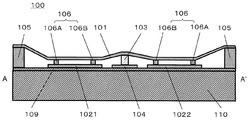
- the MEMS switch 100 shown in FIGS. 1 to 3 is a series type.
- an insulating layer 109 serving as an interlayer insulating film is provided on a substrate 110, and driving electrodes 1021 and 1022 and a signal electrode 104 serving as a second electrode serving as a signal transmission path are formed on the insulating layer 109.
- the movable electrode 101 is a deformable member and can also be called a movable part.
- the movable electrode 101 is provided with a contact electrode 103 that contacts the signal electrode 104 and a convex portion 106 (106A and 106B) that contacts the drive electrodes 1021 and 1022.
- the counter electrode that generates an electrostatic attractive force is divided between the movable electrode, which is the first electrode, to form drive electrodes 1021 and 1022 to which a voltage is applied. Accordingly, the drive electrodes 1021 and 1022 correspond to a third electrode and a fourth electrode, respectively. Since the drive electrode is not movable, it may be called a fixed electrode.
- the drive voltages V d1 and V d2 are not applied between the movable electrode 101 and the drive electrodes 1021, 1022.
- the movable electrode 101 is in an initial position that is not displaced, and the contact electrode 103 is not in contact with the signal electrode 104. Therefore, a signal conduction path is not formed between the signal electrode 104 on the input port side (IN) and the output port side (OUT). More specifically, since the electrostatic capacitance C c which is formed through the air gap between the signal electrode 104 and the contact electrode 103 becomes a small value, if the high-frequency signal propagates, the AC-impedance high state It becomes. For this reason, the power of the high frequency signal is greatly attenuated, and the high frequency signal cannot be propagated between the signal electrode 104 on the input port side and the output port side.
- the potential of the movable electrode 101 and the potential of the drive electrodes 1021, 1022 are made the same to eliminate the electrostatic force, and the movable electrode 101 returns to the initial position by its own spring force. In this way, the signal propagation path is opened and closed.
- FIG. 4 is a cross-sectional view of the vicinity of the contact when the MEMS switch of the present embodiment is in the ON state, showing the A-A ′ cross section in FIG.
- the convex portion 106 ⁇ / b> B provided on the movable electrode 101 is in contact with the floating island electrode 1026.
- the floating island electrode 1026 is a layer made of the same material as the drive electrodes 1021 and 1022 and having the same thickness, and is physically and electrically separated from the drive electrodes 1021 and 1022 by the slit 1020. Due to the presence of the floating island electrode 1026, the movable electrode 101 and the drive electrodes 1021 and 1022 do not have the same potential, and the electrostatic force can be maintained.
- the floating island electrode 1026 can be formed in the same layer as the drive electrodes 1021 and 1022 in one step, so that the manufacturing process can be simplified. It can be realized. Further, by forming the floating island electrode 1026, the convex portion 106 can be formed of the same material as that of the contact electrode 103, and in this respect also, the manufacturing process can be simplified.
- the spring constant of the movable electrode 101 after the contact is determined by a region bridged between the plurality of convex portions 106 and the contact electrode 103. Since the region becomes narrow, the spring constant is compared with the state of the initial position. growing.
- the arrangement of the convex portion 106 and the contact electrode 103 is set so that the spring force of the movable electrode 101 after the contact is greater than the electrostatic force so that the movable electrode 101 and the drive electrodes 1021 and 1022 do not contact with each other by the second pull-in after the contact. With such an arrangement, a gap is formed between the movable electrode 101 and the drive electrodes 1021 and 1022 after contact, and a point contact is made by the convex portion 106. This can avoid charging of the contact interface due to direct contact between the movable electrode 101 and the drive electrodes 1021 and 1022. Further, stiction between the movable electrode 101 and the drive electrodes 1021 and 1022 can be avoided.
- the height of the contact electrode 103 is set higher than the height of the gap so that the contact force due to the spring force acts even after the electrical contact point is formed. That is, when viewed from the substrate 110, the height (or thickness) of the contact electrode 103 is such that the position of the movable electrode 101 provided with the contact electrode is higher than the position of the movable electrode 101 provided with the convex portion. It is preferable to select the height (or thickness) of the convex portion 106. In general, since the thickness of the movable electrode 101 is constant, it is preferable that the height of the contact electrode 103 be larger than the height of the convex portion 106.
- the length l of the movable electrode 101 is the closest to the x coordinate of the side edge of the movable electrode 101 and the x coordinate of the side edge of the movable electrode 101 among the x coordinates of the side edges of the plurality of convex portions. Note that it refers to the difference between them (ie, the distance in the x direction).
- FIGS. 5 and 6 are cross-sectional views showing the A-A ′ section in FIG. 1, and illustrate the state when control signals are independently input to the two drive electrodes. A switching mechanism in the MEMS switch 100 will be described.
- control signals for applying drive voltages V d1 and V d2 between the movable electrode 101 and the drive electrodes 1021 and 1022 are sent to the drive electrodes 1021 and 1022, respectively.
- a control signal for applying a voltage to the drive electrode 1021 is sent, and a control signal for applying a voltage to the drive electrode 1022 is sent after a certain time.
- the movable electrode 101 is drawn to the drive electrode 1021 side, and the side of the contact electrode 103 close to the drive electrode 1021 first comes into contact with the signal electrode 104 and then the contact electrode.
- 103 slides on the signal electrode 104 toward the drive electrode 1021 (that is, in the direction indicated by the arrow in FIG. 5).
- the movable electrode 101 and the drive electrode 1021 do not come into contact with each other over a wide area, and only the convex portion 106 serves as the drive electrode (the floating island electrode 1026 in the illustrated form). In contact. That is, the contact area between the movable electrode 101 and the drive electrode 1021 is small, and therefore the frictional force generated between the movable electrode 101 and the drive electrode 1021 in the horizontal direction with the surface of the substrate 110 is small.
- the time difference for applying a voltage to the drive electrodes 1021 and 1022 is preferably about the same as the response time of the switch.
- the drive by the drive electrode 1021 is almost completed, and the movable electrode 101 is drawn to the drive electrode 1022 side from the state in which the movable electrode 101 is deformed asymmetrically. It can be smoothly slid on the electrode 104.
- the response time of the switch varies depending on the application of the device in which the switch is incorporated, and is generally several microseconds to several hundred microseconds. If the time difference is too small, the contact electrode 103 may not slide sufficiently. If the time difference is too large, it may be difficult to deform the movable electrode 101 in an asymmetrically deformed state (that is, from the state of FIG. 5 to the state of FIG. 6).
- the movable electrode 101 and the drive electrode 1022 are set to the same potential, and then the movable electrode 101 and the drive electrode 1021 are set to the same potential to eliminate the electrostatic force. As a result, the movable electrode 101 returns to the original initial position by its own spring force. Even when switching to the OFF state, by providing a time difference in the control signal applied to the two drive electrodes, the movable electrode 101 is restored asymmetrically, and the contact electrode 103 is slid on the signal electrode 104 while the contact electrode 103 is slid. 103 is separated from the signal electrode 104 to release the electrical contact.
- the movable electrode 101 has a doubly supported beam structure in which both ends are fixed.
- the movable electrode has a double-supported beam configuration, as shown in FIG. 5, the movable electrode 101 is reliably pulled to the right side after being pulled to the left side. Therefore, as shown in FIG. 5, the contact electrode 103 slides to the left and then to the right more reliably, and a high mechanical cleaning effect is obtained.
- the configuration of the present embodiment makes it possible to obtain a high contact force with an electrical contact, thereby reducing the physical contact area between the contact electrode 103 and the signal electrode 104 in the MEMS switch. This makes it possible to avoid a decrease in reliability due to stiction.
- the drive electrodes 1021 and 1022 are arranged so as to sandwich the contact electrode 103 therebetween. That is, the drive electrodes 1021 and 1022 are arranged on both sides of the contact electrode 103 when the direction parallel to the signal electrode 104 (vertical direction in the drawing) is the length direction and the direction orthogonal to the drive electrode 1021 and 1022 is the width direction.
- the drive electrodes 1021 and 1022 are arranged symmetrically with the signal electrode 104 and the contact electrode 103 connecting the signal electrode 104 as the center line. With such an arrangement, it is possible to apply a uniform contact force with no bias to the entire contact point between the contact electrode 103 and the signal electrode 104 in the ON state (the state shown in FIG. 6), and avoid contact force dispersion. can do.
- the convex portions 106 are arranged symmetrically with the signal electrode 104 and the contact electrode 103 connecting the same as the center line when viewed from above. Such an arrangement makes the gap formed on both sides of the contact electrode 103 symmetrical, and contributes to applying a uniform contact force with no bias to the electrical contacts on both sides of the contact electrode 103.
- the convex portion 106 may be disposed so as to be asymmetric as necessary, or may be disposed so as to face only one drive electrode.
- a plurality of convex portions 106 are provided and arranged at different positions so that the distances between the convex portions 106 and the electrical contacts are equal.
- convex portions 106 that are in contact with the drive electrodes 1021 and 1022 are provided, and each convex portion 106 is disposed on a circle centered on an electrical contact.
- the distance between the electrical contact and the convex portion refers to the distance between the center of the signal electrode 103 and the convex portion 106 when the electrical contact and the convex portion are in surface contact.
- the movable electrode 101 that is bridged in the region surrounded by the electrical contacts and the convex portions is supported not only in the x direction but also in the y direction, thereby increasing the spring force and allowing the movable electrode 101 to move. Pulling of the electrode 101 into the drive electrodes 1021 and 1022 can be avoided. Therefore, a gap between the movable electrode 101 and the drive electrodes 1021 and 1022 can be secured.
- the convex portion 106 When viewed from above, the convex portion 106 has an electrical contact (in the case of surface contact, the surface contact (signal electrode 103), as shown in the figure) and the convex portion (center of the convex portion).
- the area of the region formed by connecting them with a straight line is 20% or more of the area where the electrostatic force acts between the movable electrode 101 and the drive electrode 1021. It is preferable to provide. Thereby, a wide gap region formed by the movable electrode 101 bridging between the convex portion 106 and the contact electrode 103 and the drive electrodes 1021 and 1022 after the contact is secured.
- the spring force of the possible electrode 101 decreases, and the opposing area between the movable electrode 101 and the drive electrodes 1021 and 1022 in the gap region increases, increasing the electrostatic force. Thereby, it is possible to continue to apply electrostatic force to the contact even after contact.
- the area of the two drive electrodes is 1 mm 2
- the drive voltage is 7 V
- the thickness of the movable electrode is 8 ⁇ m
- the distance from the electrical contact to each projection can be set to a maximum of 0.3 mm.
- the total area of the regions surrounded by the electrical contacts and the protrusions is 0.23 mm 2 , which is 23% of the area where the electrostatic force acts between the movable electrode and the drive electrode.
- the number and position of the convex portions 106 are selected in consideration of the physical properties and dimensions of the movable electrode 101.
- the convex portion is preferably provided so as not to be positioned in the vicinity of the electrical contact and to be positioned in the peripheral edge portion of the drive electrodes 1021 and 1022. Thereby, the area of the region where the electrostatic force acts between the movable electrode 101 and the drive electrode 1021 can be increased.
- the convex portions 106 are arranged at substantially the apexes of the drive electrodes 1021 and 1022 that are substantially triangular when viewed from above, so that the region surrounded by the electrical contacts and the convex portions is as wide as possible. I have to. As a result, the gap region is widened and the capacitance is increased, thereby increasing the electrostatic force that is a force for maintaining the contact between the contact electrode 103 and the signal electrode 104 after the contact.
- the convex portion 106 is formed by selecting the number and position so that the movable electrode 101 and the drive electrodes 1021 and 1022 do not directly contact each other.
- contact force due to electrostatic force cannot be obtained.
- the movable electrode is greatly bent by adjusting the distance between the convex portion and the movable electrode and the distance between the convex portions. Is preferred.
- the electrostatic force F e is not obtained. In order to avoid this, it is preferable to determine the position and number of convex portions in consideration of the spring constant of the movable electrode 101 and the like.
- the MEMS switch 100 of this embodiment it is possible to provide a micro electromechanical switch that realizes highly reliable contact formation, which has been difficult to realize in the past, and an electric device using the same.
- This MEMS switch can be used for various electric devices, in particular, communication devices. Specifically, it can be used for a mobile phone, a transceiver unit of a wireless communication terminal, and an antenna device.
- the MEMS switch has a regular octagonal shape when viewed from above.
- the shape of the MEMS switch of the present invention is not limited to this, and may have other shapes such as a square, a regular hexagon, a circle, an ellipse, a rectangle, or a triangle.
- a switch (shunt type switch) having a configuration in which a contact portion of a movable electrode and a signal electrode to which signals are coupled in an equivalent circuit of a MEMS switch is connected in parallel to the transmission line and the tip is grounded. It is also applicable to.
- the position of the movable electrode in the ON state and the OFF state in the shunt type switch is opposite to those in the series type switch. In the OFF state, the movable electrode and the signal electrode are in contact with each other. The signal propagates to ground and not to the output port. At the ON time, the movable electrode and the signal electrode are not in contact with each other, and the signal propagates on the signal electrode from the input port toward the output port.
- the convex portion provided on the movable electrode side in the first embodiment may be provided on the drive electrode side.
- the convex portion may be made of an insulator. In that case, the movable electrode and the drive electrode can be prevented from having the same potential without providing the floating island electrode in the drive electrode.
- the movable electrode can be formed into a cantilever type or a cantilever type by etching using a sacrificial layer.
- the contact electrode is formed by forming a recess in the sacrificial layer by etching and depositing a contact electrode material (which may be the same as the material of the movable electrode) in the recess.
- the contact electrode 103 is preferably formed of a material such as platinum or ruthenium. Such materials are low resistance and have high stiffness, thus providing low contact resistance and highly reliable electrical contacts.
- the contact electrode 103 is preferably a rectangular parallelepiped, and preferably has a rectangular or square cross section. The contact electrode 103 having such a shape makes it possible to obtain a mechanical cleaning effect over a wide range because one side of the rectangular parallelepiped contacts the signal electrode 104 and slides on the signal electrode.
- a protrusion on the movable electrode When forming a protrusion on the movable electrode, masking and etching form a recess in the sacrificial layer that is different from the recess for forming the contact electrode, and deposits the material of the movable electrode in the recess and on the surface of the sacrificial layer. Then, the sacrificial layer is removed to form a movable electrode having a convex portion.
- the material of the convex portion may be a material (for example, an insulator) different from the material of the movable electrode.
- the insulating layer may be formed, for example, by thermally oxidizing the surface of a substrate made of silicon. The thickness of the insulating layer may be about 1 ⁇ m, for example.
- the driving electrode as the third electrode and the fourth electrode and the signal electrode as the second electrode are formed by depositing each electrode material on the insulating layer and patterning it by masking and etching.
- the thicknesses of the drive electrode as the third electrode and the fourth electrode and the thickness of the signal electrode as the second electrode may be about 0.5 to 1.0 ⁇ m.
- a control signal input circuit to the third electrode and the fourth electrode is provided independently, and the control signal to those electrodes is supplied.
- the inputs need to be made independently.
- a desired time difference can be provided in the input of control signals to the two electrodes.
- the potentials V d1 and V d2 of the two electrodes can be different from each other.
- V d1 When V d1 is applied and then V d2 is applied, the magnitude of V d2 is determined by the spring force of the first electrode (movable electrode 101) and the first electrode (movable electrode) when V d1 is applied. It is determined according to the distance of the gap between the electrode 101) and the fourth electrode (drive electrode 1022). In general, the spring force of the first electrode in a state where the V d1 is applied is greater than that of the state of V d1 is not applied, the deflecting it requires a greater electrostatic force. When V d1 is applied, the gap distance between the first electrode and the fourth electrode is smaller than that in the state where V d1 is not applied, and the first electrode is connected to the fourth electrode. The electrostatic force required to contact the electrodes is smaller.
- FIG. 9 is a cross-sectional view showing the configuration of the MEMS switch of the second embodiment.
- the top view of this MEMS switch is substantially the same as that of the first embodiment (that is, FIG. 1), and FIG. 9 shows the AA ′ cross section of FIG.
- an insulating layer 109 to be an interlayer insulating film 109 is provided on a substrate 110, two counter electrodes 1121 and 1122 and a signal electrode to be a signal transmission path on the insulating layer 109. 104 is provided.
- a doubly supported beam-type movable electrode 201 is provided so as to face these electrodes and be separated from these electrodes by bridging by two support portions 105.
- the movable electrode 201 includes two layers, and includes a cross-linked layer 201A cross-linked by a support portion, and drive electrode layers 2021 and 2022 that are layers to which a voltage is applied. These drive electrode layers 2021 and 2022 substantially divide the movable electrode, and a voltage can be applied to each drive electrode layer with a time difference.
- the movable electrode 201 is further provided with a contact electrode 103 in contact with the signal electrode 104 and provided with convex portions 106 (106A, 106B) in contact with the counter electrodes 1121 and 1122.
- Generation of electrostatic attractive force between the movable electrode 201 and the counter electrodes 1121 and 1122 is performed by applying a voltage to the drive electrode layers 2021 and 2022 of the movable electrode 201.
- the counter electrodes 1121 and 1122 are not movable and can be called fixed electrodes.
- the movable electrode 201 it is necessary to electrically insulate the bridging layer 201 from the drive electrode layers 2021 and 2022 with an insulator so that the voltage application to the drive electrode layers 2021 and 2022 is not affected by each other. There is. Or you may ensure the independence of two drive electrode layers by forming the bridge
- the drive electrode layers 2021 and 2022 are preferably formed to have substantially the same shape and dimensions as the counter electrodes 1121 and 1122 when viewed from above.
- the switching mechanism in the MEMS switch 200 is as described in connection with the first embodiment. Therefore, the detailed description is abbreviate
- FIG. 10 is a top view showing the configuration of the MEMS switch according to the third embodiment of the present invention.
- FIG. 11 shows a cross section taken along line AA ′ in FIG. 10, and is a cross-sectional view showing the configuration of the MEMS element in the OFF state.
- FIG. 12 is a cross-sectional view showing the configuration of the MEMS switch in the ON state, showing the AA ′ cross section in FIG.
- the MEMS switch 1000 shown in FIGS. 10 to 12 has the same configuration as the MEMS switch of Embodiment 1 except that it does not have a convex portion. Accordingly, the same members or elements are denoted by the same reference numerals. Even in the MEMS switch 1000 that does not include a convex portion, the switching signal ON / OFF operation can be executed by the same mechanism by implementing the control signal input method employed in the MEMS switch 100 of the first embodiment. That is, also in this embodiment, the contact electrode 103 can be slid on the signal electrode 104 by applying a voltage to the drive electrode 1022 after applying a voltage to the drive electrode 1021. Accordingly, a mechanical cleaning effect can be obtained, and stabilization of contact formation in repeated operations can be realized.
- a gap is secured between the movable electrode 101 and the drive electrodes 1021 and 1022 and an electrostatic force is applied to the movable electrode 101 and the drive electrodes 1021 and 1022 while the electrical contact is formed even in the form having no convex portion. . Therefore, it is necessary to design the movable electrode and the circuit and adjust the control signal so that the movable electrode 101 does not come into contact with the drive electrodes 1021 and 1022 by applying a voltage.
- the switch in which the movable electrode is a doubly supported beam type has been described.
- Embodiment 4 a mode in which the movable electrode is a cantilever type will be described.
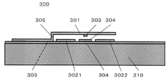
- an insulating layer 309 serving as an interlayer insulating film is provided over a substrate 310, and driving electrodes 3021 and 3022 and a signal electrode 304 serving as a signal transmission path are provided over the insulating layer 309. Is formed.
- a movable electrode 301 having a contact electrode 303 supported by a support portion 305 is provided so as to face these electrodes and be separated from these electrodes.
- the counter electrode facing the movable electrode is divided into two to form drive electrodes 3021 and 3022, and voltage is applied to these electrodes with a time difference.
- the movable electrode is not provided with a convex portion. Even when the movable electrode is a cantilever type, a convex portion may be provided as necessary.
- the switching mechanism in the MEMS switch 300 is as described in connection with the first embodiment. Specifically, after a voltage is applied to one of the drive electrodes 3021 and 3022, the voltage is preferably applied to the other with approximately the same time difference as the switch response time. Thereby, in a state where the contact electrode 303 is in contact with the signal electrode 304, the contact electrode 303 is later drawn and slid toward the drive electrode to which a voltage is applied, and a mechanical cleaning effect is obtained. As a result, the contact resistance can be lowered at the electrical contact. Also in this embodiment, since the movable electrode 301 is configured not to directly contact the drive electrodes 3021 and 3022, a high contact force is maintained by the electrostatic force generated between the movable electrode and the drive electrode. Can do.
- the MEMS switch according to the present invention has high reliability and is useful as a component of electrical equipment such as communication equipment.
- MEMS switch 101 100, 200, 300, 500, 1000 MEMS switch 101, 201, 301 Movable electrode 1020 Slit 1021, 1022, 3021, 3022 Drive electrode 1026 Floating island electrode 103, 303 Contact electrode 104, 304 Signal electrode 105, 305 Support section 106, 106A , 106B Protruding portion 109, 309 Insulating layer 110, 310 Substrate 201A Cross-linking layer 2021, 2022 Driving electrode layer 1121, 1122 Counter electrode 301, 501 Movable electrode 502 Driving electrode 503 Contact electrode 505 Supporting portion 509 Insulating layer
Landscapes
- Micromachines (AREA)
Abstract
Description
前記可動電極に対向し、かつ前記可動電極から離間して形成された信号電極と、
前記可動電極に対向し、かつ前記可動電極から離間して形成された対向電極とを有し、
前記可動電極と、対向電極との間に発生させた静電気力によって、前記可動電極と前記信号電極との間で電気的接点を形成し得る、MEMSスイッチであって、
前記可動電極と前記対向電極との間で静電気力を発生させるための電圧を、前記可動電極および前記対向電極のいずれか一方に印加するようになっており、
前記電圧が印加される電極が、複数に分割されており、
分割されたそれぞれの電極に電圧を印加することが時間差をもって行われる、
MEMSスイッチを提供する。
(実施の形態1)
図1は、本発明の実施の形態1におけるMEMSスイッチの構成を示す上面図であり、図2は、図1におけるA-A’断面を示しており、MEMS素子のOFF状態の構成を示す横断面図であり、図3は、図1におけるA-A’断面を示しており、MEMSスイッチのON状態の構成を示す横断面図である。
スイッチがOFFの状態においては、可動電極101と駆動電極1021、1022との間に駆動電圧Vd1およびVd2は印加しない。可動電極101は変位していない初期位置にあり、接触電極103は信号電極104と接触していない状態にある。したがって、入力ポート側(IN)と出力ポート側(OUT)の信号電極104の間には信号の導通経路は形成されない。より具体的には、信号電極104と接触電極103の間にエアーギャップを介して形成された静電容量Ccは小さい値となるので、高周波信号が伝播する場合、交流的にインピーダンスの高い状態となる。このため、高周波信号の電力は大きく減衰し、入力ポート側と出力ポート側の信号電極104の間を高周波信号が伝播できない状態となる。
本発明のさらに別の実施の形態においては、実施の形態1において可動電極側に設けられていた凸部を駆動電極側に設けてよい。
本発明のさらに別の実施の形態においては、凸部を絶縁体で構成してよい。その場合には、駆動電極内に浮き島電極を設けなくても、可動電極と駆動電極とが同電位となることを避けることができる。
実施の形態1では、対向電極が分割されて、第3および第4の電極として、駆動電極1021および1022を構成している形態を説明した。実施の形態2として、可動電極が2つに分割されて、分割された可動電極に、電圧の印加を時間差をもって行う形態を説明する。図9は、実施の形態2のMEMSスイッチの構成を示す横断面図である。このMEMSスイッチの上面図は、実施の形態1のそれと略同じ(即ち、図1)であり、図9は、図1のA-A’断面を示している。
実施の形態1および2は、可動電極に凸部を設けた形態である。しかし、このような凸部は必ずしも必要ではない。実施の形態3として、凸部を設けない形態を説明する。
図10は、本発明の実施の形態3におけるMEMSスイッチの構成を示す上面図である。図11は、図10におけるA-A’断面を示しており、MEMS素子のOFF状態の構成を示す横断面図である。図12は、図10におけるA-A’断面を示しており、MEMSスイッチのON状態の構成を示す横断面図である。
実施の形態1~3では、可動電極が両持ち梁型であるスイッチを説明した。実施の形態4として、可動電極が片持ち梁型である形態を説明する。図13に示すMEMSスイッチ300においては、基板310上に層間絶縁膜となる絶縁層309が設けられ、絶縁層309の上に、駆動電極3021および3022、ならびに信号の伝送路となる信号電極304が形成されている。これらの電極と対向し、これらの電極から離間するように、支持部305により支持された、接触電極303を有する可動電極301が設けられている。
101、201、301 可動電極
1020 スリット
1021、1022、3021、3022 駆動電極
1026 浮き島電極
103、303 接触電極
104、304 信号電極
105、305 支持部
106、106A、106B 凸部
109、309 絶縁層
110、310 基板
201A 架橋層
2021、2022 駆動電極層
1121、1122 対向電極
301、501 可動電極
502 駆動電極
503 接触電極
505 支持部
509 絶縁層
Claims (17)
- 可動電極と、
前記可動電極に対向し、かつ前記可動電極から離間して形成された信号電極と、
前記可動電極に対向し、かつ前記可動電極から離間して形成された対向電極とを有し、前記可動電極と、前記対向電極との間に発生させた静電気力によって、前記可動電極と前記信号電極との間で電気的接点を形成し得る、MEMSスイッチであって、
前記可動電極と前記対向電極との間で静電気力を発生させるための電圧を、前記可動電極および前記対向電極のいずれか一方に印加するようになっており、
前記電圧が印加される電極が、複数に分割されており、
分割されたそれぞれの電極に電圧を印加することが時間差をもって行われる、
MEMSスイッチ。 - 前記時間差が、スイッチの応答時間と略同じである、請求項1に記載のMEMSスイッチ。
- 前記複数に分割された電極が、前記電気的接点に対して対称となるように配置されている、請求項1または2に記載のMEMSスイッチ。
- 前記可動電極を第1の電極、前記信号電極を第2の電極とした場合に、前記対向電極が2つに分割されて、第3の電極と第4の電極を形成している、請求項1~3のいずれか1項に記載のMEMSスイッチ。
- 前記第1の電極と前記第3の電極および/または前記第4の電極との間で接点を形成し得る凸部が、前記第1の電極、前記第3の電極および前記第4の電極から選択される一または複数の電極に設けられており、
前記第1の電極と前記第2の電極との間で電気的接点が形成されたときに、前記第1の電極と、前記第3の電極および/または前記第4の電極との間にギャップが形成される、請求項4に記載のMEMSスイッチ。 - 前記凸部の数および位置が、前記電気的接点が形成されているときに、前記第1の電極と、前記第3の電極および/または前記第4の電極とが直接接触しないように、選択されている、請求項5に記載のMEMSスイッチ。
- 前記凸部が複数個設けられており、前記複数個の凸部が、前記電気的接点から延びる複数の放射線上にそれぞれ1つずつ設けられている、請求項5または6に記載のMEMSスイッチ。
- 前記複数の凸部が、各凸部と前記電気的接点との距離が等しくなり、かつ前記複数の凸部の位置が互いに異なるように、配置されている、請求項7に記載のMEMSスイッチ。
- 前記凸部が、前記第1の電極と前記第3の電極との間で複数個設けられており、前記凸部の数および位置が、前記電気的接点と前記凸部とによって囲まれる領域の面積が、前記第1の電極と前記第3の電極との間で静電気力が作用する面積の20%以上となるように、選択されている、請求項5~8のいずれか1項に記載のMEMSスイッチ。
- 前記凸部が、前記第1の電極と前記第4の電極との間で複数個設けられており、前記凸部の数および位置が、前記電気的接点と前記凸部とによって囲まれる領域が、前記第1の電極と前記第4の電極との間で静電気力が作用する面積の20%以上となるように、選択されている、請求項5~9のいずれか1項に記載のMEMSスイッチ。
- 前記凸部が、前記第3の電極および/または前記第4の電極内に形成された浮き島電極と接点を形成し得る、請求項5~10のいずれか1項に記載のMEMSスイッチ。
- 前記凸部が、絶縁体である、請求項5~11のいずれか1項に記載のMEMSスイッチ。
- 前記電気的接点における前記第1の電極が、前記凸部における前記第1の電極よりも高い位置にある、請求項5~12のいずれか1項に記載のMEMSスイッチ。
- 前記電気的接点において、前記第1の電極に接触電極が形成され、接触電極の高さが、前記凸部の高さよりも大きい、請求項13に記載のMEMSスイッチ。
- 前記第3の電極および前記第4の電極が、上から見たときに前記電気的接点を挟むように配置されている、請求項4~14のいずれか1項に記載のMEMSスイッチ。
- 前記可動電極が両持ち梁である、請求項1~15のいずれか1項に記載のMEMSスイッチ。
- 請求項1~16のいずれか1項に記載のMEMSスイッチを有する通信用機器。
Priority Applications (2)
| Application Number | Priority Date | Filing Date | Title |
|---|---|---|---|
| JP2011531776A JP4887466B2 (ja) | 2009-09-17 | 2010-08-26 | Memsスイッチおよびそれを用いた通信装置 |
| US13/262,666 US8847087B2 (en) | 2009-09-17 | 2010-08-26 | MEMS switch and communication device using the same |
Applications Claiming Priority (2)
| Application Number | Priority Date | Filing Date | Title |
|---|---|---|---|
| JP2009-215844 | 2009-09-17 | ||
| JP2009215844 | 2009-09-17 |
Publications (1)
| Publication Number | Publication Date |
|---|---|
| WO2011033729A1 true WO2011033729A1 (ja) | 2011-03-24 |
Family
ID=43758344
Family Applications (1)
| Application Number | Title | Priority Date | Filing Date |
|---|---|---|---|
| PCT/JP2010/005269 Ceased WO2011033729A1 (ja) | 2009-09-17 | 2010-08-26 | Memsスイッチおよびそれを用いた通信装置 |
Country Status (3)
| Country | Link |
|---|---|
| US (1) | US8847087B2 (ja) |
| JP (1) | JP4887466B2 (ja) |
| WO (1) | WO2011033729A1 (ja) |
Cited By (1)
| Publication number | Priority date | Publication date | Assignee | Title |
|---|---|---|---|---|
| CN106477515A (zh) * | 2015-09-01 | 2017-03-08 | 阿自倍尔株式会社 | 微细机械装置及其制造方法 |
Families Citing this family (9)
| Publication number | Priority date | Publication date | Assignee | Title |
|---|---|---|---|---|
| FR2964243A1 (fr) * | 2010-08-27 | 2012-03-02 | Commissariat Energie Atomique | Dispositif a contact intermittent ameliore par dielectrophorese |
| US9320481B2 (en) | 2014-03-31 | 2016-04-26 | General Electric Company | Systems and methods for X-ray imaging |
| US9748048B2 (en) * | 2014-04-25 | 2017-08-29 | Analog Devices Global | MEMS switch |
| CN107077971A (zh) * | 2014-10-03 | 2017-08-18 | 维斯普瑞公司 | 减少微机电系统装置中的介电充电的系统、装置和方法 |
| FR3027448B1 (fr) * | 2014-10-21 | 2016-10-28 | Airmems | Commutateur microelectromecanique robuste |
| WO2018063814A1 (en) * | 2016-09-29 | 2018-04-05 | Cavendish Kinetics, Inc | Mems rf-switch with near-zero impact landing |
| WO2021070660A1 (ja) * | 2019-10-10 | 2021-04-15 | パナソニックIpマネジメント株式会社 | 入力装置 |
| KR102509983B1 (ko) * | 2020-07-16 | 2023-03-14 | 삼성전자주식회사 | 전열 구동 기계식 스위치 소자 및 이를 이용한 메모리 장치 |
| DE102024207606A1 (de) * | 2024-08-09 | 2026-02-12 | Robert Bosch Gesellschaft mit beschränkter Haftung | Mikromechanischer Schalter |
Citations (3)
| Publication number | Priority date | Publication date | Assignee | Title |
|---|---|---|---|---|
| JP2003136496A (ja) * | 2001-11-06 | 2003-05-14 | Omron Corp | 静電アクチュエータ及び該アクチュエータを用いた静電マイクロリレーその他の機器 |
| JP2006269127A (ja) * | 2005-03-22 | 2006-10-05 | Toshiba Corp | マイクロマシンスイッチ及び電子機器 |
| JP2008311225A (ja) * | 2007-05-17 | 2008-12-25 | Panasonic Corp | 電気機械素子、その駆動方法およびそれを用いた電気機器 |
Family Cites Families (10)
| Publication number | Priority date | Publication date | Assignee | Title |
|---|---|---|---|---|
| US6115231A (en) * | 1997-11-25 | 2000-09-05 | Tdk Corporation | Electrostatic relay |
| US6046659A (en) * | 1998-05-15 | 2000-04-04 | Hughes Electronics Corporation | Design and fabrication of broadband surface-micromachined micro-electro-mechanical switches for microwave and millimeter-wave applications |
| KR100506583B1 (ko) | 2000-04-21 | 2005-08-08 | 오므론 가부시키가이샤 | 정전형 릴레이 및 해당 릴레이를 이용한 통신용 기기 |
| US6787438B1 (en) * | 2001-10-16 | 2004-09-07 | Teravieta Technologies, Inc. | Device having one or more contact structures interposed between a pair of electrodes |
| US6608268B1 (en) * | 2002-02-05 | 2003-08-19 | Memtronics, A Division Of Cogent Solutions, Inc. | Proximity micro-electro-mechanical system |
| US7551048B2 (en) | 2002-08-08 | 2009-06-23 | Fujitsu Component Limited | Micro-relay and method of fabricating the same |
| US7106066B2 (en) * | 2002-08-28 | 2006-09-12 | Teravicta Technologies, Inc. | Micro-electromechanical switch performance enhancement |
| US20050062565A1 (en) * | 2003-09-18 | 2005-03-24 | Chia-Shing Chou | Method of using a metal platform for making a highly reliable and reproducible metal contact micro-relay MEMS switch |
| US7101724B2 (en) * | 2004-02-20 | 2006-09-05 | Wireless Mems, Inc. | Method of fabricating semiconductor devices employing at least one modulation doped quantum well structure and one or more etch stop layers for accurate contact formation |
| US7362199B2 (en) * | 2004-03-31 | 2008-04-22 | Intel Corporation | Collapsible contact switch |
-
2010
- 2010-08-26 US US13/262,666 patent/US8847087B2/en active Active
- 2010-08-26 WO PCT/JP2010/005269 patent/WO2011033729A1/ja not_active Ceased
- 2010-08-26 JP JP2011531776A patent/JP4887466B2/ja active Active
Patent Citations (3)
| Publication number | Priority date | Publication date | Assignee | Title |
|---|---|---|---|---|
| JP2003136496A (ja) * | 2001-11-06 | 2003-05-14 | Omron Corp | 静電アクチュエータ及び該アクチュエータを用いた静電マイクロリレーその他の機器 |
| JP2006269127A (ja) * | 2005-03-22 | 2006-10-05 | Toshiba Corp | マイクロマシンスイッチ及び電子機器 |
| JP2008311225A (ja) * | 2007-05-17 | 2008-12-25 | Panasonic Corp | 電気機械素子、その駆動方法およびそれを用いた電気機器 |
Cited By (1)
| Publication number | Priority date | Publication date | Assignee | Title |
|---|---|---|---|---|
| CN106477515A (zh) * | 2015-09-01 | 2017-03-08 | 阿自倍尔株式会社 | 微细机械装置及其制造方法 |
Also Published As
| Publication number | Publication date |
|---|---|
| JPWO2011033729A1 (ja) | 2013-02-07 |
| US20120031744A1 (en) | 2012-02-09 |
| US8847087B2 (en) | 2014-09-30 |
| JP4887466B2 (ja) | 2012-02-29 |
Similar Documents
| Publication | Publication Date | Title |
|---|---|---|
| JP4887466B2 (ja) | Memsスイッチおよびそれを用いた通信装置 | |
| JP2008311225A (ja) | 電気機械素子、その駆動方法およびそれを用いた電気機器 | |
| TWI466374B (zh) | 電子元件、可變電容、微開關、微開關的驅動方法、以及mems型電子元件 | |
| JP4186727B2 (ja) | スイッチ | |
| KR100492004B1 (ko) | 미세전자기계적 시스템 기술을 이용한 고주파 소자 | |
| JP2001179699A (ja) | 二重マイクロ−電子機械アクチュエータ装置 | |
| EP2200063B1 (en) | Micro-electromechanical system switch | |
| US8207460B2 (en) | Electrostatically actuated non-latching and latching RF-MEMS switch | |
| JP4887465B2 (ja) | Memsスイッチおよびそれを用いた通信装置 | |
| JP2006147540A (ja) | 電気機械スイッチ | |
| KR20100074027A (ko) | 마이크로 전자기계 시스템 스위치 | |
| KR101030549B1 (ko) | 마이크로전자기계시스템을 이용한 알에프 스위치 | |
| JP2009021227A (ja) | 電気機械スイッチ、それを用いたフィルタ、および通信機器 | |
| JP2009016161A (ja) | スイッチ及びこれを用いた無線端末 | |
| JP5130291B2 (ja) | 電気機械素子およびそれを用いた電気機器 | |
| US20070116406A1 (en) | Switch | |
| CN107004541A (zh) | 具有直插式mems开关的多通道继电器组合件 | |
| US7109560B2 (en) | Micro-electromechanical system and method for production thereof | |
| KR100520891B1 (ko) | 잔류응력 및 압전구동력을 이용한 초소형 전기 기계시스템 고주파 스위치 | |
| JP5483574B2 (ja) | Memsスイッチ | |
| KR20040111354A (ko) | 마이크로-전자기계 시스템을 갖춘 마이크로스위치 | |
| KR20060070957A (ko) | 정전기력 구동 rf mems 스위치 및 그 제조 방법 | |
| JP2008300301A (ja) | マイクロスイッチ及びその駆動方法 |
Legal Events
| Date | Code | Title | Description |
|---|---|---|---|
| 121 | Ep: the epo has been informed by wipo that ep was designated in this application |
Ref document number: 10816844 Country of ref document: EP Kind code of ref document: A1 |
|
| WWE | Wipo information: entry into national phase |
Ref document number: 2011531776 Country of ref document: JP |
|
| WWE | Wipo information: entry into national phase |
Ref document number: 13262666 Country of ref document: US |
|
| NENP | Non-entry into the national phase |
Ref country code: DE |
|
| 122 | Ep: pct application non-entry in european phase |
Ref document number: 10816844 Country of ref document: EP Kind code of ref document: A1 |