WO2011021244A1 - 半導体装置の製造方法 - Google Patents
半導体装置の製造方法 Download PDFInfo
- Publication number
- WO2011021244A1 WO2011021244A1 PCT/JP2009/003993 JP2009003993W WO2011021244A1 WO 2011021244 A1 WO2011021244 A1 WO 2011021244A1 JP 2009003993 W JP2009003993 W JP 2009003993W WO 2011021244 A1 WO2011021244 A1 WO 2011021244A1
- Authority
- WO
- WIPO (PCT)
- Prior art keywords
- insulating film
- film
- forming
- opening
- wiring
- Prior art date
- Legal status (The legal status is an assumption and is not a legal conclusion. Google has not performed a legal analysis and makes no representation as to the accuracy of the status listed.)
- Ceased
Links
Images












Classifications
-
- H—ELECTRICITY
- H10—SEMICONDUCTOR DEVICES; ELECTRIC SOLID-STATE DEVICES NOT OTHERWISE PROVIDED FOR
- H10W—GENERIC PACKAGES, INTERCONNECTIONS, CONNECTORS OR OTHER CONSTRUCTIONAL DETAILS OF DEVICES COVERED BY CLASS H10
- H10W20/00—Interconnections in chips, wafers or substrates
- H10W20/40—Interconnections external to wafers or substrates, e.g. back-end-of-line [BEOL] metallisations or vias connecting to gate electrodes
- H10W20/45—Interconnections external to wafers or substrates, e.g. back-end-of-line [BEOL] metallisations or vias connecting to gate electrodes characterised by their insulating parts
- H10W20/47—Interconnections external to wafers or substrates, e.g. back-end-of-line [BEOL] metallisations or vias connecting to gate electrodes characterised by their insulating parts comprising two or more dielectric layers having different properties, e.g. different dielectric constants
-
- H—ELECTRICITY
- H10—SEMICONDUCTOR DEVICES; ELECTRIC SOLID-STATE DEVICES NOT OTHERWISE PROVIDED FOR
- H10W—GENERIC PACKAGES, INTERCONNECTIONS, CONNECTORS OR OTHER CONSTRUCTIONAL DETAILS OF DEVICES COVERED BY CLASS H10
- H10W20/00—Interconnections in chips, wafers or substrates
- H10W20/01—Manufacture or treatment
- H10W20/071—Manufacture or treatment of dielectric parts thereof
- H10W20/072—Manufacture or treatment of dielectric parts thereof of dielectric parts comprising air gaps
-
- H—ELECTRICITY
- H10—SEMICONDUCTOR DEVICES; ELECTRIC SOLID-STATE DEVICES NOT OTHERWISE PROVIDED FOR
- H10W—GENERIC PACKAGES, INTERCONNECTIONS, CONNECTORS OR OTHER CONSTRUCTIONAL DETAILS OF DEVICES COVERED BY CLASS H10
- H10W20/00—Interconnections in chips, wafers or substrates
- H10W20/01—Manufacture or treatment
- H10W20/071—Manufacture or treatment of dielectric parts thereof
- H10W20/074—Manufacture or treatment of dielectric parts thereof of dielectric parts comprising thin functional dielectric layers, e.g. dielectric etch-stop, barrier, capping or liner layers
- H10W20/076—Manufacture or treatment of dielectric parts thereof of dielectric parts comprising thin functional dielectric layers, e.g. dielectric etch-stop, barrier, capping or liner layers in via holes or trenches
-
- H—ELECTRICITY
- H10—SEMICONDUCTOR DEVICES; ELECTRIC SOLID-STATE DEVICES NOT OTHERWISE PROVIDED FOR
- H10W—GENERIC PACKAGES, INTERCONNECTIONS, CONNECTORS OR OTHER CONSTRUCTIONAL DETAILS OF DEVICES COVERED BY CLASS H10
- H10W20/00—Interconnections in chips, wafers or substrates
- H10W20/01—Manufacture or treatment
- H10W20/071—Manufacture or treatment of dielectric parts thereof
- H10W20/081—Manufacture or treatment of dielectric parts thereof by forming openings in the dielectric parts
- H10W20/084—Manufacture or treatment of dielectric parts thereof by forming openings in the dielectric parts for dual-damascene structures
- H10W20/085—Manufacture or treatment of dielectric parts thereof by forming openings in the dielectric parts for dual-damascene structures involving intermediate temporary filling with material
-
- H—ELECTRICITY
- H10—SEMICONDUCTOR DEVICES; ELECTRIC SOLID-STATE DEVICES NOT OTHERWISE PROVIDED FOR
- H10W—GENERIC PACKAGES, INTERCONNECTIONS, CONNECTORS OR OTHER CONSTRUCTIONAL DETAILS OF DEVICES COVERED BY CLASS H10
- H10W20/00—Interconnections in chips, wafers or substrates
- H10W20/01—Manufacture or treatment
- H10W20/071—Manufacture or treatment of dielectric parts thereof
- H10W20/081—Manufacture or treatment of dielectric parts thereof by forming openings in the dielectric parts
- H10W20/089—Manufacture or treatment of dielectric parts thereof by forming openings in the dielectric parts using processes for implementing desired shapes or dispositions of the openings, e.g. double patterning
-
- H—ELECTRICITY
- H10—SEMICONDUCTOR DEVICES; ELECTRIC SOLID-STATE DEVICES NOT OTHERWISE PROVIDED FOR
- H10W—GENERIC PACKAGES, INTERCONNECTIONS, CONNECTORS OR OTHER CONSTRUCTIONAL DETAILS OF DEVICES COVERED BY CLASS H10
- H10W20/00—Interconnections in chips, wafers or substrates
- H10W20/40—Interconnections external to wafers or substrates, e.g. back-end-of-line [BEOL] metallisations or vias connecting to gate electrodes
- H10W20/41—Interconnections external to wafers or substrates, e.g. back-end-of-line [BEOL] metallisations or vias connecting to gate electrodes characterised by their conductive parts
- H10W20/42—Vias, e.g. via plugs
-
- H—ELECTRICITY
- H10—SEMICONDUCTOR DEVICES; ELECTRIC SOLID-STATE DEVICES NOT OTHERWISE PROVIDED FOR
- H10W—GENERIC PACKAGES, INTERCONNECTIONS, CONNECTORS OR OTHER CONSTRUCTIONAL DETAILS OF DEVICES COVERED BY CLASS H10
- H10W20/00—Interconnections in chips, wafers or substrates
- H10W20/40—Interconnections external to wafers or substrates, e.g. back-end-of-line [BEOL] metallisations or vias connecting to gate electrodes
- H10W20/45—Interconnections external to wafers or substrates, e.g. back-end-of-line [BEOL] metallisations or vias connecting to gate electrodes characterised by their insulating parts
- H10W20/46—Interconnections external to wafers or substrates, e.g. back-end-of-line [BEOL] metallisations or vias connecting to gate electrodes characterised by their insulating parts comprising air gaps
Definitions
- the present invention relates to a method for manufacturing a semiconductor device.
- the low dielectric constant material include a material having a dielectric constant lower than that of silicon oxide, such as silicon carbide oxide and silicon carbide.
- the wiring pitch becomes narrower, and further reduction of inter-wiring parasitic capacitance is required.
- a structure in which a cavity called a space or an air gap is formed around the wiring is known.
- the method for forming a space around the wiring includes, for example, the following steps.
- an Si 3 N 4 film is formed on each of the upper and side surfaces of the wiring, and further, an SiO 2 interlayer insulating film that covers the Si 3 N 4 film is formed. Subsequently, an opening exposing a part of the Si 3 N 4 film is formed on the wiring in the interlayer insulating film. Further, a barrier metal is formed on the inner peripheral surface of the opening. Thereafter, the Si 3 N 4 film is removed by wet etching through the opening, thereby forming a space between the wiring and the interlayer insulating film. After forming the space, a tungsten film is formed to a depth reaching the wiring from the inside of the opening, and this is used as a plug.
- the following methods are known for forming an air gap around the wiring.
- a groove is formed in the SiOC film, and then a damage layer is formed on the sidewall of the groove of the SiOC film, and then a thin dielectric layer is formed on and in the SiOC film, and the dielectric thin film is side-etched by etch back. Leave beside the damage layer as a wall protection layer.
- an air gap is formed on the side of the copper wiring by selectively etching the damaged layer using hydrofluoric acid. After that, the air gap, the SiOC film, and the copper wiring are capped with a dielectric film.
- a deep gap is formed by etching an insulating film between a plurality of wirings in the same layer. Thereafter, an SiOC film is formed on the wiring under conditions with a pinch-off effect. According to the pinch-off effect, an air gap is formed between the wirings.
- a semiconductor device manufacturing method capable of forming a cavity well around a damascene or dual damascene wiring structure.
- a step of forming a first insulating film above a semiconductor substrate, and a step of forming a second insulating film on the first insulating film having a different etching characteristic from the first insulating film A step of forming an opening in the first insulating film and the second insulating film, a step of etching the first insulating film from the inside of the opening to widen the opening and forming a cavity, A semiconductor device comprising: forming a third insulating film in the opening while leaving the cavity; and forming a conductive film in the opening after forming the third insulating film.
- the first insulating film is etched to widen the opening area under the opening portion in the lateral direction to form a cavity. is doing. Thereafter, the cavity is covered with the third insulating film from the inside of the opening, and then the conductive film is formed in the opening, whereby the cavity can be formed around the conductive film.
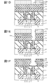
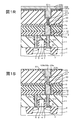
- 1A to 1C are cross-sectional views (parts 1 to 3) showing a process for forming a semiconductor device according to the first embodiment of the present invention.
- 1D to 1F are cross-sectional views (parts 4 to 6) showing a process for forming a semiconductor device according to the first embodiment of the invention.
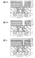
- 1G to 1I are cross-sectional views (Nos. 7 to 9) showing the process for forming the semiconductor device according to the first embodiment of the invention.
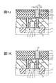
- 1J and 1K are cross-sectional views (Nos. 10 and 11) showing a process for forming a semiconductor device according to the first embodiment of the invention.
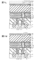
- 1L and 1M are cross-sectional views (Nos. 12 and 13) showing the process of forming the semiconductor device according to the first embodiment of the invention.
- FIG. 1N and FIG. 1O are cross-sectional views (Nos. 14 and 15) showing a process for forming a semiconductor device according to the first embodiment of the present invention.
- FIGS. 1p and 1Q are cross-sectional views (Nos. 16 and 17) showing the process of forming the semiconductor device according to the first embodiment of the invention.
- 1R and FIG. 1S are cross-sectional views (Nos. 18 and 19) showing a process for forming a semiconductor device according to the first embodiment of the present invention.
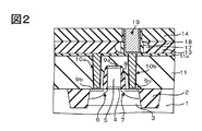
- FIG. 2 is a cross-sectional view showing another example of the process of forming the semiconductor device according to the first embodiment of the present invention.
- FIG. 3 is a cross-sectional view showing still another example of the process of forming the semiconductor device according to the first embodiment of the present invention.
- 4A and 4B are cross-sectional views showing another example of a method for covering the opening of the air gap in the process of forming the semiconductor device according to the first embodiment of the present invention.
- 5A and 5B are cross-sectional views showing still another example of a method of covering the opening of the air gap in the process of forming the semiconductor device according to the first embodiment of the present invention.
- 6A to 6E are cross-sectional views illustrating the steps of forming a semiconductor device according to the second embodiment of the present invention.
- 7A to 7D are cross-sectional views (parts 1 to 4) showing a process for forming a semiconductor device according to the third embodiment of the invention.
- 7E to 7H are cross-sectional views (Nos.
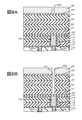
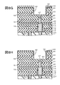
- FIGS. 8I and 8J are cross-sectional views (Nos. 1 and 2) showing a process for forming a semiconductor device according to the fourth embodiment of the invention.
- 8C and 8D are cross-sectional views (Nos. 3 and 4) showing the process of forming the semiconductor device according to the fourth embodiment of the invention.
- 8E and 8F are cross-sectional views (Nos. 5 and 6) showing the process for forming the semiconductor device according to the fourth embodiment of the invention.
- 8G and 8H are cross-sectional views (Nos. 7 and 8) showing the process of forming the semiconductor device according to the fourth embodiment of the invention.
- FIGS. 8I and 8J are cross-sectional views (Nos.
- FIG. 9 and 10 showing the step of forming the semiconductor device according to the fourth embodiment of the invention.
- FIG. 8K is a sectional view (No. 11) showing the process for forming the semiconductor device according to the fourth embodiment of the invention.
- 9A and 9B are cross-sectional views showing another example of a method for covering the opening of the air gap in the process of forming the semiconductor device according to the fourth embodiment of the present invention.
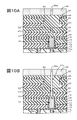
- 10A and 10B are cross-sectional views (Nos. 1 and 2) showing another example of a method for forming an air gap in the step of forming a semiconductor device according to the fourth embodiment of the present invention.
- 10C and 10D are cross-sectional views (Nos.
- FIG. 3 and 4 show another example of the method of forming the air gap in the process of forming the semiconductor device according to the fourth embodiment of the present invention.
- 10E and 10F are cross-sectional views (Nos. 5 and 6) showing another example of a method for forming an air gap in the process of forming a semiconductor device according to the fourth embodiment of the present invention.
- FIG. 11 is a cross-sectional view showing another method of forming wirings and vias in the process of forming a semiconductor device according to the fourth embodiment of the present invention.
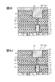
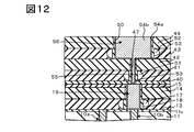
- FIG. 12 is a cross-sectional view showing still another method for forming wirings and vias in the process of forming a semiconductor device according to the fourth embodiment of the present invention.
- 13A and 13B are cross-sectional views showing another method of forming an air gap in the process of forming a semiconductor device according to the fourth embodiment of the present invention.
- an element isolation structure is formed on a semiconductor substrate, for example, an n-type or p-type silicon substrate 1.
- the semiconductor substrate may be an SOI substrate.
- As an element isolation structure for example, shallow trench isolation (STI) 2 is formed around the active region.
- STI2 is formed by the following method.
- a silicon oxide film and a silicon nitride film are sequentially formed on the silicon substrate 1, and then the silicon nitride film and the silicon oxide film are patterned by photolithography to form an opening in the element isolation region. Thereafter, the silicon substrate 1 is etched through the opening to form a groove in the element isolation region.
- the insulating film on the silicon nitride film is removed by a chemical mechanical polishing (CMP) method, and the insulating film remaining in the trench is defined as STI2.
- CMP chemical mechanical polishing
- a silicon oxide film is formed as the insulating film in the trench.
- the silicon nitride film and the silicon oxide film are removed from the upper surface of the silicon substrate 1.
- a silicon oxide film may be formed on the surface of the silicon substrate 1 by the LOCOS method instead of the STI 2.
- p-type impurities such as boron are ion-implanted into the NMOS formation region partitioned by the STI 2 to form the p-well 3.
- impurity ions are implanted, a region where ions are not implanted is covered with a resist pattern.
- n-type impurities are ion-implanted into a PMOS formation region (not shown) of the silicon substrate 1 to form an n-well.
- an NMOS transistor and a multilayer wiring structure thereon are mainly described.
- a silicon oxide film as a gate insulating film 4 is formed on the surface of the silicon substrate 1 to a thickness of about 1.5 nm, for example, by a dry thermal oxidation method.
- a polysilicon film is formed on the gate insulating film 4 and the STI 2 by a CVD method to a thickness of, for example, about 100 nm.
- phosphorus which is an n-type impurity, is ion-implanted into a region above the p-well 3 in the polysilicon film.
- annealing for example, rapid thermal annealing (RTA).
- the polysilicon film is patterned by photolithography to leave the polysilicon film as the gate electrode 5 above the p-well 3.
- the width of the gate electrode 5, that is, the gate length is, for example, about 32 nm.
- n-type impurity such as phosphorus or arsenic is ion-implanted into the p-well 3 using the gate electrode 5, STI2, etc. as a mask.
- n-type extension regions 6 a and 7 a are formed in the silicon substrate 1 on both sides of the gate electrode 5.
- a silicon oxide film is formed by, for example, a CVD method.
- n-type impurities are ion-implanted into the p-well 3 using the gate electrode 5 and the sidewalls 8 as masks, whereby a high-concentration n-type impurity region 6b is formed in the silicon substrate 1 on both sides of the gate electrode 5. , 7b.
- n-type extension regions 6a and 7a and the high-concentration n-type impurity regions 6b and 7b are activated by, for example, the RTA method.
- the n-type extension regions 6a and 7a and the high-concentration n-type impurity regions 6b and 7b that overlap in the regions on both sides of the gate electrode 5 become the source / drain regions 6 and 7, respectively.
- the regions not subjected to ion implantation are covered with a photoresist.
- a metal film covering the gate electrode 5 and the source / drain regions 6 and 7, for example, a nickel film which is a refractory metal is formed on the silicon substrate 1.
- a nickel film which is a refractory metal is formed on the silicon substrate 1.
- silicide layers 9a, 9b and 9c are formed on the gate electrode 5 and the source / drain regions 6 and 7, respectively.
- the nickel film is removed.
- an insulating film such as a silicon nitride film is formed on the silicon substrate 1 in a region where the silicide layer is not formed before the metal film is formed.
- the silicon nitride film is removed by, for example, hot phosphoric acid after the silicide layers 9a, 9b, and 9c are formed.
- the basic structure of the N-type MOS transistor T is formed in the NMOS formation region by the p well 3, the gate insulating film 4, the gate electrode 5, the source / drain regions 6, 7, and the like.
- a first interlayer insulating film 11 is formed on the N-type MOS transistor T and the silicon substrate 1.
- a PSG film is formed as the first interlayer insulating film 11 by the CVD method. Further, the upper surface of the first interlayer insulating film 11 is planarized by the CMP method. Thereafter, a first cap insulating film 11u is formed on the first interlayer insulating film 11 to a thickness of, for example, about 30 nm by plasma CVD.
- the material of the first cap insulating film 11u is selected from silicon carbide (SiC), silicon carbonitride (SiON), boron nitride (BN), or the like, or any of those materials containing hydrogen.
- a resist pattern (not shown) having an opening above the source / drain regions 6 and 7 is formed on the first cap insulating film 11u. Further, the first cap insulating film 11u and the first interlayer insulating film 11 are etched by, for example, the RIE method through the opening of the resist pattern, thereby forming contact holes 11a and 11b on the source / drain regions 6 and 7, respectively.
- a base metal film 12a of a titanium layer or a titanium nitride layer is formed on the inner surfaces of the contact holes 11a and 11b by, for example, a sputtering method, and then a tungsten film 12b is formed in the contact hole 11a by a CVD method.
- the tungsten film 12b is formed to a thickness that completely fills the contact hole 11a.
- the tungsten film 12b and the base metal film 12a formed on the first cap insulating film 11u are removed by the CMP method.
- the tungsten film 12b and the base metal film 12a left in the contact holes 11a and 11b are used as the conductive plugs 10a and 10b.
- Each of the conductive plugs 10a and 10b above the p-well 3 is connected to the source / drain regions 6 and 7 on both sides of the gate electrode 5 through silicide layers 9b and 9c. Note that a conductive plug is also connected to the gate electrode 5 through a silicide layer 9a in a region not shown.
- a second interlayer insulating film 13, a third interlayer insulating film 14, and a second cap insulating film 15 are sequentially formed on the first cap insulating film 11u.
- the total thickness of the second and third interlayer insulating films 13 and 14 is adjusted to be, for example, 50 nm to 200 nm.
- the respective materials of the second interlayer insulating film 13 and the third interlayer insulating film 14 are silicon oxide (SiO), silicon carbide oxide (SiOC), silicon oxyfluoride (SiOF), boron nitride (BN), or the like. These materials are selected from materials containing hydrogen.
- the material of the second cap insulating film 15 is selected from SiC, SiON, BN, or the like, or any of those materials containing hydrogen.
- the material is selected on the condition that the second interlayer insulating film 13 can be selectively etched with respect to the third interlayer insulating film 14 and the first and second cap insulating films 11u and 15.
- the second interlayer insulating film 13 is formed of a material that can increase the etching rate with respect to the third interlayer insulating film 14.
- the second interlayer insulating film 13 may have a lower dielectric constant than the third interlayer insulating film 14.
- an SiO film is formed as the second interlayer insulating film 13 to a thickness of 5 nm to 100 nm by plasma CVD.
- a SiC film or a SiOC film is formed to a thickness of 5 nm to 100 nm by plasma CVD.
- an SiC film is formed to a thickness of 15 nm to 60 nm by plasma CVD.
- the second interlayer insulating film 13 and the third interlayer insulating film 14 use the same CVD raw material and vary the etching rate by changing the amount of oxygen in the film.
- TMSA trimethylsilylacetylene
- the source gas For example, trimethylsilylacetylene (TMSA) is used as the source gas.
- TMSA gas is supplied at 6 sccm in the film formation atmosphere, the CO 2 flow rate is supplied at about 5000 sccm, the pressure is set to 10 mTorr, the HF of the RF power source is set to 2500 W, the LF of the RF power source is set to 200 W, and the substrate The temperature is 400 ° C.
- the O 2 is changed in the range of 0 sccm to 2000 sccm, for example, the amount of oxygen in the film can be changed.
- the amount of oxygen is 2000 sccm, for example, the film composition is close to that of SiO, and the second interlayer insulating film 13 can be formed.
- the film composition is close to that of SiC, and the third interlayer insulating film 14 can be formed.
- silane gas, tetraethoxysilane (TEOS) gas, or dinitrogen monoxide gas may be added to the film forming gas.
- the etching rate by hydrofluoric acid of the second interlayer insulating film 13 formed by the above method is about 20 nm / min when immersed in hydrofluoric acid having a concentration of 0.5%.
- the etching rate of the third interlayer insulating film 14 formed by the above method using hydrofluoric acid is about 1 nm / min when immersed in hydrofluoric acid having a concentration of 0.5%.
- the switching from the formation of the second interlayer insulating film 13 to the formation of the third interlayer insulating film 14 may be performed continuously. That is, the oxygen gas supply amount may be increased or decreased smoothly during film formation.
- a photoresist is applied onto the second cap insulating film 15, and this is exposed and developed to form a resist pattern 16 having an opening 16a.
- the opening 16a has a wiring shape including a region immediately above one of the conductive plugs 10b. However, the opening 16a may be formed on the other conductive plug 10a.
- the resist pattern 16 is used as a mask, and the second cap insulating film 15, the third and second interlayer insulating films 14 and 13 are isotropically etched by plasma etching through the opening 16a, An opening to be the wiring groove 14a is formed, and the upper end of the conductive plug 10b under the wiring groove 14a is exposed.
- a fluorine-containing gas is used as the reaction gas.
- the wiring groove 14a is immersed in a buffered hydrofluoric acid solution diluted to a concentration of about 1% by mass, for example, for a time of about 60 seconds to 120 seconds.
- a buffered hydrofluoric acid solution diluted to a concentration of about 1% by mass, for example, for a time of about 60 seconds to 120 seconds.
- the silicon oxide film as the second interlayer insulating film 13 is isotropically etched in the lateral direction in the wiring trench 14a.
- the lower portion of the wiring trench 14 a is expanded to form an air gap (cavity) 17 in the second interlayer insulating film 13.
- the length of the air gap 17 in the lateral direction has such a size that the air gap 17 is not completely filled with the insulating coating film 18 to be formed in the next process.
- the lateral length is preferably 1 ⁇ 2 or more of the thickness of the second interlayer insulating film 13.
- the lateral length of the air gap 17 formed in the second interlayer insulating film 13 having a thickness of 50 nm is 25 nm or more.
- an insulating coating film 18 is formed on the second cap insulating film 15 and on the inner surface of the wiring groove 14a.
- the covering film 18 is formed under the condition that the opening of the air gap 17 is covered from the wiring groove 14 a and the air gap 17 is not completely buried.
- the covering film 18 is formed of an insulating material such as SiO, SiC, SiCN, SiON, or BN, or a material containing hydrogen in any of these materials.
- an SiC film is formed as the abdominal film 18 by plasma CVD.
- tetramethylsilane (4MS) gas was introduced into the deposition chamber at a flow rate of 10 sccm and CO 2 gas at a flow rate of 5000 sccm, the pressure in the deposition chamber was 5 mTorr (0.67 Pa), and the substrate temperature. Is set to 400 ° C. In this case, for example, power of about 600 W is supplied to the high frequency electrode in the film forming chamber.
- a coating-type insulating film may be formed as the coating film 18 by a spin coating method.
- the number of rotations is, for example, about 3000 rpm using a coating chemical having a viscosity of 3 mPa ⁇ s or more. It is applied under conditions and then fired.
- an SOG film is formed as the coating insulating film.
- the coating film 18 is anisotropically etched by the RIE method in a direction perpendicular to the surface of the silicon substrate 1 until the bottom of the wiring groove 14a is exposed. As a result, the conductive plug 10B is exposed. Etching is performed under the condition that the coating film 18 is left between the wiring groove 14 a and the air gap 17.
- the space between the wiring groove 14a and the air gap 17 is partitioned by the coating film 18, and the coating film 18 on the second cap insulating film 15 is thinned or completely removed.
- the coating film 18 is a SiC film
- a chlorine-based gas is used as an etching gas.
- a fluorine type gas is used as an etching gas.
- the side surface of the wiring groove 14a is covered with the coating film 18, and the width of the wiring groove 14a is substantially narrowed. Accordingly, the initial width of the wiring groove 14a is formed wide in advance in anticipation of the remaining width of the coating film 18.
- a barrier metal layer 19a and a seed metal layer 19b are formed on the inner surface of the wiring groove 14a and the second cap insulating film 15.
- a barrier metal layer 19a for example, a tantalum layer having a copper (Cu) diffusion preventing function is formed by sputtering. Further, a Cu layer is formed as the seed metal layer 19b by sputtering.
- the barrier metal layer 19 a is bonded to the coating film 18 and does not enter the air gap 17.
- a Cu layer 19c is formed on the seed metal layer 19b by electrolytic plating.
- the Cu layer 19c is formed to a thickness that completely fills the wiring groove 14a.
- the barrier metal 19a, the seed metal layer 19b, and the Cu layer 19c are polished by CMP to be removed from the coating film 18. Further, as shown in FIG. 1K, the coating film 18 on the second cap insulating film 15 is removed by continuing the CMP.
- the barrier metal 19a, seed metal layer 19b, and Cu layer 19c left in the wiring groove 14a are used as the first wiring 19.
- the first wiring 19 is adjacent to the air gap 17 through the insulating coating film 18.
- the barrier metal 19a, the seed metal layer 19b, and the Cu layer 19c are examples of a conductive film, and may be other materials, such as a copper alloy.
- an SiCH film as an etching stopper film 20 is formed on the first wiring 19 and the second cap insulating film 15 by a plasma CVD method to a thickness of about 30 nm, for example.
- a SiOC film is formed on the etching stop film 20 as a fourth interlayer insulating film 21 to a thickness of, for example, about 250 nm by plasma CVD.
- a SiCH film for example, is formed as a third cap insulating film 22 on the fourth interlayer insulating film 21 to a thickness of, for example, about 30 nm by plasma CVD.
- a silicon nitride film is formed on the third cap insulating film 22 as a hard mask film 23 to a thickness of about 60 nm by a CVD method. Further, a photoresist is applied on the hard mask film 23, and this is exposed and developed to form a resist pattern 24.
- the resist pattern 24 has a hole 24a at a position where a via hole is formed. The hole 24 a is located on a part of the first wiring 19.
- the via hole 21a is formed by etching the hard mask film 23, the third cap insulating film 22 and the fourth interlayer insulating film 21 through the hole 24a of the resist pattern 24 by a plasma etching method.
- a plasma etching method for example, a gas containing CF 4 is introduced into the etching chamber.
- the resist pattern 24 is removed by oxygen plasma.
- the resin 25 is applied on the hard mask film 23 and the resin 25 is filled in the via hole 21a. Thereafter, the resin 25 is heated and cured. Furthermore, by applying a photoresist on the resin 25, exposing and developing it, A resist pattern 26 is formed. The resist pattern 26 has a wiring-shaped opening 26a passing over the via hole 21a.
- the wiring groove 21b is formed by etching from the hard mask film 23 to the middle of the fourth interlayer insulating film 21 through the opening 26a of the resist pattern 26 by plasma etching.
- the wiring trench 21b has a depth of, for example, about 100 nm from above the fourth interlayer insulating film 22.
- a fluorine-based gas is used as an etching gas. In this case, the etching stop film 20 is not etched because it is protected by the resin 26.
- the resist pattern 28 and the resin 26 are removed by, for example, oxygen plasma.
- a part of the first wiring 19 is exposed from the via hole 12a by etching the etching stopper film 20 through the via hole 21a by a plasma etching method.
- a gas containing CH 2 F 2 and O 2 is used as an etching gas.
- the hard mask film 23 is also etched at the same time, and the wiring groove 21b becomes deeper.
- a barrier metal layer 29a and a seed metal layer 29b are sequentially formed on the inner surface of the via hole 21a and the wiring groove 21b and the third cap insulating film 22 by, for example, a sputtering method.
- a Ta layer is formed as the barrier metal layer 29a
- a Cu layer is formed as the seed metal layer 29b.
- a Cu layer 29c is formed by electrolytic plating to a thickness that fills the via hole 21a and the wiring groove 21b.
- the Cu layer 29c, the seed metal layer 29b, and the barrier metal layer 29a are polished by CMP until the third cap insulating film 22 is exposed. Then, the Cu layer 29c, the seed metal layer 29b, and the barrier metal layer 29a remaining in the wiring groove 21b are used as the second wiring 31. The remaining Cu layer 29c, seed metal layer 29b, and barrier metal layer 29a in the via hole 21a are referred to as vias 30.
- a via hole is formed on the conductive plug 10a to which the first wiring 19 is not connected, and a conductive via is formed therein. Further, using the same method as described above, an upper insulating film, wiring, vias, and the like are formed to complete the semiconductor device.
- the second interlayer is formed from the inside of the wiring groove 14a.
- the opening area under the wiring groove 14a is expanded in the lateral direction to form the air gap 17.
- the inner opening of the air gap 17 is covered with an insulating coating film 18 from the inside of the wiring groove 14a, and then the first wiring 19 is formed in the wiring groove 14a by the damascene method.
- the via hole 21a formed on the wiring groove 14a is displaced in the lateral direction, the via hole 21a is prevented from reaching the air gap 17 by the third interlayer insulating film 14 beside the wiring groove 14a. As a result, the via 30 does not fill the air gap 17.
- the air gap 17 is formed during the process of forming the first wiring 19 by the damascene method, that is, after the formation of the wiring groove 14a and before the formation of the wiring metal films 19a to 19c. Thereby, the etchant for forming the air gap does not damage the first wiring 19.
- the polishing is stopped after the second cap insulating film 15 is exposed as shown in FIG. 1K.
- the polishing may be further advanced to remove the second cap insulating film 15 and expose the third interlayer insulating film 14 as shown in FIG.
- the formation of the second cap insulating film 15 may be omitted.
- the third interlayer insulating film 14 is porous, it is preferable to leave an insulating coating film 18 on the third interlayer insulating film 14 as shown in FIG.
- anisotropic etching is applied in the process of etching the coating film 18 in the wiring groove 14a to expose the upper ends of the conductive plugs 10a and 10b, but isotropic etching is employed. Also good.
- the side wall of the wiring groove 14a can be exposed while covering the side opening of the air gap 17 with the coating film 18.
- the width of the wiring groove 14a is not narrowed by the coating film 18, so that the width of the first wiring 19 formed in the wiring groove 14a and the width of the wiring groove 14a are substantially the same as shown in FIG. 4B. Can be.
- the coating film 18 formed to partition the boundary between the air gap 17 and the wiring 19a has a thickness that completely fills the wiring groove 14a except for the air gap 17 at the beginning of film formation. You may form in. In this case, the coating film 18 is formed under the condition that the air gap 17 is not buried.
- the coating film 18 formed to the thickness needs to be etched in order to secure the wiring groove 14a again and expose the upper end of the conductive plug 10b.
- the conductive plug 10b is exposed by the following process.
- a coating film 18 that completely fills the wiring groove 14a is formed.
- CMP is performed on the upper surface of the peritoneum 18.
- a photoresist is applied on the coating film 18, and this is exposed and developed to form a resist pattern 32 having a wiring-shaped opening 32 a immediately above the wiring groove 14 a on the coating film 18.
- the peritoneum 18 is etched through the opening 32a to form a space for the wiring groove 14a and expose the upper end surface of the conductive plug 10b. Then, after removing the resist pattern 32, the first wiring 19 is formed in the wiring groove 14a using the same method as described above.
- the coating film 18 is left thin on the side wall of the wiring groove 14a.
- etching is performed under the condition that the third interlayer insulating film 14 on the side of the wiring groove 14a is exposed. May be.
- a silicon nitride film may be thinly formed as an oxygen barrier film between the first cap insulating film 11u and the conductive plugs 10a and 10b and the second interlayer insulating film 13. Then, after forming the air gap 17, the upper end of the conductive plug 10b may be exposed by etching the oxygen barrier film through the wiring groove 14a.
- the oxygen barrier film may be formed in the following embodiment. (Second Embodiment) The method for forming a semiconductor device according to the second embodiment will be described below.
- the N-type MOS transistor T and the like shown in FIG. 1A are formed, and further, the first interlayer insulating film 11, the first cap insulating film 11u, and the conductive plugs 10a and 10b shown in FIG. 1B are formed. Form.
- the first wiring 19 is formed by the steps shown in FIGS. 6A to 6E. 6A to 6E, the description of the silicon substrate 1 and the NMOS transistor T under the conductive plugs 10a and 10b is omitted.
- a second interlayer insulating film 13, a third interlayer insulating film 14, and a second cap insulating film 15 are formed on the first cap insulating film 11u.
- the second interlayer insulating film 13 is formed of a material that is more easily damaged by oxygen plasma than the third interlayer insulating film 14 and the first and second cap insulating films 11u and 15.
- a SiOC film containing hydrogen is formed by a plasma CVD method.
- TMSA is introduced into the reaction chamber at a flow rate of about 3 sccm
- acetylene is about 3 sccm
- O 2 is about 200 sccm
- CO 2 is about 5000 sccm.
- the pressure in the reaction chamber is set to 10 mTorr
- the substrate temperature is set to 400 ° C. According to this condition, porogen (CH x ) is purified by acetylene.
- the porogen in the film is removed by annealing or the like to increase the porosity to 20% or more.
- the third interlayer insulating film 14 for example, a hydrogen-containing SiOC film having a lower porosity than the second interlayer insulating film 13 is formed by plasma CVD.
- TMSA is introduced into the reaction chamber at a flow rate of about 3 sccm, O 2 is about 200 sccm, and CO 2 is about 5000 sccm.
- the pressure in the reaction chamber is set to 10 mTorr, and the substrate temperature is set to 400 ° C.
- the resist pattern 16 having the wiring-shaped opening 16a is used, and the second and third interlayer insulating films 13 and 14 and the second cap insulating film 15 are used as shown in FIG. 6B. Is etched to form an opening to be the wiring groove 14a.
- the ashing condition is a condition in which a part of the second interlayer insulating film 13 is seriously damaged from the inside of the wiring groove 14a.
- the ashing conditions for example, the O 2 gas flow rate is set to 200 sccm, the ashing atmosphere pressure is set to 20 mTorr, the ashing power supply frequency is set to 27 MHz, the ashing power supply power is set to 400 W, and the substrate temperature is set to 50 ° C.
- a damage region 13a is formed in the second interlayer insulating film 13 around the wiring trench 14a as shown in FIG. 6C.
- the damaged region 13 a is a region where the etching rate can be increased with respect to the first and third interlayer insulating films 11 and 14.
- hydrofluoric acid diluted to a concentration of about 1% by mass is supplied from the wiring trench 14a to the second interlayer insulating film 13 in a time period of 60 to 180 seconds, for example.
- the damaged region 13a is etched and the air gap 17 is formed.
- the side opening of the air gap 17 is covered with the peritoneum 18 from the inside of the wiring groove 14a by the same process as in the first embodiment.
- the first wiring 19 is formed in the wiring groove 14a by the same process as in the first embodiment as shown in FIG. 6E.
- the fourth interlayer insulating film 21, the via 30, the second wiring 31 and the like are formed.
- the resist pattern 16 for forming the wiring groove 14a is ashed. is doing.
- the second interlayer insulating film 13 is damaged through the wiring groove 14a, and then the damaged region 13a is selectively etched to widen a part of the wiring groove 14a to form the air gap 17.
- the side opening of the air gap 17 is covered with an insulating coating film 18 from the inside of the wiring groove 14a, and then the first wiring 19 is formed in the wiring groove 14a by the damascene method.
- the via hole 21a formed on the wiring trench 14a is displaced in the lateral direction, the via hole 21a is air-filled by the third interlayer insulating film 14 that exists beside the first wiring 19. Reaching the gap 17 is prevented. As a result, the via 30 does not fill the air gap 17.
- the air gap 17 is formed in the process after the formation of the wiring groove 14 a and before the formation of the first wiring 19. Thereby, the etchant for forming the air gap does not damage the first wiring 19.
- the etchant for forming the air gap does not damage the first wiring 19.
- the N-type MOS transistor T and the like shown in FIG. 1A are formed, and further, the first interlayer insulating film 11, the first cap insulating film 11u, and the conductive plugs 10a and 10b shown in FIG. 1B are formed. Form.
- the first wiring 19 is formed by the steps shown in FIGS. 7A to 7H. 7A to 7H, the description of the silicon substrate 1 and the NMOS transistor T under the conductive plugs 10a and 10b is omitted.
- a plurality of second interlayer insulating films 13 and third interlayer insulating films 14 are alternately formed on the first interlayer insulating film 11.
- the materials of the second interlayer insulating film 13 and the third interlayer insulating film 14 can be selectively etched by the second interlayer insulating film 13 with respect to the third interlayer insulating film 14 as in the first embodiment.
- the total film thickness of the plurality of second interlayer insulating films 13 and the plurality of third interlayer insulating films 14 formed of a material is set to, for example, about 50 nm to 200 nm.
- the selectively etched films do not have to be the same film, and each may have a different etching characteristic.
- the amount of etching in the lateral direction in a plurality of alternately formed films can be varied.
- the materials of the second interlayer insulating film 13 on the lower side and the upper side in FIG. 7A are made different, and the etching rates thereof are made different.
- the second cap insulating film 15 is formed on the uppermost third interlayer insulating film 14 as in the first embodiment. Further, a photoresist is applied on the second cap insulating film 15, and this is exposed and developed to form a resist pattern 16. In the resist pattern 16, a wiring-shaped opening 16a is formed as in the first embodiment.
- FIG. 7B shows a state where the resist pattern 16 is removed.
- the plurality of second interlayer insulating films 13 are selectively etched from the inside of the wiring groove 14a to widen a part of the wiring groove 14a and air. A gap 17 is formed.
- an insulating coating film 18 is formed on the second cap insulating film 15 and in the wiring groove 14a. As shown in FIG. 7D, the coating film 18 is formed to a thickness that does not completely fill the wiring groove 14a.
- the upper end of the conductive plug 10b is exposed by anisotropically etching the peritoneum 18 in a direction perpendicular to the upper surface of the silicon substrate 1.
- a barrier metal layer 19a, a seed metal layer 19b, and a Cu layer 19c are sequentially formed in the wiring trench 14a and on the second cap insulating film 15 in the same manner as in the first embodiment.
- the Cu layer 19c is formed to a thickness that completely fills the wiring groove 14a.
- the barrier metal 19a, the seed metal layer 19b, and the Cu layer 19c are removed from the upper surface of the coating film 18 by CMP. Further, as shown in FIG. 7H, the coating film 18 on the second cap insulating film 15 may be removed by continuing the CMP.
- the barrier metal 19a, seed metal layer 19b, and Cu layer 19c left in the wiring groove 14a are used as the first wiring 19.
- the fourth interlayer insulating film 21, the via 30, the second wiring 31 and the like are formed.
- the covering film 18 is completely buried as shown in FIG. 5A, and then the abdominal film 18 is etched to the bottom of the wiring groove 14a using the resist pattern 30 as shown in FIG. You may expose the upper end of.
- the coating film 18 may expose the side wall of the third interlayer insulating film 14 from the inside of the wiring groove 14a by isotropic etching.
- the condition is that the opening next to the air gap 17 is covered with the coating film 18.
- the damaged region 13a is selected after the damaged region 13a is formed in a part of the second interlayer insulating film 13 from the inside of the wiring groove 14a, as shown in FIGS. 6A to 6D.
- An etching step may be included.
- a plurality of second interlayer insulating films 13 and third interlayer insulating films 14 having different etching characteristics are alternately stacked, and then wiring is provided in the second and third interlayer insulating films 13 and 14.
- An air gap 17 is formed by forming the groove 14 a and further expanding the wiring groove 14 a of the plurality of second interlayer insulating films 13.
- each lateral opening of the air gap 17 can be narrowed. It becomes easy to cover the side opening.
- the third interlayer insulating film 14 existing beside the first wiring 19 is a via hole. 21 is prevented from reaching the air gap 17. Therefore, the via 30 formed in the via hole 21 is prevented from entering the air gap 17.
- the air gap 17 is formed in a step between the formation of the wiring groove 14 a and the formation of the first wiring 19.
- the etchant for forming the air gap does not damage the first wiring 19.
- the N-type MOS transistor T and the like shown in FIG. 1A are formed, and further, the first interlayer insulating film 11, the first cap insulating film 11u, and the conductive plugs 10a and 10b shown in FIG. 1B are formed. Form.
- second and third interlayer insulating films 13 and 14 are formed on the conductive plugs 10 a and 10 b and the first interlayer insulating film 11.
- the lower portion of the wiring groove 14 a is widened to form the air gap 17.
- a lateral opening of the air gap 17 is covered with a coating film 18.
- the first wiring 19 is formed in the wiring groove 14a.
- vias 55 and second wirings 56 are formed by the steps shown in FIGS. 8A to 8K.
- 8A to 8K the same reference numerals as those in FIG. 1K denote the same elements, and the description of the silicon substrate 1 and the NMOS transistor T under the conductive plugs 10a and 10b shown in FIG. 1B is omitted.
- an etching stopper film 40, a fourth interlayer insulating film 41, a fifth interlayer insulating film 42, a sixth interlayer insulating film 43, and a seventh layer are formed on the first cap insulating film 11u and the first wiring 19.
- An interlayer insulating film 44 and a third cap insulating film 45 are sequentially formed by a plasma CVD method.
- the fourth and sixth interlayer insulating films 41 and 43 are formed of a material having etching characteristics different from those of the fifth and seventh interlayer insulating films 42 and 44.
- etching stopper film 40 for example, a SiCH film is formed to a thickness of about 15 nm to about 30 nm.
- the fourth and sixth interlayer insulating films 41 and 43 are made of a material that can be selectively etched with respect to the etching stopper film 40, the third cap insulating film 45, and the fifth and seventh interlayer insulating films 42 and 44. It is formed.
- the fourth and sixth interlayer insulating films 41 and 43 are formed of a material capable of increasing the etching rate with respect to the fifth and seventh interlayer insulating films 42 and 44.
- each of the fourth interlayer insulating film 41 and the fifth interlayer insulating film 42 is selected from SiO, SiOC, SiOF, BN, etc., or any of those materials containing hydrogen.
- the material is selected on the condition that the fourth and sixth interlayer insulating films 41 and 43 are materials that can be selectively etched with respect to the fifth and seventh interlayer insulating films 42 and 44 and the etching stopper film 40. .
- SiO films are formed as the fourth and sixth interlayer insulating films 41 and 43 by the plasma CVD method.
- the fifth and seventh interlayer insulating films 42 and 44 for example, a SiC film or a SiOC film is formed by a plasma CVD method.
- a method for continuously forming a SiO film and a SiC film You may employ
- the total thickness of the fourth and fifth interlayer insulating films 41 and 42 is, for example, 50 nm to 200 nm.
- the total thickness of the sixth and seventh interlayer insulating films 43 and 44 is, for example, 50 nm to 200 nm.
- the material of the third cap insulating film 45 is selected from SiC, SiON, BN, or the like, or any of those materials containing hydrogen.
- the third cap insulating film 45 is formed to a thickness of 15 nm to 60 nm, for example.
- the fourth and sixth interlayer insulating films 41 and 43 may have a lower dielectric constant than the fifth and seventh interlayer insulating films 42 and 44.
- a photoresist is applied on the third cap insulating film 45, and this is exposed and developed to form a resist pattern 46 having a hole 46a above the first wiring 19.
- an opening to be a via hole 47 is formed by etching the third cap insulating film 45 to the fourth interlayer insulating film 41 through the hole 46a of the resist pattern 46.
- a resin 48 is applied on the third cap insulating film 45 and filled in the via hole 47 as shown in FIG. 8C. Thereafter, the resin 48 is heated and cured. Further, a photoresist is applied on the resin 48, and this is exposed and developed to form a resist pattern 49.
- the resist pattern 49 has an opening 49 a in a wiring formation region including on the via hole 47.
- the resin 48, the third cap insulating film 45, the sixth and seventh interlayer insulating films 43 and 44 are etched by plasma etching through the openings 49a of the resist pattern 49.
- An opening to be the wiring groove 50 is formed.
- a fluorine-based gas is used as an etching gas. In this case, the etching stop layer 40 is not etched because it is protected by the resin 48.
- the resist pattern 49 and the resin 48 are removed by, for example, oxygen plasma.
- a buffered hydrofluoric acid solution diluted to a concentration of about 1% by mass is supplied into the wiring groove 50 in a time of, for example, about 60 seconds to 120 seconds.
- the SiO films as the fourth and sixth interlayer insulating films 41 and 43 are isotropically etched in the lateral direction in the wiring trench 50 and the via hole 47 to form air gaps (cavities) 51 and 52. .
- the etching stopper film 40 is etched through the via hole 47 by plasma etching, and the via hole 47 is extended downward to expose a part of the first wiring 19.
- a gas containing CH 2 F 2 and O 2 is used as an etching gas.
- the third cap insulating film 45 is etched and thinned.
- the lateral lengths of the air gaps 51 and 52 have such a size that the air gaps 51 and 52 are not all buried by the insulating coating film 53 to be formed in the next process.
- Each of the lateral lengths is preferably 1 ⁇ 2 or more of the thickness of the film in which the air gaps 51 and 52 are formed.
- an insulating coating film 53 is formed on the third cap insulating film 45, the inner surface of the wiring groove 50, and the inner surface of the via hole 47.
- the covering film 53 is formed under the condition that the opening next to the air gaps 51 and 52 is blocked from the wiring groove 50 and the via hole 47 and the air gaps 51 and 52 are not completely buried. Further, the coating film 53 is formed under the condition that the wiring trench 50 and the via hole 47 are not completely buried.
- the coating film 53 is formed, for example, under the same conditions as the coating film 18 illustrated in FIG. 1G of the first embodiment.
- the coating film 18 is anisotropically etched in a direction perpendicular to the surface of the silicon substrate 1 to expose the conductive plug 10 b from the bottom of the via hole 47.
- the space in the wiring trench 50 and the via hole 47 is widened, and the coating film 53 on the cap insulating film 45 is thinned or removed.
- the side surfaces of the wiring groove 50 and the via hole 47 are covered with the coating film 53, so that the width of the wiring groove 50 and the via hole 47 becomes substantially narrow. Accordingly, the width of the initial wiring groove 50 and the diameter of the via hole 47 are formed in advance in advance in anticipation of the remaining width of the coating film 53.
- a barrier metal layer 54a and a Cu seed layer are sequentially formed in the via hole 47, the wiring groove 50, and the peritoneum 53 by, for example, a sputtering method.
- a Ta layer is formed as the barrier metal layer 54a.
- the barrier metal layer 54 a is blocked by the coating film 53 and does not enter the air gaps 51 and 52.
- a Cu layer 54 b is formed by electrolytic plating to a thickness that fills the via hole 47 and the wiring groove 50.
- the Cu layer 54b is integrated with the Cu seed layer.
- the Cu layer 54b and the barrier metal layer 54a are polished by CMP until the third cap insulating film 45 is exposed.
- the Cu layer 54 b and the barrier metal layer 54 a remaining in the wiring trench 50 are used as the second wiring 56.
- the remaining Cu layer 54 b and barrier metal layer 54 a in the via hole 47 are referred to as vias 55.
- the air gaps 51 and 52 are formed around the via 55 and the second wiring 56 through the insulating coating film 53.
- the barrier metal layer 54a, the Cu seed layer, and the Cu layer 54b are examples of a conductive film, and may be other materials such as a copper alloy.
- an insulating film, a via, a wiring, and the like are formed by a process similar to the above to complete the semiconductor device.
- the via hole 47 and the wiring groove 50 are continuously formed in the fourth, fifth, sixth, and seventh interlayer insulating films 41, 42, 43, and 44, and then the via hole 47 is formed.
- the air gaps 51 and 52 are formed by expanding the opening area of the lower part of each of the wiring grooves 50 to the side.
- the openings of the air gaps 51 and 52 are covered with an insulating coating film 53 from the inside of the via hole 47 and the wiring groove 50, and then the via 55 and the second wiring 56 are simultaneously formed in the via hole 47 and the wiring groove 50. Is forming. That is, the via 55 and the second wiring 56 are formed by a dual damascene method.
- the seventh interlayer insulating film that exists beside the second wiring 56 even if the second-stage via hole is shifted in the lateral direction. Since the formation of the via hole on the second step surface on 44 can be stopped, the via hole on the second step surface does not reach the air gap 53.
- the air is formed in the step after the formation of the wiring trench 50 and the via hole 47 and before the formation of the wiring metal films 54a and 54b. Gaps 51 and 52 are formed. Thereby, the etchant for forming the air gap does not damage the second wiring 55.
- the etching is performed under the condition that the sides of the air gaps 51 and 52 are closed.
- isotropic etching may be performed until the fifth and seventh interlayer insulating films 42 and 44 on the sides of the via hole 47 and the wiring groove 50 are exposed.
- the wiring groove 50 and the via hole 47 are not narrowed by the peritoneum 53, and therefore, as shown in FIG. 9B, the second wiring 56 and the via 55 are formed with the wiring groove 50 and the first formed size. The same size as the via hole 47 is formed.
- the coating film 53 formed to spatially separate the boundary between the air gap 51 and the via 55 and the boundary between the air gap 52 and the second wiring 56 is formed at the beginning of the film formation.
- the via hole 47 and the wiring groove 50 may be formed to a thickness that completely fills the via hole 47 and the wiring groove 50.
- the coating film 53 is formed under the condition that the air gaps 51 and 52 are not completely embedded.
- a resist pattern 58 having a via-hole-shaped opening 58 a is formed on the coating film 53 immediately above the first wiring 19. Thereafter, the upper surface of the coating film 53 may be planarized by CMP.
- the peritoneal membrane 53 is etched through the opening 58a to form a hole 53a penetrating the via hole 47, and the etching stopper film 40 is exposed from the bottom of the hole 53a.
- the position and the diameter of the hole 53a may substantially coincide with the position and the diameter of the via hole 47.
- the etching conditions are set such that the opening of the air gap 51 on the side of the behole 47 is closed by the coating film 53 when the hole 53a is formed.
- a resin 59 is formed in the hole 53a and on the upper surface of the coating film 53 by, for example, a spin coating method, and then the resin 59 is heated. Further, another resist pattern 60 is formed on the resin 59.
- the resist pattern 60 has an opening 60 a having a shape that is the same as or slightly narrower than that of the wiring groove 50 on the wiring groove 50.
- the resin 59 and the peritoneum 53 are etched through the opening 60 a of the resist pattern 60 to form a space in the wiring groove 50.
- the etching in this case may be either isotropic or anisotropic, but is set to a condition that keeps at least the opening of the air gap 52 on the side of the wiring groove 50 covered with the coating film 53. Is done.
- a part of the first wiring 19 is exposed by etching the etching stopper film 40 at the bottom of the via hole 47, as shown in FIG. 10E. After the etching, the space in the via hole 47 and the wiring trench 50 is widened. In this case, the coating film 53 remaining on the bottom of the wiring trench 50 and the third cap insulating film 45 is also etched.
- the via 55 is formed in the via hole 47 and the second wiring 56 is formed in the wiring groove 50 by the same method as described above.
- the peritoneal film 53 is formed so as to be embedded in the via hole 47 and the wiring groove 50. Thereby, when forming the coating film 53, a film forming method with poor coverage can be selected.
- the peritoneal film 53 may be formed thereon.
- the coating film 53 is left on the seventh interlayer insulating film 44 as shown in FIG.
- the coating film 53 may be polished until the seventh interlayer insulating film 44 is exposed.
- the seventh interlayer insulating film 44 is porous, it is preferable to leave the insulating coating film 53 on the seventh interlayer insulating film 44.
- a plurality of air gaps 51 and 52 formed beside the via 55 and the second wiring 56 may be formed to overlap each other in the height direction as shown in FIG. 7H. The formation method will be described next.
- a plurality of fourth interlayer insulating films 41 and fifth interlayer insulating films 42 are alternately formed on the etching stopper film 40, and a sixth interlayer insulating film 43 and a seventh interlayer insulating film 44 are formed on the fifth interlayer insulating film 42.
- via holes 47 are formed in the plurality of fourth and fifth interlayer insulating films 41 and 42 by the same method as described above.
- wiring grooves 50 are formed in the plurality of sixth interlayer insulating films 43 and the plurality of seventh interlayer insulating films 44 by the same method as described above.
- the plurality of fourth interlayer insulating films 41 on the side of the via hole 47 are etched by the same method as described above to widen a part of the via hole 47 to form the air gap 51.
- the plurality of sixth interlayer insulating films 43 on the side of the wiring groove 50 are etched to widen a part of the wiring groove 50 to form an air gap 52.
- the openings 55 in the air gaps 51 and 52 are covered with the coating film 53 by the same method as described above, and then the via 55 is formed in the via hole 47 by the same method as described above.
- the second wiring 56 is formed in the wiring groove 50.
- the air gaps 51 and 52 can be easily covered with the coating film 53 from the side.
- the selectively etched films do not have to be the same film, and each has different etching characteristics. May be. In this case, the amount of etching in the lateral direction in a plurality of alternately formed films can be varied.
- a plurality of air gaps 17 beside the first wiring 19 may be formed as shown in FIG. 7H.
- the fourth and sixth interlayer insulations are performed from the inside of the via hole 47 and the wiring groove 50.
- a step of etching the damaged region after forming the damaged region in the films 42 and 44 may be employed.
Landscapes
- Internal Circuitry In Semiconductor Integrated Circuit Devices (AREA)
Abstract
配線構造の周囲で空洞を良好に形成することができる半導体装置の製造方法を提供する。半導体装置の製造方法は、半導体基板1の上方に第1絶縁膜13を形成する工程と、第1絶縁膜13上に、第1絶縁膜13とはエッチング特性の異なる第2絶縁膜14を形成する工程と、第1絶縁膜13及び第2絶縁膜14に開口部14aを形成する工程と、開口部14aの内側から第1絶縁膜13をエッチングすることにより開口部13を広げ、空洞17を形成する工程と、空洞17を残したまま開口部14s内に第3絶縁膜18を形成する工程と、第3絶縁膜18を形成した後に開口部14a内に導電膜19を形成する工程とを有する。
Description
本発明は、半導体装置の製造方法に関する。
半導体装置内の配線間に存在する寄生容量を低減するために、配線間の絶縁膜を低誘電率材料から形成する構造が知られている。低誘電率材料として、例えば酸化シリコンよりも誘電率の低い材料、例えば炭化酸化シリコン、炭化シリコンがある。
また、半導体集積回路の高密度化、微細化に伴って配線ピッチが狭くなり、配線間寄生容量のさらなる低減が要求されている。その手段の1つとして、配線の周囲に、スペース、エアギャップと呼ばれる空洞を形成する構造が知られている。
配線の周囲にスペースを形成する方法は例えば次の工程を有する。
まず、配線の上面と側面のそれぞれの上にSi3N4膜を形成し、さらに、Si3N4膜を覆うSiO2の層間絶縁膜を形成する。続いて、層間絶縁膜のうち配線の上にSi3N4膜の一部を露出する開孔を形成する。さらに、開孔の内周面にバリアメタルを形成する。その後に、開孔を通してSi3N4膜をウエットエッチングにより除去することにより、配線と層間絶縁膜の間にスペースを形成する。スペースを形成した後に、タングステン膜を開孔内から配線に達する深さに形成し、これをプラグとして使用する。
配線の周囲にエアギャップを形成するために次のような方法が知られている。
まず、SiOC膜に溝を形成し、ついで、SiOC膜の溝の側壁にダメージ層を形成した後、SiOC膜上及び溝内に誘電体薄層を形成し、さらにエッチバックにより誘電体薄膜をサイドウォール保護層としてダメージ層の横に残す。次に、溝内に銅配線を形成した後に、フッ酸を用いてダメージ層を選択的にエッチングすることにより、銅配線の側方にエアギャップを形成する。その後に、エアギャップ及びSiOC膜、銅配線の上を誘電体膜によりキャップする。
エアギャップのその他の形成方法として、まず、同層の複数の配線の間の絶縁膜をエッチングして深いギャップを形成する。その後に、ピンチオフ効果を伴う条件でSiOC膜を配線の上に形成する。ピンチオフ効果によれば、配線の間にエアギャップが形成される。
さらに別な方法として、配線を覆うSiO2膜をエッチングして、配線の周囲にエアギャップを形成する方法が知られている。
ダマシン又はデュアルダマシンの配線構造の周囲で良好に空洞を形成することができる半導体装置の製造方法を提供する。
1つの観点によれば、半導体基板の上方に第1絶縁膜を形成する工程と、前記第1絶縁膜上に、前記第1絶縁膜とはエッチング特性の異なる第2絶縁膜を形成する工程と、前記第1絶縁膜及び前記第2絶縁膜に開口部を形成する工程と、前記開口部の内側から前記第1絶縁膜をエッチングすることにより前記開口部を広げ、空洞を形成する工程と、前記空洞を残したまま前記開口部内に第3絶縁膜を形成する工程と、前記第3絶縁膜を形成した後、前記開口部内に導電膜を形成する工程とを有することを特徴とする半導体装置の製造方法が提供される。
発明の目的および利点は、請求の範囲に具体的に記載された構成要素および組み合わせによって実現され達成される。前述の一般的な説明および以下の詳細な説明は、典型例および説明のためのものであって、本発明を限定するためのものではない、と理解すべきである。
本発明によれば、エッチング特性の異なる第1、第2絶縁膜に開口部を形成した後に、第1絶縁膜をエッチングすることにより開口部の下部の開口面積を横方向に広げて空洞を形成している。その後に、開口部の内側から第3絶縁膜で空洞の開口部を覆い、その後に、開口部内に導電膜を形成することにより、導電膜の周囲に空洞を形成することができる。
以下に、図面を参照して本発明の好ましい実施形態を説明する。図面において、同様の構成要素には同じ参照番号が付されている。
(第1の実施の形態)
図1A~図1Sは、本発明の実施形態に係る半導体装置の形成工程を示す断面図である。
(第1の実施の形態)
図1A~図1Sは、本発明の実施形態に係る半導体装置の形成工程を示す断面図である。
図1Aに示す構造を形成するまでの工程を説明する。
まず、半導体基板、例えばn型又はp型のシリコン基板1に素子分離構造を形成する。なお、半導体基板はSOI基板であってもよい。素子分離構造として、活性領域の周囲に例えばシャロートレンチアイソレーション(STI)2を形成する。STI2の形成は次の方法で形成される。
まず、図示しないシリコン酸化膜、シリコン窒化膜をシリコン基板1上に順に形成した後に、シリコン窒化膜及びシリコン酸化膜をフォトリソグラフィー法によりパターニングして素子分離領域に開口部を形成する。その後に、その開口部を通してシリコン基板1をエッチングし、素子分離領域に溝を形成する。
さらに、溝内とシリコン窒化膜上に絶縁膜をCVD法により形成した後に、化学機械研磨(CMP)法によりシリコン窒化膜上の絶縁膜を除去し、溝内に残された絶縁膜をSTI2として用いる。なお、溝内の絶縁膜として、例えばシリコン酸化膜を形成する。
その後に、シリコン基板1上面からシリコン窒化膜、シリコン酸化膜を除去する。
なお、素子分離構造として、STI2の替わりに、LOCOS法によりシリコン基板1表面にシリコン酸化膜を形成してもよい。
次に、STI2によって区画されるNMOS形成領域にp型不純物、例えばホウ素をイオン注入してpウェル3を形成する。不純物イオンを注入する際には、イオンを注入しない領域をレジストパターンにより覆う。また、シリコン基板1のうち図示しないPMOS形成領域にはn型不純物をイオン注入してnウェルを形成する。なお、本実施形態では、主にNMOSトランジスタ及びその上の多層配線構造を説明する。
続いて、シリコン基板1の表面に、ゲート絶縁膜4としてシリコン酸化膜をドライ熱酸化法により例えば約1.5nmの厚さに形成する。その後に、ゲート絶縁膜4及びSTI2の上にポリシリコン膜をCVD法により例えば約100nmの厚さに形成する。
続いて、ポリシリコン膜のうちpウェル3の上方の領域内にn型不純物であるリンをイオン注入する。
なお、上記のようにイオン注入されたp型及びn型の不純物はアニール、例えば高速熱アニール(RTA)により活性化される。
次に、ポリシリコン膜をフォトリソグラフィー法によりパターニングすることにより、pウェル3の上方にポリシリコン膜をゲート電極5として残す。ゲート電極5の幅、即ちゲート長は例えば約32nmである。
続いて、ゲート電極5、STI2等をマスクにして、pウェル3内にn型不純物、例えばリン又は砒素をイオン注入する。これにより、ゲート電極5の両側のシリコン基板1内に、n型エクステンション領域6a、7aを形成する。
次に、シリコン基板1、ゲート電極5及びSTI2の上に絶縁膜を形成した後に、シリコン基板1が露出するまで絶縁膜をエッチバックするとともに、絶縁膜をゲート電極5の側面上にサイドウォール8として残す。サイドウォール8を形成するための絶縁膜として、例えばCVD法によりシリコン酸化膜を形成する。
さらに、ゲート電極5及びサイドウォール8等をマスクに使用してpウェル3内にn型不純物をイオン注入することにより、ゲート電極5の両側方のシリコン基板1内に高濃度n型不純物領域6b、7bを形成する。
その後に、n型エクステンション領域6a、7a及び高濃度n型不純物領域6b、7bを例えばRTA法により活性化する。
これにより、ゲート電極5の両側の領域でそれぞれ重なるn型エクステンション領域6a、7aと高濃度n型不純物領域6b、7bはソース/ドレイン領域6、7となる。
なお、n型エクステンション領域6a、7aと高濃度n型不純物領域6b、7bを形成するためのイオン注入の際には、イオン注入しない領域をフォトレジストにより覆う。
次に、ゲート電極5、ソース/ドレイン領域6、7を覆う金属膜、例えば高融点金属であるニッケル膜をシリコン基板1の上に形成する。続いて、ニッケル膜をアニールすることにより、ゲート電極5及びソース/ドレイン領域6、7のそれぞれの上部にシリサイド層9a、9b、9cを形成する。その後に、ニッケル膜を除去する。
なお、シリコン基板1のうちシリサイド層を形成しない領域には、金属膜を形成する前に絶縁膜、例えばシリコン窒化膜を形成する。そのシリコン窒化膜は、シリサイド層9a、9b、9cを形成した後に、例えば熱リン酸により除去される。
以上の工程によりNMOS形成領域には、pウェル3、ゲート絶縁膜4、ゲート電極5、ソース/ドレイン領域6、7等によりN型MOSトランジスタTの基本構造が形成される。
次に、図1Bに示す構造を形成するまでの工程を説明する。
N型MOSトランジスタT及びシリコン基板1の上に第1層間絶縁膜11を形成する。第1層間絶縁膜11としてPSG膜をCVD法により形成する。さらに、第1層間絶縁膜11の上面をCMP法により平坦化する。その後に、第1層間絶縁膜11上に第1キャップ絶縁膜11uをプラズマCVD法により例えば約30nmの厚さに形成する。第1キャップ絶縁膜11uの材料は、炭化シリコン(SiC)、炭化窒化シリコン(SiON)、窒化ホウ素(BN)等、又は、それらいずれかの材料に水素を含む材料から選択される。
続いて、ソース/ドレイン領域6、7の上方に開口部を有するレジストパターン(不図示)を第1キャップ絶縁膜11uの上に形成する。さらに、レジストパターンの開口部を通して第1キャップ絶縁膜11u、第1層間絶縁膜11を例えばRIE法によりエッチングすることにより、コンタクトホール11a、11bをソース/ドレイン領域6、7の上に形成する。
続いて、コンタクトホール11a、11bの内面に、チタン層、窒化チタン層の下地金属膜12aを例えばスパッタ法により形成した後に、コンタクトホール11a内にタングステン膜12bをCVD法により形成する。タングステン膜12bは、コンタクトホール11aを完全に充填する厚さに形成される。
さらに、第1キャップ絶縁膜11u上に形成されたタングステン膜12b及び下地金属膜12aをCMP法により除去する。
これにより、コンタクトホール11a、11b内に残されたングステン膜12b及び下地金属膜12aを導電性プラグ10a、10bとして用いる。pウェル3の上方の導電性プラグ10a、10bのそれぞれは、ゲート電極5の両側のソース/ドレイン領域6、7にシリサイド層9b、9cを介して接続される。なお、図示しない領域でゲート電極5にも導電性プラグがシリサイド層9aを介して接続される。
次に、図1Cに示す構造を形成するまでの工程を説明する。
まず、第1キャップ絶縁膜11u上に第2層間絶縁膜13、第3層間絶縁膜14及び第2キャップ絶縁膜15を順に形成する。第2、第3層間絶縁膜13、14の合計の厚さは、例えば50nm~200nmの厚さとなるように調整される。
第2層間絶縁膜13、第3層間絶縁膜14のそれぞれの材料は、酸化シリコン(SiO)、炭化酸化シリコン(SiOC)、酸化フッ化シリコン(SiOF)、窒化ホウ素(BN)等、又は、それらのいずれかの材料に水素を含む材料から選択される。第2キャップ絶縁膜15の材料は、SiC、SiON、BN等、又は、それらのいずれかの材料に水素を含む材料から選択される。
材料の選択は、第3層間絶縁膜14及び第1、第2キャップ絶縁膜11u、15に対して第2層間絶縁膜13を選択的にエッチングできる材料であることを条件とする。換言すれば、第2層間絶縁膜13は、第3層間絶縁膜14に対してエッチングレートを高くすることができる材料から形成される。
なお、第2層間絶縁膜13は、第3層間絶縁膜14よりも低誘電率であってもよい。
例えば、第2層間絶縁膜13としてSiO膜をプラズマCVD法により5nm~100nmの厚さに形成する。また、第3層間絶縁膜14として、例えばSiC膜又はSiOC膜をプラズマCVD法により5nm~100nmの厚さに形成する。
第2キャップ絶縁膜15として、例えばSiC膜をプラズマCVD法により15nm~60nmの厚さに形成する。
ここで、第2層間絶縁膜13と第3層間絶縁膜14の形成方法の一例を示す。ここでは第2層間絶縁膜13と第3層間絶縁膜14は同一のCVD原料を用い、膜中の酸素量を変化させることにより、エッチングレートを互いに相違させる例を示す。
例えば原料ガスとしてトリメチルシリルアセチレン(TMSA)を用いる。そして、成膜雰囲気内にTMSAガスを6sccmで供給し、CO2流量を約5000sccmで供給し、圧力を10mTorrに設定し、RF電源のHFを2500W、RF電源のLFを200Wに設定し、基板温度を400℃とする。このときO2を例えば0sccm~2000sccmの範囲で変化させると、膜中の酸素量を変化させることができる。酸素量を例えば2000sccmとするとSiOに近い膜組成となり、第2層間絶縁膜13を形成することができる。
一方、酸素量を例えば0sccmとするとSiCに近い膜組成となり、第3層間絶縁膜14を形成することができる。また、成膜ガスにシランガスやテトラエトキシシラン(TEOS)ガス、一酸化二窒素ガスを加えても良い。
上記方法によって形成された第2層間絶縁膜13のフッ酸によるエッチングレートは、濃度0.5%のフッ酸に浸漬した場合に20nm/min程度である。また、上記方法により形成された第3層間絶縁膜14のフッ酸によるエッチングレートは、濃度0.5%のフッ酸に浸漬した場合に1nm/min程度である。
第2層間絶縁膜13の成膜から第3層間絶縁膜14の成膜への切り替えは、連続的に行なってもよい。すなわち、成膜中に酸素ガス供給量を滑らかに増減させてもよい。
次に、図1Dに示すように、第2キャップ絶縁膜15上にフォトレジストを塗布し、これを露光、現像することにより、開口部16aを有するレジストパターン16を形成する
。開口部16aは、図1Dでは、一方の導電性プラグ10bの直上の領域を含む配線形状を有しているが、他方の導電性プラグ10aの上にも形成する形状でもよい。
。開口部16aは、図1Dでは、一方の導電性プラグ10bの直上の領域を含む配線形状を有しているが、他方の導電性プラグ10aの上にも形成する形状でもよい。
さらに、図1Eに示すように、レジストパターン16をマスクに用い、開口部16aを通して第2キャップ絶縁膜15、第3及び第2層間絶縁膜14、13をプラズマエッチング法により等方性エッチングし、配線溝14aとなる開口部を形成するとともに、配線溝14aの下の導電性プラグ10bの上端を露出させる。この場合、反応ガスとして例えばフッ素含有ガスを用いる。
続いて、図1Fに示すように、例えば約1質量%の濃度に希釈化された緩衝フッ酸溶液に配線溝14a内を例えば60秒~120秒程度の時間で浸漬する。これにより、第2層間絶縁膜13であるシリコン酸化膜が配線溝14a内で横方向に等方的にエッチングされる。そして、配線溝14aの下部が広がって第2層間絶縁膜13にエアギャップ(空洞)17が形成される。
エアギャップ17の横方向の長さは、次工程で形成しようとする絶縁性の被覆膜18によりエアギャップ17が全て埋め込まれない大きさを有している。その横方向の長さは、例えば第2層間絶縁膜13の厚さの1/2以上が好ましい。例えば50nmの厚さを有する第2層間絶縁膜13に形成されるエアギャップ17の横の長さは25nm以上である。
次に、図1Gに示すように、第2キャップ絶縁膜15上と配線溝14aの内面に絶縁性の被覆膜18を形成する。被覆膜18は、配線溝14aの中からエアギャップ17の開口を覆うとともに、エアギャップ17を完全に埋め込まない条件で形成される。
被覆膜18は、SiO、SiC、SiCN、SiON、BN等の絶縁材料、又はそれらのいずれかの材料に水素を含んだ材料から形成される。
例えば、被腹膜18としてプラズマCVD法によりSiC膜を形成する。SiC膜の形成条件として、テトラメチルシラン(4MS)ガスを流量10sccm、CO2ガスを流量5000sccmで成膜チャンバ内に導入するとともに、成膜チャンバ内の圧力を5mTorr(0.67Pa)、基板温度を400℃に設定する。この場合、成膜チャンバ内の高周波電極には例えば約600Wの電力を供給する。
また、被覆膜18として塗布系絶縁膜をスピンコート法により形成してもよく、この場合には粘度が3mPa・s以上の塗布用薬液を用いて回転数を例えば約3000回転/分程度の条件で塗布し、その後に焼成する。塗布系絶縁膜として、例えばSOG膜を形成する。
次に、図1Hに示すように、RIE法によりシリコン基板1の面に垂直な方向で被覆膜18を配線溝14a底部が露出するまで異方性エッチングする。これにより、導電性プラグ10Bが露出する。エッチングは、配線溝14aとエアギャップ17の間に被覆膜18を残す条件とする。
そのエッチングにより、配線溝14aとエアギャップ17の空間は被覆膜18により仕切られ、また第2キャップ絶縁膜15上の被覆膜18は薄くなるか或いは完全に除去される。被覆膜18がSiC膜の場合にはエッチングガスとして塩素系ガスを使用する。また、被覆膜18が酸化シリコン系の場合にはエッチングガスとしてフッ素系ガスを使用する。
この状態で配線溝14aの側面は被覆膜18で覆われることになり、配線溝14aの幅
は実質的に狭くなる。従って、初期の配線溝14aの幅は、被覆膜18の残存幅を見越して予め広く形成される。
は実質的に狭くなる。従って、初期の配線溝14aの幅は、被覆膜18の残存幅を見越して予め広く形成される。
次に、図1Iに示す構造を形成するまでの工程を説明する。
まず、配線溝14aの内面と第2キャップ絶縁膜15の上にバリアメタル層19a、シードメタル層19bを形成する。バリアメタル層19aとして、銅(Cu)の拡散防止機能を有する例えばタンタル層をスパッタ法により形成する。また、シードメタル層19bとして、Cu層をスパッタ法により形成する。バリアメタル層19aは、被覆膜18に接合し、エアギャップ17に侵入しない。
続いて、バリアメタル層19a及びシードメタル層19bを電極に使用して、シードメタル層19b上にCu層19cを電解メッキにより形成する。Cu層19cは、配線溝14aを完全に埋め込む厚さに形成される。
次に、図1Jに示すように、バリアメタル19a、シードメタル層19b及びCu層19cをCMPにより研磨して被覆膜18上から除去する。さらに、図1Kに示すように、CMPを続けることにより第2キャップ絶縁膜15上の被覆膜18を除去する。
配線溝14a内に残されたバリアメタル19a、シードメタル層19b及びCu層19cは、第1の配線19として使用される。第1の配線19は、絶縁性の被覆膜18を介してエアギャップ17に隣接する。
なお、バリアメタル19a、シードメタル層19b及びCu層19cは、導電膜の一例であり、他の材料、例えば銅合金であってもよい。
次に、図1Lに示す構造を形成するまでの工程を説明する。
まず、第1の配線19及び第2キャップ絶縁膜15の上に、エッチングストッパ膜20としてSiCH膜をプラズマCVD法により例えば約30nmの厚さに形成する。続いて、エッチングストップ膜20上に、第4層間絶縁膜21としてSiOC膜をプラズマCVD法により例えば約250nmの厚さに形成する。さらに、第4層間絶縁膜21上に、第3キャップ絶縁膜22として例えばSiCH膜をプラズマCVD法により例えば約30nmの厚さに形成する。
続いて、第3キャップ絶縁膜22上に、シリコン窒化膜をハードマスク膜23としてCVD法により約60nmの厚さに形成する。さらに、ハードマスク膜23上にフォトレジストを塗布し、これを露光、現像することによりレジストパターン24を形成する。レジストパターン24は、ビアホールを形成する位置にホール24aを有している。ホール24aは、第1の配線19の一部の上に位置する。
次に、レジストパターン24のホール24aを通してハードマスク膜23、第3キャップ絶縁膜22及び第4層間絶縁膜21をプラズマエッチング法によりエッチングすることにより、ビアホール21aを形成する。エッチングガスとして、例えばCF4を含むガスをエッチングチャンバ内に導入する。その後に、図1Mに示すように、レジストパターン24を酸素プラズマにより除去する。
続いて、図1Nに示すように、ハードマスク膜23上にレジン25を塗布するとともにビアホール21a内にレジン25を充填する。その後に、レジン25を加熱して硬化する。さらに、レジン25上にフォトレジストを塗布し、これを露光、現像することにより、
レジストパターン26を形成する。レジストパターン26は、ビアホール21a上を通る配線形状の開口部26aを有する。
レジストパターン26を形成する。レジストパターン26は、ビアホール21a上を通る配線形状の開口部26aを有する。
次に、図1Oに示すように、レジストパターン26の開口部26aを通して、ハードマスク膜23から第4層間絶縁膜21の途中までプラズマエッチング法によりエッチングすることにより、配線溝21bを形成する。配線溝21bは、第4層間絶縁膜22の上から例えば約100nm程度の深さとする。エッチングガスとしてフッ素系ガスを使用する。この場合、エッチングストップ膜20は、レジン26により保護されているのでエッチングされない。
その後に、図1Pに示すように、レジストパターン28及びレジン26を例えば酸素プラズマにより除去する。
次に、図1Qに示すように、ビアホール21aを通してエッチングストッパ膜20をプラズマエッチング法によりエッチングすることによりビアホール12aから第1の配線19の一部を露出する。エッチングガスとして例えばCH2F2、O2を含むガスを使用する。この場合、ハードマスク膜23も同時にエッチングされ、さらに配線溝21bが深くなる。
次に、図1Rに示すように、ビアホール21a、配線溝21bの内面と第3キャップ絶縁膜22の上にバリアメタル層29a、シードメタル層29bを例えばスパッタ法により順に形成する。バリアメタル層29aとしてTa層を形成し、シードメタル層29bとしてCu層を形成する。続いて、ビアホール21a及び配線溝21bを埋める厚さにCu層29cを電解メッキにより形成する。
次に、図1Sに示すように、第3キャップ絶縁膜22が露出するまでCu層29c及びシードメタル層29b、バリアメタル層29aをCMP法により研磨する。そして、配線溝21b内に残されたCu層29c及びシードメタル層29b、バリアメタル層29aを第2の配線31とする。また、ビアホール21a内の残されたCu層29c及びシードメタル層29b、バリアメタル層29aをビア30とする。
その後、第1の配線19が接続されない導電性プラグ10aの上にビアホールを形成し、その中に導電性のビアを形成する。さらに、上記と同様な方法を用いて、上側の絶縁膜、配線、ビア等を形成し、半導体装置を完成させる。
上記のように本実施形態によれば、エッチング特性の異なる第2層間絶縁膜13及び第3層間絶縁膜14に配線溝(開口部)14aを形成した後に、配線溝14aの内側から第2層間絶縁膜13をエッチングすることにより、配線溝14aの下部の開口面積を横方向に広げてエアギャップ17を形成している。その後に、配線溝14aの内側から絶縁性の被覆膜18でエアギャップ17の内側開口を覆い、その後に、配線溝14a内に第1の配線19をダマシン法により形成している。
従って、配線溝14aの上に形成されるビアホール21aが横方向にずれても、配線溝14aの横の第3層間絶縁膜14によってビアホール21aがエアギャップ17に達することが阻止される。これにより、ビア30がエアギャップ17を埋めることはない。
また、ダマシン法により第1の配線19を形成する工程の途中、即ち配線溝14aの形成後であって配線用金属膜19a~19cの形成前の工程でエアギャップ17を形成している。これにより、エアギャップ形成用のエッチャントが第1の配線19にダメージを与えることはない。
ところで、第1の配線19を形成するためのCMPによる研磨工程では、図1Kに示したように第2キャップ絶縁膜15が露出した後に研磨を停止している。しかし、さらに研磨を進めて図2に示すように第2キャップ絶縁膜15を除去し、第3層間絶縁膜14を露出させてもよい。
また、上記した第2キャップ絶縁膜15の形成は省略されてもよい。しかし、第3層間絶縁膜14がポーラスな場合には、図3に示すように第3層間絶縁膜14上に絶縁性の被覆膜18を残すことが好ましい。
上記の説明では、配線溝14a内の被覆膜18をエッチングして導電性プラグ10a、10bの上端を露出する工程では異方性エッチングを作用しているが、等方性エッチングを採用してもよい。
等方性エッチングによれば、図4Aに示すように、被覆膜18によりエアギャップ17の側部開口を覆いつつ配線溝14aの側壁を露出することができる。これにより、配線溝14aの幅が被覆膜18により狭くならないので、図4Bに示すように、配線溝14a内に形成する第1の配線19の幅と配線溝14aの幅を実質的に同じにすることができる。
上記のエアギャップ17と配線19aの境界を仕切るために形成される被覆膜18は、図5Aに示すように、成膜当初にはエアギャップ17を除いて配線溝14aを完全に埋め込む厚さに形成してもよい。この場合、被覆膜18は、エアギャップ17を埋め込まない条件で形成される。
その厚さに形成される被覆膜18は、配線溝14aを再び確保するとともに導電性プラグ10bの上端を露出させるために、エッチングされる必要がある。導電性プラグ10bは次の工程により露出される。
まず、図5Aに示すように、配線溝14aを完全に埋め込む被覆膜18を形成する。被覆膜18上面の平坦性が足りない場合には被腹膜18上面にCMPを実施する。その後に、被覆膜18上にフォトレジストを塗布し、これを露光、現像することにより、配線溝14aの直上に配線形状の開口部32aを有するレジストパターン32を被覆膜18上に形成する。
続いて、図5Bに示すように、開口部32aを通して被腹膜18をエッチングし、配線溝14aの空間を形成するとともに導電性プラグ10bの上端面を露出する。そして、レジストパターン32を除去した後に、上記と同様な方法を用いて配線溝14a内に第1の配線19を形成する。
なお、図5Bでは、配線溝14aの側壁に被覆膜18を薄く残すようにしたが、図4Aに示したと同様に配線溝14aの側方の第3層間絶縁膜14を露出する条件でエッチングしてもよい。
ところで、第1キャップ絶縁膜11u及び導電性プラグ10a、10bと第2層間絶縁膜13の間に、酸素バリア膜として例えばシリコン窒化膜を薄く形成してもよい。そして、エアギャップ17を形成した後に、配線溝14aを通して酸素バリア膜をエッチングすることにより導電性プラグ10bの上端を露出してもよい。その酸素バリア膜については以下の実施形態において形成してもよい。
(第2の実施の形態)
以下に、第2実施形態に係る半導体装置の形成方法について説明する。
(第2の実施の形態)
以下に、第2実施形態に係る半導体装置の形成方法について説明する。
まず、第1実施形態と同様に、図1Aに示すN型MOSトランジスタT等を形成し、さらに、図1Bに示す第1層間絶縁膜11、第1キャップ絶縁膜11u、導電性プラグ10a、10bを形成する。
次に、図6A~図6Eに示す工程により第1の配線19を形成する。なお、図6A~図6Eにおいて、導電性プラグ10a、10bの下のシリコン基板1及びNMOSトランジスタTについては記載を省略している。
図6Aに示すように、第1キャップ絶縁膜11u上に、第2層間絶縁膜13、第3層間絶縁膜14、第2キャップ絶縁膜15を形成する。第2層間絶縁膜13は、第3層間絶縁膜14、第1、第2キャップ絶縁膜11u、15に比べて、酸素プラズマによりダメージが入り易い材料から形成される。
第2層間絶縁膜13として、例えば水素を含むSiOC膜をプラズマCVD法により形成する。その形成条件として、例えば、TMSAを約3sccm、アセチレンを約3sccm、O2を約200sccm、CO2を約5000sccmの流量で反応室内に導入する。また、反応室内の圧力を10mTorr、基板温度を400℃に設定する。この条件によれば、アセチレンによってポロジェン(CHx)が精製される。
そして、第2層間絶縁膜13を形成した後に、アニール等により膜中のポロジェンを除去して空孔率を20%以上に高める。
第3層間絶縁膜14として、例えば第2層間絶縁膜13よりも空孔率の少ない水素含有SiOC膜をプラズマCVD法により形成する。その形状条件として、例えば、TMSAを約3sccm、O2を約200sccm、CO2を約5000sccmの流量で反応室内に導入する。また、反応室内の圧力を10mTorr、基板温度を400℃に設定する。
次に、第1実施形態と同様に、配線形状の開口部16aを有するレジストパターン16を使用し、図6Bに示すように第2、第3層間絶縁膜13、14及び第2キャップ絶縁膜15をエッチングすることにより配線溝14aとなる開口部を形成する。
次に、レジストパターン16を酸素プラズマによりアッシングする。アッシングの条件は、配線溝14aの内側から第2層間絶縁膜13の一部に大きなダメージを与える条件とする。そのアッシング条件として、例えば、O2のガス流量を200sccm、アッシング雰囲気の圧力を20mTorr、アッシング用電源周波数を27MHz、アッシング用電源パワーを400W、基板温度を50℃に設定する。
そのような酸素プラズマを有する雰囲気にシリコン基板1を設置すると、図6Cに示すように、配線溝14aの周囲の第2層間絶縁膜13にダメージ領域13aが形成される。ダメージ領域13aは、第1、第3層間絶縁膜11、14に対してエッチングレートを高くすることができる領域となる。
続いて、約1質量%の濃度に希釈化されたフッ酸を配線溝14aから第2層間絶縁膜13に例えば60~180秒の時間で供給する。これにより、図6Dに示すように、ダメージ領域13aがエッチングされてエアギャップ17が形成される。
その後に、第1実施形態と同様な工程により、配線溝14aの内側から被腹膜18でエアギャップ17の側部開口を覆う。さらに、第1実施形態と同様な工程により、図6Eに
示すように配線溝14a内に第1の配線19を形成する。
示すように配線溝14a内に第1の配線19を形成する。
その後に、第1実施形態と同様に、第4層間絶縁膜21、ビア30、第2配線31等を形成する。
上記のように本実施形態によれば、エッチング特性の異なる第2層間絶縁膜13及び第3層間絶縁膜14に配線溝14aを形成した後に、配線溝14aを形成するためのレジストパターン16をアッシングしている。同時に、そのアッシング条件により、配線溝14aを通して第2層間絶縁膜13にダメージを与え、その後にダメージ領域13aを選択的にエッチングすることにより配線溝14aの一部を横に広げてエアギャップ17を形成している。その後に、配線溝14aの内側からエアギャップ17の側部開口を絶縁性の被覆膜18で覆い、その後に、配線溝14a内に第1の配線19をダマシン法により形成している。
従って、第1実施形態と同様に、配線溝14aの上に形成されるビアホール21aが横方向にずれても、第1の配線19の横に存在する第3層間絶縁膜14によりビアホール21aがエアギャップ17に達することが阻止される。これにより、ビア30がエアギャップ17を埋めることはない。
また、ダマシン法により第1の配線19を形成する工程において、配線溝14aの形成後であって第1の配線19の形成前の間の工程でエアギャップ17を形成している。これにより、エアギャップ形成用のエッチャントが第1の配線19にダメージを与えることはない。
(第3の実施の形態)
以下に、第3実施形態に係る半導体装置の形成方法について説明する。
(第3の実施の形態)
以下に、第3実施形態に係る半導体装置の形成方法について説明する。
まず、第1実施形態と同様に、図1Aに示すN型MOSトランジスタT等を形成し、さらに、図1Bに示す第1層間絶縁膜11、第1キャップ絶縁膜11u、導電性プラグ10a、10bを形成する。
次に、図7A~図7Hに示す工程により第1の配線19を形成する。なお、図7A~図7Hにおいて、導電性プラグ10a、10bの下のシリコン基板1及びNMOSトランジスタTについては記載を省略している。
図7Aに示すように、第1層間絶縁膜11上に、第2層間絶縁膜13、第3層間絶縁膜14を交互にそれぞれ複数層形成する。
第2層間絶縁膜13及び第3層間絶縁膜14のそれぞれの材料は、第1実施形態に示したと同様に、第2層間絶縁膜13が第3層間絶縁膜14に対して選択的にエッチングできる材料から形成されている、また、複数の第2層間絶縁膜13と複数の第3層間絶縁膜14の合計の膜厚は、例えば約50nm~200nmに設定される。
エッチング特性の異なる絶縁膜の組を、交互に複数回形成する場合において、選択的にエッチングされる膜は同じ膜である必要はなく、それぞれが相互に異なるエッチング特性を有するものであってもよい。この場合は、交互に形成される複数の膜における横方向のエッチング量を異ならせることができる。例えば、図7Aにおける下側と上側の第2層間絶縁膜13の材料を異ならせ、それらのエッチング速度を異ならせる。
続いて、最上の第3層間絶縁膜14の上に、第1実施形態と同様に第2キャップ絶縁膜15を形成する。さらに、第2キャップ絶縁膜15上にフォトレジストを塗布し、これを
露光、現像してレジストパターン16を形成する。レジストパターン16には、第1実施形態と同様に配線形状の開口部16aを形成する。
露光、現像してレジストパターン16を形成する。レジストパターン16には、第1実施形態と同様に配線形状の開口部16aを形成する。
次に、レジストパターン16をマスクに使用し、開口部16aを通して第2キャップ絶縁膜15及び第3層間絶縁膜14、第2層間絶縁膜13をエッチングすることにより、配線溝14aとなる開口部を形成するとともに導電性プラグ10bの上端を露出させる。レジストパターン16を除去した状態を図7Bに示す。
続いて、図7Cに示すように、第1実施形態と同様に配線溝14aの内側から複数の第2層間絶縁膜13を選択的にエッチングすることにより、配線溝14aの一部を広げてエアギャップ17を形成する。
次に、第1実施形態と同様に、第2キャップ絶縁膜15上と配線溝14a内に絶縁性の被覆膜18を形成する。被覆膜18は、図7Dに示すように、配線溝14a内を完全に埋め込まない厚さに形成する。
続いて、図7Eに示すように、シリコン基板1の上面に対して垂直方向に被腹膜18を異方性エッチングすることにより、導電性プラグ10bの上端を露出させる。
この後に、図7Fに示すように、配線溝14a内と第2キャップ絶縁膜15上に、第1実施形態と同様に、バリアメタル層19a、シードメタル層19b、Cu層19cを順に形成する。Cu層19cは、配線溝14aを完全に埋め込む厚さに形成される。
次に、図7Gに示すように、CMPによりバリアメタル19a、シードメタル層19b及びCu層19cを被覆膜18上面から除去する。さらに、図7Hに示すように、CMPを続けることにより第2キャップ絶縁膜15上の被覆膜18を除去してもよい。
配線溝14a内に残されたバリアメタル19a、シードメタル層19b及びCu層19cは、第1の配線19として使用される。
その後に、第1実施形態と同様に、第4層間絶縁膜21、ビア30,第2配線31等を形成する。
なお、被覆膜18は、図5Aに示すように完全に埋め込んだ後に、図5Bに示すようにレジストパターン30を使用して被腹膜18を配線溝14aの底部までエッチングし、導電性プラグ10Bの上端を露出させてもよい。また、図4Aに示したと同様に、被覆膜18は、等方性エッチングにより配線溝14aの内側から第3層間絶縁膜14の側壁を露出させてもよい。もとより、エアギャップ17の横の開口を被覆膜18により覆うことが条件となる。
上記のエアギャップ17の形成方法は、図6A~図6Dに示したと同様に、配線溝14aの内側から第2層間絶縁膜13の一部にダメージ領域13aを形成した後に、ダメージ領域13aを選択的にエッチングする工程を含んでもよい。
上記のように本実施形態によれば、エッチング特性の異なる第2層間絶縁膜13と第3層間絶縁膜14を交互に複数積層した後に、第2及び第3層間絶縁膜13、14内に配線溝14aを形成し、さらに複数の第2層間絶縁膜13の配線溝14aを広げてエアギャップ17を形成している。
このため、第2層間絶縁膜13の総厚さが第1実施形態と同じであっても、エアギャッ
プ17のそれぞれの横の開口を狭くすることができるので、被覆膜18によりエアギャップ17の側部開口を覆い易くなる。
プ17のそれぞれの横の開口を狭くすることができるので、被覆膜18によりエアギャップ17の側部開口を覆い易くなる。
また、第1実施形態で説明したと同様に、配線溝14aの上に形成されるビアホール21が横方向にずれても、第1の配線19の横に存在する第3層間絶縁膜14がビアホール21のエアギャップ17への到達を阻止する。従って、ビアホール21内に形成されるビア30がエアギャップ17に入ることが防止される。
さらに、ダマシン法による第1の配線19を形成する工程において、配線溝14aの形成と第1の配線19の形成の間の工程でエアギャップ17を形成している。これにより、エアギャップ形成用のエッチャントが第1の配線19にダメージを与えることはない。
(第4の実施の形態)
以下に、第4実施形態に係る半導体装置の形成方法について説明する。
(第4の実施の形態)
以下に、第4実施形態に係る半導体装置の形成方法について説明する。
まず、第1実施形態と同様に、図1Aに示すN型MOSトランジスタT等を形成し、さらに、図1Bに示す第1層間絶縁膜11、第1キャップ絶縁膜11u、導電性プラグ10a、10bを形成する。
さらに、第1実施形態と同様に、導電性プラグ10a、10b及び第1層間絶縁膜11の上に第2、第3層間絶縁膜13、14を形成する。ついで、第2、第3層間絶縁膜13、14に配線溝14aを形成した後に、配線溝14aの下部を広げてエアギャップ17を形成する。エアギャップ17の横の開口部は被覆膜18により覆われる。その後に、配線溝14a内に第1の配線19を形成する。
次に、図8A~図8Kに示す工程によりビア55、第2の配線56を形成する。なお、図8A~図8Kにおいて、図1Kと同じ符号は同じ要素を示し、図1Bに示した導電性プラグ10a、10bの下のシリコン基板1及びNMOSトランジスタTについては記載を省略している。
図8Aに示すように、第1キャップ絶縁膜11u上と第1の配線19上にエッチングストッパ膜40、第4層間絶縁膜41、第5層間絶縁膜42、第6層間絶縁膜43、第7層間絶縁膜44、第3キャップ絶縁膜45をプラズマCVD法により順に形成する。第4、第6層間絶縁膜41、43は、第5、第7層間絶縁膜42、44とはエッチング特性が異なる材料から形成される。
エッチングストッパ膜40として例えばSiCH膜を約15nm~約30nmの厚さに形成する。また、第4、第6層間絶縁膜41、43は、エッチングストッパ膜40、第3キャップ絶縁膜45、第5、第7層間絶縁膜42、44に対して選択的にエッチングが可能な材料から形成される。換言すれば、第4、第6層間絶縁膜41、43は、第5、第7層間絶縁膜42、44に対してエッチングレートを高くすることができる材料から形成される。
第4層間絶縁膜41、第5層間絶縁膜42のそれぞれの材料は、SiO、SiOC、SiOF、BN等、又は、それらのいずれかの材料に水素を含む材料から選択される。材料の選択は、第4、第6層間絶縁膜41、43が第5、第7層間絶縁膜42、44及びエッチングストッパ膜40に対して選択的にエッチング可能な材料であることを条件とする。
例えば、第4、第6層間絶縁膜41、43としてSiO膜をプラズマCVD法により形成する。第5、第7層間絶縁膜42、44として、例えばSiC膜又はSiOC膜をプラズマCVD法により形成する。SiO膜とSiC膜を連続して形成する方法として、第1
実施形態に示した方法を採用してもよい。
実施形態に示した方法を採用してもよい。
第4、第5層間絶縁膜41、42の総厚さは例えば50nm~200nmとする。また、第6、第7層間絶縁膜43、44の総厚さは例えば50nm~200nmとする。
第3キャップ絶縁膜45の材料は、SiC、SiON、BN等、又は、それらのいずれかの材料に水素を含む材料から選択される。第3キャップ絶縁膜45は、例えば15nm~60nmの厚さに形成する。
なお、第4、第6層間絶縁膜41、43は第5、第7層間絶縁膜42、44よりも低誘電率であってもよい。
その後に、第3キャップ絶縁膜45上にフォトレジストを塗布し、これを露光、現像することにより、第1の配線19の上方にホール46aを有するレジストパターン46を形成する。
次に、図8Bに示すように、レジストパターン46のホール46aを通して第3キャップ絶縁膜45から第4層間絶縁膜41までをエッチングすることにより、ビアホール47となる開口部を形成する。
レジストパターン46を除去した後に、図8Cに示すように、レジン48を第3キャップ絶縁膜45上に塗布するとともにビアホール47内に充填する。その後に、レジン48を加熱して硬化する。さらに、レジン48上にフォトレジストを塗布し、これを露光、現像することにより、レジストパターン49を形成する。レジストパターン49は、ビアホール47上を含む配線形成領域に開口部49aを有する。
次に、図8Dに示すように、レジストパターン49の開口部49aを通して、レジン48、第3キャップ絶縁膜45、第6、第7層間絶縁膜43、44をプラズマエッチング法によりエッチングすることにより、配線溝50となる開口部を形成する。エッチングガスとしてフッ素系ガスを使用する。この場合、エッチングストップ層40は、レジン48により保護されているのでエッチングされない。
その後に、図8Eに示すように、レジストパターン49及びレジン48を例えば酸素プラズマにより除去する。
続いて、図8Fに示す構造を形成するまでの工程を説明する。
まず、約1質量%の濃度に希釈化された緩衝フッ酸溶液を配線溝50内に例えば60秒~120秒程度の時間で供給する。これにより、配線溝50内とビアホール47内で第4、第6層間絶縁膜41、43であるSiO膜が横方向に等方的にエッチングされ、エアギャップ(空洞)51、52が形成される。
その後に、ビアホール47を通してエッチングストッパ膜40をプラズマエッチング法によりエッチングし、ビアホール47を下に伸ばして第1の配線19の一部を露出する。エッチングガスとして例えばCH2F2、O2を含むガスを使用する。この場合、第3キャップ絶縁膜45はエッチングされて薄くなる。
エアギャップ51,52の横方向の長さは、次工程で形成しようとする絶縁性の被覆膜53によりエアギャップ51、52が全て埋め込まれない大きさを有している。それぞれの横方向の長さは、エアギャップ51、52が形成される膜の厚さの1/2以上が好まし
い。
い。
次に、図8Gに示すように、第3キャップ絶縁膜45上と配線溝50内面とビアホール47の内面の上に絶縁性の被覆膜53を形成する。被覆膜53は、配線溝50及びビアホール47の中からエアギャップ51,52の横の開口を閉塞するとともに、エアギャップ51、52を完全に埋め込まない条件で形成される。さらに、被覆膜53は、配線溝50及びビアホール47の中を完全に埋め込まない条件で形成される。被覆膜53は、例えば第1実施形態の図1Gに示す被覆膜18と同じ条件で形成される。
次に、図8Hに示すように、シリコン基板1の面に垂直な方向で被覆膜18を異方性エッチングし、ビアホール47の底部から導電性プラグ10bを露出する。そのエッチングにより、配線溝50及びビアホール47内の空間は広くなり、また、キャップ絶縁膜45上の被覆膜53は薄くなるか或いは除去される。
この状態で配線溝50及びビアホール47の側面は被覆膜53で覆われることになるので、配線溝50及びビアホール47の幅は実質的に狭くなる。従って、初期の配線溝50の幅及びビアホール47の径は、被覆膜53の残存幅を見越して予め広く形成される。
次に、図8Iに示すように、ビアホール47、配線溝50の中と被腹膜53の上にバリアメタル層54a、Cuシード層(不図示)を例えばスパッタ法により順に形成する。バリアメタル層54aとしてTa層を形成する。バリアメタル層54aは、被覆膜53に遮られてエアギャップ51、52に侵入しない。
続いて、ビアホール47及び配線溝50を埋める厚さにCu層54bを電解メッキにより形成する。Cu層54bはCuシード層と一体となる。
次に、図8J、図8Kに示すように、第3キャップ絶縁膜45が露出するまでCu層54b及びバリアメタル層54aをCMP法により研磨する。そして、配線溝50内に残されたCu層54b及びバリアメタル層54aを第2の配線56とする。また、ビアホール47内の残されたCu層54b及びバリアメタル層54aをビア55とする。
これにより、エアギャップ51、52は、絶縁性の被覆膜53を介してビア55と第2の配線56の周囲に形成される。
なお、バリアメタル層54a、Cuシード層及びCu層54bは、導電膜の一例であり、他の材料、例えば銅合金であってもよい。
この後に、上記と同様な工程により、絶縁膜、ビア、配線等を形成し、半導体装置を完成させる。
上記のように本実施形態によれば、第4、第5、第6及び第7の層間絶縁膜41、42、43、44にビアホール47と配線溝50を連続して形成した後に、ビアホール47及び配線溝50のそれぞれの下部の開口面積を横に広げてエアギャップ51、52を形成している。そして、ビアホール47及び配線溝50の内側から絶縁性の被覆膜53でエアギャップ51、52の開口を覆い、その後に、ビアホール47内と配線溝50内に同時にビア55及び第2の配線56を形成している。即ち、ビア55及び第2の配線56はデュアルダマシン法により形成される。
従って、第2の配線56の上にさらに二段目のビアホールを形成する場合に、二段目のビアホールが横方向にずれても、第2の配線56の横に存在する第7層間絶縁膜44上で
二段面のビアホールの形成を止めることができるので、二段面のビアホールがエアギャップ53内に到達しなくなる。
二段面のビアホールの形成を止めることができるので、二段面のビアホールがエアギャップ53内に到達しなくなる。
また、上記のようなデュアルダマシン法により第2の配線56及びビア55を形成する工程において、配線溝50及びビアホール47の形成後であって配線用金属膜54a、54bの形成前の工程でエアギャップ51、52を形成している。これにより、エアギャップ形成用のエッチャントが第2の配線55にダメージを与えることはない。
ところで、被腹膜53をエッチングして第1の配線19を露出するビアホール47を形成する際には、エアギャップ51、52の側方を閉塞する条件でエッチングする。この場合、図9Aに示すように、ビアホール47及び配線溝50の側方の第5、第7層間絶縁膜42、44が露出するまで等方性エッチングしてもよい。
これにより、配線溝50及びビアホール47が被腹膜53により狭くなることがないので、図9Bに示すように、第2の配線56及びビア55は、最初に形成された大きさの配線溝50及びビアホール47と同じ大きさで形成される。
ところで、エアギャップ51とビア55の境界、及びエアギャップ52と第2の配線56の境界をそれぞれ空間的に仕切るために形成される被覆膜53は、図10Aに示すように、成膜当初にビアホール47及び配線溝50を完全に埋め込む厚さに形成してもよい。この場合にも、被覆膜53は、エアギャップ51、52を完全に埋め込まない条件で形成される。
この場合の配線溝50とビアホール47を再び露出させるための工程は次のようになる。
まず、図10Aに示すように、第1の配線19の直上にビアホール形状の開口部58aを有するレジストパターン58を被覆膜53上に形成する。その後に被覆膜53の上面をCMPにより平坦化してもよい。
続いて、図10Bに示すように、開口部58aを通して被腹膜53をエッチングし、ビアホール47を貫通するホール53aを形成するとともに、ホール53aの底からエッチングストッパ膜40を露出させる。この場合のホール53aの位置及び径は、ビアホール47の位置及び径と実質的に一致させてもよい。但し、ホール53a形成時に、ビーホール47の側方のエアギャップ51の開口を被覆膜53により閉塞した状態を保持するエッチング条件とする。
レジストパターン58を除去した後に、図10Cに示すように、ホール53a内と被覆膜53の上面上にレジン59を例えばスピンコーティング法により形成した後に、レジン59を加熱する。さらに、レジン59上に別のレジストパターン60を形成する。レジストパターン60は、配線溝50の上に、配線溝50と同じかそれよりも僅かに狭い形状の開口部60aを有する。
続いて、図10Dに示すように、レジストパターン60の開口部60aを通してレジン59及び被腹膜53をエッチングして配線溝50内に空間を形成する。この場合のエッチングは、等方性、異方性のいずれであってもよいが、少なくとも配線溝50の側方のエアギャップ52の開口を被覆膜53により覆った状態を保持する条件に設定される。
レジストパターン60及びレジン59を除去した後に、図10Eに示すように、ビアホール47底部のエッチングストッパ膜40をエッチングすることにより、第1の配線19の一部を露出する。エッチング後には、ビアホール47及び配線溝50内の空間が広くなる。この場合、配線溝50の底部と第3キャップ絶縁膜45の上に残存する被覆膜53もエッチングされる。
次に、図10Fに示すように、上記したと同様な方法により、ビアホール47内にビア55を形成するとともに配線溝50内に第2の配線56を形成する。
以上のように、エアギャップ51、52の横の開口部を被覆膜53により覆う工程において、被腹膜53をビアホール47及び配線溝50内を埋め込むように形成している。これにより、被覆膜53を形成する際にカバレッジの良くない膜形成方法を選択することができる。
ところで、第7層間絶縁膜44上の第3キャップ絶縁膜45を形成せずに、その上に被腹膜53を形成してもよい。この場合には、第2の配線56を構成するバリアメタル層54a、Cu膜54aをCMP法により研磨する際に、図11に示すように第7層間絶縁膜44上に被覆膜53を残してもよいし、図12に示すように第7層間絶縁膜44が露出するまで被覆膜53を研磨してもよい。しかし、第7層間絶縁膜44がポーラスな場合には、第7層間絶縁膜44上に絶縁性の被覆膜53を残すことが好ましい。
ところで、ビア55と第2の配線56の横に形成されるエアギャップ51、52は、それぞれ図7Hに示すと同様に高さ方向に重ねて複数形成されてもよい。その形成方法を次に説明する。
まず、エッチングストッパ膜40上に第4層間絶縁膜41と第5層間絶縁膜42を交互に複数形成するとともに、第5層間絶縁膜42上に第6層間絶縁膜43と第7層間絶縁膜44を交互に複数形成する。この場合、上記と同様な方法によって複数の第4、第5層間絶縁膜41、42にビアホール47を形成する。続いて、上記と同様な方法により、複数の第6層間絶縁膜43と複数の第7層間絶縁膜44に配線溝50を形成する。
さらに、図13Aに示すように、上記と同様な方法によってビアホール47の側方の複数の第4層間絶縁膜41をエッチングしてビアホール47の一部を広げてエアギャップ51を形成する。これと同時に、配線溝50の側方の複数の第6層間絶縁膜43をエッチングして配線溝50の一部を広げてエアギャップ52を形成する。
その後に、図13Bに示すように、上記と同様な方法によりエアギャップ51、52の横の開口を被覆膜53により覆った後に、上記と同様な方法によりビアホール47内にビア55を形成すると同時に配線溝50内に第2の配線56を形成する。
そのように、ビア55と第2の配線56のそれぞれの側方に小さいエアギャップ51、52を複数重ねて形成することにより、エアギャップ51、52を横から被覆膜53により覆い易くなる。
そのようにエッチング特性の異なる絶縁膜の組を、交互に複数回形成する場合において、選択的にエッチングされる膜は同じ膜である必要はなく、それぞれが相互に異なるエッチング特性を有するものであってもよい。この場合は、交互に形成される複数の膜における横方向のエッチング量を異ならせることができる。
なお、図10F、図13B等において、第1の配線19の横のエアギャップ17を図7Hに示すように複数重ねた構造に形成してもよい。
また、本実施形態においても、エアギャップ51、52の形成方法として、第2実施形態の図6A~図6Dに示したと同様に、ビアホール47と配線溝50の内側から第4、第6層間絶縁膜42、44にダメージ領域を形成した後に、ダメージ領域をエッチングする工程を採用してもよい。
ここで挙げた全ての例および条件的表現は、発明者が技術促進に貢献した発明および概念を読者が理解するのを助けるためのものであり、ここで具体的に挙げたそのような例および条件に限定することなく解釈すべきであり、また、明細書におけるそのような例の編成は本発明の優劣を示すこととは関係ない。本発明の実施形態を詳細に説明したが、本発明の精神および範囲から逸脱することなく、それに対して種々の変更、置換および変形を施すことができると理解すべきである。
Claims (10)
- 半導体基板の上方に第1絶縁膜を形成する工程と、
前記第1絶縁膜上に、前記第1絶縁膜とはエッチング特性の異なる第2絶縁膜を形成する工程と、
前記第1絶縁膜及び前記第2絶縁膜に第1開口部を形成する工程と、
前記第1開口部の内側から前記第1絶縁膜をエッチングすることにより前記第1開口部を広げ、第1空洞を形成する工程と、
前記第1空洞を残したまま前記第1開口部内に第3絶縁膜を形成する工程と、
前記第3絶縁膜を形成した後、前記第1開口部内に導電膜を形成する工程と
を有することを特徴とする半導体装置の製造方法。 - 前記導電膜を形成する前に、前記第3絶縁膜をエッチングして前記第1開口部の底部を露出する工程を有することを特徴とする請求項1に記載の半導体装置の製造方法。
- 前記第1絶縁膜と前記第2絶縁膜は交互に複数形成され、前記第1空洞は複数の前記第1絶縁膜に形成されることを特徴とする請求項1又は請求項2に記載の半導体装置の製造方法。
- 前記第1空洞を形成する工程は、
プラズマ中で前記第1開口部の内側から前記第1絶縁膜にダメージ層を形成する工程と、
前記ダメージ層を前記第1開口部の内側からエッチングする工程と
を有することを特徴とする請求項1乃至請求項3のいずれか1項に記載の半導体装置の製造方法。 - 前記第1空洞を形成する工程は、
前記第2絶縁膜のエッチングレートよりも前記第1絶縁膜のエッチングレートが高くなる条件で、前記第1開口部の内側から前記第1絶縁膜をエッチングする工程を含むことを特徴とする請求項1乃至請求項4のいずれか1項に記載の半導体装置の製造方法。 - 前記第1開口部を形成する前に、前記第2絶縁膜の上に第4絶縁膜と、前記第4絶縁膜とはエッチング特性の異なる第5絶縁膜を形成する工程と、
前記第4絶縁膜及び前記第5絶縁膜に第2開口部を形成する工程と、
前記第1開口部を形成した後に、前記第2開口部の内側から前記第4絶縁膜をエッチングすることにより前記第2開口部を広げ、第2空洞を形成する工程と、
前記第2空洞を残したまま前記第2開口部内に前記第3絶縁膜を形成する工程と、
前記第3絶縁膜を形成した後、前記第2開口部内に前記導電膜を形成する工程と
を有することを特徴とする請求項1乃至請求項5のいずれか1項に記載の半導体装置の製造方法。 - 前記第4絶縁膜と前記第5絶縁膜は交互に複数形成され、前記第2空洞は複数の前記第4絶縁膜のそれぞれに形成されることを特徴とする請求項6に記載の半導体装置の製造方法。
- 前記第1開口部はホール形状を有し、前記第2開口部は配線形状を有していることを特徴とする請求項6又は請求項7に記載の半導体装置の製造方法。
- 前記第2空洞を形成する工程は、
プラズマ中で前記第2開口部の内側から前記第4絶縁膜にダメージ層を形成する工程
と、
前記ダメージ層を前記第1開口部の内側からエッチングする工程と
を有することを特徴とする請求項6乃至請求項8のいずれか1つに記載の半導体装置の製造方法。 - 第2空洞を形成する工程は、
前記第5絶縁膜のエッチングレートよりも前記第4絶縁膜のエッチングレートが高くなる条件で、前記第2開口部の内側から前記第4絶縁膜をエッチングする工程を含むことを特徴とする請求項6乃至請求項9のいずれか1項に記載の半導体装置の製造方法。
Priority Applications (1)
| Application Number | Priority Date | Filing Date | Title |
|---|---|---|---|
| PCT/JP2009/003993 WO2011021244A1 (ja) | 2009-08-20 | 2009-08-20 | 半導体装置の製造方法 |
Applications Claiming Priority (1)
| Application Number | Priority Date | Filing Date | Title |
|---|---|---|---|
| PCT/JP2009/003993 WO2011021244A1 (ja) | 2009-08-20 | 2009-08-20 | 半導体装置の製造方法 |
Publications (1)
| Publication Number | Publication Date |
|---|---|
| WO2011021244A1 true WO2011021244A1 (ja) | 2011-02-24 |
Family
ID=43606714
Family Applications (1)
| Application Number | Title | Priority Date | Filing Date |
|---|---|---|---|
| PCT/JP2009/003993 Ceased WO2011021244A1 (ja) | 2009-08-20 | 2009-08-20 | 半導体装置の製造方法 |
Country Status (1)
| Country | Link |
|---|---|
| WO (1) | WO2011021244A1 (ja) |
Cited By (1)
| Publication number | Priority date | Publication date | Assignee | Title |
|---|---|---|---|---|
| CN113571423A (zh) * | 2020-07-13 | 2021-10-29 | 台湾积体电路制造股份有限公司 | 半导体结构及其形成方法 |
Citations (4)
| Publication number | Priority date | Publication date | Assignee | Title |
|---|---|---|---|---|
| JP2004023031A (ja) * | 2002-06-20 | 2004-01-22 | Matsushita Electric Ind Co Ltd | 半導体装置およびその製造方法 |
| JP2005019585A (ja) * | 2003-06-25 | 2005-01-20 | Nec Electronics Corp | 半導体装置およびその製造方法 |
| JP2005109343A (ja) * | 2003-10-01 | 2005-04-21 | Semiconductor Leading Edge Technologies Inc | 半導体装置の製造方法 |
| JP2008502140A (ja) * | 2004-05-25 | 2008-01-24 | インターナショナル・ビジネス・マシーンズ・コーポレーション | 空隙を有する半導体デバイスの形成方法および該方法によって形成された構造 |
-
2009
- 2009-08-20 WO PCT/JP2009/003993 patent/WO2011021244A1/ja not_active Ceased
Patent Citations (4)
| Publication number | Priority date | Publication date | Assignee | Title |
|---|---|---|---|---|
| JP2004023031A (ja) * | 2002-06-20 | 2004-01-22 | Matsushita Electric Ind Co Ltd | 半導体装置およびその製造方法 |
| JP2005019585A (ja) * | 2003-06-25 | 2005-01-20 | Nec Electronics Corp | 半導体装置およびその製造方法 |
| JP2005109343A (ja) * | 2003-10-01 | 2005-04-21 | Semiconductor Leading Edge Technologies Inc | 半導体装置の製造方法 |
| JP2008502140A (ja) * | 2004-05-25 | 2008-01-24 | インターナショナル・ビジネス・マシーンズ・コーポレーション | 空隙を有する半導体デバイスの形成方法および該方法によって形成された構造 |
Cited By (9)
| Publication number | Priority date | Publication date | Assignee | Title |
|---|---|---|---|---|
| CN113571423A (zh) * | 2020-07-13 | 2021-10-29 | 台湾积体电路制造股份有限公司 | 半导体结构及其形成方法 |
| EP3940759A1 (en) * | 2020-07-13 | 2022-01-19 | Taiwan Semiconductor Manufacturing Co., Ltd. | Passivation structure with increased thickness for metal pads |
| KR20220008200A (ko) * | 2020-07-13 | 2022-01-20 | 타이완 세미콘덕터 매뉴팩쳐링 컴퍼니 리미티드 | 금속 패드들에 대한 증가된 두께를 갖는 패시베이션 구조물 |
| TWI782439B (zh) * | 2020-07-13 | 2022-11-01 | 台灣積體電路製造股份有限公司 | 具有增大厚度的鈍化結構的封裝組件及其形成方法 |
| US11532579B2 (en) | 2020-07-13 | 2022-12-20 | Taiwan Semiconductor Manufacturing Co., Ltd. | Passivation structure with increased thickness for metal pads |
| KR102540532B1 (ko) * | 2020-07-13 | 2023-06-05 | 타이완 세미콘덕터 매뉴팩쳐링 컴퍼니 리미티드 | 금속 패드들에 대한 증가된 두께를 갖는 패시베이션 구조물 |
| US12057418B2 (en) | 2020-07-13 | 2024-08-06 | Taiwan Semiconductor Manufacturing Co., Ltd. | Passivation structure with increased thickness for metal pads |
| CN113571423B (zh) * | 2020-07-13 | 2024-12-24 | 台湾积体电路制造股份有限公司 | 半导体结构及其形成方法 |
| US12575406B2 (en) | 2020-07-13 | 2026-03-10 | Taiwan Semiconductor Manufacturing Co., Ltd. | Passivation structure with increased thickness for metal pads |
Similar Documents
| Publication | Publication Date | Title |
|---|---|---|
| KR102465095B1 (ko) | 반도체 디바이스들을 위한 에칭 스탑 층 | |
| US10957581B2 (en) | Self aligned via and pillar cut for at least a self aligned double pitch | |
| US7211480B2 (en) | Semiconductor device with shallow trench isolation and its manufacture method | |
| CN100349281C (zh) | 用于在半导体器件中形成互连线的方法及互连线结构 | |
| US7902066B2 (en) | Damascene contact structure for integrated circuits | |
| CN100541762C (zh) | 在存储器单元中形成沟槽和接触的方法 | |
| CN104716182B (zh) | 自对准作用沟槽触点 | |
| TW202213688A (zh) | 積體電路裝置及其製造方法 | |
| JP2002164428A (ja) | 半導体装置およびその製造方法 | |
| CN115241123B (zh) | 半导体器件及其形成方法 | |
| TW201914031A (zh) | 半導體元件 | |
| JP2008270333A (ja) | 半導体装置とその製造方法 | |
| TWI850674B (zh) | 封裝組件及其形成方法 | |
| CN103811414A (zh) | 铜蚀刻集成方法 | |
| JP5488603B2 (ja) | 半導体装置の製造方法 | |
| US8735278B2 (en) | Copper etch scheme for copper interconnect structure | |
| JP2004095611A (ja) | 半導体装置およびその製造方法 | |
| CN104183575A (zh) | 一种半导体器件及其制备方法 | |
| US7785951B2 (en) | Methods of forming integrated circuit devices having tensile and compressive stress layers therein and devices formed thereby | |
| JP4638139B2 (ja) | 半導体素子の金属配線形成方法 | |
| WO2011021244A1 (ja) | 半導体装置の製造方法 | |
| JP2011171623A (ja) | 半導体装置及びその製造方法 | |
| TWI511187B (zh) | 製作具有本地接點之半導體裝置之方法 | |
| JP5505184B2 (ja) | 半導体装置及びその製造方法 | |
| KR101103550B1 (ko) | 반도체 소자의 금속배선 형성방법 |
Legal Events
| Date | Code | Title | Description |
|---|---|---|---|
| 121 | Ep: the epo has been informed by wipo that ep was designated in this application |
Ref document number: 09848448 Country of ref document: EP Kind code of ref document: A1 |
|
| NENP | Non-entry into the national phase |
Ref country code: DE |
|
| 122 | Ep: pct application non-entry in european phase |
Ref document number: 09848448 Country of ref document: EP Kind code of ref document: A1 |
|
| NENP | Non-entry into the national phase |
Ref country code: JP |