WO2011007624A1 - 電気化学デバイス - Google Patents
電気化学デバイス Download PDFInfo
- Publication number
- WO2011007624A1 WO2011007624A1 PCT/JP2010/059410 JP2010059410W WO2011007624A1 WO 2011007624 A1 WO2011007624 A1 WO 2011007624A1 JP 2010059410 W JP2010059410 W JP 2010059410W WO 2011007624 A1 WO2011007624 A1 WO 2011007624A1
- Authority
- WO
- WIPO (PCT)
- Prior art keywords
- sheet
- electrode layer
- electrode
- electrode sheet
- polarizable
- Prior art date
- Legal status (The legal status is an assumption and is not a legal conclusion. Google has not performed a legal analysis and makes no representation as to the accuracy of the status listed.)
- Ceased
Links
Images












Classifications
-
- H—ELECTRICITY
- H01—ELECTRIC ELEMENTS
- H01G—CAPACITORS; CAPACITORS, RECTIFIERS, DETECTORS, SWITCHING DEVICES, LIGHT-SENSITIVE OR TEMPERATURE-SENSITIVE DEVICES OF THE ELECTROLYTIC TYPE
- H01G9/00—Electrolytic capacitors, rectifiers, detectors, switching devices, light-sensitive or temperature-sensitive devices; Processes of their manufacture
- H01G9/004—Details
- H01G9/02—Diaphragms; Separators
-
- H—ELECTRICITY
- H01—ELECTRIC ELEMENTS
- H01G—CAPACITORS; CAPACITORS, RECTIFIERS, DETECTORS, SWITCHING DEVICES, LIGHT-SENSITIVE OR TEMPERATURE-SENSITIVE DEVICES OF THE ELECTROLYTIC TYPE
- H01G11/00—Hybrid capacitors, i.e. capacitors having different positive and negative electrodes; Electric double-layer [EDL] capacitors; Processes for the manufacture thereof or of parts thereof
- H01G11/10—Multiple hybrid or EDL capacitors, e.g. arrays or modules
- H01G11/12—Stacked hybrid or EDL capacitors
-
- H—ELECTRICITY
- H01—ELECTRIC ELEMENTS
- H01G—CAPACITORS; CAPACITORS, RECTIFIERS, DETECTORS, SWITCHING DEVICES, LIGHT-SENSITIVE OR TEMPERATURE-SENSITIVE DEVICES OF THE ELECTROLYTIC TYPE
- H01G11/00—Hybrid capacitors, i.e. capacitors having different positive and negative electrodes; Electric double-layer [EDL] capacitors; Processes for the manufacture thereof or of parts thereof
- H01G11/22—Electrodes
- H01G11/26—Electrodes characterised by their structure, e.g. multi-layered, porosity or surface features
- H01G11/28—Electrodes characterised by their structure, e.g. multi-layered, porosity or surface features arranged or disposed on a current collector; Layers or phases between electrodes and current collectors, e.g. adhesives
-
- H—ELECTRICITY
- H01—ELECTRIC ELEMENTS
- H01G—CAPACITORS; CAPACITORS, RECTIFIERS, DETECTORS, SWITCHING DEVICES, LIGHT-SENSITIVE OR TEMPERATURE-SENSITIVE DEVICES OF THE ELECTROLYTIC TYPE
- H01G11/00—Hybrid capacitors, i.e. capacitors having different positive and negative electrodes; Electric double-layer [EDL] capacitors; Processes for the manufacture thereof or of parts thereof
- H01G11/22—Electrodes
-
- H—ELECTRICITY
- H01—ELECTRIC ELEMENTS
- H01G—CAPACITORS; CAPACITORS, RECTIFIERS, DETECTORS, SWITCHING DEVICES, LIGHT-SENSITIVE OR TEMPERATURE-SENSITIVE DEVICES OF THE ELECTROLYTIC TYPE
- H01G11/00—Hybrid capacitors, i.e. capacitors having different positive and negative electrodes; Electric double-layer [EDL] capacitors; Processes for the manufacture thereof or of parts thereof
- H01G11/52—Separators
-
- H—ELECTRICITY
- H01—ELECTRIC ELEMENTS
- H01G—CAPACITORS; CAPACITORS, RECTIFIERS, DETECTORS, SWITCHING DEVICES, LIGHT-SENSITIVE OR TEMPERATURE-SENSITIVE DEVICES OF THE ELECTROLYTIC TYPE
- H01G11/00—Hybrid capacitors, i.e. capacitors having different positive and negative electrodes; Electric double-layer [EDL] capacitors; Processes for the manufacture thereof or of parts thereof
- H01G11/66—Current collectors
-
- H—ELECTRICITY
- H01—ELECTRIC ELEMENTS
- H01G—CAPACITORS; CAPACITORS, RECTIFIERS, DETECTORS, SWITCHING DEVICES, LIGHT-SENSITIVE OR TEMPERATURE-SENSITIVE DEVICES OF THE ELECTROLYTIC TYPE
- H01G11/00—Hybrid capacitors, i.e. capacitors having different positive and negative electrodes; Electric double-layer [EDL] capacitors; Processes for the manufacture thereof or of parts thereof
- H01G11/66—Current collectors
- H01G11/70—Current collectors characterised by their structure
-
- H—ELECTRICITY
- H01—ELECTRIC ELEMENTS
- H01G—CAPACITORS; CAPACITORS, RECTIFIERS, DETECTORS, SWITCHING DEVICES, LIGHT-SENSITIVE OR TEMPERATURE-SENSITIVE DEVICES OF THE ELECTROLYTIC TYPE
- H01G11/00—Hybrid capacitors, i.e. capacitors having different positive and negative electrodes; Electric double-layer [EDL] capacitors; Processes for the manufacture thereof or of parts thereof
- H01G11/74—Terminals, e.g. extensions of current collectors
-
- H—ELECTRICITY
- H01—ELECTRIC ELEMENTS
- H01M—PROCESSES OR MEANS, e.g. BATTERIES, FOR THE DIRECT CONVERSION OF CHEMICAL ENERGY INTO ELECTRICAL ENERGY
- H01M10/00—Secondary cells; Manufacture thereof
- H01M10/05—Accumulators with non-aqueous electrolyte
- H01M10/058—Construction or manufacture
-
- H—ELECTRICITY
- H01—ELECTRIC ELEMENTS
- H01M—PROCESSES OR MEANS, e.g. BATTERIES, FOR THE DIRECT CONVERSION OF CHEMICAL ENERGY INTO ELECTRICAL ENERGY
- H01M10/00—Secondary cells; Manufacture thereof
- H01M10/05—Accumulators with non-aqueous electrolyte
- H01M10/052—Li-accumulators
-
- Y—GENERAL TAGGING OF NEW TECHNOLOGICAL DEVELOPMENTS; GENERAL TAGGING OF CROSS-SECTIONAL TECHNOLOGIES SPANNING OVER SEVERAL SECTIONS OF THE IPC; TECHNICAL SUBJECTS COVERED BY FORMER USPC CROSS-REFERENCE ART COLLECTIONS [XRACs] AND DIGESTS
- Y02—TECHNOLOGIES OR APPLICATIONS FOR MITIGATION OR ADAPTATION AGAINST CLIMATE CHANGE
- Y02E—REDUCTION OF GREENHOUSE GAS [GHG] EMISSIONS, RELATED TO ENERGY GENERATION, TRANSMISSION OR DISTRIBUTION
- Y02E60/00—Enabling technologies; Technologies with a potential or indirect contribution to GHG emissions mitigation
- Y02E60/10—Energy storage using batteries
-
- Y—GENERAL TAGGING OF NEW TECHNOLOGICAL DEVELOPMENTS; GENERAL TAGGING OF CROSS-SECTIONAL TECHNOLOGIES SPANNING OVER SEVERAL SECTIONS OF THE IPC; TECHNICAL SUBJECTS COVERED BY FORMER USPC CROSS-REFERENCE ART COLLECTIONS [XRACs] AND DIGESTS
- Y02—TECHNOLOGIES OR APPLICATIONS FOR MITIGATION OR ADAPTATION AGAINST CLIMATE CHANGE
- Y02E—REDUCTION OF GREENHOUSE GAS [GHG] EMISSIONS, RELATED TO ENERGY GENERATION, TRANSMISSION OR DISTRIBUTION
- Y02E60/00—Enabling technologies; Technologies with a potential or indirect contribution to GHG emissions mitigation
- Y02E60/13—Energy storage using capacitors
-
- Y—GENERAL TAGGING OF NEW TECHNOLOGICAL DEVELOPMENTS; GENERAL TAGGING OF CROSS-SECTIONAL TECHNOLOGIES SPANNING OVER SEVERAL SECTIONS OF THE IPC; TECHNICAL SUBJECTS COVERED BY FORMER USPC CROSS-REFERENCE ART COLLECTIONS [XRACs] AND DIGESTS
- Y02—TECHNOLOGIES OR APPLICATIONS FOR MITIGATION OR ADAPTATION AGAINST CLIMATE CHANGE
- Y02P—CLIMATE CHANGE MITIGATION TECHNOLOGIES IN THE PRODUCTION OR PROCESSING OF GOODS
- Y02P70/00—Climate change mitigation technologies in the production process for final industrial or consumer products
- Y02P70/50—Manufacturing or production processes characterised by the final manufactured product
Definitions
- the present invention relates to an electrochemical device having a structure in which a storage element is enclosed in a package.
- a typical electric double layer capacitor storage element as an electrochemical device of this type is generally a collecting electrode layer, a polarizable electrode layer, a separate sheet, a polarizable electrode layer, a collecting electrode layer,... It has a layered structure in which an electrode layer, a separate sheet, a polarizable electrode layer, and a collector electrode layer are stacked in order (see Patent Document 1). That is, when it is considered that one charge / discharge cell is constituted by the collector electrode layer, the polarizable electrode layer, the separate sheet, the polarizable electrode layer, and the collector electrode layer, the power storage element has a plurality of charge / discharge cells for one pair of leads. It can be represented by an equivalent circuit in which discharge cells are electrically connected in parallel.
- Patent Document 2 discloses a storage element for an electric double layer capacitor that uses a collector electrode layer bent in a U-shape, but the two polarizable electrode layers formed on the collector electrode layer are separated. Therefore, it is difficult to avoid the above problem even with the electricity storage element.
- JP 2002-015954 A Japanese Patent Laid-Open No. 08-064479
- An object of the present invention is to provide an electrochemical device that can surely suppress the occurrence of problems such as a decrease in withstand voltage characteristics or a decrease in life as a whole power storage element.
- the present invention provides an electrochemical device having a structure in which a storage element is enclosed in a package, wherein the storage element is formed on at least one surface of a collector electrode layer and the collector electrode layer.
- Two or more electrode sheets having a polar electrode layer have a configuration in which a product obtained by stacking stacked sheets with a separator sheet interposed therebetween is folded along a reference line and overlapped.
- the collector electrode layer, the polarizable electrode layer, and the separate sheet of the electrode sheet are continuous through the bent portions.
- the electricity storage element has a form in which the stacked objects are folded along the reference line and overlapped, and the collecting electrode layer, the polarizable electrode layer and the separate sheet of each electrode sheet are respectively Since it is continuous through the bent portions, the edge region in each polarizable electrode layer can be reduced compared to the conventional power storage element even if the layer structure on the cross section is the same as that of the conventional power storage element.
- an electrochemical device that can suppress problems such as a decrease in withstand voltage characteristics and a decrease in life as the entire storage element.
- FIG. 1A is a top view of an electric double layer capacitor to which the present invention is applied
- FIG. 1B is a left side view thereof
- FIG. 1C is a front view thereof
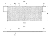
- 2A is a top view of the first electrode sheet
- FIG. 2B is a left side view thereof
- 3A is a top view of the second electrode sheet
- FIG. 2B is a left side view thereof
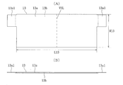
- 4A is a top view of the third electrode sheet
- FIG. 4B is a left side view thereof
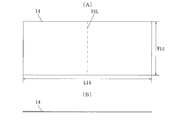
- 5A is a top view of the separate sheet
- FIG. 4B is a left side view thereof.
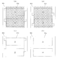
- 6 (A) to 6 (D) are diagrams illustrating a method of creating the first electrode sheet, the second electrode sheet, the third electrode sheet, and the separate sheet.
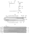
- FIG. 7A is a top view showing a state in which the first electrode sheet, the second electrode sheet, the third electrode sheet, and the separate sheet are stacked, and FIG. 7B is a left side view thereof.
- FIG. 8A is a top view showing a state where the stack shown in FIG. 7A is folded and overlapped, and FIG. 8B is an enlarged left side view thereof.
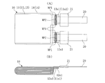
- 9A is a top view showing a state in which the lead connecting portions of the folded product shown in FIG. 8A are mutually coupled, FIG. 9B is an enlarged left side view, and FIG. 9C is FIG. It is an expanded sectional view which follows the S1-S1 line of B).
- FIG. 10A is a top view showing a state in which leads are coupled to the power storage element shown in FIG.
- FIG. 9A, and FIG. 10B is a left side view thereof.
- 11A is a top view of the package sheet
- FIG. 11B is a left side view thereof
- FIG. 11C is an enlarged cross-sectional view of a portion X1 in FIG. 11B.
- FIG. 12 is a top view showing a state where the storage element is inserted into the recess of the package sheet.
- FIG. 13 is a top view showing a state in which the package sheets are folded and overlapped.
- FIG. 14 is a top view showing a state where the left and right portions of the package intermediate product shown in FIG. 13 are heat-sealed.
- FIG. 15 is a top view showing a state where the front portion of the package intermediate product shown in FIG. 14 is heat-sealed.
- FIG. 16A and 16B are enlarged cross-sectional views corresponding to FIG. 9C showing an example in which a misalignment prevention protrusion is provided on the collecting electrode layer of the electrode sheet.
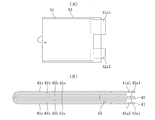
- 17A is a top view of a lithium ion capacitor to which the present invention is applied
- FIG. 17B is a left side view thereof
- FIG. 17C is a front view thereof.
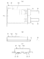
- 18A is a top view of the first electrode sheet
- FIG. 18B is a left side view thereof.
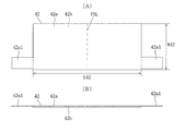
- FIG. 19A is a top view of the second electrode sheet
- FIG. 19B is a left side view thereof.
- FIG. 20A is a top view of the separate sheet
- FIG. 20B is a left side view thereof.
- FIG. 21A to 21C are diagrams showing a method of creating the first electrode sheet, the second electrode sheet, and the separate sheet.
- FIG. 22A is a top view showing a state in which the first electrode sheet, the second electrode sheet, and the separate sheet are stacked, and FIG. 22B is a left side view thereof.
- FIG. 23A is a top view showing a state where the stack shown in FIG. 22A is folded and overlapped, and FIG. 23B is an enlarged left side view thereof.
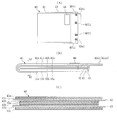
- 24A is a top view showing a state in which the lead connecting portions of the bent product shown in FIG. 23A are mutually coupled, FIG. 24B is an enlarged left side view, and FIG. 24C is FIG. It is an expanded sectional view which follows the S2-S2 line of B).
- FIG. 22A is a top view showing a state in which the first electrode sheet, the second electrode sheet, and the separate sheet are stacked
- FIG. 22B is a left side view thereof.
- FIG. 23A is a top view
- FIG. 25A is a top view showing a state in which leads are coupled to the power storage element shown in FIG. 24A
- FIG. 25B is a left side view thereof.
- 26A is a top view of the package sheet
- FIG. 26B is a left side view thereof
- FIG. 26C is an enlarged cross-sectional view of a portion X2 in FIG.
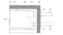
- FIG. 27 is a top view showing a state where the storage element is inserted into the recess of the package sheet.
- FIG. 28 is a top view showing a state in which the package sheets are folded and overlapped.
- FIG. 29 is a top view showing a state where the right side portion and the front side portion of the package intermediate product shown in FIG. 28 are heat-sealed.
- 30 is a top view showing a state in which the left side portion of the package intermediate product shown in FIG. 29 is heat-sealed.
- the electric double layer capacitor includes a power storage element 10, a pair of leads 20 connected to the power storage element 10, and a package 30 enclosing the power storage element 10 so that a part of the pair of leads 20 is exposed. I have.
- FIG. 1A the front, back, right, left, bottom, and top of FIG. 1A are referred to as top, bottom, front, back, left, and right, respectively. These corresponding directions are referred to as up, down, front, back, left and right, respectively.
- the first electrode sheet 11 shown in FIGS. 2A and 2B, the second electrode sheet 12 shown in FIGS. 3A and 3B, and FIG. A third electrode sheet 13 shown in (A) and FIG. 4 (B) and a separate sheet 14 shown in FIGS. 5 (A) and 5 (B) are prepared.
- the first electrode sheet 11 includes a rectangular collector electrode layer 11a having predetermined front and rear dimensions L11 and left and right dimensions W11, and an upper surface of the collector electrode layer 11a. It has a polarizable electrode layer 11b formed by a method such as coating over the entire area (note that the drawing shows that the front end and the rear end of the polarizable electrode layer 11b are slightly inserted into each lead connecting portion 11a1). .
- the collector electrode layer 11a is made of a conductive material such as aluminum or platinum and has a thickness of 5 to 50 ⁇ m.
- the polarizable electrode layer 11b is made of an active material such as PAS (polyacenic organic semiconductor) or activated carbon, and has a thickness of 10 to 50 ⁇ m.
- rectangular lead connection portions 11a1 are integrally provided on the right side of both ends in the front-rear direction of the collector electrode layer 11a with the same thickness as the collector electrode layer 11a.
- the second electrode sheet 12 is a rectangular collector electrode having the same front-rear dimension L12 as the front-rear dimension L11 and the left-right dimension W12 same as the left-right dimension W11.
- a polarizable electrode layer 12b formed by a technique such as coating on the entire upper surface and lower surface of the collector electrode layer 12a (in the drawing, the front end and the rear end of the polarizable electrode layer 12b (A portion slightly inserted into the lead connecting portion 12a1 is shown).
- the material and thickness of the collector electrode layer 12a are the same as those of the collector electrode layer 11a, and the material and thickness of each polarizable electrode layer 12b are the same as those of the polarizable electrode layer 11b.
- a lead connector 12a1 having the same shape as the lead connector 11a1 is integrally provided with the same thickness as the collector electrode layer 12a.
- the third electrode sheet 13 is a rectangular collector electrode having the same front-rear dimension L13 as the front-rear dimension L11 and the left-right dimension W13 as the left-right dimension W11.
- a polarizable electrode layer 13b formed by a technique such as coating on the entire lower surface of the collector electrode layer 13a.
- the front end and the rear end of the polarizable electrode layer 13b are the lead connection portions. 13a1 is shown a little in).
- the material and thickness of the collector electrode layer 13a are the same as those of the collector electrode layer 11a, and the material and thickness of the polarizable electrode layer 13b are the same as those of the polarizable electrode layer 11a.
- a lead connector 13a1 having the same shape as the lead connector 11a1 is located at the same position as the lead connector 11a1 and has the same thickness as the collector electrode layer 13a. Now, it is provided integrally.
- the top-view shape of the collector electrode layer 13a (excluding the lead connection portion 13a1) of the third electrode sheet 13 is the same.
- the top view shape of the polarizable electrode layer 11b of the first electrode sheet 11 and the bottom view shape of the polarizable electrode layer 12b on the bottom surface side of the second electrode sheet 12 are the same.
- the top view shape of the polarizable electrode layer 12 b on the top surface side of the second electrode sheet 12 is the same as the bottom view shape of the polarizable electrode layer 13 b of the third electrode sheet 13.
- the polarizable electrode layer 12b on the upper surface side of the second electrode sheet 12 and the polarizable electrode layer 13b of the third electrode sheet 13 are arranged in the left-right direction or front-back direction of the polarizable electrode layer 11b of the first electrode sheet 11. The shape is inverted 180 degrees in the direction.
- the collector electrode layer 11a (including the lead connection portion 11a1) and the polarizable electrode layer 11b of the first electrode sheet 11 have a line symmetrical shape with respect to the reference line VSL at the center in the front-rear direction shown in FIG. It is made.
- the collector electrode layer 12a (including the lead connection portion 12a1) of the second electrode sheet 12 and each polarizable electrode layer 12b have a line-symmetric shape with respect to the reference line VSL at the center in the front-rear direction shown in FIG. ing.
- the collector electrode layer 13a (including the lead connection portion 13a1) of the third electrode sheet 13 and the polarizable electrode layer 13b have a line-symmetric shape with respect to the reference line VSL at the center in the front-rear direction shown in FIG. ing.
- the separate sheet 14 has a rectangular shape having a front-rear dimension L14 slightly larger than the front-rear dimension L11 and a left-right dimension W14 slightly larger than the left-right dimension W11. Shape.
- the separate sheet 14 is made of an ion permeable sheet such as a cellulose sheet or a plastic sheet, and has a thickness of about 10 to 50 ⁇ m.
- Each of the first electrode sheet 11, the second electrode sheet 12, the third electrode sheet 13, and the separate sheet 14 described above is formed of material sheets BS1 to BS4 as shown in FIGS. 6 (A) to 6 (D). Can be easily obtained by cutting along the virtual lines PL1 to PL4 and extracting the inner part.
- the material sheet BS1 for the first electrode sheet 11 has a band-shaped polarizable electrode layer formed on the upper surface of the band-shaped collector electrode layer
- the material sheet BS2 for the second electrode sheet 12 has the band-shaped collector electrode.
- a band-shaped polarizable electrode layer is formed on the upper and lower surfaces of the electrode layer, and a material sheet BS3 for the third electrode sheet 13 is formed by forming a band-shaped polarizable electrode layer on the lower surface of the band-shaped collector electrode layer. .
- the first electrode sheet 11 prepared in advance, The second electrode sheet 12, the third electrode sheet 13, and the two separate sheets 14 are arranged in the order from the bottom, the first electrode sheet 11, the separate sheet 14, the second electrode sheet 12, the separate sheet 14, and the third electrode sheet. Stack up to 13.
- the outer edges of the collecting electrode layers 11a, 12a, and 13a of the first electrode sheet 11, the second electrode sheet 12, and the third electrode sheet 13 coincide in the stacking direction, and the first electrode sheet 11 and the third electrode
- the outer edges of the lead connecting portions 11a1 and 13a1 of the sheet 13 are made to coincide in the stacking direction.
- the outer edges of the two separate sheets 14 protrude outward from the outer edges of the collector electrode layers 11a, 12a, and 13a, and the outer edges of the separate sheets 14 coincide with each other in the stacking direction. Further, the protruding lengths of the lead connecting portions 11a1, 12a1, and 13a1 of the first electrode sheet 11, the second electrode sheet 12, and the third electrode sheet 13 from the separate sheets 14 are made the same.
- the polarizable electrode layer 11b of the first electrode sheet 11 and the lower polarizable electrode layer 12b of the second electrode sheet 12 are in close contact with the lower separate sheet 14, and the polarizability of the upper side of the second electrode sheet 12 is increased.
- a stacked body (no symbol) in which the electrode layer 12b and the polarizable electrode layer 13b of the third electrode sheet 13 are in close contact with the upper separate sheet 14 is obtained.
- FIGS. 8A and 8B the left portion of the stack shown in FIG. 7A is bent upward along the reference line VSL in the front-rear direction center. , And superimpose the left part on the right part.
- the outer edges of the lead connection portions 11a1 and 13a1 of the first electrode sheet 11 and the third electrode sheet 13 are matched in the superposition direction, and the lead connection portions 12a1 of the second electrode sheet 12 The outer edges should match in the overlapping direction.
- the first electrode sheet 11, the second electrode sheet 12, the third electrode sheet 13, and the two separate sheets 14 are folded in two at an angle of about 180 degrees with the reference line VSL as a boundary. 11, each lead connection portion 11 a 1 and each lead connection portion 13 a 1 of the third electrode sheet 13 face each other, and each lead connection portion 12 a 1 of the second electrode sheet 12 faces each other. It is done.
- each lead connection portion 11a1 and the third electrode of the first electrode sheet 11 facing each other in the folded product shown in FIG. 8A are overlapped, and the two right and left sides are directly joined by a technique such as spot welding, ultrasonic welding or caulking to mutually connect the lead connection parts 11a1 and 13a1. (Refer to the joining point WP1).
- the lead connection portions 12a1 of the second electrode sheet 12 facing each other in the non-contact position with the lead connection portions 11a1 and 13a1 are overlapped, and a method such as spot welding, ultrasonic welding, caulking or the like is performed at two positions on both sides in the left-right direction.
- the lead connecting portions 12a1 are joined together directly (see the joining location WP1).
- the first electrode sheet 11, the second electrode sheet 12, the third electrode sheet 13, and the two separate sheets 14 are folded in two at an angle of about 180 degrees with the reference line VSL as a boundary.
- 11 is connected to each lead connecting portion 11a1 of the third electrode sheet 13, and each lead connecting portion 12a1 of the second electrode sheet 12 is connected to each other. can get.
- FIG. 10 the thickness of the collector electrode layer 11a and the polarizable electrode layer 11b of the first electrode sheet 11 and the collector electrode of the second electrode sheet 12 are shown.
- the thickness of the layer 12a and each polarizable electrode layer 12b, the thickness of the collector electrode layer 13a and polarizable electrode layer 13b of the third electrode sheet 13, and the thickness of the separate sheet 14 are shown thicker than the actual ones. From the relationship, the vertical dimension (overall thickness) of FIGS. 7B, 8B, 9B, and 9C is also thicker than the actual one.
- the vertical dimension (overall thickness) of (B) is 270 ⁇ m, and the vertical dimension (overall thickness) of FIGS. 8B, 9B, and 9C is 540 ⁇ m.
- FIG. 9B for convenience of illustration, in order to explain the coupling of the lead connection portions 11a1 and 13a1 and the coupling of the lead connection portions 12a1 in the bent form, some lead connection portions are shown. Although shown in a stretched manner, as can be understood from the above description, in practice, the lead connection portion can be coupled without such a stretch.
- the lead 20 shown in FIGS. 10A and 10B is prepared.
- the lead 20 is formed in a strip shape from a conductive material such as aluminum, platinum, or copper, and has a thickness of 50 to 100 ⁇ m.
- a metal film for facilitating connection of the lead 20 to an electrode pad or the like may be formed on the end surface of the lead 20 by a technique such as electrolytic plating.
- a seal reinforcing material 21 made of the same material as that of the later-described seal layer LA3 is provided at a position corresponding to the front side portion of the seal region 31c of the later-described package sheet 31 on the surface of the lead 20 so as to surround the position.
- the seal reinforcing material 21 is formed by a method of sandwiching the lead 20 between two sheets, a method of surrounding the lead 20 with one sheet of material, a method of applying a liquid material to the surface of the lead 20, and the like. ing.
- one end of one lead 20 is placed on each of the lead connecting portions 11a1 and 13a1 previously coupled, and the one end is spot welded or super welded.
- the lead 20 is directly joined by a technique such as sonic welding or caulking, and the lead 20 is joined to each of the lead connecting portions 11a1 and 13a1 previously joined (see the joining point WP2).
- one end of the other lead 20 is placed on each lead connecting portion 12a1 that has been joined first, and the one end is directly joined by a technique such as spot welding, ultrasonic welding, caulking, or the like.
- the lead 20 is coupled to each lead connecting portion 12a1 (see the joining point WP2).
- each lead 20 is smaller than the lead connecting portions 11a1, 12a1, and 13a1, and the joint location WP2 is located inside the left and right joint locations WP1, and If these joint locations WP1 and WP2 are aligned, it is possible to accurately perform individual joints by suppressing the failure of joint failure due to overlapping of joint regions, and between the left and right joint locations WP1 and WP2. , That is, the electrical resistance between one lead 20 and the collector electrode layers 11a and 13a, and the electrical resistance between the other lead 20 and the collector electrode layer 12a, respectively.
- the package sheet 31 shown in FIGS. 11A to 11C is prepared.
- the package sheet 31 is composed of a three-layer laminate film in which a protective layer LA1, a barrier layer LA2, and a seal layer LA3 are sequentially laminated.
- the protective layer LA1 is made of a heat-resistant plastic such as nylon or polyethylene phthalate and has a thickness of 10 to 50 ⁇ m.
- the barrier layer LA2 is made of a metal such as aluminum or a metal oxide, and has a thickness of 10 to 50 ⁇ m.
- the seal layer LA3 is made of a thermoplastic plastic such as polypropylene or modified polypropylene and has a thickness of 30 to 50 ⁇ m.
- the package sheet 31 has a rectangular shape having a predetermined front-rear dimension L31 and a left-right dimension W31, and has a rectangular parallelepiped shape on the right side of the center in the front-rear direction. It has the overhang
- the depth of the recess 31 b is slightly larger than the vertical dimension (overall thickness) of the electricity storage element 10, and its top view outline is slightly larger than the top view outline of the electricity storage element 10.
- the seal layer LA3 is located on the upper surface side.
- each seal reinforcing member 21 is placed on the front portion of the seal region 31c. Since the front and rear dimensions of each seal reinforcing member 21 are formed to be slightly larger than the front and rear dimensions of the front portion of the seal region 31c, when the power storage element 10 is inserted into the recess 31b, the front end of each seal reinforcing member 21 is the seal region. It protrudes slightly outward from the front end of the front portion of 31c.
- the package intermediate product shown in FIG. 13 is turned upside down, and heat is applied to the left and right portions thereof to heat-seal the sealing layer LA3 facing each other, and the package is heat-sealed. After the left and right portions are bent upward, heat is applied again to the bent portion 31d to increase the reliability of heat sealing (see heat sealing portion HS).
- an electric double layer capacitor (see FIGS. 1A to 1C) having a structure in which the storage element 10 is enclosed in the package 30 together with the electrolytic solution ES is obtained.
- the sealing layer LA3 of the package sheet 31 is not so large, the lead 20 and the barrier layer LA2 are in contact with each other depending on the molten state when the front portion of the package intermediate product is heat sealed. There is a risk that.
- the electric storage element 10 of the electric double layer capacitor described above has a form (see FIG. 9B) in which the stack shown in FIG. 7A is folded along the reference line VSL (see FIG. 9B).
- the electrode layer 13b and the two separate sheets 14 are continuous through the bent portions. Therefore, even if the layer structure on the cross section is the same as that of the conventional power storage element, the edge regions in the polarizable electrode layers 11b, 12b, and 13b can be reduced as compared with the conventional power storage element.
- the power storage element 10 of the electric double layer capacitor described above is considered that one charge / discharge cell is constituted by the collector electrode layer, the polarizable electrode layer, the separate sheet, the polarizable electrode layer, and the collector electrode layer. From the layer structure shown in FIG. 9C, the power storage element 10 also appears to have four charge / discharge cells. However, the power storage element 10 has the bent form shown in FIG. 9B, and the collector electrode layer 11 a and polarizable electrode layer 11 b of the first electrode sheet 11 and the collector electrode layer 12 a of the second electrode sheet 12.
- the power storage element 10 is 1 This can be represented by an equivalent circuit in which two charge / discharge cells are electrically connected in parallel to the pair of leads 20.
- the number of charge / discharge cells can be halved even if the layer structure on the cross section is the same as that of the conventional power storage device, so the range of charge / discharge characteristics is limited by reducing the number of charge / discharge cells. can do. Therefore, adverse effects caused by variations in charge / discharge characteristics, specifically, charge / discharge is biased in charge / discharge cells having good charge / discharge characteristics, and physicochemical damage is accumulated in the charge / discharge cells. It is possible to reliably suppress the occurrence of problems such as deterioration of the charge / discharge characteristics and the reduction of life.
- the electric storage element 10 of the electric double layer capacitor described above has the bent form shown in FIG. 9B, and each lead connecting portion 11 a 1 of the first electrode sheet 11 and each lead of the third electrode sheet 13.
- the connecting portions 13a1 are mutually coupled, and the lead connecting portions 12a1 of the second electrode sheet 12 are mutually coupled.
- the polarizable electrode layer 11 b of the first electrode sheet 11 located on the outermost side of the electricity storage element 10 is in close contact with the inner separate sheet 14, and the separate sheet 14 is one polarizable electrode layer of the second electrode sheet 12.
- the other polarizable electrode layer 12b of the second electrode sheet 12 is in close contact with the inner separate sheet 14, and the separate sheet 14 is in close contact with the polarizable electrode layer 13b of the third electrode sheet 13.
- the lead connection portions 11a1 of the first electrode sheet 11 and the lead connection portions 13a1 of the third electrode sheet 13 are mutually coupled, and the lead connection portions 12a1 of the second electrode sheet 12 are coupled to each other.
- the first electrode sheet 11, the second electrode sheet 12, the third electrode sheet 13, and each separate sheet 14 that constitute the electricity storage element 10 by mutually coupling It can be determined relative position of the longitudinal direction and lateral direction accurately.
- the first electrode sheet 11, the second electrode sheet 12, the third electrode sheet 13 and the two separate sheets 14 constituting the electricity storage element 10 are less likely to be displaced from each other.
- the process of manufacturing, the process of using the manufactured electric double layer capacitor, and the like it is possible to reliably suppress the shape of the power storage element 10 from being deformed or the deterioration of its charge / discharge characteristics due to the displacement.
- FIG. 16A and FIG. 16B show examples in which at least one of the first electrode sheet 11 and the third electrode sheet 13 and the second electrode sheet 12 are provided with misalignment prevention protrusions, respectively.
- the misalignment prevention protrusion 11a2 having a height higher than the thickness of the polarizable electrode layer 11b is formed on the outer edge of the collector electrode layer 11a of the first electrode sheet 11.
- a misalignment prevention protrusion 12a2 having a height higher than the thickness of the polarizable electrode layer 12b is provided on the outer edge of the collector electrode layer 12a of the second electrode sheet 12, and
- a misalignment prevention protrusion 13a2 having a height higher than the thickness of the polarizable electrode layer 13b is provided.
- misalignment prevention protrusions 11a2, 12a2, and 13a2 may have a shape that is continuous along the outer edge or a shape that is not continuous along the outer edge. However, in order to prevent a two-dimensional misalignment, the protrusions 11a2, 12a2, and 13a2 are provided at at least two locations on the outer edge. It is desirable.
- the misalignment prevention protrusion 11a2 of the first electrode sheet 11 bites into the adjacent separate sheet 14 in a non-penetrating state
- the misalignment prevention protrusion 12a2 of the second electrode sheet 12 is adjacent to the separate sheet 14.
- the position shift prevention protrusion 13a2 of the third electrode sheet 13 bites into the adjacent separate sheet 14 in a non-penetrating state.
- the misalignment prevention protrusions 12a2 and 13a2 bite into the separate sheets 14 appearing in the second layer and the third layer from the top so as to face in the vertical direction, but the misalignment prevention protrusions are adjusted by adjusting the biting depth. 12a2 and 13a2 are prevented from contacting each other.
- the misalignment prevention protrusion 11a2 having a height higher than the thickness of the polarizable electrode layer 11b is formed on the outer edge of the collector electrode layer 11a of the first electrode sheet 11.
- a misalignment prevention protrusion 12a2 having a height larger than the thickness of the polarizable electrode layer 12b is provided on the outer edge of the collector electrode layer 12a of the second electrode sheet 12, and the collector electrode layer 13a of the third electrode sheet 13 is provided. Is not provided with a misalignment prevention protrusion.
- These misalignment prevention protrusions 11a2 and 12a2 may have a shape that is continuous along the outer edge or a shape that is not continuous along the outer edge. However, in order to prevent two-dimensional misalignment, the protrusions 11a2 and 12a2 must be provided at at least two locations on the outer edge. Is desirable.
- the misalignment prevention protrusion 11a2 of the first electrode sheet 11 bites into the adjacent separate sheet 14 in a non-penetrating state
- the misalignment prevention protrusion 12a2 of the second electrode sheet 12 is adjacent to the separate sheet 14.
- the position shift prevention protrusion 13a2 of the third electrode sheet 13 bites into the adjacent separate sheet 14 in a non-penetrating state.
- the reason why the misalignment prevention protrusion is not provided on the collector electrode layer 13a of the third electrode sheet 13 is that the collector electrode layer 11a of the first electrode sheet 11 and the collector electrode layer 13a of the third electrode sheet 13 are as described above.
- the relative positions in the front-rear direction and the left-right direction are determined by coupling the lead connecting portions 11a1 and 13a1 to each other.
- FIG. 6C In order to form the misalignment prevention protrusions 11a2, 12a2, and 13a2, in addition to a technique of deforming the outer edge by pressing an appropriate processing jig against the outer edges of the collector electrode layers 11a, 12a, and 13a, FIG. In the production method described with reference to FIG. 6C, a method of using a press cutting blade for cutting along the phantom lines PL1 to PL3 and causing sagging due to the press cutting at the outer edges of the collector electrode layers 11a, 12a, and 13a can be adopted.
- the first electrode sheet 11, the second electrode sheet 12, and the third electrode sheet constituting the power storage elements 10-1 and 10-2 are used.
- the misalignment between the 13 sheets and the two separate sheets 14 can be prevented more reliably, so that the misalignment occurs in the process of manufacturing the electric double layer capacitor, the process of using the electric double layer capacitor after manufacture, and the like.
- the direction of the misregistration prevention protrusion is not limited to FIGS. 16A and 16B.
- one misalignment prevention protrusion 12a2 in the left-right direction of the collector electrode layer 12a of the second electrode sheet 12 is provided.
- the left and right direction other side may be upward and the other side of the third electrode sheet 13 of the third electrode sheet 13 in the left and right direction misalignment prevention protrusion 13a2 may be downward and the left and right direction other side may be upward and the lower position misalignment prevention protrusion. You may make it make 13a2 bite into the opposing collector layer 13a.
- FIG. 17 to 30 show an embodiment in which the present invention is applied to a lithium ion capacitor.
- the lithium ion capacitor includes a power storage element 40, a pair of leads 20 connected to the power storage element 40, and a package 50 enclosing the power storage element 10 so that a part of the pair of leads 20 is exposed. ing.
- FIG. 17A the front, back, right, left, bottom, and top of FIG. 17A are referred to as top, bottom, front, back, left, and right, respectively. These corresponding directions are referred to as up, down, front, back, left and right, respectively.
- sticker reinforcement 21 is the same as what was described in 1st Embodiment, it demonstrates using the same code
- the first electrode sheet 41 shown in FIGS. 18A and 18B, the second electrode sheet 42 shown in FIGS. 19A and 19B, and FIG. (A) and a separate sheet 43 shown in FIG. 20 (B) are prepared.
- the first electrode sheet 41 includes a rectangular collector electrode layer 41a having a predetermined front-rear dimension L41 and a left-right dimension W41, and an upper surface of the collector electrode layer 41a.
- a polarizable electrode layer 41b formed by a technique such as coating is provided in a region excluding both end portions in the front-rear direction.
- the front-rear dimension L41b of the polarizable electrode layer 41b is slightly smaller than the front-rear dimension L41.
- the collector electrode layer 41a is made of a conductive material such as copper and has a thickness of 5 to 50 ⁇ m.
- the polarizable electrode layer 41b is made of a material capable of reversibly supporting lithium ions such as graphite and has a thickness of 50 to 100 ⁇ m.
- a rectangular lead connection portion 41a1 is integrally provided with the same thickness as the collector electrode layer 41a on the right side of both ends in the front-rear direction of the collector electrode layer 41a.
- the second electrode sheet 42 has a front-rear dimension L42 slightly smaller than the front-rear dimension L41b and a left-right dimension W42 slightly smaller than the left-right dimension W41.
- a polarizable electrode layer 42b formed on the entire lower surface of the collector electrode layer 42a by a technique such as coating.
- the difference between the front-rear dimension L42 of the collector electrode layer 42a and the front-rear dimension L41b and the difference between the left-right dimension W42 and the left-right dimension W41 are about 0.3 to 2.0 mm in actual dimensions.
- the collector electrode layer 42a is made of a conductive material such as aluminum and has a thickness of 5 to 100 ⁇ m.
- the polarizable electrode layer 42b is made of a material capable of reversibly supporting lithium ions such as activated carbon, and has a thickness of 5 to 200 ⁇ m. Further, on the left side of both ends of the collector electrode layer 42a in the front-rear direction, a rectangular lead connection portion 42a1 having a narrower left-right dimension (width) than the lead connection portion 41a1 and a larger front-rear dimension is provided on the collector electrode layer 42a. Are integrally provided with the same thickness.
- the distance between the front end of the front lead connection portion 42a1 and the rear end of the rear lead connection portion 42a1 is such that the front end of the front lead connection portion 41a1 and the rear end of the rear lead connection portion 41a1 in the first electrode sheet 41 are as follows. Is the same as the distance.
- the top view shape of the collector electrode layer 41a (excluding the lead connection portion 41a1) of the first electrode sheet 41 is more than the top view shape of the collector electrode layer 42a (excluding the lead connection portion 42a1) of the second electrode sheet 42. large.
- the top view shape of the polarizable electrode layer 41 b of the first electrode sheet 41 is larger than the bottom view shape of the polarizable electrode layer 42 b of the second electrode sheet 42.
- the collector electrode layer 41a (including the lead connection portion 41a1) and the polarizable electrode layer 41b of the first electrode sheet 41 have a line-symmetric shape with respect to the reference line VSL at the center in the front-rear direction shown in FIG. It is made.
- the collector electrode layer 42a (including the lead connection portion 42a1) and the polarizable electrode layer 42b of the second electrode sheet 42 form a line symmetry with respect to the reference line VSL at the center in the front-rear direction shown in FIG. Yes.
- the separate sheet 43 is a rectangle having a front-rear dimension L43 slightly larger than the front-rear dimension L41 and a left-right dimension W43 slightly larger than the left-right dimension W41. Shape.
- the separate sheet 43 is made of an ion permeable sheet such as a cellulose sheet or a plastic sheet, and has a thickness of about 10 to 50 ⁇ m.
- Each of the first electrode sheet 41, the second electrode sheet 42, and the separate sheet 43 described above is formed by replacing the material sheets BS11 to BS13 with virtual lines PL11 to PL13, as shown in FIGS. 21 (A) to 21 (C). Can be obtained by a method of cutting along and cutting out the inner part.
- the material sheet BS11 for the first electrode sheet 41 has a band-shaped polarizable electrode layer formed on the upper surface of the band-shaped collector electrode layer
- the material sheet BS12 for the second electrode sheet 42 has a band-shaped collector electrode.
- a band-shaped polarizable electrode layer is formed on the upper surface of the electrode layer.
- the first electrode sheet 41 previously prepared,
- the second electrode sheet 42 and the separate sheet 43 are stacked so that the order from the bottom becomes the first electrode sheet 41, the separate sheet 43, and the second electrode sheet 42.
- the outer edge of the polarizable electrode layer 41b of the first electrode sheet 41 protrudes outside the outer edge of the polarizable electrode layer 42b of the second electrode sheet 42, and the outer edge of the separate sheet 43 is the first edge.
- the electrode sheet 41 protrudes outward from the outer edge of the collector electrode layer 41a. Further, the protruding lengths of the lead connecting portions 41a1 and 42a1 of the first electrode sheet 41 and the second electrode sheet 42 from the separate sheet 43 are made the same.
- the left side portion of the stacked body shown in FIG. 22A is bent upward along the reference line VSL in the front-rear direction center. , And superimpose the left part on the right part.
- the outer edges of the lead connection portions 41a1 of the first electrode sheet 41 are matched in the superposition direction, and the outer edges of the lead connection portions 42a1 of the second electrode sheet 42 are matched in the superposition direction.
- the first electrode sheet 41, the second electrode sheet 42, and the separate sheet 43 are folded in half at an angle of about 180 degrees with the reference line VSL as a boundary, and the lead connection portions 11a1 of the first electrode sheet 11 face each other.
- a folded product (no symbol) having a form in which the lead connection portions 12a1 of the second electrode sheet 12 face each other is obtained.
- each lead connection portion 41a1 and each lead connection portion 42a1 of the second electrode sheet 42 facing each other in a non-contact position are overlapped, and spot welding or ultrasonic waves are performed at two locations on both sides in the left-right direction with the separate sheet 43 interposed therebetween.
- the respective lead connecting portions 42a1 are joined together by a technique such as welding or caulking (see the joining location WP11).
- a lithium sheet for lithium doping 44 is attached to the upper surface of the collector electrode layer 41a of the first electrode sheet 41 by a technique such as pressure bonding.
- the first electrode sheet 41, the second electrode sheet 42, and the separate sheet 43 are folded in half at an angle of about 180 degrees with the reference line VSL as a boundary, and the lead connection portions 41a1 of the first electrode sheet 41 are mutually connected.
- the electric storage element 40 having a configuration in which the lead connecting portions 12a1 of the second electrode sheet 12 are coupled to each other is obtained.
- FIG. 25 the thickness of the collector electrode layer 41a and the polarizable electrode layer 41b of the first electrode sheet 41 and the collector electrode of the second electrode sheet 42 are shown. From the relationship in which the thickness of the layer 42a and each polarizable electrode layer 42b and the thickness of the separate sheet 43 are shown to be thicker than the actual thickness, FIG. 22 (B), FIG. 23 (B), FIG. And the vertical dimension (overall thickness) of FIG.24 (C) is also thicker than an actual thing.
- the thickness of the collector electrode layer 41a and the polarizable electrode layer 41b of the first electrode sheet 41, the thickness of the collector electrode layer 42a and the polarizable electrode layer 42b of the second electrode sheet 42, and the thickness of the separate sheet 43 are 5
- the vertical dimension (overall thickness) of FIG. 22B is 300 ⁇ m in actuality
- FIG. The vertical dimension (overall thickness) of 24 (B) and FIG. 24 (C) is 600 ⁇ m.
- FIG. 24B for convenience of illustration, in order to explain the coupling of the lead connection portions 41a1 and the coupling of the lead connection portions 42a1 in the bent form, a part of the lead connection portions is extended. Although shown, as can be understood from the above description, in actuality, the lead connection portion can be coupled without such extension.
- the lead 20 shown in FIG. 25 (A) and FIG. 25 (B) is prepared.
- the lead 20 is formed in a strip shape from a conductive material such as aluminum, platinum, or copper, and has a thickness of 50 to 100 ⁇ m.
- a metal film for facilitating connection of the lead 20 to an electrode pad or the like may be formed on the end surface of the lead 20 by a technique such as electrolytic plating.
- a seal reinforcing material 21 made of the same material as that of the later-described seal layer LA3 is provided at a position corresponding to the front side portion of the seal region 51c of the later-described package sheet 51 on the surface of the lead 20 so as to surround the position.
- the seal reinforcing material 21 is formed by a method of sandwiching the lead 20 between two sheets, a method of surrounding the lead 20 with one sheet of material, a method of applying a liquid material to the surface of the lead 20, and the like. ing.
- one end of one lead 20 is placed on a portion protruding from the separate sheet 43 of each lead connecting portion 41a1 previously coupled, One end is directly joined by a technique such as spot welding, ultrasonic welding, caulking, etc., and the lead 20 is joined to each lead connecting portion 41a1 that has been joined first (see the joint location WP12).
- one end of the other lead 20 is placed on the portion of the lead connecting portion 42a1 that has been previously coupled and protrudes from the separate sheet 43, and the one end is directly attached by a technique such as spot welding, ultrasonic welding, or caulking.
- the leads 20 are joined to the lead connecting portions 42a1 that have been joined together (see the joining location WP12).
- the package sheet 51 is composed of a three-layer laminate film in which a protective layer LA1, a barrier layer LA2, and a seal layer LA3 are sequentially laminated.
- the protective layer LA1 is made of a heat-resistant plastic such as nylon or polyethylene phthalate and has a thickness of 10 to 50 ⁇ m.
- the barrier layer LA2 is made of a metal such as aluminum or a metal oxide, and has a thickness of 10 to 50 ⁇ m.
- the seal layer LA3 is made of a thermoplastic plastic such as polypropylene or modified polypropylene and has a thickness of 30 to 50 ⁇ m.
- the package sheet 51 has a rectangular shape having a predetermined front-rear dimension L51 and a left-right dimension W51, and has a rectangular parallelepiped shape on the right side of the center in the front-rear direction. It has the overhang
- the depth of the recess 51 b is slightly larger than the vertical dimension (overall thickness) of the electricity storage element 40, and its top view outline is slightly larger than the top view outline of the electricity storage element 40.
- the portion of the package sheet 51 on the right side of the center in the front-rear direction where the recess 51b does not exist is a seal region 51c, and the seal layer LA3 is located on the upper surface side of the package sheet 51.
- each seal reinforcing member 21 is placed on the front portion of the seal region 51c. Since the front and rear dimensions of each seal reinforcing member 21 are formed to be slightly larger than the front and rear dimensions of the front portion of the seal region 51c, when the power storage element 40 is inserted into the recess 51b, the front end of each seal reinforcing member 21 is the seal region. It protrudes slightly outward from the front end of the front portion of 51c.
- the left side portion of the package sheet 51 shown in FIG. 27 from the center in the front-rear direction is bent upward along the reference line VSL in the figure, and the left side portion is overlaid on the right side portion.
- the package intermediate product shown in FIG. 28 is turned upside down, and then heat is applied to the right side portion thereof to heat-seal the sealing layer LA3 facing each other, and heat is applied to the front side portion. Then, the seal layers LA3 facing each other are heat-sealed with the seal reinforcing members 21 interposed therebetween (see the heat-seal location HS).
- hexafluorination into an electrolytic solution ES for example, propylene carbonate (solvent) is performed using a suitable injection device through the left side portion of the package intermediate product shown in FIG. 29 which is not heat-sealed.
- Lithium phosphate (solute added) is injected into the recess 51b.
- heat is applied to the left side portion of the seal region 51c to heat-seal the seal layers LA3 facing each other (see the heat seal location HS).
- FIGS. 17A to 17C a lithium ion capacitor (see FIGS. 17A to 17C) having a structure in which the storage element 40 is enclosed in the package 50 together with the electrolytic solution ES is obtained.
- the sealing layer LA3 of the package sheet 51 is not so large, the lead 20 and the barrier layer LA2 are in contact with each other depending on the molten state when the front portion of the package intermediate product is heat sealed. There is a risk.
- the above-described storage element 40 of the lithium ion capacitor has a configuration (see FIG. 24B) in which the stack shown in FIG. 22A is folded along the reference line VSL (see FIG. 24B).
- the collector electrode layer 41a and polarizable electrode layer 41b of the first electrode sheet 41, the collector electrode layer 42a and polarizable electrode layer 42b of the second electrode sheet 42, and the separate sheet 43 are continuous through the bent portions. Therefore, even if the layer structure on the cross section is the same as that of the conventional power storage element, the edge regions in the polarizable electrode layers 41b and 42b can be reduced as compared with the conventional power storage element.
- the storage element 40 of the above-described lithium ion capacitor when the storage element 40 of the above-described lithium ion capacitor is considered that one charge / discharge cell is constituted by the collector electrode layer, the polarizable electrode layer, the separate sheet, the polarizable electrode layer, and the collector electrode layer, FIG. According to the layer structure shown in FIG. 24C, the power storage element 40 seems to have two charge / discharge cells. However, the storage element 40 has the bent form shown in FIG. 24B, and the collector electrode layer 41a and polarizable electrode layer 41b of the first electrode sheet 41 and the collector electrode layer 42a of the second electrode sheet 42. Since each polarizable electrode layer 42b and the separate sheet 43 are continuous through the bent portions, the storage element 40 is an equivalent circuit in which one charge / discharge cell is electrically connected to a pair of leads 20. Can be expressed as
- the number of charge / discharge cells can be halved even if the layer structure on the cross section is the same as that of the conventional power storage device, so the range of charge / discharge characteristics is limited by reducing the number of charge / discharge cells. can do. Therefore, adverse effects caused by variations in charge / discharge characteristics, specifically, charge / discharge is biased in charge / discharge cells having good charge / discharge characteristics, and physicochemical damage is accumulated in the charge / discharge cells. It is possible to reliably suppress the occurrence of problems such as deterioration of the charge / discharge characteristics and the reduction of life.
- the above-described storage element 40 of the lithium ion capacitor has the bent form shown in FIG. 24B, and the lead connection portions 41a1 of the first electrode sheet 41 are mutually coupled through the separate sheet 43.
- the lead connection portions 42 a 1 of the second electrode sheet 42 are mutually coupled through a separate sheet 43.
- the polarizable electrode layer 41b of the first electrode sheet 41 located on the outermost side of the power storage element 40 is in close contact with the inner separate sheet 43, and the separate sheet 43 is attached to the polarizable electrode layer 42b of the second electrode sheet 42.
- the lead connection portions 41a1 of the first electrode sheet 41 are mutually coupled via the separate sheet 43, and the lead connection portions 42a1 of the second electrode sheet 42 are connected to the separate sheet 43.
- the relative positions in the front-rear direction and the left-right direction of the first electrode sheet 41, the second electrode sheet 42, and the separate sheet 43 that constitute the power storage element 40 can be accurately determined.
- the process of manufacturing a lithium ion capacitor In the process of using a capacitor or the like, it is possible to reliably suppress the shape of the power storage element 40 from being deformed or the charge / discharge characteristics from being deteriorated due to the positional deviation.
- the misalignment prevention protrusions similar to the misalignment prevention protrusions 11a2, 12a2, and 13a2 shown in FIGS. 16 (A) and 16 (B) are formed on the collector electrode layer 31a of the first electrode sheet 31. If provided on both the outer edge and the outer edge of the collector electrode layer 42 a of the second electrode sheet 42, or only on the outer edge of the collector electrode layer 31 a of the first electrode sheet 31, the first electrode sheet 41, the second electrode sheet 42 and the separate electrode are provided. Since the mutual displacement of the sheets 43 can be prevented more reliably, in the process of manufacturing a lithium ion capacitor, the process of using the lithium ion capacitor after manufacture, etc., the shape of the storage element is caused by the displacement. It can prevent more reliably that it collapses or the charge / discharge characteristic deteriorates.
- the laminated body obtained by overlapping the first electrode sheet 11, the separate sheet 14, the second electrode sheet 12, the separate sheet 14, and the third electrode sheet 13 in this order is folded and overlapped.
- the power storage element 10 is configured, and the stacked body obtained by stacking the first electrode sheet 41, the separate sheet 43, and the second electrode sheet 42 in this order is folded and overlapped.
- the number of sheets of the laminated body before folding may be larger than that of the laminated body shown in the first embodiment (see FIG. 7B).
- the position of the lead connection part 12a1 of the first electrode sheet 11, the separate sheet 14, the second electrode sheet 12, the separate sheet 14, and the second electrode sheet 12 is changed to the position of the lead connection part 11a1 of the first electrode sheet 11. If the electrode sheet, the separate sheet 14, and the electrode sheet in which the position of the lead connection part 13a1 of the third electrode sheet 13 is changed to the position of the lead connection part 12a1 of the second electrode sheet 12 are overlapped in order,
- the charge / discharge cell can constitute three power storage elements, and the same operation and effect as described above can be obtained.
- the present invention is applied to an electric double layer capacitor as a first embodiment, and the present invention is applied to a lithium ion capacitor as a second embodiment.
- the present invention can also be applied to other electrochemical devices such as a redox capacitor and a lithium ion battery, and the same operations and effects as described above can be obtained by the application.
Landscapes
- Engineering & Computer Science (AREA)
- Power Engineering (AREA)
- Microelectronics & Electronic Packaging (AREA)
- Manufacturing & Machinery (AREA)
- Chemical & Material Sciences (AREA)
- Chemical Kinetics & Catalysis (AREA)
- Electrochemistry (AREA)
- General Chemical & Material Sciences (AREA)
- Electric Double-Layer Capacitors Or The Like (AREA)
Abstract
Description
図1~図15は本発明を電気二重層キャパシタに適用した実施形態を示す。この電気二重層キャパシタは、蓄電素子10と、該蓄電素子10に接続された一対のリード20と、該一対のリード20の一部が露出するように蓄電素子10を封入したパッケージ30と、を備えている。
する等の不具合を生じる恐れがある。しかしながら、前記蓄電素子10にあっては各分極性電極層11b、12b及び13bにおけるエッジ領域を従前の蓄電素子に比べて減らすことができるため、前記ダメージが生じることを効果的に抑制し、該ダメージを原因として蓄電素子10全体としての耐電圧特性が低下したり寿命が低下したりする等の不具合を生じることを確実に抑制することができる。
けられ、第2電極シート12の集電極層12aの外縁に分極性電極層12bの厚さよりも高さが大きな位置ずれ防止突起12a2が設けられ、第3電極シート13の集電極層13aの外縁に分極性電極層13bの厚さよりも高さが大きな位置ずれ防止突起13a2が設けられている。これら位置ずれ防止突起11a2、12a2及び13a2は外縁に沿って連続した形状でも外縁に沿って連続しない形状でも良いが、2次元的な位置ずれを防止するには外縁の少なくとも2箇所に設けられていることが望ましい。
図17~図30は本発明をリチウムイオンキャパシタに適用した実施形態を示す。このリチウムイオンキャパシタは、蓄電素子40と、該蓄電素子40に接続された一対のリード20と、該一対のリード20の一部が露出するように蓄電素子10を封入したパッケージ50と、を備えている。
(1)第1実施形態では、第1電極シート11、セパレートシート14、第2電極シート12、セパレートシート14、第3電極シート13の順に重ね合わせて得た積層体を折り曲げて重ね合わせることで蓄電素子10を構成したものを示し、第2実施形態では、第1電極シート41、セパレートシート43、第2電極シート42の順に重ね合わせて得た積層体を折り曲げて重ね合わせることで蓄電素子10を構成したものを示したが、折り曲げる前の積層体のシート数は第1実施形態に示した積層体(図7(B)を参照)よりも増加しても良い。
Claims (6)
- 蓄電素子をパッケージ内に封入した構造を備える電気化学デバイスであって、
該蓄電素子は、集電極層と該集電極層の少なくとも一面に形成された分極性電極層を有する2以上の電極シートが分極性電極層間にセパレートシートを介在して積み重ねられた物を基準線に沿って折り曲げて重ね合わせた形態を有しており、該形態にあって各電極シートの集電極層及び分極性電極層とセパレートシートはそれぞれ折り曲げ箇所を通じて連続している。 - 請求項1に記載の電気化学デバイスにおいて、
前記2以上の電極シートのうち、一方極性として用いられる電極シートの集電極層の両端には前記形態において互いに向き合うリード接続部が設けられていて、且つ、該リード接続部は相互に結合されており、他方極性として用いられる電極シートの集電極層の両端には前記形態において前記電極シートのリード接続部と非接触位置で互いに向き合うリード接続部が設けられていて、且つ、該リード接続部は相互に結合されている。 - 請求項2に記載の電気化学デバイスにおいて、
前記一方極性として用いられる電極シートのリード接続部はセパレートシートを介して相互に結合され、前記他方極性として用いられる電極シートのリード接続部はセパレートシートを介して相互に結合されている。 - 請求項1~3の何れか1項に記載の電気化学デバイスにおいて、
前記積み重ねられた物は、集電極層と該集電極層の一面に形成された分極性電極層を有する第1電極シートと、集電極層と該集電極層の両面に形成された分極性電極層を有する第2電極シートと、集電極層と該集電極層の他面に形成された分極性電極層を有する第3電極シートと、2枚のセパレートシートとを備えていて、2枚のセパレートシートの一方のセパレートシートは第1電極シートの分極性電極層と第2電極シートの一方の分極性電極層との間に介在し、他方のセパレートシートは第2電極シートの他方の分極性電極層と第3電極シートの分極性電極層との間に介在する。
いる。 - 請求項1~3の何れか1項に記載の電気化学デバイスにおいて、
前記積み重ねられた物は、集電極層と該集電極層の一面に形成された分極性電極層を有する第1電極シートと、集電極層と該集電極層の他面に形成された分極性電極層を有する第2電極シートと、セパレートシートとを備えていて、セパレートシートは第1電極シートの分極性電極層と第2電極シートの分極性電極層との間に介在する。 - 請求項1~3の何れか1項に記載の電気化学デバイスにおいて、
前記2以上の電極シートのうち、一方極性として用いられる少なくとも1つの電極シートの集電極層は位置ずれ防止突起を外縁に有していて、且つ、該位置ずれ防止突起は隣接するセパレートシートに非貫通状態で食い込んでおり、他方極性として用いられる少なくとも1つの電極シートの集電極層は位置ずれ防止突起を外縁に有していて、且つ、該位置ずれ防止突起は隣接するセパレートシートに非貫通状態で食い込んでいる。
Priority Applications (3)
| Application Number | Priority Date | Filing Date | Title |
|---|---|---|---|
| CN201080029005.7A CN102473529B (zh) | 2009-07-17 | 2010-06-03 | 电化学装置 |
| US13/383,411 US8804310B2 (en) | 2009-07-17 | 2010-06-03 | Electrochemical device |
| KR1020117027079A KR101227916B1 (ko) | 2009-07-17 | 2010-06-03 | 전기 화학 디바이스 |
Applications Claiming Priority (4)
| Application Number | Priority Date | Filing Date | Title |
|---|---|---|---|
| JP2009-169290 | 2009-07-17 | ||
| JP2009169290 | 2009-07-17 | ||
| JP2010075347A JP5026544B2 (ja) | 2009-07-17 | 2010-03-29 | 電気化学デバイス |
| JP2010-075347 | 2010-03-29 |
Publications (1)
| Publication Number | Publication Date |
|---|---|
| WO2011007624A1 true WO2011007624A1 (ja) | 2011-01-20 |
Family
ID=43449233
Family Applications (1)
| Application Number | Title | Priority Date | Filing Date |
|---|---|---|---|
| PCT/JP2010/059410 Ceased WO2011007624A1 (ja) | 2009-07-17 | 2010-06-03 | 電気化学デバイス |
Country Status (6)
| Country | Link |
|---|---|
| US (1) | US8804310B2 (ja) |
| JP (1) | JP5026544B2 (ja) |
| KR (1) | KR101227916B1 (ja) |
| CN (1) | CN102473529B (ja) |
| TW (1) | TWI437595B (ja) |
| WO (1) | WO2011007624A1 (ja) |
Cited By (1)
| Publication number | Priority date | Publication date | Assignee | Title |
|---|---|---|---|---|
| WO2014192285A1 (ja) * | 2013-05-31 | 2014-12-04 | パナソニックIpマネジメント株式会社 | 薄型電池 |
Families Citing this family (10)
| Publication number | Priority date | Publication date | Assignee | Title |
|---|---|---|---|---|
| US10002717B2 (en) * | 2014-10-30 | 2018-06-19 | General Capacitor, Llc | High performance lithium-ion capacitor laminate cells |
| KR102360413B1 (ko) * | 2015-02-16 | 2022-02-09 | 삼성에스디아이 주식회사 | 이차 전지 |
| HUE046774T2 (hu) | 2015-08-07 | 2020-03-30 | Bosch Gmbh Robert | Telepcella |
| US10833324B2 (en) | 2015-08-25 | 2020-11-10 | Licap Technologies, Inc. | Electrodes with controlled amount of lithium attached and method of making same |
| JP6703826B2 (ja) * | 2015-12-02 | 2020-06-03 | 日東電工株式会社 | フィルム貼り合わせ方法 |
| JP6705689B2 (ja) * | 2016-04-21 | 2020-06-03 | セイコーインスツル株式会社 | 電気化学セル |
| MY195773A (en) | 2016-05-20 | 2023-02-11 | Kyocera Avx Components Corp | Multi-Cell Ultracapacitor |
| JP6705702B2 (ja) * | 2016-06-13 | 2020-06-03 | セイコーインスツル株式会社 | 電気化学セル |
| US11830672B2 (en) | 2016-11-23 | 2023-11-28 | KYOCERA AVX Components Corporation | Ultracapacitor for use in a solder reflow process |
| KR102839856B1 (ko) * | 2021-09-30 | 2025-07-29 | 주식회사 엘지에너지솔루션 | 분리막 적층체 및 이를 포함하는 전극 조립체, 그리고 전극 조립체 제조 방법 |
Citations (5)
| Publication number | Priority date | Publication date | Assignee | Title |
|---|---|---|---|---|
| JPH0864479A (ja) * | 1994-08-24 | 1996-03-08 | Fuji Elelctrochem Co Ltd | 電気化学素子およびその製造方法 |
| JP2000353643A (ja) * | 1999-06-10 | 2000-12-19 | Honda Motor Co Ltd | 電気二重層コンデンサ |
| JP2002043180A (ja) * | 2000-07-31 | 2002-02-08 | Kyocera Corp | 電気二重層コンデンサ |
| JP2003508906A (ja) * | 1999-08-30 | 2003-03-04 | エナジィ・ストーリッジ・システムズ・プロプライエタリー・リミテッド | 電荷蓄積装置 |
| JP2007299855A (ja) * | 2006-04-28 | 2007-11-15 | Nec Tokin Corp | 積層型電気化学デバイス |
Family Cites Families (14)
| Publication number | Priority date | Publication date | Assignee | Title |
|---|---|---|---|---|
| US4761352A (en) * | 1985-05-17 | 1988-08-02 | Eastman Kodak Company | Accordian folded electrode assembly |
| JPH03234016A (ja) | 1990-02-09 | 1991-10-18 | Isuzu Motors Ltd | 電気二重層コンデンサ |
| US5460904A (en) * | 1993-08-23 | 1995-10-24 | Bell Communications Research, Inc. | Electrolyte activatable lithium-ion rechargeable battery cell |
| US6181545B1 (en) * | 1998-09-24 | 2001-01-30 | Telcordia Technologies, Inc. | Supercapacitor structure |
| WO2000034964A1 (en) | 1998-12-05 | 2000-06-15 | Energy Storage Systems Pty. Ltd. | A charge storage device |
| JP2001338848A (ja) | 2000-05-26 | 2001-12-07 | Matsuo Electric Co Ltd | 電気二重層コンデンサ |
| JP4637325B2 (ja) | 2000-06-29 | 2011-02-23 | 京セラ株式会社 | 電気二重層コンデンサ |
| IL155790A0 (en) | 2000-11-09 | 2003-12-23 | Foc Frankenburg Oil Company Es | A supercapacitor and a method of manufacturing such a supercapacitor |
| US20030186117A1 (en) * | 2002-03-27 | 2003-10-02 | Ntk Powerdex, Inc. | Primary lithium battery and method of forming the same |
| US7251122B2 (en) * | 2003-12-22 | 2007-07-31 | Tdk Corporation | Electric chemical capacitor, and method and apparatus for manufacturing electrode for electric chemical capacitor |
| US7629077B2 (en) * | 2004-02-26 | 2009-12-08 | Qinetiq Limited | Pouch cell construction |
| JP4670275B2 (ja) | 2004-08-12 | 2011-04-13 | 日産自動車株式会社 | バイポーラ電池および組電池 |
| US8105714B2 (en) * | 2004-10-29 | 2012-01-31 | Medtronic, Inc. | Lithium-ion battery |
| JP5103822B2 (ja) | 2006-08-14 | 2012-12-19 | ソニー株式会社 | 非水電解質二次電池 |
-
2010
- 2010-03-29 JP JP2010075347A patent/JP5026544B2/ja not_active Expired - Fee Related
- 2010-06-03 CN CN201080029005.7A patent/CN102473529B/zh not_active Expired - Fee Related
- 2010-06-03 KR KR1020117027079A patent/KR101227916B1/ko not_active Expired - Fee Related
- 2010-06-03 US US13/383,411 patent/US8804310B2/en not_active Expired - Fee Related
- 2010-06-03 WO PCT/JP2010/059410 patent/WO2011007624A1/ja not_active Ceased
- 2010-07-16 TW TW099123573A patent/TWI437595B/zh not_active IP Right Cessation
Patent Citations (5)
| Publication number | Priority date | Publication date | Assignee | Title |
|---|---|---|---|---|
| JPH0864479A (ja) * | 1994-08-24 | 1996-03-08 | Fuji Elelctrochem Co Ltd | 電気化学素子およびその製造方法 |
| JP2000353643A (ja) * | 1999-06-10 | 2000-12-19 | Honda Motor Co Ltd | 電気二重層コンデンサ |
| JP2003508906A (ja) * | 1999-08-30 | 2003-03-04 | エナジィ・ストーリッジ・システムズ・プロプライエタリー・リミテッド | 電荷蓄積装置 |
| JP2002043180A (ja) * | 2000-07-31 | 2002-02-08 | Kyocera Corp | 電気二重層コンデンサ |
| JP2007299855A (ja) * | 2006-04-28 | 2007-11-15 | Nec Tokin Corp | 積層型電気化学デバイス |
Cited By (2)
| Publication number | Priority date | Publication date | Assignee | Title |
|---|---|---|---|---|
| WO2014192285A1 (ja) * | 2013-05-31 | 2014-12-04 | パナソニックIpマネジメント株式会社 | 薄型電池 |
| JP6032628B2 (ja) * | 2013-05-31 | 2016-11-30 | パナソニックIpマネジメント株式会社 | 薄型電池 |
Also Published As
| Publication number | Publication date |
|---|---|
| KR20120024605A (ko) | 2012-03-14 |
| US8804310B2 (en) | 2014-08-12 |
| JP2011040711A (ja) | 2011-02-24 |
| KR101227916B1 (ko) | 2013-01-30 |
| CN102473529A (zh) | 2012-05-23 |
| CN102473529B (zh) | 2014-03-12 |
| TWI437595B (zh) | 2014-05-11 |
| TW201125010A (en) | 2011-07-16 |
| JP5026544B2 (ja) | 2012-09-12 |
| US20120113566A1 (en) | 2012-05-10 |
Similar Documents
| Publication | Publication Date | Title |
|---|---|---|
| JP5026544B2 (ja) | 電気化学デバイス | |
| JP5397528B2 (ja) | 蓄電装置及び二次電池 | |
| JP4495751B2 (ja) | 電気化学デバイスの製造方法 | |
| JP6053227B2 (ja) | 単一電極端子結合部を有する電池組合体 | |
| JP7304330B2 (ja) | 二次電池 | |
| CN205406574U (zh) | 层压式电池 | |
| JP5810861B2 (ja) | 電池 | |
| KR101085885B1 (ko) | 전기이중층축전지 | |
| JP5371563B2 (ja) | 蓄電デバイス | |
| JP5643253B2 (ja) | 電気化学デバイス | |
| JP2013235664A (ja) | 蓄電装置 | |
| KR20170068370A (ko) | 전지팩 및 그의 제조방법 | |
| JP6959523B2 (ja) | 蓄電モジュール及び蓄電モジュールの製造方法 | |
| JP5265586B2 (ja) | 電気化学デバイス | |
| WO2019054620A1 (ko) | 전지셀 및 전극 리드 제조방법 | |
| JP2019169342A (ja) | 蓄電装置 | |
| JP2020021605A (ja) | 蓄電モジュール及び蓄電モジュールの製造方法 | |
| JP2021118073A (ja) | 蓄電装置 | |
| JP6926509B2 (ja) | 蓄電装置 | |
| US20250210764A1 (en) | Battery | |
| JP2026000361A (ja) | 二次電池及び二次電池の製造方法 | |
| JP2024150900A (ja) | 二次電池 | |
| WO2025253934A1 (ja) | 蓄電装置製造方法 | |
| WO2023190128A1 (ja) | ラミネートフィルム外装体を備えた電池の製造方法 | |
| WO2025253932A1 (ja) | 蓄電装置 |
Legal Events
| Date | Code | Title | Description |
|---|---|---|---|
| WWE | Wipo information: entry into national phase |
Ref document number: 201080029005.7 Country of ref document: CN |
|
| 121 | Ep: the epo has been informed by wipo that ep was designated in this application |
Ref document number: 10799686 Country of ref document: EP Kind code of ref document: A1 |
|
| ENP | Entry into the national phase |
Ref document number: 20117027079 Country of ref document: KR Kind code of ref document: A |
|
| WWE | Wipo information: entry into national phase |
Ref document number: 13383411 Country of ref document: US |
|
| NENP | Non-entry into the national phase |
Ref country code: DE |
|
| 122 | Ep: pct application non-entry in european phase |
Ref document number: 10799686 Country of ref document: EP Kind code of ref document: A1 |