WO2010146699A1 - Ordinateur et procédé de correction d'un signal informatique - Google Patents
Ordinateur et procédé de correction d'un signal informatique Download PDFInfo
- Publication number
- WO2010146699A1 WO2010146699A1 PCT/JP2009/061159 JP2009061159W WO2010146699A1 WO 2010146699 A1 WO2010146699 A1 WO 2010146699A1 JP 2009061159 W JP2009061159 W JP 2009061159W WO 2010146699 A1 WO2010146699 A1 WO 2010146699A1
- Authority
- WO
- WIPO (PCT)
- Prior art keywords
- correction value
- signal
- unit
- switch unit
- arithmetic unit
- Prior art date
Links
Images


Classifications
-
- H—ELECTRICITY
- H04—ELECTRIC COMMUNICATION TECHNIQUE
- H04L—TRANSMISSION OF DIGITAL INFORMATION, e.g. TELEGRAPHIC COMMUNICATION
- H04L25/00—Baseband systems
- H04L25/02—Details ; arrangements for supplying electrical power along data transmission lines
- H04L25/03—Shaping networks in transmitter or receiver, e.g. adaptive shaping networks
- H04L25/03878—Line equalisers; line build-out devices
-
- H—ELECTRICITY
- H04—ELECTRIC COMMUNICATION TECHNIQUE
- H04B—TRANSMISSION
- H04B3/00—Line transmission systems
- H04B3/02—Details
- H04B3/04—Control of transmission; Equalising
-
- H—ELECTRICITY
- H04—ELECTRIC COMMUNICATION TECHNIQUE
- H04L—TRANSMISSION OF DIGITAL INFORMATION, e.g. TELEGRAPHIC COMMUNICATION
- H04L25/00—Baseband systems
- H04L25/02—Details ; arrangements for supplying electrical power along data transmission lines
- H04L25/03—Shaping networks in transmitter or receiver, e.g. adaptive shaping networks
- H04L25/03006—Arrangements for removing intersymbol interference
- H04L25/03343—Arrangements at the transmitter end
Definitions
- the present invention relates to an electronic computer and a signal correction method for the electronic computer.
- Data transfer between modules in the blade server device is performed via a common signal transmission path composed of a circuit board called a backplane.
- a plurality of substrates are connected to the backplane, and data transfer is performed between the substrates.
- the signal waveform flowing on the backplane undergoes signal degradation due to waveform distortion or attenuation during the flow through the transmission line.
- Factors of signal degradation include transmission frequency, transmission distance, backplane material, transmission path conductor area, etc. Various factors combine to cause signal degradation. Among them, the factors having a particularly large influence are the transmission frequency and the transmission distance.
- the wiring length on the backplane is not necessarily constant in all transmission paths. As the wiring length becomes longer, the signal is further deteriorated, so that it is necessary to emphasize the level of signal correction. On the other hand, if an unnecessarily strong signal correction is applied to a route having a short wiring length, overcompensation occurs and the signal quality deteriorates.
- the reasons for signal degradation include various factors such as interference due to the arrangement of signal lines and the characteristics of communication adapters in addition to the wiring length.
- the present invention has been made to solve the above-described problems, and provides an electronic computer capable of setting an appropriate signal correction value according to the configuration of a substrate or the like connected to a common signal transmission path. The purpose is to obtain.
- the electronic computer includes a correction value table for holding a correction value for correcting a signal transmitted and received between the arithmetic unit and the switch unit for each type of arithmetic unit or each arithmetic unit connector, The signal is corrected using the correction value table.
- FIG. 1 is a functional block diagram of an electronic computer 10 according to a first embodiment. It is a figure which shows the structure of a correction value table with which the management module 180 is provided, and a data example.
- FIG. 10 is a diagram illustrating a configuration of a correction value table and an example of data in the second embodiment.
- 3 is a conceptual diagram illustrating a method for a management module 180 to recognize the presence of a server blade 100.
- FIG. 6 is a sequence chart from when a server blade is inserted into a server blade slot to when it is activated.
- 4 is a sequence chart from when a switch module is inserted into a predetermined switch slot to when it is activated.
- FIG. 1 is a functional block diagram of an electronic computer 10 according to Embodiment 1 of the present invention.
- the electronic computer 10 is a blade server device in which one or more server blades and one or more switch modules are connected via a backplane 120.
- FIG. 1 illustrates a configuration including one server blade 100 and two switch modules (first switch module 140 and second switch module 160), the number of server blades and switch modules is not limited to this. .
- the electronic computer 10 includes a server blade 100, a backplane 120, a first switch module 140, a second switch module 160, and a management module 180.
- the server blade 100, the first switch module 140, and the second switch module 160 transmit and receive serial data via the backplane 120.
- the server blade 100 includes an I / O controller 101, a nonvolatile storage element 102, a BMC (board management controller) 103, and a data communication adapter 110.
- the I / O controller 101 controls data communication processing performed by the server blade 100 with each switch module.
- the nonvolatile memory element 102 stores information representing the configuration of each functional unit included in the server blade 100. For example, in the example of FIG. 1, the model name of the server blade 100 is stored. This will be explained later.
- the BMC 103 is connected to the data communication adapter 110 via the management interfaces 120 and 121.
- the BMC 103 inputs and outputs signals between a nonvolatile memory element 104 and signal correction elements 112 to 115 described later. Details will be described later.
- the data communication adapter 110 is a communication unit used by the server blade 100 to transmit / receive a communication signal to / from each switch module via the backplane 120.
- the data communication adapter 110 includes a nonvolatile memory element 104, a data communication controller 111, and signal correction elements 112, 113, 114, and 115.
- the nonvolatile memory element 104 stores information representing the configuration of the data communication adapter 110. For example, in the example of FIG. 1, information such as the model name of the data communication adapter 110, the number of communication ports of the data communication controller 111, and the setting values of the signal correction values of the signal correction elements 112 to 115 are stored.
- the data communication controller 111 is a functional unit that controls communication processing performed by the data communication adapter 110, and includes communication ports 116, 117, 118, and 119. Each communication port is connected to a signal correction element 112, 113, 114, 115, communication ports 116 and 118 are transmission ports, and 117 and 119 are reception ports.
- the signal correction elements 112 to 115 have a function of correcting communication signals transmitted and received by the communication ports 116 to 119.
- the signal correction element 112 and the communication port 116, the signal correction element 113 and the communication port 117, the signal correction element 114 and the communication port 118, and the signal correction element 115 and the communication port 119 are respectively connected.
- the signal correction elements 112 and 114 correct the transmission signal, and 113 and 115 correct the reception signal.
- the backplane 120 has a circuit board having wiring for connecting the server blade 100 and each switch module.
- the backplane 120 includes connectors 121, 122, 123 and signal lines 124, 125, 126, 127.
- the backplane 120 and the server blade 100 are connected via a connector 122.
- the backplane 120 and the first switch module 140 are connected via a connector 121.
- the backplane 120 and the second switch module 160 are connected via a connector 123.
- Connectors 121 and 122 are connected via transmission lines 124 and 125.
- the transmission path 124 is connected to the signal correction element 112, and the transmission path 125 is connected to the signal correction element 113.
- Connectors 123 and 122 are connected via transmission lines 126 and 127.
- the transmission path 126 is connected to the signal correction element 114, and the transmission path 127 is connected to the signal correction element 115.
- the first switch module 140 is connected to the external network of the electronic computer 10.
- the server blade 100 can communicate with an external network via the first switch module 140.
- the first switch module 140 includes a data communication controller 141, a signal correction element 142, and a nonvolatile memory element 143.
- the data communication controller 141 is a functional unit that controls communication processing performed by the first switch module 140 and includes communication ports 144 and 145.
- the communication port 144 is connected to the signal correction element 142, the communication port 144 is a reception port, and 145 is a transmission port.
- the signal correction element 142 corrects the communication signal received by the communication port 144.
- the nonvolatile memory element 143 stores information representing the configuration of the first switch module 140. For example, in the example of FIG. 1, information such as the model name of the data communication controller 141, the number of communication ports, and the setting value of the signal correction value of the signal correction element 142 is stored.
- the second switch module 160 is connected to the external network of the electronic computer 10.
- the server blade 100 can communicate with an external network via the second switch module 160.
- the second switch module 160 includes a data communication controller 161, a signal correction element 162, and a nonvolatile memory element 163. These functions are the same as corresponding parts of the first switch module 140.
- the first switch module 140 and the second switch module 160 also have a role of making the connection path between the server blade 100 and the external network redundant.
- the management module 180 manages the operation of the server blade 100, the first switch module 140, and the second switch module 160.
- the management module 180 includes management interfaces 181, 182, 183, 184, 185, and 186. Further, the management module 180 includes a correction value table described later with reference to FIG. This correction value table is stored in an appropriate storage device such as a memory device.
- the management interface 181 is connected to the nonvolatile memory element 102.
- the management interface 182 is connected to the BMC 103.
- the management interface 183 is connected to the signal correction elements 142 and 162.
- the management interface 184 is connected to the nonvolatile memory elements 143 and 163.
- the management interface 185 is connected to the data communication controller 161.
- the management interface 185 is connected to the data communication controller 161.
- the management interface 186 is connected to the data communication controller 141.
- the “arithmetic unit” in the first embodiment corresponds to the server blade 100.
- the “switch unit” corresponds to each switch module.
- the “management unit” corresponds to the management module 180.
- the “common signal transmission path” corresponds to the backplane 120.
- the “arithmetic unit connector” corresponds to the connector 122.
- the “switch unit connector” corresponds to the connectors 121 and 123.
- Degradation of signal waveform is caused by various factors such as transmission line length, communication port characteristics, and interference between transmission lines. Therefore, if these configurations are different, it is necessary to individually set a correction value for performing signal correction.
- an appropriate signal correction value is obtained in advance by an experiment or the like under the configuration of a specific server blade 100 or each switch module, and this is stored in a correction value table described later.
- each signal correction element corrects the waveform of the communication signal using this correction value. Accordingly, signal correction can be appropriately performed under the configuration of a specific server blade 100 or each switch module.
- FIG. 2 is a diagram illustrating a configuration of a correction value table included in the management module 180 and an example of data.
- the correction value table has a server correction value table shown in FIG. 2A and a switch correction value table shown in FIG. Note that the values in each table are provisional.
- the server correction value table holds signal correction values for each server blade.
- signal correction values for the two server blades 100 are illustrated.
- each server blade includes one data communication adapter 110, and each data communication adapter includes four communication ports including a transmission port and a reception port.
- Port numbers 0 and 2 represent transmission ports
- port numbers 1 and 3 represent reception ports.
- Each communication port is assigned a value in the “Amplitude Value” column, “Emphasis Value” column, and “Equalize Value” column.
- Each signal correction element performs signal correction using the correction values set in these columns.
- Amplitude value column specifies the signal amplitude at the time of transmission or reception.
- the signal correction element corresponding to the transmission port amplifies the amplitude of the transmission signal to the value in this column.
- the signal correction element corresponding to the reception port amplifies the amplitude of the reception signal to the value in this column. Considering attenuation in the transmission path, a larger amplitude value is assigned to the correction value of the transmission port.
- the “emphasis value” column is a parameter used when amplifying the harmonic component of the transmission signal.
- the signal correction element corresponding to the transmission port amplifies the harmonic component of the transmission signal according to the value in this column. Since this column is for amplifying the harmonic component of the transmission signal, the value corresponding to the reception port is set to 0.0.
- “Equalize value” column is a parameter used when amplifying the harmonic component of the received signal.
- the signal correction element corresponding to the reception port amplifies the harmonic component of the reception signal according to the value in this column. Since this column is for amplifying the harmonic component of the received signal, the value corresponding to the transmission port is set to zero.
- FIG. 2A shows an example of data assuming that each server blade includes one data communication adapter 110.
- each server blade includes a plurality of data communication adapters 110, a column indicating the number of the data communication adapter 110 and the like is separately provided in the server correction value table, and each data communication adapter 110 is shown in FIG. It is good to keep similar data.
- each switch module includes one data communication controller (141 or 161), and each data communication controller includes two communication ports including a transmission port and a reception port.
- Each data communication controller includes two communication ports including a transmission port and a reception port.
- An example of data was shown.
- Port number 0 represents a transmission port
- port number 1 represents a reception port.
- the meaning of the value in each column in FIG. 2B is the same as that in FIG.
- FIG. 2B shows an example of data assuming that signal correction elements are provided in both the transmission port and the reception port. However, as shown in the configuration example of FIG. If provided, only the correction value corresponding to the reception port may be held.
- FIG. 2B shows an example of data assuming that each switch module has one data communication controller.
- each switch module includes a plurality of data communication controllers, a column indicating the number of the data communication controller is separately provided in the switch correction value table, and the same data as in FIG. It is good to keep.
- Step 1 Obtaining a correction value from the server correction value table
- the management module 180 obtains a signal correction value for each communication port included in the data communication adapter of each server blade from the server correction value table described in FIG. get.
- Step 2 Outputting the correction value to the BMC 103
- the management module 180 outputs the correction value acquired in Step 1 to the BMC 103 via the management interface 182.
- Step 3 Setting Correction Values in Each Signal Correction Element
- the BMC 103 sets the signal correction values received from the management module 180 in each signal correction element 112-115.
- Each of the signal correction elements 112 to 115 stores the signal correction value in a storage element or the like provided therein.
- the management module 180 may store the signal correction value of the signal correction element in the nonvolatile storage element 104.
- Step 4 Obtaining a correction value from the switch correction value table
- the management module 180 obtains a signal correction value for each communication port included in the data communication controller of each switch module from the switch correction value table described in FIG. get.
- Step 5 Output Correction Value
- the management module 180 outputs the correction value acquired in step 4 to each signal correction element (142 and 162) via the management interface 183.
- the management module 180 may store the signal correction value of the signal correction element in the nonvolatile storage element 143.
- Each signal correction element corrects the transmission signal and the reception signal using the signal correction value set by the management module 180.
- the management module 180 includes the server correction value table that holds the signal correction value for each server blade 100, and data communication of each server blade 100 using the correction value.
- the signal correction value of the adapter 110 is set.
- Each of the signal correction elements 112 to 115 included in the data communication adapter 110 corrects the communication signal using the signal correction value.
- the management module 180 includes a switch correction value table that holds a signal correction value for each switch module, and the correction value is used for the signal correction value of the data communication controller of each switch module. Set. Each signal correction element included in the data communication controller corrects the communication signal using the signal correction value.
- the server correction value table and the switch correction value table hold the signal correction value for each communication port included in each data communication controller.
- the signal correction value can be set in detail, more appropriate signal correction can be performed as compared with the case where the signal correction value is set for each server blade or each switch module.
- the signal correction value can be set according to the type of the transmission port / reception port, the accuracy of signal correction is improved.
- An electronic computer such as a blade server device is configured to be able to change a signal frequency by replacing a server blade, a switch module, or a component of these with a compatible module having a different communication frequency. There is a case. If the communication frequency is different, the characteristics of signal degradation change, so using the same signal correction value as before changing the frequency may result in overcompensation or insufficient correction.
- the management module 180 includes a correction value table for each signal frequency used by the server blade 100 or the switch module, and performs signal correction according to the signal frequency. Since the configuration other than the correction value table is substantially the same as that of the first embodiment, the following description focuses on the differences.
- the computer 10 has, for example, any one of the following (Configuration Example 1) to (Configuration Example 3), and is configured to be able to change the frequency of a communication signal. .
- the data communication controllers 111, 141, 142 are configured to be able to change the frequency of communication signals to be used.
- the server blade 100 or each switch module is configured so that the data communication controller can be replaced with a compatible controller having a different frequency of communication signals.
- each data communication controller is configured to be exchangeable with compatible components having different frequencies of communication signals to be used.
- the management module 180 can specify the frequency of the communication signal used by each data communication controller.
- the frequency of the communication signal used by each data communication controller is stored as setting information in the nonvolatile memory elements 104, 143, 163, etc., respectively, and the management module 180 reads this to acquire the setting value of the frequency Shall be able to.
- the management module 180 reads the type of each data communication controller from the nonvolatile memory elements 104, 143, 163, etc., and specifies the frequency corresponding to the type.
- FIG. 3 is a diagram showing a configuration of a correction value table and a data example in the second embodiment.
- a correction value table is provided for each frequency of communication signals used by the server blade 100 and each switch module.
- FIGS. 3A and 3B are tables holding respective correction values when the frequency of the communication signal is 8 GHz
- FIGS. 3C and 3D show the correction values when the frequency of the communication signal is 4 GHz. It is a table to hold. It should be noted that each piece of data shown in FIG. 3 is an example.
- Step 1 Obtaining the frequency of the communication signal
- the management module 180 obtains the frequency of the communication signal used by the data communication controller included in the server blade 100 and each switch module from the nonvolatile memory elements 104, 143, and 163.
- Step 2 Acquiring Correction Value from Server Correction Value Table
- the management module 180 acquires a signal correction value for each communication port included in the data communication adapter of each server blade from the server correction value table described with reference to FIG. At this time, the management module 180 acquires the signal correction value from the server correction value table corresponding to the frequency of the data communication adapter 111 acquired in step 1.
- Step 3 Setting correction values in each signal correction element
- Step 5 Acquiring Correction Value from Switch Correction Value Table
- the management module 180 acquires a signal correction value for each communication port included in the data communication controller of each switch module from the switch correction value table described with reference to FIG. At this time, the management module 180 acquires the signal correction value from the server correction value table corresponding to the frequencies of the data communication adapters 142 and 162 acquired in step 1.
- Step 6 Output Correction Value This step is the same as Step 5 described in the first embodiment.
- the correction value table holds the signal correction value of the communication port of each server blade and each switch module for each frequency of the communication signal used by each data communication controller. ing.
- the management module 180 can set an appropriate signal correction value even when the frequency of the communication signal changes and the signal degradation characteristic changes, so that the data transfer quality can be improved regardless of the frequency of the communication signal. Can be improved.
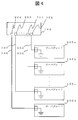
- FIG. 4 is a conceptual diagram illustrating a method in which the management module 180 recognizes the existence of the server blade 100.
- the management module 180 includes server slots 301 to 304 for inserting the server blades 100a to 100d. Each server blade and server blade slot are connected via interfaces 305 to 308, respectively. Although not shown in FIG. 4, the server blade slots 301 to 304 are connected to the backplane 120 via connectors 122.
- the management module 180 recognizes whether or not the four server blades 100a to 100d are connected to the server blade slots 301 to 304.
- this process will be described in the following (recognition process 1) to (recognition process 3).
- the management module 180 can detect that a server blade has been inserted into the corresponding server blade slot when the signal level of the interface has dropped to the ground level.
- the method for recognizing which server blade slot is inserted in the server blade has been described above.
- the management module 180 can also recognize in which slot the switch module is inserted by the same method.
- FIG. 5 is a sequence chart from when the server blade is inserted into the server blade slot to when it is activated. Hereinafter, each step of FIG. 5 will be described.
- Step S500 The user inserts a server blade into the server blade slot.
- Step S501 The management module 180 recognizes in which server blade slot the server blade is inserted using the method described in FIG.
- Step S502 When the server blade is inserted into the server blade slot, the BMC 103 is activated.
- the management module 180 reads the server blade configuration information (such as the server blade model name) inserted in step S500 via the management interface 181.
- Step S504 The nonvolatile memory element 102 outputs the server blade configuration information to the management module 180 via the management interface 181.
- Step S505 The management module 180 recognizes the type of the server blade inserted in step S500 based on the information obtained from the nonvolatile memory element 102.
- the management module 180 requests the BMC 103 to read the configuration information (such as the model name of the data communication adapter 110) of the data communication adapter 110 included in the server blade inserted in step S500 via the management interface 182.
- Step S507 The BMC 103 reads configuration information held by the nonvolatile memory element 104 via the management interface 120 or 121.
- Step S508 The nonvolatile memory element 104 outputs the held configuration information to the BMC 103 via the management interface 120 or 121.
- Step S509 Based on the information obtained from the nonvolatile memory element 104, the management module 180 recognizes the type of the data communication adapter 110 included in the server blade inserted in step S500.
- the management module 180 acquires from the server correction value table the signal correction value corresponding to the server blade type acquired in step S505 and the data communication adapter type recognized in step S509. If the server blade slot number and the server blade type have a one-to-one correspondence, specify the server blade type using the server blade slot number when specifying the corresponding signal correction value. May be. If the server blade slot number and server blade type do not correspond one-to-one, the correction value table has a “server blade type” column, a “data communication adapter type” column, etc. A corresponding signal correction value may be acquired.
- the management module 180 requests the BMC 103 to set the signal correction value acquired in step S510 in each of the signal correction elements 112 to 115 via the management interface 182.
- the BMC 103 sets the signal correction value received from the management module 180 via the management interface 120 or 121 to the nonvolatile memory element 104 or each of the signal correction elements 112 to 115.
- the signal correction elements 112 to 115 include a storage element that holds a signal correction value
- the signal correction elements 112 to 115 are directly set in the signal correction elements 112 to 115.
- a signal correction value is stored in the nonvolatile storage element 104, and the signal correction elements 112 to 115 refer to this.
- Step S513 Through the above steps, the server blade 100 is ready for startup with the signal correction value set. Thereafter, general server blade activation processing such as OS (Operating System) activation is executed.
- OS Operating System
- FIG. 6 is a sequence chart from when the switch module is inserted into a predetermined switch slot to when it is activated. Hereinafter, each step of FIG. 6 will be described.
- Step S600 The user inserts the switch module into the switch slot.
- Step S601 The management module 180 recognizes in which switch slot the switch module is inserted using the method described in FIG.
- Step S602 The management module 180 reads the configuration information (switch module model name, etc.) of the switch module inserted in step S600 via the management interface 184.
- the nonvolatile memory element (nonvolatile memory element 143 or 163 in the configuration example of FIG. 1) included in the switch module outputs the switch module configuration information to the management module 180 via the management interface 184.
- Step S604 The management module 180 recognizes the type of the switch module inserted in step S600 based on the information obtained from the nonvolatile memory element included in the switch module.
- Step S605 The management module 180 turns on the power of the switch module inserted in step S600.
- Step S606 The switch module performs a predetermined activation process.
- Step S607 The management module 180 receives a startup completion notification from the switch module. Next, the management module 180 acquires a signal correction value corresponding to the type of the switch module acquired in step S604 from the switch correction value table. If the switch slot number and the switch module type have a one-to-one correspondence, specify the switch module type using the switch slot number when specifying the corresponding signal correction value. Also good. If the switch slot number does not correspond to the switch module type on a one-to-one basis, a “switch module type” column or the like is provided in the correction value table, and a signal correction value corresponding to the recognized type is acquired. Good.
- Step S608 The management module 180 sets the signal correction value acquired in step S607 to each of the signal correction elements 142 and 162 via the management interface 184.
- the signal correction value is stored in the nonvolatile memory elements 143 and 163, and the signal correction elements 142 and 162 refer to this.
- Step S609 Through the above steps, the switch module is ready for startup with the signal correction value set.
- the data communication adapter 110 includes the dedicated signal correction elements 112 to 115 has been described. Instead, the data communication adapter 110 main body has a function of performing signal correction. It may be. In this case, the signal correction value of the data communication adapter 110 does not necessarily have to pass through the BMC 103. For example, the signal correction value setting process can be completed inside the server blade 100 via the OS of the server blade 100.
- the management module 180 can directly set the signal correction value to each data communication controller via the management interfaces 185 and 186.
- the signal correction element can be provided only in the portion corresponding to the reception port.
- Other configurations are the same as those in any of Embodiments 1 to 4.
- each data communication controller has a signal correction function
- a configuration in which each data communication controller performs correction at the time of signal transmission by itself and entrusts correction at the time of signal reception to the signal correction element is conceivable. .
- the configuration of the electronic computer 10 described in the first to fifth embodiments is particularly effective when the frequency of communication signals used by the server blade 100 and each switch module is 8 GHz or more. This is because when using a frequency of 8 GHz or more, the influence of signal deterioration tends to be prominent.
Landscapes
- Engineering & Computer Science (AREA)
- Computer Networks & Wireless Communication (AREA)
- Signal Processing (AREA)
- Power Engineering (AREA)
- Multi Processors (AREA)
Abstract
L'information concerne un ordinateur qui peut régler une valeur de correction de signal appropriée en fonction de la configuration d'un substrat connecté à un chemin commun de transmission des signaux. L'ordinateur comprend une table de valeurs de correction qui contient une valeur de correction pour la correction d'un signal transmis et reçu entre une unité de calcul et une unité de commutation pour chacun des types d'unité de calcul ou chacun des connecteurs de l'unité de calcul, et corrige le signal en utilisant la table de valeurs de correction.
Priority Applications (1)
| Application Number | Priority Date | Filing Date | Title |
|---|---|---|---|
| PCT/JP2009/061159 WO2010146699A1 (fr) | 2009-06-19 | 2009-06-19 | Ordinateur et procédé de correction d'un signal informatique |
Applications Claiming Priority (1)
| Application Number | Priority Date | Filing Date | Title |
|---|---|---|---|
| PCT/JP2009/061159 WO2010146699A1 (fr) | 2009-06-19 | 2009-06-19 | Ordinateur et procédé de correction d'un signal informatique |
Publications (1)
| Publication Number | Publication Date |
|---|---|
| WO2010146699A1 true WO2010146699A1 (fr) | 2010-12-23 |
Family
ID=43356037
Family Applications (1)
| Application Number | Title | Priority Date | Filing Date |
|---|---|---|---|
| PCT/JP2009/061159 WO2010146699A1 (fr) | 2009-06-19 | 2009-06-19 | Ordinateur et procédé de correction d'un signal informatique |
Country Status (1)
| Country | Link |
|---|---|
| WO (1) | WO2010146699A1 (fr) |
Cited By (1)
| Publication number | Priority date | Publication date | Assignee | Title |
|---|---|---|---|---|
| JP2014225850A (ja) * | 2013-05-17 | 2014-12-04 | Necプラットフォームズ株式会社 | データ伝送装置、データ伝送システム、伝送制御値の算出方法、データ伝送方法、プログラムおよび記録媒体 |
Citations (2)
| Publication number | Priority date | Publication date | Assignee | Title |
|---|---|---|---|---|
| JP2006042179A (ja) * | 2004-07-29 | 2006-02-09 | Hitachi Ltd | 記憶装置システム及び記憶装置システム内での信号伝送方法 |
| JP2007510377A (ja) * | 2003-10-27 | 2007-04-19 | ラムバス・インコーポレーテッド | 透明マルチモードpamインタフェース |
-
2009
- 2009-06-19 WO PCT/JP2009/061159 patent/WO2010146699A1/fr active Application Filing
Patent Citations (2)
| Publication number | Priority date | Publication date | Assignee | Title |
|---|---|---|---|---|
| JP2007510377A (ja) * | 2003-10-27 | 2007-04-19 | ラムバス・インコーポレーテッド | 透明マルチモードpamインタフェース |
| JP2006042179A (ja) * | 2004-07-29 | 2006-02-09 | Hitachi Ltd | 記憶装置システム及び記憶装置システム内での信号伝送方法 |
Non-Patent Citations (1)
| Title |
|---|
| "Blade Server no Kosokuka o Jitsugen suru Ta-channel Kosoku Sojushin Kairo o Kaihatsu -4 channelxlOGbps no Ko Seinoka to Tei Shohi Denryokuka ? Kogataka o Jitsugen", FUJITSU PRESS RELEASE, February 2009 (2009-02-01), Retrieved from the Internet <URL:http://pr.fujitsu.com/jp/news/2009/02/12-1.html> [retrieved on 20090910] * |
Cited By (1)
| Publication number | Priority date | Publication date | Assignee | Title |
|---|---|---|---|---|
| JP2014225850A (ja) * | 2013-05-17 | 2014-12-04 | Necプラットフォームズ株式会社 | データ伝送装置、データ伝送システム、伝送制御値の算出方法、データ伝送方法、プログラムおよび記録媒体 |
Similar Documents
| Publication | Publication Date | Title |
|---|---|---|
| CN111030778B (zh) | 高速信号的参数自适应方法、装置、设备及可读存储介质 | |
| JP4843800B2 (ja) | 信号伝送装置及び方法 | |
| US8989589B2 (en) | Method and apparatus for testing using a transceiver module | |
| KR100756745B1 (ko) | 종단저항을 이용한 can 통신 복구 시스템 | |
| EP2244191A1 (fr) | Appareil de transmission de signaux d'interconnexion de composants périphériques (PCI-E) et appareil de formation d'images l'utilisant | |
| US9722643B2 (en) | Enhanced echo cancellation in full-duplex communication | |
| EP2991234B1 (fr) | Procédé, appareil et système de configuration d'un paramètre de bus serie à grande vitesse | |
| JP5346072B2 (ja) | ユニバーサルシリアルバス(usb)システムのオンライン較正方法及びその装置 | |
| WO2010146699A1 (fr) | Ordinateur et procédé de correction d'un signal informatique | |
| US9128831B2 (en) | Electrical device and method of setting address | |
| JP4783709B2 (ja) | 信号補正量設定装置、信号補正量設定方法および信号補正量設定プログラム | |
| US9509421B2 (en) | Differential signal transmission circuit, disk array controller, and differential signal transmission cable | |
| US9667454B1 (en) | Adaptive equalizer | |
| KR101649824B1 (ko) | Emc 시험 시스템 | |
| CN203675437U (zh) | 电路板及具有此电路板的电子装置 | |
| CN102130701B (zh) | 功耗调整方法、装置及系统 | |
| US9960811B1 (en) | DC bias signals isolatable from transmission protocols | |
| CN113726425B (zh) | 一种有线通信方法、装置、设备及可读存储介质 | |
| KR102085731B1 (ko) | 배전반 결선 시험 장치 | |
| CN113407470B (zh) | 少针脚型接口和通用异步收发器接口复用方法、装置、设备 | |
| US11277297B2 (en) | Method and apparatus for multiple physical layer interfaces within a single connector | |
| KR20110079540A (ko) | 유선 직렬 통신용 송수신기 | |
| US10530500B2 (en) | Measurement system and measurement method | |
| JP2020129781A (ja) | 通信用ケーブルモジュールおよびそれを用いた通信方法 | |
| WO2015155816A1 (fr) | Dispositif de réseau et procédé de communication |
Legal Events
| Date | Code | Title | Description |
|---|---|---|---|
| 121 | Ep: the epo has been informed by wipo that ep was designated in this application |
Ref document number: 09846192 Country of ref document: EP Kind code of ref document: A1 |
|
| NENP | Non-entry into the national phase |
Ref country code: DE |
|
| 122 | Ep: pct application non-entry in european phase |
Ref document number: 09846192 Country of ref document: EP Kind code of ref document: A1 |
|
| NENP | Non-entry into the national phase |
Ref country code: JP |