WO2010146699A1 - Computer and computer signal correction method - Google Patents
Computer and computer signal correction method Download PDFInfo
- Publication number
- WO2010146699A1 WO2010146699A1 PCT/JP2009/061159 JP2009061159W WO2010146699A1 WO 2010146699 A1 WO2010146699 A1 WO 2010146699A1 JP 2009061159 W JP2009061159 W JP 2009061159W WO 2010146699 A1 WO2010146699 A1 WO 2010146699A1
- Authority
- WO
- WIPO (PCT)
- Prior art keywords
- correction value
- signal
- unit
- switch unit
- arithmetic unit
- Prior art date
Links
Images


Classifications
-
- H—ELECTRICITY
- H04—ELECTRIC COMMUNICATION TECHNIQUE
- H04L—TRANSMISSION OF DIGITAL INFORMATION, e.g. TELEGRAPHIC COMMUNICATION
- H04L25/00—Baseband systems
- H04L25/02—Details ; arrangements for supplying electrical power along data transmission lines
- H04L25/03—Shaping networks in transmitter or receiver, e.g. adaptive shaping networks
- H04L25/03878—Line equalisers; line build-out devices
-
- H—ELECTRICITY
- H04—ELECTRIC COMMUNICATION TECHNIQUE
- H04B—TRANSMISSION
- H04B3/00—Line transmission systems
- H04B3/02—Details
- H04B3/04—Control of transmission; Equalising
-
- H—ELECTRICITY
- H04—ELECTRIC COMMUNICATION TECHNIQUE
- H04L—TRANSMISSION OF DIGITAL INFORMATION, e.g. TELEGRAPHIC COMMUNICATION
- H04L25/00—Baseband systems
- H04L25/02—Details ; arrangements for supplying electrical power along data transmission lines
- H04L25/03—Shaping networks in transmitter or receiver, e.g. adaptive shaping networks
- H04L25/03006—Arrangements for removing intersymbol interference
- H04L25/03343—Arrangements at the transmitter end
Definitions
- the present invention relates to an electronic computer and a signal correction method for the electronic computer.
- Data transfer between modules in the blade server device is performed via a common signal transmission path composed of a circuit board called a backplane.
- a plurality of substrates are connected to the backplane, and data transfer is performed between the substrates.
- the signal waveform flowing on the backplane undergoes signal degradation due to waveform distortion or attenuation during the flow through the transmission line.
- Factors of signal degradation include transmission frequency, transmission distance, backplane material, transmission path conductor area, etc. Various factors combine to cause signal degradation. Among them, the factors having a particularly large influence are the transmission frequency and the transmission distance.
- the wiring length on the backplane is not necessarily constant in all transmission paths. As the wiring length becomes longer, the signal is further deteriorated, so that it is necessary to emphasize the level of signal correction. On the other hand, if an unnecessarily strong signal correction is applied to a route having a short wiring length, overcompensation occurs and the signal quality deteriorates.
- the reasons for signal degradation include various factors such as interference due to the arrangement of signal lines and the characteristics of communication adapters in addition to the wiring length.
- the present invention has been made to solve the above-described problems, and provides an electronic computer capable of setting an appropriate signal correction value according to the configuration of a substrate or the like connected to a common signal transmission path. The purpose is to obtain.
- the electronic computer includes a correction value table for holding a correction value for correcting a signal transmitted and received between the arithmetic unit and the switch unit for each type of arithmetic unit or each arithmetic unit connector, The signal is corrected using the correction value table.
- FIG. 1 is a functional block diagram of an electronic computer 10 according to a first embodiment. It is a figure which shows the structure of a correction value table with which the management module 180 is provided, and a data example.
- FIG. 10 is a diagram illustrating a configuration of a correction value table and an example of data in the second embodiment.
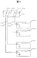
- 3 is a conceptual diagram illustrating a method for a management module 180 to recognize the presence of a server blade 100.
- FIG. 6 is a sequence chart from when a server blade is inserted into a server blade slot to when it is activated.
- 4 is a sequence chart from when a switch module is inserted into a predetermined switch slot to when it is activated.
- FIG. 1 is a functional block diagram of an electronic computer 10 according to Embodiment 1 of the present invention.
- the electronic computer 10 is a blade server device in which one or more server blades and one or more switch modules are connected via a backplane 120.
- FIG. 1 illustrates a configuration including one server blade 100 and two switch modules (first switch module 140 and second switch module 160), the number of server blades and switch modules is not limited to this. .
- the electronic computer 10 includes a server blade 100, a backplane 120, a first switch module 140, a second switch module 160, and a management module 180.
- the server blade 100, the first switch module 140, and the second switch module 160 transmit and receive serial data via the backplane 120.
- the server blade 100 includes an I / O controller 101, a nonvolatile storage element 102, a BMC (board management controller) 103, and a data communication adapter 110.
- the I / O controller 101 controls data communication processing performed by the server blade 100 with each switch module.
- the nonvolatile memory element 102 stores information representing the configuration of each functional unit included in the server blade 100. For example, in the example of FIG. 1, the model name of the server blade 100 is stored. This will be explained later.
- the BMC 103 is connected to the data communication adapter 110 via the management interfaces 120 and 121.
- the BMC 103 inputs and outputs signals between a nonvolatile memory element 104 and signal correction elements 112 to 115 described later. Details will be described later.
- the data communication adapter 110 is a communication unit used by the server blade 100 to transmit / receive a communication signal to / from each switch module via the backplane 120.
- the data communication adapter 110 includes a nonvolatile memory element 104, a data communication controller 111, and signal correction elements 112, 113, 114, and 115.
- the nonvolatile memory element 104 stores information representing the configuration of the data communication adapter 110. For example, in the example of FIG. 1, information such as the model name of the data communication adapter 110, the number of communication ports of the data communication controller 111, and the setting values of the signal correction values of the signal correction elements 112 to 115 are stored.
- the data communication controller 111 is a functional unit that controls communication processing performed by the data communication adapter 110, and includes communication ports 116, 117, 118, and 119. Each communication port is connected to a signal correction element 112, 113, 114, 115, communication ports 116 and 118 are transmission ports, and 117 and 119 are reception ports.
- the signal correction elements 112 to 115 have a function of correcting communication signals transmitted and received by the communication ports 116 to 119.
- the signal correction element 112 and the communication port 116, the signal correction element 113 and the communication port 117, the signal correction element 114 and the communication port 118, and the signal correction element 115 and the communication port 119 are respectively connected.
- the signal correction elements 112 and 114 correct the transmission signal, and 113 and 115 correct the reception signal.
- the backplane 120 has a circuit board having wiring for connecting the server blade 100 and each switch module.
- the backplane 120 includes connectors 121, 122, 123 and signal lines 124, 125, 126, 127.
- the backplane 120 and the server blade 100 are connected via a connector 122.
- the backplane 120 and the first switch module 140 are connected via a connector 121.
- the backplane 120 and the second switch module 160 are connected via a connector 123.
- Connectors 121 and 122 are connected via transmission lines 124 and 125.
- the transmission path 124 is connected to the signal correction element 112, and the transmission path 125 is connected to the signal correction element 113.
- Connectors 123 and 122 are connected via transmission lines 126 and 127.
- the transmission path 126 is connected to the signal correction element 114, and the transmission path 127 is connected to the signal correction element 115.
- the first switch module 140 is connected to the external network of the electronic computer 10.
- the server blade 100 can communicate with an external network via the first switch module 140.
- the first switch module 140 includes a data communication controller 141, a signal correction element 142, and a nonvolatile memory element 143.
- the data communication controller 141 is a functional unit that controls communication processing performed by the first switch module 140 and includes communication ports 144 and 145.
- the communication port 144 is connected to the signal correction element 142, the communication port 144 is a reception port, and 145 is a transmission port.
- the signal correction element 142 corrects the communication signal received by the communication port 144.
- the nonvolatile memory element 143 stores information representing the configuration of the first switch module 140. For example, in the example of FIG. 1, information such as the model name of the data communication controller 141, the number of communication ports, and the setting value of the signal correction value of the signal correction element 142 is stored.
- the second switch module 160 is connected to the external network of the electronic computer 10.
- the server blade 100 can communicate with an external network via the second switch module 160.
- the second switch module 160 includes a data communication controller 161, a signal correction element 162, and a nonvolatile memory element 163. These functions are the same as corresponding parts of the first switch module 140.
- the first switch module 140 and the second switch module 160 also have a role of making the connection path between the server blade 100 and the external network redundant.
- the management module 180 manages the operation of the server blade 100, the first switch module 140, and the second switch module 160.
- the management module 180 includes management interfaces 181, 182, 183, 184, 185, and 186. Further, the management module 180 includes a correction value table described later with reference to FIG. This correction value table is stored in an appropriate storage device such as a memory device.
- the management interface 181 is connected to the nonvolatile memory element 102.
- the management interface 182 is connected to the BMC 103.
- the management interface 183 is connected to the signal correction elements 142 and 162.
- the management interface 184 is connected to the nonvolatile memory elements 143 and 163.
- the management interface 185 is connected to the data communication controller 161.
- the management interface 185 is connected to the data communication controller 161.
- the management interface 186 is connected to the data communication controller 141.
- the “arithmetic unit” in the first embodiment corresponds to the server blade 100.
- the “switch unit” corresponds to each switch module.
- the “management unit” corresponds to the management module 180.
- the “common signal transmission path” corresponds to the backplane 120.
- the “arithmetic unit connector” corresponds to the connector 122.
- the “switch unit connector” corresponds to the connectors 121 and 123.
- Degradation of signal waveform is caused by various factors such as transmission line length, communication port characteristics, and interference between transmission lines. Therefore, if these configurations are different, it is necessary to individually set a correction value for performing signal correction.
- an appropriate signal correction value is obtained in advance by an experiment or the like under the configuration of a specific server blade 100 or each switch module, and this is stored in a correction value table described later.
- each signal correction element corrects the waveform of the communication signal using this correction value. Accordingly, signal correction can be appropriately performed under the configuration of a specific server blade 100 or each switch module.
- FIG. 2 is a diagram illustrating a configuration of a correction value table included in the management module 180 and an example of data.
- the correction value table has a server correction value table shown in FIG. 2A and a switch correction value table shown in FIG. Note that the values in each table are provisional.
- the server correction value table holds signal correction values for each server blade.
- signal correction values for the two server blades 100 are illustrated.
- each server blade includes one data communication adapter 110, and each data communication adapter includes four communication ports including a transmission port and a reception port.
- Port numbers 0 and 2 represent transmission ports
- port numbers 1 and 3 represent reception ports.
- Each communication port is assigned a value in the “Amplitude Value” column, “Emphasis Value” column, and “Equalize Value” column.
- Each signal correction element performs signal correction using the correction values set in these columns.
- Amplitude value column specifies the signal amplitude at the time of transmission or reception.
- the signal correction element corresponding to the transmission port amplifies the amplitude of the transmission signal to the value in this column.
- the signal correction element corresponding to the reception port amplifies the amplitude of the reception signal to the value in this column. Considering attenuation in the transmission path, a larger amplitude value is assigned to the correction value of the transmission port.
- the “emphasis value” column is a parameter used when amplifying the harmonic component of the transmission signal.
- the signal correction element corresponding to the transmission port amplifies the harmonic component of the transmission signal according to the value in this column. Since this column is for amplifying the harmonic component of the transmission signal, the value corresponding to the reception port is set to 0.0.
- “Equalize value” column is a parameter used when amplifying the harmonic component of the received signal.
- the signal correction element corresponding to the reception port amplifies the harmonic component of the reception signal according to the value in this column. Since this column is for amplifying the harmonic component of the received signal, the value corresponding to the transmission port is set to zero.
- FIG. 2A shows an example of data assuming that each server blade includes one data communication adapter 110.
- each server blade includes a plurality of data communication adapters 110, a column indicating the number of the data communication adapter 110 and the like is separately provided in the server correction value table, and each data communication adapter 110 is shown in FIG. It is good to keep similar data.
- each switch module includes one data communication controller (141 or 161), and each data communication controller includes two communication ports including a transmission port and a reception port.
- Each data communication controller includes two communication ports including a transmission port and a reception port.
- An example of data was shown.
- Port number 0 represents a transmission port
- port number 1 represents a reception port.
- the meaning of the value in each column in FIG. 2B is the same as that in FIG.
- FIG. 2B shows an example of data assuming that signal correction elements are provided in both the transmission port and the reception port. However, as shown in the configuration example of FIG. If provided, only the correction value corresponding to the reception port may be held.
- FIG. 2B shows an example of data assuming that each switch module has one data communication controller.
- each switch module includes a plurality of data communication controllers, a column indicating the number of the data communication controller is separately provided in the switch correction value table, and the same data as in FIG. It is good to keep.
- Step 1 Obtaining a correction value from the server correction value table
- the management module 180 obtains a signal correction value for each communication port included in the data communication adapter of each server blade from the server correction value table described in FIG. get.
- Step 2 Outputting the correction value to the BMC 103
- the management module 180 outputs the correction value acquired in Step 1 to the BMC 103 via the management interface 182.
- Step 3 Setting Correction Values in Each Signal Correction Element
- the BMC 103 sets the signal correction values received from the management module 180 in each signal correction element 112-115.
- Each of the signal correction elements 112 to 115 stores the signal correction value in a storage element or the like provided therein.
- the management module 180 may store the signal correction value of the signal correction element in the nonvolatile storage element 104.
- Step 4 Obtaining a correction value from the switch correction value table
- the management module 180 obtains a signal correction value for each communication port included in the data communication controller of each switch module from the switch correction value table described in FIG. get.
- Step 5 Output Correction Value
- the management module 180 outputs the correction value acquired in step 4 to each signal correction element (142 and 162) via the management interface 183.
- the management module 180 may store the signal correction value of the signal correction element in the nonvolatile storage element 143.
- Each signal correction element corrects the transmission signal and the reception signal using the signal correction value set by the management module 180.
- the management module 180 includes the server correction value table that holds the signal correction value for each server blade 100, and data communication of each server blade 100 using the correction value.
- the signal correction value of the adapter 110 is set.
- Each of the signal correction elements 112 to 115 included in the data communication adapter 110 corrects the communication signal using the signal correction value.
- the management module 180 includes a switch correction value table that holds a signal correction value for each switch module, and the correction value is used for the signal correction value of the data communication controller of each switch module. Set. Each signal correction element included in the data communication controller corrects the communication signal using the signal correction value.
- the server correction value table and the switch correction value table hold the signal correction value for each communication port included in each data communication controller.
- the signal correction value can be set in detail, more appropriate signal correction can be performed as compared with the case where the signal correction value is set for each server blade or each switch module.
- the signal correction value can be set according to the type of the transmission port / reception port, the accuracy of signal correction is improved.
- An electronic computer such as a blade server device is configured to be able to change a signal frequency by replacing a server blade, a switch module, or a component of these with a compatible module having a different communication frequency. There is a case. If the communication frequency is different, the characteristics of signal degradation change, so using the same signal correction value as before changing the frequency may result in overcompensation or insufficient correction.
- the management module 180 includes a correction value table for each signal frequency used by the server blade 100 or the switch module, and performs signal correction according to the signal frequency. Since the configuration other than the correction value table is substantially the same as that of the first embodiment, the following description focuses on the differences.
- the computer 10 has, for example, any one of the following (Configuration Example 1) to (Configuration Example 3), and is configured to be able to change the frequency of a communication signal. .
- the data communication controllers 111, 141, 142 are configured to be able to change the frequency of communication signals to be used.
- the server blade 100 or each switch module is configured so that the data communication controller can be replaced with a compatible controller having a different frequency of communication signals.
- each data communication controller is configured to be exchangeable with compatible components having different frequencies of communication signals to be used.
- the management module 180 can specify the frequency of the communication signal used by each data communication controller.
- the frequency of the communication signal used by each data communication controller is stored as setting information in the nonvolatile memory elements 104, 143, 163, etc., respectively, and the management module 180 reads this to acquire the setting value of the frequency Shall be able to.
- the management module 180 reads the type of each data communication controller from the nonvolatile memory elements 104, 143, 163, etc., and specifies the frequency corresponding to the type.
- FIG. 3 is a diagram showing a configuration of a correction value table and a data example in the second embodiment.
- a correction value table is provided for each frequency of communication signals used by the server blade 100 and each switch module.
- FIGS. 3A and 3B are tables holding respective correction values when the frequency of the communication signal is 8 GHz
- FIGS. 3C and 3D show the correction values when the frequency of the communication signal is 4 GHz. It is a table to hold. It should be noted that each piece of data shown in FIG. 3 is an example.
- Step 1 Obtaining the frequency of the communication signal
- the management module 180 obtains the frequency of the communication signal used by the data communication controller included in the server blade 100 and each switch module from the nonvolatile memory elements 104, 143, and 163.
- Step 2 Acquiring Correction Value from Server Correction Value Table
- the management module 180 acquires a signal correction value for each communication port included in the data communication adapter of each server blade from the server correction value table described with reference to FIG. At this time, the management module 180 acquires the signal correction value from the server correction value table corresponding to the frequency of the data communication adapter 111 acquired in step 1.
- Step 3 Setting correction values in each signal correction element
- Step 5 Acquiring Correction Value from Switch Correction Value Table
- the management module 180 acquires a signal correction value for each communication port included in the data communication controller of each switch module from the switch correction value table described with reference to FIG. At this time, the management module 180 acquires the signal correction value from the server correction value table corresponding to the frequencies of the data communication adapters 142 and 162 acquired in step 1.
- Step 6 Output Correction Value This step is the same as Step 5 described in the first embodiment.
- the correction value table holds the signal correction value of the communication port of each server blade and each switch module for each frequency of the communication signal used by each data communication controller. ing.
- the management module 180 can set an appropriate signal correction value even when the frequency of the communication signal changes and the signal degradation characteristic changes, so that the data transfer quality can be improved regardless of the frequency of the communication signal. Can be improved.
- FIG. 4 is a conceptual diagram illustrating a method in which the management module 180 recognizes the existence of the server blade 100.
- the management module 180 includes server slots 301 to 304 for inserting the server blades 100a to 100d. Each server blade and server blade slot are connected via interfaces 305 to 308, respectively. Although not shown in FIG. 4, the server blade slots 301 to 304 are connected to the backplane 120 via connectors 122.
- the management module 180 recognizes whether or not the four server blades 100a to 100d are connected to the server blade slots 301 to 304.
- this process will be described in the following (recognition process 1) to (recognition process 3).
- the management module 180 can detect that a server blade has been inserted into the corresponding server blade slot when the signal level of the interface has dropped to the ground level.
- the method for recognizing which server blade slot is inserted in the server blade has been described above.
- the management module 180 can also recognize in which slot the switch module is inserted by the same method.
- FIG. 5 is a sequence chart from when the server blade is inserted into the server blade slot to when it is activated. Hereinafter, each step of FIG. 5 will be described.
- Step S500 The user inserts a server blade into the server blade slot.
- Step S501 The management module 180 recognizes in which server blade slot the server blade is inserted using the method described in FIG.
- Step S502 When the server blade is inserted into the server blade slot, the BMC 103 is activated.
- the management module 180 reads the server blade configuration information (such as the server blade model name) inserted in step S500 via the management interface 181.
- Step S504 The nonvolatile memory element 102 outputs the server blade configuration information to the management module 180 via the management interface 181.
- Step S505 The management module 180 recognizes the type of the server blade inserted in step S500 based on the information obtained from the nonvolatile memory element 102.
- the management module 180 requests the BMC 103 to read the configuration information (such as the model name of the data communication adapter 110) of the data communication adapter 110 included in the server blade inserted in step S500 via the management interface 182.
- Step S507 The BMC 103 reads configuration information held by the nonvolatile memory element 104 via the management interface 120 or 121.
- Step S508 The nonvolatile memory element 104 outputs the held configuration information to the BMC 103 via the management interface 120 or 121.
- Step S509 Based on the information obtained from the nonvolatile memory element 104, the management module 180 recognizes the type of the data communication adapter 110 included in the server blade inserted in step S500.
- the management module 180 acquires from the server correction value table the signal correction value corresponding to the server blade type acquired in step S505 and the data communication adapter type recognized in step S509. If the server blade slot number and the server blade type have a one-to-one correspondence, specify the server blade type using the server blade slot number when specifying the corresponding signal correction value. May be. If the server blade slot number and server blade type do not correspond one-to-one, the correction value table has a “server blade type” column, a “data communication adapter type” column, etc. A corresponding signal correction value may be acquired.
- the management module 180 requests the BMC 103 to set the signal correction value acquired in step S510 in each of the signal correction elements 112 to 115 via the management interface 182.
- the BMC 103 sets the signal correction value received from the management module 180 via the management interface 120 or 121 to the nonvolatile memory element 104 or each of the signal correction elements 112 to 115.
- the signal correction elements 112 to 115 include a storage element that holds a signal correction value
- the signal correction elements 112 to 115 are directly set in the signal correction elements 112 to 115.
- a signal correction value is stored in the nonvolatile storage element 104, and the signal correction elements 112 to 115 refer to this.
- Step S513 Through the above steps, the server blade 100 is ready for startup with the signal correction value set. Thereafter, general server blade activation processing such as OS (Operating System) activation is executed.
- OS Operating System
- FIG. 6 is a sequence chart from when the switch module is inserted into a predetermined switch slot to when it is activated. Hereinafter, each step of FIG. 6 will be described.
- Step S600 The user inserts the switch module into the switch slot.
- Step S601 The management module 180 recognizes in which switch slot the switch module is inserted using the method described in FIG.
- Step S602 The management module 180 reads the configuration information (switch module model name, etc.) of the switch module inserted in step S600 via the management interface 184.
- the nonvolatile memory element (nonvolatile memory element 143 or 163 in the configuration example of FIG. 1) included in the switch module outputs the switch module configuration information to the management module 180 via the management interface 184.
- Step S604 The management module 180 recognizes the type of the switch module inserted in step S600 based on the information obtained from the nonvolatile memory element included in the switch module.
- Step S605 The management module 180 turns on the power of the switch module inserted in step S600.
- Step S606 The switch module performs a predetermined activation process.
- Step S607 The management module 180 receives a startup completion notification from the switch module. Next, the management module 180 acquires a signal correction value corresponding to the type of the switch module acquired in step S604 from the switch correction value table. If the switch slot number and the switch module type have a one-to-one correspondence, specify the switch module type using the switch slot number when specifying the corresponding signal correction value. Also good. If the switch slot number does not correspond to the switch module type on a one-to-one basis, a “switch module type” column or the like is provided in the correction value table, and a signal correction value corresponding to the recognized type is acquired. Good.
- Step S608 The management module 180 sets the signal correction value acquired in step S607 to each of the signal correction elements 142 and 162 via the management interface 184.
- the signal correction value is stored in the nonvolatile memory elements 143 and 163, and the signal correction elements 142 and 162 refer to this.
- Step S609 Through the above steps, the switch module is ready for startup with the signal correction value set.
- the data communication adapter 110 includes the dedicated signal correction elements 112 to 115 has been described. Instead, the data communication adapter 110 main body has a function of performing signal correction. It may be. In this case, the signal correction value of the data communication adapter 110 does not necessarily have to pass through the BMC 103. For example, the signal correction value setting process can be completed inside the server blade 100 via the OS of the server blade 100.
- the management module 180 can directly set the signal correction value to each data communication controller via the management interfaces 185 and 186.
- the signal correction element can be provided only in the portion corresponding to the reception port.
- Other configurations are the same as those in any of Embodiments 1 to 4.
- each data communication controller has a signal correction function
- a configuration in which each data communication controller performs correction at the time of signal transmission by itself and entrusts correction at the time of signal reception to the signal correction element is conceivable. .
- the configuration of the electronic computer 10 described in the first to fifth embodiments is particularly effective when the frequency of communication signals used by the server blade 100 and each switch module is 8 GHz or more. This is because when using a frequency of 8 GHz or more, the influence of signal deterioration tends to be prominent.
Abstract
Provided is a computer which can set an appropriate signal correction value in accordance with configuration of a substrate connected to a common signal transmission path.
The computer includes a correction value table which holds a correction value for correcting a signal transmitted and received between a calculation unit and a switch unit for each of the calculation unit types or each of the calculation unit connectors and corrects the signal by using the correction value table.
Description
本発明は、電子計算機および電子計算機の信号補正方法に関するものである。
The present invention relates to an electronic computer and a signal correction method for the electronic computer.
ブレードサーバ装置内のモジュール間のデータ転送は、バックプレーンと呼ばれる回路基板からなる共通信号伝送路を介して行われる。バックプレーンには複数の基板が接続され、それら基板間でデータ転送を行う。このとき、バックプレーン上を流れる信号の波形には、伝送路を流れる途中で、波形の歪みや減衰による信号劣化が生じる。
Data transfer between modules in the blade server device is performed via a common signal transmission path composed of a circuit board called a backplane. A plurality of substrates are connected to the backplane, and data transfer is performed between the substrates. At this time, the signal waveform flowing on the backplane undergoes signal degradation due to waveform distortion or attenuation during the flow through the transmission line.
この信号劣化を解決するためには、伝送波形に補正をかけ波形状態を改善させる処理を行うことが考えられる。信号の処理には、さまざまな手法が考え出されている。中でも、伝送路中の波形の減衰を予想し、送信側であらかじめ減衰分を増幅してから送信する技術や、伝送中に弱まった波形を受信側で復元させる技術が一般的に用いられている。上記技術の例として、下記特許文献1がある。
In order to solve this signal degradation, it is conceivable to correct the transmission waveform and improve the waveform state. Various techniques have been devised for signal processing. In particular, a technique for predicting the attenuation of the waveform in the transmission path and amplifying the attenuation in advance on the transmission side, and a technique for restoring a waveform weakened during transmission on the reception side are generally used. . There exists following patent document 1 as an example of the said technique.
信号劣化の要因は、伝送周波数や伝送距離、バックプレーンの材質、伝送路の導体面積等があり、様々な要因が複合的に合わさって信号劣化が生じる。中でも特に影響の大きい要因は、伝送周波数と伝送距離である。
Factors of signal degradation include transmission frequency, transmission distance, backplane material, transmission path conductor area, etc. Various factors combine to cause signal degradation. Among them, the factors having a particularly large influence are the transmission frequency and the transmission distance.
ブレードサーバ装置では、複数の基板がバックプレーンを介してデータ転送を行うため、バックプレーン上の配線長はすべての伝送経路で必ずしも一定ではない。配線長が長くなれば、より信号が劣化するため、信号補正のレベルも強調する必要がある。一方で、配線長が短い経路に対して不必要に強い信号補正を加えると、過補償となり信号品質は悪くなってしまう。
In a blade server device, since a plurality of boards transfer data via a backplane, the wiring length on the backplane is not necessarily constant in all transmission paths. As the wiring length becomes longer, the signal is further deteriorated, so that it is necessary to emphasize the level of signal correction. On the other hand, if an unnecessarily strong signal correction is applied to a route having a short wiring length, overcompensation occurs and the signal quality deteriorates.
信号劣化の原因となる理由として、配線長の他に、信号線等の配置に起因する干渉、通信アダプタの特性など、様々なものが考えられる。
The reasons for signal degradation include various factors such as interference due to the arrangement of signal lines and the characteristics of communication adapters in addition to the wiring length.
本発明は、上記のような課題を解決するためになされたものであり、共通信号伝送路に接続された基板などの構成に応じて、適切な信号補正値を設定することのできる電子計算機を得ることを目的とする。
The present invention has been made to solve the above-described problems, and provides an electronic computer capable of setting an appropriate signal correction value according to the configuration of a substrate or the like connected to a common signal transmission path. The purpose is to obtain.
本発明に係る電子計算機は、演算ユニットとスイッチユニットの間で送受信される信号を補正するための補正値を前記演算ユニットの種別毎または演算ユニットコネクタ毎に保持する補正値テーブルを備えており、その補正値テーブルを用いて前記信号を補正するものである。
The electronic computer according to the present invention includes a correction value table for holding a correction value for correcting a signal transmitted and received between the arithmetic unit and the switch unit for each type of arithmetic unit or each arithmetic unit connector, The signal is corrected using the correction value table.
本発明に係る電子計算機によれば、演算ユニット毎に補正値が設定されているので、各ユニットの特性や配置に応じた適切な補正値を用いて信号補正を行い、高品質なデータ転送を行うことができる。
According to the electronic computer of the present invention, since a correction value is set for each arithmetic unit, signal correction is performed using an appropriate correction value according to the characteristics and arrangement of each unit, and high-quality data transfer is performed. It can be carried out.
(実施の形態1)
図1は、本発明の実施の形態1に係る電子計算機10の機能ブロック図である。電子計算機10は、1以上のサーバブレードと1以上のスイッチモジュールがバックプレーン120を介して接続されるブレードサーバ装置である。 (Embodiment 1)
FIG. 1 is a functional block diagram of anelectronic computer 10 according to Embodiment 1 of the present invention. The electronic computer 10 is a blade server device in which one or more server blades and one or more switch modules are connected via a backplane 120.
図1は、本発明の実施の形態1に係る電子計算機10の機能ブロック図である。電子計算機10は、1以上のサーバブレードと1以上のスイッチモジュールがバックプレーン120を介して接続されるブレードサーバ装置である。 (Embodiment 1)
FIG. 1 is a functional block diagram of an
図1では、1つのサーバブレード100と2つのスイッチモジュール(第1スイッチモジュール140、第2スイッチモジュール160)を備える構成を図示したが、サーバブレードとスイッチモジュールの個数はこれに限られるものではない。
Although FIG. 1 illustrates a configuration including one server blade 100 and two switch modules (first switch module 140 and second switch module 160), the number of server blades and switch modules is not limited to this. .
図1において、電子計算機10は、サーバブレード100、バックプレーン120、第1スイッチモジュール140、第2スイッチモジュール160、管理モジュール180を備える。サーバブレード100、第1スイッチモジュール140、第2スイッチモジュール160は、バックプレーン120を介してシリアルデータを送受信する。
1, the electronic computer 10 includes a server blade 100, a backplane 120, a first switch module 140, a second switch module 160, and a management module 180. The server blade 100, the first switch module 140, and the second switch module 160 transmit and receive serial data via the backplane 120.
サーバブレード100は、I/Oコントローラ101、不揮発記憶素子102、BMC(ボードマネジメントコントローラ)103、データ通信アダプタ110を備える。
The server blade 100 includes an I / O controller 101, a nonvolatile storage element 102, a BMC (board management controller) 103, and a data communication adapter 110.
I/Oコントローラ101は、サーバブレード100が各スイッチモジュールとの間で行うデータ通信処理を制御する。
The I / O controller 101 controls data communication processing performed by the server blade 100 with each switch module.
不揮発記憶素子102は、サーバブレード100が備える各機能部の構成を表す情報を格納する。例えば図1の例では、サーバブレード100の機種名等を格納する。これについては後に改めて説明する。
The nonvolatile memory element 102 stores information representing the configuration of each functional unit included in the server blade 100. For example, in the example of FIG. 1, the model name of the server blade 100 is stored. This will be explained later.
BMC103は、管理用インターフェース120および121を介してデータ通信アダプタ110に接続されている。BMC103は、後述する不揮発記憶素子104および信号補正素子112~115との間で信号を入出力する。詳細は後述する。
The BMC 103 is connected to the data communication adapter 110 via the management interfaces 120 and 121. The BMC 103 inputs and outputs signals between a nonvolatile memory element 104 and signal correction elements 112 to 115 described later. Details will be described later.
データ通信アダプタ110は、サーバブレード100がバックプレーン120を介して各スイッチモジュールとの間で通信信号を送受信するために用いる通信部である。データ通信アダプタ110は、不揮発記憶素子104、データ通信コントローラ111、信号補正素子112、113、114、115を備える。
The data communication adapter 110 is a communication unit used by the server blade 100 to transmit / receive a communication signal to / from each switch module via the backplane 120. The data communication adapter 110 includes a nonvolatile memory element 104, a data communication controller 111, and signal correction elements 112, 113, 114, and 115.
不揮発記憶素子104は、データ通信アダプタ110の構成を表す情報を格納する。例えば図1の例では、データ通信アダプタ110の機種名、データ通信コントローラ111の通信ポートの数、信号補正素子112~115の信号補正値の設定値などの情報を格納する。
The nonvolatile memory element 104 stores information representing the configuration of the data communication adapter 110. For example, in the example of FIG. 1, information such as the model name of the data communication adapter 110, the number of communication ports of the data communication controller 111, and the setting values of the signal correction values of the signal correction elements 112 to 115 are stored.
データ通信コントローラ111は、データ通信アダプタ110が行う通信処理を制御する機能部であり、通信ポート116、117、118、119を備える。各通信ポートはそれぞれ、信号補正素子112、113、114、115と接続されている、通信ポート116と118は送信ポート、117と119は受信ポートである。
The data communication controller 111 is a functional unit that controls communication processing performed by the data communication adapter 110, and includes communication ports 116, 117, 118, and 119. Each communication port is connected to a signal correction element 112, 113, 114, 115, communication ports 116 and 118 are transmission ports, and 117 and 119 are reception ports.
信号補正素子112~115は、通信ポート116~119が送受信する通信信号を補正する機能を備える。信号補正素子112と通信ポート116、信号補正素子113と通信ポート117、信号補正素子114と通信ポート118、信号補正素子115と通信ポート119が、それぞれ接続されている。信号補正素子112と114は送信信号、113と115は受信信号を補正する。
The signal correction elements 112 to 115 have a function of correcting communication signals transmitted and received by the communication ports 116 to 119. The signal correction element 112 and the communication port 116, the signal correction element 113 and the communication port 117, the signal correction element 114 and the communication port 118, and the signal correction element 115 and the communication port 119 are respectively connected. The signal correction elements 112 and 114 correct the transmission signal, and 113 and 115 correct the reception signal.
バックプレーン120は、サーバブレード100と各スイッチモジュールを接続する配線を備える回路基板を有する。バックプレーン120は、コネクタ121、122、123と、信号線124、125、126、127を備える。
The backplane 120 has a circuit board having wiring for connecting the server blade 100 and each switch module. The backplane 120 includes connectors 121, 122, 123 and signal lines 124, 125, 126, 127.
バックプレーン120とサーバブレード100は、コネクタ122を介して接続されている。バックプレーン120と第1スイッチモジュール140は、コネクタ121を介して接続されている。バックプレーン120と第2スイッチモジュール160は、コネクタ123を介して接続されている。
The backplane 120 and the server blade 100 are connected via a connector 122. The backplane 120 and the first switch module 140 are connected via a connector 121. The backplane 120 and the second switch module 160 are connected via a connector 123.
コネクタ121と122は、伝送路124と125を介して接続されている。伝送路124は信号補正素子112と接続され、伝送路125は信号補正素子113と接続されている。
Connectors 121 and 122 are connected via transmission lines 124 and 125. The transmission path 124 is connected to the signal correction element 112, and the transmission path 125 is connected to the signal correction element 113.
コネクタ123と122は、伝送路126と127を介して接続されている。伝送路126は信号補正素子114と接続され、伝送路127は信号補正素子115と接続されている。
Connectors 123 and 122 are connected via transmission lines 126 and 127. The transmission path 126 is connected to the signal correction element 114, and the transmission path 127 is connected to the signal correction element 115.
第1スイッチモジュール140は、電子計算機10の外部ネットワークと接続されている。サーバブレード100は、第1スイッチモジュール140を介して外部ネットワークと通信することができる。第1スイッチモジュール140は、データ通信コントローラ141、信号補正素子142、不揮発記憶素子143を備える。
The first switch module 140 is connected to the external network of the electronic computer 10. The server blade 100 can communicate with an external network via the first switch module 140. The first switch module 140 includes a data communication controller 141, a signal correction element 142, and a nonvolatile memory element 143.
データ通信コントローラ141は、第1スイッチモジュール140が行う通信処理を制御する機能部であり、通信ポート144、145を備える。通信ポート144は、信号補正素子142と接続されている、通信ポート144は受信ポート、145は送信ポートである。
The data communication controller 141 is a functional unit that controls communication processing performed by the first switch module 140 and includes communication ports 144 and 145. The communication port 144 is connected to the signal correction element 142, the communication port 144 is a reception port, and 145 is a transmission port.
信号補正素子142は、通信ポート144が受信する通信信号を補正する。
The signal correction element 142 corrects the communication signal received by the communication port 144.
不揮発記憶素子143は、第1スイッチモジュール140の構成を表す情報を格納する。例えば図1の例では、データ通信コントローラ141の機種名、通信ポートの数、信号補正素子142の信号補正値の設定値などの情報を格納する。
The nonvolatile memory element 143 stores information representing the configuration of the first switch module 140. For example, in the example of FIG. 1, information such as the model name of the data communication controller 141, the number of communication ports, and the setting value of the signal correction value of the signal correction element 142 is stored.
第2スイッチモジュール160は、電子計算機10の外部ネットワークと接続されている。サーバブレード100は、第2スイッチモジュール160を介して外部ネットワークと通信することができる。第2スイッチモジュール160は、データ通信コントローラ161、信号補正素子162、不揮発記憶素子163を備える。これらの機能は、第1スイッチモジュール140の対応する各部と同様である。第1スイッチモジュール140と第2スイッチモジュール160は、サーバブレード100と外部ネットワークとの接続経路を冗長化する役割も有する。
The second switch module 160 is connected to the external network of the electronic computer 10. The server blade 100 can communicate with an external network via the second switch module 160. The second switch module 160 includes a data communication controller 161, a signal correction element 162, and a nonvolatile memory element 163. These functions are the same as corresponding parts of the first switch module 140. The first switch module 140 and the second switch module 160 also have a role of making the connection path between the server blade 100 and the external network redundant.
管理モジュール180は、サーバブレード100、第1スイッチモジュール140、第2スイッチモジュール160の動作を管理する。管理モジュール180は、管理用インターフェース181、182、183、184、185、186を有する。また、管理モジュール180は、後述の図2で説明する補正値テーブルを備える。この補正値テーブルはメモリ装置などの適当な記憶装置内に格納される。
The management module 180 manages the operation of the server blade 100, the first switch module 140, and the second switch module 160. The management module 180 includes management interfaces 181, 182, 183, 184, 185, and 186. Further, the management module 180 includes a correction value table described later with reference to FIG. This correction value table is stored in an appropriate storage device such as a memory device.
管理用インターフェース181は、不揮発記憶素子102と接続されている。管理用インターフェース182は、BMC103と接続されている。管理用インターフェース183は、信号補正素子142および162と接続されている。管理用インターフェース184は、不揮発記憶素子143および163と接続されている。管理用インターフェース185は、データ通信コントローラ161に接続されている。管理用インターフェース185は、データ通信コントローラ161に接続されている。管理用インターフェース186は、データ通信コントローラ141に接続されている。
The management interface 181 is connected to the nonvolatile memory element 102. The management interface 182 is connected to the BMC 103. The management interface 183 is connected to the signal correction elements 142 and 162. The management interface 184 is connected to the nonvolatile memory elements 143 and 163. The management interface 185 is connected to the data communication controller 161. The management interface 185 is connected to the data communication controller 161. The management interface 186 is connected to the data communication controller 141.
本実施の形態1における「演算ユニット」は、サーバブレード100が相当する。「スイッチユニット」は、各スイッチモジュールが相当する。「管理ユニット」は、管理モジュール180が相当する。「共通信号伝送路」は、バックプレーン120が相当する。「演算ユニットコネクタ」は、コネクタ122が相当する。「スイッチユニットコネクタ」は、コネクタ121と123が相当する。
The “arithmetic unit” in the first embodiment corresponds to the server blade 100. The “switch unit” corresponds to each switch module. The “management unit” corresponds to the management module 180. The “common signal transmission path” corresponds to the backplane 120. The “arithmetic unit connector” corresponds to the connector 122. The “switch unit connector” corresponds to the connectors 121 and 123.
以上、本実施の形態1に係る電子計算機10の構成について説明した。次に、通信信号の補正について説明する。
The configuration of the electronic computer 10 according to the first embodiment has been described above. Next, communication signal correction will be described.
一般に、ブレードサーバ装置のバックプレーンを介してデータ転送を行う場合、特に周波数の高い通信信号を用いる場合には、上述のような信号劣化が生じやすい。そのため、送信側と受信側の少なくともいずれかで信号波形を補正する必要がある。
Generally, when data is transferred via a backplane of a blade server device, particularly when a communication signal having a high frequency is used, the above-described signal deterioration is likely to occur. Therefore, it is necessary to correct the signal waveform on at least one of the transmission side and the reception side.
信号波形の劣化は、伝送路の線長、通信ポートの特性、伝送路間の干渉など、様々な要因によって生じる。そのため、これらの構成が異なれば、信号補正を行うための補正値も個別に設定する必要がある。
Degradation of signal waveform is caused by various factors such as transmission line length, communication port characteristics, and interference between transmission lines. Therefore, if these configurations are different, it is necessary to individually set a correction value for performing signal correction.
本実施の形態1では、ある特定のサーバブレード100や各スイッチモジュールの構成の下で、適切な信号補正値をあらかじめ実験などにより求めておき、これを後述の補正値テーブルに保持させておく。サーバブレード100や各スイッチモジュールがデータ転送を行う際には、各信号補正素子がこの補正値を用いて通信信号の波形を補正する。これにより、ある特定のサーバブレード100や各スイッチモジュールの構成の下で、信号補正を適切に行うことができる。
In the first embodiment, an appropriate signal correction value is obtained in advance by an experiment or the like under the configuration of a specific server blade 100 or each switch module, and this is stored in a correction value table described later. When the server blade 100 or each switch module performs data transfer, each signal correction element corrects the waveform of the communication signal using this correction value. Accordingly, signal correction can be appropriately performed under the configuration of a specific server blade 100 or each switch module.
図2は、管理モジュール180が備える補正値テーブルの構成とデータ例を示す図である。補正値テーブルは、図2(a)に示すサーバ補正値テーブルと、図2(b)に示すスイッチ補正値テーブルとを有する。なお、各テーブル中の値は仮のものである。
FIG. 2 is a diagram illustrating a configuration of a correction value table included in the management module 180 and an example of data. The correction value table has a server correction value table shown in FIG. 2A and a switch correction value table shown in FIG. Note that the values in each table are provisional.
サーバ補正値テーブルは、サーバブレード毎の信号補正値を保持している。ここでは電子計算機10が2つのサーバブレードスロットを備えている場合のデータ例として、2つのサーバブレード100それぞれについての信号補正値を例示した。
The server correction value table holds signal correction values for each server blade. Here, as a data example when the electronic computer 10 includes two server blade slots, signal correction values for the two server blades 100 are illustrated.
図2(a)のデータ例では、各サーバブレードが1つのデータ通信アダプタ110を備えており、各データ通信アダプタは送信ポートと受信ポートを合わせて4つの通信ポートを備えている場合のデータ例を示した。ポート番号0と2は送信ポート、ポート番号1と3は受信ポートを表している。
In the data example of FIG. 2A, each server blade includes one data communication adapter 110, and each data communication adapter includes four communication ports including a transmission port and a reception port. showed that. Port numbers 0 and 2 represent transmission ports, and port numbers 1 and 3 represent reception ports.
各通信ポートには、「振幅値」列、「エンファシス値」列、「イコライズ値」列の値が割り当てられている。各信号補正素子は、これらの列にセットされている補正値を用いて信号補正を行う。
Each communication port is assigned a value in the “Amplitude Value” column, “Emphasis Value” column, and “Equalize Value” column. Each signal correction element performs signal correction using the correction values set in these columns.
「振幅値」列は、送信時または受信時の信号振幅を指定する。送信ポートに対応する信号補正素子は、送信信号の振幅を本列の値まで増幅させる。受信ポートに対応する信号補正素子は、受信信号の振幅を本列の値まで増幅させる。伝送路における減衰を考慮して、送信ポートの補正値には大きめの振幅値が割り当てられる。
“Amplitude value” column specifies the signal amplitude at the time of transmission or reception. The signal correction element corresponding to the transmission port amplifies the amplitude of the transmission signal to the value in this column. The signal correction element corresponding to the reception port amplifies the amplitude of the reception signal to the value in this column. Considering attenuation in the transmission path, a larger amplitude value is assigned to the correction value of the transmission port.
「エンファシス値」列は、送信信号の高調波成分を増幅する際に用いるパラメータである。送信ポートに対応する信号補正素子は、送信信号の高調波成分を本列の値に準じて増幅させる。本列は送信信号の高調波成分を増幅させるためのものであるため、受信ポートに対応する値は0.0とした。
The “emphasis value” column is a parameter used when amplifying the harmonic component of the transmission signal. The signal correction element corresponding to the transmission port amplifies the harmonic component of the transmission signal according to the value in this column. Since this column is for amplifying the harmonic component of the transmission signal, the value corresponding to the reception port is set to 0.0.
「イコライズ値」列は、受信信号の高調波成分を増幅する際に用いるパラメータである。受信ポートに対応する信号補正素子は、受信信号の高調波成分を本列の値に準じて増幅させる。本列は受信信号の高調波成分を増幅させるためのものであるため、送信ポートに対応する値は0とした。
“Equalize value” column is a parameter used when amplifying the harmonic component of the received signal. The signal correction element corresponding to the reception port amplifies the harmonic component of the reception signal according to the value in this column. Since this column is for amplifying the harmonic component of the received signal, the value corresponding to the transmission port is set to zero.
図2(a)では、各サーバブレードが1つのデータ通信アダプタ110を備えていることを想定したデータ例を示した。各サーバブレードが複数のデータ通信アダプタ110を備えている場合には、サーバ補正値テーブル内にデータ通信アダプタ110の番号等を表す列を別途設け、各データ通信アダプタ110について図2(a)と同様のデータを保持しておくとよい。
FIG. 2A shows an example of data assuming that each server blade includes one data communication adapter 110. When each server blade includes a plurality of data communication adapters 110, a column indicating the number of the data communication adapter 110 and the like is separately provided in the server correction value table, and each data communication adapter 110 is shown in FIG. It is good to keep similar data.
図2(b)のデータ例では、各スイッチモジュールが1つのデータ通信コントローラ(141または161)を備えおり、各データ通信コントローラは送信ポートと受信ポートを合わせて2つの通信ポートを備えている場合のデータ例を示した。ポート番号0は送信ポート、ポート番号1は受信ポートを表している。図2(b)の各列の値の意味は、図2(a)と同様である。
In the data example of FIG. 2B, each switch module includes one data communication controller (141 or 161), and each data communication controller includes two communication ports including a transmission port and a reception port. An example of data was shown. Port number 0 represents a transmission port, and port number 1 represents a reception port. The meaning of the value in each column in FIG. 2B is the same as that in FIG.
なお、図2(b)では送信ポートと受信ポートの双方に信号補正素子が設けられていることを想定したデータ例を示したが、図1の構成例のように受信ポートのみ信号補正素子を備えている場合は、受信ポートに対応する補正値のみ保持するようにしてもよい。
FIG. 2B shows an example of data assuming that signal correction elements are provided in both the transmission port and the reception port. However, as shown in the configuration example of FIG. If provided, only the correction value corresponding to the reception port may be held.
また、図2(b)では、各スイッチモジュールが1つのデータ通信コントローラを備えていることを想定したデータ例を示した。各スイッチモジュールが複数のデータ通信コントローラを備えている場合には、スイッチ補正値テーブル内にデータ通信コントローラの番号等を表す列を別途設け、各データ通信コントローラについて図2(b)と同様のデータを保持しておくとよい。
Further, FIG. 2B shows an example of data assuming that each switch module has one data communication controller. When each switch module includes a plurality of data communication controllers, a column indicating the number of the data communication controller is separately provided in the switch correction value table, and the same data as in FIG. It is good to keep.
以上、補正値テーブルの構成とデータ例について説明した、次に、管理モジュール180が補正値テーブルを用いて各信号補正素子の信号補正値をセットする手順を、下記(ステップ1)~(ステップ5)で説明する。
The configuration and data example of the correction value table have been described above. Next, the procedure in which the management module 180 sets the signal correction value of each signal correction element using the correction value table is described below (Step 1) to (Step 5). ).
(ステップ1)サーバ補正値テーブルから補正値を取得する
管理モジュール180は、図2(a)で説明したサーバ補正値テーブルから、各サーバブレードのデータ通信アダプタが備える通信ポート毎の信号補正値を取得する。 (Step 1) Obtaining a correction value from the server correction value table Themanagement module 180 obtains a signal correction value for each communication port included in the data communication adapter of each server blade from the server correction value table described in FIG. get.
管理モジュール180は、図2(a)で説明したサーバ補正値テーブルから、各サーバブレードのデータ通信アダプタが備える通信ポート毎の信号補正値を取得する。 (Step 1) Obtaining a correction value from the server correction value table The
(ステップ2)BMC103に補正値を出力する
管理モジュール180は、管理用インターフェース182を介して、ステップ1で取得した補正値をBMC103に出力する。 (Step 2) Outputting the correction value to theBMC 103 The management module 180 outputs the correction value acquired in Step 1 to the BMC 103 via the management interface 182.
管理モジュール180は、管理用インターフェース182を介して、ステップ1で取得した補正値をBMC103に出力する。 (Step 2) Outputting the correction value to the
(ステップ3)補正値を各信号補正素子に設定する
BMC103は、各信号補正素子112~115に、管理モジュール180から受け取った信号補正値を設定する。各信号補正素子112~115は、自己が備える記憶素子などにその信号補正値を格納する。信号補正素子が記憶素子を備えていない場合、管理モジュール180は、その信号補正素子の信号補正値を不揮発記憶素子104に格納してもよい。 (Step 3) Setting Correction Values in Each Signal Correction Element TheBMC 103 sets the signal correction values received from the management module 180 in each signal correction element 112-115. Each of the signal correction elements 112 to 115 stores the signal correction value in a storage element or the like provided therein. When the signal correction element does not include a storage element, the management module 180 may store the signal correction value of the signal correction element in the nonvolatile storage element 104.
BMC103は、各信号補正素子112~115に、管理モジュール180から受け取った信号補正値を設定する。各信号補正素子112~115は、自己が備える記憶素子などにその信号補正値を格納する。信号補正素子が記憶素子を備えていない場合、管理モジュール180は、その信号補正素子の信号補正値を不揮発記憶素子104に格納してもよい。 (Step 3) Setting Correction Values in Each Signal Correction Element The
(ステップ4)スイッチ補正値テーブルから補正値を取得する
管理モジュール180は、図2(b)で説明したスイッチ補正値テーブルから、各スイッチモジュールのデータ通信コントローラが備える通信ポート毎の信号補正値を取得する。 (Step 4) Obtaining a correction value from the switch correction value table Themanagement module 180 obtains a signal correction value for each communication port included in the data communication controller of each switch module from the switch correction value table described in FIG. get.
管理モジュール180は、図2(b)で説明したスイッチ補正値テーブルから、各スイッチモジュールのデータ通信コントローラが備える通信ポート毎の信号補正値を取得する。 (Step 4) Obtaining a correction value from the switch correction value table The
(ステップ5)補正値を出力する
管理モジュール180は、管理用インターフェース183を介して、ステップ4で取得した補正値を各信号補正素子(142と162)に出力する。信号補正素子が記憶素子を備えていない場合、管理モジュール180は、その信号補正素子の信号補正値を不揮発記憶素子143に格納してもよい。 (Step 5) Output Correction Value Themanagement module 180 outputs the correction value acquired in step 4 to each signal correction element (142 and 162) via the management interface 183. When the signal correction element does not include a storage element, the management module 180 may store the signal correction value of the signal correction element in the nonvolatile storage element 143.
管理モジュール180は、管理用インターフェース183を介して、ステップ4で取得した補正値を各信号補正素子(142と162)に出力する。信号補正素子が記憶素子を備えていない場合、管理モジュール180は、その信号補正素子の信号補正値を不揮発記憶素子143に格納してもよい。 (Step 5) Output Correction Value The
以上、管理モジュール180が補正値テーブルを用いて各信号補正素子の信号補正値をセットする手順を説明した。各信号補正素子は、管理モジュール180がセットした信号補正値を用いて、送信信号や受信信号を補正する。
As described above, the procedure in which the management module 180 sets the signal correction value of each signal correction element using the correction value table has been described. Each signal correction element corrects the transmission signal and the reception signal using the signal correction value set by the management module 180.
以上のように、本実施の形態1によれば、管理モジュール180は、サーバブレード100毎の信号補正値を保持するサーバ補正値テーブルを備え、その補正値を用いて各サーバブレード100のデータ通信アダプタ110の信号補正値をセットする。データ通信アダプタ110が備える各信号補正素子112~115は、その信号補正値を用いて通信信号を補正する。
As described above, according to the first embodiment, the management module 180 includes the server correction value table that holds the signal correction value for each server blade 100, and data communication of each server blade 100 using the correction value. The signal correction value of the adapter 110 is set. Each of the signal correction elements 112 to 115 included in the data communication adapter 110 corrects the communication signal using the signal correction value.
これにより、各サーバブレードの特性や配置位置などに応じて適切な信号補正値を定めることができる。特に、ブレードサーバ装置では、サーバブレードを挿入する位置によって伝送路の線長などが異なるにも関わらず、各サーバブレードの構成部品は同じものが用いられる場合がある。そのため、本実施の形態1で説明したように、各サーバブレードに個別の信号補正値を割り当て、サーバブレードの配置位置等の差異に応じた信号補正を行う手法が有効である。
This makes it possible to determine an appropriate signal correction value according to the characteristics and arrangement position of each server blade. In particular, in a blade server device, the same component may be used for each server blade, although the line length of the transmission path differs depending on the position where the server blade is inserted. Therefore, as described in the first embodiment, it is effective to assign a signal correction value to each server blade and perform signal correction according to the difference in the arrangement position of the server blade.
また、本実施の形態1によれば、管理モジュール180は、スイッチモジュール毎の信号補正値を保持するスイッチ補正値テーブルを備え、その補正値を用いて各スイッチモジュールのデータ通信コントローラの信号補正値をセットする。データ通信コントローラが備える各信号補正素子は、その信号補正値を用いて通信信号を補正する。
Further, according to the first embodiment, the management module 180 includes a switch correction value table that holds a signal correction value for each switch module, and the correction value is used for the signal correction value of the data communication controller of each switch module. Set. Each signal correction element included in the data communication controller corrects the communication signal using the signal correction value.
これにより、各スイッチモジュールの特性や配置位置などに応じて適切な信号補正値を定めることができる。特に、ブレードサーバ装置では、サーバブレードと同様に、各スイッチモジュールの構成部品は、配置位置などに関わらず同じものが用いられる場合がある。そのため、本実施の形態1で説明したように、各スイッチモジュールに個別の信号補正値を割り当て、スイッチモジュールの配置位置等の差異に応じた信号補正を行う手法が有効である。
This makes it possible to determine an appropriate signal correction value according to the characteristics and arrangement position of each switch module. In particular, in the blade server device, as in the server blade, the same component may be used for each switch module regardless of the arrangement position. For this reason, as described in the first embodiment, a method of assigning individual signal correction values to each switch module and performing signal correction according to the difference in the arrangement position of the switch modules is effective.
また、本実施の形態1によれば、サーバ補正値テーブルおよびスイッチ補正値テーブルは、各データ通信コントローラが備える通信ポート毎に信号補正値を保持している。
Further, according to the first embodiment, the server correction value table and the switch correction value table hold the signal correction value for each communication port included in each data communication controller.
これにより、信号補正値を詳細に設定することができるので、サーバブレード毎またはスイッチモジュール毎に信号補正値を設定する場合と比べてより適切な信号補正を行うことができる。また、送信ポート/受信ポートの種別に応じて信号補正値を設定することができるので、信号補正の的確さが向上する。
Thus, since the signal correction value can be set in detail, more appropriate signal correction can be performed as compared with the case where the signal correction value is set for each server blade or each switch module. In addition, since the signal correction value can be set according to the type of the transmission port / reception port, the accuracy of signal correction is improved.
(実施の形態2)
ブレードサーバ装置のような電子計算機は、サーバブレードやスイッチモジュールもしくはこれらの構成部品を、通信周波数が異なる互換モジュール等と交換するなどして、信号周波数を変更することができるように構成されている場合がある。通信周波数が異なると、信号劣化の特性が変化するため、周波数の変更前と同一の信号補正値を用いると、過補償になったり補正量が不足したりする可能性がある。 (Embodiment 2)
An electronic computer such as a blade server device is configured to be able to change a signal frequency by replacing a server blade, a switch module, or a component of these with a compatible module having a different communication frequency. There is a case. If the communication frequency is different, the characteristics of signal degradation change, so using the same signal correction value as before changing the frequency may result in overcompensation or insufficient correction.
そこで、本発明の実施の形態2では、上記のように通信周波数が異なる複数のモジュールの信号劣化に対応する手法を説明する。
Therefore, in the second embodiment of the present invention, a method for dealing with signal degradation of a plurality of modules having different communication frequencies as described above will be described.
本実施の形態2では、管理モジュール180は、サーバブレード100やスイッチモジュールが使用する信号の周波数毎に補正値テーブルを備え、信号周波数に応じた信号補正を行う。なお、補正値テーブル以外の構成は実施の形態1と概ね同様であるため、以下では差異点を中心に説明する。
In the second embodiment, the management module 180 includes a correction value table for each signal frequency used by the server blade 100 or the switch module, and performs signal correction according to the signal frequency. Since the configuration other than the correction value table is substantially the same as that of the first embodiment, the following description focuses on the differences.
本実施の形態2に係る電子計算機10は、例えば以下の(構成例1)~(構成例3)いずれかの構成を有し、通信信号の周波数を変更することができるように構成されている。
The computer 10 according to the second embodiment has, for example, any one of the following (Configuration Example 1) to (Configuration Example 3), and is configured to be able to change the frequency of a communication signal. .
(構成例1)データ通信コントローラ111、141、142は、使用する通信信号の周波数を変更することができるように構成されている。
(Configuration Example 1) The data communication controllers 111, 141, 142 are configured to be able to change the frequency of communication signals to be used.
(構成例2)サーバブレード100、または各スイッチモジュールは、データ通信コントローラを、通信信号の周波数が異なる互換コントローラと交換することができるように構成されている。
(Configuration Example 2) The server blade 100 or each switch module is configured so that the data communication controller can be replaced with a compatible controller having a different frequency of communication signals.
(構成例3)各データ通信コントローラの構成部品は、使用する通信信号の周波数が異なる互換部品と交換することができるように構成されている。
(Configuration Example 3) The components of each data communication controller are configured to be exchangeable with compatible components having different frequencies of communication signals to be used.
上記(構成例1)~(構成例3)いずれの場合においても、管理モジュール180は、各データ通信コントローラが使用する通信信号の周波数を特定することができるものとする。
In any of the above (Configuration Example 1) to (Configuration Example 3), the management module 180 can specify the frequency of the communication signal used by each data communication controller.
例えば、各データ通信コントローラが使用する通信信号の周波数が、設定情報としてそれぞれ不揮発記憶素子104、143、163などに格納されており、管理モジュール180はこれを読み取って周波数の設定値を取得することができるものとする。あるいは、管理モジュール180は、各データ通信コントローラの種別をそれぞれ不揮発記憶素子104、143、163などから読み取り、その種別に対応する周波数を特定する。
For example, the frequency of the communication signal used by each data communication controller is stored as setting information in the nonvolatile memory elements 104, 143, 163, etc., respectively, and the management module 180 reads this to acquire the setting value of the frequency Shall be able to. Alternatively, the management module 180 reads the type of each data communication controller from the nonvolatile memory elements 104, 143, 163, etc., and specifies the frequency corresponding to the type.
図3は、本実施の形態2における補正値テーブルの構成とデータ例を示す図である。本実施の形態2では、サーバブレード100および各スイッチモジュールが使用する通信信号の周波数毎に、補正値テーブルが設けられている。図3(a)(b)は通信信号の周波数が8GHzである場合の各補正値を保持するテーブル、図3(c)(d)は通信信号の周波数が4GHzである場合の各補正値を保持するテーブルである。なお、図3に示す各データは1例であることを付言しておく。
FIG. 3 is a diagram showing a configuration of a correction value table and a data example in the second embodiment. In the second embodiment, a correction value table is provided for each frequency of communication signals used by the server blade 100 and each switch module. FIGS. 3A and 3B are tables holding respective correction values when the frequency of the communication signal is 8 GHz, and FIGS. 3C and 3D show the correction values when the frequency of the communication signal is 4 GHz. It is a table to hold. It should be noted that each piece of data shown in FIG. 3 is an example.
以上、本実施の形態2における補正値テーブルの構成とデータ例について説明した、次に、管理モジュール180が補正値テーブルを用いて各信号補正素子の信号補正値をセットする手順を、下記(ステップ1)~(ステップ6)で説明する。
The configuration and data example of the correction value table in the second embodiment have been described above. Next, the procedure in which the management module 180 sets the signal correction value of each signal correction element using the correction value table is described below (step This will be described in 1) to (Step 6).
(ステップ1)通信信号の周波数を取得する
管理モジュール180は、不揮発記憶素子104、143、163より、サーバブレード100と各スイッチモジュールが備えるデータ通信コントローラが使用する通信信号の周波数を取得する。 (Step 1) Obtaining the frequency of the communication signal Themanagement module 180 obtains the frequency of the communication signal used by the data communication controller included in the server blade 100 and each switch module from the nonvolatile memory elements 104, 143, and 163.
管理モジュール180は、不揮発記憶素子104、143、163より、サーバブレード100と各スイッチモジュールが備えるデータ通信コントローラが使用する通信信号の周波数を取得する。 (Step 1) Obtaining the frequency of the communication signal The
(ステップ2)サーバ補正値テーブルから補正値を取得する
管理モジュール180は、図3で説明したサーバ補正値テーブルから、各サーバブレードのデータ通信アダプタが備える通信ポート毎の信号補正値を取得する。このとき、管理モジュール180は、ステップ1で取得したデータ通信アダプタ111の周波数に対応するサーバ補正値テーブルより、上記信号補正値を取得する。 (Step 2) Acquiring Correction Value from Server Correction Value Table Themanagement module 180 acquires a signal correction value for each communication port included in the data communication adapter of each server blade from the server correction value table described with reference to FIG. At this time, the management module 180 acquires the signal correction value from the server correction value table corresponding to the frequency of the data communication adapter 111 acquired in step 1.
管理モジュール180は、図3で説明したサーバ補正値テーブルから、各サーバブレードのデータ通信アダプタが備える通信ポート毎の信号補正値を取得する。このとき、管理モジュール180は、ステップ1で取得したデータ通信アダプタ111の周波数に対応するサーバ補正値テーブルより、上記信号補正値を取得する。 (Step 2) Acquiring Correction Value from Server Correction Value Table The
(ステップ3)~(ステップ4)補正値を各信号補正素子に設定する
これらのステップは、実施の形態1で説明したステップ2~ステップ3と同様である。 (Step 3) to (Step 4) Setting correction values in each signal correction element These steps are the same asSteps 2 to 3 described in the first embodiment.
これらのステップは、実施の形態1で説明したステップ2~ステップ3と同様である。 (Step 3) to (Step 4) Setting correction values in each signal correction element These steps are the same as
(ステップ5)スイッチ補正値テーブルから補正値を取得する
管理モジュール180は、図3で説明したスイッチ補正値テーブルから、各スイッチモジュールのデータ通信コントローラが備える通信ポート毎の信号補正値を取得する。このとき、管理モジュール180は、ステップ1で取得したデータ通信アダプタ142および162の周波数に対応するサーバ補正値テーブルより、上記信号補正値を取得する。 (Step 5) Acquiring Correction Value from Switch Correction Value Table Themanagement module 180 acquires a signal correction value for each communication port included in the data communication controller of each switch module from the switch correction value table described with reference to FIG. At this time, the management module 180 acquires the signal correction value from the server correction value table corresponding to the frequencies of the data communication adapters 142 and 162 acquired in step 1.
管理モジュール180は、図3で説明したスイッチ補正値テーブルから、各スイッチモジュールのデータ通信コントローラが備える通信ポート毎の信号補正値を取得する。このとき、管理モジュール180は、ステップ1で取得したデータ通信アダプタ142および162の周波数に対応するサーバ補正値テーブルより、上記信号補正値を取得する。 (Step 5) Acquiring Correction Value from Switch Correction Value Table The
(ステップ6)補正値を出力する
本ステップは、実施の形態1で説明したステップ5と同様である。 (Step 6) Output Correction Value This step is the same asStep 5 described in the first embodiment.
本ステップは、実施の形態1で説明したステップ5と同様である。 (Step 6) Output Correction Value This step is the same as
以上、管理モジュール180が補正値テーブルを用いて各信号補正素子の信号補正値をセットする手順を説明した。
As described above, the procedure in which the management module 180 sets the signal correction value of each signal correction element using the correction value table has been described.
以上のように、本実施の形態2によれば、補正値テーブルは、各データ通信コントローラが使用する通信信号の周波数毎に、各サーバブレードおよび各スイッチモジュールの通信ポートの信号補正値を保持している。
As described above, according to the second embodiment, the correction value table holds the signal correction value of the communication port of each server blade and each switch module for each frequency of the communication signal used by each data communication controller. ing.
これにより、管理モジュール180は、通信信号の周波数が変わって信号劣化の特性が変化した場合でも、適切な信号補正値を設定することができるので、通信信号の周波数によらずデータ転送の品質を向上させることができる。
As a result, the management module 180 can set an appropriate signal correction value even when the frequency of the communication signal changes and the signal degradation characteristic changes, so that the data transfer quality can be improved regardless of the frequency of the communication signal. Can be improved.
(実施の形態3)
本発明の実施の形態3では、サーバブレード100やスイッチモジュールがバックプレーン120に接続されていない状態から、これらモジュールが起動する状態に至るまでの動作フローを説明する。各モジュール等の構成は、実施の形態1~2いずれかと同様である。 (Embodiment 3)
In the third embodiment of the present invention, an operation flow from the state in which theserver blade 100 and the switch module are not connected to the backplane 120 to the state in which these modules are activated will be described. The configuration of each module and the like is the same as that in any of Embodiments 1 and 2.
本発明の実施の形態3では、サーバブレード100やスイッチモジュールがバックプレーン120に接続されていない状態から、これらモジュールが起動する状態に至るまでの動作フローを説明する。各モジュール等の構成は、実施の形態1~2いずれかと同様である。 (Embodiment 3)
In the third embodiment of the present invention, an operation flow from the state in which the
図4は、管理モジュール180がサーバブレード100の存在を認識する手法を説明する概念図である。管理モジュール180は、サーバブレード100a~100dを挿入するためのサーバスロット301~304を備える。各サーバブレードとサーバブレードスロットの間は、それぞれインターフェース305~308を介して接続されている。なお、図4では図示していないが、サーバブレードスロット301~304は、コネクタ122を介してバックプレーン120に接続されている。
FIG. 4 is a conceptual diagram illustrating a method in which the management module 180 recognizes the existence of the server blade 100. The management module 180 includes server slots 301 to 304 for inserting the server blades 100a to 100d. Each server blade and server blade slot are connected via interfaces 305 to 308, respectively. Although not shown in FIG. 4, the server blade slots 301 to 304 are connected to the backplane 120 via connectors 122.
図4において、管理モジュール180は、4つのサーバブレード100a~100dがサーバブレードスロット301~304に接続されているか否かを認識する。以下、その過程を下記(認識過程1)~(認識過程3)で説明する。
In FIG. 4, the management module 180 recognizes whether or not the four server blades 100a to 100d are connected to the server blade slots 301 to 304. Hereinafter, this process will be described in the following (recognition process 1) to (recognition process 3).
(認識過程1)サーバブレードをスロットに挿入する
ユーザーは、サーバブレード100a~100dのいずれかを、サーバブレードスロット301~304のいずれかに挿入する。 (Recognition process 1) Insert the server blade into the slot The user inserts one of the server blades 100a to 100d into one of the server blade slots 301 to 304.
ユーザーは、サーバブレード100a~100dのいずれかを、サーバブレードスロット301~304のいずれかに挿入する。 (Recognition process 1) Insert the server blade into the slot The user inserts one of the server blades 100a to 100d into one of the server blade slots 301 to 304.
(認識過程2)インターフェースの信号レベルが低下する
サーバブレードがサーバブレードスロットに挿入されると、インターフェース305~308のうちサーバブレードが挿入されたサーバブレードスロットに対応するものの信号レベルがグランドレベルに落ちる。 (Recognition process 2) The signal level of the interface decreases When the server blade is inserted into the server blade slot, the signal level of the interface 305 to 308 corresponding to the server blade slot in which the server blade is inserted drops to the ground level. .
サーバブレードがサーバブレードスロットに挿入されると、インターフェース305~308のうちサーバブレードが挿入されたサーバブレードスロットに対応するものの信号レベルがグランドレベルに落ちる。 (Recognition process 2) The signal level of the interface decreases When the server blade is inserted into the server blade slot, the signal level of the interface 305 to 308 corresponding to the server blade slot in which the server blade is inserted drops to the ground level. .
(認識過程3)サーバブレードを検出する
管理モジュール180は、インターフェースの信号レベルがグランドレベルに低下したことにより、対応するサーバブレードスロットにサーバブレードが挿入された旨を検出することができる。 (Recognition process 3) Detecting a server blade Themanagement module 180 can detect that a server blade has been inserted into the corresponding server blade slot when the signal level of the interface has dropped to the ground level.
管理モジュール180は、インターフェースの信号レベルがグランドレベルに低下したことにより、対応するサーバブレードスロットにサーバブレードが挿入された旨を検出することができる。 (Recognition process 3) Detecting a server blade The
以上、サーバブレードがいずれのサーバブレードスロットに挿入されているかを認識する手法を説明した。管理モジュール180は、同様の手法により、いずれのスロットにスイッチモジュールが挿入されているかを認識することもできる。
The method for recognizing which server blade slot is inserted in the server blade has been described above. The management module 180 can also recognize in which slot the switch module is inserted by the same method.
図5は、サーバブレードがサーバブレードスロットに挿入されてから起動するまでのシーケンスチャートである。以下、図5の各ステップについて説明する。
FIG. 5 is a sequence chart from when the server blade is inserted into the server blade slot to when it is activated. Hereinafter, each step of FIG. 5 will be described.
(図5:ステップS500)
ユーザーは、サーバブレードスロットにサーバブレードを挿入する。 (FIG. 5: Step S500)
The user inserts a server blade into the server blade slot.
ユーザーは、サーバブレードスロットにサーバブレードを挿入する。 (FIG. 5: Step S500)
The user inserts a server blade into the server blade slot.
(図5:ステップS501)
管理モジュール180は、図4で説明した手法を用いて、いずれのサーバブレードスロットにサーバブレードが挿入されたかを認識する。 (FIG. 5: Step S501)
Themanagement module 180 recognizes in which server blade slot the server blade is inserted using the method described in FIG.
管理モジュール180は、図4で説明した手法を用いて、いずれのサーバブレードスロットにサーバブレードが挿入されたかを認識する。 (FIG. 5: Step S501)
The
(図5:ステップS502)
サーバブレードがサーバブレードスロットに挿入されると、BMC103が起動する。 (FIG. 5: Step S502)
When the server blade is inserted into the server blade slot, theBMC 103 is activated.
サーバブレードがサーバブレードスロットに挿入されると、BMC103が起動する。 (FIG. 5: Step S502)
When the server blade is inserted into the server blade slot, the
(図5:ステップS503)
管理モジュール180は、管理用インターフェース181を介して、ステップS500で挿入されたサーバブレードの構成情報(サーバブレードの機種名など)を読み出す。 (FIG. 5: Step S503)
Themanagement module 180 reads the server blade configuration information (such as the server blade model name) inserted in step S500 via the management interface 181.
管理モジュール180は、管理用インターフェース181を介して、ステップS500で挿入されたサーバブレードの構成情報(サーバブレードの機種名など)を読み出す。 (FIG. 5: Step S503)
The
(図5:ステップS504)
不揮発記憶素子102は、管理用インターフェース181を介して、管理用モジュール180に、サーバブレードの構成情報を出力する。 (FIG. 5: Step S504)
Thenonvolatile memory element 102 outputs the server blade configuration information to the management module 180 via the management interface 181.
不揮発記憶素子102は、管理用インターフェース181を介して、管理用モジュール180に、サーバブレードの構成情報を出力する。 (FIG. 5: Step S504)
The
(図5:ステップS505)
管理モジュール180は、不揮発記憶素子102から得た情報に基づき、ステップS500で挿入されたサーバブレードの種別を認識する。 (FIG. 5: Step S505)
Themanagement module 180 recognizes the type of the server blade inserted in step S500 based on the information obtained from the nonvolatile memory element 102.
管理モジュール180は、不揮発記憶素子102から得た情報に基づき、ステップS500で挿入されたサーバブレードの種別を認識する。 (FIG. 5: Step S505)
The
(図5:ステップS506)
管理モジュール180は、管理用インターフェース182を介して、ステップS500で挿入されたサーバブレードが備えるデータ通信アダプタ110の構成情報(データ通信アダプタ110の機種名など)を読み出すよう、BMC103に要求する。 (FIG. 5: Step S506)
Themanagement module 180 requests the BMC 103 to read the configuration information (such as the model name of the data communication adapter 110) of the data communication adapter 110 included in the server blade inserted in step S500 via the management interface 182.
管理モジュール180は、管理用インターフェース182を介して、ステップS500で挿入されたサーバブレードが備えるデータ通信アダプタ110の構成情報(データ通信アダプタ110の機種名など)を読み出すよう、BMC103に要求する。 (FIG. 5: Step S506)
The
(図5:ステップS507)
BMC103は、管理用インターフェース120または121を介して、不揮発記憶素子104が保持している構成情報を読み出す。 (FIG. 5: Step S507)
TheBMC 103 reads configuration information held by the nonvolatile memory element 104 via the management interface 120 or 121.
BMC103は、管理用インターフェース120または121を介して、不揮発記憶素子104が保持している構成情報を読み出す。 (FIG. 5: Step S507)
The
(図5:ステップS508)
不揮発記憶素子104は、管理用インターフェース120または121を介して、保持している構成情報をBMC103に出力する。 (FIG. 5: Step S508)
Thenonvolatile memory element 104 outputs the held configuration information to the BMC 103 via the management interface 120 or 121.
不揮発記憶素子104は、管理用インターフェース120または121を介して、保持している構成情報をBMC103に出力する。 (FIG. 5: Step S508)
The
(図5:ステップS509)
管理モジュール180は、不揮発記憶素子104から得た情報に基づき、ステップS500で挿入されたサーバブレードが備えるデータ通信アダプタ110の種別を認識する。 (FIG. 5: Step S509)
Based on the information obtained from thenonvolatile memory element 104, the management module 180 recognizes the type of the data communication adapter 110 included in the server blade inserted in step S500.
管理モジュール180は、不揮発記憶素子104から得た情報に基づき、ステップS500で挿入されたサーバブレードが備えるデータ通信アダプタ110の種別を認識する。 (FIG. 5: Step S509)
Based on the information obtained from the
(図5:ステップS510)
管理モジュール180は、ステップS505で取得したサーバブレードの種別およびステップS509で認識したデータ通信アダプタの種別に対応する信号補正値を、サーバ補正値テーブルより取得する。なお、サーバブレードスロットの番号とサーバブレードの種別が1対1に対応している場合は、対応する信号補正値を特定する際に、サーバブレードスロットの番号を用いて、サーバブレードの種別を特定してもよい。サーバブレードスロットの番号とサーバブレードの種別が1対1に対応していない場合は、補正値テーブルに「サーバブレード種別」列、「データ通信アダプタ種別」列などを設けておき、認識した各種別に対応する信号補正値を取得すればよい。 (FIG. 5: Step S510)
Themanagement module 180 acquires from the server correction value table the signal correction value corresponding to the server blade type acquired in step S505 and the data communication adapter type recognized in step S509. If the server blade slot number and the server blade type have a one-to-one correspondence, specify the server blade type using the server blade slot number when specifying the corresponding signal correction value. May be. If the server blade slot number and server blade type do not correspond one-to-one, the correction value table has a “server blade type” column, a “data communication adapter type” column, etc. A corresponding signal correction value may be acquired.
管理モジュール180は、ステップS505で取得したサーバブレードの種別およびステップS509で認識したデータ通信アダプタの種別に対応する信号補正値を、サーバ補正値テーブルより取得する。なお、サーバブレードスロットの番号とサーバブレードの種別が1対1に対応している場合は、対応する信号補正値を特定する際に、サーバブレードスロットの番号を用いて、サーバブレードの種別を特定してもよい。サーバブレードスロットの番号とサーバブレードの種別が1対1に対応していない場合は、補正値テーブルに「サーバブレード種別」列、「データ通信アダプタ種別」列などを設けておき、認識した各種別に対応する信号補正値を取得すればよい。 (FIG. 5: Step S510)
The
(図5:ステップS511)
管理モジュール180は、管理用インターフェース182を介して、ステップS510で取得した信号補正値を各信号補正素子112~115にセットするように、BMC103へ要求する。 (FIG. 5: Step S511)
Themanagement module 180 requests the BMC 103 to set the signal correction value acquired in step S510 in each of the signal correction elements 112 to 115 via the management interface 182.
管理モジュール180は、管理用インターフェース182を介して、ステップS510で取得した信号補正値を各信号補正素子112~115にセットするように、BMC103へ要求する。 (FIG. 5: Step S511)
The
(図5:ステップS512)
BMC103は、管理用インターフェース120または121を介して、管理モジュール180から受け取った信号補正値を、不揮発記憶素子104または各信号補正素子112~115にセットする。各信号補正素子112~115が信号補正値を保持する記憶素子を備えている場合は信号補正素子112~115に直接セットする。各信号補正素子112~115が記憶素子を備えていない場合は、不揮発記憶素子104に信号補正値を格納しておき、各信号補正素子112~115がこれを参照する。 (FIG. 5: Step S512)
TheBMC 103 sets the signal correction value received from the management module 180 via the management interface 120 or 121 to the nonvolatile memory element 104 or each of the signal correction elements 112 to 115. When each of the signal correction elements 112 to 115 includes a storage element that holds a signal correction value, the signal correction elements 112 to 115 are directly set in the signal correction elements 112 to 115. When each of the signal correction elements 112 to 115 does not include a storage element, a signal correction value is stored in the nonvolatile storage element 104, and the signal correction elements 112 to 115 refer to this.
BMC103は、管理用インターフェース120または121を介して、管理モジュール180から受け取った信号補正値を、不揮発記憶素子104または各信号補正素子112~115にセットする。各信号補正素子112~115が信号補正値を保持する記憶素子を備えている場合は信号補正素子112~115に直接セットする。各信号補正素子112~115が記憶素子を備えていない場合は、不揮発記憶素子104に信号補正値を格納しておき、各信号補正素子112~115がこれを参照する。 (FIG. 5: Step S512)
The
(図5:ステップS513)
以上のステップにより、サーバブレード100は、信号補正値がセットされた状態で起動準備が完了する。以後は、OS(Operating System)の起動など、一般的なサーバブレードの起動処理が実行される。 (FIG. 5: Step S513)
Through the above steps, theserver blade 100 is ready for startup with the signal correction value set. Thereafter, general server blade activation processing such as OS (Operating System) activation is executed.
以上のステップにより、サーバブレード100は、信号補正値がセットされた状態で起動準備が完了する。以後は、OS(Operating System)の起動など、一般的なサーバブレードの起動処理が実行される。 (FIG. 5: Step S513)
Through the above steps, the
図6は、スイッチモジュールが所定のスイッチスロットに挿入されてから起動するまでのシーケンスチャートである。以下、図6の各ステップについて説明する。
FIG. 6 is a sequence chart from when the switch module is inserted into a predetermined switch slot to when it is activated. Hereinafter, each step of FIG. 6 will be described.
(図6:ステップS600)
ユーザーは、スイッチスロットにスイッチモジュールを挿入する。 (FIG. 6: Step S600)
The user inserts the switch module into the switch slot.
ユーザーは、スイッチスロットにスイッチモジュールを挿入する。 (FIG. 6: Step S600)
The user inserts the switch module into the switch slot.
(図6:ステップS601)
管理モジュール180は、図4で説明した手法を用いて、いずれのスイッチスロットにスイッチモジュールが挿入されたかを認識する。 (FIG. 6: Step S601)
Themanagement module 180 recognizes in which switch slot the switch module is inserted using the method described in FIG.
管理モジュール180は、図4で説明した手法を用いて、いずれのスイッチスロットにスイッチモジュールが挿入されたかを認識する。 (FIG. 6: Step S601)
The
(図6:ステップS602)
管理モジュール180は、管理用インターフェース184を介して、ステップS600で挿入されたスイッチモジュールの構成情報(スイッチモジュールの機種名など)を読み出す。 (FIG. 6: Step S602)
Themanagement module 180 reads the configuration information (switch module model name, etc.) of the switch module inserted in step S600 via the management interface 184.
管理モジュール180は、管理用インターフェース184を介して、ステップS600で挿入されたスイッチモジュールの構成情報(スイッチモジュールの機種名など)を読み出す。 (FIG. 6: Step S602)
The
(図6:ステップS603)
スイッチモジュールが備える不揮発記憶素子(図1の構成例では不揮発記憶素子143または163)は、管理用インターフェース184を介して、管理用モジュール180に、スイッチモジュールの構成情報を出力する。 (FIG. 6: Step S603)
The nonvolatile memory element ( nonvolatile memory element 143 or 163 in the configuration example of FIG. 1) included in the switch module outputs the switch module configuration information to the management module 180 via the management interface 184.
スイッチモジュールが備える不揮発記憶素子(図1の構成例では不揮発記憶素子143または163)は、管理用インターフェース184を介して、管理用モジュール180に、スイッチモジュールの構成情報を出力する。 (FIG. 6: Step S603)
The nonvolatile memory element (
(図6:ステップS604)
管理モジュール180は、スイッチモジュールが備える不揮発記憶素子から得た情報に基づき、ステップS600で挿入されたスイッチモジュールの種別を認識する。 (FIG. 6: Step S604)
Themanagement module 180 recognizes the type of the switch module inserted in step S600 based on the information obtained from the nonvolatile memory element included in the switch module.
管理モジュール180は、スイッチモジュールが備える不揮発記憶素子から得た情報に基づき、ステップS600で挿入されたスイッチモジュールの種別を認識する。 (FIG. 6: Step S604)
The
(図6:ステップS605)
管理モジュール180は、ステップS600で挿入されたスイッチモジュールの電源をONにする。 (FIG. 6: Step S605)
Themanagement module 180 turns on the power of the switch module inserted in step S600.
管理モジュール180は、ステップS600で挿入されたスイッチモジュールの電源をONにする。 (FIG. 6: Step S605)
The
(図6:ステップS606)
スイッチモジュールは、所定の起動処理を行う。 (FIG. 6: Step S606)
The switch module performs a predetermined activation process.
スイッチモジュールは、所定の起動処理を行う。 (FIG. 6: Step S606)
The switch module performs a predetermined activation process.
(図6:ステップS607)
管理モジュール180は、スイッチモジュールより、起動完了通知を受け取る。次に、管理モジュール180は、ステップS604で取得したスイッチモジュールの種別に対応する信号補正値を、スイッチ補正値テーブルより取得する。なお、スイッチスロットの番号とスイッチモジュールの種別が1対1に対応している場合は、対応する信号補正値を特定する際に、スイッチスロットの番号を用いて、スイッチモジュールの種別を特定してもよい。スイッチスロットの番号とスイッチモジュールの種別が1対1に対応していない場合は、補正値テーブルに「スイッチモジュール種別」列などを設けておき、認識した種別に対応する信号補正値を取得すればよい。 (FIG. 6: Step S607)
Themanagement module 180 receives a startup completion notification from the switch module. Next, the management module 180 acquires a signal correction value corresponding to the type of the switch module acquired in step S604 from the switch correction value table. If the switch slot number and the switch module type have a one-to-one correspondence, specify the switch module type using the switch slot number when specifying the corresponding signal correction value. Also good. If the switch slot number does not correspond to the switch module type on a one-to-one basis, a “switch module type” column or the like is provided in the correction value table, and a signal correction value corresponding to the recognized type is acquired. Good.
管理モジュール180は、スイッチモジュールより、起動完了通知を受け取る。次に、管理モジュール180は、ステップS604で取得したスイッチモジュールの種別に対応する信号補正値を、スイッチ補正値テーブルより取得する。なお、スイッチスロットの番号とスイッチモジュールの種別が1対1に対応している場合は、対応する信号補正値を特定する際に、スイッチスロットの番号を用いて、スイッチモジュールの種別を特定してもよい。スイッチスロットの番号とスイッチモジュールの種別が1対1に対応していない場合は、補正値テーブルに「スイッチモジュール種別」列などを設けておき、認識した種別に対応する信号補正値を取得すればよい。 (FIG. 6: Step S607)
The
(図6:ステップS608)
管理モジュール180は、管理用インターフェース184を介して、ステップS607で取得した信号補正値を各信号補正素子142および162にセットする。各信号補正素子が記憶素子を備えていない場合は、不揮発記憶素子143および163に信号補正値を格納しておき、各信号補正素子142および162がこれを参照する。 (FIG. 6: Step S608)
Themanagement module 180 sets the signal correction value acquired in step S607 to each of the signal correction elements 142 and 162 via the management interface 184. When each signal correction element does not include a memory element, the signal correction value is stored in the nonvolatile memory elements 143 and 163, and the signal correction elements 142 and 162 refer to this.
管理モジュール180は、管理用インターフェース184を介して、ステップS607で取得した信号補正値を各信号補正素子142および162にセットする。各信号補正素子が記憶素子を備えていない場合は、不揮発記憶素子143および163に信号補正値を格納しておき、各信号補正素子142および162がこれを参照する。 (FIG. 6: Step S608)
The
(図6:ステップS609)
以上のステップにより、スイッチモジュールは、信号補正値がセットされた状態で起動準備が完了する。 (FIG. 6: Step S609)
Through the above steps, the switch module is ready for startup with the signal correction value set.
以上のステップにより、スイッチモジュールは、信号補正値がセットされた状態で起動準備が完了する。 (FIG. 6: Step S609)
Through the above steps, the switch module is ready for startup with the signal correction value set.
以上、本実施の形態3では、サーバブレード100やスイッチモジュールがバックプレーン120に接続されていない状態から、これらモジュールが起動した状態に至るまでの動作フローを説明した。
As described above, in the third embodiment, the operation flow from the state where the server blade 100 or the switch module is not connected to the backplane 120 to the state where these modules are activated has been described.
(実施の形態4)
以上の実施の形態1~3では、データ通信アダプタ110は専用の信号補正素子112~115を備えている例を説明したが、これに代えてデータ通信アダプタ110本体が信号補正を行う機能を備えていてもよい。この場合、データ通信アダプタ110の信号補正値は、必ずしもBMC103を介する必要はなく、例えばサーバブレード100のOSを介してサーバブレード100内部で信号補正値の設定処理を完結することもできる。 (Embodiment 4)
In the above first to third embodiments, the example in which thedata communication adapter 110 includes the dedicated signal correction elements 112 to 115 has been described. Instead, the data communication adapter 110 main body has a function of performing signal correction. It may be. In this case, the signal correction value of the data communication adapter 110 does not necessarily have to pass through the BMC 103. For example, the signal correction value setting process can be completed inside the server blade 100 via the OS of the server blade 100.
以上の実施の形態1~3では、データ通信アダプタ110は専用の信号補正素子112~115を備えている例を説明したが、これに代えてデータ通信アダプタ110本体が信号補正を行う機能を備えていてもよい。この場合、データ通信アダプタ110の信号補正値は、必ずしもBMC103を介する必要はなく、例えばサーバブレード100のOSを介してサーバブレード100内部で信号補正値の設定処理を完結することもできる。 (Embodiment 4)
In the above first to third embodiments, the example in which the
また、以上の実施の形態1~3では、データ通信コントローラ141および161が専用の信号補正素子142および162を備えている例を説明したが、これに代えてデータ通信コントローラ141および161本体が信号補正を行う機能を備えていてもよい。この場合、管理モジュール180は、管理用インターフェース185および186を介して各データ通信コントローラに対し信号補正値を直接セットすることもできる。
In the first to third embodiments, the example in which the data communication controllers 141 and 161 include the dedicated signal correction elements 142 and 162 has been described. A function for performing correction may be provided. In this case, the management module 180 can directly set the signal correction value to each data communication controller via the management interfaces 185 and 186.
(実施の形態5)
ブレードサーバ装置のようなサーバでは、信号受信時に送信時よりも高い信号精度が求められる場合がある。そこで、本実施の形態5では、受信時の信号補正をより的確に行うため、上記のように、各データ通信コントローラが持つ信号補正機能に加えて信号補正素子を受信部分に設ける。 (Embodiment 5)
In a server such as a blade server device, signal accuracy higher than that at the time of signal transmission may be required. Therefore, in the fifth embodiment, in order to perform signal correction at the time of reception more accurately, as described above, in addition to the signal correction function possessed by each data communication controller, a signal correction element is provided in the reception portion.
本実施の形態5において、信号補正素子は、受信ポートに対応する部分にのみ設けることができる。その他の構成は、実施の形態1~4いずれかと同じである。
In the fifth embodiment, the signal correction element can be provided only in the portion corresponding to the reception port. Other configurations are the same as those in any of Embodiments 1 to 4.
例えば、各データ通信コントローラが信号補正機能を備えている場合には、信号送信時の補正は各データ通信コントローラが自ら実行し、信号受信時の補正は信号補正素子に委ねる、といった構成が考えられる。
For example, when each data communication controller has a signal correction function, a configuration in which each data communication controller performs correction at the time of signal transmission by itself and entrusts correction at the time of signal reception to the signal correction element is conceivable. .
上記構成により、信号を安定的に受信することができる。また、受信部分にのみ信号補正素子を設けるので、コストや部品サイズの観点からも有利である。
With the above configuration, signals can be received stably. Further, since the signal correction element is provided only in the receiving portion, it is advantageous from the viewpoint of cost and component size.
(実施の形態6)
以上の実施の形態1~5で説明した電子計算機10の構成は、サーバブレード100や各スイッチモジュールが用いる通信信号の周波数が8GHz以上である場合において、特に有効である。8GHz以上の周波数を用いる場合、信号劣化の影響が顕著に表れやすい傾向があるからである。 (Embodiment 6)
The configuration of theelectronic computer 10 described in the first to fifth embodiments is particularly effective when the frequency of communication signals used by the server blade 100 and each switch module is 8 GHz or more. This is because when using a frequency of 8 GHz or more, the influence of signal deterioration tends to be prominent.
以上の実施の形態1~5で説明した電子計算機10の構成は、サーバブレード100や各スイッチモジュールが用いる通信信号の周波数が8GHz以上である場合において、特に有効である。8GHz以上の周波数を用いる場合、信号劣化の影響が顕著に表れやすい傾向があるからである。 (Embodiment 6)
The configuration of the
なお、以上の実施の形態1~5では、通信信号の信号劣化を補正する例を説明したが、バックプレーンを介して送受信されるその他の信号についても、本発明と同様の手法を用いて補正することができる。
In the first to fifth embodiments, examples of correcting the signal degradation of the communication signal have been described. However, other signals transmitted / received via the backplane are corrected using the same method as in the present invention. can do.
10:電子計算機、100:サーバブレード、101:I/Oコントローラ、102:不揮発記憶素子、103:BMC、110:データ通信アダプタ、不揮発記憶素子104、111:データ通信コントローラ、112~115:信号補正素子、116:送信ポート、117:受信ポート、118:送信ポート、119:受信ポート、120:バックプレーン、121~123:コネクタ、124~127:信号線、140:第1スイッチモジュール、141:データ通信コントローラ、142:信号補正素子、143:不揮発記憶素子、160:第2スイッチモジュール、161:データ通信コントローラ、162:信号補正素子、163:不揮発記憶素子、180:管理モジュール、181~186:管理用インターフェース。
10: Computer, 100: Server blade, 101: I / O controller, 102: Non-volatile storage element, 103: BMC, 110: Data communication adapter, Non-volatile storage element 104, 111: Data communication controller, 112 to 115: Signal correction Element: 116: Transmission port, 117: Reception port, 118: Transmission port, 119: Reception port, 120: Backplane, 121-123: Connector, 124-127: Signal line, 140: First switch module, 141: Data Communication controller, 142: Signal correction element, 143: Non-volatile memory element, 160: Second switch module, 161: Data communication controller, 162: Signal correction element, 163: Non-volatile memory element, 180: Management module, 181 to 186: Management Interface.
Claims (10)
- 演算装置と通信アダプタを有する演算ユニットを接続する演算ユニットコネクタと、
通信回線との間で通信するスイッチユニットを接続するスイッチユニットコネクタと、
前記演算ユニットと前記スイッチユニットが信号を送信または受信するために共用する共通信号伝送路と、
前記演算ユニットおよび前記スイッチユニットの動作を管理する管理ユニットと、
前記信号を補正するための補正値を前記演算ユニットの種別毎または前記演算ユニットコネクタ毎に保持する補正値テーブルと、
を備え、
前記管理ユニットは、
前記演算ユニットの種別または前記演算ユニットコネクタに対応する前記補正値を前記補正値テーブルから読み出して前記演算ユニットに出力し、
前記演算ユニットは、
前記スイッチユニットとの間で信号を送信または受信する際にその補正値を用いて信号を補正する
ことを特徴とする電子計算機。 An arithmetic unit connector for connecting an arithmetic unit and an arithmetic unit having a communication adapter;
A switch unit connector for connecting a switch unit communicating with a communication line;
A common signal transmission line shared by the arithmetic unit and the switch unit for transmitting or receiving signals;
A management unit for managing the operation of the arithmetic unit and the switch unit;
A correction value table for holding a correction value for correcting the signal for each type of the arithmetic unit or for each arithmetic unit connector;
With
The management unit is
The correction value corresponding to the type of the arithmetic unit or the arithmetic unit connector is read from the correction value table and output to the arithmetic unit,
The arithmetic unit is
An electronic computer, wherein a signal is corrected using a correction value when a signal is transmitted to or received from the switch unit. - 前記補正値テーブルは、
前記スイッチユニットが前記演算ユニットとの間で送信または受信する信号の補正値を前記スイッチユニットの種別毎または前記スイッチユニットコネクタ毎に保持しており、
前記管理ユニットは、
前記スイッチユニットの種別または前記スイッチユニットコネクタに対応する前記補正値を前記補正値テーブルから読み出して前記スイッチユニットに出力し、
前記スイッチユニットは、
前記演算ユニットとの間で信号を送信または受信する際にその補正値を用いて信号を補正する
ことを特徴とする請求項1記載の電子計算機。 The correction value table is
The switch unit holds a correction value of a signal transmitted to or received from the arithmetic unit for each type of the switch unit or for each switch unit connector,
The management unit is
The correction value corresponding to the type of the switch unit or the switch unit connector is read from the correction value table and output to the switch unit,
The switch unit is
The computer according to claim 1, wherein when the signal is transmitted to or received from the arithmetic unit, the signal is corrected using the correction value. - 前記通信アダプタまたは前記スイッチユニットは複数の通信ポートを備え、
前記補正値テーブルは前記通信ポート毎に前記補正値を保持しており、
前記管理ユニットは、
前記通信ポートに対応する前記補正値を前記補正値テーブルから読み出して前記演算ユニットまたは前記スイッチユニットに出力し、
前記演算ユニットまたは前記スイッチユニットは、
前記スイッチユニットまたは前記演算ユニットとの間で信号を送信または受信する際にその補正値を用いて信号を補正する
ことを特徴とする請求項1記載の電子計算機。 The communication adapter or the switch unit includes a plurality of communication ports,
The correction value table holds the correction value for each communication port,
The management unit is
The correction value corresponding to the communication port is read from the correction value table and output to the arithmetic unit or the switch unit,
The arithmetic unit or the switch unit is
The computer according to claim 1, wherein when the signal is transmitted to or received from the switch unit or the arithmetic unit, the signal is corrected using the correction value. - 前記演算ユニットまたは前記スイッチユニットは、
前記スイッチユニットまたは前記演算ユニットとの間で送信または受信する信号の高調波成分の減衰を補正し、
前記補正値は、
前記信号を伝送する信号線の長さが長いほど前記高調波成分の補正量が大きくなるように設定されている
ことを特徴とする請求項1記載の電子計算機。 The arithmetic unit or the switch unit is
Correct the attenuation of the harmonic component of the signal transmitted or received between the switch unit or the arithmetic unit,
The correction value is
The electronic computer according to claim 1, wherein the harmonic component correction amount is set to increase as the length of the signal line for transmitting the signal increases. - 前記補正値テーブルは、
前記演算ユニットまたは前記スイッチユニットが前記共通信号伝送路を介して送信または受信する信号の周波数の設定値毎に前記補正値を保持しており、
前記管理ユニットは、
前記設定値に対応する前記補正値を前記補正値テーブルから読み出して前記演算ユニットまたは前記スイッチユニットに出力し、
前記演算ユニットまたは前記スイッチユニットは、
前記スイッチユニットまたは前記演算ユニットとの間で信号を送信または受信する際にその補正値を用いて信号を補正する
ことを特徴とする請求項1記載の電子計算機。 The correction value table is
The calculation unit or the switch unit holds the correction value for each set value of the frequency of the signal transmitted or received via the common signal transmission path,
The management unit is
The correction value corresponding to the set value is read from the correction value table and output to the arithmetic unit or the switch unit,
The arithmetic unit or the switch unit is
The computer according to claim 1, wherein when the signal is transmitted to or received from the switch unit or the arithmetic unit, the signal is corrected using the correction value. - 前記管理ユニットは、
前記演算ユニットが前記演算ユニットコネクタに接続されていることを認識し、
その演算ユニットの種別またはその演算ユニットコネクタに対応する前記補正値を前記補正値テーブルから取得し、
取得した補正値を前記演算ユニットに出力し、
前記演算ユニットは、
前記スイッチユニットとの間で信号を送信または受信する際にその補正値を用いて信号を補正する
ことを特徴とする請求項1記載の電子計算機。 The management unit is
Recognizing that the arithmetic unit is connected to the arithmetic unit connector,
Obtain the correction value corresponding to the type of the arithmetic unit or the arithmetic unit connector from the correction value table,
Output the obtained correction value to the arithmetic unit,
The arithmetic unit is
The computer according to claim 1, wherein when the signal is transmitted to or received from the switch unit, the signal is corrected using the correction value. - 前記管理ユニットは、
前記スイッチユニットが前記スイッチユニットコネクタに接続されていることを認識し、
そのスイッチユニットの種別またはそのスイッチユニットコネクタに対応する前記補正値を前記補正値テーブルから取得し、
取得した補正値を前記スイッチユニットに出力し、
前記スイッチユニットは、
前記演算ユニットとの間で信号を送信または受信する際にその補正値を用いて信号を補正する
ことを特徴とする請求項2記載の電子計算機。 The management unit is
Recognizing that the switch unit is connected to the switch unit connector,
Obtaining the correction value corresponding to the type of the switch unit or the switch unit connector from the correction value table;
The acquired correction value is output to the switch unit,
The switch unit is
The computer according to claim 2, wherein when the signal is transmitted to or received from the arithmetic unit, the signal is corrected using the correction value. - 前記補正値テーブルは、
前記スイッチユニットが前記演算ユニットとの間で送信または受信する信号の補正値を前記スイッチユニットの種別毎または前記スイッチユニットコネクタ毎に保持しており、
前記演算ユニットは、
CPUとデータ通信アダプタを備えたサーバブレードであり、
前記共通信号伝送路は、
前記サーバブレードと前記スイッチユニットを接続するバックプレーンであり、
前記サーバブレードと前記スイッチユニットは、
前記バックプレーンを介して8GHz以上の周波数の信号を用いてシリアルデータを送受信し、
前記データ通信アダプタと前記スイッチユニットは、
それぞれ複数の通信ポートを有するとともに、
前記通信ポート毎に送信パラメータまたは受信パラメータを設定することができるように構成されており、
前記管理ユニットは、
前記データ通信アダプタまたは前記スイッチユニットが有する前記通信ポート毎に前記送信パラメータまたは前記受信パラメータを設定し、
前記送信パラメータまたは受信パラメータは、
前記通信ポートが送受信する信号の信号振幅値、エンファシス強度、およびイコライズ強度を含み、
前記サーバブレードおよび前記スイッチユニットは、
前記管理ユニットとの間で管理用の信号を送受信する管理インターフェースを備え、
前記管理ユニットは、
前記管理用インターフェースを用いて前記補正値を設定する
ことを特徴とする請求項1記載の電子計算機。 The correction value table is
The switch unit holds a correction value of a signal transmitted to or received from the arithmetic unit for each type of the switch unit or for each switch unit connector,
The arithmetic unit is
A server blade equipped with a CPU and a data communication adapter,
The common signal transmission path is:
A backplane connecting the server blade and the switch unit;
The server blade and the switch unit are:
Send and receive serial data using a signal with a frequency of 8 GHz or higher via the backplane,
The data communication adapter and the switch unit are:
Each has multiple communication ports,
It is configured to be able to set a transmission parameter or a reception parameter for each communication port,
The management unit is
Set the transmission parameter or the reception parameter for each communication port of the data communication adapter or the switch unit,
The transmission parameter or reception parameter is:
Including a signal amplitude value, an emphasis strength, and an equalization strength of a signal transmitted and received by the communication port;
The server blade and the switch unit are:
A management interface for transmitting / receiving a management signal to / from the management unit;
The management unit is
The electronic computer according to claim 1, wherein the correction value is set using the management interface. - 前記通信アダプタまたは前記スイッチユニットは、
前記信号を受信する部分にのみ、
前記補正値を用いて前記信号を補正する信号補正素子を備えている
ことを特徴とする請求項1記載の電子計算機。 The communication adapter or the switch unit is
Only in the part that receives the signal,
The computer according to claim 1, further comprising a signal correction element that corrects the signal using the correction value. - 演算装置と通信アダプタを有する演算ユニットを接続する演算ユニットコネクタと、
通信回線との間で通信するスイッチユニットを接続するスイッチユニットコネクタと、
前記演算ユニットと前記スイッチユニットが信号を送信または受信するために共用する共通信号伝送路と、
を備える電子計算機の前記信号を補正する方法であって、
前記信号を補正するための補正値を前記演算ユニット毎に保持する補正値テーブルをあらかじめ設けておき、
前記演算ユニットに対応する前記補正値を前記補正値テーブルから読み出すステップと、
その補正値を用いて、前記演算ユニットと前記スイッチユニットとの間で送信または受信される信号を補正するステップと、
を有することを特徴とする電子計算機の信号補正方法。 An arithmetic unit connector for connecting an arithmetic unit and an arithmetic unit having a communication adapter;
A switch unit connector for connecting a switch unit communicating with a communication line;
A common signal transmission line shared by the arithmetic unit and the switch unit for transmitting or receiving signals;
A method of correcting the signal of an electronic computer comprising:
A correction value table for holding a correction value for correcting the signal for each arithmetic unit is provided in advance.
Reading the correction value corresponding to the arithmetic unit from the correction value table;
Using the correction value to correct a signal transmitted or received between the arithmetic unit and the switch unit;
A signal correction method for an electronic computer, comprising:
Priority Applications (1)
| Application Number | Priority Date | Filing Date | Title |
|---|---|---|---|
| PCT/JP2009/061159 WO2010146699A1 (en) | 2009-06-19 | 2009-06-19 | Computer and computer signal correction method |
Applications Claiming Priority (1)
| Application Number | Priority Date | Filing Date | Title |
|---|---|---|---|
| PCT/JP2009/061159 WO2010146699A1 (en) | 2009-06-19 | 2009-06-19 | Computer and computer signal correction method |
Publications (1)
| Publication Number | Publication Date |
|---|---|
| WO2010146699A1 true WO2010146699A1 (en) | 2010-12-23 |
Family
ID=43356037
Family Applications (1)
| Application Number | Title | Priority Date | Filing Date |
|---|---|---|---|
| PCT/JP2009/061159 WO2010146699A1 (en) | 2009-06-19 | 2009-06-19 | Computer and computer signal correction method |
Country Status (1)
| Country | Link |
|---|---|
| WO (1) | WO2010146699A1 (en) |
Cited By (1)
| Publication number | Priority date | Publication date | Assignee | Title |
|---|---|---|---|---|
| JP2014225850A (en) * | 2013-05-17 | 2014-12-04 | Necプラットフォームズ株式会社 | Data transmission device, data transmission system, method of calculating transmission control value, data transmission method, program, and storage medium |
Citations (2)
| Publication number | Priority date | Publication date | Assignee | Title |
|---|---|---|---|---|
| JP2006042179A (en) * | 2004-07-29 | 2006-02-09 | Hitachi Ltd | Storage device system and signal transmitting method in storage device system |
| JP2007510377A (en) * | 2003-10-27 | 2007-04-19 | ラムバス・インコーポレーテッド | Transparent multi-mode PAM interface |
-
2009
- 2009-06-19 WO PCT/JP2009/061159 patent/WO2010146699A1/en active Application Filing
Patent Citations (2)
| Publication number | Priority date | Publication date | Assignee | Title |
|---|---|---|---|---|
| JP2007510377A (en) * | 2003-10-27 | 2007-04-19 | ラムバス・インコーポレーテッド | Transparent multi-mode PAM interface |
| JP2006042179A (en) * | 2004-07-29 | 2006-02-09 | Hitachi Ltd | Storage device system and signal transmitting method in storage device system |
Non-Patent Citations (1)
| Title |
|---|
| "Blade Server no Kosokuka o Jitsugen suru Ta-channel Kosoku Sojushin Kairo o Kaihatsu -4 channelxlOGbps no Ko Seinoka to Tei Shohi Denryokuka ? Kogataka o Jitsugen", FUJITSU PRESS RELEASE, February 2009 (2009-02-01), Retrieved from the Internet <URL:http://pr.fujitsu.com/jp/news/2009/02/12-1.html> [retrieved on 20090910] * |
Cited By (1)
| Publication number | Priority date | Publication date | Assignee | Title |
|---|---|---|---|---|
| JP2014225850A (en) * | 2013-05-17 | 2014-12-04 | Necプラットフォームズ株式会社 | Data transmission device, data transmission system, method of calculating transmission control value, data transmission method, program, and storage medium |
Similar Documents
| Publication | Publication Date | Title |
|---|---|---|
| CN111030778B (en) | Parameter self-adaption method, device and equipment of high-speed signal and readable storage medium | |
| JP4843800B2 (en) | Signal transmission apparatus and method | |
| US8989589B2 (en) | Method and apparatus for testing using a transceiver module | |
| EP2244191A1 (en) | Peripheral component interconnect express (PCI-e) signal transmission apparatus and image forming apparatus using the same | |
| KR100756745B1 (en) | A can communication recovery system using termination register | |
| US9722643B2 (en) | Enhanced echo cancellation in full-duplex communication | |
| EP2991234B1 (en) | Method, apparatus, and system for configuring high-speed serial bus parameter | |
| JP5346072B2 (en) | Universal serial bus (USB) system online calibration method and apparatus | |
| WO2010146699A1 (en) | Computer and computer signal correction method | |
| US9128831B2 (en) | Electrical device and method of setting address | |
| JP4783709B2 (en) | Signal correction amount setting device, signal correction amount setting method, and signal correction amount setting program | |
| US20140225633A1 (en) | Fixture, system and method for performing functional test | |
| US9509421B2 (en) | Differential signal transmission circuit, disk array controller, and differential signal transmission cable | |
| US9667454B1 (en) | Adaptive equalizer | |
| JP2013089729A (en) | Redriver ic, semiconductor device, and method of manufacturing the same | |
| CN102130701B (en) | Method, device and system for regulating power consumption | |
| US9960811B1 (en) | DC bias signals isolatable from transmission protocols | |
| CN113726425B (en) | Wired communication method, device, equipment and readable storage medium | |
| CN113407470B (en) | Method, device and equipment for multiplexing low pin count interface and universal asynchronous receiver-transmitter interface | |
| US11277297B2 (en) | Method and apparatus for multiple physical layer interfaces within a single connector | |
| KR20110079540A (en) | Transceiver for wired serial communication | |
| JP4792375B2 (en) | Test apparatus, adjustment board, and adjustment method | |
| US10530500B2 (en) | Measurement system and measurement method | |
| JP2020129781A (en) | Communication cable module and communication method using the same | |
| JP2019140551A (en) | Communication cable module |
Legal Events
| Date | Code | Title | Description |
|---|---|---|---|
| 121 | Ep: the epo has been informed by wipo that ep was designated in this application |
Ref document number: 09846192 Country of ref document: EP Kind code of ref document: A1 |
|
| NENP | Non-entry into the national phase |
Ref country code: DE |
|
| 122 | Ep: pct application non-entry in european phase |
Ref document number: 09846192 Country of ref document: EP Kind code of ref document: A1 |
|
| NENP | Non-entry into the national phase |
Ref country code: JP |