WO2010140415A1 - 撮像レンズ、撮像装置及び携帯端末 - Google Patents
撮像レンズ、撮像装置及び携帯端末 Download PDFInfo
- Publication number
- WO2010140415A1 WO2010140415A1 PCT/JP2010/054202 JP2010054202W WO2010140415A1 WO 2010140415 A1 WO2010140415 A1 WO 2010140415A1 JP 2010054202 W JP2010054202 W JP 2010054202W WO 2010140415 A1 WO2010140415 A1 WO 2010140415A1
- Authority
- WO
- WIPO (PCT)
- Prior art keywords
- lens
- imaging
- block
- substrate
- image
- Prior art date
- Legal status (The legal status is an assumption and is not a legal conclusion. Google has not performed a legal analysis and makes no representation as to the accuracy of the status listed.)
- Ceased
Links
Images



Classifications
-
- G—PHYSICS
- G02—OPTICS
- G02B—OPTICAL ELEMENTS, SYSTEMS OR APPARATUS
- G02B13/00—Optical objectives specially designed for the purposes specified below
- G02B13/001—Miniaturised objectives for electronic devices, e.g. portable telephones, webcams, PDAs, small digital cameras
- G02B13/0085—Miniaturised objectives for electronic devices, e.g. portable telephones, webcams, PDAs, small digital cameras employing wafer level optics
-
- G—PHYSICS
- G02—OPTICS
- G02B—OPTICAL ELEMENTS, SYSTEMS OR APPARATUS
- G02B13/00—Optical objectives specially designed for the purposes specified below
- G02B13/001—Miniaturised objectives for electronic devices, e.g. portable telephones, webcams, PDAs, small digital cameras
- G02B13/0015—Miniaturised objectives for electronic devices, e.g. portable telephones, webcams, PDAs, small digital cameras characterised by the lens design
- G02B13/002—Miniaturised objectives for electronic devices, e.g. portable telephones, webcams, PDAs, small digital cameras characterised by the lens design having at least one aspherical surface
- G02B13/003—Miniaturised objectives for electronic devices, e.g. portable telephones, webcams, PDAs, small digital cameras characterised by the lens design having at least one aspherical surface having two lenses
-
- G—PHYSICS
- G02—OPTICS
- G02B—OPTICAL ELEMENTS, SYSTEMS OR APPARATUS
- G02B13/00—Optical objectives specially designed for the purposes specified below
- G02B13/001—Miniaturised objectives for electronic devices, e.g. portable telephones, webcams, PDAs, small digital cameras
- G02B13/0055—Miniaturised objectives for electronic devices, e.g. portable telephones, webcams, PDAs, small digital cameras employing a special optical element
- G02B13/006—Miniaturised objectives for electronic devices, e.g. portable telephones, webcams, PDAs, small digital cameras employing a special optical element at least one element being a compound optical element, e.g. cemented elements
-
- G—PHYSICS
- G02—OPTICS
- G02B—OPTICAL ELEMENTS, SYSTEMS OR APPARATUS
- G02B9/00—Optical objectives characterised both by the number of the components and their arrangements according to their sign, i.e. + or -
- G02B9/34—Optical objectives characterised both by the number of the components and their arrangements according to their sign, i.e. + or - having four components only
-
- G—PHYSICS
- G02—OPTICS
- G02B—OPTICAL ELEMENTS, SYSTEMS OR APPARATUS
- G02B7/00—Mountings, adjusting means, or light-tight connections, for optical elements
- G02B7/02—Mountings, adjusting means, or light-tight connections, for optical elements for lenses
- G02B7/028—Mountings, adjusting means, or light-tight connections, for optical elements for lenses with means for compensating for changes in temperature or for controlling the temperature; thermal stabilisation
Definitions
- the present invention relates to an imaging lens of an imaging device using a solid-state imaging device such as a CCD (Charge Coupled Devices) type image sensor or a CMOS (Complementary Metal-Oxide Semiconductor) type image sensor, and more specifically for mass production.
- a solid-state imaging device such as a CCD (Charge Coupled Devices) type image sensor or a CMOS (Complementary Metal-Oxide Semiconductor) type image sensor, and more specifically for mass production.
- the present invention relates to an imaging lens using a suitable lens, an imaging device using the imaging lens, and a portable terminal.
- imaging devices have come to be mounted on portable terminals that are small and thin electronic devices such as mobile phones and PDAs (Personal Digital Assistants), thereby enabling not only audio information but also image information to be remotely accessed. It is possible to transmit with the ground.
- a solid-state image pickup device such as a CCD (Charge Coupled Device) type image sensor or a CMOS (Complementary Metal-Oxide Semiconductor) type image sensor is used.
- CMOS Complementary Metal-Oxide Semiconductor
- an imaging lens for forming a subject image on an imaging element a resin lens that can be mass-produced inexpensively and can easily be added with an aspheric surface is used for cost reduction and size reduction.
- reflow soldering processing is adopted as a method for mounting an imaging device equipped with an imaging lens on a printed wiring board.
- this process is referred to as a reflow process.
- solder is placed in advance on the printed circuit board where electronic components are to be placed, the electronic components are placed thereon, heated to melt the solder, and then cooled to cool the electronic components.
- Electronic components are automatically mounted inside the furnace for the reflow process.
- the mounting cost of components on the printed wiring board can be reduced, and the manufacturing quality can be kept constant.
- an imaging lens excellent in heat resistance that can withstand the reflow process is also demanded.
- One of the manufacturing methods for imaging lenses with mass productivity, miniaturization, and high heat resistance is to provide a large number of lenses made of high heat-resistant curable resin on a glass plate of several inches that is a parallel plate.
- a method has been proposed in which a large number of lens elements are simultaneously molded using a replica method, and a glass substrate (lens wafer) on which a large number of these lens elements are formed is combined with a sensor wafer and then separated to mass-produce camera modules.
- a lens manufactured by such a manufacturing method may be called a wafer scale lens
- a camera module may be called a wafer scale camera module.
- the refractive index change with respect to the temperature change is larger in the resin lens than the glass lens, and the image point position fluctuates, that is, the focus shifts depending on the operating temperature, and the performance may be deteriorated.
- the linear expansion coefficient of the resin lens is larger than that of glass, the paraxial radius of curvature of the lens portion changes due to thermal expansion accompanying a temperature rise, and this also causes a focus shift. Performance may be degraded.
- Patent Document 1 discloses a technique in which inorganic fine particles of 30 nanometers or less are dispersed in a plastic material, the temperature change of the plastic material is reduced, and the image point position fluctuation due to the temperature change is suppressed.
- Patent Document 1 does not disclose a specific configuration that realizes further downsizing of the imaging lens and image point position fluctuation of the entire imaging lens system due to temperature change.
- the present invention has been made to solve the above-mentioned problems, and its purpose is optimal for mass productivity and miniaturization, and further, the refractive index change of the lens and the lens surface with increasing temperature.
- Another object of the present invention is to provide an imaging lens capable of suppressing a focus shift due to a shape change of the image, an imaging device having the imaging lens, and a portable terminal having the imaging device.
- the imaging lens according to claim 1 includes a lens substrate that is a parallel plate, and a lens unit that is formed on at least one of the object side surface and the image side surface of the lens substrate and has a positive or negative power,
- the lens unit and the lens substrate are different in at least one of a refractive index and an Abbe number, and such a lens group is used as a lens block, and the lens block having lens units formed on both sides of the lens substrate is at least
- the imaging lens including one when the lens block arranged closest to the object side is a first lens block and the lens portion formed on the object side of the first lens block is a 1a lens,
- the imaging lens, wherein the first lens has positive refractive power and satisfies the following expression.
- dn / dT (1) Temperature change coefficient of refractive index of the material constituting the 1a lens
- the positive refractive power of the 1a lens must be increased.
- the temperature dependence of the 1a lens is large, coupled with a strong positive refractive power, the image point position fluctuation increases.
- the temperature change coefficient of the refractive index of the material of the lens 1a is set to ⁇ 10 to 12 ⁇ 10 of the temperature change coefficient of the refractive index of a general resin (acrylic, polycarbonate, polyolefin, etc.). Since it is desirable to make the absolute value smaller than ⁇ 5 / ° C., the lower limit of the conditional expression (1) is specified.
- the temperature change coefficient of the refractive index of the material of the lens 1a exceeds the upper limit of the conditional expression (1) and approaches zero, it cannot cancel out the image point position fluctuation due to the refractive index change of the negative refractive power lens. It is not preferable. Therefore, the temperature change coefficient of the refractive index of the material constituting the 1a lens should satisfy the conditional expression (1).
- the imaging lens according to the first aspect, wherein the imaging lens includes a lens unit having a negative refractive power formed on at least one of the object side surface and the image side surface of the lens substrate. And satisfying the following formula.
- dn / dT (N) Temperature change coefficient of refractive index of the material constituting the lens unit having the negative refractive power
- the conditional expression (2) defines a condition for canceling the image point movement at the time of temperature change of the positive refractive power lens by the negative refractive power lens.
- the imaging lens according to the first or second aspect wherein at least one lens block is disposed on the image side of the first lens block at a predetermined interval.
- At least one lens block By disposing at least one lens block at a predetermined interval on the image side of the first lens block, a large number of optical refractive surfaces can be disposed, and various aberrations can be corrected well.
- An imaging lens according to a fourth aspect of the present invention is the imaging lens according to any one of the first to third aspects, wherein the lens substrate is formed of a glass material, and a linear expansion coefficient ⁇ of the material of the first a lens satisfies the following equation: It is a feature.
- a general resin lens undergoes free thermal expansion as the temperature rises, and causes a change in surface shape that increases the paraxial radius of curvature.
- the focal length of the lens increases as the temperature rises, and the paraxial image point position of the entire lens system moves in a direction in which the back focus becomes longer than the design value.
- the lens portion is formed from a resin material, the difference in linear expansion coefficient (the linear expansion coefficient of the resin material is larger than the linear expansion coefficient of glass)
- the lens part causes a specific surface shape change.
- the thermal expansion in the direction perpendicular to the optical axis (effective diameter direction) accompanying the temperature rise is suppressed, and the thermal expansion in the optical axis direction becomes significant.
- the surface shape changes so that the paraxial radius of curvature becomes smaller.
- the change in the surface shape due to the temperature rise of the lens is the opposite of that of the general lens described above, and the paraxial image point position of the entire lens system is moved in the direction in which the back focus is shorter than the design value. To do. This will be described based on FIG. 1 based on simulation.
- FIGS. 1A to 1D are diagrams schematically showing four examples in which a resin lens is formed on a lens substrate made of glass, for example, which is plus 20 degrees from a design value (20 ° C.).
- 6 schematically shows changes in the lens surface shape after the temperature change.
- Each resin lens has lens portions L1a to L2b that exhibit optical functions and edge portions C1 to C4 formed around the lens portion.
- the surface shape (interface with air) after a surface shape changes with a temperature change is shown with a broken line in the figure.
- each of the first a lens L1a to the second b lens L2b has a rotationally symmetric shape centered on the optical axis AX, and therefore only half thereof is shown.
- the influence on the optical surface shape change is larger than that of the 1b lens L1b.
- the second a lens L2a has a lower passing height of the axial ray than the first a lens L1a and the first b lens L1b, the second a lens L2a has little influence on the focus shift.
- the 2b lens L2b having negative power shown in FIG. 1D has a long paraxial focal length, so its surface shape is gentle and does not significantly affect the focus shift.
- the change in the paraxial image point position of the entire lens system due to the change in the surface shape of the lens portion where the paraxial radius of curvature decreases with temperature change is due to the change in the refractive index of the lens portion with temperature change.
- the effect of the change in the paraxial radius of curvature of the lens with temperature rise on the paraxial image point position may conflict with the effect of the change in the refractive index of the lens with temperature change on the paraxial image point position. It was confirmed by simulation. This simulation is a stress analysis assuming a reversible change.
- conditional expression (3) exceeds the upper limit and the linear expansion coefficient increases, the surface shape change when the temperature rises becomes too large, and cracks occur in the AR coating on the lens surface when the reflow process is performed. It is not preferable because there is a concern about If the value of conditional expression (3) is below the lower limit, the effect of offsetting the image point position fluctuation due to the refractive index change at the time of temperature change and the image point position fluctuation due to the surface shape change becomes too small. Therefore, it is preferable to satisfy the conditional expression (3).
- the imaging lens according to claim 5 is characterized in that, in the invention according to any one of claims 1 to 4, the following expression is satisfied.
- conditional expression (4) prescribes conditions for appropriately setting the focal length of the 1a lens to appropriately shorten the imaging lens length and correct aberrations.
- conditional expression (4) is less than the upper limit, the refractive power of the 1a lens can be maintained moderately, the composite principal point of the entire imaging lens system can be placed closer to the object side, and the imaging lens The overall length can be shortened.
- conditional expression (4) exceeds the lower limit, the refractive power of the 1a lens does not become unnecessarily large, and high-order spherical aberration and coma aberration generated in the 1a lens are suppressed to be small. Can do.
- the imaging lens satisfies the following conditions.
- the imaging lens when F is the F number of the imaging lens, the imaging lens preferably satisfies the following conditions.
- the imaging lens satisfies the following conditions when p is the pixel size of the imaging device used for the imaging lens.
- the imaging lens according to claim 6 is the imaging lens according to any one of claims 1 to 5, wherein when the lens formed on the image side of the first lens block is a 1b lens, the 1b lens is negative. And satisfying the following conditional expression.
- the first lens block includes a 1a lens having a positive refractive power and a first b having a negative refractive power.
- conditional expression (5) if the value of conditional expression (5) exceeds the upper limit, chromatic aberration of magnification is excessively generated in the first-b lens having a negative refractive power, and it is difficult to correct on other surfaces, which is not preferable. Therefore, it is preferable to satisfy the conditional expression (5).
- the image pickup lens according to claim 7 is characterized in that, in the invention according to any one of claims 1 to 6, the 1a lens is made of a resin material.
- the cost can be reduced and mass production can be easily performed.
- the imaging lens according to claim 8 is the invention according to any one of claims 1 to 7, wherein inorganic fine particles having a length of 30 nanometers or less are dispersed in the resin material of the 1a lens.
- Dispersing inorganic fine particles of 30 nanometers or less in a lens part made of a resin material can reduce performance deterioration and image point position fluctuations even when the temperature changes, and also reduce light transmittance.
- an imaging lens having excellent optical characteristics regardless of environmental changes can be provided.
- the size of the fine particles should be smaller than the wavelength of the transmitted light beam. Thus, substantially no scattering can occur.
- the resin material has a disadvantage that the refractive index is lower than that of the glass material, but it has been found that the refractive index can be increased by dispersing inorganic particles having a high refractive index in the resin material as a base material. Specifically, by dispersing inorganic particles of 30 nanometers or less in the plastic material as the base material, preferably 20 nanometers or less, more preferably 15 nanometers or less in the resin material as the base material, A material having an arbitrary refractive index can be provided.
- the refractive index of the resin material decreases as the temperature rises
- inorganic particles whose refractive index increases as the temperature rises are dispersed in the resin material as the base material, these properties will cancel each other. It is also known that the refractive index change with respect to the temperature change can be reduced. On the other hand, it is also known that when the inorganic particles whose refractive index decreases as the temperature rises are dispersed in the resin material as the base material, the refractive index change with respect to the temperature change can be increased.
- inorganic particles of 30 nanometers or less in the plastic material as the base material preferably 20 nanometers or less, more preferably 15 nanometers or less in the resin material as the base material, A material having any temperature dependency can be provided.
- the lens holding structure in the embodiment according to the present invention by dispersing fine particles of aluminum oxide (Al 2 O 3 ) or lithium niobate (LiNbO 3 ) in an acrylic resin, a plastic material with a high refractive index can be obtained, and the refractive index change with respect to temperature can be reduced. Can do. If such a technique is used, in the lens holding structure in the embodiment according to the present invention, the linear expansion coefficient between the lens holding flat plate (for example, the first lens substrate) and the lens portion (for example, the 1a lens, the 1b lens) will be described. By adopting a resin material having a temperature dependency of the refractive index that cancels out the influence on the paraxial image point position due to the paraxial radius of curvature of the lens portion being reduced due to the difference, the focus shift can be corrected well.
- Al 2 O 3 aluminum oxide
- LiNbO 3 lithium niobate
- the temperature change A of the refractive index is expressed by the following equation by differentiating the refractive index n with respect to the temperature t based on the Lorentz-Lorentz equation.
- the contribution of the second term is generally smaller than the first term in the formula, and can be almost ignored.
- the contribution of the second term of the above formula is substantially increased, so as to cancel out the change due to the linear expansion of the first term. .
- the mixing ratio can be appropriately increased or decreased in order to control the rate of change of the refractive index with respect to the temperature, and a plurality of types of nano-sized inorganic particles can be blended and dispersed.
- a resin is disclosed in Japanese Patent Application Laid-Open No. 2007-126636.
- the imaging lens according to claim 9 is characterized in that, in the invention according to any one of claims 1 to 8, the resin material of the first lens is a curable resin.
- the imaging lens according to claim 10 is characterized in that, in the invention according to any one of claims 1 to 9, the resin material of the 1a lens is a UV curable resin.
- the curable resin material refers to a resin material that is cured by heat, a resin material that is cured by light, or the like.
- the curable resin material is preferably composed of a UV curable resin material.
- An imaging apparatus includes the imaging lens according to any one of the first to tenth aspects, and an image sensor that photoelectrically converts an object image formed by the imaging lens. As a result, it is possible to provide an imaging apparatus that can capture a small and high-quality image.
- a mobile terminal according to a twelfth aspect includes the imaging device according to the eleventh aspect.
- an imaging lens that is optimal for mass productivity and downsizing, and that can suppress a focus shift caused by a change in the refractive index of the resin lens and a change in the shape of the lens surface as the temperature rises, and its An imaging device having an imaging lens and a portable terminal having the imaging device can be provided.
- FIG. 3 is a cross-sectional view of the configuration of FIG. 2 cut along a plane passing through an arrow III-III line and an optical axis and viewed in the direction of the arrow. It is a figure which shows the state equipped with the imaging device 50 in the mobile telephone 100 as a portable terminal. 3 is a control block diagram of the mobile phone 100.
- FIG. It is a figure which shows the process of manufacturing the junction type compound lens of the imaging lens used for this Embodiment.
- FIG. 2 is a cross-sectional view of the imaging lens shown in Example 1.
- FIG. FIG. 6 is an aberration diagram (spherical aberration, astigmatism, distortion) of the imaging lens illustrated in Example 1. 6 is a cross-sectional view of an imaging lens shown in Example 2.
- FIG. FIG. 6 is an aberration diagram (spherical aberration, astigmatism, distortion) of the imaging lens shown in Example 2.
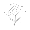
- FIG. 2 is a perspective view of the imaging device 50 according to the present embodiment.
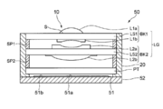
- FIG. 3 is a cross-sectional view of the configuration of FIG. 2 taken along the line III-III and the optical axis and viewed in the direction of the arrow. It is.
- the imaging device 50 includes a CMOS image sensor 51 as a solid-state imaging device having a photoelectric conversion unit 51 a, an imaging lens 10 that causes the photoelectric conversion unit 51 a of the image sensor 51 to capture a subject image, A substrate 52 having an external connection terminal (not shown) for holding the image sensor 51 and transmitting / receiving the electric signal is provided, and these are integrally formed.
- the imaging lens 10 is held by a housing 20 and has a first lens block BK1 and a second lens block BK2 in order from the object side.
- a photoelectric conversion unit 51a as a light receiving unit in which pixels (photoelectric conversion elements) are two-dimensionally arranged is formed in the center of a plane on the light receiving side.
- a processing circuit 51b is formed.
- the signal processing circuit 51b forms a picture signal output by using a drive circuit unit that sequentially drives each pixel to obtain a signal charge, an A / D conversion unit that converts each signal charge into a digital signal, and the digital signal. It consists of a signal processing unit and the like.
- a number of pads (not shown) are arranged near the outer edge of the plane on the light receiving side of the image sensor 51, and are connected to the substrate 52 via wires (not shown).
- the image sensor 51 converts the signal charge from the photoelectric conversion unit 51a into an image signal such as a digital YUV signal, and outputs the image signal to a predetermined circuit on the substrate 52 via a wire (not shown).
- Y is a luminance signal
- the solid-state imaging device is not limited to the CMOS image sensor, and other devices such as a CCD may be used.
- the substrate 52 that supports the image sensor 51 is communicably connected to the image sensor 51 through a wiring (not shown).
- the substrate 52 is connected to an external circuit (for example, a control circuit included in a host device of a portable terminal mounted with an imaging device) via an external connection terminal (not shown), and a voltage for driving the image sensor 51 from the external circuit. And a clock signal can be received, and a digital YUV signal can be output to an external circuit.
- an external circuit for example, a control circuit included in a host device of a portable terminal mounted with an imaging device
- an external connection terminal not shown
- a clock signal can be received, and a digital YUV signal can be output to an external circuit.
- the upper part of the image sensor 51 is sealed with a parallel plate PT such as an infrared cut filter fixed on the upper surface of the substrate 52.
- the lower end of the second spacer member SP2 is fixed to the upper surface around the parallel plate PT.
- the periphery of the second lens substrate LS2 of the second lens block BK2 is fixed to the upper end of the second spacer member SP2, and the lower end of the first spacer member SP1 is fixed to the upper surface of the periphery of the second lens substrate LS2.
- the periphery of the first lens substrate LS1 of the first lens block BK1 is fixed to the upper end of the spacer member SP1.
- the first lens block BK1 includes a first lens substrate LS1 that is a parallel plate made of glass, a first object-side lens portion (first a lens) L1a that is fixed to the object side surface, and a first lens substrate LS1.
- the first image side lens portion (first b lens) L1b made of resin fixed to the image side surface of the first image side lens.
- an aperture stop S is formed by an optical thin film formed on the surface of the first lens substrate LS1.
- the second lens block BK2 includes a second lens substrate LS2 that is a parallel plate made of glass, a second object-side lens portion (second a lens) L2a that is fixed to the object side surface, and a second lens substrate LS2. And a second image-side lens portion (second b lens) L2b made of resin fixed to the image side surface.
- the lens block LG is configured by the first lens block BK1 and the second lens block BK2
- the maximum light beam height of the axial light beam passing through the lens block LG becomes the maximum light beam height of the axial light beam of the imaging lens 10. ing.
- the lens portion L1a which is a 1a lens, is made of a thermosetting resin or an ultraviolet curable resin material in which inorganic fine particles having a maximum length of 30 nanometers or less satisfying the conditional expression (1) are dispersed.
- the lens portions L1b, L2a, L2b may be formed of the same resin.
- dn / dT (1) Temperature change coefficient of refractive index of the material constituting the 1a lens L1a
- the lens portion can be formed only on the object side surface or the image side surface of the lens substrates LS1 and LS2.
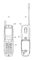
- FIG. 4 is a diagram illustrating a state in which the imaging device 50 is installed in a mobile phone 100 as a mobile terminal that is a digital device.
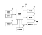
- FIG. 5 is a control block diagram of the mobile phone 100.
- the imaging device 50 is provided, for example, such that the object-side end surface of the imaging lens is provided on the back surface of the mobile phone 100 (the liquid crystal display unit side is the front surface) and is located at a position corresponding to the lower side of the liquid crystal display unit.
- the external connection terminal (not shown) of the imaging device 50 is connected to the control unit 101 of the mobile phone 100 and outputs an image signal such as a luminance signal or a color difference signal to the control unit 101 side.
- the mobile phone 100 controls each part in an integrated manner, and supports and inputs a control part (CPU) 101 that executes a program corresponding to each process, and a number and the like with keys.
- An input unit 60 a display unit 70 for displaying captured images and videos, a wireless communication unit 80 for realizing various information communications with an external server, a system program and various processing programs for the mobile phone 100,
- a storage unit (ROM) 91 that stores necessary data such as a terminal ID, and various processing programs and data executed by the control unit 101, processing data, imaging data by the imaging device 50, and the like are temporarily stored.
- a temporary storage unit (RAM) 92 used as a work area for storage.
- an image signal of a still image or a moving image is captured by the image sensor 51.
- the photographer presses the button BT shown in FIG. 4 at a desired photo opportunity the release is performed, and the image signal is taken into the imaging device 50.
- the image signal input from the imaging device 50 is transmitted to the control system of the mobile phone 100 and stored in the storage unit 92 or displayed on the display unit 70, and further, video information is transmitted via the wireless communication unit 80. Will be transmitted to the outside.
- FIG. 6 is a diagram illustrating a process of manufacturing the imaging lens according to the present embodiment.
- a lens block unit UT including a plurality of lens blocks BK arranged two-dimensionally is manufactured.
- Such a lens block unit UT can be manufactured by, for example, a replica method that can simultaneously manufacture a large number of lenses L and is low in cost.
- the number of lens blocks BK included in the lens block unit UT is at least two, but each lens block BK does not need to have lenses on both sides, and may be only on one side.
- the replica method is a method in which a plurality of curable resins PL are transferred in a lens shape at once using a mold onto a lens substrate LS which is a large parallel plate made of glass. That is, in the replica method, a large number of resin lenses PL are simultaneously manufactured on the lens substrate LS.
- the imaging lens 10 is manufactured from the lens block unit UT manufactured by these methods.
- An example of the manufacturing process of this imaging lens is shown in the schematic cross-sectional view of FIG.
- the first lens block unit UT1 includes a first lens substrate LS1 that is a parallel plate, a plurality of first object-side lens portions L1a that are bonded in a grid pattern on one plane, and a grid pattern that is bonded to the other plane. A plurality of first image side lens portions L1b. At this time, the first lens substrate LS1 and the first object side lens portion L1a are bonded using an adhesive via an optical thin film, and the first lens substrate LS1 and the first image side lens portion L1b are bonded to each other. Etc. are used for bonding.
- the entire lens length in the optical axis direction can be made smaller than that provided separately.
- an antireflection coating for example, a transparent thin film
- reflection at the lens portion and the lens substrate can be prevented, and flare and ghost can be reduced.
- the lens portions L1a and L1b and the lens substrate LS1 may be formed directly on the lens substrate LS1 without using an adhesive or the like.
- the second lens block unit UT2 includes a second lens that is a parallel plate, a plurality of second object-side lens portions L2a that are bonded in a grid pattern on one plane, and a grid pattern that is bonded to the other plane. And a plurality of second image side lens portions L2b.
- the second lens wafer LW2 and the second object side lens portion L2a are bonded using an adhesive
- the second lens and the second image side lens portion L2b are bonded using an adhesive or the like.
- the lens portions L2a and L2b and the lens may be formed directly on the lens substrate LS2 without using an adhesive or the like.
- a grid-shaped first spacer member (spacer) SP1 configured by a light-shielding member in which a plurality of light transmitting portions (openings through which light passes) is arranged in a grid pattern is used as the first lens block unit UT1 and the second lens. It is interposed between the block unit UT2 (specifically, between the second lens substrate LS2) and the distance between the lens block units UT1 and UT2 is kept constant. In this state, the lens portions L1a, L1b, L2a, and L2b align with the lattice holes of the first spacer member SP1 with the optical axes accurately aligned.
- a position reference mark for example, a fine pattern on the transfer surface of the mold
- a concave part is formed, a convex part formed by transferring at the time of molding, etc. is added, and by observing them optically, the position of the feature point in the observation coordinate system is calculated, and the position is adjusted so that they match
- the optical axes of the first lens block BK1 and the second lens block BK2 can be aligned with high precision (see Japanese Patent Application Laid-Open No. 2006-146043).
- the first spacer member SP1 is interposed between the first lens block unit UT1 and the second lens block unit UT2, the first lens substrate LS1 and the second lens substrate LS2 are sealed. Integrate.
- the lens block LG that is a component of the imaging lens 10 is manufactured by separating the members in which the plurality of lens blocks BK (the first lens block BK1 and the second lens block BK2) are incorporated, Adjustment and assembly of each lens interval of the imaging lens 10 are simplified. Therefore, mass production of imaging devices that are expected to have high image quality is possible.
- the first spacer member SP1 since the first spacer member SP1 has a lattice shape, the first spacer member SP1 also serves as a mark when the lens blocks LG are separated from the member in which the plurality of lens blocks BK1 and BK2 are incorporated. Therefore, the lens block LG can be easily cut out from the members incorporated in the plurality of lens blocks BK, and it does not take time and effort. As a result, the lens block LG can be mass-produced at a low cost.
- the first spacer member SP1 is arranged on at least a part of the periphery of the lens blocks BK1 and BK2, and the lens substrates of the plurality of lens block units UT1 and UT2 are arranged.
- Such a manufacturing method is suitable for mass production of an inexpensive lens system. It is sufficient to connect the two lens blocks via the spacer member, but three or more lens blocks may be connected.
- f Focal length of the entire imaging lens system fB: Back focus
- F F number 2Y: Diagonal length of the imaging surface of the solid-state imaging device
- ENTP Entrance pupil position (distance from the first surface to the entrance pupil position)
- EXTP exit pupil position (distance from imaging surface to exit pupil position)
- H1 Front principal point position (distance from first surface to front principal point position)
- H2 Rear principal point position (distance from the final surface to the rear principal point position)
- R radius of curvature
- D axial distance between axes
- Nd refractive index of lens material with respect to d-line
- ⁇ d Abbe number of lens material
- the aspherical shape has the vertex of the surface as the origin and the optical axis direction as the X axis In the orthogonal coordinate system, the vertex curvature is C, the conic constant is K, and the aspherical coefficients are A4, A6, A8, A10, A12, A14
- Tables 1 and 2 show lens data according to this example.
- a power of 10 for example, 2.5 ⁇ 10 ⁇ 3
- E for example, 2.5 ⁇ E ⁇ 3
- Example 1 shows lens data in Example 1.
- Example 1 is based on a design value (20 ° C.).
- the imaging device targeted in Example 1 is assumed to be a 1/5 inch type, a pixel pitch of 1.75 ⁇ m, and 1600 ⁇ 1200 pixels.
- 7 is a sectional view of the lens of Example 1.
- a first lens block BK1 is composed of a first a lens L1a convex to the object side, an aperture stop S, a first lens substrate LS1, and a first b lens L1b concave to the image side.
- the second lens block BK2 is composed of a concave second a lens L2a, a second lens substrate LS2, and a concave second b lens L2b on the image side.
- an optical low-pass filter an infrared cut filter, and a solid-state image sensor
- a parallel plate PT assuming a seal glass or the like is provided.
- IM is an imaging surface of the image sensor. Further, the surfaces of the lens portions that are in contact with all air are aspherical.
- the first lens block BK1 has a positive refractive power
- the second lens block BK2 has a negative refractive power.
- the 1a lens, 1b lens, 2a lens, and 2b lens of Example 1 are made of a curable resin material.
- FIG. 8 is an aberration diagram of spherical aberration (a), astigmatism (b), and distortion (c) of the imaging lens according to the first example.
- d represents the amount of spherical aberration with respect to the d line
- g represents the amount of spherical aberration with respect to the g line.
- the solid line represents the sagittal plane
- the dotted line represents the meridional plane.
- ⁇ 8.1 ⁇ 10 ⁇ 5
- f / f1 1.79 in the conditional expression (4)
- ⁇ 1 ⁇ 2 22 in the conditional expression (5).
- Table 2 shows the curvature radius, the axial top surface spacing, and the aspheric coefficient data of the imaging lens shown in Example 1 in a state where the environmental temperature is increased by 20 degrees (40 ° C.).
- the surface shape and thickness were obtained by thermal stress analysis using a finite element method. Specifically, the stress and displacement generated in the object due to the temperature difference are obtained, and the surface shape and thickness are calculated from the result of the lens shape at the assumed temperature (same in Table 8).
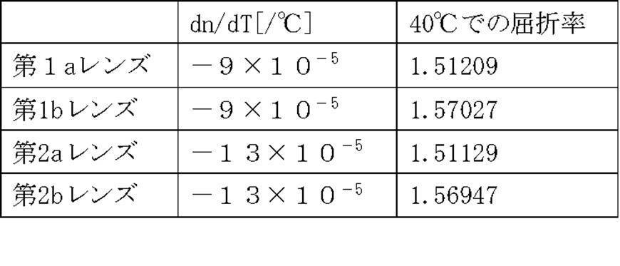
- Table 3 shows changes in the refractive index nd with temperature in Example 1.
- the back focus change amount ( ⁇ fB) at the time of + 20 ° C. increase with respect to the design value (20 ° C.) is ⁇ 0.004 [mm].
- Table 5 shows another example of the refractive index nd at the time of temperature change when the lens material is changed in Example 1. Accordingly, the back focus change amount ( ⁇ fB) at the time of + 20 ° C. increase with respect to the design value (20 ° C.) is +0.009 [mm].
- Table 6 shows another example of the refractive index nd at the time of temperature change when the lens material is changed in Example 1. Accordingly, the back focus change amount ( ⁇ fB) at the time of + 20 ° C. increase with respect to the design value (20 ° C.) is +0.010 [mm].
- the depth of focus is expressed by the following formula.
- Depth of focus ⁇ F number ⁇ 2 ⁇ pixel pitch
- the image point position variation must be less than the depth of focus at the maximum. Since the imaging lens assumed in Example 1 has an F number of 2.9 and the imaging device has a pixel pitch of 1.75 ⁇ m, the depth of focus is ⁇ 0.010, and the image point position variation is suppressed within the depth of focus. . Although the temperature change to the minus side is omitted, the image point position fluctuates by substantially the same amount as an absolute value on the opposite side to the sign side opposite to the plus side. (Example 2) Table 7 shows lens data in Example 2. Example 2 is based on the design value (20 ° C.).
- FIG. 9 is a sectional view of the lens of Example 2.
- a first lens block BK1 is composed of a first a lens L1a convex to the object side, an aperture stop S, a first lens substrate LS1, and a first b lens L1b concave to the image side.
- the second lens block BK2 is composed of a concave second a lens L2a, a second lens substrate LS2, and a concave second b lens L2b on the image side.
- an optical low-pass filter an infrared cut filter, and a solid-state image sensor
- a parallel plate PT assuming a seal glass or the like is provided.
- IM is an imaging surface of the image sensor. Further, the surfaces of the lens portions that are in contact with all air are aspherical.
- the first lens block BK1 has a positive refractive power
- the second lens block BK2 has a negative refractive power.
- the 1a lens, 1b lens, 2a lens, and 2b lens of Example 2 are made of a curable resin material.
- FIG. 10 is an aberration diagram of spherical aberration (a), astigmatism (b), and distortion (c) of the imaging lens according to the second example.
- d represents the amount of spherical aberration with respect to the d line
- g represents the amount of spherical aberration with respect to the g line.
- the solid line represents the sagittal plane
- the dotted line represents the meridional plane.
- ⁇ 8.1 ⁇ 10 ⁇ 5
- the conditional expression f / f1 1.71 in the conditional expression (4)
- ⁇ 1 ⁇ 2 22 in the conditional expression (5).
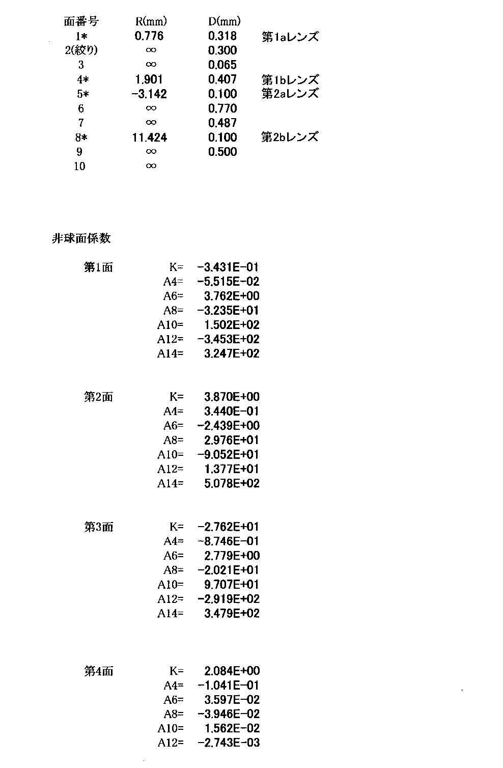
- Table 8 shows the curvature radius, the axial top surface spacing, and the aspheric coefficient data of the imaging lens shown in Example 2 in a state where the environmental temperature is increased by 20 degrees (40 ° C.).
- Table 9 shows changes in the refractive index nd with temperature in Example 2.
- the back focus change amount ( ⁇ fB) at the time of + 20 ° C. increase with respect to the design value (20 ° C.) is ⁇ 0.004 [mm].
- Table 10 shows another example of the refractive index nd at the time of temperature change when the lens material is changed in Example 2.
- the back focus change amount ( ⁇ fB) at the time of + 20 ° C. increase with respect to the design value (20 ° C.) is ⁇ 0.002 [mm].
- Table 11 shows another example of the refractive index nd at the time of temperature change when the lens material is changed in Example 2. Accordingly, the back focus change amount ( ⁇ fB) at the time of + 20 ° C. increase with respect to the design value (20 ° C.) is +0.010 [mm].
- the depth of focus is expressed by the following formula.
- Depth of focus ⁇ F number ⁇ 2 ⁇ pixel pitch
- the image point position variation must be less than the depth of focus at the maximum. Since the imaging lens assumed in Example 2 has an F number of 2.9 and the imaging element has a pixel pitch of 1.75 ⁇ m, the depth of focus is ⁇ 0.010, and the image point position variation is suppressed within the depth of focus. Yes. Although the temperature change to the minus side is omitted, the image point position fluctuates by substantially the same amount as an absolute value on the opposite side to the sign side opposite to the plus side.
- a mobile terminal is not limited to a mobile phone.
- Imaging lens 20 Case 50 Imaging device 51 Image sensor 51a Photoelectric conversion part 51b Signal processing circuit 52 Board
Landscapes
- Physics & Mathematics (AREA)
- General Physics & Mathematics (AREA)
- Optics & Photonics (AREA)
- Lenses (AREA)
Abstract
大量生産性と小型化に最適で、温度上昇に伴う樹脂レンズの屈折率変化及びレンズ面の形状変化に起因するピントずれを抑えることができる撮像レンズを提供する。 この撮像レンズは、平行平板であるレンズ基板の物体側面及び像側面の少なくとも一方に形成され、正又は負のパワーを有するレンズ部をそれぞれ備えてなり、レンズ部とレンズ基板は屈折率とアッベ数のうち少なくとも一方が異なっており、レンズ基板の両側にレンズ部が形成されたレンズブロックを少なくとも1個含む撮像レンズにおいて、最も物体側に配置されるレンズブロックを第1レンズブロックとし、第1レンズブロックの物体側に形成されたレンズ部を第1aレンズとするとき、第1aレンズが正の屈折力を有し、以下の式を満たすことを特徴とする。 -9×10⁻⁵/℃≦dn/dT(1)≦-2×10-5/℃ ただし、 dn/dT(1):第1aレンズを構成する材料の屈折率の温度変化係数
Description
本発明は、CCD(Charge Coupled Devices)型イメージセンサやCMOS(Complementary Metal-Oxide Semiconductor)型イメージセンサ等の固体撮像素子を用いた撮像装置の撮像レンズに関するものであり、より詳しくは、大量生産に適するレンズを用いた撮像レンズ及び撮像レンズを用いた撮像装置並びに携帯端末に関するものである。
近年、小型で薄型の撮像装置が、携帯電話機やPDA(Personal Digital Assistant)等の小型で薄型の電子機器である携帯端末に搭載されるようになり、これにより音声情報だけでなく画像情報も遠隔地と相互に伝送することが可能となっている。その撮像装置に使用される撮像素子としては、CCD(Charge Coupled Device)型イメージセンサやCMOS(Complementary Metal-Oxide Semiconductor)型イメージセンサ等の固体撮像素子が使用されている。また、撮像素子上に被写体像を形成するための撮像レンズとしては、安価に大量生産でき、非球面の付加が容易な樹脂レンズが低コスト化および小型化のために用いられている。
また、近年の携帯端末では、撮像レンズが搭載された撮像装置をプリント配線基板に実装する手法として、リフロー半田付け(Reflow soldering)処理が採用されている。以降、この処理をリフロー工程と称する。リフロー工程においては、プリント配線基板上に電子部品を配置する箇所にあらかじめ半田を配置し、そこへ電子部品を配置してから加熱して半田を溶融させた後、冷却することで、電子部品をプリント配線基板へ実装する。電子部品は、リフロー工程用の炉の内部で自動実装される。このようなリフロー工程の採用により、部品類のプリント配線基板への実装コストが安価となり、また、製造品質を一定に保つことができる。このようなリフロー工程による撮像装置の実装を可能とするため、リフロー工程に耐え得る耐熱性に優れた撮像レンズも求められている。
このような大量生産性と小型化、高耐熱性を有する撮像レンズの製造方法のひとつに、平行平板である数インチのガラス基板上に、高耐熱の硬化性樹脂で構成された多数のレンズを同時に形成するレプリカ法(replica method)がある。レプリカ法を用いてレンズ要素を同時に大量に成形し、これらのレンズ要素が多数形成されたガラス基板(レンズウェハ)をセンサーウェハと組み合わせた後切り離し、カメラモジュールを大量生産する方法が提案されているが、このような製法によって製造されたレンズをウェハスケールレンズ(Wafer scale lens)、またカメラモジュールをウェハスケールカメラモジュール(Wafer scale camera module)と呼ばれることもある。
しかし、一般に、樹脂レンズにおいては、ガラスレンズに比べ温度変化に対する屈折率変化が大きく、動作温度によって像点位置の変動、すなわちピントずれが起きてしまい、性能が劣化してしまう恐れがある。また、一般に、樹脂レンズの線膨張係数はガラスのそれに比べて大きいため、温度上昇に伴う熱膨張によって、レンズ部の近軸曲率半径が変化し、このことからも、ピントずれが起きてしまい、性能が劣化してしまう恐れがある。
これに対し、例えば特許文献1では、プラスチック材料中に30ナノメートル以下の無機微粒子を分散させ、プラスチック材料の温度変化を小さくし、温度変化による像点位置変動を抑制する手法が開示されている。
しかし、例えば特許文献1に記載の撮像レンズであっても、薄形の携帯端末等に搭載するためには、より小型化したいという要求があり、また温度変化による撮像レンズ全系の像点位置変動を更に抑制したいという要求もある。しかしながら、特許文献1には、撮像レンズの更なる小型化と、温度変化による撮像レンズ全系の像点位置変動とを実現する具体的な構成が開示されていない。
本発明は、上記の問題点を解決するためになされたものであって、その目的は、大量生産性と小型化に最適な、さらには、温度上昇に伴う樹脂レンズの屈折率変化およびレンズ面の形状変化に起因するピントずれを抑えることができる撮像レンズと、その撮像レンズを有する撮像装置と、その撮像装置を有する携帯端末とを提供することにある。
請求項1に記載の撮像レンズは、平行平板であるレンズ基板と、前記レンズ基板の物体側面及び像側面の少なくとも一方に形成され、正または負のパワーを有するレンズ部とをそれぞれ備えてなり、前記レンズ部と前記レンズ基板とは屈折率とアッベ数のうち少なくとも一方が異なっており、このようなレンズ群をレンズブロックとして、前記レンズ基板の両側にレンズ部が形成された前記レンズブロックを少なくとも1個含む撮像レンズにおいて、最も物体側に配置されるレンズブロックを第1レンズブロックとし、第1レンズブロックの物体側に形成されたレンズ部を第1aレンズとするとき、
前記第1aレンズが正の屈折力を有し、以下の式を満たすことを特徴とする撮像レンズ。
前記第1aレンズが正の屈折力を有し、以下の式を満たすことを特徴とする撮像レンズ。
-9×10⁻⁵/℃≦dn/dT(1)≦-2×10-5/℃ (1)
ただし、
dn/dT(1):第1aレンズを構成する材料の、屈折率の温度変化係数
撮像レンズ全系の小型化を実現するためには、撮像レンズ全系の主点位置を物体側へ寄せる必要があり、結果として第1aレンズの正の屈折力を強くしなくてはならない。しかしながら、第1aレンズの温度依存性が大きいと、強い正の屈折力と相まって、像点位置変動が大きくなる。そこで、第1aレンズに屈折率の温度依存性の小さい材料を用いることにより、温度変化時の像点位置変動を小さく抑えることができる。具体的には、第1aレンズの材料の屈折率の温度変化係数を、一般的な樹脂(アクリル系、ポリカーボネイト系、ポリオレフィン系など)の樹脂の屈折率の温度変化係数の
-10~12×10-5/℃より、絶対値として小さくするのが望ましいため、条件式(1)の下限を規定したのである。一方、第1aレンズの材料の屈折率の温度変化係数が条件式(1)の上限を超えてゼロに近づくと、負屈折力のレンズの屈折率変化による像点位置変動との相殺ができず好ましくない。そこで、第1aレンズを構成する材料の屈折率の温度変化係数は条件式(1)を満たすのが良いのである。
ただし、
dn/dT(1):第1aレンズを構成する材料の、屈折率の温度変化係数
撮像レンズ全系の小型化を実現するためには、撮像レンズ全系の主点位置を物体側へ寄せる必要があり、結果として第1aレンズの正の屈折力を強くしなくてはならない。しかしながら、第1aレンズの温度依存性が大きいと、強い正の屈折力と相まって、像点位置変動が大きくなる。そこで、第1aレンズに屈折率の温度依存性の小さい材料を用いることにより、温度変化時の像点位置変動を小さく抑えることができる。具体的には、第1aレンズの材料の屈折率の温度変化係数を、一般的な樹脂(アクリル系、ポリカーボネイト系、ポリオレフィン系など)の樹脂の屈折率の温度変化係数の
-10~12×10-5/℃より、絶対値として小さくするのが望ましいため、条件式(1)の下限を規定したのである。一方、第1aレンズの材料の屈折率の温度変化係数が条件式(1)の上限を超えてゼロに近づくと、負屈折力のレンズの屈折率変化による像点位置変動との相殺ができず好ましくない。そこで、第1aレンズを構成する材料の屈折率の温度変化係数は条件式(1)を満たすのが良いのである。
請求項2に記載の撮像レンズは、請求項1に記載の発明において、前記撮像レンズは、前記レンズ基板の物体側面及び像側面上の少なくとも一方に形成される負の屈折力を有するレンズ部を有し、以下の式を満たすことを特徴とする。
-14×10-5/℃≦dn/dT(N)≦-9×10-5/℃ (2)
ただし、
dn/dT(N):前記負の屈折力を有するレンズ部を構成する材料の、屈折率の温度変化係数
正屈折力のレンズの場合、温度が上昇したとき、樹脂材料の屈折率が低下して、焦点距離が長くなり像点位置が変化する。従って、正屈折力のレンズに屈折率の温度変化係数の相対的に小さい材料を用い、負屈折力のレンズに屈折率の温度変化係数の相対的に大きい材料を用いることでこれを抑制することができる。即ち条件式(2)は、正屈折力のレンズの温度変化時の像点移動を、負屈折力のレンズで相殺するための条件を規定する。
ただし、
dn/dT(N):前記負の屈折力を有するレンズ部を構成する材料の、屈折率の温度変化係数
正屈折力のレンズの場合、温度が上昇したとき、樹脂材料の屈折率が低下して、焦点距離が長くなり像点位置が変化する。従って、正屈折力のレンズに屈折率の温度変化係数の相対的に小さい材料を用い、負屈折力のレンズに屈折率の温度変化係数の相対的に大きい材料を用いることでこれを抑制することができる。即ち条件式(2)は、正屈折力のレンズの温度変化時の像点移動を、負屈折力のレンズで相殺するための条件を規定する。
請求項3に記載の撮像レンズは、請求項1又は2に記載の発明において、前記第1レンズブロックの像側に、所定間隔を隔て、少なくとも1つのレンズブロックが配置されることを特徴とする。
第1レンズブロックの像側に、所定間隔を隔て、少なくとも1つのレンズブロックが配置されることにより、光学的な屈折面を多く配置することができ、諸収差を良好に補正することができる。
請求項4に記載の撮像レンズは、請求項1~3のいずれかに記載の発明において、前記レンズ基板はガラス材料から形成され、前記第1aレンズの材料の線膨張係数αが次式を満たすこと特徴とする。
4×10⁻⁵≦α≦10×10-5 (3)
一般の樹脂レンズは、温度上昇が起こるとそれに伴って自由熱膨張し、近軸曲率半径が大きくなるような面形状変化を起こす。この場合、正屈折力のレンズでは、温度上昇に伴ってレンズの焦点距離が伸び、レンズ全系の近軸像点位置が設計値よりもバックフォーカスが長くなる方向へ移動する。しかし、レンズ基板がガラス材料から形成され、例えばレンズ部が樹脂材料から形成されたウェハスケールレンズの場合は、線膨張係数(樹脂材料の線膨張係数はガラスの線膨張係数より大きい)の差により、レンズ部は特有の面形状変化を起こす。つまり、レンズ部では、温度上昇に伴う光軸に垂直な方向(有効径方向)の熱膨張が抑制され、光軸方向の熱膨張が顕著となることから、正屈折力のレンズの場合は、近軸曲率半径が小さくなるように面形状が変化する。このようなレンズ部の温度上昇に伴う面形状変化は、上述した一般のレンズとは逆の変化であり、レンズ全系の近軸像点位置を設計値よりもバックフォーカスが短くなる方向へ移動する。これを、シミュレーションに基づく図1を元に説明する。
一般の樹脂レンズは、温度上昇が起こるとそれに伴って自由熱膨張し、近軸曲率半径が大きくなるような面形状変化を起こす。この場合、正屈折力のレンズでは、温度上昇に伴ってレンズの焦点距離が伸び、レンズ全系の近軸像点位置が設計値よりもバックフォーカスが長くなる方向へ移動する。しかし、レンズ基板がガラス材料から形成され、例えばレンズ部が樹脂材料から形成されたウェハスケールレンズの場合は、線膨張係数(樹脂材料の線膨張係数はガラスの線膨張係数より大きい)の差により、レンズ部は特有の面形状変化を起こす。つまり、レンズ部では、温度上昇に伴う光軸に垂直な方向(有効径方向)の熱膨張が抑制され、光軸方向の熱膨張が顕著となることから、正屈折力のレンズの場合は、近軸曲率半径が小さくなるように面形状が変化する。このようなレンズ部の温度上昇に伴う面形状変化は、上述した一般のレンズとは逆の変化であり、レンズ全系の近軸像点位置を設計値よりもバックフォーカスが短くなる方向へ移動する。これを、シミュレーションに基づく図1を元に説明する。
ここで、図1(a)~(d)は、例えばガラス製のレンズ基板上に樹脂レンズを形成した4つの例を模式的に示す図であって、設計値(20℃)からプラス20度の温度変化後のレンズ面形状の変化を模式的に示している。各樹脂レンズは、光学的機能を発揮するレンズ部L1a~L2bと、レンズ部の周囲に形成されたコバ部C1~C4とを有するものとする。なお、図中、温度変化に伴って面形状が変化した後のその面形状(空気との界面)を破線で示す。また、第1aレンズL1a~第2bレンズL2bは、それぞれ光軸AXを中心とする回転対称な形状であるため、その半分のみを図示している。
第1aレンズL1a~第2bレンズL2bの面形状は、いずれも温度変化に伴って変化していることがわかる。しかるに、図1(b)に示す負のパワーを持つ第1bレンズL1bに関しては、光学面形状変化には大きな影響を与えていないと言える。
一方、図1(c)に示す負のパワーを持つ第2aレンズL2aでは、光学面形状変化への影響が第1bレンズL1bより大きい。しかし、第2aレンズL2aは、軸上光線の通過高さが第1aレンズL1aおよび第1bレンズL1bにくらべ低いので、ピントズレへ与える影響が小さい。なお、図1(d)に示す負のパワーを持つ第2bレンズL2bでは、近軸焦点距離が長いため、その面形状はなだらかであり、ピントズレにはあまり影響を与えない。
これに対し、図1(a)に示す正のパワーを持つ第1aレンズL1aでは、光学面形状変化に大きな影響を与えており、近軸曲率半径が小さくなるように面形状が変化していることがわかる。
したがって、ウェハスケールレンズでは、近軸曲率半径が温度変化に伴って小さくなるレンズ部の面形状変化によるレンズ全系の近軸像点位置の変化が、温度変化に伴うレンズ部の屈折率変化によるレンズ全系の近軸像点位置の変化と相反することとなる。実際、温度上昇に伴うレンズ部の近軸曲率半径の変化が近軸像点位置へ及ぼす影響が、温度変化に伴うレンズ部の屈折率変化が近軸像点位置へ及ぼす影響と相反することがシミュレーションによって確かめられた。なお、このシミュレーションは、可逆変化を想定した応力解析である。以上より、撮像レンズの小型化を図るべく、最も物体側のレンズ(第1aレンズ)を樹脂製としたウェハスケールレンズを用いると、温度変化によるピントズレが顕著になる傾向があるといえるため、第1aレンズに条件式(1)を満たす材料を用いると効果的である。
更に、条件式(3)の値が上限を超えて線膨張係数が大きくなると、温度上昇時の面形状変化が大きくなりすぎ、リフロー工程を通した場合に、レンズ表面のARコートにクラックが発生することが懸念されるため好ましくない。条件式(3)の値が下限を下回ると、温度変化時の屈折率変化による像点位置変動と、面形状変化による像点位置変動との相殺効果が小さくなりすぎ好ましくない。よって、条件式(3)を満たすのが好ましい。
請求項5に記載の撮像レンズは、請求項1~4のいずれかに記載の発明において、下式を満たすことを特徴とする。
1.0≦f/f1a≦3.0 (4)
ただし、
f:撮像レンズ全系の焦点距離(mm)
f1a:第1aレンズの空気中での焦点距離(mm)
条件式(4)は、第1aレンズの焦点距離を適切に設定し撮像レンズ全長の短縮化と収差補正を適切に達成するための条件を規定する。条件式(4)の値が上限を下回ることで、第1aレンズの屈折力を適度に維持することができ、撮像レンズ全系の合成主点をより物体側へ配置することができ、撮像レンズ全長を短くすることができる。一方、条件式(4)の値が下限を上回ることで、第1aレンズの屈折力が必要以上に大きくなりすぎず、第1aレンズで発生する、高次の球面収差やコマ収差を小さく抑えることができる。
ただし、
f:撮像レンズ全系の焦点距離(mm)
f1a:第1aレンズの空気中での焦点距離(mm)
条件式(4)は、第1aレンズの焦点距離を適切に設定し撮像レンズ全長の短縮化と収差補正を適切に達成するための条件を規定する。条件式(4)の値が上限を下回ることで、第1aレンズの屈折力を適度に維持することができ、撮像レンズ全系の合成主点をより物体側へ配置することができ、撮像レンズ全長を短くすることができる。一方、条件式(4)の値が下限を上回ることで、第1aレンズの屈折力が必要以上に大きくなりすぎず、第1aレンズで発生する、高次の球面収差やコマ収差を小さく抑えることができる。
なお本発明により温度上昇に伴うピントズレを抑制するためには、撮像レンズは以下の条件を満たすことが望ましい。
2.0(mm)≦f≦4.0(mm)
さらに望ましくは、
2.4(mm)≦f≦3.0(mm)
である。
さらに望ましくは、
2.4(mm)≦f≦3.0(mm)
である。
又、Fを撮像レンズのFナンバーとしたときに、撮像レンズは以下の条件を満たすことが望ましい。
2.0≦F≦4.0
さらに望ましくは、
2.5≦F≦3.5
である。
さらに望ましくは、
2.5≦F≦3.5
である。
更に、pを撮像レンズに使用される撮像素子のピクセルサイズしたときに、撮像レンズは以下の条件を満たすことが望ましい。
1.2μm≦p≦2.0μm
さらに望ましくは、
1.5μm≦p≦1.8μm
である。
さらに望ましくは、
1.5μm≦p≦1.8μm
である。
請求項6に記載の撮像レンズは、請求項1~5のいずれかに記載の発明において、前記第1レンズブロックの像側に形成されたレンズを第1bレンズとするとき、第1bレンズは負の屈折力を有し、以下の条件式を満たすことを特徴とする。
10<ν1a-ν1b<40 (5)
ただし、
ν1a:前記第1aレンズを構成する材料のアッベ数
ν1b:前記第1bレンズを構成する材料のアッベ数
第1レンズブロックは、正の屈折力を有する第1aレンズと負の屈折力を有する第1bレンズを備えることで、色収差を補正している。条件式(5)を満たす材料を用いることで色収差の補正が良好になるが、条件式(5)の値が下限を下回ると軸上色収差が補正不足となり好ましくない。一方、条件式(5)の値が上限を上回ると、負屈折力の第1bレンズで倍率色収差が過度に発生し、他の面で補正することが困難になるため好ましくない。従って、条件式(5)を満たすのが好ましい。
ただし、
ν1a:前記第1aレンズを構成する材料のアッベ数
ν1b:前記第1bレンズを構成する材料のアッベ数
第1レンズブロックは、正の屈折力を有する第1aレンズと負の屈折力を有する第1bレンズを備えることで、色収差を補正している。条件式(5)を満たす材料を用いることで色収差の補正が良好になるが、条件式(5)の値が下限を下回ると軸上色収差が補正不足となり好ましくない。一方、条件式(5)の値が上限を上回ると、負屈折力の第1bレンズで倍率色収差が過度に発生し、他の面で補正することが困難になるため好ましくない。従って、条件式(5)を満たすのが好ましい。
請求項7に記載の撮像レンズは、請求項1~6のいずれかに記載の発明において、前記第1aレンズは樹脂材料から構成されること特徴とする。
第1aレンズの材料に樹脂材料を用いることで、コストを下げ、容易に大量生産することができる。
請求項8に記載の撮像レンズは、請求項1~7のいずれかに記載の発明において、前記第1aレンズの樹脂材料には、長さ30ナノメートル以下の無機微粒子が分散されていることを特徴とする。
樹脂材料にて構成されるレンズ部に30ナノメートル以下の無機微粒子を分散させることで、温度が変化しても性能の劣化や、像点位置変動を低減でき、しかも光透過率を低下させることなく、環境変化に関わらず優れた光学特性を有する撮像レンズを提供できる。
一般に透明な樹脂材料に微粒子を混合させると、光の散乱が生じ透過率が低下するため、光学材料として使用することは困難であったが、微粒子の大きさを透過光束の波長より小さくすることにより、散乱が実質的に発生しないようにできる。
また、樹脂材料はガラス材料に比べて屈折率が低いことが欠点であったが、屈折率の高い無機粒子を母材となる樹脂材料に分散させると、屈折率を高くできることが分かってきた。具体的には、母材となるプラスチック材料に30ナノメートル以下、なお、望ましくは、母材となる樹脂材料に20ナノメートル以下、更に望ましくは15ナノメートル以下の無機粒子を分散させることにより、任意の屈折率を有する材料を提供できる。
更に、樹脂材料は温度が上昇することにより屈折率が低下してしまうが、温度が上昇すると屈折率が上昇する無機粒子を母材となる樹脂材料に分散させると、これらの性質を打ち消しあうように作用するので、温度変化に対する屈折率変化を小さくできることも知られている。また、逆に、温度が上昇すると屈折率が低下する無機粒子を母材となる樹脂材料に分散させると、温度変化に対する屈折率変化を大きくできることも知られている。具体的には、母材となるプラスチック材料に30ナノメートル以下、なお、望ましくは、母材となる樹脂材料に20ナノメートル以下、更に望ましくは15ナノメートル以下の無機粒子を分散させることにより、任意の温度依存性を有する材料を提供できる。
例えば、アクリル系樹脂に酸化アルミニウム(Al2O3)やニオブ酸リチウム(LiNbO3)の微粒子を分散させることにより、高い屈折率のプラスチック材料が得られるとともに、温度に対する屈折率変化を小さくすることができる。こうした技術をもちいれば、本発明に係る実施形態におけるレンズ保持構造において、レンズ保持平板(例えば、第1レンズ基板)とレンズ部(例えば、第1aレンズ、第1bレンズ)との線膨張係数の差によってレンズ部の近軸曲率半径が小さくなることによる近軸像点位置への影響と打ち消し合う程度の屈折率の温度依存性を有する樹脂材料を採用することによってピントズレを良好に補正できる。
次に、屈折率の温度変化Aについて詳細に説明する。屈折率の温度変化Aは、ローレンツ・ローレンツの式に基づいて、屈折率nを温度tで微分することにより、以下の式で表される。

但し、
α:線膨張係数
[R]:分子屈折。
α:線膨張係数
[R]:分子屈折。
樹脂材料の場合は、一般に式中第1項に比べ第2項の寄与が小さく、ほぼ無視できる。例えば、PMMA樹脂の場合、線膨張係数αは7×10⁻⁵であり、上記式に代入すると、dn/dt=-1.2×10-4[/℃]となり、実測値とおおむね一致する。
ここで、微粒子、望ましくは無機微粒子を樹脂材料中に分散させることにより、実質的に上記式の第2項の寄与を大きくし、第1項の線膨張による変化と打ち消しあうようにさせている。具体的には、従来は-1.2×10⁻⁴程度であった変化を、絶対値で8×10⁻⁵未満に抑えることが望ましい。
混合させる割合は、屈折率の温度に対する変化の割合をコントロールするために、適宜増減できるし、複数種類のナノサイズの無機粒子をブレンドして分散させることも可能である。このような樹脂は、特開2007-126636号に開示されている。
請求項9に記載の撮像レンズは、請求項1~8のいずれかに記載の発明において、前記第1aレンズの樹脂材料は、硬化型樹脂であることを特徴とする。
請求項10に記載の撮像レンズは、請求項1~9のいずれかに記載の発明において、前記第1aレンズの樹脂材料は、UV硬化型樹脂であることを特徴とする。
第1aレンズを硬化型の樹脂材料によって構成することにより、平行平板であるガラス基板に、金型によって同時に大量に第1aレンズを種々の手段によって硬化させることが可能となり、量産性を向上させることができるようになる。ここで、硬化型の樹脂材料とは熱によって硬化する樹脂材料や光によって硬化する樹脂材料等を指す。なお、硬化型の樹脂材料はUV硬化型の樹脂材料によって構成されることが望ましい。UV硬化型の樹脂材料で構成されることにより、硬化時間を短くでき、量産性を改善できる。また、近年では耐熱性に優れた樹脂及び硬化型の樹脂材料が開発されており、リフロー処理にも耐えることができる。
請求項11に記載の撮像装置は、請求項1~10の何れかに記載の撮像レンズと、この撮像レンズで結像された物体像を光電変換するイメージセンサとを備えることを特徴とする。これにより小型で高画質な画像を撮像できる撮像装置を提供できる。
請求項12に記載の携帯端末は、請求項11に記載の撮像装置を備えることを特徴とする。
本発明によれば、大量生産性と小型化に最適な、さらには、温度上昇に伴う樹脂レンズの屈折率変化およびレンズ面の形状変化に起因するピントずれを抑えることができる撮像レンズと、その撮像レンズを有する撮像装置と、その撮像装置を有する携帯端末とを提供することができる。
以下、本発明の実施の形態を図面に基づいて説明する。図2は、本実施の形態にかかる撮像装置50の斜視図であり、図3は、図2の構成を矢印III-III線及び光軸を通る面で切断して矢印方向に見た断面図である。図3に示すように、撮像装置50は、光電変換部51aを有する固体撮像素子としてのCMOS型イメージセンサ51と、このイメージセンサ51の光電変換部51aに被写体像を撮像させる撮像レンズ10と、イメージセンサ51を保持すると共にその電気信号の送受を行う外部接続用端子(不図示)を有する基板52とを備え、これらが一体的に形成されている。尚、撮像レンズ10は、筐体20により保持されてなり、物体側から順に第1レンズブロックBK1と、第2レンズブロックBK2とを有する。
上記イメージセンサ51は、その受光側の平面の中央部に、画素(光電変換素子)が2次元的に配置された、受光部としての光電変換部51aが形成されており、その周囲には信号処理回路51bが形成されている。かかる信号処理回路51bは、各画素を順次駆動し信号電荷を得る駆動回路部と、各信号電荷をデジタル信号に変換するA/D変換部と、このデジタル信号を用いて画像信号出力を形成する信号処理部等から構成されている。また、イメージセンサ51の受光側の平面の外縁近傍には、多数のパッド(図示略)が配置されており、不図示のワイヤを介して基板52に接続されている。イメージセンサ51は、光電変換部51aからの信号電荷をデジタルYUV信号等の画像信号等に変換し、ワイヤ(不図示)を介して基板52上の所定の回路に出力する。ここで、Yは輝度信号、U(=R-Y)は赤と輝度信号との色差信号、V(=B-Y)は青と輝度信号との色差信号である。なお、固体撮像素子は上記CMOS型のイメージセンサに限定されるものではなく、CCD等の他のものを使用しても良い。
イメージセンサ51を支持する基板52は、不図示の配線により、イメージセンサ51に対して通信可能に接続されている。
基板52は、不図示の外部接続用端子を介して外部回路(例えば、撮像装置を実装した携帯端末の上位装置が有する制御回路)と接続し、外部回路からイメージセンサ51を駆動するための電圧やクロック信号の供給を受けたり、また、デジタルYUV信号を外部回路へ出力したりすることを可能とする。
イメージセンサ51の上部は、基板52の上面に固定された赤外線カットフィルタなどの平行平板PTにより封止されている。平行平板PTの周囲上面には、第2スペーサ部材SP2の下端が固定されている。第2スペーサ部材SP2の上端には、第2レンズブロックBK2の第2レンズ基板LS2周辺が固定され、第2レンズ基板LS2周辺の上面には、第1スペーサ部材SP1の下端が固定され、第1スペーサ部材SP1の上端には、第1レンズブロックBK1の第1レンズ基板LS1周辺が固定されている。
第1レンズブロックBK1は、ガラス製の平行平板である第1レンズ基板LS1と、その物体側面に固着された樹脂製の第1物体側レンズ部(第1aレンズ)L1aと、第1レンズ基板LS1の像側面に固着された樹脂製の第1像側レンズ部(第1bレンズ)L1bとからなる。第1物体側レンズ部L1aと第1レンズ基板LS1との間には、第1レンズ基板LS1の表面に成膜された光学薄膜により開口絞りSが形成されている。第2レンズブロックBK2は、ガラス製の平行平板である第2レンズ基板LS2と、その物体側面に固着された樹脂製の第2物体側レンズ部(第2aレンズ)L2aと、第2レンズ基板LS2の像側面に固着された樹脂製の第2像側レンズ部(第2bレンズ)L2bとからなる。第1レンズブロックBK1と第2レンズブロックBK2とでレンズブロックLGを構成したときに、レンズブロックLGを通過する軸上光束の最大光線高が、撮像レンズ10の軸上光束の最大光線高となっている。第1aレンズであるレンズ部L1aは、条件式(1)を満たす最大長30ナノメートル以下の無機微粒子を分散させた熱硬化性樹脂又は紫外線硬化性樹脂材料からなるが、レンズ部L1b、L2a、L2bも同様の樹脂で形成して良い。
-9×10⁻⁵/℃≦dn/dT(1)≦-2×10-5/℃ (1)
ただし、
dn/dT(1):第1aレンズL1aを構成する材料の、屈折率の温度変化係数
尚、レンズ基板LS1、LS2の物体側面もしくは像側面にのみ、レンズ部を形成することもできる。
ただし、
dn/dT(1):第1aレンズL1aを構成する材料の、屈折率の温度変化係数
尚、レンズ基板LS1、LS2の物体側面もしくは像側面にのみ、レンズ部を形成することもできる。
上述した撮像装置50の使用態様について説明する。図4は、撮像装置50をデジタル機器である携帯端末としての携帯電話機100に装備した状態を示す図である。また、図5は携帯電話機100の制御ブロック図である。
撮像装置50は、例えば、撮像レンズの物体側端面が携帯電話機100の背面(液晶表示部側を正面とする)に設けられ、液晶表示部の下方に相当する位置になるよう配設される。
撮像装置50の外部接続用端子(不図示)は、携帯電話機100の制御部101と接続され、輝度信号や色差信号等の画像信号を制御部101側に出力する。
一方、携帯電話機100は、図5に示すように、各部を統括的に制御すると共に、各処理に応じたプログラムを実行する制御部(CPU)101と、番号等をキーにより支持入力するための入力部60と、撮像した画像や映像等を表示する表示部70と、外部サーバとの間の各種情報通信を実現するための無線通信部80と、携帯電話機100のシステムプログラムや各種処理プログラム及び端末ID等の必要な諸データを記憶している記憶部(ROM)91と、制御部101によって実行される各種処理プログラムやデータ、若しくは処理データ、或いは撮像装置50による撮像データ等を一時的に格納する作業領域として用いられる一時記憶部(RAM)92とを備えている。
携帯電話機100を把持する撮影者が、被写体に対して撮像装置50の撮像レンズ10を向けると、イメージセンサ51に静止画又は動画の画像信号が取り込まれる。所望のシャッタチャンスで、図4に示すボタンBTを撮影者が押すことでレリーズが行われ、画像信号が撮像装置50に取り込まれることとなる。撮像装置50から入力された画像信号は、上記携帯電話機100の制御系に送信され、記憶部92に記憶されたり、或いは表示部70で表示され、さらには、無線通信部80を介して映像情報として外部に送信されることとなる。
本実施の形態にかかる撮像レンズの製造方法について説明する。図6は、本実施の形態にかかる撮像レンズを製造する工程を示す図である。まず、図6(a)の断面図に示すような、複数のレンズブロックBKを二次元的に並べて含むレンズブロックユニットUTを製造する。かかるレンズブロックユニットUTは、例えば、多数のレンズLを同時に作製できるとともに低コストであるレプリカ法で製造することができる。尚、レンズブロックユニットUTに含まれるレンズブロックBKの数は少なくとも2つであるが、各レンズブロックBKは、両側にレンズを有する必要はなく、片側のみでも良い。
また、レプリカ法とは、大版のガラス製の平行平板であるレンズ基板LS上に、金型を用いて硬化性の樹脂PLを複数個一度にレンズ形状にして転写するものである。つまり、レプリカ法では、レンズ基板LS上に、多数の樹脂レンズPLが同時に作製されることとなる。
そして、これらのような方法によって製造されたレンズブロックユニットUTから、撮像レンズ10が製造される。この撮像レンズの製造工程の一例を、図6(b)の概略断面図で示す。
第1のレンズブロックユニットUT1は、平行平板である第1レンズ基板LS1と、その一方の平面に格子状に接着された複数の第1物体側レンズ部L1aと、他方の平面に格子状に接着された複数の第1像側レンズ部L1bと、で構成される。このとき、第1レンズ基板LS1と第1物体側レンズ部L1aとは、光学薄膜を介して接着剤を用いて接着され、第1レンズ基板LS1と第1像側レンズ部L1bとは、接着剤等を用いて接着される。尚、光学薄膜や接着剤等を、赤外線カットフィルタや絞りの上に設けた場合には、別に設けるよりも光軸方向のレンズ全長を小さくできるので好ましい。更に、(透明薄膜、例えば)反射防止コートを設ければ、レンズ部とレンズ基板での反射を防止でき、フレアやゴーストを低減できる。尚、レンズ部L1aおよびL1bとレンズ基板LS1とは接着剤等を用いず、レンズ基板LS1上にレンズ部L1aおよびL1bを直接形成しても良い。
第2のレンズブロックユニットUT2は、平行平板である第2レンズと、その一方の平面に格子状に接着された複数の第2物体側レンズ部L2aと、他方の平面に格子状に接着された複数の第2像側レンズ部L2bと、で構成される。このとき、第2レンズウエハLW2と第2物体側レンズ部L2aとは、接着剤を用いて接着され、第2レンズと第2像側レンズ部L2bとは、接着剤等を用いて接着される。尚、レンズ部L2aおよびL2bとレンズとは接着剤等を用いず、レンズ基板LS2上にレンズ部L2aおよびL2bを直接形成しても良い。
複数の光透過部(光が通過する開口)が格子状に配置された遮光部材により構成される格子状の第1スペーサ部材(スペーサ)SP1を、第1のレンズブロックユニットUT1と第2のレンズブロックユニットUT2との間(具体的には、と第2レンズ基板LS2との間)に介在させ、両レンズブロックユニットUT1、UT2の間隔を一定に保つ。かかる状態で、第1スペーサ部材SP1の格子の穴の部分に、各レンズ部L1a、L1b、L2a、L2bが光軸を精度良く一致させて整列する。尚、光軸合わせを行う手段として、たとえば第1レンズ基板LS1と第2レンズ基板LS2上に他の部分と明るさの異なる特徴点として観察される位置基準マーク(例えば金型の転写面に微細な凹部を形成し、成形時に転写してなる凸部等)を付与し、それらを光学的に観察することで観察座標系内における特徴点の位置を算出し、それらが合致するように位置調整を行うことで、第1レンズブロックBK1と第2レンズブロックBK2の光軸を精度良く合わせることができる(特開2006-146043号公報参照)。
ここで、第1スペーサ部材SP1が、第1のレンズブロックユニットUT1と第2のレンズブロックユニットUT2との間に介在することで、第1レンズ基板LS1と第2レンズ基板LS2とが封止され一体化する。
そして、第1スペーサ部材SP1を介して連結された第1レンズ基板LS1と第2レンズ基板LS2が、第1スペーサ部材SP1の格子枠(破線Qの位置)に沿って切断されると、図6(c)に示すように、レンズブロック毎にそれぞれ一体化した2枚玉構成のレンズブロックLGが、複数個効率的に形成されることとなる。その後、形成された撮像レンズ10と平行平板PTとを、基板52に組み付けたイメージセンサ51に対向するようにして、筐体20で保持することにより、図3に示す撮像装置を得ることができる。
このように、複数のレンズブロックBK(第1レンズブロックBK1および第2レンズブロックBK2)の組み込まれた部材が切り離されることで、撮像レンズ10の構成要素であるレンズブロックLGが製造されると、撮像レンズ10の各レンズ間隔の調整および組み立てが簡素化される。そのため、高画質が期待される撮像装置の大量生産が可能となる。
しかも、第1スペーサ部材SP1が格子形状であるため、この第1スペーサ部材SP1が、複数のレンズブロックBK1,BK2の組み込まれた部材から、各レンズブロックLGを切り離す場合の印にもなる。したがって、複数のレンズブロックBKに組み込まれた部材からレンズブロックLGを容易に切り出すことができ、手間がかからない。その結果、レンズブロックLGを安価に大量生産できる。
以上を踏まえると、撮像レンズ10を構成するレンズブロックLGの製造方法は、レンズブロックBK1,BK2の周縁の少なくとも一部に第1スペーサ部材SP1を並べ、複数のレンズブロックユニットUT1,UT2のレンズ基板LS1、LS2同士を、格子状の第1スペーサ部材SP1を介在させて接着する連結工程と、これにより一体化されたレンズブロックユニットUT1,UT2を、第1スペーサ部材SP1に沿って切断する切断工程と、を含むものといえる。そして、このような製造方法は、安価なレンズ系の量産に向いている。尚、2つのレンズブロックを、スペーサ部材を介してつなげれば足りるが、3つ以上のレンズブロックをつなげても良い。
ここで、本実施の形態に好適な実施例について説明する。かかる実施例において使用する記号は下記の通りである。
f :撮像レンズ全系の焦点距離
fB :バックフォーカス
F :Fナンバー
2Y :固体撮像素子の撮像面対角線長
ENTP:入射瞳位置(第1面から入射瞳位置までの距離)
EXTP:射出瞳位置(撮像面から射出瞳位置までの距離)
H1 :前側主点位置(第1面から前側主点位置までの距離)
H2 :後側主点位置(最終面から後側主点位置までの距離)
R :曲率半径
D :軸上面間隔
Nd :レンズ材料のd線に対する屈折率
νd :レンズ材料のアッベ数
本実施例において、非球面の形状は、面の頂点を原点とし光軸方向をX軸とした直交座標系において、頂点曲率をC、円錐定数をK、非球面係数をA4、A6、A8、A10、A12、A14、A16をとして「数2」で表している。
fB :バックフォーカス
F :Fナンバー
2Y :固体撮像素子の撮像面対角線長
ENTP:入射瞳位置(第1面から入射瞳位置までの距離)
EXTP:射出瞳位置(撮像面から射出瞳位置までの距離)
H1 :前側主点位置(第1面から前側主点位置までの距離)
H2 :後側主点位置(最終面から後側主点位置までの距離)
R :曲率半径
D :軸上面間隔
Nd :レンズ材料のd線に対する屈折率
νd :レンズ材料のアッベ数
本実施例において、非球面の形状は、面の頂点を原点とし光軸方向をX軸とした直交座標系において、頂点曲率をC、円錐定数をK、非球面係数をA4、A6、A8、A10、A12、A14、A16をとして「数2」で表している。

ただし、h=√(Y2+Z2)である。
本実施例にかかるレンズデータを表1,2に示す。尚、表中では、10のべき乗数(例えば、2.5×10⁻³)を、E(例えば、2.5×E-3)を用いて表すものとする。
(実施例1)
実施例1におけるレンズデータを表1に示す。実施例1は、設計値(20℃)を基準としている。
(実施例1)
実施例1におけるレンズデータを表1に示す。実施例1は、設計値(20℃)を基準としている。
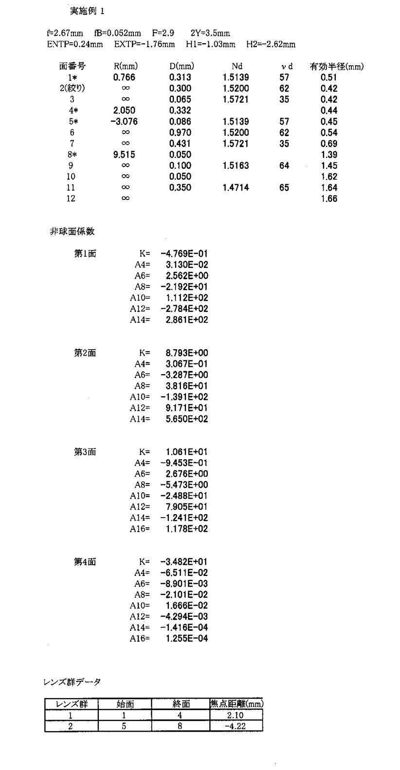
実施例1で対象とする撮像素子は、1/5インチ型、画素ピッチ1.75μm、1600×1200画素を想定している。図7は実施例1のレンズの断面図である。物体側から順に、物体側に凸の第1aレンズL1a、開口絞りS、第1レンズ基板LS1、像側に凹の第1bレンズL1bより、第1レンズブロックBK1が構成され、次に、物体側に凹の第2aレンズL2a、第2レンズ基板LS2、像側に凹の第2bレンズL2bより、第2レンズブロックBK2が構成され、最後に光学的ローパスフィルタ、赤外カットフィルタ、固体撮像素子のシールガラス等を想定した平行平板PTが設けられている。IMは撮像素子の撮像面である。また、全ての空気と接するレンズ部の面は非球面形状である。第1レンズブロックBK1は正の屈折力を有し、第2レンズブロックBK2は負の屈折力を有する。実施例1の第1aレンズ、第1bレンズ、第2aレンズ、第2bレンズは、硬化型樹脂材料で構成される。
図8は、実施例1にかかる撮像レンズの球面収差(a)、非点収差(b)、及び歪曲収差(c)の収差図である。ここで、球面収差図において、dはd線、gはg線に対する球面収差量をそれぞれ表す。また、非点収差図において、実線はサジタル面、点線はメリディオナル面をそれぞれ表す。条件式(3)におけるα=8.1×10⁻⁵であり、条件式(4)におけるf/f1=1.79であり、条件式(5)におけるν1-ν2=22である。
(+20℃温度変化時)
ここで、環境温度がプラス20度上昇した状態(40℃)での、実施例1に示す撮像レンズの曲率半径、軸上面間隔、非球面係数データを表2に示す。
(+20℃温度変化時)
ここで、環境温度がプラス20度上昇した状態(40℃)での、実施例1に示す撮像レンズの曲率半径、軸上面間隔、非球面係数データを表2に示す。

表2中、面形状、厚みは、有限要素法を用いた熱応力解析によって求めた。具体的には、温度差によって物体に生じる応力や変位を求め、想定される温度でのレンズ形状の結果から、面形状、厚みを算出している(表8において同じ)。
更に、実施例1において温度による屈折率ndの変化を表3に示す。これより、設計値(20℃)に対し+20℃上昇時のバックフォーカス変化量(ΔfB)は、-0.004[mm]となる。
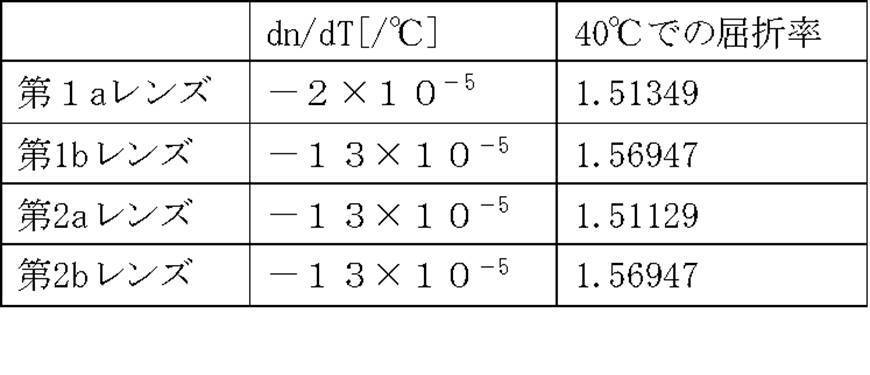
更に、実施例1においてレンズ材料を変更した場合における温度変化時の屈折率ndの別の例を表4に示す。これより、設計値(20℃)に対し+20℃上昇時のバックフォーカス変化量(ΔfB)は、-0.002[mm]となる。

更に、実施例1においてレンズ材料を変更した場合における温度変化時の屈折率ndの別の例を表5に示す。これより、設計値(20℃)に対し+20℃上昇時のバックフォーカス変化量(ΔfB)は、+0.009[mm]となる。
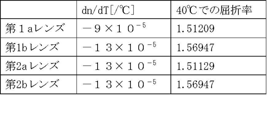
更に、実施例1においてレンズ材料を変更した場合における温度変化時の屈折率ndの別の例を表6に示す。これより、設計値(20℃)に対し+20℃上昇時のバックフォーカス変化量(ΔfB)は、+0.010[mm]となる。
一般的に焦点深度は下式で表される。
焦点深度=±Fナンバー×2×画素ピッチ
像点位置変動は、最大でも焦点深度以下にしなければならない。実施例1において想定した撮像レンズはFナンバー2.9、撮像素子は画素ピッチ1.75μmであるので、焦点深度は±0.010であり、像点位置変動は焦点深度内に抑えられている。また、マイナス側への温度変化は割愛するが、像点位置はプラス側と反対符号側へ絶対値としてほぼ同等量変動する。
(実施例2)
実施例2におけるレンズデータを表7に示す。実施例2は、設計値(20℃)を基準としている。
像点位置変動は、最大でも焦点深度以下にしなければならない。実施例1において想定した撮像レンズはFナンバー2.9、撮像素子は画素ピッチ1.75μmであるので、焦点深度は±0.010であり、像点位置変動は焦点深度内に抑えられている。また、マイナス側への温度変化は割愛するが、像点位置はプラス側と反対符号側へ絶対値としてほぼ同等量変動する。
(実施例2)
実施例2におけるレンズデータを表7に示す。実施例2は、設計値(20℃)を基準としている。
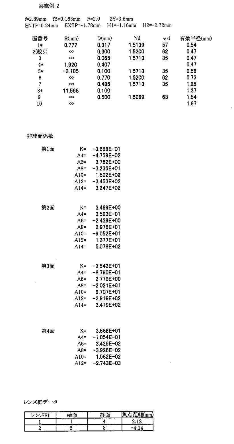
実施例2で対象とする撮像素子は、1/5インチ型、画素ピッチ1.75μm、1600×1200画素を想定している。図9は実施例2のレンズの断面図である。物体側から順に、物体側に凸の第1aレンズL1a、開口絞りS、第1レンズ基板LS1、像側に凹の第1bレンズL1bより、第1レンズブロックBK1が構成され、次に、物体側に凹の第2aレンズL2a、第2レンズ基板LS2、像側に凹の第2bレンズL2bより、第2レンズブロックBK2が構成され、最後に光学的ローパスフィルタ、赤外カットフィルタ、固体撮像素子のシールガラス等を想定した平行平板PTが設けられている。IMは撮像素子の撮像面である。また、全ての空気と接するレンズ部の面は非球面形状である。第1レンズブロックBK1は正の屈折力を有し、第2レンズブロックBK2は負の屈折力を有する。実施例2の第1aレンズ、第1bレンズ、第2aレンズ、第2bレンズは、硬化型樹脂材料で構成される。
図10は、実施例2にかかる撮像レンズの球面収差(a)、非点収差(b)、及び歪曲収差(c)の収差図である。ここで、球面収差図において、dはd線、gはg線に対する球面収差量をそれぞれ表す。また、非点収差図において、実線はサジタル面、点線はメリディオナル面をそれぞれ表す。条件式(3)けるα=8.1×10⁻⁵であり、条件式(4)における条件式f/f1=1.71であり、条件式(5)におけるν1-ν2=22である。
(+20℃温度変化時)
ここで、環境温度がプラス20度上昇した状態(40℃)での、実施例2に示す撮像レンズの曲率半径、軸上面間隔、非球面係数データを表8に示す。
(+20℃温度変化時)
ここで、環境温度がプラス20度上昇した状態(40℃)での、実施例2に示す撮像レンズの曲率半径、軸上面間隔、非球面係数データを表8に示す。
更に、実施例2において温度による屈折率ndの変化を表9に示す。これより、設計値(20℃)に対し+20℃上昇時のバックフォーカス変化量(ΔfB)は、-0.004[mm]となる。
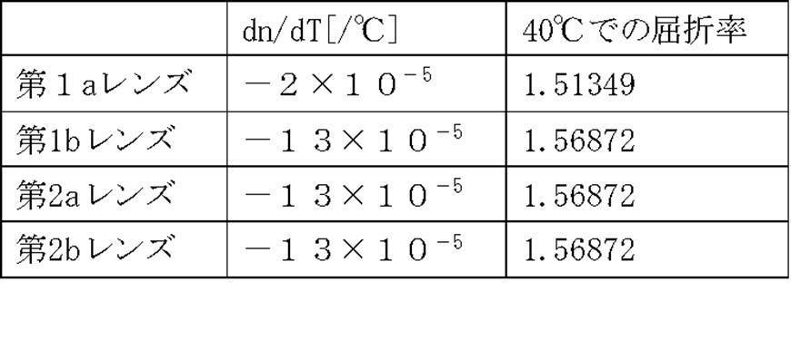
更に、実施例2においてレンズ材料を変更した場合における温度変化時の屈折率ndの別の例を表10に示す。これより、設計値(20℃)に対し+20℃上昇時のバックフォーカス変化量(ΔfB)は、-0.002[mm]となる。

更に、実施例2においてレンズ材料を変更した場合における温度変化時の屈折率ndの別の例を表11に示す。これより、設計値(20℃)に対し+20℃上昇時のバックフォーカス変化量(ΔfB)は、+0.010[mm]となる。
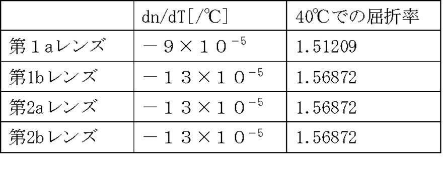
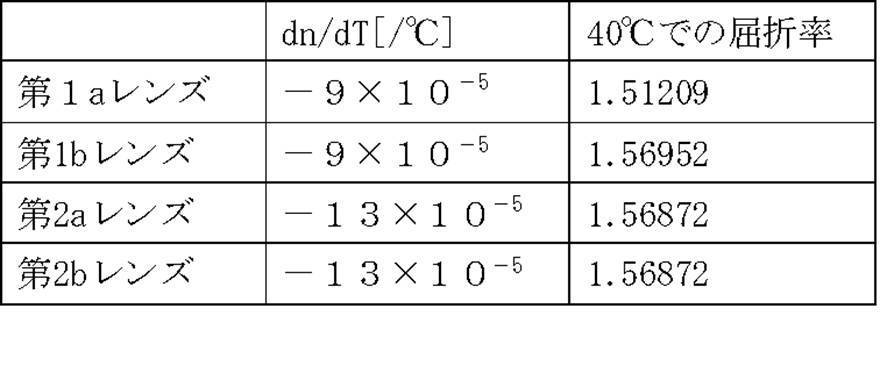
更に、実施例2においてレンズ材料を変更した場合における温度変化時の屈折率ndの別の例を表12に示す。これより、設計値(20℃)に対し+20℃上昇時のバックフォーカス変化量(ΔfB)は、+0.012[mm]となる。
一般的に焦点深度は下式で表される。
焦点深度=±Fナンバー×2×画素ピッチ
像点位置変動は、最大でも焦点深度以下にしなければならない。実施例2において想定した撮像レンズはFナンバー2.9、撮像素子は画素ピッチ1.75μmであるので、焦点深度は±0.010であり、像点位置変動は概ね焦点深度内に抑えられている。また、マイナス側への温度変化は割愛するが、像点位置はプラス側と反対符号側へ絶対値としてほぼ同等量変動する。
像点位置変動は、最大でも焦点深度以下にしなければならない。実施例2において想定した撮像レンズはFナンバー2.9、撮像素子は画素ピッチ1.75μmであるので、焦点深度は±0.010であり、像点位置変動は概ね焦点深度内に抑えられている。また、マイナス側への温度変化は割愛するが、像点位置はプラス側と反対符号側へ絶対値としてほぼ同等量変動する。
本発明によれば、大量生産性と小型化に最適な、さらには、温度上昇に伴う樹脂レンズの屈折率変化およびレンズ面の形状変化に起因するピントずれを抑えることができる撮像レンズを提供できる。携帯端末とは携帯電話機に限られない。
10 撮像レンズ
20 筐体
50 撮像装置
51 イメージセンサ
51a 光電変換部
51b 信号処理回路
52 基板
60 入力部
70 表示部
80 無線通信部
92 記憶部
100 携帯電話機
101 制御部
BK1 第1レンズブロック
BK2 第2レンズブロック
BK レンズブロック
BT ボタン
L1a 第1aレンズ
L1b 第1bレンズ
L2a 第2aレンズ
L2b 第2bレンズ
LG レンズブロック
LS1 第1レンズ基板
LS2 第2レンズ基板
PL 樹脂
PT 平行平板
S 開口絞り
SP1 第1スペーサ部材
SP2 第2スペーサ部材
UT レンズブロックユニット
UT1 第1レンズブロックユニット
UT2 第2レンズブロックユニット
20 筐体
50 撮像装置
51 イメージセンサ
51a 光電変換部
51b 信号処理回路
52 基板
60 入力部
70 表示部
80 無線通信部
92 記憶部
100 携帯電話機
101 制御部
BK1 第1レンズブロック
BK2 第2レンズブロック
BK レンズブロック
BT ボタン
L1a 第1aレンズ
L1b 第1bレンズ
L2a 第2aレンズ
L2b 第2bレンズ
LG レンズブロック
LS1 第1レンズ基板
LS2 第2レンズ基板
PL 樹脂
PT 平行平板
S 開口絞り
SP1 第1スペーサ部材
SP2 第2スペーサ部材
UT レンズブロックユニット
UT1 第1レンズブロックユニット
UT2 第2レンズブロックユニット
Claims (12)
- 平行平板であるレンズ基板と、前記レンズ基板の物体側面及び像側面の少なくとも一方に形成され、正または負のパワーを有するレンズ部とをそれぞれ備えてなり、前記レンズ部と前記レンズ基板とは屈折率とアッベ数のうち少なくとも一方が異なっており、このようなレンズ群をレンズブロックとして、前記レンズ基板の両側にレンズ部が形成された前記レンズブロックを少なくとも1個含む撮像レンズにおいて、最も物体側に配置されるレンズブロックを第1レンズブロックとし、第1レンズブロックの物体側に形成されたレンズ部を第1aレンズとするとき、
前記第1aレンズが正の屈折力を有し、以下の式を満たすことを特徴とする撮像レンズ。
-9×10⁻⁵/℃≦dn/dT(1)≦-2×10-5/℃
ただし、
dn/dT(1):第1aレンズを構成する材料の、屈折率の温度変化係数 - 前記撮像レンズは、前記レンズ基板の物体側面及び像側面上の少なくとも一方に形成される負の屈折力を有するレンズ部を有し、以下の式を満たすことを特徴とする、請求項1記載の撮像レンズ。
-14×10-5/℃≦dn/dT(N)≦-9×10-5/℃
ただし、
dn/dT(N):前記負の屈折力を有するレンズ部を構成する材料の、屈折率の温度変化係数 - 前記第1レンズブロックの像側に、所定間隔を隔て、少なくとも1つのレンズブロックが配置されることを特徴とする、請求項1又は2記載の撮像レンズ。
- 前記レンズ基板はガラス材料から形成され、前記第1aレンズの材料の線膨張係数αが次式を満たすこと特徴とする、請求項1~3のいずれかに記載の撮像レンズ。
4×10⁻⁵≦α≦10×10-5 - 下式を満たすことを特徴とする、請求項1~4のいずれかに記載の撮像レンズ。
1.0≦f/f1a≦3.0
ただし、
f:撮像レンズ全系の焦点距離(mm)
f1a:第1aレンズの空気中での焦点距離(mm) - 前記第1レンズブロックの像側に形成されたレンズ部を第1bレンズとするとき、第1bレンズは負の屈折力を有し、以下の条件式を満たすことを特徴とする、請求項1~5のいずれかに記載の撮像レンズ。
10<ν1a-ν1b<40
ただし、
ν1a:前記第1aレンズを構成する材料のアッベ数
ν1b:前記第1bレンズを構成する材料のアッベ数 - 前記第1aレンズは樹脂材料から構成されること特徴とする、請求項1~6のいずれかに記載の撮像レンズ。
- 前記第1aレンズの樹脂材料には、長さ30ナノメートル以下の無機微粒子が分散されていることを特徴とする、請求項1~7のいずれかに記載の撮像レンズ。
- 前記第1aレンズの樹脂材料は、硬化型樹脂であることを特徴とする、請求項1~8のいずれかに記載の撮像レンズ。
- 前記第1aレンズの樹脂材料は、UV硬化型樹脂であることを特徴とする、請求項1~9のいずれかに記載の撮像レンズ。
- 請求項1~10の何れかに記載の撮像レンズと、この撮像レンズで結像された物体像を光電変換するイメージセンサとを備えることを特徴とする撮像装置。
- 請求項11に記載の撮像装置を備えることを特徴とする携帯端末。
Applications Claiming Priority (2)
| Application Number | Priority Date | Filing Date | Title |
|---|---|---|---|
| JP2009-131723 | 2009-06-01 | ||
| JP2009131723 | 2009-06-01 |
Publications (1)
| Publication Number | Publication Date |
|---|---|
| WO2010140415A1 true WO2010140415A1 (ja) | 2010-12-09 |
Family
ID=43297556
Family Applications (1)
| Application Number | Title | Priority Date | Filing Date |
|---|---|---|---|
| PCT/JP2010/054202 Ceased WO2010140415A1 (ja) | 2009-06-01 | 2010-03-12 | 撮像レンズ、撮像装置及び携帯端末 |
Country Status (1)
| Country | Link |
|---|---|
| WO (1) | WO2010140415A1 (ja) |
Cited By (2)
| Publication number | Priority date | Publication date | Assignee | Title |
|---|---|---|---|---|
| JP2011081350A (ja) * | 2009-10-02 | 2011-04-21 | Visera Technologies Co Ltd | イメージ捕捉レンズモジュール |
| CN105652599A (zh) * | 2014-12-04 | 2016-06-08 | 上海微电子装备有限公司 | 降低光刻投影物镜环境热效应影响的方法 |
Citations (1)
| Publication number | Priority date | Publication date | Assignee | Title |
|---|---|---|---|---|
| WO2008102648A1 (ja) * | 2007-02-19 | 2008-08-28 | Konica Minolta Opto, Inc. | 撮像レンズ及び撮像装置並びに携帯端末 |
-
2010
- 2010-03-12 WO PCT/JP2010/054202 patent/WO2010140415A1/ja not_active Ceased
Patent Citations (1)
| Publication number | Priority date | Publication date | Assignee | Title |
|---|---|---|---|---|
| WO2008102648A1 (ja) * | 2007-02-19 | 2008-08-28 | Konica Minolta Opto, Inc. | 撮像レンズ及び撮像装置並びに携帯端末 |
Cited By (3)
| Publication number | Priority date | Publication date | Assignee | Title |
|---|---|---|---|---|
| JP2011081350A (ja) * | 2009-10-02 | 2011-04-21 | Visera Technologies Co Ltd | イメージ捕捉レンズモジュール |
| CN105652599A (zh) * | 2014-12-04 | 2016-06-08 | 上海微电子装备有限公司 | 降低光刻投影物镜环境热效应影响的方法 |
| CN105652599B (zh) * | 2014-12-04 | 2018-03-02 | 上海微电子装备(集团)股份有限公司 | 降低光刻投影物镜环境热效应影响的方法 |
Similar Documents
| Publication | Publication Date | Title |
|---|---|---|
| JP5321954B2 (ja) | 撮像レンズ、撮像装置及び携帯端末 | |
| JP5413738B2 (ja) | 撮像レンズ、撮像装置及び携帯端末 | |
| JP5311043B2 (ja) | 撮像レンズ、撮像装置、携帯端末、撮像レンズの製造方法及び撮像装置の製造方法。 | |
| JP5267825B2 (ja) | 撮像レンズ、撮像装置、デジタル機器、及び撮像レンズの製造方法 | |
| WO2009101928A1 (ja) | レンズユニット、撮像レンズ、撮像装置および携帯端末 | |
| JP2009251367A (ja) | 撮像レンズ、撮像レンズの製造方法及び撮像装置 | |
| CN101788707B (zh) | 摄像透镜、摄像装置、便携终端及摄像透镜的制造方法 | |
| CN102197329B (zh) | 摄像透镜、摄像装置及便携终端 | |
| WO2011086827A1 (ja) | 撮像レンズ、撮像装置及び携帯端末 | |
| JP5648689B2 (ja) | 撮像レンズ及び撮像装置 | |
| CN101874217B (zh) | 摄像透镜、摄像装置及便携终端 | |
| WO2012160983A1 (ja) | 撮像レンズ、撮像装置及び携帯端末 | |
| CN101939682A (zh) | 摄像透镜、摄像装置及便携终端 | |
| WO2009125654A1 (ja) | レンズブロックの製造方法、レンズブロック、撮像レンズ、撮像装置及び携帯端末 | |
| JP5267773B2 (ja) | 撮像レンズ、撮像装置、デジタル機器、及び撮像レンズの製造方法 | |
| WO2010087084A1 (ja) | 撮像レンズ、撮像装置及び携帯端末 | |
| WO2010140415A1 (ja) | 撮像レンズ、撮像装置及び携帯端末 | |
| JP2009251368A (ja) | 撮像レンズ及び撮像装置 | |
| JP2013218353A (ja) | 撮像レンズ、撮像装置及び携帯端末 | |
| WO2010146899A1 (ja) | 撮像レンズ、撮像装置及び携帯端末 | |
| JP2009204877A (ja) | 撮像レンズ及び撮像装置 | |
| JP5585471B2 (ja) | 撮像レンズ及び画像処理装置 | |
| WO2009110311A1 (ja) | 撮像レンズ、撮像装置及び撮像レンズの製造方法 |
Legal Events
| Date | Code | Title | Description |
|---|---|---|---|
| 121 | Ep: the epo has been informed by wipo that ep was designated in this application |
Ref document number: 10783201 Country of ref document: EP Kind code of ref document: A1 |
|
| NENP | Non-entry into the national phase |
Ref country code: DE |
|
| 122 | Ep: pct application non-entry in european phase |
Ref document number: 10783201 Country of ref document: EP Kind code of ref document: A1 |
|
| NENP | Non-entry into the national phase |
Ref country code: JP |