WO2010134447A1 - オフセット補償回路及びオフセット補償方法 - Google Patents
オフセット補償回路及びオフセット補償方法 Download PDFInfo
- Publication number
- WO2010134447A1 WO2010134447A1 PCT/JP2010/057951 JP2010057951W WO2010134447A1 WO 2010134447 A1 WO2010134447 A1 WO 2010134447A1 JP 2010057951 W JP2010057951 W JP 2010057951W WO 2010134447 A1 WO2010134447 A1 WO 2010134447A1
- Authority
- WO
- WIPO (PCT)
- Prior art keywords
- offset
- frequency
- frequency offset
- compensation
- component
- Prior art date
- Legal status (The legal status is an assumption and is not a legal conclusion. Google has not performed a legal analysis and makes no representation as to the accuracy of the status listed.)
- Ceased
Links
Images








Classifications
-
- H—ELECTRICITY
- H04—ELECTRIC COMMUNICATION TECHNIQUE
- H04L—TRANSMISSION OF DIGITAL INFORMATION, e.g. TELEGRAPHIC COMMUNICATION
- H04L27/00—Modulated-carrier systems
- H04L27/26—Systems using multi-frequency codes
- H04L27/2601—Multicarrier modulation systems
- H04L27/2647—Arrangements specific to the receiver only
- H04L27/2655—Synchronisation arrangements
- H04L27/2657—Carrier synchronisation
-
- H—ELECTRICITY
- H04—ELECTRIC COMMUNICATION TECHNIQUE
- H04L—TRANSMISSION OF DIGITAL INFORMATION, e.g. TELEGRAPHIC COMMUNICATION
- H04L25/00—Baseband systems
- H04L25/02—Details ; arrangements for supplying electrical power along data transmission lines
- H04L25/0264—Arrangements for coupling to transmission lines
- H04L25/0292—Arrangements specific to the receiver end
- H04L25/0296—Arrangements to ensure DC-balance
Definitions
- the present invention relates to an offset compensation circuit and an offset compensation method for compensating an offset of an OFDM (Orthogonal Frequency Division Multiplexing) signal.
- OFDM Orthogonal Frequency Division Multiplexing
- the OFDM scheme has a high transmission rate within a limited band and is resistant to multipath, and has recently been used for various wireless communications.
- g an OFDM wireless signal is used.
- Fig. 10 shows the OFDM baseband signal spectrum without DC offset and frequency offset. If the OFDM signal has no DC offset and no frequency offset, the subcarriers do not interfere with each other. Further, the center frequency of the DC subcarrier is 0 Hz.
- FIG. 11 shows an OFDM baseband signal spectrum including a DC offset and a frequency offset. Since the presence of the DC offset and the frequency offset affects the demodulation process, it is necessary to compensate for the DC offset and the frequency offset.
- the direct conversion OFDM receiver directly demodulates the RF (high frequency) signal received by the antenna to extract the I (in-phase) and Q (quadrature) components of the OFDM baseband signal, and then performs OFDM demodulation. Do.
- the frequency of the RF signal and the local oscillation signal are the same, but the level of the RF signal is not sufficient and the S / N is not good compared to the local oscillation signal.
- a DC offset occurs due to the wraparound of the component to the RF signal.
- the frequency intervals of all subcarriers are set so as to satisfy orthogonality, and the DC offset does not affect the demodulation process if it is originally.
- the oscillation frequency of the local oscillator does not completely coincide with the frequency of the RF signal and is slightly shifted, that is, it has a frequency offset. This frequency shift itself is a part of the frequency correction processing in the subsequent stage.
- the frequency error estimate is estimated larger or less than the actual one.
- a first method that first compensates for a DC offset and then compensates for a frequency offset, and first compensates for a frequency offset and then compensates for a DC offset.
- Second method for compensation see, for example, Patent Document 2
- frequency offset candidate values are obtained by singular value decomposition of a system matrix, optimal frequency offset candidate values are searched, and optimal frequency offset candidates.
- third method for estimating the DC offset from the value see, for example, Patent Document 3).
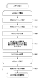
- FIG. 12 shows a flowchart of an example of a conventional OFDM signal offset compensation method (first method).
- first method a DC offset is estimated from the preamble of the OFDM signal, and the estimated DC offset is compensated.
- step S2 the frequency offset is estimated, and the estimated frequency offset is compensated.
- FIG. 13 is a flowchart showing an example of a conventional OFDM signal offset compensation method (second method).
- step S3 the frequency offset is estimated from the preamble of the OFDM signal, and the preamble frequency offset is compensated. Thereafter, in step S4, a DC offset is estimated from the preamble compensated for the frequency offset, and in step S5, the DC offset is compensated for the OFDM signal data and the frequency offset is compensated.
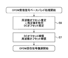
- FIG. 14 shows a flowchart of an example of a conventional OFDM signal offset compensation method (third method).
- a frequency offset candidate value is obtained by singular value decomposition of the system matrix, and the optimum frequency offset candidate value is searched by multiplying the received signal by the frequency offset candidate value in step S6.
- a DC offset is estimated from a candidate value of a large frequency offset.
- the DC offset estimated in step S7 is compensated, and the estimated frequency offset is compensated.
- the value observed as the DC offset value at the center frequency of 0 Hz includes the adjacent subcarrier component D ′.
- FIG. 15 shows an extracted subcarrier component D ′ adjacent thereto.
- the component D ′ of the adjacent subcarrier is compensated in step S1, so that interference with the adjacent subcarrier is caused as shown in FIG. There was a problem of deterioration.
- the DC offset can be accurately estimated in step S4.
- the OFDM signal includes a DC offset and a frequency offset
- the frequency offset is estimated first, an error occurs in the estimated value of the frequency offset due to the influence of the DC offset. There was a problem that the reception performance deteriorated due to the error of the estimated value.
- the present invention has been made in view of the above problems, and provides an offset compensation circuit and an offset compensation method for accurately estimating and compensating for a DC offset and a frequency offset at high speed without increasing the circuit scale. With the goal.
- an offset compensation circuit is an offset compensation circuit that estimates and compensates for a DC offset and a frequency offset of an OFDM signal, and is included in a signal obtained by orthogonally demodulating the OFDM signal.
- DC offset estimation compensation means for estimating and compensating for an offset value
- frequency offset estimation compensation means for estimating and compensating for a frequency offset value included in the signal compensated by the DC offset estimation compensation means
- the frequency offset estimation compensation Using the DC offset value estimated by the DC offset estimation compensation means and the frequency offset value estimated by the frequency offset estimation compensation means, the sub-carrier overcompensation component in the DC offset compensation means
- an offset compensation method is an offset compensation method for estimating and compensating for a DC offset and a frequency offset of an OFDM signal, and is included in a signal obtained by orthogonally demodulating the OFDM signal.
- a first step for estimating and compensating for an offset value, a second step for estimating and compensating for a frequency offset value included in the signal compensated for in the first step, and a frequency offset compensated for in the second step The third step of estimating the DC offset value from the signal, the DC offset value estimated in the third step, and the frequency offset value estimated in the second step are used.
- a compensation component is calculated, and the overcompensation component is calculated from the DC offset value estimated in the first step.
- a fourth step of removing the overcompensation component in the fourth step a fifth step of compensating the signal obtained by orthogonally demodulating the OFDM signal with the DC offset value, and a signal compensated in the fifth step. And a sixth step of compensating and outputting the included frequency offset value.
- the DC offset and the frequency offset can be compensated at high speed and with high accuracy without increasing the circuit scale.
- 5 is a flowchart of a conventional OFDM signal offset compensation method.
- 5 is a flowchart of a conventional OFDM signal offset compensation method.
- 5 is a flowchart of a conventional OFDM signal offset compensation method.
- It is a figure which shows the OFDM baseband signal spectrum for demonstrating the interference with respect to an adjacent subcarrier.
- FIG. 1 shows a block diagram of an embodiment of an OFDM receiver to which an offset compensation circuit of the present invention is applied.
- an RF signal received by an antenna 10 is amplified by a low noise amplifier (LNA) 11 and then supplied to mixers 12 and 13, respectively.
- LNA low noise amplifier
- the local oscillation signal output from the local oscillator 14 is directly supplied to the mixer 12, and is phase-shifted by ⁇ / 2 by the phase shifter 15 and supplied to the mixer 13.
- the mixers 12 and 13, the local oscillator 14, and the phase shifter 15 constitute a direct conversion type quadrature demodulator.
- the mixer 12 multiplies the RF signal and the phase-shifted local oscillation signal to output an I (in-phase) signal of the OFDM baseband signal.
- the mixer 13 multiplies the RF signal and the local oscillation signal and outputs a Q (orthogonal) signal of the OFDM baseband signal.
- the I signal output from the mixer 12 is amplified by an AGC (automatic gain control) amplifier 17, then unnecessary high frequency components are removed by a low-pass filter 18, digitized by an A / D converter 19, and sent to a digital compensation / demodulation unit 20. Supplied.
- the Q signal output from the mixer 13 is amplified by an AGC (automatic gain control) amplifier 21, then unnecessary high frequency components are removed by a low-pass filter 22, and digitized by an A / D converter 23 to be digitally compensated / demodulated. 20 is supplied.
- the digital compensation / demodulation unit 20 estimates and compensates the DC offset and the frequency offset from the I and Q signals, and then performs demodulation. That is, offset compensation is executed in the digital compensation / demodulation unit 20.
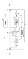
- FIG. 2 shows a block diagram of an embodiment of the offset compensation circuit of the present invention.
- the I and Q signals output from the A / D converters 19 and 23 are supplied to the multiplier 31 after passing through various blocks.
- a frequency offset value ⁇ f is supplied from a frequency offset estimation unit 38, which will be described later
- the multiplier 31 performs carrier recovery from the frequency offset ⁇ f, performs frequency offset compensation by performing complex multiplication on each of the I and Q signals, and outputs the result.
- the I and Q signals output from the multiplier 31 are supplied to a subtracter 32 and a DC offset estimation unit 33.
- FIG. 3 shows a configuration diagram of an embodiment of an OFDM radio frame in the wireless LAN standard IEEE802.11a.
- the OFDM radio frame has a PLCP preamble, a SIGNAL that is an OFDM header, and data in the data area.
- the PLCP preamble has a short training symbol that is a fixed pattern using short symbols and a long training symbol that is a fixed pattern using long symbols.
- the short training symbol has symbols S 1 to S 10 .
- the short training symbol and the long training symbol are used for synchronization, AGC, and offset estimation.
- the DC offset estimator 33 obtains a time average value of n samples of one symbol period for each of the short training symbols (eg, symbol S 7 ) of the I and Q signals, and uses this time average value to estimate the DC offset of each of the I and Q signals. Value.
- a received signal (training symbol) without a DC offset is s (t) and a DC offset is D
- a received signal r (t) having a DC offset is expressed as follows.
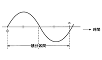
- the I and Q signals of each symbol When there is no DC offset and no frequency offset, the I and Q signals of each symbol have a time average value of 1 symbol period as shown in FIG. 4A. However, when there is a DC offset and a frequency offset, the I and Q signals of each symbol have values other than 0 for the time average value of one symbol period.
- the DC offset estimation unit 33 holds the DC offset value D 0 estimated for each of the I and Q signals and supplies it to the selector 34 and the subtracter 35.
- control unit 40 the timing of the symbol S 7 in operation stable time (e.g. short training symbols for AGC amplifier 17, 21 and other circuitry from the start of reception of the OFDM radio frame, Note that, for example, in the case of such S 5 and S 6
- the DC offset estimation unit 33 is instructed to start the DC offset estimation operation. Further, the control unit 40 causes the selector 34 to select the DC offset value D 0 output from the DC offset estimation unit 33 and supplies it to the subtracter 32.
- the subtracter 32 supplies I, to the multiplier 37 and the frequency offset estimator 38 subtracts the DC offset value D 0 for each Q signal output of the multiplier 31.
- the frequency offset estimator 38 estimates the frequency offset using the 2n-sample I and Q signals that are the next two symbols (for example, the symbols S 8 and S 9 ) after the symbol (for example, the symbol S 7 ) used for the DC offset estimation. Do.
- the frequency offset estimator 38 performs a complex correlation operation with the I and Q signals of n samples (one symbol period) before, and calculates a phase change amount with the I and Q signals n samples before, thereby calculating the frequency. Estimate the offset.
- the training symbol is a periodic signal, and the same data is repeated for each symbol interval ⁇ t, and therefore is expressed by the following equation.
- r (t) s (t) exp (j2 ⁇ ft) Since r (t) is a periodic signal, the following equation can be obtained by taking the autocorrelation for one symbol period. Note that s * represents a complex number conjugate with s.
- the frequency offset estimation unit 38 estimates the frequency offset value ⁇ f and supplies it to the overcompensation component calculation unit 36 and the switch 39.
- the control unit 40 switches the switch 39 so as to supply the multiplier 31 with the carrier regenerated from the frequency offset value ⁇ f at the next symbol (for example, the symbol S 10 ) for which the frequency offset has been estimated.
- the multiplier 31 outputs I and Q signals compensated for the frequency offset.
- the value D 0 observed as the DC offset value at the center frequency 0 Hz is adjacent to the value D 0.
- a subcarrier component D ′ is also included.
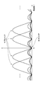
- the OFDM baseband signal spectrum compensated for the DC offset and the frequency offset is DC offset compensated up to the adjacent subcarrier component D ′, and the adjacent subcarrier is interfered (overcompensated). It is in the state.
- the DC offset estimator 33 obtains a time average value of n samples of one symbol period in the next symbol (for example, symbol S 10 ) subjected to frequency offset estimation, and uses this time average value as the DC offset of each of the I and Q signals.
- the estimated value is d ′.
- the DC offset estimated value d ′ in this case is a component caused by a component D ′ that is regarded as an offset of an adjacent subcarrier and is overcompensated.
- the control unit 40 controls the overcompensation component calculation unit 36 to supply the DC offset estimation values d ′ of the I and Q signals output from the DC offset estimation unit 33.
- the overcompensation component calculation unit 36 calculates an overcompensation component D ′, which is a component of adjacent subcarriers, using the following equation (2) based on the DC offset estimation value d ′ of each of the I and Q signals.
- f 0 is the subcarrier spacing.
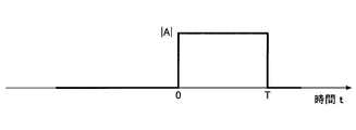
- a rectangular wave having a constant complex number A from time 0 to time T is expressed by the following equation (3).
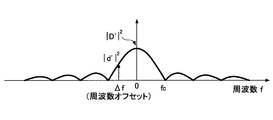
- the complex DC offset added to the OFDM signal can also be considered in the same manner as the rectangular wave represented by the above equation (3). Therefore, the frequency spectrum of the DC offset is as shown in FIG. 6C.
- Equation (2) When the above equation (5) is solved for D ′, the above equation (2) is obtained.
- the condition under which D ′ can be obtained using equation (2) is the case where d ′ is other than 0 because D ′ is calculated using the ratio to d ′.
- the overcompensation component calculation unit 36 supplies the overcompensation component D ′ of each of the I and Q signals to the subtractor 35.
- the subtracter 35 subtracts the overcompensation component D ′ from the DC offset value D 0 held and output by the DC offset estimator 33 and supplies it to the selector 34.
- Selector 34 under the control of the controller 40, for example, supplied to the subtracter 32 selects the output of the subtracter 35 is at the reception timing of the symbol S 10 and later.
- the switch 39 supplies the carrier 37 reproduced from the frequency offset value ⁇ f to the multiplier 37 under the control of the control unit 40.
- the subtractor 32 subtracts the true value D of the DC offset from each of the I and Q signals that have passed through the multiplier 31, performs DC offset compensation, and supplies the result to the multiplier 37 and the frequency offset estimation unit 38.
- This DC offset compensation is not affected by the overcompensation component D '.
- the multiplier 37 performs frequency offset compensation by performing complex multiplication of the carrier reproduced from the frequency offset ⁇ f on each of the I and Q signals, and outputs the result.
- FIG. 7 is a flowchart for explaining the operation of the offset compensation circuit according to the embodiment of the present invention.
- DC offset estimator 33 in step S11 it estimates a DC offset value D 0.
- step S12 the subtractor 32 performs DC offset compensation of the I and Q signals.
- step S13 the frequency offset estimation unit 38 estimates the frequency offset value ⁇ f.
- step S14 the multiplier 31 performs frequency offset compensation of the I and Q signals.
- step S15 the DC offset estimation unit 33 estimates the DC offset estimated value d ′.
- step S ⁇ b> 16 the overcompensation component calculation unit 36 calculates the overcompensation component D ′ using the DC offset estimation value d ′ supplied from the DC offset estimation unit 33.
- the subtractor 35 subtracts the calculated overcompensation component D ′ from the DC offset value D 0 to obtain the DC offset D, and supplies the DC offset D to the subtractor 32.
- step S17 the subtractor 32 performs DC offset compensation of the I and Q signals using the DC offset D.
- step S18 the multiplier 31 performs frequency offset compensation of the I and Q signals and outputs the result. After step S18 is executed, demodulation of the OFDM received signal is started.
- steps S13 to S17 may be executed a plurality of times, then step S18 may be executed, and then demodulation of the OFDM received signal may be started.
- FIG. 8 shows a flowchart in this case.
- steps S23 to S27 corresponding to steps S13 to S17 are repeated m times (m is an integer). That is, in step S23, the frequency offset estimation unit 38 estimates the frequency offset value ⁇ f.
- the multiplier 31 performs frequency offset compensation for the I and Q signals.
- step S25 the DC offset estimation unit 33 estimates the DC offset estimated value d ′.
- step S ⁇ b> 26 the overcompensation component calculation unit 36 calculates the overcompensation component D ′ using the DC offset estimation value d ′ supplied from the DC offset estimation unit 33.
- the subtractor 35 subtracts the overcompensation component D ′ from the DC offset value D 0 to obtain the DC offset D, and supplies the DC offset D to the subtractor 32.
- step S27 the subtractor 32 performs DC offset compensation of the I and Q signals using the DC offset D.
- step S28 corresponding to step S18, the multiplier 31 performs frequency offset compensation of the I and Q signals and outputs the result. After executing this step S28, demodulation of the OFDM received signal is started.
- the offset estimation accuracy can be further improved.
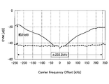
- FIG. 9 shows an EVM (Error Vector Magnitude) with respect to the frequency offset value when the DC offset and the frequency offset are compensated.
- EVM Error Vector Magnitude
- the maximum frequency used is 5.805 GHz ⁇ 232.2 kHz.
- the compensation result according to the present embodiment shows an improvement of about 25 dB relative to the compensation result according to the prior art. It turns out that it is suppressing.
- a time average is used for estimating the DC offset
- a complex correlation operation is used for estimating the frequency offset
- the calculation of the above equation (2) is added, so that the DC offset and the frequency offset with high accuracy can be obtained. Compensation can be performed.
- the multiplier 31 and the overcompensation component calculator 36 may be added as compared with the conventional example (Patent Document 1), it is not necessary to add a particularly large block. For this reason, an increase in circuit scale can be suppressed.
- the time required for the estimation of the DC offset, the estimation of the frequency offset, and the calculation of the equation (2) is four symbol periods of the short training symbol, and the DC offset and the frequency offset can be compensated at high speed.
- This embodiment has been described by taking the wireless LAN standard IEEE 802.11a, g as an example, but is not limited to the above embodiment.
- the present invention can be applied to the OFDM system adopted in the entire wireless LAN standard IEEE 802.11. Further, the present invention can be applied not only to a wireless LAN but also to general wireless communication using OFDM.
Landscapes
- Engineering & Computer Science (AREA)
- Computer Networks & Wireless Communication (AREA)
- Signal Processing (AREA)
- Power Engineering (AREA)
- Circuits Of Receivers In General (AREA)
Abstract
オフセット補償回路は、OFDM信号に含まれるDCオフセット値を推定して補償するDCオフセット推定補償手段と、前記DCオフセットを補償された信号に含まれる周波数オフセット値を推定して補償する周波数オフセット推定補償手段と、前記周波数オフセット推定補償手段で補償されたのち前記DCオフセット推定補償手段で推定されたDCオフセット値と、前記周波数オフセット推定補償手段で推定された周波数オフセット値を用いて、前記DCオフセット補償手段におけるサブキャリアの過補償成分を算出する過補償成分算出手段と、前記DCオフセット推定補償手段で推定されたDCオフセット値から前記過補償成分算出手段で算出した過補償成分を取り除いて前記DCオフセット推定補償手段でのDCオフセット補償に用いる過補償成分除去手段とを有し、過補償成分を取り除いたのちDCオフセットを補償した信号に対し周波数オフセットを補償し出力する。
Description
本発明は、OFDM(Orthogonal Frequency Division Multiplexing:直交周波数分割多重)信号のオフセットを補償するオフセット補償回路及びオフセット補償方法に関する。
OFDM方式は、制限された帯域内で高い伝送レートを有し、また、マルチパスに強いため、近年種々の無線通信に利用されている。例えば、無線LAN規格IEEE802.11a,gにおいて、OFDM方式の無線信号が使用される。
図10にDCオフセット及び周波数オフセットのないOFDMベースバンド信号スペクトラムを示す。OFDM信号にDCオフセット及び周波数オフセットがない場合は、各サブキャリアは互いに干渉することはない。また、DCサブキャリアのセンター周波数は0Hzとなる。
図11にDCオフセット及び周波数オフセットを含むOFDMベースバンド信号スペクトラムを示す。DCオフセットと周波数オフセットが存在すると復調処理に影響を及ぼすために、DCオフセットと周波数オフセットを補償する必要がある。
ここで、OFDM信号のDCオフセットと周波数オフセットについて説明する。ダイレクトコンバージョン方式のOFDM受信装置は、アンテナで受信したRF(高周波)信号を直接的に直交復調してOFDMベースバンド信号のI(同相)成分とQ(直交)成分を取り出し、その後にOFDM復調を行う。
しかし、このダイレクトコンバージョン方式では、RF信号と局部発振信号の周波数が同じであるが、局部発振信号に比べてRF信号のレベルが充分ではなくS/Nが良好とは言えないため、局部発振信号成分のRF信号への回り込み等により、DCオフセットが生じる。ただ、OFDM方式では、全てのサブキャリアの周波数間隔が直交性を満たすように設定され、上記DCオフセットは本来ならば、復調処理に影響を及ぼすことはない。ところが、局部発振器の発振周波数はRF信号の周波数と完全には一致せず僅かにずれ、つまり、周波数オフセットを有している場合が一般的であり、この周波数ずれ自体は後段の周波数補正処理部分によって補正されるものの、上記のDCオフセットがある場合は、その周波数誤差推定が実際より大きく推定されたり、少なく推定されたりする。
従来のOFDM信号のオフセット補償方法として、先にDCオフセットを補償して次に周波数オフセットを補償する第1の方法(例えば特許文献1参照)、先に周波数オフセットを補償して次にDCオフセットを補償する第2の方法(例えば特許文献2参照)、システムの行列を特異値分解して周波数オフセットの候補値を求めておき、最適な周波数オフセットの候補値を探索し、最適な周波数オフセットの候補値からDCオフセットを推定する第3の方法(例えば特許文献3参照)等がある。
図12は従来のOFDM信号のオフセット補償方法(第1の方法)の一例のフローチャートを示す。図12において、ステップS1でOFDM信号のプリアンブルからDCオフセットを推定し、推定したDCオフセットを補償する。その後、ステップS2で周波数オフセットを推定し、推定した周波数オフセットを補償する。
図13は従来のOFDM信号のオフセット補償方法(第2の方法)の一例のフローチャートを示す。図13において、ステップS3でOFDM信号のプリアンブルから周波数オフセットを推定しプリアンブルの周波数オフセットを補償する。その後、ステップS4で周波数オフセットを補償したプリアンブルからDCオフセットを推定し、ステップS5でOFDM信号のデータに対しDCオフセットを補償すると共に周波数オフセットを補償する。
図14は従来のOFDM信号のオフセット補償方法(第3の方法)の一例のフローチャートを示す。図14において、システムの行列を特異値分解して周波数オフセットの候補値を求めておき、ステップS6で受信信号に周波数オフセットの候補値を乗算して最適な周波数オフセットの候補値を探索し、最適な周波数オフセットの候補値からDCオフセットを推定する。次に、ステップS7で推定したDCオフセットを補償し、推定した周波数オフセットを補償する。
図11のOFDMベースバンド信号スペクトラムでは、センター周波数0Hzにおいて、DCオフセット値として観測される値には、隣接するサブキャリアの成分D’も含まれている。図15に隣接するサブキャリアの成分D’を抜き出して示している。
図12に示す第1の方法では、隣接するサブキャリアの成分D’までステップS1で補償されるため、図15に示すように、隣接するサブキャリアに対する干渉を引き起こしてしまい、この干渉により受信性能が劣化するという問題があった。
図13に示す第2の方法では、ステップS3で周波数オフセットが完全に補償されていれば、ステップS4でDCオフセットを正確に推定することができる。しかし、OFDM信号にDCオフセット及び周波数オフセットが含まれる場合に、先に周波数オフセットを推定すると、DCオフセットの影響で周波数オフセットの推定値に誤差が生じる。この推定値の誤差により受信性能が劣化するという問題があった。
図14に示す第3の方法では、システムの行列を特異値分解して周波数オフセットの候補値を求めるために回路規模が大きくなり算出に時間がかかる。更に、ステップS6で受信信号に周波数オフセットの候補値を乗算して最適な周波数オフセットの候補値を探索するために算出時間がかかり、リアルタイムのオフセット補償動作を行うことができないという問題があった。
本発明は、上記の課題に鑑みてなされたものであり、回路規模を増大させることなく、DCオフセット及び周波数オフセットを高速にかつ精度良く推定し補償するオフセット補償回路及びオフセット補償方法を提供することを目的とする。
上記の課題を解決するため、本発明に係るオフセット補償回路は、OFDM信号のDCオフセット及び周波数オフセットを推定して補償するオフセット補償回路であって、前記OFDM信号を直交復調した信号に含まれるDCオフセット値を推定して補償するDCオフセット推定補償手段と、前記DCオフセット推定補償手段で補償された信号に含まれる周波数オフセット値を推定して補償する周波数オフセット推定補償手段と、前記周波数オフセット推定補償手段で補償されたのち前記DCオフセット推定補償手段で推定されたDCオフセット値と、前記周波数オフセット推定補償手段で推定された周波数オフセット値を用いて、前記DCオフセット補償手段におけるサブキャリアの過補償成分を算出する過補償成分算出手段と、前記DCオフセット推定補償手段で推定されたDCオフセット値から前記過補償成分算出手段で算出した過補償成分を取り除いて前記DCオフセット推定補償手段でのDCオフセット補償に用いる過補償成分除去手段とを有し、前記過補償成分を取り除いたのち前記DCオフセット推定補償手段でDCオフセットを補償した信号に対し前記周波数オフセット推定補償手段で周波数オフセットを補償し出力することを特徴とする。
上記の課題を解決するため、本発明に係るオフセット補償方法は、OFDM信号のDCオフセット及び周波数オフセットを推定して補償するオフセット補償方法であって、前記OFDM信号を直交復調した信号に含まれるDCオフセット値を推定して補償する第1ステップと、前記第1ステップで補償された信号に含まれる周波数オフセット値を推定して補償する第2ステップと、前記第2ステップで周波数オフセットを補償された信号からDCオフセット値を推定する第3ステップと、前記第3ステップで推定されたDCオフセット値と、前記第2ステップで推定された周波数オフセット値を用いて、前記第1ステップにおけるサブキャリアの過補償成分を算出し、前記第1ステップで推定されたDCオフセット値から前記過補償成分を取り除く第4ステップと、前記第4ステップで前記過補償成分を取り除いたDCオフセット値で前記OFDM信号を直交復調した信号の補償を行う第5ステップと、前記第5ステップで補償された信号に含まれる周波数オフセット値を補償し出力する第6ステップとを有することを特徴とする。
本発明に係るオフセット補償回路及びオフセット補償方法によれば、回路規模を増大させることなく、DCオフセット及び周波数オフセットを高速かつ精度良く補償することができる。
以下、本発明を実施するための形態について、添付図面を参照しながら説明する。
図1は、本発明のオフセット補償回路を適用したOFDM受信機の一実施形態のブロック構成図を示す。図1において、アンテナ10で受信したRF信号はローノイズアンプ(LNA)11で増幅されたのち、ミキサ12,13それぞれに供給される。
局部発振器14が出力する局部発振信号は直接ミキサ12に供給されると共に、移相器15でπ/2移相されてミキサ13に供給される。ミキサ12,13と局部発振器14と移相器15はダイレクトコンバージョン方式の直交復調器を構成している。ミキサ12はRF信号と移相された局部発振信号を乗算してOFDMベースバンド信号のI(同相)信号を出力する。ミキサ13はRF信号と局部発振信号を乗算してOFDMベースバンド信号のQ(直交)信号を出力する。
ミキサ12の出力するI信号はAGC(自動利得制御)アンプ17で増幅されたのち、ローパスフィルタ18で不要高周波成分を除去され、A/Dコンバータ19でデジタル化されてデジタル補償・復調部20に供給される。また、ミキサ13の出力するQ信号はAGC(自動利得制御)アンプ21で増幅されたのち、ローパスフィルタ22で不要高周波成分を除去され、A/Dコンバータ23でデジタル化されてデジタル補償・復調部20に供給される。
デジタル補償・復調部20はI,Q信号からDCオフセット及び周波数オフセットの推定及び補償を行い、その後、復調を行う。すなわち、デジタル補償・復調部20内においてオフセット補償が実行される。
<オフセット補償回路>
図2は、本発明のオフセット補償回路の一実施形態のブロック構成図を示す。図2において、A/Dコンバータ19,23が出力するI,Q信号は各種ブロックを通過したのち乗算器31に供給される。乗算器31は後述する周波数オフセット推定部38から周波数オフセット値Δfを供給された場合、この周波数オフセットΔfからキャリア再生を行い、I,Q信号それぞれに複素乗算することで周波数オフセット補償を行って出力する。乗算器31の出力するI,Q信号は減算器32及びDCオフセット推定部33に供給される。
図2は、本発明のオフセット補償回路の一実施形態のブロック構成図を示す。図2において、A/Dコンバータ19,23が出力するI,Q信号は各種ブロックを通過したのち乗算器31に供給される。乗算器31は後述する周波数オフセット推定部38から周波数オフセット値Δfを供給された場合、この周波数オフセットΔfからキャリア再生を行い、I,Q信号それぞれに複素乗算することで周波数オフセット補償を行って出力する。乗算器31の出力するI,Q信号は減算器32及びDCオフセット推定部33に供給される。
ここで、図3に、無線LAN規格IEEE802.11aにおけるOFDM無線フレームの一実施形態の構成図を示す。OFDM無線フレームはPLCPプリアンブル、OFDMヘッダであるSIGNAL、データ領域のDataを有している。PLCPプリアンブルはショートシンボルによる固定パターンであるショートトレーニングシンボルと、ロングシンボルによる固定パターンであるロングトレーニングシンボルを有している。ショートトレーニングシンボルはシンボルS1~S10を有している。ショートトレーニングシンボル及びロングトレーニングシンボルは、同期、AGC、オフセット推定に用いられる。
なお、本実施形態では1シンボルの周期をn回(例えば、n=16)サンプリングして、それぞれI,Q信号がA/Dコンバータ19,23から供給されている。
DCオフセット推定部33は、I,Q信号それぞれのショートトレーニングシンボル(例えばシンボルS7)について1シンボル周期のnサンプルの時間平均値を求め、この時間平均値をI,Q信号それぞれのDCオフセット推定値とする。
具体的には、DCオフセットのない受信信号(トレーニングシンボル)をs(t)、DCオフセットをDとすると、DCオフセットの存在する受信信号r(t)は次のように表される。
r(t)=s(t)+D
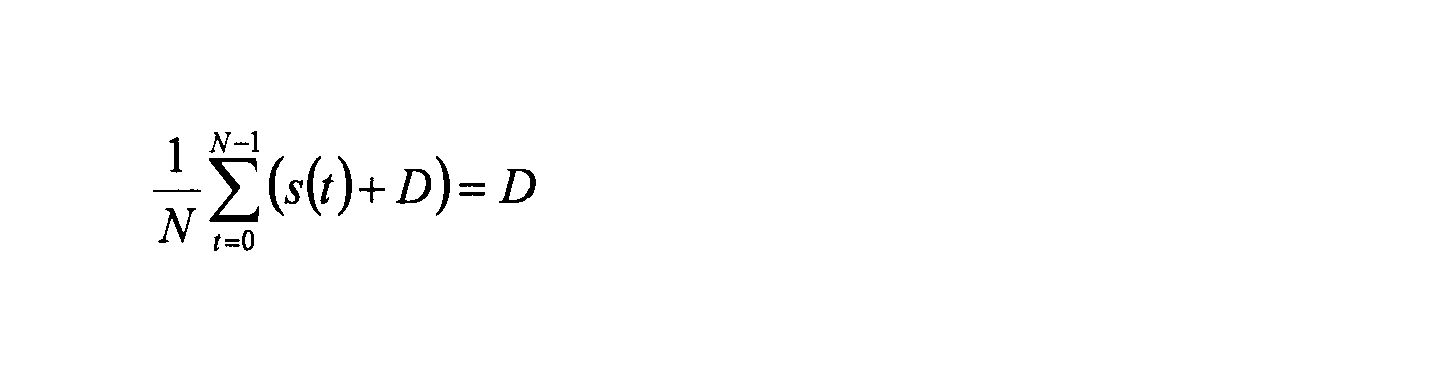
ここで、トレーニングシンボルであるs(t)は直流成分がない周期信号であるため1シンボル区間の平均値は0となる。従って、r(t)を1シンボル区間(Nサンプル)で平均をとると、次式によりDCオフセットを求めることができる。
ここで、トレーニングシンボルであるs(t)は直流成分がない周期信号であるため1シンボル区間の平均値は0となる。従って、r(t)を1シンボル区間(Nサンプル)で平均をとると、次式によりDCオフセットを求めることができる。
なお、DCオフセット及び周波数オフセットがない場合には、各シンボルのI,Q信号は図4Aに示すように1シンボル周期の時間平均値が0となる。しかし、DCオフセット及び周波数オフセットがある場合には各シンボルのI,Q信号は1シンボル周期の時間平均値は0以外の値となる。DCオフセット推定部33はI,Q信号それぞれで推定したDCオフセット値D0を保持し、セレクタ34及び減算器35に供給する。
ところで、制御部40はOFDM無線フレームの受信開始からAGCアンプ17,21やその他回路の動作が安定した時点(例えばショートトレーニングシンボルのシンボルS7のタイミング、なお、例えばS5やS6等の場合もある)でDCオフセット推定部33にDCオフセット推定動作の開始を指示している。また、制御部40はDCオフセット推定部33の出力するDCオフセット値D0をセレクタ34に選択させて減算器32に供給する。
減算器32は乗算器31の出力するI,Q信号それぞれについてDCオフセット値D0を減算して乗算器37及び周波数オフセット推定部38に供給する。
周波数オフセット推定部38はDCオフセット推定に用いたシンボル(例えばシンボルS7)の次の2シンボル(例えばシンボルS8,S9)である2nサンプルのI,Q信号を用いて周波数オフセットの推定を行う。周波数オフセット推定部38はnサンプル(1シンボル周期)前のサンプルのI,Q信号との複素相関演算を行って、nサンプル前のI,Q信号との位相変化量を算出し、それにより周波数オフセットを推定する。
具体的には、周波数オフセットのない受信信号(トレーニングシンボル)をs(t)とすると、トレーニングシンボルは周期信号であり、1シンボル区間Δt毎に同じデータが繰り返されるので次式で表される。
s(t)=s(t-Δt)
また、周波数オフセットΔfのある信号r(t)は次式で表される。
また、周波数オフセットΔfのある信号r(t)は次式で表される。
r(t)=s(t)exp(j2πΔft)
また、r(t)は周期信号であるため、1シンボル区間の自己相関をとると、次式を得ることができる。なお、s*はsと共役な複素数を表す。
また、r(t)は周期信号であるため、1シンボル区間の自己相関をとると、次式を得ることができる。なお、s*はsと共役な複素数を表す。
r(t)s*(t-Δt)=|s(t)|2exp(j2πΔfΔt)
この式における位相Δωは次式で表される。
この式における位相Δωは次式で表される。
Δω=arg|s(t)|2exp(j2πΔfΔt)
従って、周波数オフセットΔfは以下のように表せる。
従って、周波数オフセットΔfは以下のように表せる。
Δf=Δω/2πΔt
なお、周波数オフセットがある場合には各シンボルのI,Q信号は図4Bに示すように見かけ上の1シンボル周期が変化し、現在のサンプルと1シンボル周期前のサンプルとの相関が低くなる。周波数オフセット推定部38は周波数オフセット値Δfを推定して過補償成分算出部36及びスイッチ39に供給する。
なお、周波数オフセットがある場合には各シンボルのI,Q信号は図4Bに示すように見かけ上の1シンボル周期が変化し、現在のサンプルと1シンボル周期前のサンプルとの相関が低くなる。周波数オフセット推定部38は周波数オフセット値Δfを推定して過補償成分算出部36及びスイッチ39に供給する。
制御部40は、周波数オフセット推定を行った次のシンボル(例えばシンボルS10)で周波数オフセット値Δfから再生されたキャリアを乗算器31に供給するようスイッチ39の切替えを行う。これにより、乗算器31は周波数オフセットを補償したI,Q信号を出力する。
ここで、先に説明したように、DCオフセット及び周波数オフセットを含むOFDM信号では、図11及び図15に示すように、センター周波数0Hzにおいて、DCオフセット値として観測される値D0には、隣接するサブキャリアの成分D’も含まれている。なお、DCオフセットの真値をDとすると、下記の(1)式の関係となる。
D0=D+D’ …(1)
このため、DCオフセット及び周波数オフセットを補償したOFDMベースバンド信号スペクトラムは図5に示すように、隣接するサブキャリアの成分D’までDCオフセット補償されて、隣接するサブキャリアが干渉(過補償)された状態である。
このため、DCオフセット及び周波数オフセットを補償したOFDMベースバンド信号スペクトラムは図5に示すように、隣接するサブキャリアの成分D’までDCオフセット補償されて、隣接するサブキャリアが干渉(過補償)された状態である。
DCオフセット推定部33は、周波数オフセット推定を行った次のシンボル(例えばシンボルS10)において、1シンボル周期のnサンプルの時間平均値を求め、この時間平均値をI,Q信号それぞれのDCオフセット推定値d’とする。この場合のDCオフセット推定値d’は、図5に示すように、隣接するサブキャリアのオフセットとみなされ過補償された成分D’に起因する成分である。制御部40はDCオフセット推定部33の出力するI,Q信号それぞれのDCオフセット推定値d’を過補償成分算出部36に供給させるよう制御する。
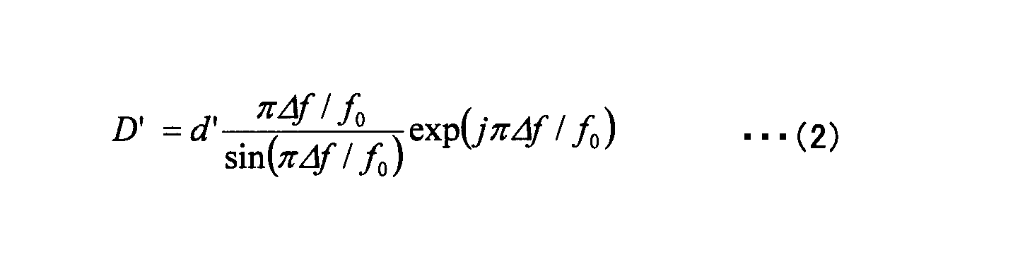
過補償成分算出部36は、I,Q信号それぞれのDCオフセット推定値d’に基づき、下記の(2)式を用いて隣接するサブキャリアの成分である過補償成分D’を算出する。ここで、f0はサブキャリア間隔である。


次に、上記の(4)式をDCオフセット算出の式に置き換える。このため、上記の(4)式にT=1/f0,AT=D’,f=Δfを代入すると、下記の(5)式が得られる。
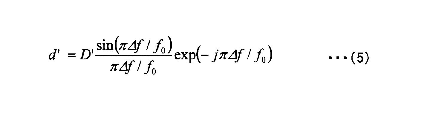
図2に戻って説明するに、過補償成分算出部36はI,Q信号それぞれの過補償成分D’は減算器35に供給される。減算器35は、DCオフセット推定部33が保持して出力するDCオフセット値D0から過補償成分D’を減算してセレクタ34に供給する。セレクタ34は制御部40の制御により、例えばシンボルS10以降の受信タイミングでは減算器35の出力を選択して減算器32に供給する。また、スイッチ39は制御部40の制御により周波数オフセット値Δfから再生されたキャリアを乗算器37に供給する。
これにより、減算器32は、乗算器31を通過したI,Q信号それぞれからDCオフセットの真値Dを減算してDCオフセット補償を行って乗算器37及び周波数オフセット推定部38に供給する。このDCオフセット補償では過補償成分D’の影響を受けていない。そして、乗算器37は周波数オフセットΔfから再生されたキャリアをI,Q信号それぞれに複素乗算することで周波数オフセット補償を行って出力する。
次に、図7は、本発明の一実施形態に係るオフセット補償回路の動作を説明するためのフローチャートである。図7のフローチャートにおいて、ステップS11でDCオフセット推定部33は、DCオフセット値D0を推定する。ステップS12で減算器32は、I,Q信号のDCオフセット補償を行う。
続いて、ステップS13で周波数オフセット推定部38は、周波数オフセット値Δfの推定を行う。ステップS14で乗算器31は、I,Q信号の周波数オフセット補償を行う。
この後、ステップS15でDCオフセット推定部33は、DCオフセット推定値d’を推定する。ステップS16で過補償成分算出部36は、DCオフセット推定部33から供給されるDCオフセット推定値d’を用いて過補償成分D’を算出する。減算器35は、DCオフセット値D0から、算出された過補償成分D’を減算してDCオフセットDを求め、DCオフセットDを減算器32に供給する。
この後、ステップS17で減算器32は、DCオフセットDを用いてI,Q信号のDCオフセット補償を行う。ステップS18で乗算器31は、I,Q信号の周波数オフセット補償を行って出力する。このステップS18が実行されたのち、OFDM受信信号の復調が開始される。
ところで、上記のステップS12を実行したのち、ステップS13~S17を複数回実行したのちステップS18を実行し、そののちOFDM受信信号の復調を開始してもよい。図8は、この場合のフローチャートを示す。図8のフローチャートにおいて、上記のステップS12を実行したのち、ステップS13~S17に対応するステップS23~S27をm回(mは整数)ループして繰り返す。即ち、ステップS23で周波数オフセット推定部38は、周波数オフセット値Δfの推定を行う。ステップS24で乗算器31は、I,Q信号の周波数オフセット補償を行う。
この後、ステップS25でDCオフセット推定部33は、DCオフセット推定値d’を推定する。ステップS26で過補償成分算出部36は、DCオフセット推定部33から供給されるDCオフセット推定値d’を用いて過補償成分D’を算出する。また、減算器35は、DCオフセット値D0から過補償成分D’を減算してDCオフセットDを求め、DCオフセットDを減算器32に供給する。この後、ステップS27で減算器32は、DCオフセットDを用いてI,Q信号のDCオフセット補償を行う。最後に、ステップS18に対応するステップS28で乗算器31は、I,Q信号の周波数オフセット補償を行って出力する。このステップS28を実行したのちOFDM受信信号の復調が開始される。
このように、図7の一部の処理を図8のように複数回実行することにより、オフセット推定精度をより向上させることができる。
図9にDCオフセット及び周波数オフセットの補償を行った場合の周波数オフセット値に対するEVM(Error Vector Magnitude)を示す。これは無線LAN規格IEEE802.11aに基づくシミュレーション結果である。ここで、実線は従来技術による補償結果を示し、黒丸付の一点鎖線は本実施形態による補償結果を示す。
無線LAN規格IEEE802.11aでは使用する最大周波数は5.805GHz±232.2kHzである。図9に示すように、周波数オフセット-232.2kHzにおいて、本実施形態による補償結果は、従来技術による補償結果に対し約25dBの改善が見られ、本実施形態では周波数オフセットに対しEVMの劣化を抑制していることが分かる。
本実施形態ではDCオフセットの推定には時間平均を用い、周波数オフセットの推定には複素相関演算を用い、上記の(2)式の演算を追加することで、精度の高いDCオフセット及び周波数オフセットの補償を行うことができる。また、従来例(特許文献1)と比較して追加するブロックは乗算器31と過補償成分算出部36でよいため、特別に大きなブロックを追加する必要がない。このため、回路規模の増大を抑えることができる。上記のDCオフセットの推定、周波数オフセットの推定、上記の(2)式の演算に要する時間は、ショートトレーニングシンボルの4シンボル周期であり、DCオフセット及び周波数オフセットを高速に補償することができる。
本実施形態は無線LAN規格IEEE802.11a,gを一例として説明してきたが、上記の実施形態に限定されない。無線LAN規格IEEE802.11全般において採用されるOFDM方式に適用することができる。また、無線LANに限らずOFDMを用いた無線通信一般にも適用することができる。
本国際出願は、2009年5月19日に出願された日本国特許出願2009-120483号に基づく優先権を主張するものであり、日本国特許出願2009-120483号の全内容を本国際出願に援用する。
Claims (4)
- OFDM信号のDCオフセット及び周波数オフセットを推定して補償するオフセット補償回路であって、
前記OFDM信号を直交復調した信号に含まれるDCオフセット値を推定して補償するDCオフセット推定補償手段と、
前記DCオフセット推定補償手段で補償された信号に含まれる周波数オフセット値を推定して補償する周波数オフセット推定補償手段と、
前記周波数オフセット推定補償手段で補償されたのち前記DCオフセット推定補償手段で推定されたDCオフセット値と、前記周波数オフセット推定補償手段で推定された周波数オフセット値を用いて、前記DCオフセット補償手段におけるサブキャリアの過補償成分を算出する過補償成分算出手段と、
前記DCオフセット推定補償手段で推定されたDCオフセット値から前記過補償成分算出手段で算出した過補償成分を取り除いて前記DCオフセット推定補償手段でのDCオフセット補償に用いる過補償成分除去手段と、
を有し、
前記過補償成分を取り除いたのち前記DCオフセット推定補償手段でDCオフセットを補償した信号に対し前記周波数オフセット推定補償手段で周波数オフセットを補償し出力することを特徴とするオフセット補償回路。 - 請求項1記載のオフセット補償回路において、
前記過補償成分算出手段は、前記周波数オフセット値をΔfとし、前記DCオフセット推定値をd’とし、前記過補償成分をD’とし、サブキャリア間隔をf0として、下記の式

- OFDM信号のDCオフセット及び周波数オフセットを推定して補償するオフセット補償方法であって、
前記OFDM信号を直交復調した信号に含まれるDCオフセット値を推定して補償する第1ステップと、
前記第1ステップで補償された信号に含まれる周波数オフセット値を推定して補償する第2ステップと、
前記第2ステップで周波数オフセットを補償された信号からDCオフセット値を推定する第3ステップと、
前記第3ステップで推定されたDCオフセット値と、前記第2ステップで推定された周波数オフセット値を用いて、前記第1ステップにおけるサブキャリアの過補償成分を算出し、前記第1ステップで推定されたDCオフセット値から前記過補償成分を取り除く第4ステップと、
前記第4ステップで前記過補償成分を取り除いたDCオフセット値で前記OFDM信号を直交復調した信号の補償を行う第5ステップと、
前記第5ステップで補償された信号に含まれる周波数オフセット値を補償し出力する第6ステップと、
を有することを特徴とするオフセット補償方法。 - 請求項3記載のオフセット補償方法において、
前記第2乃至第5ステップを複数回繰り返すことを特徴とするオフセット補償方法。
Applications Claiming Priority (2)
| Application Number | Priority Date | Filing Date | Title |
|---|---|---|---|
| JP2009120483A JP5387126B2 (ja) | 2009-05-19 | 2009-05-19 | オフセット補償回路及びオフセット補償方法 |
| JP2009-120483 | 2009-05-19 |
Publications (1)
| Publication Number | Publication Date |
|---|---|
| WO2010134447A1 true WO2010134447A1 (ja) | 2010-11-25 |
Family
ID=43126128
Family Applications (1)
| Application Number | Title | Priority Date | Filing Date |
|---|---|---|---|
| PCT/JP2010/057951 Ceased WO2010134447A1 (ja) | 2009-05-19 | 2010-05-11 | オフセット補償回路及びオフセット補償方法 |
Country Status (2)
| Country | Link |
|---|---|
| JP (1) | JP5387126B2 (ja) |
| WO (1) | WO2010134447A1 (ja) |
Cited By (1)
| Publication number | Priority date | Publication date | Assignee | Title |
|---|---|---|---|---|
| CN105119698A (zh) * | 2015-09-14 | 2015-12-02 | 东南大学 | 非平坦信道下dco-ofdm直流偏置和功率联合优化方法 |
Citations (2)
| Publication number | Priority date | Publication date | Assignee | Title |
|---|---|---|---|---|
| US20030133518A1 (en) * | 2002-01-11 | 2003-07-17 | Rf Micro Devices | Estimation and correction of DC offset in the presence of frequency offset |
| JP2008236704A (ja) * | 2006-05-16 | 2008-10-02 | Sony Corp | 無線通信装置 |
-
2009
- 2009-05-19 JP JP2009120483A patent/JP5387126B2/ja active Active
-
2010
- 2010-05-11 WO PCT/JP2010/057951 patent/WO2010134447A1/ja not_active Ceased
Patent Citations (2)
| Publication number | Priority date | Publication date | Assignee | Title |
|---|---|---|---|---|
| US20030133518A1 (en) * | 2002-01-11 | 2003-07-17 | Rf Micro Devices | Estimation and correction of DC offset in the presence of frequency offset |
| JP2008236704A (ja) * | 2006-05-16 | 2008-10-02 | Sony Corp | 無線通信装置 |
Cited By (2)
| Publication number | Priority date | Publication date | Assignee | Title |
|---|---|---|---|---|
| CN105119698A (zh) * | 2015-09-14 | 2015-12-02 | 东南大学 | 非平坦信道下dco-ofdm直流偏置和功率联合优化方法 |
| CN105119698B (zh) * | 2015-09-14 | 2018-03-20 | 东南大学 | 非平坦信道下dco‑ofdm直流偏置和功率联合优化方法 |
Also Published As
| Publication number | Publication date |
|---|---|
| JP2010272901A (ja) | 2010-12-02 |
| JP5387126B2 (ja) | 2014-01-15 |
Similar Documents
| Publication | Publication Date | Title |
|---|---|---|
| CN101406017B (zh) | 用于在正交频分复用系统中估计并补偿载波频率偏移的方法和设备 | |
| US6625111B1 (en) | OFDM communication apparatus | |
| US7457366B2 (en) | System and method for adaptive phase compensation of OFDM signals | |
| US8594210B2 (en) | Method and apparatus for positioning an FFT-window in an OFDM-receiver | |
| CN100448184C (zh) | 正交频分多路复用系统的接收机 | |
| KR101468514B1 (ko) | 통신 시스템에서의 잔류 주파수 에러를 추정하는 방법 및 장치 | |
| JP2010525710A (ja) | Ofdm受信機におけるiqインバランス補正方法及び装置 | |
| CN1300947C (zh) | 移动通信系统中补偿频率偏移的装置和方法 | |
| JP4279027B2 (ja) | Ofdm復調方法及び半導体集積回路 | |
| JP5342449B2 (ja) | Cfo、dcoのひずみ量推定方法およびこれを用いた受信信号補正方法、受信装置 | |
| JP5387126B2 (ja) | オフセット補償回路及びオフセット補償方法 | |
| JP2004007439A (ja) | 無線伝送装置 | |
| JP3558879B2 (ja) | ディジタル通信装置 | |
| US20050180518A1 (en) | Preamble for estimation and equalization of asymmetries between inphase and quadrature branches in multicarrier transmission systems | |
| JP3495962B2 (ja) | 歪み推定装置 | |
| JP3945623B2 (ja) | 周波数同期方法及びこれを用いたofdm受信装置 | |
| KR101314776B1 (ko) | 이동통신 시스템에서 주파수 옵셋을 보상하기 위한 장치 및방법 | |
| JP4861796B2 (ja) | 無線通信装置及び通信処理回路 | |
| JP2002290371A (ja) | 直交周波数分割多重伝送信号受信装置 | |
| JPH11331120A (ja) | 搬送波周波数同期回路 | |
| JP2004088662A (ja) | 直交マルチキャリア信号伝送方式のシンボル同期タイミング検出方法および装置 | |
| KR100813399B1 (ko) | Zero-if 수신기의 i/q부정합 보상 장치 및 그 방법 | |
| JP2004064439A (ja) | マルチキャリア受信装置 | |
| JP2002164865A (ja) | Ofdm通信装置 | |
| JP2004088661A (ja) | 直交マルチキャリア信号伝送方式の周波数オフセット推定方法および装置 |
Legal Events
| Date | Code | Title | Description |
|---|---|---|---|
| 121 | Ep: the epo has been informed by wipo that ep was designated in this application |
Ref document number: 10777680 Country of ref document: EP Kind code of ref document: A1 |
|
| NENP | Non-entry into the national phase |
Ref country code: DE |
|
| 122 | Ep: pct application non-entry in european phase |
Ref document number: 10777680 Country of ref document: EP Kind code of ref document: A1 |