WO2010131683A1 - アンテナ装置 - Google Patents
アンテナ装置 Download PDFInfo
- Publication number
- WO2010131683A1 WO2010131683A1 PCT/JP2010/058058 JP2010058058W WO2010131683A1 WO 2010131683 A1 WO2010131683 A1 WO 2010131683A1 JP 2010058058 W JP2010058058 W JP 2010058058W WO 2010131683 A1 WO2010131683 A1 WO 2010131683A1
- Authority
- WO
- WIPO (PCT)
- Prior art keywords
- antenna
- magnetic sheet
- antenna coil
- coil
- antenna module
- Prior art date
- Legal status (The legal status is an assumption and is not a legal conclusion. Google has not performed a legal analysis and makes no representation as to the accuracy of the status listed.)
- Ceased
Links
Images



Classifications
-
- G—PHYSICS
- G06—COMPUTING OR CALCULATING; COUNTING
- G06K—GRAPHICAL DATA READING; PRESENTATION OF DATA; RECORD CARRIERS; HANDLING RECORD CARRIERS
- G06K19/00—Record carriers for use with machines and with at least a part designed to carry digital markings
- G06K19/06—Record carriers for use with machines and with at least a part designed to carry digital markings characterised by the kind of the digital marking, e.g. shape, nature, code
- G06K19/067—Record carriers with conductive marks, printed circuits or semiconductor circuit elements, e.g. credit or identity cards also with resonating or responding marks without active components
- G06K19/07—Record carriers with conductive marks, printed circuits or semiconductor circuit elements, e.g. credit or identity cards also with resonating or responding marks without active components with integrated circuit chips
- G06K19/077—Constructional details, e.g. mounting of circuits in the carrier
- G06K19/07749—Constructional details, e.g. mounting of circuits in the carrier the record carrier being capable of non-contact communication, e.g. constructional details of the antenna of a non-contact smart card
-
- H—ELECTRICITY
- H01—ELECTRIC ELEMENTS
- H01Q—ANTENNAS, i.e. RADIO AERIALS
- H01Q1/00—Details of, or arrangements associated with, antennas
- H01Q1/12—Supports; Mounting means
- H01Q1/22—Supports; Mounting means by structural association with other equipment or articles
- H01Q1/2208—Supports; Mounting means by structural association with other equipment or articles associated with components used in interrogation type services, i.e. in systems for information exchange between an interrogator/reader and a tag/transponder, e.g. in Radio Frequency Identification [RFID] systems
- H01Q1/2225—Supports; Mounting means by structural association with other equipment or articles associated with components used in interrogation type services, i.e. in systems for information exchange between an interrogator/reader and a tag/transponder, e.g. in Radio Frequency Identification [RFID] systems used in active tags, i.e. provided with its own power source or in passive tags, i.e. deriving power from RF signal
-
- H—ELECTRICITY
- H01—ELECTRIC ELEMENTS
- H01Q—ANTENNAS, i.e. RADIO AERIALS
- H01Q7/00—Loop antennas with a substantially uniform current distribution around the loop and having a directional radiation pattern in a plane perpendicular to the plane of the loop
Definitions
- the present invention relates to an antenna device that receives a magnetic field transmitted from a transmitter and is inductively coupled with the transmitter to enable communication.
- the present application includes Japanese Patent Application No. 2009-115389 filed on May 12, 2009 in Japan and Japanese Patent Application No. 2009-153630 filed on June 29, 2009 in Japan. On the basis of the above, and are incorporated into the present application by reference to these applications.
- antenna module for RFID (Radio Frequency Identification)
- a coil pattern is created on a plane using an FPC (Flexible Printed Circuit) or a rigid substrate.
- FPC Flexible Printed Circuit
- a coil is formed by winding a round wire.
- an FPC, FFC (Flexible Flat Cable) or the like is used as a harness, and the harness is formed in a ring shape to form a coil.
- the above-described antenna module is appropriately selected by a design that takes into account the arrangement and shape of components, and is used by being incorporated in an electronic device.
- an antenna module When an antenna module is placed in an electronic device, it is made of ferrite with a relatively high permeability and low loss factor so as not to be affected by the metal used in the metal casing and internal parts of the electronic device.
- the magnetic sheet is attached to the periphery of the antenna (Patent Document 1).
- Patent Document 1 a magnetic sheet made of ferrite with good magnetic properties is placed so as to overlap the antenna module, so that the magnetic field enters the metal placed around the antenna module and becomes an eddy current. To prevent it from changing.
- the ferrite magnetic sheet has been optimized in shape, combination, etc. so as to obtain good communication performance.
- the antenna module be as thin as possible while being bonded to a ferrite magnetic sheet.
- magnetic material such as ferrite is used for the purpose of preventing the generation of eddy current and heat in the electronic device on the antenna substrate formed by making the antenna planar with a flexible electronic material such as FPC.
- a seat may be attached.
- the antenna can be thinned from a dimensional viewpoint by reducing the thickness of the ferrite constituent layer, the adhesive constituent layer, and the FPC layer.
- the antenna pattern and magnetic properties are affected by the influence of the metal casing.
- the distance between the sheets is preferably as far as possible. For example, as shown in FIG.
- the present invention has been proposed in view of such circumstances, and an object of the present invention is to provide an antenna device that is thinned as a whole while maintaining communication characteristics.
- the present invention provides an antenna substrate in which an antenna coil that receives a magnetic field transmitted from a transmitter and is inductively coupled to the transmitter to enable communication is mounted on the surface of the insulating layer;
- the antenna substrate includes a magnetic sheet that is bonded to the surface of the insulating layer on which the antenna coil is not mounted via an adhesive layer and draws a magnetic field transmitted from the transmitter into the antenna coil.
- the antenna coil is used as a member for separating the antenna coil and the magnetic sheet.
- An insulating portion that is surface-mounted can be used, and good communication characteristics can be realized while reducing the overall thickness.
- FIG. 1 is a diagram showing a configuration of a wireless communication system in which an antenna module to which the present invention is applied is incorporated.
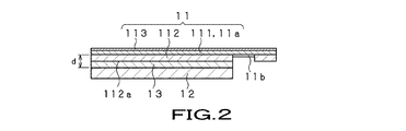
- FIG. 2 is a cross-sectional view for explaining the configuration of the antenna module to which the present invention is applied.
- FIG. 3 is a cross-sectional view for explaining the configuration of the antenna module according to the comparative example.
- FIG. 4 is a diagram for explaining a change in communication characteristics according to the distance between the antenna coil and the magnetic sheet.
- 5A and 5B are diagrams showing specific dimensions of the antenna module.
- FIG. 6 is a diagram for explaining measurement conditions for measuring the communication distance.
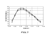
- FIG. 7 is a diagram for explaining communication characteristics when the reader / writer and the antenna module are inductively coupled.
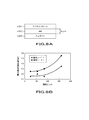
- FIG. 8A and FIG. 8B are diagrams for explaining a change in communication characteristics according to the interval between the antenna pattern and the magnetic sheet.
- An antenna module to which the present invention is applied is a device that is in a communicable state by electromagnetic induction generated with a transmitter that transmits electromagnetic waves.
- the antenna module for RFID Radio Frequency Identification
- the wireless communication system 100 includes an antenna module 1 to which the present invention is applied, and a reader / writer 2 that accesses the antenna module 1.
- the reader / writer 2 functions as a transmitter that transmits a magnetic field to the antenna module 1, and specifically, an antenna 2a that transmits a magnetic field toward the antenna module 1, and an antenna that is inductively coupled via the antenna 2a.
- a control board 2b that communicates with the module 1 is provided. That is, the reader / writer 2 is provided with a control board 2b electrically connected to the antenna 2a.
- a control circuit composed of electronic components such as one or a plurality of integrated circuit chips is mounted on the control board 2b. The control circuit executes various processes based on the data received from the antenna module 1.
- the control circuit when writing data to the antenna module 1, the control circuit encodes the data, modulates a carrier wave of a predetermined frequency (for example, 13.56 MHz) based on the encoded data, and amplifies the modulated modulation signal Then, the antenna 2a is driven by the amplified modulation signal. Further, when reading data from the antenna module 1, the control circuit amplifies the modulation signal of the data received by the antenna 2a, demodulates the modulation signal of the amplified data, and decodes the demodulated data.
- a coding method and a modulation method used in a general reader / writer are used. For example, a Manchester coding method or an ASK (Amplitude Shift Keying) modulation method is used.
- the antenna module 1 incorporated in the housing 3 of the electronic device is used to draw the magnetic field into the antenna coil 11a and the antenna substrate 11 on which the antenna coil 11a capable of communicating with the reader / writer 2 that is inductively coupled is mounted.
- substrate 11 is provided.
- a communication processing unit 4 that performs communication with the reader / writer 2 by a current flowing through the antenna coil 11a is incorporated in an electronic device in which the antenna module 1 is incorporated.
- the antenna coil 11a When the antenna coil 11a receives a magnetic field transmitted from the reader / writer 2, the antenna coil 11a is magnetically coupled to the reader / writer 2 by inductive coupling, receives the modulated electromagnetic wave, and performs communication processing on the received signal via the terminal portion 11b. Supply to part 4.
- the magnetic sheet 12 is formed at a position overlapping the antenna substrate 11, and draws the magnetic field transmitted from the reader / writer 2 into the antenna coil 11a. Specifically, the magnetic sheet 12 has a magnetic field in order to suppress a metal part provided inside the housing 3 of the portable electronic device from rebounding a magnetic field transmitted from the reader / writer 2 or generating an eddy current.
- the structure is pasted on the opposite side of the direction from which the light is emitted.
- the communication processing unit 4 is driven by a current flowing through the antenna coil 11 a and performs communication with the reader / writer 2. Specifically, the communication processing unit 4 demodulates the received modulation signal, decodes the demodulated data, and writes the decoded data in the internal memory of the communication processing unit 4.
- the communication processing unit 4 reads data to be transmitted to the reader / writer 2 from the internal memory, encodes the read data, modulates a carrier wave based on the encoded data, and is magnetically coupled by inductive coupling.
- the modulated radio wave is transmitted to the reader / writer 2 through the coil 11a.
- the antenna module 1 according to the present embodiment is configured as shown in FIG.
- the antenna substrate 11 is a double-access type wiring board that can be connected to the conductive wire from both the upper and lower surfaces.
- the surface of the insulating layer 112 made of polyimide has high conductivity.
- a conductive metal layer 111 made of Cu or the like, and a corrosion-resistant metal layer 113 having corrosion resistance such as Au / Ni covering the conductive metal layer 111 are sequentially laminated.
- the above-described antenna coil 11a is mounted on the surface of the insulating layer 112 by performing a patterning process or the like on the conductive metal layer 111 and the corrosion-resistant metal layer 113.
- the magnetic sheet 12 is made of a magnetic material such as a ferrite plate that has a small loss factor and can efficiently draw a magnetic field into the antenna coil 11a, and is a surface of the insulating layer 112 on the antenna substrate 11 on which the antenna coil 11a is not mounted. 112a is bonded via an insulating adhesive layer 13 such as ADH.
- the antenna module 1 is provided with a terminal portion 11b electrically connected to the antenna coil 11a on the surface 112a side of the insulating layer 112 on which the antenna coil 11a of the antenna substrate 11 is not mounted. In the antenna module 1, the antenna coil 11a and the communication processing unit 4 are electrically connected through the terminal unit 11b.
- the terminal portion 11b is made of Au / Ni having high conductivity.
- the magnetic sheet 12 is bonded to the surface 112a of the insulating layer 112 on which the antenna coil 11a of the antenna substrate 11 is not mounted via the adhesive layer 13. Therefore, in the antenna module 1, the adhesive layer 13 and the insulating layer 112 function as a member defined by a thickness d for separating the antenna coil 11a and the magnetic sheet 12 from each other.
- the antenna module 1 can use the insulating layer 112 on which the antenna coil 11a is surface-mounted as a member defined by the thickness d for separating the antenna coil 11a and the magnetic sheet 12 from each other. Good communication characteristics can be realized while reducing the overall thickness.
- the communication processing unit 4 is arranged inside the magnetic sheet to which the antenna substrate 11 is bonded, and the communication processing unit 4 and the antenna coil 11a.
- the terminal portion 11b is provided on the magnetic sheet 12 side to electrically connect the antenna module 1 to the antenna module 200 using a single access wiring board according to a comparative example as shown in FIG.
- the overall thickness can be reduced. That is, as shown in FIG. 3, the antenna module 200 is obtained by bonding a single access wiring board 210 that can be connected to a conductive wire from only one side, and a magnetic sheet 230 via an adhesive layer 220.
- a conductive metal layer 212 made of Cu having high conductivity and a resist layer 213 made of an insulating member covering the conductive metal layer 211 are sequentially laminated on the surface of the insulating layer 211 made of polyimide.
- the resist layer 213 is provided with a terminal portion 213a made of Au / Ni that is opened by etching and can be electrically connected to the conductive metal layer 212.
- the adhesive layer 220, the resist layer 213, the conductive layer are used based on the surface of the magnetic sheet 230.
- the conductive metal layer 212 and the insulating layer 211 are stacked in this order, and the resist layer 213 is provided with a terminal portion 213a.
- the adhesive layer 220 and the resist layer 213 function as members defined by a thickness d for separating the antenna coil 11a and the magnetic sheet 230 from each other.
- the antenna module 200 configured as described above differs from the antenna module 1 according to the present embodiment in that the insulating layer 211 functions as a member defined by a thickness d for separating the antenna coil 11a and the magnetic sheet 230 from each other. Because it does not, it becomes thick as a whole.
- the antenna module 1 can be made thinner as a whole module than the antenna module 200. Further, unlike the antenna module 200, the antenna module 1 is not subjected to a resist treatment using an insulating material on the antenna coil 11a mounted on the surface of the insulating layer 112, but when it is incorporated into an electronic device or the like. From the viewpoint of communicating with the reader / writer 2, no conductive member such as an electronic circuit is disposed in the space from the housing 3 to the antenna coil 11a, so that the entire module can be made thin and function as the antenna coil 11a. Can do.
- the inventors of the present application arrange the antenna module 1 so that the distance between the antenna coil and the magnetic sheet is separated within a range of 50 [ ⁇ m] to 55 [ ⁇ m] based on the following example.
- the module as a whole can be made thinner and have better communication characteristics than the antenna module 200.
- Example ⁇ Changes in communication characteristics according to antenna coil-magnetic sheet> A change in communication characteristics according to the distance between the antenna coil and the magnetic sheet will be described with reference to FIG.
- FIG. 4 shows changes in the Q value calculated by the following equation (1) when the distance between the antenna coil 11a and the magnetic sheet 12 is changed from 20 to 140 [ ⁇ m] in the antenna module 1.
- FIG. 4 shows changes in the Q value calculated by the following equation (1) when the distance between the antenna coil 11a and the magnetic sheet 12 is changed from 20 to 140 [ ⁇ m] in the antenna module 1.
- ⁇ [rad / s] is an angular frequency of the antenna coil 11a
- L [ ⁇ H] is an inductance value of the antenna coil 11a
- R [ ⁇ ] is a resistance value of the antenna coil 11a.
- the Q value is an index for evaluating communication characteristics, and the larger this value is, the better the communication sensitivity is and the larger the maximum communicable distance is.
- the conductive metal layer constituting the antenna coil 11a has a film thickness of 35 [ ⁇ m]
- the antenna substrate 101 has an outer shape of 36 [mm] ⁇ 29 [mm] and a thickness of 0.09 [mm] as shown in FIG. Part 103 is implemented.
- the antenna coil 102 has a conductor wire having a width of 0.31 [mm], a space of 0.12 [mm] between adjacent conductors, that is, a pattern pitch of 0.42 [mm], and the number of windings. It is wound to be 4.
- the magnetic sheet 104 is disposed so as to coincide with the outer shape of the antenna coil 102, and as shown in FIG.
- the shape is a substantially rectangular shape of 36 [mm] ⁇ 29 [mm].
- the magnetic sheet is a ferrite plate having a relative complex permeability of the following value in a magnetic field with an oscillation frequency of 13.56 MHz. That is, a ferrite plate having a relative complex permeability with a real part ⁇ ′ of 119 and an imaginary part ⁇ ′′ of 1.33 is used.
- the thickness of the entire module is approximately the same, and the antenna module A corresponding to the antenna module 1 as an example and the antenna module B corresponding to the antenna module 200 as a comparative example are as follows. Created in. ⁇ Antenna module A> The antenna module A uses the following double access type wiring board.
- a conductive metal layer made of Cu having a thickness of 50 ⁇ m is laminated on the surface of an insulating layer made of polyimide having a thickness of 25 ⁇ m.
- the thickness of the adhesive layer is adjusted so that the distance between the antenna coil and the magnetic sheet is 55 [ ⁇ m], and the insulating layer of the antenna substrate and the magnetic sheet are adhered.
- the antenna module B uses the following single access type wiring board. That is, a conductive metal layer made of Cu having a thickness of 35 ⁇ m and a resist layer having a thickness of 15 ⁇ m are sequentially laminated on the surface of an insulating layer made of polyimide having a thickness of 25 ⁇ m.
- the thickness of the adhesive layer is adjusted so that the distance between the antenna coil and the magnetic sheet is 50 [ ⁇ m], and the resist layer of the antenna substrate and the magnetic sheet are adhered.
- FPC is the total thickness of the antenna substrate
- interval is the interval between the antenna coil and the magnetic sheet
- Total is the total thickness of the entire module.
- the “possible distance” is a value indicating the maximum distance at which the communication between the reader / writer and the antenna module can be performed at an oscillation frequency of 13.56 [MHz]. The larger this value, the better the communication characteristics. Specifically, as shown in FIG.
- the “maximum communicable distance” is an antenna module 302 having an antenna substrate 302a using a non-contact IC card reader / writer 301 of model name RC-S440C manufactured by Sony Corporation. Measured under the condition that a 50 ⁇ 100 [mm] stainless steel plate 303 is installed as a pseudo electronic substrate at a position 2 mm away from the magnetic sheet 302b.
- the antenna module A has the same overall thickness as the antenna substrate and the module compared to the antenna module B, but the distance between the antenna coil and the magnetic sheet can be made as large as possible. As a result, communication was possible as far as 3 [mm].
- the horizontal axis represents the frequency of the magnetic field used for communication
- the vertical axis represents the maximum communicable distance corresponding to the frequency. Note that the frequency of the magnetic field transmitted from the reader / writer is 13.56 MHz as described above. However, when communication is performed by inductive coupling, communication is performed using a magnetic field component having a frequency higher than 13.56 MHz. Is done.
- the antenna module A has higher characteristics and better communication sensitivity than the antenna module B in all frequency bands to be measured. Table 2 below shows the inductance value L, resistance value R, and Q value for the antenna modules A and B.
- the antenna module A can reduce the resistance value of the antenna coil by increasing the thickness of the conductive metal layer as compared with the antenna module B. As a result, the entire antenna module can be reduced. The overall thickness was the same, and the communication performance was improved as indicated by the Q value.
- the antenna module according to the present embodiment is arranged under the condition that the distance between the antenna coil and the magnetic sheet is spaced within the range of 50 [ ⁇ m] to 55 [ ⁇ m]. As a result, the module as a whole can be reduced in thickness and have good communication characteristics. In this way, the module as a whole can be made thin and have good communication characteristics because the insulating portion on which the antenna coil is surface-mounted can be used as a member for separating the antenna coil and the magnetic sheet. .
Landscapes
- Engineering & Computer Science (AREA)
- Computer Hardware Design (AREA)
- Microelectronics & Electronic Packaging (AREA)
- Physics & Mathematics (AREA)
- General Physics & Mathematics (AREA)
- Theoretical Computer Science (AREA)
- Details Of Aerials (AREA)
- Near-Field Transmission Systems (AREA)
Abstract
通信特性を維持しつつ、全体で薄型化が図られたアンテナ装置を提供する。本発明は、リーダライタ(2)から発信される磁界を受けて、リーダライタ(2)と誘導結合されて通信可能となるアンテナコイル(11a)が、絶縁層(112)の表面に実装されたアンテナ基板(11)と、アンテナ基板(11)のアンテナコイル(11a)が実装されていない絶縁層(112)の面(112a)に、接着層(13)を介して接着され、リーダライタ(2)から発信される磁界をアンテナコイル(11a)に引き込む磁性シート(12)とを含んで構成されている。
Description
本発明は、発信器から発信される磁界を受けて、当該発信器と誘導結合されて通信可能となるアンテナ装置に関する。
本出願は、日本国において2009年5月12日に出願された日本特許出願番号特願2009-115389、及び日本国において2009年6月29日に出願された日本特許出願番号特願2009-153630を基礎として優先権を主張するものであり、これらの出願を参照することにより、本出願に援用される。
本出願は、日本国において2009年5月12日に出願された日本特許出願番号特願2009-115389、及び日本国において2009年6月29日に出願された日本特許出願番号特願2009-153630を基礎として優先権を主張するものであり、これらの出願を参照することにより、本出願に援用される。
RFID(Radio Frequency Identification)用のアンテナモジュールとして、次のような数種類のものが従来から用いられている。第1に、FPC(Flexible Printed Circuit)やリジット基板を用いてコイルパターンを平面上に作成したアンテナモジュールがある。第2に、丸線を巻き線にしてコイルを作成したアンテナモジュールがある。第3に、FPCやFFC(Flexible Flat Cable)などをハーネスにして、そのハーネスをリング状にしてコイルを形成したアンテナモジュールがある。
上述したアンテナモジュールは、部品の配置、形状を考慮した設計により、適宜選択されて、電子機器に組み込まれて使用されている。
電子機器内にアンテナモジュールを配置する場合、電子機器の金属製筐体や内部部品に使用されている金属の影響を受けないようにするため、透磁率が比較的高く、損失係数が小さいフェライト製の磁性シートをアンテナの周辺に取り付けている(特許文献1)。
このようにして、磁気特性が良好なフェライト製の磁性シートは、アンテナモジュールに重畳するように配置することによって、磁界がアンテナモジュールの周囲に配置されている金属内に入り渦電流となって熱に変わることを防ぐ。また、フェライト製の磁性シートは、良好な通信性能が得られるように、形状や組合せ等の最適化が行われている。また、携帯電話機などの携帯型電子機器の薄型化が進む中で、アンテナモジュールは、フェライト製の磁性シートと貼り合わされた状態で、できるだけ薄くなるようにすることが望まれる。
上述したアンテナモジュールは、部品の配置、形状を考慮した設計により、適宜選択されて、電子機器に組み込まれて使用されている。
電子機器内にアンテナモジュールを配置する場合、電子機器の金属製筐体や内部部品に使用されている金属の影響を受けないようにするため、透磁率が比較的高く、損失係数が小さいフェライト製の磁性シートをアンテナの周辺に取り付けている(特許文献1)。
このようにして、磁気特性が良好なフェライト製の磁性シートは、アンテナモジュールに重畳するように配置することによって、磁界がアンテナモジュールの周囲に配置されている金属内に入り渦電流となって熱に変わることを防ぐ。また、フェライト製の磁性シートは、良好な通信性能が得られるように、形状や組合せ等の最適化が行われている。また、携帯電話機などの携帯型電子機器の薄型化が進む中で、アンテナモジュールは、フェライト製の磁性シートと貼り合わされた状態で、できるだけ薄くなるようにすることが望まれる。
上述したように、アンテナをFPCなどの可撓性のある電子材料で平面形状にして作成したアンテナ基板に、電子機器内での渦電流や熱の発生を防止する目的で、フェライト製などの磁性シートが取り付けられる場合がある。
アンテナを寸法的観点から薄くするには、フェライト構成層、粘着構成層そしてFPC層各々を薄くすることによって対応できるが、通信特性の観点では、金属筐体の影響を受けるため、アンテナパターンと磁性シート間の距離ができるだけ離れていることが好ましい。例えば、図8Aに示すように、アンテナパターン401と磁性シート402を接着させるADH層403の厚みを変数d[μm]として変化させた場合、図8Bに示すように、dが小さいほど通信可能距離が小さくなってしまう。これは、アンテナパターンと磁性シート間に形成されるADH層の厚みを薄くするとアンテナ抵抗が上昇し通信性能を劣化するからである。このように、単に各部材を薄くすると通信特性が劣化してしまうという問題があった。
そこで、本発明は、このような実情に鑑みて提案されたものであり、通信特性を維持しつつ、全体で薄型化が図られたアンテナ装置を提供することを目的とする。
アンテナを寸法的観点から薄くするには、フェライト構成層、粘着構成層そしてFPC層各々を薄くすることによって対応できるが、通信特性の観点では、金属筐体の影響を受けるため、アンテナパターンと磁性シート間の距離ができるだけ離れていることが好ましい。例えば、図8Aに示すように、アンテナパターン401と磁性シート402を接着させるADH層403の厚みを変数d[μm]として変化させた場合、図8Bに示すように、dが小さいほど通信可能距離が小さくなってしまう。これは、アンテナパターンと磁性シート間に形成されるADH層の厚みを薄くするとアンテナ抵抗が上昇し通信性能を劣化するからである。このように、単に各部材を薄くすると通信特性が劣化してしまうという問題があった。
そこで、本発明は、このような実情に鑑みて提案されたものであり、通信特性を維持しつつ、全体で薄型化が図られたアンテナ装置を提供することを目的とする。
上述した課題を解決するため、本発明は、発信器から発信される磁界を受けて、発信器と誘導結合されて通信可能となるアンテナコイルが、絶縁層の表面に実装されたアンテナ基板と、アンテナ基板のアンテナコイルが実装されていない絶縁層の面に、接着層を介して接着され、発信器から発信される磁界をアンテナコイルに引き込む磁性シートとを含んで構成される。
本発明は、アンテナ基板のアンテナコイルが実装されていない絶縁層の面に、接着層を介して、磁性シートが接着されているので、アンテナコイル-磁性シート間を離間する部材として、アンテナコイルが表面実装される絶縁部を用いることができ、全体の薄型化を図りつつ良好な通信特性を実現することができる。
本発明は、アンテナ基板のアンテナコイルが実装されていない絶縁層の面に、接着層を介して、磁性シートが接着されているので、アンテナコイル-磁性シート間を離間する部材として、アンテナコイルが表面実装される絶縁部を用いることができ、全体の薄型化を図りつつ良好な通信特性を実現することができる。
以下、本発明を実施するための形態について、図面を参照しながら詳細に説明する。なお、本発明は、以下の実施形態のみに限定されるものではなく、本発明の要旨を逸脱しない範囲内において種々の変更が可能であることは勿論である。
本発明が適用されたアンテナモジュールは、電磁波を発信する発信器との間で発生する電磁誘導により通信可能状態となる装置であって、例えば図1に示すようなRFID(Radio Frequency Identification)用の無線通信システム100に組み込まれて使用される。
無線通信システム100は、本発明が適用されたアンテナモジュール1と、アンテナモジュール1に対するアクセスを行うリーダライタ2とからなる。
リーダライタ2は、アンテナモジュール1に対して磁界を発信する発信器として機能し、具体的には、アンテナモジュール1に向けて磁界を発信するアンテナ2aと、アンテナ2aを介して誘導結合されたアンテナモジュール1と通信を行う制御基板2bとを備える。
すなわち、リーダライタ2は、アンテナ2aと電気的に接続された制御基板2bが配設されている。この制御基板2bには、一又は複数の集積回路チップ等の電子部品からなる制御回路が実装されている。この制御回路は、アンテナモジュール1から受信されたデータに基づいて、各種の処理を実行する。例えば、制御回路は、アンテナモジュール1にデータを書き込む場合、データを符号化し、符号化したデータに基づいて、所定の周波数(例えば、13.56MHz)の搬送波を変調し、変調した変調信号を増幅し、増幅した変調信号でアンテナ2aを駆動する。また、制御回路は、アンテナモジュール1からデータを読み出す場合、アンテナ2aで受信されたデータの変調信号を増幅し、増幅したデータの変調信号を復調し、復調したデータを復号する。なお、制御回路では、一般的なリーダライタで用いられる符号化方式及び変調方式が用いられ、例えば、マンチェスタ符号化方式やASK(Amplitude Shift Keying)変調方式が用いられている。
電子機器の筐体3内部に組み込まれるアンテナモジュール1は、誘導結合されたリーダライタ2との間で通信可能となるアンテナコイル11aが実装されたアンテナ基板11と、磁界をアンテナコイル11aに引き込むためアンテナ基板11と重畳する位置に形成された磁性シート12とを備える。また、アンテナモジュール1が組み込まれる電子機器内部には、アンテナコイル11aに流れる電流により、リーダライタ2との間で通信を行う通信処理部4が組み込まれている。
アンテナ基板11には、例えばフレキシブルフラットケーブルなどの可撓性の導線をパターンニング処理などをすることによって形成されるアンテナコイル11aと、アンテナコイル11aと通信処理部4とを電気的に接続する端子部11bとが実装されている。
アンテナコイル11aは、リーダライタ2から発信される磁界を受けると、リーダライタ2と誘導結合によって磁気的に結合され、変調された電磁波を受信して、端子部11bを介して受信信号を通信処理部4に供給する。
磁性シート12は、アンテナ基板11と重畳する位置に形成され、リーダライタ2から発信される磁界をアンテナコイル11aに引き込む。具体的に、磁性シート12は、携帯型電子機器の筐体3内部に設けられた金属部品がリーダライタ2から発信される磁界を跳ね返したり、渦電流を発生するのを抑制するために、磁界が放射されてくる方向の反対側に貼り付けた構造をとる。
通信処理部4は、アンテナコイル11aに流れる電流により駆動し、リーダライタ2との間で通信を行う。具体的に、通信処理部4は、受信された変調信号を復調し、復調したデータを復号して、復号したデータを、当該通信処理部4が有する内部メモリに書き込む。また、通信処理部4は、リーダライタ2に送信するデータを内部メモリから読み出し、読み出したデータを符号化し、符号化したデータに基づいて搬送波を変調し、誘導結合によって磁気的に結合されたアンテナコイル11aを介して変調された電波をリーダライタ2に送信する。
以上のような構成からなる無線通信システム100において、以下では、アンテナモジュール1の構成に注目して説明する。
本実施形態に係るアンテナモジュール1では、モジュール全体の薄型化を図りつつ良好な通信特性を実現する観点から、図2に示すような構成となっている。
すなわち、アンテナ基板11は、上下両面から導線と接続可能なダブルアクセス型の配線板であり、具体的には、図2に示すように、ポリイミドからなる絶縁層112の表面に、導電性が高いCu等からなる導電性金属層111、導電性金属層111を被覆するAu/Niなどの耐腐食性を有する耐腐食性金属層113が順に積層されたものである。このような構成からなるアンテナ基板11では、導電性金属層111、耐腐食性金属層113に対して、パターンニング処理等を施すことで、絶縁層112の表面に上述したアンテナコイル11aが実装される。
磁性シート12は、例えばフェライト板などの、損失係数が小さくアンテナコイル11aに磁界を効率よく引き込むことが可能な磁性材料からなり、アンテナ基板11のアンテナコイル11aが実装されていない絶縁層112の面112aに、ADHなどの絶縁性の接着層13を介して接着されている。
また、アンテナモジュール1は、アンテナ基板11のアンテナコイル11aが実装されていない絶縁層112の面112aの側に、アンテナコイル11aと電気的に接続される端子部11bが設けられている。アンテナモジュール1は、端子部11bを介して、アンテナコイル11aと通信処理部4とが電気的に接続される。具体的には、端子部11bは、導電性が高いAu/Niから形成されている。
以上のような構成からなるアンテナモジュール1は、アンテナ基板11のアンテナコイル11aが実装されていない絶縁層112の面112aに、接着層13を介して、磁性シート12が接着されている。したがって、アンテナモジュール1では、接着層13と絶縁層112とが、アンテナコイル11a-磁性シート12間を離間するための厚みdで定義される部材として機能する。このようにして、アンテナモジュール1は、アンテナコイル11a-磁性シート12間を離間するための厚みdで定義される部材として、アンテナコイル11aが表面実装される絶縁層112を用いることができるので、全体の薄型化を図りつつ良好な通信特性を実現することができる。
特に、リーダライタ2側から発信される磁界の影響を受けないようにするため、アンテナ基板11が接着された磁性シートの内側に通信処理部4を配置して、通信処理部4とアンテナコイル11aとを電気的に接続するため磁性シート12側に端子部11bを設ける場合、アンテナモジュール1は、図3に示すような比較例に係るシングルアクセス型の配線板を用いたアンテナモジュール200に比べて全体の薄型化を図ることができる。
すなわち、アンテナモジュール200は、図3に示すように、片面のみから導線と接続可能なシングルアクセス配線板210と、接着層220を介して、磁性シート230とを接着させたものである。シングルアクセス配線板210は、ポリイミドからなる絶縁層211の表面に、導電性が高いCuからなる導電性金属層212、導電性金属層211を被覆する絶縁部材からなるレジスト層213が順に積層されたものである。なお、レジスト層213には、エッチング処理により開口され、導電性金属層212と電気的に接続可能なAu/Niからなる端子部213aが形成されている。このアンテナモジュール200では、磁性シート230側からアンテナモジュール200の導電性金属層212と通信処理部との接続を確保するため、磁性シート230の面を基準として、接着層220、レジスト層213、導電性金属層212、絶縁層211という順に積層され、レジスト層213に端子部213aが設けられた構造となっている。アンテナモジュール200では、接着層220とレジスト層213とが、アンテナコイル11a-磁性シート230間を離間するための厚みdで定義される部材として機能する。
以上のような構成からなるアンテナモジュール200は、本実施形態に係るアンテナモジュール1と異なり、絶縁層211が、アンテナコイル11a-磁性シート230間を離間するための厚みdで定義される部材として機能しないため、全体として厚くなってしまう。したがって、アンテナコイル-磁性シート間の間隔を同一の条件にした場合、アンテナモジュール1は、アンテナモジュール200に比べて、モジュール全体としての薄型化を図ることができる。
また、アンテナモジュール1は、アンテナモジュール200と異なり、絶縁層112の表面に実装されたアンテナコイル11aには、絶縁材料を用いたレジスト処理が施されていないが、電子機器等に組み込まれる際には、リーダライタ2と通信を行う観点から、筐体3からアンテナコイル11aまでの空間に電子回路等の導電部材が配置されないので、モジュール全体の薄型化を図りつつ、アンテナコイル11aとして機能させることができる。
特に、本願の発明者らは、下記の実施例に基づき、アンテナコイル-磁性シート間の間隔が50[μm]乃至55[μm]の範囲内で離間するように配置することで、アンテナモジュール1が、アンテナモジュール200に比べて、モジュール全体としての薄型化、良好な通信特性を実現することを見出した。
実施例
<アンテナコイル-磁性シート間に応じた通信特性の変化>
アンテナコイル-磁性シート間の間隔に応じた通信特性の変化について、図4を参照して説明する。図4は、アンテナモジュール1において、アンテナコイル11aと磁性シート12の間の距離を20~140[μm]まで変化させたときの、下記の(1)式で算出されるQ値の変化を示す図である。
Q=ωL/R ・・・(1)
ここで、ω[rad/s]はアンテナコイル11aの角周波数であり、L[μH]はアンテナコイル11aのインダクタンス値であり、R[Ω]はアンテナコイル11aの抵抗値である。Q値は、通信特性を評価する指標であって、この値が大きいほど通信感度が良く、最大通信可能距離が大きくなることを示す。
また、図4において、アンテナコイル11aを構成する導電性金属層は、膜厚が35[μm]であり、μ”=1、5、10は、それぞれフェライト製の磁性シート12の複素比透磁率の虚数部である。
図4では、アンテナコイル-磁性シート間の間隔が50[μm]より近づけると、Qが大きく劣化することを示している。すなわち、この間隔を狭くしてアンテナモジュール全厚を薄くすることは特性劣化を招くことを示唆している。これに対して、アンテナコイル-磁性シート間の間隔を50~55[μm]よりも厚くするとQ値は上がり、図4に示すように100[μm]程度以上で安定するが、薄型化の観点から好ましくない。
したがって、モジュール全体としての薄型化、良好な通信特性を実現する観点から、アンテナコイル-磁性シート間の間隔を50乃至55[μm]の範囲内で変化させることを制約条件として、下記のようなアンテナモジュールを具体的に作成した。
<アンテナモジュールの設計条件>
以下では、図5A及び図5Bに示すようなアンテナ基板101を用いてアンテナモジュールを作成するものとする。
すなわち、アンテナ基板101は、図5Aに示すように、外形形状が36[mm]×29[mm]、厚さが0.09[mm]であって、次のようなアンテナコイル102と、端子部103とが実装される。また、アンテナコイル102は、幅が0.31[mm]の導線が、隣接する導線間で0.12[mm]のスペース、すなわち、パターンピッチが0.42[mm]で、巻き線数が4となるように巻回される。
磁性シート104は、アンテナコイル102の外形形状と一致するように配置されるものであって、図5Bに示すように、その形状が、36[mm]×29[mm]の略矩形である。また、磁性シートは、発振周波数が13.56MHzの磁界における比複素透磁率が次の値のフェライト板を用いるものとする。すなわち、フェライト板は、比複素透磁率の実数部μ’が119、虚数部μ”が1.33のものを用いるものとする。
上述した設計条件に従い、それぞれモジュール全体の厚みが同程度となるようにして、実施例としてアンテナモジュール1に対応するアンテナモジュールAと、比較例としてアンテナモジュール200に対応するアンテナモジュールBを次のように作成した。
<アンテナモジュールA>
アンテナモジュールAは、次のようなダブルアクセス型の配線板を用いたものである。すなわち、膜厚が25μmのポリイミドからなる絶縁層の表面に、膜厚が50μmのCuからなる導電性金属層が積層されたものである。アンテナモジュールAは、アンテナコイル-磁性シート間の間隔が55[μm]となるように接着層の厚みを調整して、アンテナ基板の絶縁層と磁性シートを接着させたものである。
<アンテナモジュールB>
アンテナモジュールBは、次のようなシングルアクセス型の配線板を用いたものである。すなわち、膜厚が25μmのポリイミドからなる絶縁層の表面に、膜厚が35μmのCuからなる導電性金属層、膜厚が15μmからなるレジスト層が順に積層されたものである。アンテナモジュールBは、アンテナコイル-磁性シート間の間隔が50[μm]となるように接着層の厚みを調整して、アンテナ基板のレジスト層と磁性シートを接着させたものである。
<評価>
上述したアンテナモジュールA、Bについて、形状と通信特性とを、下記の表1を用いて評価した。ここで、「FPC」とは、アンテナ基板の全厚であり、「間隔」とは、アンテナコイル-磁性シート間の間隔であり、「Total」とはモジュール全体の全厚であり、「最大通信可能距離」とは、発振周波数が13.56[MHz]において、リーダライタとアンテナモジュール間で通信可能な最大距離を示す値であり、この値が大きいほど通信特性が良い。具体的に、「最大通信可能距離」は、図6に示すように、ソニー株式会社製の型名RC-S440Cの非接触ICカードリーダ/ライタ301を用いて、アンテナ基板302aを有するアンテナモジュール302の磁性シート302b側に2mm離れた位置に、擬似的な電子基板として50×100[mm]のステンレス板303を設置した条件下で測定したものである。
本発明が適用されたアンテナモジュールは、電磁波を発信する発信器との間で発生する電磁誘導により通信可能状態となる装置であって、例えば図1に示すようなRFID(Radio Frequency Identification)用の無線通信システム100に組み込まれて使用される。
無線通信システム100は、本発明が適用されたアンテナモジュール1と、アンテナモジュール1に対するアクセスを行うリーダライタ2とからなる。
リーダライタ2は、アンテナモジュール1に対して磁界を発信する発信器として機能し、具体的には、アンテナモジュール1に向けて磁界を発信するアンテナ2aと、アンテナ2aを介して誘導結合されたアンテナモジュール1と通信を行う制御基板2bとを備える。
すなわち、リーダライタ2は、アンテナ2aと電気的に接続された制御基板2bが配設されている。この制御基板2bには、一又は複数の集積回路チップ等の電子部品からなる制御回路が実装されている。この制御回路は、アンテナモジュール1から受信されたデータに基づいて、各種の処理を実行する。例えば、制御回路は、アンテナモジュール1にデータを書き込む場合、データを符号化し、符号化したデータに基づいて、所定の周波数(例えば、13.56MHz)の搬送波を変調し、変調した変調信号を増幅し、増幅した変調信号でアンテナ2aを駆動する。また、制御回路は、アンテナモジュール1からデータを読み出す場合、アンテナ2aで受信されたデータの変調信号を増幅し、増幅したデータの変調信号を復調し、復調したデータを復号する。なお、制御回路では、一般的なリーダライタで用いられる符号化方式及び変調方式が用いられ、例えば、マンチェスタ符号化方式やASK(Amplitude Shift Keying)変調方式が用いられている。
電子機器の筐体3内部に組み込まれるアンテナモジュール1は、誘導結合されたリーダライタ2との間で通信可能となるアンテナコイル11aが実装されたアンテナ基板11と、磁界をアンテナコイル11aに引き込むためアンテナ基板11と重畳する位置に形成された磁性シート12とを備える。また、アンテナモジュール1が組み込まれる電子機器内部には、アンテナコイル11aに流れる電流により、リーダライタ2との間で通信を行う通信処理部4が組み込まれている。
アンテナ基板11には、例えばフレキシブルフラットケーブルなどの可撓性の導線をパターンニング処理などをすることによって形成されるアンテナコイル11aと、アンテナコイル11aと通信処理部4とを電気的に接続する端子部11bとが実装されている。
アンテナコイル11aは、リーダライタ2から発信される磁界を受けると、リーダライタ2と誘導結合によって磁気的に結合され、変調された電磁波を受信して、端子部11bを介して受信信号を通信処理部4に供給する。
磁性シート12は、アンテナ基板11と重畳する位置に形成され、リーダライタ2から発信される磁界をアンテナコイル11aに引き込む。具体的に、磁性シート12は、携帯型電子機器の筐体3内部に設けられた金属部品がリーダライタ2から発信される磁界を跳ね返したり、渦電流を発生するのを抑制するために、磁界が放射されてくる方向の反対側に貼り付けた構造をとる。
通信処理部4は、アンテナコイル11aに流れる電流により駆動し、リーダライタ2との間で通信を行う。具体的に、通信処理部4は、受信された変調信号を復調し、復調したデータを復号して、復号したデータを、当該通信処理部4が有する内部メモリに書き込む。また、通信処理部4は、リーダライタ2に送信するデータを内部メモリから読み出し、読み出したデータを符号化し、符号化したデータに基づいて搬送波を変調し、誘導結合によって磁気的に結合されたアンテナコイル11aを介して変調された電波をリーダライタ2に送信する。
以上のような構成からなる無線通信システム100において、以下では、アンテナモジュール1の構成に注目して説明する。
本実施形態に係るアンテナモジュール1では、モジュール全体の薄型化を図りつつ良好な通信特性を実現する観点から、図2に示すような構成となっている。
すなわち、アンテナ基板11は、上下両面から導線と接続可能なダブルアクセス型の配線板であり、具体的には、図2に示すように、ポリイミドからなる絶縁層112の表面に、導電性が高いCu等からなる導電性金属層111、導電性金属層111を被覆するAu/Niなどの耐腐食性を有する耐腐食性金属層113が順に積層されたものである。このような構成からなるアンテナ基板11では、導電性金属層111、耐腐食性金属層113に対して、パターンニング処理等を施すことで、絶縁層112の表面に上述したアンテナコイル11aが実装される。
磁性シート12は、例えばフェライト板などの、損失係数が小さくアンテナコイル11aに磁界を効率よく引き込むことが可能な磁性材料からなり、アンテナ基板11のアンテナコイル11aが実装されていない絶縁層112の面112aに、ADHなどの絶縁性の接着層13を介して接着されている。
また、アンテナモジュール1は、アンテナ基板11のアンテナコイル11aが実装されていない絶縁層112の面112aの側に、アンテナコイル11aと電気的に接続される端子部11bが設けられている。アンテナモジュール1は、端子部11bを介して、アンテナコイル11aと通信処理部4とが電気的に接続される。具体的には、端子部11bは、導電性が高いAu/Niから形成されている。
以上のような構成からなるアンテナモジュール1は、アンテナ基板11のアンテナコイル11aが実装されていない絶縁層112の面112aに、接着層13を介して、磁性シート12が接着されている。したがって、アンテナモジュール1では、接着層13と絶縁層112とが、アンテナコイル11a-磁性シート12間を離間するための厚みdで定義される部材として機能する。このようにして、アンテナモジュール1は、アンテナコイル11a-磁性シート12間を離間するための厚みdで定義される部材として、アンテナコイル11aが表面実装される絶縁層112を用いることができるので、全体の薄型化を図りつつ良好な通信特性を実現することができる。
特に、リーダライタ2側から発信される磁界の影響を受けないようにするため、アンテナ基板11が接着された磁性シートの内側に通信処理部4を配置して、通信処理部4とアンテナコイル11aとを電気的に接続するため磁性シート12側に端子部11bを設ける場合、アンテナモジュール1は、図3に示すような比較例に係るシングルアクセス型の配線板を用いたアンテナモジュール200に比べて全体の薄型化を図ることができる。
すなわち、アンテナモジュール200は、図3に示すように、片面のみから導線と接続可能なシングルアクセス配線板210と、接着層220を介して、磁性シート230とを接着させたものである。シングルアクセス配線板210は、ポリイミドからなる絶縁層211の表面に、導電性が高いCuからなる導電性金属層212、導電性金属層211を被覆する絶縁部材からなるレジスト層213が順に積層されたものである。なお、レジスト層213には、エッチング処理により開口され、導電性金属層212と電気的に接続可能なAu/Niからなる端子部213aが形成されている。このアンテナモジュール200では、磁性シート230側からアンテナモジュール200の導電性金属層212と通信処理部との接続を確保するため、磁性シート230の面を基準として、接着層220、レジスト層213、導電性金属層212、絶縁層211という順に積層され、レジスト層213に端子部213aが設けられた構造となっている。アンテナモジュール200では、接着層220とレジスト層213とが、アンテナコイル11a-磁性シート230間を離間するための厚みdで定義される部材として機能する。
以上のような構成からなるアンテナモジュール200は、本実施形態に係るアンテナモジュール1と異なり、絶縁層211が、アンテナコイル11a-磁性シート230間を離間するための厚みdで定義される部材として機能しないため、全体として厚くなってしまう。したがって、アンテナコイル-磁性シート間の間隔を同一の条件にした場合、アンテナモジュール1は、アンテナモジュール200に比べて、モジュール全体としての薄型化を図ることができる。
また、アンテナモジュール1は、アンテナモジュール200と異なり、絶縁層112の表面に実装されたアンテナコイル11aには、絶縁材料を用いたレジスト処理が施されていないが、電子機器等に組み込まれる際には、リーダライタ2と通信を行う観点から、筐体3からアンテナコイル11aまでの空間に電子回路等の導電部材が配置されないので、モジュール全体の薄型化を図りつつ、アンテナコイル11aとして機能させることができる。
特に、本願の発明者らは、下記の実施例に基づき、アンテナコイル-磁性シート間の間隔が50[μm]乃至55[μm]の範囲内で離間するように配置することで、アンテナモジュール1が、アンテナモジュール200に比べて、モジュール全体としての薄型化、良好な通信特性を実現することを見出した。
実施例
<アンテナコイル-磁性シート間に応じた通信特性の変化>
アンテナコイル-磁性シート間の間隔に応じた通信特性の変化について、図4を参照して説明する。図4は、アンテナモジュール1において、アンテナコイル11aと磁性シート12の間の距離を20~140[μm]まで変化させたときの、下記の(1)式で算出されるQ値の変化を示す図である。
Q=ωL/R ・・・(1)
ここで、ω[rad/s]はアンテナコイル11aの角周波数であり、L[μH]はアンテナコイル11aのインダクタンス値であり、R[Ω]はアンテナコイル11aの抵抗値である。Q値は、通信特性を評価する指標であって、この値が大きいほど通信感度が良く、最大通信可能距離が大きくなることを示す。
また、図4において、アンテナコイル11aを構成する導電性金属層は、膜厚が35[μm]であり、μ”=1、5、10は、それぞれフェライト製の磁性シート12の複素比透磁率の虚数部である。
図4では、アンテナコイル-磁性シート間の間隔が50[μm]より近づけると、Qが大きく劣化することを示している。すなわち、この間隔を狭くしてアンテナモジュール全厚を薄くすることは特性劣化を招くことを示唆している。これに対して、アンテナコイル-磁性シート間の間隔を50~55[μm]よりも厚くするとQ値は上がり、図4に示すように100[μm]程度以上で安定するが、薄型化の観点から好ましくない。
したがって、モジュール全体としての薄型化、良好な通信特性を実現する観点から、アンテナコイル-磁性シート間の間隔を50乃至55[μm]の範囲内で変化させることを制約条件として、下記のようなアンテナモジュールを具体的に作成した。
<アンテナモジュールの設計条件>
以下では、図5A及び図5Bに示すようなアンテナ基板101を用いてアンテナモジュールを作成するものとする。
すなわち、アンテナ基板101は、図5Aに示すように、外形形状が36[mm]×29[mm]、厚さが0.09[mm]であって、次のようなアンテナコイル102と、端子部103とが実装される。また、アンテナコイル102は、幅が0.31[mm]の導線が、隣接する導線間で0.12[mm]のスペース、すなわち、パターンピッチが0.42[mm]で、巻き線数が4となるように巻回される。
磁性シート104は、アンテナコイル102の外形形状と一致するように配置されるものであって、図5Bに示すように、その形状が、36[mm]×29[mm]の略矩形である。また、磁性シートは、発振周波数が13.56MHzの磁界における比複素透磁率が次の値のフェライト板を用いるものとする。すなわち、フェライト板は、比複素透磁率の実数部μ’が119、虚数部μ”が1.33のものを用いるものとする。
上述した設計条件に従い、それぞれモジュール全体の厚みが同程度となるようにして、実施例としてアンテナモジュール1に対応するアンテナモジュールAと、比較例としてアンテナモジュール200に対応するアンテナモジュールBを次のように作成した。
<アンテナモジュールA>
アンテナモジュールAは、次のようなダブルアクセス型の配線板を用いたものである。すなわち、膜厚が25μmのポリイミドからなる絶縁層の表面に、膜厚が50μmのCuからなる導電性金属層が積層されたものである。アンテナモジュールAは、アンテナコイル-磁性シート間の間隔が55[μm]となるように接着層の厚みを調整して、アンテナ基板の絶縁層と磁性シートを接着させたものである。
<アンテナモジュールB>
アンテナモジュールBは、次のようなシングルアクセス型の配線板を用いたものである。すなわち、膜厚が25μmのポリイミドからなる絶縁層の表面に、膜厚が35μmのCuからなる導電性金属層、膜厚が15μmからなるレジスト層が順に積層されたものである。アンテナモジュールBは、アンテナコイル-磁性シート間の間隔が50[μm]となるように接着層の厚みを調整して、アンテナ基板のレジスト層と磁性シートを接着させたものである。
<評価>
上述したアンテナモジュールA、Bについて、形状と通信特性とを、下記の表1を用いて評価した。ここで、「FPC」とは、アンテナ基板の全厚であり、「間隔」とは、アンテナコイル-磁性シート間の間隔であり、「Total」とはモジュール全体の全厚であり、「最大通信可能距離」とは、発振周波数が13.56[MHz]において、リーダライタとアンテナモジュール間で通信可能な最大距離を示す値であり、この値が大きいほど通信特性が良い。具体的に、「最大通信可能距離」は、図6に示すように、ソニー株式会社製の型名RC-S440Cの非接触ICカードリーダ/ライタ301を用いて、アンテナ基板302aを有するアンテナモジュール302の磁性シート302b側に2mm離れた位置に、擬似的な電子基板として50×100[mm]のステンレス板303を設置した条件下で測定したものである。

上記の表1に示すように、アンテナモジュールAは、アンテナモジュールBと比べて、アンテナ基板とモジュール全体の全厚が同様であるが、アンテナコイル-磁性シート間の間隔をできるだけ大きくすることができ、この結果、3[mm]程度遠くまで通信することができた。
次に、図7を参照して、リーダライタとの間で誘導結合しているときの通信特性について説明する。ここで、横軸には、通信に用いられる磁界の周波数を示し、縦軸には、周波数に応じた最大通信可能距離を示している。なお、リーダライタから発信される磁界の周波数は、上述したように13.56MHzであるが、誘導結合により通信が行われているときには、13.56MHzよりも高い周波数の磁界の成分まで用いて通信が行われる。
図7から明らかなように、アンテナモジュールAは、アンテナモジュールBに比べて、計測対象となった全ての周波数帯域において特性上高く、通信感度が良い。
また、下記の表2に、アンテナモジュールA、Bについて、インダクタンス値L、抵抗値R、Q値を示す。

上記の表2から明らかなように、アンテナモジュールAは、アンテナモジュールBに比べて、導電性金属層の厚みを厚くすることによって、アンテナコイルの抵抗値を下げることができ、結果としてアンテナモジュール全体の全厚が同じで、Q値で示されるように通信性能が向上したものとなった。
以上の結果から明らかなように、本実施の形態に係るアンテナモジュールは、アンテナコイル-磁性シート間の間隔が50[μm]乃至55[μm]の範囲内で離間するように配置する条件下において、モジュール全体としての薄型化、良好な通信特性を実現することができた。このようにして、モジュール全体としての薄型化、良好な通信特性を実現できるのは、アンテナコイル-磁性シートを離間する部材として、アンテナコイルが表面実装される絶縁部を用いることができるからである。
Claims (6)
- 発信器から発信される磁界を受けて、該発信器と誘導結合されて通信可能となるアンテナコイルが、絶縁層の表面に実装されたアンテナ基板と、
上記アンテナ基板のアンテナコイルが実装されていない絶縁層の面に、接着層を介して接着され、上記発信器から発信される磁界を上記アンテナコイルに引き込む磁性シートとを含んで構成されるアンテナ装置。 - 上記アンテナ基板のアンテナコイルが実装されていない絶縁層の面には、該アンテナコイルと電気的に接続される端子部が設けられていることを特徴とする請求項1記載のアンテナ装置。
- 上記発信器から発信される磁界の発信周波数は、13.56[MHz]であり、
上記アンテナ基板に実装されたアンテナコイルと上記磁性シートとは、50[μm]乃至55[μm]の範囲内で離間するように配置されていることを特徴とする請求項1又は2記載のアンテナ装置。 - 上記絶縁層は、ポリイミドからなることを特徴とする請求項1乃至3のうちいずれか一項記載のアンテナ装置。
- 上記絶縁層に設けられた端子部は、Au/Niから形成されていることを特徴とする請求項1乃至4のうちいずれか一項記載のアンテナ装置。
- 上記絶縁層の表面に実装されたアンテナコイルには、絶縁材料を用いたレジスト処理が施されていないことを特徴とする請求項1乃至5のうちいずれか一項記載のアンテナ装置。
Applications Claiming Priority (4)
| Application Number | Priority Date | Filing Date | Title |
|---|---|---|---|
| JP2009115389 | 2009-05-12 | ||
| JP2009-115389 | 2009-05-12 | ||
| JP2009153630A JP2010288242A (ja) | 2009-05-12 | 2009-06-29 | アンテナ装置 |
| JP2009-153630 | 2009-06-29 |
Publications (1)
| Publication Number | Publication Date |
|---|---|
| WO2010131683A1 true WO2010131683A1 (ja) | 2010-11-18 |
Family
ID=43085056
Family Applications (1)
| Application Number | Title | Priority Date | Filing Date |
|---|---|---|---|
| PCT/JP2010/058058 Ceased WO2010131683A1 (ja) | 2009-05-12 | 2010-05-12 | アンテナ装置 |
Country Status (3)
| Country | Link |
|---|---|
| JP (1) | JP2010288242A (ja) |
| TW (1) | TW201101583A (ja) |
| WO (1) | WO2010131683A1 (ja) |
Families Citing this family (6)
| Publication number | Priority date | Publication date | Assignee | Title |
|---|---|---|---|---|
| CN103119002B (zh) | 2010-12-24 | 2014-09-17 | 太阳诱电株式会社 | 压电陶瓷、压电陶瓷部件及使用该压电陶瓷部件的压电装置 |
| JP6313744B2 (ja) * | 2012-03-23 | 2018-04-18 | エルジー イノテック カンパニー リミテッド | 無線電力受信機 |
| WO2015016353A1 (ja) | 2013-08-02 | 2015-02-05 | 株式会社村田製作所 | アンテナ装置及び通信端末機器 |
| JP6379667B2 (ja) * | 2014-05-21 | 2018-08-29 | Tdk株式会社 | アンテナ装置及びその製造方法 |
| JP7713772B2 (ja) * | 2020-08-18 | 2025-07-28 | Tdk株式会社 | コイル部品及びこれを用いた無線通信回路 |
| TWI836460B (zh) * | 2022-06-07 | 2024-03-21 | 韋僑科技股份有限公司 | 無線射頻識別裝置 |
Citations (3)
| Publication number | Priority date | Publication date | Assignee | Title |
|---|---|---|---|---|
| WO2006085466A1 (ja) * | 2005-02-14 | 2006-08-17 | Matsushita Electric Industrial Co., Ltd. | アンテナ内蔵半導体メモリモジュール |
| JP2006310861A (ja) * | 2005-04-26 | 2006-11-09 | Amosense Co Ltd | 無線識別アンテナ用磁性シート及びその製造方法、これを利用した無線識別アンテナ |
| JP2008205557A (ja) * | 2007-02-16 | 2008-09-04 | Matsushita Electric Ind Co Ltd | アンテナ装置 |
-
2009
- 2009-06-29 JP JP2009153630A patent/JP2010288242A/ja active Pending
-
2010
- 2010-05-12 WO PCT/JP2010/058058 patent/WO2010131683A1/ja not_active Ceased
- 2010-05-12 TW TW099115089A patent/TW201101583A/zh unknown
Patent Citations (3)
| Publication number | Priority date | Publication date | Assignee | Title |
|---|---|---|---|---|
| WO2006085466A1 (ja) * | 2005-02-14 | 2006-08-17 | Matsushita Electric Industrial Co., Ltd. | アンテナ内蔵半導体メモリモジュール |
| JP2006310861A (ja) * | 2005-04-26 | 2006-11-09 | Amosense Co Ltd | 無線識別アンテナ用磁性シート及びその製造方法、これを利用した無線識別アンテナ |
| JP2008205557A (ja) * | 2007-02-16 | 2008-09-04 | Matsushita Electric Ind Co Ltd | アンテナ装置 |
Also Published As
| Publication number | Publication date |
|---|---|
| TW201101583A (en) | 2011-01-01 |
| JP2010288242A (ja) | 2010-12-24 |
Similar Documents
| Publication | Publication Date | Title |
|---|---|---|
| US8849195B2 (en) | Antenna device and communication device | |
| JP6427651B2 (ja) | アンテナ装置 | |
| US9627128B2 (en) | Antenna module, communication device and method of manufacturing antenna module | |
| US9082545B2 (en) | Antenna device and communication device | |
| US10547111B2 (en) | Method for manufacturing antenna device, and antenna device | |
| US9252488B2 (en) | Antenna apparatus and communication apparatus | |
| WO2013080916A1 (ja) | アンテナ装置、通信装置、アンテナ装置の製造方法 | |
| WO2015108054A1 (ja) | アンテナ装置、及び電子機器 | |
| WO2010131683A1 (ja) | アンテナ装置 | |
| JP2013115648A (ja) | アンテナ装置、通信装置 | |
| JP2011066759A (ja) | アンテナ装置、及び、通信装置 | |
| CN105493346A (zh) | 天线装置及通信装置 | |
| JP6297813B2 (ja) | アンテナ装置及び電子機器 | |
| JP5484720B2 (ja) | アンテナモジュール、及び、その製造方法 | |
| JP5508724B2 (ja) | アンテナ構造体、通信用機器、及び、アンテナ構造体の製造方法 | |
| CN107851898B (zh) | 天线装置 | |
| JP5808999B2 (ja) | アンテナ装置、通信装置 | |
| JP5336957B2 (ja) | 磁性材料、磁性材料の製造方法、及び、アンテナモジュール | |
| JP6282692B2 (ja) | 通信装置 | |
| JP2011066760A (ja) | アンテナ装置、及び、通信装置 |
Legal Events
| Date | Code | Title | Description |
|---|---|---|---|
| 121 | Ep: the epo has been informed by wipo that ep was designated in this application |
Ref document number: 10774940 Country of ref document: EP Kind code of ref document: A1 |
|
| DPE1 | Request for preliminary examination filed after expiration of 19th month from priority date (pct application filed from 20040101) | ||
| NENP | Non-entry into the national phase |
Ref country code: DE |
|
| 122 | Ep: pct application non-entry in european phase |
Ref document number: 10774940 Country of ref document: EP Kind code of ref document: A1 |