WO2010131380A1 - ボンディング装置及びボンディング方法 - Google Patents
ボンディング装置及びボンディング方法 Download PDFInfo
- Publication number
- WO2010131380A1 WO2010131380A1 PCT/JP2009/068669 JP2009068669W WO2010131380A1 WO 2010131380 A1 WO2010131380 A1 WO 2010131380A1 JP 2009068669 W JP2009068669 W JP 2009068669W WO 2010131380 A1 WO2010131380 A1 WO 2010131380A1
- Authority
- WO
- WIPO (PCT)
- Prior art keywords
- bonding
- pad
- light source
- semiconductor chip
- image
- Prior art date
- Legal status (The legal status is an assumption and is not a legal conclusion. Google has not performed a legal analysis and makes no representation as to the accuracy of the status listed.)
- Ceased
Links
Images







Classifications
-
- B—PERFORMING OPERATIONS; TRANSPORTING
- B23—MACHINE TOOLS; METAL-WORKING NOT OTHERWISE PROVIDED FOR
- B23K—SOLDERING OR UNSOLDERING; WELDING; CLADDING OR PLATING BY SOLDERING OR WELDING; CUTTING BY APPLYING HEAT LOCALLY, e.g. FLAME CUTTING; WORKING BY LASER BEAM
- B23K20/00—Non-electric welding by applying impact or other pressure, with or without the application of heat, e.g. cladding or plating
- B23K20/002—Non-electric welding by applying impact or other pressure, with or without the application of heat, e.g. cladding or plating specially adapted for particular articles or work
- B23K20/004—Wire welding
- B23K20/005—Capillary welding
- B23K20/007—Ball bonding
-
- B—PERFORMING OPERATIONS; TRANSPORTING
- B23—MACHINE TOOLS; METAL-WORKING NOT OTHERWISE PROVIDED FOR
- B23K—SOLDERING OR UNSOLDERING; WELDING; CLADDING OR PLATING BY SOLDERING OR WELDING; CUTTING BY APPLYING HEAT LOCALLY, e.g. FLAME CUTTING; WORKING BY LASER BEAM
- B23K20/00—Non-electric welding by applying impact or other pressure, with or without the application of heat, e.g. cladding or plating
- B23K20/26—Auxiliary equipment
-
- H—ELECTRICITY
- H10—SEMICONDUCTOR DEVICES; ELECTRIC SOLID-STATE DEVICES NOT OTHERWISE PROVIDED FOR
- H10W—GENERIC PACKAGES, INTERCONNECTIONS, CONNECTORS OR OTHER CONSTRUCTIONAL DETAILS OF DEVICES COVERED BY CLASS H10
- H10W72/00—Interconnections or connectors in packages
- H10W72/071—Connecting or disconnecting
- H10W72/0711—Apparatus therefor
- H10W72/07141—Means for applying energy, e.g. ovens or lasers
-
- H—ELECTRICITY
- H10—SEMICONDUCTOR DEVICES; ELECTRIC SOLID-STATE DEVICES NOT OTHERWISE PROVIDED FOR
- H10W—GENERIC PACKAGES, INTERCONNECTIONS, CONNECTORS OR OTHER CONSTRUCTIONAL DETAILS OF DEVICES COVERED BY CLASS H10
- H10W72/00—Interconnections or connectors in packages
- H10W72/071—Connecting or disconnecting
- H10W72/0711—Apparatus therefor
- H10W72/07173—Means for moving chips, wafers or other parts, e.g. conveyor belts
-
- H—ELECTRICITY
- H10—SEMICONDUCTOR DEVICES; ELECTRIC SOLID-STATE DEVICES NOT OTHERWISE PROVIDED FOR
- H10W—GENERIC PACKAGES, INTERCONNECTIONS, CONNECTORS OR OTHER CONSTRUCTIONAL DETAILS OF DEVICES COVERED BY CLASS H10
- H10W72/00—Interconnections or connectors in packages
- H10W72/071—Connecting or disconnecting
- H10W72/075—Connecting or disconnecting of bond wires
- H10W72/07531—Techniques
-
- H—ELECTRICITY
- H10—SEMICONDUCTOR DEVICES; ELECTRIC SOLID-STATE DEVICES NOT OTHERWISE PROVIDED FOR
- H10W—GENERIC PACKAGES, INTERCONNECTIONS, CONNECTORS OR OTHER CONSTRUCTIONAL DETAILS OF DEVICES COVERED BY CLASS H10
- H10W72/00—Interconnections or connectors in packages
- H10W72/071—Connecting or disconnecting
- H10W72/075—Connecting or disconnecting of bond wires
- H10W72/07531—Techniques
- H10W72/07532—Compression bonding, e.g. thermocompression bonding
- H10W72/07533—Ultrasonic bonding, e.g. thermosonic bonding
-
- H—ELECTRICITY
- H10—SEMICONDUCTOR DEVICES; ELECTRIC SOLID-STATE DEVICES NOT OTHERWISE PROVIDED FOR
- H10W—GENERIC PACKAGES, INTERCONNECTIONS, CONNECTORS OR OTHER CONSTRUCTIONAL DETAILS OF DEVICES COVERED BY CLASS H10
- H10W72/00—Interconnections or connectors in packages
- H10W72/50—Bond wires
- H10W72/531—Shapes of wire connectors
- H10W72/536—Shapes of wire connectors the connected ends being ball-shaped
-
- H—ELECTRICITY
- H10—SEMICONDUCTOR DEVICES; ELECTRIC SOLID-STATE DEVICES NOT OTHERWISE PROVIDED FOR
- H10W—GENERIC PACKAGES, INTERCONNECTIONS, CONNECTORS OR OTHER CONSTRUCTIONAL DETAILS OF DEVICES COVERED BY CLASS H10
- H10W72/00—Interconnections or connectors in packages
- H10W72/90—Bond pads, in general
- H10W72/931—Shapes of bond pads
- H10W72/932—Plan-view shape, i.e. in top view
-
- H—ELECTRICITY
- H10—SEMICONDUCTOR DEVICES; ELECTRIC SOLID-STATE DEVICES NOT OTHERWISE PROVIDED FOR
- H10W—GENERIC PACKAGES, INTERCONNECTIONS, CONNECTORS OR OTHER CONSTRUCTIONAL DETAILS OF DEVICES COVERED BY CLASS H10
- H10W90/00—Package configurations
- H10W90/701—Package configurations characterised by the relative positions of pads or connectors relative to package parts
- H10W90/751—Package configurations characterised by the relative positions of pads or connectors relative to package parts of bond wires
- H10W90/756—Package configurations characterised by the relative positions of pads or connectors relative to package parts of bond wires between a chip and a stacked lead frame, conducting package substrate or heat sink
Definitions
- the present invention relates to a structure of a bonding apparatus and a bonding method using the bonding apparatus.
- wire bonding is performed in which pads, which are electrodes of a semiconductor chip attached to a circuit board, and leads, which are electrodes of the circuit board, are connected by wires.
- wire bonding in addition to a method of bonding a wire to a pad and a lead of a semiconductor chip with a bonding tool such as a capillary and connecting the pad and the lead with a wire, the wire is pressed onto the pad with a capillary.
- a bump is formed and a pad and a lead are connected by a wire through the bump.
- a wire bonding apparatus is used to connect the pad and the lead with a wire, and a bump bonding apparatus is used to form a bump on the pad.
- These devices are equipped with a camera that captures an image of the surface of the semiconductor chip.
- the camera is attached to the bonding head by being offset from the capillary by a certain distance in both the X or Y direction or the XY direction.
- the substrate on which the semiconductor chip is attached is sucked and fixed on the bonding stage, and then an image such as a characteristic circuit pattern on the surface of the semiconductor chip is obtained by a camera, and the semiconductor chip is obtained from the obtained image.
- the positions of the pads arranged on the semiconductor chip is performed by moving the bonding head by the offset amount and aligning the capillary with the position of the pad.
- Patent Document 1 a prism that refracts the optical axis of the camera toward the tip of the capillary and a lens that adjusts the focal position are inserted between the alignment camera and the semiconductor chip during bonding.
- a method for monitoring the bonding state by acquiring an image near the tip of the capillary has been proposed.
- Patent Document 2 an optical path switching unit combining a movable mirror or prism and a mechanical shutter is provided on the lower side of an alignment camera.
- a method has been proposed in which the optical path is switched so that the light enters the camera, an image near the tip of the capillary is acquired, and the state is monitored.
- Patent Documents 1 and 2 mechanically move the prism or lens, or move the position of the mirror. There are problems that the accuracy of the image is lowered and the durability is not so high. And this problem became a bigger problem when the bonding apparatus speeded up.
- An object of the present invention is to accurately monitor a bonding state during bonding by a simple method in a bonding apparatus.
- the bonding apparatus of the present invention turns on and off the bonding head, the bonding tool, the imaging device, the first light source, the second light source, the optical member, the first light source, and the second light source.
- the bonding head is configured to move in the XY direction, and the bonding tool is attached to the bonding head and is driven in the Z direction to insert an initial ball formed at the tip of the wire into the semiconductor chip.
- the imaging device is configured to bond to each of the plurality of pads, and the imaging device is configured to be offset from the bonding tool in the X direction and / or the Y direction and attached to the bonding head, and to capture an image of the semiconductor chip.
- the light source is attached to the imaging device and configured to illuminate a specific area of the semiconductor chip.
- the light source is attached to the bonding head opposite to the imaging device with respect to the bonding tool, and is configured to illuminate one pad on which the bonding tool comes, and the optical member is attached to the imaging device
- the controller is configured to guide the light from the one pad to the imaging device, and the control unit moves the bonding head in the XY directions so that the specific region of the semiconductor chip enters the field of view of the imaging device, and the second light source
- Each of the bonding tool includes a pad position detecting unit that turns off the first light source, acquires an image of a specific area of the semiconductor chip by the imaging device, and detects the position of each pad of the semiconductor chip based on the image.
- a pad image acquisition means for sequentially bonding each initial ball to each one pad by a tool and sequentially acquiring images of the one pad according to the bonding by an imaging device.
- the imaging device is arranged to image the surface of the semiconductor chip from vertically above, and the light emitted from the first light source is at least partially in the imaging optical path from the semiconductor chip to the imaging device.
- the specific region of the semiconductor chip is illuminated through the coaxial illumination optical path, and the second light source and the optical member are respectively disposed obliquely above the bonding tool, and an optical axis directed from the second light source toward the one pad It is also preferable that the optical axis from the one pad toward the optical member is in the same plane and is arranged so as to be a target with respect to the moving surface in the Z direction of the bonding tool.
- the control unit when the initial ball is sequentially bonded to each pad by the bonding tool, the control unit is configured to each one pad of each initial ball based on each acquired image of the one pad. It is also preferable to have non-stick detection means for detecting non-stick to the pad.
- each initial ball is sequentially bonded to each pad by a bonding tool, each initial ball is bonded to each one pad. Immediately before the first light source is turned off and the second light source is turned on, an image of the bonding tool and each initial ball immediately above each one pad is obtained, and each initial ball is obtained based on each image. It is also preferable to have a ball eccentricity detecting means for detecting the eccentricity of the ball.
- a first optical path from the first light source through the specific region of the semiconductor chip to the imaging apparatus, a second optical path from the second light source to the imaging apparatus through the one pad, A first shutter that blocks the first optical path, and a second shutter that blocks the second optical path, and the controller is configured to output the second shutter when capturing an image of a specific area of the semiconductor chip. It is also preferable to include shutter switching means for closing the shutter and opening the first shutter and capturing the image of the one pad and closing the first shutter and opening the second shutter. is there.
- the bonding method of the present invention is a bonding method to a plurality of pads of a semiconductor chip, which is attached to the bonding head that moves in the XY directions, and is moved and inserted over each pad of each semiconductor chip.
- a step of preparing a bonding apparatus including two light sources and an optical member that is attached to the imaging apparatus and guides light from the one pad to the imaging apparatus, and a specific region of the semiconductor chip enters the field of view of the imaging apparatus
- the bonding head is moved in the X and Y directions, the second light source is turned off, the first light source is turned on, and an image of a specific region of the semiconductor chip is obtained by the imaging device, and each pad of the semiconductor chip is obtained based on the image.
- the bonding head After the pad position detecting step for detecting the position of the first electrode and the pad position detecting step, the bonding head is moved in the X and Y directions so that the bonding tool is placed on each pad, the first light source is turned off, and the second light source is turned off.
- Each initial ball is sequentially bonded to each one of the pads with a bonding tool in a state where the light is turned on, and the bonding is performed by the imaging device.
- the bonding head is moved in the XY direction so that the bonding tool is placed on each pad, and immediately before each initial ball is bonded to each one pad, With the first light source turned off and the second light source turned on, an image of the bonding tool and each initial ball directly above each one pad is obtained, and the eccentricity of each initial ball is determined based on each image. It is also preferable to have a ball eccentricity detecting step for detecting.
- the bonding apparatus of the present invention bonds a bonding head that moves in the XY direction, and an initial ball that is attached to the bonding head and formed at the tip of a wire that is driven and inserted in the Z direction, to a plurality of pads of a semiconductor chip. And a common imaging device that is attached to the bonding head and is offset in the X direction and / or Y direction from the bonding tool, and identifies the semiconductor chip in the field of view of the imaging device.
- the bonding head is moved in the XY directions so that the area enters, and an image of a specific area of the semiconductor chip is acquired by the imaging device, and the position of each pad of the semiconductor chip is detected based on the image, and then the bonding tool
- the bonding head to come over A bonding device that moves in the Y direction and sequentially bonds each initial ball to each pad by a bonding tool, and is attached to an imaging device and illuminates a specific area of a semiconductor chip, and a bonding tool
- a second light source that illuminates one pad on which a bonding tool is mounted, which is attached to the bonding head on the opposite side of the imaging device, and an imaging device, and the light from the one pad is sent to the imaging device.
- the present invention has an effect that the bonding state can be accurately monitored during bonding by a simple method in the bonding apparatus.
- the wire bonding apparatus 10 includes an XY table 11 that freely moves in an XY direction by an X-axis motor 18 and a Y-axis motor 19, and a XY table 11 that freely moves in an XY direction.
- a Z-axis motor 20 that is driven in the direction, a camera 16 that is an imaging device attached to the bonding head 12, a first light source 31 that is attached to the camera 16, and a pad that is an electrode of the semiconductor chip 23. 2 light sources 32 and light from the pads of the semiconductor chip 23
- the lead frame 22 feed direction is the X direction
- the direction perpendicular to the X direction along the surface of the lead frame 22 is the Y direction
- the vertical direction perpendicular to the surface of the lead frame 22 or the surface of the semiconductor chip 23 is the Z direction.
- the X direction, the Y direction, and the Z direction are perpendicular to each other.
- the camera 16 is mounted such that the camera optical axis 17 facing the semiconductor chip 23 is perpendicular to the semiconductor chip 23.
- the capillary 14 attached to the ultrasonic transducer 28 at the tip of the bonding arm 13 has a conical shape with a thin tip, and a hole through which a wire 27 is inserted is provided at the center.
- An initial ball 25 is formed at the tip of the wire 27 by an electric torch or the like (not shown).
- the tip of the capillary 14 attached to the ultrasonic transducer 28 moves in the contact / separation direction with respect to the lead frame 22 or the semiconductor chip 23 attached to the lead frame 22 by the Z-axis motor 20 and the bonding arm 13.
- the capillary 14 is vibrated in the Y direction by an ultrasonic transducer attached to the rear end of the ultrasonic transducer 28 fixed to the bonding arm 13.
- the capillary center axis 15 is arranged so that the tip of the capillary 14 is in contact with the surface of the semiconductor chip 23 or the lead frame 22 perpendicularly.
- FIG. 2 schematically shows the optical system of the wire bonding apparatus 10 shown in FIG. 1, and shows the camera optical axis 17 and the camera 16 from the lens barrel 16 d facing the semiconductor chip 23 to the image sensor 16 a.
- the lens barrel 16d is described as a straight line.
- the camera 16 has an optical signal formed by an optical system composed of a lens barrel 16d, a lens 16e attached to the lens barrel 16d, half mirrors 16b and 16c, and the like.
- the camera optical axis 17 that is the central axis of the optical system is a line that passes through the center of the image sensor 16a and that passes through the center position of the acquired image.
- the camera optical axis 17 is arranged so as to be perpendicular to the surface of the semiconductor chip 23 or the lead frame 22 to be imaged.
- a first light source 31 is attached to the outside of the lens barrel 16 d of the camera 16.
- the first light source uses a light emitting diode, and the light path of the light emitted from the first light source 31 becomes the imaging optical path from the semiconductor chip 23 to the camera 16 by the half mirror 16b in the lens barrel 16d.
- the surface of the semiconductor chip 23 is illuminated through an illumination optical path 17a coaxial with the camera optical axis 17.
- the capillary center axis 15 and the camera optical axis 17 are both arranged perpendicular to the surface of the semiconductor chip 23 or the lead frame 22, the capillary center axis 15 and the camera optical axis 17 are arranged. Are substantially parallel to each other. As shown in FIG. 1, the camera optical axis 17 is arranged away from the capillary center axis 15 by the X-direction offset amount Xw and the Y-direction offset amount Yw.
- the capillary central axis 15 and the camera optical axis 17 are always offset in the X direction Xw, Y They move simultaneously in the XY direction by being separated by an offset amount W including the direction offset amount Yw.
- the second light source 32 is attached to the bonding head 12 by a mounting arm. As with the first light source 31, the second light source 32 uses a light emitting diode. As shown in FIG. 2, the second light source 32 is disposed obliquely above the capillary 14 so as to be opposite to the camera 16 in the X direction with respect to the capillary 14. The optical member 33 attached to the camera 16 is also arranged obliquely above the capillary 14. When the capillary central axis 15 comes on the pad 241 to be bonded, the optical axis 34 from the second light source 32 to the pad 241 and the optical axis 34 from the pad 241 to the optical member 33 are the same. It is arranged in a plane so as to be a target with respect to the capillary center axis 15. The angle between the capillary central axis 15 and each of the optical axes 34 and 35 is ⁇ 1 .
- the optical member 33 includes a mirror 36 that changes the direction of light from the pad 241 to be bonded and faces the lens barrel 16d of the camera 16, and a lens 37 that adjusts the focus. It is attached.
- the lens 37 is selected so that the surface of the pad 241 is in focus.
- the light emitted from the second light source 32 travels along the optical axis 34 to the pad 241, reflects off the surface of the pad 241, enters the lens 37 of the optical member 33 along the optical axis 35, and passes through the lens 37.
- the mirror 36 is directed toward the lens barrel 16 d of the camera 16. And it is comprised so that it may face to the image pick-up element 16a with the half mirror 16c provided in the inside of the lens-barrel 16d of the camera 16.
- an X-axis motor 18 that drives the XY table 11 of the wire bonding apparatus 10
- a Y-axis motor 19 that drives the bonding arm 13, a first light source 31, and a second light source 32.
- the camera 16 includes an X-axis motor drive interface 65, a Y-axis motor drive interface 66, a Z-axis motor drive interface 67, a first light source drive interface 62, a second light source drive interface 63, and a camera drive interface 64 of the control unit 60, respectively. It is connected to the.
- Each interface 62 to 67 is connected to a CPU 61 that performs signal processing via a data bus 68.
- a memory 70 for storing operation programs and data is connected to the CPU 61 of the control unit 60 via a data bus 68.
- a bonding control unit program 71 for controlling the bonding operation of the wire bonding apparatus 10 described later, bonding control data 72 as control data, and pad positions for detecting the positions of the pads 24 are stored.
- a shutter switching program 77 for switching between opening and closing of the first shutter and the second shutter.
- the control unit 60 is a computer that includes the CPU 61 and the memory 70 that perform signal processing therein.
- the control unit 60 starts a pad position detecting process for detecting the positions of the plurality of pads 24 of the semiconductor chip 23 shown in FIG.
- the semiconductor chip 23 has a circuit region 23a in which an electronic circuit is formed at the center, and a plurality of pads that are electrodes connected to the circuit region 23a outside the circuit region 23a. 24 is arranged.
- the circuit area 23a includes a simple pattern area and specific areas 23d and 23e characterized by a circuit pattern.
- the control unit 60 turns on the first light source 31 and turns off the second light source 32.
- the light emitted from the first light source 31 passes through the illumination optical path 17a coaxial with the camera optical axis 17 from the semiconductor chip 23 by the half mirror 16b in the lens barrel 16d, and the surface of the semiconductor chip 23 passes through the semiconductor chip 23. Illuminate from above.
- the second light source 32 since the second light source 32 is turned off, no light enters the camera 16 from the second light source 32 through the optical member 33, and the image sensor 16 a of the camera 16 is illuminated by the first light source 31. Only the image of the surface of the semiconductor chip 23 is input.
- the control unit 60 moves the bonding head 12 in the X and Y directions, and sets the position of the camera optical axis 17 within the field of view 41 of the camera 16 to one of the specific region 23 d of the semiconductor chip 23 and the semiconductor chip 23. The position is adjusted so that one corner 23b is included. Then, the control unit 60 compares the pattern of the specific area 23d stored in the memory with the pattern of the specific area 23d in the image acquired by the image pickup device 16a of the camera 16, and compares the pattern of the specific area 23d in the field of view 41. The position of the specific area 23d of the semiconductor chip 23 is acquired from the position.
- control unit 60 acquires the position of one corner 23b of the semiconductor chip 23 from the distance between the specific region 23d and the corner 23b of the acquired image.
- controller 60 moves the bonding head 12 so that the visual field 42 includes the specific region 23e and the corner 23c in the vicinity of the corner 23c that is diagonally opposite to the corner 23b from which the position has been acquired, and the camera optical axis. 17 position is adjusted.
- the control unit 60 compares the pattern of the specific area 23e stored in the memory with the pattern of the specific area 23e in the image acquired by the imaging device 16a of the camera 16, and the specific area in the visual field 42
- the position of the specific region 23e of the semiconductor chip 23 is acquired from the position of 23e
- the position of the corner 23c that is the diagonal of the corner 23b is acquired from the distance between the specific region 23e and the corner 23c of the acquired image.
- the control unit 60 calculates the position of the semiconductor chip 23 in the XY direction and the inclination with respect to the X and Y axes from the positions of the corners 23b and 23c, and based on the arrangement data of each pad 24 of the semiconductor chip 23 stored in the memory.
- the position of each pad 24 is calculated and stored in the memory (pad position detection step).
- the control unit 60 moves the capillary 14 onto the pad 241 to be bonded among the pads 24 detected in step S101 of FIG. .
- the capillary center axis 15 is positioned at the approximate center of the pad 241 to be bonded, and the capillary 14 is located slightly above the pad 241.
- the tip of the wire 27 inserted through the capillary 14 is formed into an initial ball 25 and held at the tip of the capillary 14.
- the camera 16 moves to a position where the camera optical axis 17 is separated from the capillary center axis 15 by an offset amount W, and the camera optical axis 17 is located away from the semiconductor chip 23. It has become. 2 shows the wire bonding apparatus 10 on the XZ plane, the distance between the capillary center axis 15 and the camera optical axis 17 is the X-direction offset amount Xw.
- the control unit 60 turns off the first light source 31 and turns on the second light source 32. Then, the surface of the semiconductor chip 23 illuminated by the light emitted from the first light source 31 is no longer illuminated, so that no light enters the image sensor 16a along the camera optical axis 17 from that portion.
- the second light source 32 is turned on, the light emitted from the second light source 32 travels obliquely downward along the optical axis 34 toward the pad 241 and is at an angle ⁇ with the capillary central axis 15. Hold 1 and hit the pad 241.
- the optical member 33 is entered. In this way, by turning off the first light source 31 and turning on the second light source 32, only the image of the area illuminated by the second light source 32 can be input to the image sensor 16 a of the camera 16. .
- the light that has entered the optical member 33 passes through the lens 37, and is then redirected by the mirror 36 to the lens barrel 16 d of the camera 16. Then, the direction is changed in the direction of the camera optical axis 17 by the half mirror 16c attached to the lens barrel 16d of the camera 16, and enters the image sensor 16a through the lens 16e along the camera optical axis 17.
- the light emitted from the second light source 32 reaches not only the surface of the pad 241 but also its peripheral portion, but the pad 241 of the semiconductor chip 23 and the peripheral portion of each pad 24 are the surfaces of the pads 24 and 241. As shown in FIGS. 7A and 7B, the surface of the pad 241 appears white and the other portions are black as shown in FIGS. 7A and 7B. Reflect.
- the control unit 60 starts bonding as shown in step S103 of FIG.
- the controller 60 drives the Z direction motor shown in FIG. 1 from the state shown in FIG. 2 to lower the capillary 14 and presses the initial ball 25 held at the tip of the capillary 14 toward the pad 241. Further, the tip of the capillary 14 is vibrated in the Y direction by an ultrasonic transducer (not shown), and the initial ball 25 is pressure-bonded to the pad 241. At this time, the semiconductor chip 23 is heated to a predetermined temperature by the bonding stage 26.
- the control unit 60 drives the Z direction motor shown in FIG. 1 to raise the capillary 14. Since the initial ball 25 formed at one end of the wire 27 is a pressure-bonded ball 25a and is pressure-bonded to the surface of the pad 241, the wire 27 extends from the pressure-bonded ball 25a toward the capillary 14 when the capillary 14 is raised. Go.
- step S104 of FIG. 3 after the bonding is completed, a pad image acquisition process for acquiring an image of the pad 241 bonded by the image sensor 16a of the camera 16 is started.
- the field of view 43 of the camera 16 includes images of three pads: a bonded pad 241, an adjacent pad 240 that has already been bonded, and a pad 242 to be bonded next.
- the surfaces of the pads 240, 241, and 242 appear white, and the portions other than the pads 240, 241, and 242 of the semiconductor chip 23 become black. In other words, the image looks like a white pad on a black background.
- the press-bonded ball 25a bonded to the pad 241 and the wire 27 extending from the press-bonded ball block the optical path from the second light source 32 to the image pickup device 16a, and thus appear as a black shadow in the field of view 43.
- the part where the press-bonded ball 25a of the pads 240 and 241 is located and the part where the wire 27 extends appear as a black image on the image of the white pad 241 (pad image acquisition step).
- the control unit 60 starts a non-stick detection process as shown in step S105 of FIG.
- the controller 60 determines whether or not there is an image seen as the press-bonded ball 25a and the wire 27 on the surface of the bonded pad 241 from the acquired images as shown in FIG. 7A.
- the reference image of the press-bonded ball 25a and the wire 27 may be stored in the memory of the control unit 60, and the reference image and the acquired image may be compared, or each image may be binarized and processed.
- the images may be compared or may be compared by pattern matching. If the predetermined standard is satisfied, it is determined that the press-bonded ball 25 a and the wire 27 are present on the pad 241, and it is determined that the initial ball 25 is press-bonded to the pad 241 and is not attached. (Non-stick detection process).
- step S ⁇ b> 106 of FIG. 3 the control unit 60 determines whether bonding to all the pads 24 of the semiconductor chip 23 has been completed. . When bonding to all the pads 24 is completed, the bonding is stopped and the process proceeds to bonding of the pads 24 of the next semiconductor chip 23. Also. If bonding to all the pads 24 of the semiconductor chip 23 has not been completed, the process returns to step S102 shown in FIG. 3, and the capillary 14 is moved onto the pad 24 to be bonded next, and bonding and initial ball 25 are performed. Continue to detect non-delivery.
- the control unit 60 compares this image with the reference image described above, and determines that the initial ball 25 is not attached when there is a difference greater than a predetermined reference. Then, as shown in step S ⁇ b> 107 of FIG. 3, the control unit 60 issues a non-stick alarm or stops the wire bonding apparatus 10.
- the embodiment described above acquires an image of the surface of the pad 241 bonded during bonding by a simple operation that does not include a mechanical operation of turning on the second light source 32 and turning off the first light source. It is possible to monitor whether or not the initial ball 25 is not attached. For this reason, it is possible to monitor the occurrence of non-sticking with high accuracy using a highly accurate detection image. In addition, since there are no mechanical movable parts, it is possible to acquire a high-accuracy image even when the wire bonding apparatus is operated at high speed and to have sufficient durability. Further, when the initial ball 25 is not attached, an alarm can be immediately issued or the wire bonding apparatus 10 can be stopped to suppress the occurrence of defective products, thereby performing bonding efficiently. be able to.
- the image of the pad 241 is acquired and the non-attachment detection of the initial ball 25 is performed every time bonding is performed.
- a plurality of pads 24 can be included in the field of view of the camera 16.
- images of the plurality of pads 24 may be collectively acquired to detect non-attachment of the initial balls 25 to the plurality of pads 24.
- the non-stick detection of the initial ball 25 may be performed only for some of the pads 24 to be inspected.
- the non-stick detection of the initial ball 25 is performed.
- the gap dimension between the outer side of the pad 241 and the outer periphery of the press-bonded ball 25a is detected from the image acquired in step S104 in FIG.
- the amount of bias of the press-bonded ball 25b with respect to the center is detected, and when the press-bonded ball 25b is at a position deviated from the center of the pad 241 by a predetermined amount or more, the same processing as the non-attachment of the initial ball 25 may be performed as a bonding failure. .
- the control unit 60 moves the bonding head 12 to a position where the specific area 23d or 23e of the semiconductor chip 23 shown in FIG. Similarly to the operation of the embodiment, the first light source 31 is turned on, the second light source 32 is turned off, and the position of each pad 24 of the semiconductor chip 23 is detected. Then, as shown in step S202 of FIG. 8 and FIG. 2, the capillary 14 is moved onto the pad 241 to be bonded. The controller 60 turns off the first light source 31 and turns on the second light source 32 to illuminate the pad 241 to be bonded.
- the control unit 60 starts the bonding operation, drives the Z-axis motor 20 shown in FIG.
- the tip of the capillary 14 descends to just above the surface of the pad 241, as shown in step S ⁇ b> 204 of FIG. 8, Images of the tip of the capillary 14 and the pad 241 are acquired.
- both the capillary 14 and the initial ball 25 block the light emitted from the second light source 32, and therefore appear as black shadows or images in the field of view 47 of the camera 16 as shown in FIG. 10A.
- the images of the capillary 14 and the initial ball 25 are acquired in a state where the initial ball 25 is directly above the pad 241, it is in the optical member 33 that is selected so that the surface of the pad 241 is in focus. Accurate images of the capillary 14 and the initial ball 25 can be acquired without adjusting the angles of the lens 37 and the mirror 36.
- the control unit 60 starts the eccentricity detection process of the initial ball as shown in step S205 of FIG.
- the controller 60 recognizes the image of the capillary 14 and the initial ball 25 extending from the tip of the capillary 14 from the acquired image as shown in FIG. 10A, and from the capillary 14 stored in the memory of the controller 60.
- a reference image of the initial ball 25 from which the initial ball 25 has been extended is compared, and the amount of eccentricity between the center of the initial ball 25 and the capillary center axis 15 is detected (ball eccentricity detection step).
- step S ⁇ b> 206 of FIG. 8 the bonding is continued and the initial ball 25 is bonded to the pad 241.
- step S207 of FIG. 8 an image of the bonded pad 241 is acquired as shown in step S207 of FIG. 8, and the pad 241 as shown in FIGS. 7A and 7B is obtained.
- an image including the press-bonded ball 25a and the wire 27 are acquired, and non-attachment detection of the initial ball 25 is performed as shown in step S208 of FIG.
- step S209 of FIG. 8 it is determined whether or not bonding has been made to all the pads 24 as shown in step S209 of FIG. Returning to step S203 of FIG. 8, the capillary 14 is moved onto the pad 24 to be bonded next. When the bonding to all the pads 24 is completed, the wire bonding apparatus is stopped.
- the acquired image is an image like the visual field 48 shown in FIG. 10B, and the initial ball 25 is inclined from the capillary central axis 15 of the capillary 14, and the eccentricity between the capillary central axis 15 and the center of the initial ball 25 is present. If the amount d exceeds a predetermined reference, it is determined that the initial ball 25 is eccentric. Then, as shown in step S210 in FIG. 8, an alarm is issued or the wire bonding apparatus 10 is stopped. Further, when the non-attachment of the initial ball 25 is detected in step S208 of FIG. 8, an alarm is similarly issued or the wire bonding apparatus 10 is stopped.
- the eccentricity of the initial ball 25 is detected before bonding, and bonding defects caused by the eccentricity of the initial ball 25 are detected at an early stage. Since it can be detected, it is possible to suppress the occurrence of bonding failure.
- the bump bonding apparatus has the same structure as the wire bonding apparatus described above, and after the initial ball 25 is pressure-bonded to the surface of the pad 241 to be bonded by the capillary 14, the wire 27 is cut and the bump 25c is formed on the pad 241. Is formed.
- the shape of the bump 25c may be the same as that of the press-bonded ball 25a, and may be various shapes depending on the purpose.
- the second light source 32 is turned on, the first light source is turned off, and the periphery of the pad 241 is turned on, as in the case where the crimp ball 25a is formed.
- the pad 241 is white and the surface of the semiconductor chip 23 around the bump 25c and the pad 241 is a black image as in the image of the field of view 45 shown in FIG. 11A.
- the presence or absence of the bump 25c can be determined by determining the presence or absence of the image of the black bump 25c.
- the control unit 60 issues an alarm or stops the bump bonding apparatus.
- FIG. 1 to 7A and 7B Components similar to those of the embodiment described with reference to FIGS. 1 to 7A and 7B are denoted by the same reference numerals, and description thereof is omitted.
- the wire bonding apparatus 10 of this embodiment includes two liquid crystal first and second shutters 51 and 52 in a lens barrel 16d of a camera 16.
- the first shutter 51 is provided at the tip of the camera 16, and the second shutter 52 is provided at a position that blocks the optical path between the optical member 33 and the camera 16.
- the first shutter 51 is located between the camera 16 and the semiconductor chip 23 in the illumination optical path 17a of the light emitted from the first light source and does not obstruct the optical path from the second light source 32 to the camera optical axis 17. If so, it may be arranged at a position other than the above.
- the second shutter 52 has an optical path in which the light from the second light source 32 is changed in the direction of the camera optical axis 17 by the half mirror 16c of the lens barrel 16d via the pad 241, the lens 37, and the mirror 36. As long as it is a position that does not interfere with the illumination optical path 17a from the first light source 31 and the imaging optical path along the camera optical axis 17, it may be arranged at a position other than the above.
- the shutters 51 and 52 are connected to the control unit 60 and opened and closed by the control unit 60.
- step S104 in FIG.
- the image of the pad 241 shown in step S207 of FIG. 8 is acquired and when the image of the capillary 14 and the initial ball 25 shown in step S204 of FIG. 8 is acquired, the second light source 32 is turned on and the first light source 31 is turned on. Is turned off, the second shutter is opened and the first shutter is closed (shutter switching step). Note that the first light source 31 and the second light source 32 may be switched with the shutters turned on without being turned off.
- the first light source 31 and the second light source 32 are turned on and turned off, such as a halogen lamp, for example, the first light source according to the speed of the wire bonding apparatus 10 is applied. There exists an effect that the light from 31 and the light from a 2nd light source can be switched.
- a wire bonding apparatus 10 according to another embodiment will be described with reference to FIG. Parts similar to those of the embodiment described with reference to FIG. 1 to FIG.
- the lens barrel 16d of the camera 16 is linearly arranged, and the camera 16 is bonded so that the camera optical axis 17 is perpendicular to the semiconductor chip 23. It is attached to the head 12. Further, the capillary 14 is attached to the tip of the bonding arm 13, and the capillary 14 vibrates in the Y direction by an ultrasonic vibrator attached to the rear end of the bonding arm 13. As shown in FIG. 13, in the wire bonding apparatus 10 of this embodiment, the lens barrel 16d of the camera 16 is linearly arranged, and the camera 16 is bonded so that the camera optical axis 17 is perpendicular to the semiconductor chip 23. It is attached to the head 12. Further, the capillary 14 is attached to the tip of the bonding arm 13, and the capillary 14 vibrates in the Y direction by an ultrasonic vibrator attached to the rear end of the bonding arm 13. As shown in FIG.
- control unit 60 is a computer including a CPU 61 that performs signal processing and a memory 70 that stores an operation program and data.
- the internal configuration is the same as the configuration described in FIG. is there.
- the wire bonding apparatus 10 shown in FIG. 13 has the same bonding operation, pad position detection operation, pad image acquisition operation, non-sticking detection operation, and ball eccentricity detection operation as those described above with reference to FIGS.
- the presence or absence of the initial ball 25 can be monitored by a simple operation that does not include a mechanical operation, and high-precision detection images can be used with high accuracy. The occurrence of non-delivery can be monitored.
- since there are no mechanical movable parts it is possible to acquire a high-accuracy image even when the wire bonding apparatus is operated at high speed and to have sufficient durability.
- an alarm can be immediately issued or the wire bonding apparatus 10 can be stopped to suppress the occurrence of defective products, thereby performing bonding efficiently. be able to.
- the present invention can be applied not only to wire bonding apparatuses and bump bonding apparatuses, but also to other bonding apparatuses that connect wires or the like on pads.
Landscapes
- Engineering & Computer Science (AREA)
- Mechanical Engineering (AREA)
- Wire Bonding (AREA)
Abstract
カメラ(16)を視野に半導体チップ(23)の特定領域が入るように移動させ、カメラ(16)によって半導体チップ(23)画像を取得して半導体チップ(23)の各パッドの位置を検出した後、キャピラリ(14)を各パッド(24)の上に移動させて、各パッドに各イニシャルボールを順次ボンディングするボンディング装置であって、第1の光源と、第2の光源と、を備え、半導体チップ(23)の各パッドの位置を検出する場合には、第2の光源(32)を消灯して第1の光源(31)を点灯させ、ボンディング中は、第1の光源(31)を消灯して第2の光源(32)を点灯させ、共通のカメラ(16)によってパッド(24)の位置検出とボンディング中のボンディング状態の各画像を選択的に取得する。これによって、ボンディング装置において、簡便な方法でボンディング中にボンディング状態を精度良く監視する。
Description
本発明は、ボンディング装置の構造及びそのボンディング装置によるボンディング方法に関する。
半導体の製造工程において、回路基板に取り付けられた半導体チップの電極であるパッドと回路基板の電極であるリードとをワイヤで接続するワイヤボンディングが行われる。ワイヤボンディングにおいては、キャピラリなどのボンディングツールによってワイヤを半導体チップのパッドとリードとに接合してパッドとリードとの間をワイヤで接続する方法の他に、キャピラリによってワイヤをパッドの上に押し付けてバンプを形成し、そのバンプを介してパッドとリードとの間をワイヤで接続する方法がある。ワイヤでパッドとリードとの間を接続するにはワイヤボンディング装置が用いられ、パッドの上にバンプを形成するにはバンプボンディング装置が用いられる。
これらの装置は半導体チップの表面の画像を撮像するカメラを備えている。カメラはキャピラリからXまたはY方向あるいはXYの両方向に一定の距離だけオフセットしてボンディングヘッドに取りつけられている。ボンディングの際には、半導体チップの取り付けけられた基板をボンディングステージの上に吸着固定した後、カメラによって半導体チップ表面の特徴的な回路パターン等の画像を取得し、その取得した画像から半導体チップの位置及び、半導体チップの上に配置されているパッドの位置を取得する。そして、オフセット量だけボンディングヘッドを移動させ、キャピラリをパッドの位置に合わせてボンディングを行うものが多い。この構造のボンディング装置では、ボンディングを行っている間、カメラはキャピラリから離れた位置にあってボンディングの状態を撮像することが出来ないので、半導体チップの複数のパッドへのボンディングが終了した後、カメラを各パッドの上に移動させてボンディングの状態を確認したり、例えば特許文献1の図1に記載されているように、キャピラリの先端を監視する別のカメラを設けたりしていた。
しかし、複数のパッドへのボンディングが終わってからボンディングの状態を確認する方法では、ボンディングの不良が発生した場合の検出が遅くなり、製品の手直しに時間が掛かったり、不良品が多くなったりする場合があるという問題があった。また、別途監視用カメラを設ける場合は視野を広くする必要から高倍率の画像を取得することが出来ず、精度良くボンディング状態を監視することが出来ないという問題があった。そこで、位置合わせ用のカメラでボンディングの途中でもキャピラリの先端の位置や、キャピラリ先端に形成されるボールの大きさ、形状を監視する方法が提案されている。
例えば、特許文献1には、ボンディングの際には位置合わせ用のカメラと半導体チップとの間にカメラの光軸をキャピラリの先端の方に屈折させるプリズムと焦点位置を調整するレンズとを挿入し、キャピラリ先端付近の画像を取得してボンディング状態を監視する方法が提案されている。また、特許文献2には、位置合わせ用のカメラの下側に可動式のミラーあるいはプリズムと機械式のシャッタを組み合わせた光路切り替え手段を設け、ボンディングを行う際には光路切り替え手段によってキャピラリ先端からの光がカメラに入るように光路を切り替えてキャピラリ先端付近の画像を取得し、その状態を監視する方法が提案されている。
しかし、特許文献1,2に記載された従来技術のボンディング装置では、機械的にプリズムやレンズを移動させたり、ミラーの位置を移動させたりするので、光路を切り替える際に振動が発生し、検出画像の精度が低下する上、耐久性があまり高くないという問題があった。そして、ボンディング装置が高速化すると、この問題はより大きな問題となった。
本発明は、ボンディング装置において、簡便な方法でボンディング中にボンディング状態を精度良く監視することを目的とする。
本発明のボンディング装置は、ボンディングヘッドと、ボンディングツールと、撮像装置と、第1の光源と、第2の光源と、光学部材と、第1の光源と第2の光源の点灯、消灯を行う制御部とを含み、ボンディングヘッドはXY方向に移動するよう構成され、ボンディングツールは、ボンディングヘッドに取り付けられ、Z方向に駆動されて挿通されたワイヤの先端に形成されたイニシャルボールを半導体チップの複数のパッドにそれぞれボンディングするよう構成され、撮像装置は、ボンディングツールからX方向及び/又はY方向にオフセットされてボンディングヘッドに取り付けられ、半導体チップの画像を撮像するように構成され、第1の光源は、撮像装置に取り付けられ、半導体チップの特定領域を照明するように構成され、第2の光源は、ボンディングツールに対して撮像装置と反対側のボンディングヘッドに取り付けられ、その上にボンディングツールが来ている一のパッドを照明するように構成され、光学部材は、撮像装置に取り付けられ、前記一のパッドからの光を撮像装置に導くように構成され、制御部は、撮像装置の視野に半導体チップの特定領域が入るようにボンディングヘッドをXY方向に移動させ、第2の光源を消灯して第1の光源を点灯させて撮像装置によって半導体チップの特定領域の画像を取得し、その画像に基づいて半導体チップの各パッドの位置を検出するパッド位置検出手段と、ボンディングツールが各パッドの上に来るようにボンディングヘッドをXY方向に移動させ、第1の光源を消灯して第2の光源を点灯させた状態でボンディングツールによって前記各一のパッドに各イニシャルボールを順次ボンディングし、撮像装置によってボンディングに応じて前記一のパッドの画像を順次取得するパッド画像取得手段と、を含んで構成されることを特徴とする。
本発明のボンディング装置において、撮像装置は、半導体チップの表面を垂直上方から撮像するよう配置され、第1の光源から放射された光は、半導体チップから撮像装置への撮像光路と少なくとも一部が同軸の照明光路を通って半導体チップの特定領域を照明し、第2の光源と光学部材とは、それぞれボンディングツールの斜め上方に配置され、第2の光源から前記一のパッドに向かう光軸と前記一のパッドから光学部材に向う光軸とが同一面内にあってボンディングツールのZ方向の移動面に対して対象となるよう配置されていること、としても好適である。
本発明のボンディング装置において、制御部は、ボンディングツールによって各パッドに各イニシャルボールを順次ボンディングする場合には、取得した各前記一のパッドの各画像に基づいて各イニシャルボールの各前記一のパッドへの不着検出を行う不着検出手段、を有すること、としても好適であるし、ボンディングツールによって各パッドに各イニシャルボールを順次ボンディングする場合には、各イニシャルボールが前記各一のパッドにボンディングされる直前に、第1の光源を消灯し、第2の光源を点灯させた状態で前記各一のパッド直上のボンディングツールと各イニシャルボールの画像を取得し、その各画像に基づいて各イニシャルボールの偏芯を検出するボール偏芯検出手段、を有することとしても好適である。
本発明のボンディング装置において、第1の光源から半導体チップの特定領域を経て撮像装置に至る第1の光路と、第2の光源から前記一のパッドを経て撮像装置に至る第2の光路と、第1の光路を遮断する第1のシャッタと、第2の光路を遮断する第2のシャッタと、を備え、制御部は、半導体チップの特定領域の画像を撮像する場合には、第2のシャッタを閉として第1のシャッタを開とし、前記一のパッドの画像を撮像する場合には第1のシャッタを閉として第2のシャッタを開とするシャッタ切り替え手段を備えること、としても好適である。
本発明のボンディング方法は、半導体チップの複数のパッドへのボンディング方法であって、XY方向に移動するボンディングヘッドと、ボンディングヘッドに取り付けられ、各半導体チップの各パッドの上に移動し、挿通されたワイヤの先端に形成されたイニシャルボールを半導体チップの各パッドにそれぞれボンディングするボンディングツールと、ボンディングツールからX方向及び/又はY方向にオフセットされてボンディングヘッドに取り付けられ、半導体チップの画像を撮像する共通の撮像装置と、撮像装置に取り付けられ、半導体チップの特定領域を照明する第1の光源と、ボンディングツールに対して撮像装置と反対側のボンディングヘッドに取り付けられ、その上にボンディングツールが来ている一のパッドを照明する第2の光源と、撮像装置に取り付けられ、前記一のパッドからの光を撮像装置に導く光学部材と、を含むボンディング装置を準備する工程と、撮像装置の視野に半導体チップの特定領域が入るようにボンディングヘッドをXY方向に移動させ、第2の光源を消灯し、第1の光源を点灯させて撮像装置によって半導体チップの特定領域の画像を取得し、その画像に基づいて半導体チップの各パッドの位置を検出するパッド位置検出工程と、パッド位置検出工程の後、ボンディングツールが各パッドの上に来るようにボンディングヘッドをXY方向に移動させ、第1の光源を消灯し、第2の光源を点灯させた状態でボンディングツールによって前記各一のパッドに各イニシャルボールを順次ボンディングし、撮像装置によってボンディングに応じて前記一のパッドの画像を順次取得するパッド画像取得工程と、取得した各前記一のパッドの各画像に基づいて各イニシャルボールの各前記一のパッドへの不着検出を行う不着検出工程と、を有することを特徴とする。
本発明のボンディング方法において、パッド位置検出工程の後、ボンディングツールが各パッドの上に来るようにボンディングヘッドをXY方向に移動させ、各イニシャルボールが前記各一のパッドにボンディングされる直前に、第1の光源を消灯し、第2の光源を点灯させた状態で前記各一のパッド直上のボンディングツールと各イニシャルボールの画像を取得し、その各画像に基づいて各イニシャルボールの偏芯を検出するボール偏芯検出工程を有すること、としても好適である。
本発明のボンディング装置は、XY方向に移動するボンディングヘッドと、ボンディングヘッドに取り付けられ、Z方向に駆動されて挿通されたワイヤの先端に形成されたイニシャルボールを半導体チップの複数のパッドにそれぞれボンディングするボンディングツールと、ボンディングツールからX方向及び/又はY方向にオフセットされてボンディングヘッドに取り付けられ、半導体チップの画像を撮像する共通の撮像装置と、を備え、撮像装置の視野に半導体チップの特定領域が入るようにボンディングヘッドをXY方向に移動させ、撮像装置によって半導体チップの特定領域の画像を取得し、その画像に基づいて半導体チップの各パッドの位置を検出した後、ボンディングツールが各パッドの上に来るようにボンディングヘッドをXY方向に移動させ、ボンディングツールによって各パッドに各イニシャルボールを順次ボンディングするボンディング装置であって、撮像装置に取り付けられ、半導体チップの特定領域を照明する第1の光源と、ボンディングツールに対して撮像装置と反対側のボンディングヘッドに取り付けられ、その上にボンディングツールが来ている一のパッドを照明する第2の光源と、撮像装置に取り付けられ、前記一のパッドからの光を撮像装置に導く光学部材と、第1の光源と第2の光源の点灯、消灯を行う制御部とを含み、制御部は、半導体チップの各パッドの位置を検出する場合には、第2の光源を消灯して第1の光源を点灯させて撮像装置によって半導体チップの特定領域の画像を取得し、ボンディングツールによって各パッドに各イニシャルボールを順次ボンディングする場合には、第1の光源を消灯して第2の光源を点灯させ、撮像装置によってボンディングに応じて前記一のパッドの画像を順次取得すること、を特徴とする。
本発明は、ボンディング装置において、簡便な方法でボンディング中にボンディング状態を精度良く監視することができるという効果を奏する。
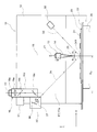
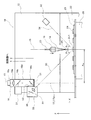
以下本発明の実施形態について図面を参照しながら説明する。図1に示すように、本実施形態のワイヤボンディング装置10は、X軸モータ18とY軸モータ19とによってXY方向に自在に移動するXYテーブル11と、XYテーブル11によってXY方向に自在に移動するボンディングヘッド12と、キャピラリ14が先端に取り付けられた超音波トランスデューサ28と、超音波トランスデューサ28のフランジ部29が固定されるボンディングアーム13と、ボンディングヘッド12に取り付けられ、ボンディングアーム13をZ軸方向に駆動するZ軸モータ20と、ボンディングヘッド12に取り付けられた撮像装置であるカメラ16と、カメラ16に取り付けられた第1の光源31と、半導体チップ23の電極であるパッドを照明する第2の光源32と、半導体チップ23のパッドからの光をカメラ16に導く光学部材33と、半導体チップ23が取り付けられたリードフレーム22を吸着固定するボンディングステージ26と、を備えている。図1において、リードフレーム22の送り方向がX方向、リードフレーム22の表面に沿ってX方向に直角方向がY方向、リードフレーム22の面あるいは半導体チップ23の表面に垂直な上下方向がZ方向で、X方向、Y方向、Z方向は互いに直角である。また、カメラ16は半導体チップ23に向うカメラ光軸17が半導体チップ23に対して垂直となるように取り付けられている。
ボンディングアーム13先端の超音波トランスデューサ28に取り付けられたキャピラリ14は先端が細くなった円錐形であり、その中心にはワイヤ27が挿通される孔が設けられている。ワイヤ27の先端には図示しない電気トーチ等によってイニシャルボール25が形成される。超音波トランスデューサ28に取り付けられたキャピラリ14の先端は、Z軸モータ20とボンディングアーム13によってリードフレーム22またはリードフレーム22に取り付けられた半導体チップ23に対して接離方向に動作する。また、キャピラリ14はボンディングアーム13に固定された超音波トランスデューサ28後端に取りつけられた超音波振動子によってY方向に振動する。キャピラリ中心軸15は、キャピラリ14の先端が半導体チップ23又はリードフレーム22表面に対して垂直に接する様に配置されている。
図2は図1に示したワイヤボンディング装置10の光学系を取り出して模式的に記載したものであり、半導体チップ23に向う鏡筒16dのから撮像素子16aに向うカメラ光軸17とカメラ16の鏡筒16dは直線として記載してある。図2に示すように、カメラ16は鏡筒16dと、鏡筒16dの中に取り付けられたレンズ16eやハーフミラー16b,16cなどによって構成される光学系と光学系によって結像した画像を電気信号に変換するCCD或いはCMOS等の撮像素子16aとを含んでおり、光学系の中心軸であるカメラ光軸17は撮像素子16aの中心を通る線で、取得画像の中心位置を通る線である。カメラ光軸17は撮像する半導体チップ23あるいはリードフレーム22の表面に対して垂直になるように配置されている。カメラ16の鏡筒16dの外側には第1の光源31が取り付けられている。第1の光源は発光ダイオードを用いたものであり、第1の光源31から放射された光は、鏡筒16d内のハーフミラー16bによってその光路が半導体チップ23からカメラ16への撮像光路となるカメラ光軸17と同軸の照明光路17aを通って半導体チップ23の表面を照明するよう構成されている。
図1に示すように、キャピラリ中心軸15とカメラ光軸17とはいずれも半導体チップ23あるいはリードフレーム22の表面に垂直となるように配置されているので、キャピラリ中心軸15とカメラ光軸17とは略平行となっている。そして、図1に示すように、カメラ光軸17は、キャピラリ中心軸15からからX方向オフセット量Xw、Y方向オフセット量Ywだけ離れて配置されている。キャピラリ14はボンディングアーム13を介してボンディングヘッド12に取り付けられており、カメラ16はボンディングヘッド12に固定されているので、キャピラリ中心軸15とカメラ光軸17とは常にX方向オフセット量Xw、Y方向オフセット量Ywを含むオフセット量Wだけ離れてXY方向に同時に移動する。
図1に示すように、第2の光源32は取りつけアームによってボンディングヘッド12に取り付けられている。第2の光源32は第1の光源31と同様、発光ダイオードを用いたものである。図2に示すように、第2の光源32はキャピラリ14の斜め上方で、キャピラリ14に対してX方向にカメラ16と反対側となるように配置されている。また、カメラ16に取り付けられている光学部材33も、キャピラリ14の斜め上方に配置されている。そして、キャピラリ中心軸15がボンディングしようとするパッド241の上に来た際には、第2の光源32からパッド241に向かう光軸34とパッド241から光学部材33に向う光軸34とが同一面内にあってキャピラリ中心軸15に対して対象となるよう配置されている。キャピラリ中心軸15と各光軸34,35との角度はそれぞれθ1となっている。
図2に示すように、光学部材33は、ボンディングしようとするパッド241からの光の方向を変更してカメラ16の鏡筒16dに向わせるミラー36と、焦点の調整を行うレンズ37とが取り付けられている。レンズ37は、パッド241の表面にピントが合うように選択されている。第2の光源32から放射された光は光軸34に沿ってパッド241に進み、パッド241の表面で反射して光軸35に沿って光学部材33のレンズ37に入り、レンズ37を通った後、ミラー36によってカメラ16の鏡筒16dの方向に向かう。そして、カメラ16の鏡筒16dの内部に設けられたハーフミラー16cによって撮像素子16aに向うよう構成されている。
図1に示すように、ワイヤボンディング装置10のXYテーブル11を駆動するX軸モータ18、Y軸モータ19、ボンディングアーム13を駆動するZ軸モータ20、第1の光源31、第2の光源32、カメラ16はそれぞれ制御部60のX軸モータ駆動インターフェース65、Y軸モータ駆動インターフェース66、Z軸モータ駆動インターフェース67、第1の光源駆動インターフェース62、第2の光源駆動インターフェース63、カメラ駆動インターフェース64に接続されている。各インターフェース62~67はデータバス68を介して信号処理を行うCPU61に接続されている。また、制御部60のCPU61には、データバス68を介して動作プログラムやデータを記憶するメモリ70が接続されている。メモリ70には、後で説明するワイヤボンディング装置10のボンディング動作の制御を行うボンディング制御部プログラム71と、その制御用データであるボンディング制御用データ72と、各パッド24の位置を検出するパッド位置検出プログラム73と、カメラ16によって各パッド24の画像を取得するパッド画像取得プログラム74と、イニシャルボールの不着検出を行う不着検出プログラム75と、イニシャルボールの偏芯を検出するボール偏芯検出プログラム76と、第1のシャッタと第2のシャッタの開閉を切り替えるシャッタ切り替えプログラム77とが格納されている。以上説明したように、制御部60は内部に信号処理を行うCPU61とメモリ70とを含むコンピュータである。
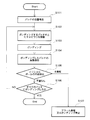
図3から図7A、図7Bを参照しながら、以上のように構成されたワイヤボンディング装置10の動作について説明する。図3のステップS101に示すように、制御部60は図4に示す半導体チップ23の複数のパッド24の位置検出を行うパッド位置検出工程を開始する。図4に示すように、半導体チップ23は、その中央に電子回路が形成されている回路領域23aが配置され、この回路領域23aの外側に回路領域23aと接続されている電極である複数のパッド24が配置されている。回路領域23aは単純なパターンの領域と回路パターンが特徴的な特定領域23d,23eを含んでいる。
図5に示すように、制御部60は、第1の光源31を点灯させ、第2の光源32を消灯させる。第1の光源31から放射された光は、鏡筒16d内のハーフミラー16bによってその光路が半導体チップ23からカメラ光軸17と同軸の照明光路17aを通って半導体チップ23の表面を半導体チップ23の垂直上方から照明する。このとき第2の光源32は消灯されているので、第2の光源32から光学部材33を通ってカメラ16に入る光はなく、カメラ16の撮像素子16aには第1の光源31によって照明される半導体チップ23の表面の画像のみが入力される。
図4に示すように、制御部60は、ボンディングヘッド12をXY方向に移動させ、カメラ光軸17の位置をカメラ16の視野41の中に半導体チップ23の特定領域23dと半導体チップ23の一つの角23bとが含まれる様に位置を調整する。そして、制御部60はメモリに格納している特定領域23dのパターンとカメラ16の撮像素子16aによって取得した画像の中の特定領域23dのパターンとを比較し、視野41の中の特定領域23dの位置から半導体チップ23の特定領域23dの位置を取得する。また、制御部60は取得した画像の特定領域23dと角23bとの距離から半導体チップ23の一つの角23bの位置を取得する。次に、制御部60は先に位置を取得した角23bと対角にある角23cの近傍の特定領域23eと角23cとが視野42に含まれるようにボンディングヘッド12を移動させてカメラ光軸17の位置を調整する。そして、そして、制御部60はメモリに格納している特定領域23eのパターンとカメラ16の撮像素子16aによって取得した画像の中の特定領域23eのパターンとを比較し、視野42の中の特定領域23eの位置から半導体チップ23の特定領域23eの位置を取得し、取得した画像の特定領域23eと角23cとの距離から角23bの対角である角23cの位置を取得する。制御部60は角23bと角23cの位置から半導体チップ23のXY方向の位置、X及びY軸に対する傾きを計算し、メモリに格納している半導体チップ23の各パッド24の配置データに基づいて各パッド24のそれぞれの位置を計算してメモリに格納する(パッド位置検出工程)。
図3のステップS102及び図2に示すように、制御部60は、ボンディングヘッド12によって図3のステップS101で検出した各パッド24の内のボンディングしようとするパッド241の上にキャピラリ14を移動させる。ボンディングしようとするパッド241の上にキャピラリ14が移動すると、図2に示す様に、キャピラリ中心軸15はボンディングしようとするパッド241の略中央に位置し、キャピラリ14はパッド241から少し離れた上方に位置し、キャピラリ14に挿通されたワイヤ27の先端はイニシャルボール25に成形され、キャピラリ14の先端に保持されている。キャピラリ中心軸15がパッド241の上に移動すると、カメラ16はカメラ光軸17がキャピラリ中心軸15とからオフセット量Wだけ離れた位置に移動し、カメラ光軸17は半導体チップ23から外れた位置となっている。なお、図2はXZ面でのワイヤボンディング装置10を示しているので、キャピラリ中心軸15とカメラ光軸17との距離はX方向オフセット量Xwとなっている。
図2に示すように、制御部60は、第1の光源31を消灯し、第2の光源32を点灯する。すると、第1の光源31から放射された光によって照明されていた半導体チップ23の表面が照明されなくなるので、その部分からカメラ光軸17に沿って撮像素子16aに入射する光がなくなる。一方、第2の光源32が点灯されると、第2の光源32から放射された光は、パッド241に向かって光軸34に沿って斜め下に向かって進み、キャピラリ中心軸15と角度θ1を持ってパッド241に当たる。パッド241の表面は鏡面状となっているのでパッド241に当たった光はパッド241の表面で反射し、キャピラリ中心軸15と角度θ1の光軸35に沿って斜め上方に向かって進んで、光学部材33に入る。このように、第1の光源31を消灯し、第2の光源32を点灯することで第2の光源32によって照明されている領域の画像のみをカメラ16の撮像素子16aに入力することができる。
光学部材33に入った光は、レンズ37を通った後、ミラー36によってカメラ16の鏡筒16dに方向を変換される。そして、カメラ16の鏡筒16dに取り付けられたハーフミラー16cによってカメラ光軸17の方向に方向が変換され、カメラ光軸17に沿ってレンズ16eを経て撮像素子16aに入る。
第2の光源32から放射された光は、パッド241の表面だけでなく、その周辺部分にも到達するが、半導体チップ23のパッド241及び各パッド24の周辺部分は、パッド24,241の表面のように鏡面状となってないので、パッド24,241よりも反射する光が少なく、カメラ16の視野では図7A、図7Bに示す様にパッド241の表面が白く映りそれ以外の部分は黒く映る。
キャピラリ14をボンディングしようとするパッド241の上に移動したら、制御部60は図3のステップS103に示すようにボンディングを開始する。制御部60は図2に示した状態から図1に示すZ方向モータを駆動してキャピラリ14を降下させキャピラリ14の先端に保持されているイニシャルボール25をパッド241に向かって押しつける。また、図示しない超音波振動子によってキャピラリ14の先端をY方向に振動させてイニシャルボール25をパッド241に圧着する。この際、半導体チップ23はボンディングステージ26によって所定の温度に加熱されている。
図6に示すように、キャピラリ14によってイニシャルボール25をパッド241の上に押しつけると、イニシャルボール25は押しつけ力によって半球状の圧着ボール25aとなってパッド241に圧着される。そして、制御部60は、図1に示すZ方向モータを駆動してキャピラリ14を上昇させる。ワイヤ27の一端に形成されていたイニシャルボール25は圧着ボール25aとなってパッド241の表面に圧着されているので、キャピラリ14を上昇させると圧着ボール25aからキャピラリ14に向かってワイヤ27が伸びていく。
図3のステップS104に示すように、ボンディングが終わったら、カメラ16の撮像素子16aによってボンディングされたパッド241の画像を取得するパッド画像取得工程を開始する。カメラ16の視野43には図7Aに示すように、ボンディングしたパッド241とすでにボンディングを終了している隣接するパッド240と、次にボンディングするパッド242の3つのパッドの画像が含まれている。先に説明した様に、各パッド240,241,242の各表面は白く映り、半導体チップ23の各パッド240,241,242以外の部分は黒くなる。つまり黒い背景の中に白いパッドか浮き出るような画像となる。また、パッド241にボンディングされている圧着ボール25a及び圧着ボールから伸びるワイヤ27は、第2の光源32から撮像素子16aまでの光路をさえぎるので、視野43の中には黒い影として現れる。このため、視野43では、パッド240,241の圧着ボール25aの位置する部分とワイヤ27の伸びる部分とが白いパッド241の画像の上に黒い画像として現れる(パッド画像取得工程)。
パッドの画像を取得したら、制御部60は、図3のステップS105に示すように、不着検出工程を開始する。制御部60は、取得した図7Aに示すような画像の中から、ボンディングしたパッド241の表面に圧着ボール25a、ワイヤ27と見られる画像があるかどうかを判断する。この判断は、制御部60のメモリに圧着ボール25a、ワイヤ27の基準画像を格納しておき、その基準画像と取得画像を比較してもよいし、各画像を二値化処理し、処理後の画像を比較するようにしてもよいし、パターンマッチングによって比較してもよい。そして、所定の基準を満足する場合には、圧着ボール25a、ワイヤ27がパッド241の上に存在していると判断し、イニシャルボール25はパッド241に圧着され、不着となっていないと判断する(不着検出工程)。
イニシャルボール25が良好にパッド241に圧着されている場合には、図3のステップS106に示すように、制御部60は、半導体チップ23のすべてのパッド24へのボンディングが終了したかを判断する。そして、すべてのパッド24へのボンディングが終了したらボンディングを停止して次の半導体チップ23のパッド24のボンディングに移行する。また。半導体チップ23のすべてのパッド24へのボンディングが終了していない場合には、図3に示すステップS102に戻って、次にボンディングするパッド24の上にキャピラリ14を移動させ、ボンディングとイニシャルボール25の不着検出を続けていく。
一方、イニシャルボール25が良好に圧着されていない場合には、図7Bに示すように、視野44にはパッド241の上には圧着ボール25a、ワイヤ27を示す黒い画像がなくなる。制御部60はこの画像と先に説明した基準画像とを比較して、所定の基準以上の差異がある場合には、イニシャルボール25の不着が発生しているものと判断する。そして、制御部60は図3のステップS107に示すように、不着発生のアラームを発報したり、ワイヤボンディング装置10を停止させたりする。
以上説明した実施形態は、第2の光源32を点灯させて第1の光源を消灯するという機械的な動作を含まない簡便な動作によって、ボンディング中にボンディングしたパッド241の表面の画像を取得し、イニシャルボール25の不着発生の有無を監視することができる。このため、高精度の検出画像によって精度よく不着の発生を監視することができる。また、機械的な可動部分がないのでワイヤボンディング装置が高速となっても精度のよい画像を取得することができると共に、十分な耐久性を備えることができる。さらに、イニシャルボール25の不着が発生した場合に、すぐにアラームを発報したり、ワイヤボンディング装置10を停止させたりして、不良品の発生を抑制することができ、効率的にボンディングを行うことができる。
また、本実施形態では、ボンディングを行う毎にパッド241の画像を取得してイニシャルボール25の不着検出を行うこととして説明したが、カメラ16の視野に複数のパッド24を含めることができる場合には、複数のパッド24へのボンディングか終了した後、複数のパッド24の画像を一括して取得して複数のパッド24へのイニシャルボール25の不着検出を行うようにしてもよい。また、幾つかの検査対象となっているパッド24についてのみイニシャルボール25の不着検出を行うようにしてもよい。
本実施形態ではイニシャルボール25の不着検出を行うこととして説明したが、図3のステップS104で取得した画像からパッド241の外辺と圧着ボール25aの外周との隙間寸法を検出してパッド241の中心に対する圧着ボール25bの偏り量を検出し、圧着ボール25bがパッド241の中心から所定以上偏った位置に有る場合には、ボンディング不良としてイニシャルボール25の不着と同様の処理をすることとしても良い。
図8から図10A,図10Bを参照して図1から図7A,図7Bを参照して説明した実施形態のワイヤボンディング装置10の他の動作について説明する。図1から図7A,図7Bを参照して説明した部分と同様の部分には同様の符号を付して説明は省略する。
図8のステップS201に示すように、制御部60はカメラ16の視野の中に図4に示した半導体チップ23の特定領域23dあるいは23eが含まれる位置にボンディングヘッド12を移動し、先に説明した実施形態の動作と同様に第1の光源31を点灯し、第2の光源32を消灯して半導体チップ23の各パッド24の位置を検出する。そして、図8のステップS202及び図2に示す様に、キャピラリ14をボンディングしようとするパッド241の上に移動する。制御部60は第1の光源31を消灯し、第2の光源32を点灯してボンディングしようとするパッド241を照明する。
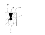
図8のステップS203に示すように、制御部60は、ボンディング動作を開始し、図1に示すZ軸モータ20を駆動して、キャピラリ14の降下を開始する。そして、図9に示すように、キャピラリ14の先端がパッド241の表面の直上まで降下した際に、図8のステップS204に示すように、イニシャルボール25がパッド241に接する直前のイニシャルボール25とキャピラリ14の先端とパッド241との画像を取得する。先に説明したように、キャピラリ14、イニシャルボール25ともに第2の光源32から放射される光をさえぎるので、図10Aに示すようにカメラ16の視野47にはそれぞれ黒い影あるいは画像として現れる。また、イニシャルボール25がパッド241の直上にある状態でキャピラリ14とイニシャルボール25の画像を取得するので、パッド241の表面にピントが合うように選択させている光学部材33の中に入っているレンズ37や、ミラー36の角度を調整することなく精度のよいキャピラリ14、イニシャルボール25の画像を取得することができる。
制御部60は、図8のステップS205に示すように、イニシャルボールの偏芯検出工程を開始する。制御部60は、取得した図10Aに示すような画像の中から、キャピラリ14とキャピラリ14の先端から伸びているイニシャルボール25の画像を認識し、制御部60のメモリに格納されたキャピラリ14からイニシャルボール25が延出したイニシャルボール25の基準画像とを比較し、イニシャルボール25中心とキャピラリ中心軸15との偏芯量を検出する(ボール偏芯検出工程)。
そして、その偏芯量がボンディング不良を発生させないような所定の基準以内であれば、イニシャルボール25の偏芯はないものと判断する。そして、図8のステップS206に示すように、ボンディングを継続し、イニシャルボール25をパッド241にボンディングする。そして、パッド241に圧着ボール25aが形成され、キャピラリ14が上昇したら、図8のステップS207に示すように、ボンディングしたパッド241の画像を取得し、図7A、図7Bに示したようなパッド241と圧着ボール25aとワイヤ27とを含む画像を取得し、図8のステップS208に示すように、イニシャルボール25の不着検出を行う。そして、イニシャルボール25の不着がない場合には、図8のステップS209に示すように、すべてのパッド24にボンディングしたかどうかを判断し、すべてのパッド24にボンディングしていない場合には、図8のステップS203に戻って次にボンディングするパッド24の上にキャピラリ14を移動させる。そして、すべてのパッド24へのボンディングが終了したらワイヤボンディング装置を停止する。
一方、取得した画像が図10Bに示す視野48のような画像で、イニシャルボール25がキャピラリ14のキャピラリ中心軸15から傾いており、キャピラリ中心軸15とイニシャルボール25の中心との間の偏芯量dが所定の基準を超えている場合には、イニシャルボール25の偏芯があるものと判断する。そして、図8のステップS210に示すように、アラームを発報したり、ワイヤボンディング装置10を停止させたりする。また、図8のステップS208でイニシャルボール25の不着が検出された場合も同様にアラームを発報したり、ワイヤボンディング装置10を停止させたりする。
以上説明した実施形態は、先に説明した実施形態と同様の効果に加えて、ボンディングする前にイニシャルボール25の偏芯を検出し、イニシャルボール25の偏芯により発生するボンディング不良を早い段階で検出することができるので、ボンディング不良の発生を抑制することができるという効果を奏する。
図11A、図11Bを参照しながら本発明をバンプボンディング装置に適用した場合について説明する。バンプボンディング装置は先に説明したワイヤボンディング装置と同様の構造で、キャピラリ14によってイニシャルボール25をボンディングしようとするパッド241の表面に圧着した後、ワイヤ27を切断してパッド241の上にバンプ25cを形成するものである。バンプ25cの形状は圧着ボール25aと同様の形状であってもよいし、その目的に応じていろいろな形状とすることができる。
このようにしてイニシャルボール25を圧着させてバンプ25cを形成する際も、圧着ボール25aを形成した場合と同様、第2の光源32を点灯させ、第1の光源を消灯してパッド241周辺の画像を取得すると、図11Aに示す視野45の画像のように、パッド241は白く、バンプ25cとパッド241の周辺の半導体チップ23の表面は黒い画像となる。このように白いパッド241の画像の上に黒いバンプ25cの画像が現れるので、黒いバンプ25cの画像の有無を判断することによってバンプ25cの有無を判断できる。図11Bに示す視野46の画像のように、パッド241の表面にバンプ25c黒い画像がない場合にはイニシャルボール25の不着が発生したと判断する。先に説明した実施形態と同様、イニシャルボール25の不着が発生した場合には、制御部60はアラームを発報したり、バンプボンディング装置を停止されたりする。
本発明をバンプボンディング装置に適用した場合には、本発明をワイヤボンディング装置に適用した場合と同様の効果を奏する。
図12を参照しながら本発明の他の実施形態について説明する。図1から図7A,図7Bを参照して説明した実施形態と同様の部分には同様の符号を付してその説明は省略する。
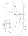
図12に示すように、本実施形態のワイヤボンディング装置10は、カメラ16の鏡筒16dに2つの液晶式の第1、第2のシャッタ51,52を備えている。第1のシャッタ51はカメラ16の先端に設けられており、第2のシャッタ52は、光学部材33とカメラ16との間の光路を遮断する位置に設けられている。第1のシャッタ51は、第1の光源から放射された光の照明光路17aのカメラ16と半導体チップ23との間であって第2の光源32からカメラ光軸17に至る光路を妨げない位置であれば上記以外の位置に配置してもよい。また、第2のシャッタ52は、第2の光源32からの光がパッド241、レンズ37、ミラー36を経て鏡筒16dのハーフミラー16cによってカメラ光軸17の方向に変更される光路の間であって第1の光源31からの照明光路17a、カメラ光軸17に沿った撮像光路を妨げない位置であれば上記以外の位置に配置してもよい。各シャッタ51,52はそれぞれ制御部60に接続され、制御部60によって開閉される。
本実施形態の動作は、図3、図8を参照して説明した実施形態の動作と同様で、制御部60は、図3のステップS101、図8のステップS201に示すように、パッド24の位置を検出する際に第1の光源1を点灯させ第2の光源32を消灯させる場合には、第1のシャッタ51を開として第2のシャッタ52を閉とし、図3のステップS104、図8のステップS207に示すパッド241の画像を取得する際及び図8のステップS204に示すキャピラリ14とイニシャルボール25との画像を取得する際に第2の光源32を点灯させて第1の光源31を消灯する場合には、第2のシャッタを開として第1のシャッタを閉とする(シャッタ切り替え工程)。なお、第1の光源31と第2の光源32は消灯させずに点灯させたままシャッタの切り替えを行ってもよい。
本実施形態は、第1の光源31、第2の光源32を例えばハロゲンランプ等のように点灯、消灯に時間がかかるものを適用した場合、ワイヤボンディング装置10の速度に合わせて第1の光源31からの光と第2の光源からの光とを切り替えることができるという効果を奏する。
図13を参照しながら、他の実施形態のワイヤボンディング装置10について説明する。図1から図12を参照して説明した実施形態と同様の部分には同様の符号を付して説明は省略する。
図13に示すように、本実施形態のワイヤボンディング装置10は、カメラ16の鏡筒16dが直線状に配置され、カメラ16はカメラ光軸17が半導体チップ23に対して垂直となるようにボンディングへッド12に取り付けられている。また、キャピラリ14はボンディングアーム13の先端に取り付けられており、キャピラリ14はボンディングアーム13の後端に取りつけられた超音波振動子によってY方向に振動する。図13に示すように、ワイヤボンディング装置10のXYテーブル11を駆動するX軸モータ18、Y軸モータ19、ボンディングアーム13を駆動するZ軸モータ20、カメラ16、第1の光源31、第2の光源32はそれぞれ制御部60に接続されている。制御部60は、図1に示したように内部に信号処理を行うCPU61と動作プログラムやデータを記憶するメモリ70とを含むコンピュータであり、その内部の構成は図1に記載した構成と同様である。
図13に示したワイヤボンディング装置10は先に図1から図12を参照して説明した実施形態と同様のボンディング動作、パッド位置検出動作、パッド画像取得動作、不着検出動作、ボール偏芯検出動作を行うことができ、先に説明した実施形態と同様、機械的な動作を含まない簡便な動作によって、イニシャルボール25の不着発生の有無を監視することができ、高精度の検出画像によって精度よく不着の発生を監視することができる。また、機械的な可動部分がないのでワイヤボンディング装置が高速となっても精度のよい画像を取得することができると共に、十分な耐久性を備えることができる。さらに、イニシャルボール25の不着が発生した場合に、すぐにアラームを発報したり、ワイヤボンディング装置10を停止させたりして、不良品の発生を抑制することができ、効率的にボンディングを行うことができる。
以上本発明の実施形態につて説明したが、本発明は、ワイヤボンディング装置、バンプボンディング装置のみならず、パッド上にワイヤ等を接続する他のボンディング装置にも適用することができる。
本発明は以上説明した実施形態に限定されるものではなく、請求の範囲により規定されている本発明の技術的範囲ないし本質から逸脱することない全ての変更及び修正を包含するものである。
10 ワイヤボンディング装置、11 XYテーブル、12 ボンディングヘッド、13 ボンディングアーム、14 キャピラリ、15 キャピラリ中心軸、16 カメラ、16a 撮像素子、16b,16c ハーフミラー、16d 鏡筒、16e,37 レンズ、17 カメラ光軸、17a 照明光路、18 X軸モータ、19 Y軸モータ、20 Z軸モータ、22 リードフレーム、23 半導体チップ、23a 回路領域、23b,23c 角、23d,23e 特定領域、24,240,241,242 パッド、25 イニシャルボール、25a 圧着ボール、25c バンプ、26 ボンディングステージ、27 ワイヤ、31 第1の光源、32 第2の光源、33 光学部材、34,35 光軸、36 ミラー、41~48 視野、51 第1のシャッタ、52 第2のシャッタ、60 制御部、61 CPU、62 第1の光源駆動インターフェース、63 第2の光源駆動インターフェース、64 カメラ駆動インターフェース、65 X軸モータ駆動インターフェース、66 Y軸モータ駆動インターフェース、67 Z軸駆動モータインターフェース、68 データバス、70 メモリ、71 ボンディング制御プログラム、72 ボンディング制御データ、73 パッド位置検出プログラム、74 パッド画像取得プログラム、75 不着検出プログラム、76 ボール偏芯検出プログラム、77 シャッタ切り替えプログラム、d 偏芯量、W オフセット量、Xw 方向オフセット量、Yw 方向オフセット量、θ1 角度。
Claims (8)
- ボンディング装置であって、
ボンディングヘッドと、
ボンディングツールと、
撮像装置と、
第1の光源と、
第2の光源と、
光学部材と、
前記第1の光源と前記第2の光源の点灯、消灯を行う制御部とを含み、
前記ボンディングヘッドはXY方向に移動するよう構成され、
前記ボンディングツールは、前記ボンディングヘッドに取り付けられ、Z方向に駆動されて挿通されたワイヤの先端に形成されたイニシャルボールを半導体チップの複数のパッドにそれぞれボンディングするよう構成され、
前記撮像装置は、前記ボンディングツールからX方向及び/又はY方向にオフセットされて前記ボンディングヘッドに取り付けられ、前記半導体チップの画像を撮像するように構成され、
前記第1の光源は、前記撮像装置に取り付けられ、前記半導体チップの特定領域を照明するように構成され、
前記第2の光源は、前記ボンディングツールに対して前記撮像装置と反対側の前記ボンディングヘッドに取り付けられ、その上に前記ボンディングツールが来ている一のパッドを照明するように構成され、
前記光学部材は、前記撮像装置に取り付けられ、前記一のパッドからの光を前記撮像装置に導くように構成され、
前記制御部は、
前記撮像装置の視野に前記半導体チップの前記特定領域が入るように前記ボンディングヘッドをXY方向に移動させ、前記第2の光源を消灯して前記第1の光源を点灯させて前記撮像装置によって前記半導体チップの前記特定領域の画像を取得し、その画像に基づいて前記半導体チップの前記各パッドの位置を検出するパッド位置検出手段と、
前記ボンディングツールが前記各パッドの上に来るように前記ボンディングヘッドをXY方向に移動させ、前記第1の光源を消灯して前記第2の光源を点灯させた状態で前記ボンディングツールによって前記各一のパッドに前記各イニシャルボールを順次ボンディングし、前記撮像装置によってボンディングに応じて前記一のパッドの画像を順次取得するパッド画像取得手段と、
を含んで構成されるボンディング装置。 - 請求項1に記載のボンディング装置であって、
前記撮像装置は、前記半導体チップの表面を垂直上方から撮像するよう配置され、
前記第1の光源から放射された光は、前記半導体チップから前記撮像装置への撮像光路と少なくとも一部が同軸の照明光路を通って前記半導体チップの前記特定領域を照明し、
前記第2の光源と前記光学部材とは、それぞれ前記ボンディングツールの斜め上方に配置され、前記第2の光源から前記一のパッドに向かう光軸と前記一のパッドから前記光学部材に向う光軸とが同一面内にあって前記ボンディングツールのZ方向の移動面に対して対象となるよう配置されているボンディング装置。 - 請求項2に記載のボンディング装置であって、
前記制御部は、
前記ボンディングツールによって前記各パッドに前記各イニシャルボールを順次ボンディングする場合には、取得した各前記一のパッドの各画像に基づいて前記各イニシャルボールの各前記一のパッドへの不着検出を行う不着検出手段、
を有するボンディング装置。 - 請求項3に記載のボンディング装置であって、
前記制御部は、
前記ボンディングツールによって前記各パッドに前記各イニシャルボールを順次ボンディングする場合には、前記各イニシャルボールが前記各一のパッドにボンディングされる直前に、前記第1の光源を消灯し、前記第2の光源を点灯させた状態で前記各一のパッド直上の前記ボンディングツールと前記各イニシャルボールの画像を取得し、その各画像に基づいて前記各イニシャルボールの偏芯を検出するボール偏芯検出手段、
を有するボンディング装置。 - 請求項1に記載のボンディング装置であって、
前記第1の光源から前記半導体チップの前記特定領域を経て前記撮像装置に至る第1の光路と、
前記第2の光源から前記一のパッドを経て前記撮像装置に至る第2の光路と、
前記第1の光路を遮断する第1のシャッタと、
前記第2の光路を遮断する第2のシャッタと、を備え、
前記制御部は、
前記半導体チップの前記特定領域の画像を撮像する場合には、前記第2のシャッタを閉として前記第1のシャッタを開とし、前記一のパッドの画像を撮像する場合には前記第1のシャッタを閉として前記第2のシャッタを開とするシャッタ切り替え手段を備えるボンディング装置。 - 請求項2に記載のボンディング装置であって、
前記第1の光源から前記半導体チップの前記特定領域を経て前記撮像装置に至る第1の光路と、
前記第2の光源から前記一のパッドを経て前記撮像装置に至る第2の光路と、
前記第1の光路を遮断する第1のシャッタと、
前記第2の光路を遮断する第2のシャッタと、を備え、
前記制御部は、
前記半導体チップの前記特定領域の画像を撮像する場合には、前記第2のシャッタを閉として前記第1のシャッタを開とし、前記一のパッドの画像を撮像する場合には前記第1のシャッタを閉として前記第2のシャッタを開とするシャッタ切り替え手段を備えるボンディング装置。 - 半導体チップの複数のパッドへのボンディング方法であって、
XY方向に移動するボンディングヘッドと、前記ボンディングヘッドに取り付けられ、前記各半導体チップの各パッドの上に移動し、挿通されたワイヤの先端に形成されたイニシャルボールを前記半導体チップの前記各パッドにそれぞれボンディングするボンディングツールと、前記ボンディングツールからX方向及び/又はY方向にオフセットされて前記ボンディングヘッドに取り付けられ、前記半導体チップの画像を撮像する共通の撮像装置と、前記撮像装置に取り付けられ、前記半導体チップの特定領域を照明する第1の光源と、前記ボンディングツールに対して前記撮像装置と反対側の前記ボンディングヘッドに取り付けられ、その上に前記ボンディングツールが来ている一のパッドを照明する第2の光源と、前記撮像装置に取り付けられ、前記一のパッドからの光を前記撮像装置に導く光学部材と、を含むボンディング装置を準備する工程と、
前記撮像装置の視野に前記半導体チップの前記特定領域が入るように前記ボンディングヘッドをXY方向に移動させ、前記第2の光源を消灯し、前記第1の光源を点灯させて前記撮像装置によって前記半導体チップの前記特定領域の画像を取得し、その画像に基づいて前記半導体チップの前記各パッドの位置を検出するパッド位置検出工程と、
パッド位置検出工程の後、前記ボンディングツールが前記各パッドの上に来るように前記ボンディングヘッドをXY方向に移動させ、前記第1の光源を消灯し、前記第2の光源を点灯させた状態で前記ボンディングツールによって前記各一のパッドに前記各イニシャルボールを順次ボンディングし、前記撮像装置によってボンディングに応じて前記一のパッドの画像を順次取得するパッド画像取得工程と、
取得した各前記一のパッドの各画像に基づいて前記各イニシャルボールの各前記一のパッドへの不着検出を行う不着検出工程と、
を有するボンディング方法。 - 請求項7に記載のボンディング方法であって、
前記パッド位置検出工程の後、前記ボンディングツールが前記各パッドの上に来るように前記ボンディングヘッドをXY方向に移動させ、前記各イニシャルボールが前記各一のパッドにボンディングされる直前に、前記第1の光源を消灯し、前記第2の光源を点灯させた状態で前記各一のパッド直上の前記ボンディングツールと前記各イニシャルボールの画像を取得し、その各画像に基づいて前記各イニシャルボールの偏芯を検出するボール偏芯検出工程を有するボンディング方法。
Applications Claiming Priority (2)
| Application Number | Priority Date | Filing Date | Title |
|---|---|---|---|
| JP2009-117152 | 2009-05-14 | ||
| JP2009117152A JP4644294B2 (ja) | 2009-05-14 | 2009-05-14 | ボンディング装置及びボンディング方法 |
Publications (1)
| Publication Number | Publication Date |
|---|---|
| WO2010131380A1 true WO2010131380A1 (ja) | 2010-11-18 |
Family
ID=43084767
Family Applications (1)
| Application Number | Title | Priority Date | Filing Date |
|---|---|---|---|
| PCT/JP2009/068669 Ceased WO2010131380A1 (ja) | 2009-05-14 | 2009-10-30 | ボンディング装置及びボンディング方法 |
Country Status (2)
| Country | Link |
|---|---|
| JP (1) | JP4644294B2 (ja) |
| WO (1) | WO2010131380A1 (ja) |
Cited By (3)
| Publication number | Priority date | Publication date | Assignee | Title |
|---|---|---|---|---|
| CN106373914A (zh) * | 2016-11-10 | 2017-02-01 | 北京中电科电子装备有限公司 | 一种芯片键合装置 |
| TWI580511B (zh) * | 2014-06-10 | 2017-05-01 | 新川股份有限公司 | A bonding device, and a method of estimating the placement position of the engagement tool |
| CN115702483A (zh) * | 2020-06-05 | 2023-02-14 | 株式会社新川 | 打线接合装置 |
Families Citing this family (2)
| Publication number | Priority date | Publication date | Assignee | Title |
|---|---|---|---|---|
| MY196886A (en) * | 2016-06-02 | 2023-05-08 | Universal Instruments Corp | Semiconductor die offset compensation variation |
| CN116325102A (zh) * | 2021-01-26 | 2023-06-23 | 株式会社新川 | 打线接合装置、打线接合装置的控制方法以及打线接合装置的控制程序 |
Citations (1)
| Publication number | Priority date | Publication date | Assignee | Title |
|---|---|---|---|---|
| JPH0831899A (ja) * | 1994-07-12 | 1996-02-02 | Toshiba Corp | ボンディングパッドの接合性判定方法 |
Family Cites Families (3)
| Publication number | Priority date | Publication date | Assignee | Title |
|---|---|---|---|---|
| JPH02148746A (ja) * | 1988-11-29 | 1990-06-07 | Nec Corp | ワイヤボンディング装置 |
| JP2973989B2 (ja) * | 1997-11-19 | 1999-11-08 | 日本電気株式会社 | 外観検査機能付きワイヤボンディング装置 |
| EP1174906A1 (de) * | 2000-07-21 | 2002-01-23 | Esec Trading S.A. | Vorrichtung zur Herstellung von Drahtverbindungen |
-
2009
- 2009-05-14 JP JP2009117152A patent/JP4644294B2/ja not_active Expired - Fee Related
- 2009-10-30 WO PCT/JP2009/068669 patent/WO2010131380A1/ja not_active Ceased
Patent Citations (1)
| Publication number | Priority date | Publication date | Assignee | Title |
|---|---|---|---|---|
| JPH0831899A (ja) * | 1994-07-12 | 1996-02-02 | Toshiba Corp | ボンディングパッドの接合性判定方法 |
Cited By (4)
| Publication number | Priority date | Publication date | Assignee | Title |
|---|---|---|---|---|
| TWI580511B (zh) * | 2014-06-10 | 2017-05-01 | 新川股份有限公司 | A bonding device, and a method of estimating the placement position of the engagement tool |
| CN106373914A (zh) * | 2016-11-10 | 2017-02-01 | 北京中电科电子装备有限公司 | 一种芯片键合装置 |
| CN115702483A (zh) * | 2020-06-05 | 2023-02-14 | 株式会社新川 | 打线接合装置 |
| CN115702483B (zh) * | 2020-06-05 | 2026-03-31 | 雅马哈智能机器株式会社 | 打线接合装置 |
Also Published As
| Publication number | Publication date |
|---|---|
| JP2010267756A (ja) | 2010-11-25 |
| JP4644294B2 (ja) | 2011-03-02 |
Similar Documents
| Publication | Publication Date | Title |
|---|---|---|
| JP3802403B2 (ja) | ワイヤボンディング方法及び装置 | |
| TWI655406B (zh) | 接合裝置以及被攝體的高度檢測方法 | |
| JP6240866B2 (ja) | ボンディング装置及びボンディングツールの着地点位置を推定する方法 | |
| CN103196364B (zh) | 元件摄像装置、表面安装机以及元件检查装置 | |
| KR101962888B1 (ko) | 와이어 본딩 장치 및 와이어 본딩 방법 | |
| JP5660810B2 (ja) | 部品実装機の吸着ノズル検査装置 | |
| TWI894380B (zh) | 疊合焊線之迴路高度測量裝置及方法 | |
| JP4644294B2 (ja) | ボンディング装置及びボンディング方法 | |
| CN101320703A (zh) | 焊接装置用摄像装置及摄像方法 | |
| CN111279462B (zh) | 接合装置 | |
| JP2008306040A (ja) | ボンディング装置用撮像装置及び撮像方法 | |
| TW200408018A (en) | Bonding apparatus | |
| JP6047723B2 (ja) | ダイボンダおよびボンディングツールと半導体ダイとの相対位置の検出方法 | |
| JP2014036068A (ja) | ダイボンダおよびボンディングツールの位置検出方法 | |
| JP6182248B2 (ja) | ダイボンダ | |
| KR101124566B1 (ko) | 웨이퍼 검사장치 | |
| US20250216341A1 (en) | Inspection apparatus and inspection method | |
| JP2010278128A (ja) | ボンディング装置及びボンディング装置のオフセット量補正方法 | |
| KR20250134528A (ko) | 반도체 디바이스 핸들링 장치 및 반도체 디바이스 시험 장치 | |
| CN115376960A (zh) | 一种识取组件、定位组件、固晶机及固晶方法 | |
| JP2001280928A (ja) | 形状認識方法および形状認識装置 | |
| KR20060117796A (ko) | 표면실장부품의 흡착 확인 장치 |
Legal Events
| Date | Code | Title | Description |
|---|---|---|---|
| 121 | Ep: the epo has been informed by wipo that ep was designated in this application |
Ref document number: 09844650 Country of ref document: EP Kind code of ref document: A1 |
|
| NENP | Non-entry into the national phase |
Ref country code: DE |
|
| 122 | Ep: pct application non-entry in european phase |
Ref document number: 09844650 Country of ref document: EP Kind code of ref document: A1 |