WO2010128809A2 - 니켈-인-텅스텐 삼원합금 무전해 도금액, 이를 이용한 무전해 도금 공정 및 이에 의해 제조된 니켈-인-텅스텐 삼원합금피막 - Google Patents
니켈-인-텅스텐 삼원합금 무전해 도금액, 이를 이용한 무전해 도금 공정 및 이에 의해 제조된 니켈-인-텅스텐 삼원합금피막 Download PDFInfo
- Publication number
- WO2010128809A2 WO2010128809A2 PCT/KR2010/002882 KR2010002882W WO2010128809A2 WO 2010128809 A2 WO2010128809 A2 WO 2010128809A2 KR 2010002882 W KR2010002882 W KR 2010002882W WO 2010128809 A2 WO2010128809 A2 WO 2010128809A2
- Authority
- WO
- WIPO (PCT)
- Prior art keywords
- phosphorus
- nickel
- tungsten
- electroless plating
- plating solution
- Prior art date
- Legal status (The legal status is an assumption and is not a legal conclusion. Google has not performed a legal analysis and makes no representation as to the accuracy of the status listed.)
- Ceased
Links
Images

Classifications
-
- C—CHEMISTRY; METALLURGY
- C23—COATING METALLIC MATERIAL; COATING MATERIAL WITH METALLIC MATERIAL; CHEMICAL SURFACE TREATMENT; DIFFUSION TREATMENT OF METALLIC MATERIAL; COATING BY VACUUM EVAPORATION, BY SPUTTERING, BY ION IMPLANTATION OR BY CHEMICAL VAPOUR DEPOSITION, IN GENERAL; INHIBITING CORROSION OF METALLIC MATERIAL OR INCRUSTATION IN GENERAL
- C23C—COATING METALLIC MATERIAL; COATING MATERIAL WITH METALLIC MATERIAL; SURFACE TREATMENT OF METALLIC MATERIAL BY DIFFUSION INTO THE SURFACE, BY CHEMICAL CONVERSION OR SUBSTITUTION; COATING BY VACUUM EVAPORATION, BY SPUTTERING, BY ION IMPLANTATION OR BY CHEMICAL VAPOUR DEPOSITION, IN GENERAL
- C23C18/00—Chemical coating by decomposition of either liquid compounds or solutions of the coating forming compounds, without leaving reaction products of surface material in the coating; Contact plating
- C23C18/16—Chemical coating by decomposition of either liquid compounds or solutions of the coating forming compounds, without leaving reaction products of surface material in the coating; Contact plating by reduction or substitution, e.g. electroless plating
- C23C18/31—Coating with metals
- C23C18/32—Coating with nickel, cobalt or mixtures thereof with phosphorus or boron
- C23C18/34—Coating with nickel, cobalt or mixtures thereof with phosphorus or boron using reducing agents
-
- C—CHEMISTRY; METALLURGY
- C23—COATING METALLIC MATERIAL; COATING MATERIAL WITH METALLIC MATERIAL; CHEMICAL SURFACE TREATMENT; DIFFUSION TREATMENT OF METALLIC MATERIAL; COATING BY VACUUM EVAPORATION, BY SPUTTERING, BY ION IMPLANTATION OR BY CHEMICAL VAPOUR DEPOSITION, IN GENERAL; INHIBITING CORROSION OF METALLIC MATERIAL OR INCRUSTATION IN GENERAL
- C23C—COATING METALLIC MATERIAL; COATING MATERIAL WITH METALLIC MATERIAL; SURFACE TREATMENT OF METALLIC MATERIAL BY DIFFUSION INTO THE SURFACE, BY CHEMICAL CONVERSION OR SUBSTITUTION; COATING BY VACUUM EVAPORATION, BY SPUTTERING, BY ION IMPLANTATION OR BY CHEMICAL VAPOUR DEPOSITION, IN GENERAL
- C23C18/00—Chemical coating by decomposition of either liquid compounds or solutions of the coating forming compounds, without leaving reaction products of surface material in the coating; Contact plating
- C23C18/16—Chemical coating by decomposition of either liquid compounds or solutions of the coating forming compounds, without leaving reaction products of surface material in the coating; Contact plating by reduction or substitution, e.g. electroless plating
- C23C18/48—Coating with alloys
- C23C18/50—Coating with alloys with alloys based on iron, cobalt or nickel
-
- H—ELECTRICITY
- H10—SEMICONDUCTOR DEVICES; ELECTRIC SOLID-STATE DEVICES NOT OTHERWISE PROVIDED FOR
- H10P—GENERIC PROCESSES OR APPARATUS FOR THE MANUFACTURE OR TREATMENT OF DEVICES COVERED BY CLASS H10
- H10P14/00—Formation of materials, e.g. in the shape of layers or pillars
- H10P14/40—Formation of materials, e.g. in the shape of layers or pillars of conductive or resistive materials
- H10P14/46—Formation of materials, e.g. in the shape of layers or pillars of conductive or resistive materials using a liquid
-
- H—ELECTRICITY
- H10—SEMICONDUCTOR DEVICES; ELECTRIC SOLID-STATE DEVICES NOT OTHERWISE PROVIDED FOR
- H10W—GENERIC PACKAGES, INTERCONNECTIONS, CONNECTORS OR OTHER CONSTRUCTIONAL DETAILS OF DEVICES COVERED BY CLASS H10
- H10W20/00—Interconnections in chips, wafers or substrates
- H10W20/01—Manufacture or treatment
- H10W20/031—Manufacture or treatment of conductive parts of the interconnections
- H10W20/032—Manufacture or treatment of conductive parts of the interconnections of conductive barrier, adhesion or liner layers
- H10W20/033—Manufacture or treatment of conductive parts of the interconnections of conductive barrier, adhesion or liner layers in openings in dielectrics
- H10W20/037—Manufacture or treatment of conductive parts of the interconnections of conductive barrier, adhesion or liner layers in openings in dielectrics the barrier, adhesion or liner layers being on top of a main fill metal
Definitions
- the present invention relates to a nickel-phosphorus tungsten tert-alloy electroless plating solution, an electroless plating process using the same, and a nickel-phosphorus-tungsten tert-alloy coating prepared thereby, and more particularly, to plating by using tungsten, a high melting point metal.
- the present invention relates to a nickel-phosphorus-tungsten tertiary alloy electroless plating solution which prevents diffusion of copper inside a film and improves thermal stability, an electroless plating process using the same, and a nickel-phosphorus-tungsten tertiary alloy film prepared thereby.
- the signal transfer speed of the semiconductor chip is generally lowered by the resistance-capacitance delay (RC delay) occurring in the metal wiring. That is, the RC delay caused by the resistance of the wiring and the capacitance of the interlayer insulating film negatively affects the speed of the device to be improved.
- RC delay resistance-capacitance delay
- copper does not have a large passivation effect due to its own surface oxide film, so that the surface is easily oxidized, and it is easy to form silicide due to its strong reactivity with silicon.
- the diffusion coefficient of copper in silicon or silicon dioxide is about 100 times larger than that of ordinary metals, a reliable diffusion barrier layer is required to prevent destruction of the semiconductor device by heat treatment.
- metal has a characteristic of having a diffusion coefficient at a surface or an interface rather than a bulk. In a semiconductor, diffusion occurs well at an interface between a metal wiring layer and a diffusion barrier layer. In addition, contrary to the expectation that copper has a 1.64 times higher melting point than aluminum, the resistance to EM (Electromigration) is not significantly different in actual wiring, and the interface where the main diffusion path of wiring material exists between dissimilar materials It can be seen that.
- EM Electromigration
- electroless plating refers to plating by chemical reaction without using electricity, in which metal ions contained in a plating solution are plated using the principle that electrons are received and reduced and adhere to the surface of an object to be plated. .
- a diffusion barrier layer having high thermal stability at high temperature is required.
- An object of the present invention is to improve the diffusion prevention effect and thermal stability of copper than the diffusion barrier layer formed by the conventional electroless plating solution, to ensure the reliability of microcircuits in various semiconductors and packages and printed circuit boards requiring copper wiring It is to provide a nickel-phosphorus-tungsten tertiary alloy electroless plating solution.
- the present invention provides a nickel-phosphorus-tungsten terpolymer comprising nickel sulfate as a metal salt, sodium hypophosphite as a reducing agent, sodium tungstate as a tungsten alloy source, succinic acid, lactic acid and citric acid as a complexing agent.
- a nickel-phosphorus-tungsten terpolymer comprising nickel sulfate as a metal salt, sodium hypophosphite as a reducing agent, sodium tungstate as a tungsten alloy source, succinic acid, lactic acid and citric acid as a complexing agent.
- the nickel-phosphorus-tungsten three-alloy electroless plating solution may have a composition shown in Table 1 below.
- Nickel sulfate used as the metal salt is preferably used 20 ⁇ 30g / L. If the concentration of nickel sulfate is less than 20g / L, the plating rate is lowered, and if the concentration of nickel sulfate is more than 30g / L, the plating rate is increased, but there is a disadvantage that decomposition of the plating liquid easily occurs.
- the reducing agent is for reducing nickel ions, and sodium hypophosphite used as the reducing agent is preferably used in a range of 50 to 100 g / L. If the concentration of sodium hypophosphite is less than 50 g / L plating rate is lowered, productivity is lowered, if the concentration exceeds 100 g / L, the plating rate is increased, but the stability of the solution is lowered, there is a disadvantage that the decomposition of the plating solution.
- sodium tungstate As the tungsten alloy source, sodium tungstate, tungsten oxide, tungsten chloride, carbonyl tungsten chloride, and the like may be used, and preferably sodium tungstate. In this invention, it is preferable to use 10-20 g / L sodium tungstate. If the concentration of sodium tungstate is less than 10 g / L, the plating film is less than the content, it is difficult to achieve the desired function, if it exceeds 20 g / L there is a problem that the plating adhesion is significantly weakened.
- the plating solution according to the present invention may include nickel 4.5 to 6.7 g / L, phosphorus 14.6 to 29 g / L, tungsten 6.3 to 12.5 g / L.
- the complexing agent is to control the plating rate and prevent the spontaneous decomposition of the plating to provide a composition with excellent solution stability, according to one embodiment of the present invention, succinic acid 5 ⁇ 20g / L, lactic acid 5 ⁇ 20g / L And citric acid 5-10 g / L. If the concentration of the complexing agent is too small, the amount of nickel ions which are not complexed increases, so that the plating is not effective. If the concentration is too high, the plating solution stability is increased but the plating speed is lowered.
- the nickel-phosphorus-tungsten tertiary alloy electroless plating solution of the present invention may include additives such as brighteners and stabilizers, pH adjusters, and the like, as necessary.
- the additives such as the brightening agent and the stabilizer are to prevent the natural decomposition of the plating solution and the gloss of the plating film.
- a lead compound as a brightening agent, a thallium compound as a stabilizer, and the additive is used at a concentration of 1 to 5 ppm. It is desirable to.
- the pH adjuster to adjust the pH of the plating solution, in the present invention is maintained at pH 7 to 8 using ammonia water or sulfuric acid. In this pH range, the plating speed is fast and the plating is effectively performed, and there is an advantage of suppressing chemical erosion and / or corrosion of the device.
- an electroless plating process comprising forming a diffusion barrier layer on a copper surface by plating copper using a nickel-phosphorus-tungsten electroless ternary alloy plating solution according to the present invention.
- the electroless plating process is preferably carried out in a temperature range of 50 ⁇ 70 °C and 7.0 ⁇ 8.0 pH range. These process conditions are set to minimize mechanical or chemical effects on the device on which the diffusion barrier layer is formed. According to this process temperature, deformation and erosion of materials are minimized, and a dense and fine alloy coating structure can be formed. In addition, according to such PH working conditions, chemical erosion or corrosion of the device can be suppressed.
- a nickel-phosphorus-tungsten tertiary alloy film plated on a copper surface by a nickel-phosphorus-tungsten electroless ternary alloy plating solution according to the present invention is provided.
- the thickness of the nickel-phosphorus-tungsten tertiary alloy film is 30 ⁇ 100nm
- the vacancy amount of tungsten may be 1 to 5% by weight
- the vacancy amount of phosphorus may be 5 to 8% by weight.
- the electroless plating process according to the present invention can be performed in a low temperature and neutral pH range, thereby reducing chemical erosion or deformation in other materials when forming a selective coating.
- the nickel-phosphorus-tungsten tertiary alloy electroless plating solution according to the present invention prevents diffusion of copper in the plating film and improves thermal stability by using tungsten, which is a high melting point metal, thereby improving various semiconductors, packages, and printed circuit boards. It can be usefully used in.
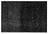
- Figure 2 is a SEM photograph of the nickel-phosphorus-tungsten tertiary alloy film according to an embodiment of the present invention
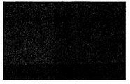
- FIG. 3 is a SEM photograph showing the cross-sectional structure of the nickel-phosphorus-tungsten three-way alloy film according to an embodiment of the present invention
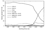
- FIG. 4 is a graph of an interlayer analysis of a nickel-phosphorus-tungsten tert-alloy film formed by a nickel-phosphorus-tungsten tert-alloy electroless plating solution according to an embodiment of the present invention at room temperature using a photoelectron spectrometer (XPS).
- XPS photoelectron spectrometer
- FIG. 5 is an interlayer analysis using a photoelectron spectroscopy (XPS) after a nickel-phosphorus-tungsten tert-alloy film formed by a nickel-phosphorus-tungsten tert-alloy electroless plating solution according to an embodiment of the present invention after heat treatment at 500 ° C. It is a graph.
- XPS photoelectron spectroscopy
- Titanium and copper having a thickness of 20 nm were formed on a wafer material having a thickness of 100 to 150 nm.
- the pickling process was performed at 25 to 30 ° C. for 1 to 2 minutes to remove the oxide of copper, followed by washing with non-ionized water.
- soft etching and water washing were performed at room temperature for 1 to 2 minutes, and the surface was activated with a palladium metal catalyst, and then nickel-phosphorus was used as a diffusion barrier layer using a nickel-phosphorus-tungsten tertiary alloy electroless plating solution.
- a tungsten ternary alloy film was formed.
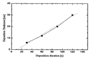
- the formation rate of the plated film with time is shown in FIG. 1, and referring to FIG. 1, the plated film formation rate is 3.8 ⁇ m / hr, and it can be seen that it exhibits easy characteristics for forming a thin film.
- the formed nickel-phosphorus-tungsten tertiary alloy film was observed with a scanning electron microscope (SEM) and the photograph is shown in FIG.
- the cross-sectional structure of the nickel-phosphorus tungsten terpolymer coating was observed by scanning electron microscopy (SEM), and the photograph is shown in FIG. 3, and it was confirmed that a nickel-phosphorus-tungsten tert alloy coating having a thickness of about 50 nm was formed.
- XPS X-ray Photoelectron Spectroscopy
Landscapes
- Chemical & Material Sciences (AREA)
- General Chemical & Material Sciences (AREA)
- Chemical Kinetics & Catalysis (AREA)
- Engineering & Computer Science (AREA)
- Materials Engineering (AREA)
- Mechanical Engineering (AREA)
- Metallurgy (AREA)
- Organic Chemistry (AREA)
- Chemically Coating (AREA)
Abstract
본 발명은 니켈-인-텅스텐 삼원합금 무전해 도금액, 이를 이용한 무전해 도금 공정 및 이에 의해 제조된 니켈-인-텅스텐 삼원합금피막에 관한 것으로, 본 발명에 따른 무전해 도금 공정은 낮은 온도와 중성 pH 영역에서 수행됨에 따라 선택적인 도금피막 형성시 다른 소재에 화학적인 침식 또는 변형을 감소시킬 수 있으며, 본 발명에 따른 니켈-인-텅스텐 삼원합금 무전해 도금액은 고융점 금속인 텅스텐을 사용함으로써 도금피막 내부의 구리의 확산을 방지하고, 열적안정성이 향상되므로, 각종 반도체 및 패키지와 인쇄회로기판에서 유용하게 사용될 수 있다.
Description
본 발명은 니켈-인-텅스텐 삼원합금 무전해 도금액, 이를 이용한 무전해 도금 공정 및 이에 의해 제조된 니켈-인-텅스텐 삼원합금피막에 관한 것으로, 보다 상세하게는 고융점 금속인 텅스텐을 사용함으로써 도금피막 내부의 구리의 확산을 방지하고, 열적안정성이 향상되는 니켈-인-텅스텐 삼원합금 무전해 도금액, 이를 이용한 무전해 도금 공정 및 이에 의해 제조된 니켈-인-텅스텐 삼원합금피막에 관한 것이다.
반도체 칩의 신호 전달속도는 일반적으로 금속 배선에서 발생하는 저항-축전용량 지연(RC delay)에 의하여 저하된다. 즉, 배선의 저항과 층간 절연막의 축전용량에 의해 야기되는 RC 지연은 향상시키려는 소자의 속도에 부정적인 영향을 미친다. 종래에는 배선 재료로써 알루미늄(Al)을 많이 사용하였으나, 알루미늄보다는 구리(Cu)가 전기이동도(electromigration)에 대한 저항이 커서 반도체 소자의 신뢰성을 향상시킬 수 있고, 비저항이 알루미늄의 1/2 수준이어서 작은 폭으로 형성하여도 신호전달 속도를 증가시킬 수 있기 때문에, 집적 회로에 유용한 배선 재료로 떠오르고 있다. 뿐만 아니라, 구리는 소비전력이 작고 알루미늄에 비하여 저렴하다. 그런데 구리는 식각하기 어려운 물질이라서, 증착한 다음에 원하는 배선 모양으로 패터닝하기가 어렵다. 따라서, 최근에는 층간 절연막으로 배선 모양의 홈을 미리 형성한 다음에 구리로 채우는 다마신(damascene) 구리 배선공정이 이용되고 있다. 특히 비아 트렌치와 그 상부에 중첩되는 배선 트렌치를 형성한 다음, 한번의 구리 증착으로 두 트렌치를 모두 채우는 듀얼 다마신법이 널리 이용되고 있다. 트렌치 내에 구리를 채우는 데에는 스퍼터링이나 CVD가 흔히 사용되는데, 이러한 방법은 비용이 많이 들고, 구리 원료로부터 구리를 얻어내는 데에 많은 에너지가 소요되며 복잡하다는 문제가 있다.
또한, 구리는 기존 배선재료로 사용되던 알루미늄과 달리, 자체 표면 산화막에 의한 보호(passivation) 효과가 크지 않아 표면이 산화되기가 용이하고, 실리콘과의 반응성이 강하여 실리사이드(silicide)를 형성하기 쉽다. 또한, 실리콘 또는 이산화규소 내에서의 구리의 확산계수가 보통의 금속에 비하여 약 100 배 정도가 크므로, 열처리에 의한 반도체 소자의 파괴를 막기 위해서는 신뢰성 있는 확산 방지층이 필요하다.
일반적으로 금속은 내부(bulk) 보다 표면 또는 계면(interface)에서의 확산계수가 큰 특성을 나타내는데, 반도체에서도 금속배선층과 확산방지층간의 계면에서 확산이 잘 일어난다. 또한, 구리가 알루미늄 보다 1.64배 융점이 높아 EM(Electromigration)에 대한 저항성이 클 것이라는 예상과는 달리, 실제 배선에서는 큰 차이를 보이지 않고 있어, 배선재료의 주된 확산경로가 이종재료 사이에 존재하는 계면이라는 것을 알 수 있다.
따라서, 배선재료의 EM에 인한 신뢰성 문제를 해결하면서 다마신 구리 배선공정을 최대한 적용하기 위해서는 확산방지층의 대체 재료 및 대체 재료를 사용하여 확산방지층을 용이하게 형성할 수 있는 방법에 대한 연구가 요구된다. 종래에는 기존의 프라즈마 코팅장치를 이용하여 SiN 혹은 SiCN과 같은 하드마스크(hardmask) 타입의 확산방지 피복층(Capping Layer)을 형성하였으나, 유전율(dielectric constant)이 다소 높아 배선 캐퍼시턴스(wiring capacitance)가 증가한다는 문제점이 있었다.
이를 해결하기 위해, SiN 혹은 SiCN과 같은 하드마스크 타입의 확산방지층보다 낮은 전기적 저항으로 배선의 캐퍼시턴스(wiring capacitance)를 낮출 수 있으면서도, EM 혹은 SM(stressmigration)으로 인한 배선재료의 힐락의 발생을 기계적으로 최대한 억제할 수 있는 기술로서, 무전해 도금으로 형성된 확산방지층이 연구되고 있다. 여기서 무전해 도금(electroless plating)이란, 전기를 사용하지 않고 화학 반응을 통해 도금하는 방식으로, 도금액에 포함된 금속이온이 전자를 받아서 환원되어 도금되는 물체의 표면에 달라붙는 원리를 이용하여 도금된다.
그러나, 높은 온도의 후속 공정에 의한 구리 배선의 산화에 의한 저항상승을 방지하고, 계면에서의 구리의 확산에 의한 EM을 억제하기 위해서는 높은 온도에서 열적 안정성이 높은 확산방지층이 요구되고 있다.
본 발명의 목적은 종래의 무전해 도금 용액에 의해 형성되는 확산방지층보다 구리의 확산 방지 효과와 열적 안정성을 향상시켜, 구리배선이 필요한 각종 반도체 및 패키지와 인쇄회로기판에서의 미세회로의 신뢰성을 확보할 수 있는 니켈-인-텅스텐 삼원합금 무전해 도금액을 제공하는 것이다.
본 발명의 다른 목적은 낮은 온도와 중성 pH 영역에서 수행됨으로써 선택적인 도금피막 형성시 다른 소재에 화학적 침식 또는 변형을 감소시킬 수 있는 무전해 도금 공정을 제공하는 것이다.
본 발명의 또 다른 목적은 확산 방지 효과가 향상된 니켈-인-텅스텐 무전해 삼원합금 도금액에 의해 구리 표면 상에 도금된 니켈-인-텅스텐 삼원합금피막을 제공하는 것이다.
상기 목적을 달성하기 위하여 하나의 양상으로서, 본 발명은 금속염으로서 황산니켈, 환원제로서 차아인산 나트륨, 텅스텐 합금원으로서 텅스텐산 나트륨, 착화제로 숙신산, 락트산 및 시트린산을 포함하는 니켈-인-텅스텐 삼원합금 무전해 도금액을 제공한다.
본 발명의 일구현예에 따르면, 상기 니켈-인-텅스텐 삼원합금 무전해 도금액은 하기 표 1에 나타낸 조성을 가질 수 있다.
표 1
| 도금액 | ||
| 금속염 | 황산니켈 (NiSO4) | 20~30g/ℓ(니켈: 4.5~6.7g/L) |
| 텅스텐산 나트륨 (Na2WO2) | 10~20g/ℓ(텅스텐:6.3~12.5g/L) | |
| 차아인산나트륨 (NaH2PO2) | 50~100g/ℓ(인:14.6~29g/L) | |
| 환원제 | 숙신산 (Succinate) | 5~20g/ℓ |
| 착화제 | 락트산 (Lactic) | 5~20g/ℓ |
| 시트린산 (Citrate) | 5~10g/ℓ | |
| 온도 | 50~70℃ | |
| pH | 7~8 | |
상기 금속염으로 사용되는 황산니켈은 20~30g/L 사용하는 것이 바람직하다. 황산니켈의 농도가 20g/L 미만이면 도금속도가 저하되고, 30g/L를 초과하는 경우는 도금속도는 증가하지만 도금액의 분해가 일어나기 쉬운 단점이 있다.
상기 환원제는 니켈 이온을 환원시키기 위한 것으로, 환원제로서 사용되는 차아인산 나트륨은 50~100g/L 사용하는 것이 바람직하다. 차아인산 나트륨의 농도가 50g/L 미만이면 도금속도가 저하되어 생산성이 저하되며, 100g/L를 초과하는 경우는 도금속도는 증가하지만 용액의 안정성이 저하되어 도금액의 분해가 일어나기 쉬운 단점이 있다.
상기 텅스텐 합금원으로는 텅스텐산 나트륨, 텅스텐 옥사이드, 염화텅스텐, 염화카보닐텅스텐 등을 사용할 수 있으며, 바람직하게는 텅스텐산 나트륨을 사용할 수 있다. 본 발명에서는 텅스텐산 나트륨 10~20g/L 사용하는 것이 바람직하다. 텅스텐산 나트륨의 농도가 10g/L 미만이면 도금막이 함량 미달로 목적한 기능을 달성하기 어렵고, 20g/L를 초과하는 경우는 도금밀착력이 현저하게 약해지는 문제가 있다.
더욱 구체적으로는, 본 발명에 따른 도금액은 니켈 4.5~6.7g/L, 인 14.6~29g/L, 텅스텐 6.3~12.5g/L을 포함할 수 있다.
한편, 착화제는 도금속도를 조절하며 도금이 자발적으로 분해되는 것을 방지하여 용액 안정성이 우수한 조성을 제공하는 것으로, 본 발명의 일구현예에 따르면, 숙신산 5~20g/L, 락트산 5~20g/L 및 시트린산 5~10g/L을 사용하는 것이 바람직하다. 만일 착화제의 농도가 너무 적을 경우 착화되지 않는 니켈 이온의 양이 많아져 도금이 효과적으로 되지 않고, 농도가 너무 많을 경우 도금액의 안정성은 증가하나 도금속도가 저하된다.
본 발명의 니켈-인-텅스텐 삼원합금 무전해 도금액은 필요에 따라 광택제 및 안정화제와 같은 첨가제, pH 조절제 등을 포함할 수 있다.
상기 광택제 및 안정화제와 같은 첨가제는 도금액의 자연분해를 방지하고 도금 피막의 광택을 위한 것으로, 본 발명에서는 광택제로 납 화합물, 안정화제로 탈륨 화합물을 포함하며, 첨가제는 1~5 ppm의 농도로 사용하는 것이 바람직하다.
상기 pH 조절제는 도금액의 pH를 조절하는 것으로, 본 발명에서는 암모니아수 또는 황산을 사용하여 pH 7 내지 8로 유지시킨다. 이러한 pH 범위에서는 도금의 속도가 빠르면서 도금이 효과적으로 잘 이루어질 뿐 아니라, 소자의 화학적 침식 및/또는 부식을 억제할 수 있는 이점이 있다.
본 발명의 다른 양상에 따르면, 본 발명에 따른 니켈-인-텅스텐 무전해 삼원합금 도금액을 사용하여 구리를 도금하여 구리 표면 상에 확산방지층을 형성하는 단계를 포함하는 무전해 도금 공정을 제공한다.
이때, 상기 무전해 도금 공정은 50~70℃의 온도 범위 및 7.0~8.0 pH 범위에서 수행되는 것이 바람직하다. 이러한 공정 조건은 확산방지층이 형성되는 소자에 기계적 또는 화학적 영향을 최소화하도록 설정된 것이다. 이러한 공정온도에 의하면, 재료의 변형이나 침식 등이 최소화되며 치밀하고 미세한 합금 피막조직이 형성될 수 있다. 또한 이러한 PH 작업조건에 의하면, 소자의 화학적 침식 또는 부식이 억제될 수 있다.
본 발명의 다른 양상에 따르면, 본 발명에 따른 니켈-인-텅스텐 무전해 삼원합금 도금액에 의해 구리 표면 상에 도금된 니켈-인-텅스텐 삼원합금피막을 제공한다.
이때, 상기 니켈-인-텅스텐 삼원합금피막의 두께는 30~100nm이고, 텅스텐의 공석량은 1~5중량%, 인의 공석량은 5~8중량%일 수 있다. 상기와 같은 니켈-인-텅스텐 무전해 삼원합금 도금액에 의해 피막을 형성하면, 안정된 도금액 상태에서 치밀한 미세 조직을 형성하고, 열적 안정성 및 화학적 기계적 물성을 향상시킬 수 있다. 더욱이, 적절한 착화제의 사용과 합금원소로 첨가되는 텅스텐에 의해 상승하는 내부응력으로 인한 균열 발생이 억제될 수 있다.
본 발명에 따른 무전해 도금 공정은 낮은 온도와 중성 pH 영역에서 수행됨으로써 선택적인 도금피막 형성시 다른 소재에 화학적 침식 또는 변형을 감소시킬 수 있다. 또한, 본 발명에 따른 니켈-인-텅스텐 삼원합금 무전해 도금액은 고융점 금속인 텅스텐을 사용함으로써 도금피막 내부의 구리의 확산을 방지하고, 열적안정성이 향상되므로, 각종 반도체 및 패키지와 인쇄회로기판에서 유용하게 사용될 수 있다.
도 1은 본 발명의 일구현예에 따른 니켈-인-텅스텐 삼원합금피막의 시간에 따른 생성속도를 나타내는 그래프이며,
도 2는 본 발명의 일구현예에 따른 니켈-인-텅스텐 삼원합금피막의 SEM 사진이며,
도 3은 본 발명의 일구현예에 따른 니켈-인-텅스텐 삼원합금피막의 단면조직을 도시하는 SEM 사진이며,
도 4는 본 발명의 일구현예에 따른 니켈-인-텅스텐 삼원합금 무전해 도금액에 의해 형성된 니켈-인-텅스텐 삼원합금피막을 상온에서 광전자분광기(XPS)를 이용하여 층간 분석한 그래프이며,
도 5는 본 발명의 일구현예에 따른 니켈-인-텅스텐 삼원합금 무전해 도금액에 의해 형성된 니켈-인-텅스텐 삼원합금피막을 500℃에서 열처리 한 후의 광전자분광기(XPS)를 이용하여 층간 분석한 그래프이다.
이하, 실시예는 본 발명의 권리범위를 한정하는 것이 아니라 본 발명의 청구범위에 제시된 구성요소의 예시적인 사항에 불과하며, 본 발명의 명세서 전반에 걸친 기술사상에 포함되고 청구범위의 구성요소에서 균등물로서 치환 가능한 구성요소를 포함하는 실시예는 본 발명의 권리범위에 포함될 수 있다.
<실시예>
20nm의 두께의 티타늄과 구리를 100~150nm의 두께로 형성된 웨이퍼 소재에, 먼저 구리의 산화막을 제거하기 위해 25~30℃에서 1~2분간 산세 처리한 후 비이온수로 세척하였다. 밀착력 향상을 위해서 상온에서 1~2분간 소프트 에칭처리와 수세를 실시하고, 파라듐 금속촉매로 표면을 활성화시킨 후, 니켈-인-텅스텐 삼원합금 무전해 도금액을 이용하여 확산방지층으로서 니켈-인-텅스텐 삼원합금피막을 형성하였다. 시간에 따른 도금피막의 생성속도를 도 1에 나타내었으며, 도 1을 참조하면, 도금피막 형성속도는 3.8㎛/hr로, 박막형성에 용이한 특성을 나타내는 것을 알 수 있다.
한편, 이러한 작업을 통해 얻어진 시편의 피막에 공석된 합금의 공석량 및 도금속도를 관찰하여 표 2에 나타내었다. 확산방지층에 공석된 인 함량은 6.75중량%, 텅스텐은 1.3중량%를 나타냄을 확인할 수 있으며, 니켈은 양은 rest 또는 그 나머지 양을 의미한다.
표 2
| 도금속도 | 합금량 (중량%) | ||
| P | W | Ni | |
| 3.8㎛/hr | 6.75 | 1.3 | balance |
또한, 무전해 도금 공정을 약 150초 동안 실시한 후, 형성된 니켈-인-텅스텐 삼원합금피막을 주사전자현미경(SEM)으로 관찰하여 그 사진을 도 2에 나타내었다.
또한, 니켈-인-텅스텐 삼원합금피막의 단면조직을 주사전자현미경(SEM)으로 관찰하여 그 사진을 도 3에 나타내었으며, 약 50nm 두께의 니켈-인-텅스텐 삼원합금피막이 형성되었음을 확인할 수 있었다.
한편, 상기에서 제조된 니켈-인-텅스텐 삼원합금피막을 상온에서 그리고 500℃에서 약 5분간 열처리한 후에 광전자분광기(XPS=X-ray Photoelectron Spectroscopy)를 이용하여 층간(NiPW/Cu) 분석하였으며, 그 결과를 도 4와 5에 나타내었다. 도 5를 참고하면, NiPW 도금피막층을 500℃에서 열처리하였음에도 불구하고, 구리의 확산과 산화가 거의 일어나지 않은 것을 보면 본 발명의 니켈-인-텅스텐 삼원합금피막 확산방지층으로서의 충분한 역할을 수행하는 것을 알 수 있다.
Claims (8)
- 금속염으로서 황산니켈, 환원제로서 차아인산 나트륨, 텅스텐 합금원으로서 텅스텐산 나트륨, 착화제로 숙신산, 락트산 및 시트린산을 포함하는 니켈-인-텅스텐 삼원합금 무전해 도금액.
- 제1항에 있어서, 상기 도금액은 황산니켈 20~30g/L, 차아인산 나트륨 50~100g/L, 텅스텐산 나트륨 10~20g/L, 숙신산 5~20g/L, 락트산 5~20g/L 및 시트린산 5~10g/L을 포함하는 것을 특징으로 하는 니켈-인-텅스텐 삼원합금 무전해 도금액.
- 제1항에 있어서, 상기 도금액은 pH 조절제로 암모니아수를 추가로 포함하는 것을 특징으로 하는 니켈-인-텅스텐 삼원합금 무전해 도금액.
- 제1항에 있어서, 상기 도금액의 pH는 7 내지 8인 것을 특징으로 하는 니켈-인-텅스텐 삼원합금 무전해 도금액.
- 제1항에 따른 니켈-인-텅스텐 무전해 삼원합금 도금액을 사용하여 구리를 도금하여 구리 표면 상에 확산방지층을 형성하는 단계를 포함하는 무전해 도금 공정.
- 제5항에 있어서, 상기 무전해 도금 공정은 50~70℃의 온도 범위 및 7.0~8.0 pH 범위에서 수행되는 것을 특징으로 하는 무전해 도금 공정.
- 제1항에 따른 니켈-인-텅스텐 무전해 삼원합금 도금액에 의해 구리 표면 상에 도금된 니켈-인-텅스텐 삼원합금피막.
- 제7항에 있어서, 상기 니켈-인-텅스텐 삼원합금피막의 두께는 30~100nm이고, 텅스텐의 공석량은 1~5중량%, 인의 공석량은 5~8중량%인 것을 특징으로 하는 니켈-인-텅스텐 삼원합금피막.
Applications Claiming Priority (2)
| Application Number | Priority Date | Filing Date | Title |
|---|---|---|---|
| KR1020090039256A KR101092667B1 (ko) | 2009-05-06 | 2009-05-06 | 니켈-인-텅스텐 삼원합금 무전해 도금액, 이를 이용한 무전해 도금 공정 및 이에 의해 제조된 니켈-인-텅스텐 삼원합금피막 |
| KR10-2009-0039256 | 2009-05-06 |
Publications (2)
| Publication Number | Publication Date |
|---|---|
| WO2010128809A2 true WO2010128809A2 (ko) | 2010-11-11 |
| WO2010128809A3 WO2010128809A3 (ko) | 2011-03-03 |
Family
ID=43050632
Family Applications (1)
| Application Number | Title | Priority Date | Filing Date |
|---|---|---|---|
| PCT/KR2010/002882 Ceased WO2010128809A2 (ko) | 2009-05-06 | 2010-05-06 | 니켈-인-텅스텐 삼원합금 무전해 도금액, 이를 이용한 무전해 도금 공정 및 이에 의해 제조된 니켈-인-텅스텐 삼원합금피막 |
Country Status (2)
| Country | Link |
|---|---|
| KR (1) | KR101092667B1 (ko) |
| WO (1) | WO2010128809A2 (ko) |
Cited By (3)
| Publication number | Priority date | Publication date | Assignee | Title |
|---|---|---|---|---|
| CN108246323A (zh) * | 2016-12-28 | 2018-07-06 | 中国石油天然气股份有限公司 | 一种制备磷化镍的方法 |
| CN113652678A (zh) * | 2021-08-12 | 2021-11-16 | 苏州市汉宜化学有限公司 | 化学镀镍钨磷镀液及采用该镀液的化学镀方法 |
| CN114059053A (zh) * | 2021-11-09 | 2022-02-18 | 苏州汉宜纳米新材料有限公司 | 化学镀Ni-W-P镀液及其制备方法、Ni-W-P镀层及其制备方法 |
Families Citing this family (1)
| Publication number | Priority date | Publication date | Assignee | Title |
|---|---|---|---|---|
| KR101386019B1 (ko) * | 2012-08-16 | 2014-04-21 | 강진규 | 니켈-인-텅스텐-지르코늄 합금 무전해 도금액을 이용한 무전해 도금 방법 |
Family Cites Families (5)
| Publication number | Priority date | Publication date | Assignee | Title |
|---|---|---|---|---|
| DE3713734A1 (de) * | 1987-04-24 | 1988-11-17 | Collardin Gmbh Gerhard | Verfahren zur aussenstromlosen abscheidung von ternaeren, nickel und phosphor enthaltenden legierungen |
| JP2560842B2 (ja) * | 1989-06-22 | 1996-12-04 | 上村工業株式会社 | 耐食性皮膜の製造方法 |
| JPH0665751A (ja) * | 1992-08-20 | 1994-03-08 | Showa Denko Kk | 無電解複合めっき浴及びめっき方法 |
| KR20040000272A (ko) * | 2002-06-24 | 2004-01-03 | 주식회사 뉴테크엔지니어링 | 텅스텐 합금 코팅용 무전해습식도금액 |
| KR100578531B1 (ko) * | 2004-04-16 | 2006-05-12 | 주식회사 이넥트론 | 분말연삭재료용 무전해 니켈 도금액 및 도금방법 |
-
2009
- 2009-05-06 KR KR1020090039256A patent/KR101092667B1/ko active Active
-
2010
- 2010-05-06 WO PCT/KR2010/002882 patent/WO2010128809A2/ko not_active Ceased
Cited By (5)
| Publication number | Priority date | Publication date | Assignee | Title |
|---|---|---|---|---|
| CN108246323A (zh) * | 2016-12-28 | 2018-07-06 | 中国石油天然气股份有限公司 | 一种制备磷化镍的方法 |
| CN108246323B (zh) * | 2016-12-28 | 2021-03-30 | 中国石油天然气股份有限公司 | 一种制备磷化镍的方法 |
| CN113652678A (zh) * | 2021-08-12 | 2021-11-16 | 苏州市汉宜化学有限公司 | 化学镀镍钨磷镀液及采用该镀液的化学镀方法 |
| CN114059053A (zh) * | 2021-11-09 | 2022-02-18 | 苏州汉宜纳米新材料有限公司 | 化学镀Ni-W-P镀液及其制备方法、Ni-W-P镀层及其制备方法 |
| CN114059053B (zh) * | 2021-11-09 | 2023-10-10 | 苏州汉宜纳米新材料有限公司 | 化学镀Ni-W-P镀液及其制备方法、Ni-W-P镀层及其制备方法 |
Also Published As
| Publication number | Publication date |
|---|---|
| KR101092667B1 (ko) | 2011-12-13 |
| KR20100120444A (ko) | 2010-11-16 |
| WO2010128809A3 (ko) | 2011-03-03 |
Similar Documents
| Publication | Publication Date | Title |
|---|---|---|
| US6323128B1 (en) | Method for forming Co-W-P-Au films | |
| US6605874B2 (en) | Method of making semiconductor device using an interconnect | |
| US7393781B2 (en) | Capping of metal interconnects in integrated circuit electronic devices | |
| US8766342B2 (en) | Electroless Cu plating for enhanced self-forming barrier layers | |
| US20110124191A1 (en) | Compositions for the currentless deposition of ternary materials for use in the semiconductor industry | |
| US6585811B2 (en) | Method for depositing copper or a copper alloy | |
| WO2015172089A1 (en) | Super conformal plating | |
| US7064065B2 (en) | Silver under-layers for electroless cobalt alloys | |
| KR101092667B1 (ko) | 니켈-인-텅스텐 삼원합금 무전해 도금액, 이를 이용한 무전해 도금 공정 및 이에 의해 제조된 니켈-인-텅스텐 삼원합금피막 | |
| JP2002075913A (ja) | 無電解銅メッキ浴およびそれを用いた銅付着方法 | |
| US6998337B1 (en) | Thermal annealing for Cu seed layer enhancement | |
| US20050170650A1 (en) | Electroless palladium nitrate activation prior to cobalt-alloy deposition | |
| US6646353B1 (en) | Semiconductor device having reduced electromigration in copper lines with calcium-doped copper surfaces formed by using a chemical solution | |
| KR101096812B1 (ko) | 무전해 니켈-코발트-붕소 삼원합금 도금액, 이를 이용한 무전해 도금공정, 이에 의해 제조된 니켈-코발트-붕소 삼원합금 피막 | |
| KR20100129053A (ko) | 니켈-코발트-인 삼원합금 무전해 도금액, 이를 이용한 무전해 도금 공정 및 이에 의해 제조된 니켈-코발트-인 삼원합금피막 | |
| KR101261563B1 (ko) | 자기 촉매형 코발트-인 도금액, 이를 이용한 무전해 도금 공정 및 이에 의해 제조된 코발트-인 합금 피막 | |
| KR101176221B1 (ko) | 무전해 코발트-텅스텐 합금 도금액, 이를 이용한 무전해 도금 공정 및 이에 의해 제조된 코발트-텅스텐 합금 피막 | |
| US8709939B2 (en) | Semiconductor device having a multilevel interconnect structure and method for fabricating the same | |
| KR20110087715A (ko) | 무전해 코발트-텅스텐-인 삼원합금 도금액, 이를 이용한 무전해 도금공정 및 이에 의해 제조된 코발트-텅스텐-인 삼원합금 피막 | |
| JP4343366B2 (ja) | 基質活性面上の銅析出 | |
| EP1022355B1 (en) | Deposition of copper on an activated surface of a substrate | |
| KR101224205B1 (ko) | 반도체 배선용 무전해 은 도금액, 이를 이용한 무전해 도금 공정 및 이에 의해 제조된 은 피막 | |
| KR101224206B1 (ko) | 고안정성 무전해 은 도금액, 이를 이용한 무전해 도금 공정 및 이에 의해 제조된 은 피막 | |
| KR101224204B1 (ko) | 히드라진을 포함하는 무전해 은 도금액, 이를 이용한 무전해 도금 공정 및 이에 의해 제조된 은 피막 | |
| KR20110123021A (ko) | 저온 무전해 코발트-텅스텐 합금 도금액, 이를 이용한 저온 무전해 도금 공정 및 이에 의해 제조된 코발트-텅스텐 합금 피막 |
Legal Events
| Date | Code | Title | Description |
|---|---|---|---|
| 121 | Ep: the epo has been informed by wipo that ep was designated in this application |
Ref document number: 10772269 Country of ref document: EP Kind code of ref document: A2 |
|
| NENP | Non-entry into the national phase |
Ref country code: DE |
|
| 122 | Ep: pct application non-entry in european phase |
Ref document number: 10772269 Country of ref document: EP Kind code of ref document: A2 |