WO2010122933A1 - Iii族窒化物結晶基板の製造方法 - Google Patents
Iii族窒化物結晶基板の製造方法 Download PDFInfo
- Publication number
- WO2010122933A1 WO2010122933A1 PCT/JP2010/056676 JP2010056676W WO2010122933A1 WO 2010122933 A1 WO2010122933 A1 WO 2010122933A1 JP 2010056676 W JP2010056676 W JP 2010056676W WO 2010122933 A1 WO2010122933 A1 WO 2010122933A1
- Authority
- WO
- WIPO (PCT)
- Prior art keywords
- single crystal
- iii nitride
- group iii
- substrate
- base substrate
- Prior art date
- Legal status (The legal status is an assumption and is not a legal conclusion. Google has not performed a legal analysis and makes no representation as to the accuracy of the status listed.)
- Ceased
Links
Images





Classifications
-
- C—CHEMISTRY; METALLURGY
- C30—CRYSTAL GROWTH
- C30B—SINGLE-CRYSTAL GROWTH; UNIDIRECTIONAL SOLIDIFICATION OF EUTECTIC MATERIAL OR UNIDIRECTIONAL DEMIXING OF EUTECTOID MATERIAL; REFINING BY ZONE-MELTING OF MATERIAL; PRODUCTION OF A HOMOGENEOUS POLYCRYSTALLINE MATERIAL WITH DEFINED STRUCTURE; SINGLE CRYSTALS OR HOMOGENEOUS POLYCRYSTALLINE MATERIAL WITH DEFINED STRUCTURE; AFTER-TREATMENT OF SINGLE CRYSTALS OR A HOMOGENEOUS POLYCRYSTALLINE MATERIAL WITH DEFINED STRUCTURE; APPARATUS THEREFOR
- C30B25/00—Single-crystal growth by chemical reaction of reactive gases, e.g. chemical vapour-deposition growth
- C30B25/02—Epitaxial-layer growth
- C30B25/18—Epitaxial-layer growth characterised by the substrate
-
- C—CHEMISTRY; METALLURGY
- C30—CRYSTAL GROWTH
- C30B—SINGLE-CRYSTAL GROWTH; UNIDIRECTIONAL SOLIDIFICATION OF EUTECTIC MATERIAL OR UNIDIRECTIONAL DEMIXING OF EUTECTOID MATERIAL; REFINING BY ZONE-MELTING OF MATERIAL; PRODUCTION OF A HOMOGENEOUS POLYCRYSTALLINE MATERIAL WITH DEFINED STRUCTURE; SINGLE CRYSTALS OR HOMOGENEOUS POLYCRYSTALLINE MATERIAL WITH DEFINED STRUCTURE; AFTER-TREATMENT OF SINGLE CRYSTALS OR A HOMOGENEOUS POLYCRYSTALLINE MATERIAL WITH DEFINED STRUCTURE; APPARATUS THEREFOR
- C30B29/00—Single crystals or homogeneous polycrystalline material with defined structure characterised by the material or by their shape
- C30B29/10—Inorganic compounds or compositions
- C30B29/40—AIIIBV compounds wherein A is B, Al, Ga, In or Tl and B is N, P, As, Sb or Bi
- C30B29/403—AIII-nitrides
-
- H—ELECTRICITY
- H10—SEMICONDUCTOR DEVICES; ELECTRIC SOLID-STATE DEVICES NOT OTHERWISE PROVIDED FOR
- H10P—GENERIC PROCESSES OR APPARATUS FOR THE MANUFACTURE OR TREATMENT OF DEVICES COVERED BY CLASS H10
- H10P14/00—Formation of materials, e.g. in the shape of layers or pillars
- H10P14/20—Formation of materials, e.g. in the shape of layers or pillars of semiconductor materials
- H10P14/24—Formation of materials, e.g. in the shape of layers or pillars of semiconductor materials using chemical vapour deposition [CVD]
-
- H—ELECTRICITY
- H10—SEMICONDUCTOR DEVICES; ELECTRIC SOLID-STATE DEVICES NOT OTHERWISE PROVIDED FOR
- H10P—GENERIC PROCESSES OR APPARATUS FOR THE MANUFACTURE OR TREATMENT OF DEVICES COVERED BY CLASS H10
- H10P14/00—Formation of materials, e.g. in the shape of layers or pillars
- H10P14/20—Formation of materials, e.g. in the shape of layers or pillars of semiconductor materials
- H10P14/34—Deposited materials, e.g. layers
- H10P14/3402—Deposited materials, e.g. layers characterised by the chemical composition
- H10P14/3414—Deposited materials, e.g. layers characterised by the chemical composition being group IIIA-VIA materials
- H10P14/3416—Nitrides
Definitions
- the present invention relates to a crystal substrate containing a group III nitride single crystal such as aluminum nitride and a method for manufacturing a group III nitride single crystal substrate.
- Aluminum nitride (AlN) has a large forbidden band width of 6.2 eV and is a direct transition type semiconductor. Therefore, the same group III nitride as gallium nitride (GaN) and indium nitride (InN) is used. It is expected to be used as an ultraviolet light emitting element material together with a mixed crystal, particularly a mixed crystal in which the proportion of Al in group III elements is 50 atomic% or more (hereinafter also referred to as Al group III nitride single crystal). In order to form a semiconductor device such as an ultraviolet light emitting device, a cladding layer, an active layer, etc.
- n-type semiconductor layer electrically bonded to the n-electrode and a p-type semiconductor layer electrically bonded to the p-electrode. It is necessary to form a laminated structure including it, and from the viewpoint of light emission efficiency, it is important that any layer has high crystallinity, that is, there are few crystal dislocations and point defects.
- the semiconductor multilayer structure is formed on a growth single crystal substrate (hereinafter, also referred to as “self-supporting substrate”) having sufficient mechanical strength to exist independently.
- the self-supporting substrate needs to have a small difference in lattice constant and difference in thermal expansion coefficient from the Al-based group III nitride single crystal forming the laminated structure, in order to suppress the dislocation density of crystal and the introduction density of point defects. Furthermore, it is required that the thermal conductivity is high from the viewpoint of preventing the deterioration of the element.
- the above semiconductor laminated structure is formed on a free-standing substrate made of an Al-based group III nitride single crystal (hereinafter also referred to as an Al-based group III nitride single-crystal free-standing substrate).
- an Al-based group III nitride single-crystal free-standing substrate is first a dissimilar single-crystal base substrate such as sapphire (here, “base substrate” refers to a substrate used for growing a single crystal thereon) The same applies hereinafter.) Attempts have been made to form an Al-based group III nitride single crystal thick film by vapor phase epitaxy and then to separate the thick film from the base substrate. .
- Such vapor phase growth methods include the hydride vapor phase epitaxy (HVPE) method, the molecular beam epitaxy (MBE) method, and the metalorganic vapor phase epitaxy (MOVPE) method. Sublimation recrystallization method is adopted. As another growth method, a growth method through a metal melt is also used. Above all, the HVPE method is not always useful for the crystal laminated structure formation of semiconductor light emitting devices because it is difficult to control the film thickness precisely compared with the MOVPE method and MBE method, but a single crystal with good crystallinity is fast. Since it can be obtained at a deposition rate, it is frequently used as a vapor phase growth method for the purpose of forming a single crystal thick film.
- HVPE hydride vapor phase epitaxy
- MBE molecular beam epitaxy
- MOVPE metalorganic vapor phase epitaxy
- a group III nitride single crystal such as GaN or Al group III nitride
- a vapor phase growth method such as the HVPE method
- a lattice between the base substrate and the group III nitride single crystal to be grown is used. It is difficult to prevent the occurrence of dislocation from the interface due to mismatch.
- a group III nitride single crystal is grown at a high temperature of 1000 ° C. or higher. Therefore, when a thick film of the single crystal is grown, a difference in thermal expansion coefficient between the base substrate and the single crystal. As a result, warping occurs after growth, and there is a problem that dislocation increases due to strain, cracks, and eventually breaks.
- a free-standing substrate made of a group III nitride single crystal (the separated single crystal thick film portion; hereinafter referred to as Group III)
- Group III the separated single crystal thick film portion
- a method of separating the group III nitride single crystal from the base substrate there are a method of dissolving and removing by chemical etching, a method of cutting and separating by dicing, a method of removing the base substrate by polishing, etc.
- a method of facilitating separation by introducing voids at the interface between the substrate and the group III nitride single crystal has also been proposed (Patent Document 1).
- the group III nitride single-crystal free-standing substrate such as GaN, the following methods have been proposed as means for solving the problems of the above-mentioned free-standing substrate.
- a group III nitride single crystal such as GaN is grown on a base substrate such as gallium arsenide (GaAs) that can be dissolved in an acid or alkali solution, and then a group III nitride polycrystal is grown on the single crystal. Then, a method is proposed in which the base substrate is removed with an acid or alkali solution and then a group III nitride single crystal layer is further grown on the first formed group III nitride single crystal layer. (Patent Document 2).
- the crystallinity of 2 ⁇ m is further improved.
- a GaN layer and a GaN layer that does not place importance on the crystallinity of 100 ⁇ m (polycrystalline near the surface) are grown sequentially.
- GaAs is dissolved and removed to obtain a GaN substrate, and the surface of the obtained substrate in contact with the GaAs substrate is used as a base, and a 15 ⁇ m GaN single crystal layer is grown on the surface. It is described that the obtained GaN single crystal layer had no cracks and the number of dislocations was 10 5 / cm 2 .
- the above method is an excellent method, but since the GaAs substrate (base substrate) must be completely dissolved, the larger the diameter of the GaN single crystal layer, the larger the amount of acid or alkali solution that must be used. There is a problem. Further, when the above method is applied as it is to the production of an Al-based group III nitride single crystal free-standing substrate such as AlN as it is, in a series of steps of producing a laminate having the same layer structure and then removing the base substrate, It was difficult to avoid the occurrence of cracks. Further, even when a self-supporting substrate can be obtained by avoiding the occurrence of breakage and cracks, there are cases where warping cannot be sufficiently suppressed.
- the inventors of the present invention have the reason that the method described in the above-mentioned Patent Document 2 cannot always be suitably applied to the production of an Al-based Group III nitride single crystal free-standing substrate.
- the Al-based Group III nitride crystal has an Al content. Since it is high, it was hard and inferior in elasticity compared to GaN, and it was considered that the temperature during vapor phase growth was also high. That is, when a group III nitride single crystal is grown using a base substrate such as sapphire, silicon carbide (SiC), silicon, etc., a difference in lattice constant or thermal expansion coefficient between the base substrate and the group III nitride single crystal.
- stress (hereinafter referred to as “lattice mismatch stress” or “thermal stress”) occurs in the group III nitride single crystal.
- a material having a relatively high elastic force such as GaN
- cracks and fractures are unlikely to occur even if a lattice mismatch stress occurs, but in the case of a hard material such as an Al group III nitride crystal, a crack is not generated. And breakage is likely to occur.
- the crystal growth temperature is as high as 1200 to 1600 ° C., for example, the thermal stress increases due to shrinkage in the cooling process after the growth of the group III nitride single crystal, and it is assumed that the problem is more likely to become apparent. did.
- JP 2006-069814 A Japanese Patent No. 3350855
- an object of the present invention is to provide a method for producing a high-quality group III nitride crystal substrate that can reduce the amount of acid or alkali used first, and secondly, the III obtained by the method.
- An object of the present invention is to provide a method of manufacturing a group III nitride crystal single crystal free-standing substrate using a group nitride crystal substrate as a growth substrate.
- the inventors of the present application paid attention to how stress is generated in the base substrate and the grown group III nitride crystal during crystal growth or cooling after growth. And, the stress generated at the time of crystal growth or cooling after growth is relaxed and reduced, so that the breakage of the group III nitride crystal is not prevented.
- the idea was to attract the spots to prevent breakage of the group III nitride crystal itself.
- a base substrate having a smaller thermal expansion coefficient than the group III nitride single crystal layer to be grown thereon is selected and group III nitride is grown on the base substrate.
- the single crystal formation region is a specific region
- the base substrate was successfully ruptured selectively without breaking these group III nitride crystal layers by the stress.
- the group III nitride crystal layer to which a small amount of base substrate debris adheres and most of the base substrate breakage residue are separated, and the above small amount of the base substrate is separated.
- the base substrate debris can be easily removed from the group III nitride crystal layer to which the debris of the base substrate has adhered, and the group III nitride crystal layer obtained after removing the base substrate debris has no rupture, no cracks and little warpage.
- the headline and the present invention were completed.
- the present invention was obtained by laminating a group III nitride single crystal including a group III nitride single crystal layer by growing a group III nitride single crystal on a single crystal base substrate by vapor deposition.
- the coefficient of thermal expansion of the group III nitride single crystal layer as the single crystal base substrate is Is selected so that the growth portion of the group III nitride single crystal is at least 5.0 mm or more from the outer periphery of the single crystal base substrate, and the thickness of the group III nitride crystal layer is 100 ⁇ m or more.
- the thermal expansion coefficient of the single crystal base substrate is 95% or less and 50% or more of the thermal expansion coefficient of the group III nitride single crystal layer
- the group III nitride crystal layer is a crystal layer having a two-layer structure in which a group III nitride polycrystalline layer is formed on a group III nitride single crystal layer.
- the thickness of the single crystal base substrate on which the group III nitride single crystal is grown is 600 ⁇ m or more.
- the single crystal base substrate is single crystal silicon, and the group III nitride is aluminum nitride. It is suitable for the case of any one or a combination thereof.
- a Group III nitride crystal substrate is manufactured by the above-described manufacturing method, the surface of the substrate on which the Group III nitride single crystal is exposed is used as a base, and a Group III nitride single crystal is further formed on the single crystal.
- the present invention relates to a method for producing a group III nitride single crystal substrate characterized by growing a crystal.
- the group III nitride crystal substrate is particularly useful as a substrate for producing a group III nitride single crystal substrate (a self-supporting substrate), and, if necessary, on the group III nitride crystal substrate.
- a group III nitride single crystal can be grown on a group III nitride single crystal substrate.
- the present invention is based on the essence of the invention, not only for Al group III nitride crystal substrates, but also for group III nitride crystal substrates composed of GaN, InN, and mixed crystals thereof, and group III nitride single crystal substrates. It is also useful as a manufacturing method.
- the former substrate is useful as a growth substrate for growing and stacking a group III nitride single crystal on the surface of the single crystal, and the latter substrate is useful as a substrate material for manufacturing an ultraviolet light emitting device.
- the amount of acid or alkali solution used can be reduced.
- the surface treated with the acid or alkali solution has a shape as if the surface shape before the growth of the single crystal base substrate was transferred. Therefore, when grown using a single crystal base substrate with a CMP treatment on the surface, the group III nitride crystal substrate and the group III nitride single crystal substrate have a surface equivalent to the CMP treatment, and have high flatness. Therefore, it is possible to omit a polishing process for a subsequent process that requires the above. Furthermore, an Al group III nitride single crystal substrate (especially an aluminum nitride single crystal substrate) that has been difficult with the conventional method, and an Al group III nitride crystal growth substrate used for manufacturing the single crystal substrate.
- the present invention can be preferably applied to a method for producing (especially an aluminum nitride crystal growth substrate). Therefore, the present invention has high industrial utility value, and the group III nitride single crystal substrate obtained by the present invention is a substrate material for manufacturing semiconductor elements such as ultraviolet light emitting elements, or a central processing unit (CPU) of a computer. It can be suitably used as a material for package parts and heat sink parts of equipment having a high heat generation density.
- semiconductor elements such as ultraviolet light emitting elements, or a central processing unit (CPU) of a computer. It can be suitably used as a material for package parts and heat sink parts of equipment having a high heat generation density.
- FIG. 1 is a schematic external view from the top of a single crystal base substrate showing a range in which a group III nitride crystal can be stacked on a circular single crystal base substrate.
- 1 is a schematic external view from the top of a single crystal base substrate showing an example of a range when a plurality of group III nitride crystals are stacked on a circular single crystal base substrate.
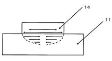
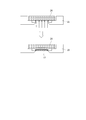
- FIG. 3 is an example of a member for controlling a growth portion of a group III nitride crystal on a single crystal base substrate. It is the schematic diagram which showed the distribution and the direction of the thermal stress concerning the inside of the group III nitride crystal laminated body under cooling with the arrow. It is sectional drawing which shows an example of a board
- FIG. 1 and 2 are diagrams showing an example of a specific manufacturing process of the present invention.
- the present invention is obtained by growing a group III nitride single crystal including a group III nitride single crystal layer 12 on a single crystal base substrate 11 by growing a group III nitride single crystal by vapor phase growth.
- a group III nitride crystal substrate 18 composed of a group III nitride crystal layer 14 by collecting a group III nitride crystal 17 from the laminated body 15 comprising: 1) Select a substrate having a smaller thermal expansion coefficient than the group III nitride single crystal layer 12 as the single crystal base substrate 11; 2) The growth portion 16 of the group III nitride single crystal layer 12 is set to an area at least 5.0 mm or more from the outer periphery of the single crystal base substrate 11; 3) A laminate 15 is manufactured so that the thickness of the group III nitride crystal layer 14 is 100 ⁇ m or more, 4) The laminated body 15 is cooled to cause cracks in the single crystal base substrate 11 to separate the group III nitride crystal body 17, 5) Next, the group III nitride crystal substrate 18 is manufactured by removing the piece of the single crystal base substrate 11 attached to the separated group III nitride crystal body 17.
- the growth method of the group III nitride crystal layer 14 on the single crystal base substrate 11 which is a single crystal is easy to form a single crystal layer and to easily control the film thickness, and further laminated on the layer as necessary.
- a vapor phase growth method is employed.
- Specific examples of the method include known vapor phase growth methods such as the sputtering method, PLD (Pulse Laser Deposition) method, and sublimation recrystallization method in addition to the HVPE method, MOVPE method, and MBE method described above.
- the group III nitride includes not only single metal nitrides such as AlN, GaN and InN but also composite metal nitrides such as AlGaN and InAlGaN.
- a halide of a group III metal atom and a nitrogen source gas which are raw materials, are introduced, a reaction is caused on a single crystal base substrate, and a target crystal is grown.
- halides of group III metal atoms halogen metal compounds such as aluminum halides such as AlCl 3 , AlCl and AlBr 3 and gallium halides such as GaCl 3 are used, but mixed metal nitrides such as AlGaN are mixed. When obtaining crystals, these halogen metal compounds are appropriately mixed and used according to the composition of the target crystals.
- the nitrogen source gas ammonia, hydrazine, or the like is used.
- These source gases are usually mixed with a gas called a carrier gas and supplied onto the base substrate for the purpose of controlling the residence time in the vicinity of the single crystal base substrate and preventing turbulent flow.
- a carrier gas nitrogen, hydrogen, rare gases such as helium and argon, and mixed gases thereof are generally used, and the volume ratio is generally in the range of about 10 to several thousand times that of the source gas. Is done.
- organic metal is used as the raw material to supply group III atoms, ammonia, hydrazine, amines, etc. are used as the nitrogen source gas. Both are mixed in the carrier gas and reacted on the single crystal base substrate. To grow the desired crystal.
- Various molecular structures of organic metals are conceivable, and an appropriate raw material is selected according to the reaction rate predicted from the boiling point, chemical stability, etc., and the compatibility of the device design. Recently, trimethylaluminum is often used as an organic aluminum raw material, and trimethylgallium is used as an organic gallium raw material.
- the Group III raw material is kept as a single substance in a cell placed around the high vacuum chamber, and is supplied into the chamber by opening and closing the shutter.
- nitrogen raw materials excite nitrogen gas at a high frequency to generate radical nitrogen atoms, which are supplied by opening and closing the shutter.
- the sputtering method is a method of implanting argon or nitrogen atoms ionized into a metal target in a vacuum chamber to blow off the metal atoms to form a film at a predetermined place.
- Group III nitride crystals are produced by a method that targets group III nitride itself, or a reactive sputtering method in which a group III metal is used as a target and a nitrogen-containing gas is supplied to react before deposition on the base substrate. Industrial methods are being considered.
- the sublimation recrystallization method is a method in which a gas phase of group III nitride is generated at a high temperature portion in a furnace in which a temperature gradient is formed, and is deposited on a seed crystal or a single crystal base substrate installed in the low temperature portion.
- the group III nitride is also thermally decomposed and moved in the state of group III metal vapor and nitrogen at the same time. Therefore, this process is generally called a chemical transport method.
- the selection of the single crystal base substrate 11 and the group III nitride single crystal layer 12 to be grown on the single crystal base substrate, the determination of the growth portion 16 on the single crystal base substrate 11, the group III nitride crystal layer This can be achieved by limiting the thickness of 14, and any of the above vapor phase growth methods may be employed.
- the HVPE method is preferred.
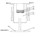
- a typical apparatus used in the HVPE method is an apparatus schematically shown in FIG. Specifically, as described in Japanese Patent Application Laid-Open No. 2006-290662, a reactor main body 21 composed of a cylindrical quartz glass reaction tube, an external heating means 23 disposed outside the reaction tube, The apparatus includes a local heating device 22 and a holding susceptor 25 disposed inside the reaction tube. In this apparatus, the carrier gas and the raw material gas are supplied from one end of the reaction tube, and the carrier gas and the unreacted reaction gas are discharged from the opening provided in the side wall near the other end. ing.
- two gas supply lines 26 and 27 are provided on the gas supply side of the reaction tank, and aluminum trichloride gas and carrier gas are supplied from one channel outlet (also referred to as a halide gas supply nozzle). And a mixed gas of ammonia gas as nitrogen source gas and hydrogen gas as carrier gas is supplied from the other channel outlet (also referred to as nitrogen source gas supply nozzle).
- the external heating means is not intended to heat the single crystal base substrate, but is mainly used for the purpose of maintaining the temperature of the reaction gas in the reaction zone at a predetermined temperature, and is not necessarily essential. Absent. As this external heating means, a resistance heating heater, a high frequency heating device, a high frequency induction heating device, a lamp heater, or the like can be used. Further, the local heating device and the holding susceptor can hold the single crystal base substrate 24 and heat it to about 1600 ° C.
- the present invention it is important to select a single crystal substrate as a base substrate for growing the group III nitride crystal layer including the group III nitride single crystal layer. That is, a substrate having a smaller thermal expansion coefficient than the group III nitride single crystal layer must be selected as the single crystal base substrate.
- the present invention is not intended for the case where the single crystal base substrate and the group III nitride crystal layer have the same thermal expansion coefficient, for example, the case where the single crystal base substrate and the group III nitride crystal layer are made of the same material. .
- the problem of the present invention does not occur.
- the present invention is directed to the case where the single crystal base substrate and the group III nitride crystal layer have different thermal expansion coefficients, for example, the case where the single crystal base substrate and the group III nitride crystal layer are made of different materials. is there.
- the thermal expansion coefficient of the single crystal base substrate is 95% or less of the thermal expansion coefficient of the group III nitride single crystal layer.
- the lower limit of the thermal expansion coefficient of the single crystal base substrate is not particularly limited, but for the purpose of avoiding excessive thermal stress, the thermal expansion coefficient of the single crystal base substrate is the heat of the group III nitride single crystal layer. It is desirable to be 50% or more of the expansion coefficient.
- a complex group III nitride crystal such as AlGaN, it is difficult to predict the change in physical property value due to the composition ratio, and therefore a material conforming to AlN should be adopted.
- the single crystal base substrate to be used preferably has a smooth surface to be laminated in order to directly laminate a group III nitride single crystal of good quality and controlled orientation. Therefore, a general single crystal base substrate for epitaxial growth is preferably used.
- the thickness of the single crystal base substrate to be used is arbitrarily selected without any particular limitation, but in order to suppress deformation caused by lattice constant mismatch while laminating group III nitride crystals,
- the thickness is preferably sufficient to give sufficient rigidity to the base substrate. From this viewpoint, the thickness is preferably 600 ⁇ m or more, and particularly preferably 800 ⁇ m or more.
- the upper limit of the thickness of the single crystal base substrate to be used is not particularly limited, but is 5000 ⁇ m in consideration of industrial production.
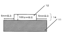
- the group III nitride single crystal growth portion needs to be an area at least 5.0 mm inside from the outer periphery of the single crystal base substrate. If the growth part is 5.0 mm or more inside from the outer periphery, the following effects are exhibited. Therefore, it is disadvantageous to make the region more inside from the viewpoint of effective use of the single crystal base substrate. Therefore, it is essential to make the growth part a region that is 5.0 mm or more inside from the outer periphery, and it is sufficient that the region is 5.2 mm or more inside.
- the growth region extends from the outer periphery of the single crystal base substrate to a region less than 5.0 mm, the boundary between the portion where the group III nitride single crystal layer of the base substrate has grown and the portion where it has not grown by the mechanism described later Stress concentration does not occur sufficiently, and the selective crack inside the single crystal base substrate, which is the effect of the present invention, does not occur, and the group III nitride single crystal layer is cracked.
- the area at least 5.0 mm or more from the outer periphery refers to an area on the substrate center side that leaves at least 5.0 mm or more of the substrate surface from the outer periphery.
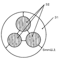
- the region 32 in FIG. 6 is referred to as a growth portion
- the region 32 in FIG. 7 is referred to as a growth portion
- the shape of the growth portion region satisfies the above requirements.
- the number of growth portions is not limited as long as it is in the above-described region, and a plurality of portions can be provided according to the size of the target single crystal base substrate as in the region 32 in FIG.
- it is essential for the same reason that the distance between the growth part is 5.0 mm or more.
- the most reliable method for making the group III nitride single crystal growth region at least 5.0 mm or more from the outer periphery of the single crystal base substrate is to deposit the mask material using lithography technology
- a method of covering a part of the surface of the single crystal base substrate with a member having resistance to the growth temperature and source gas is simple. That is, the above-mentioned object can be achieved by preparing a member capable of covering at least the entire single crystal base substrate and then placing the growth portion in the shape corresponding to the shape on the single crystal base substrate ( FIG. 9).
- a vapor phase growth apparatus with the growth surface facing downward or sideways uses a susceptor that adjusts the shape of the fixed part that fixes the single crystal base substrate so that the growth part region satisfies the above conditions. (25 in FIG. 3).
- a susceptor that adjusts the shape of the fixed part that fixes the single crystal base substrate so that the growth part region satisfies the above conditions.
- a crystal grows, and then a crack is generated, and the obtained group III nitride crystal may fall due to its own weight.
- a space for the reaction gas to flow is provided in a part on the opening side of the susceptor so that the diameter of the grown crystal is larger than the diameter of the opening formed by the susceptor. It is preferable.
- the size of the group III nitride crystal depends on the reaction conditions such as the shape and size of the opening, the size of the space gap, the flow rate of the reaction gas, and the reaction temperature. It is necessary to know in advance whether it will spread.
- the lower limit of the growth region is not particularly limited, but in order to efficiently use a single crystal base substrate and increase the productivity of the group III nitride crystal layer, the total area of the growth region is It is suitable to design so as to be 10% or more, preferably 60% or more and 99% or less with respect to the entire area of the main surface of the base substrate.
- the thickness of the group III nitride crystal layer 14 grown and laminated on the single crystal base substrate 11 is 100 ⁇ m or more. From the viewpoint of strength when the obtained group III nitride crystal layer is used as a self-supporting substrate, the thickness is preferably 150 ⁇ m or more.
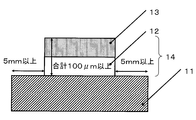
- the group III nitride crystal layer 14 will be described in detail below, but may be composed of only the group III nitride single crystal 12 as shown in FIG. 4, or the group III nitride as shown in FIG.
- the group III nitride polycrystalline layer 13 may be laminated on the single crystal 12.
- the group III nitride single crystal layer of the single crystal base substrate is formed by a mechanism described later. Stress concentration hardly occurs at the boundary between the grown portion and the ungrown portion. As a result, breakage propagates to the group III nitride crystal or cracks are introduced. Even if these adverse effects are avoided, the group III nitride crystal to be collected and the group III nitride crystal substrate obtained by processing the same have large warpage, so that the group III nitride single crystal vapor phase growth can be performed. The quality is not sufficient as a single crystal base substrate.
- the upper limit of the thickness of group III nitride crystal layer 14 is not particularly limited, but is 500 ⁇ m in view of industrial production.
- the structure of the group III nitride crystal layer having a thickness of 100 ⁇ m or more is that if the layer directly in contact with the single crystal base substrate is a group III nitride single crystal layer, the crystal layer above it is polycrystalline even if it is a single crystal. There may be. When it consists of only a single crystal, the layer will be 100 micrometers or more. When a polycrystalline layer is laminated on a single crystal layer, the total thickness needs to be 100 ⁇ m or more. In the latter case, it is preferable to set the thickness of the single crystal layer to 0.1 ⁇ m or more and 0.3 ⁇ m or less because crack introduction can be avoided almost certainly regardless of the conditions for polycrystalline deposition.
- a group III nitride crystal substrate made of a group III nitride single crystal can be obtained simply by removing the base substrate after separation.
- the growth temperature may be limited in view of the melting point of the single crystal base substrate and the reaction between the base substrate and the group III nitride single crystal, and it takes a very long time to achieve a thickness of 100 ⁇ m or more with only the single crystal. This tends to occur.
- the group III nitride crystal layer has a double-layer structure of single crystal and polycrystal
- the growth of the polycrystal is performed under a lower temperature condition than that of the single crystal as described later. Since it can be grown at high speed, it can be manufactured in a short time, and the energy cost can be reduced accordingly.
- defects are easily generated and moved at the grain boundaries formed in the polycrystalline layer, so that the obtained group III nitride crystal substrate is difficult to break, and the yield after the next process is high. It also has the advantage of improving.
- the group III nitride crystal layer preferably has a two-layer structure in which a polycrystalline layer is stacked on a single crystal layer. Note that when an attempt is made to grow a polycrystal under extremely low temperature conditions, it takes a so-called amorphous form that does not take the form of crystal grains. In this embodiment, the same effect can be obtained. However, since the chemical resistance is relatively low, it is necessary to examine conditions so that the single crystal substrate for growth is not lost together when the growth single crystal substrate is removed by chemical treatment.
- a group III nitride crystal layer may be grown on a single crystal base substrate so as to satisfy the above conditions.
- the conditions for growing the group III nitride crystal layer may be adjusted by adjusting the supply conditions of the source gas, the temperature during the growth, etc. in each vapor phase growth method. Even when the group III nitride crystal layer is composed of a group III nitride single crystal layer and a group III nitride polycrystalline layer, the manufacturing conditions may be adjusted in each vapor phase growth method.
- a method for growing a group III nitride crystal layer by the HVPE method suitably employed in the method of the present invention will be described.
- the group III nitride will be described using a typical example of aluminum nitride (AlN).
- the base substrate is heated for about 10 minutes at a high temperature of about 1100 ° C. for the purpose of removing organic substances adhering to the surface of the single crystal base substrate. Preferably it is done. More desirably, it is preferably performed at 1200 ° C. or higher for 30 minutes or longer.
- Thermal cleaning may be performed by either an external heating device or a heating support. After the thermal cleaning, the temperature of the single crystal base substrate is heated to 800 ° C. to the substrate melting point, preferably 1000 ° C. to a temperature lower than the substrate melting point by 100 ° C., and the supply of various source gases is started. Form a layer.
- the reason why the temperature slightly lower than the melting point of the substrate is preferable is that the atoms constituting the base substrate are very easy to move near the melting point, so that the atomic arrangement on the surface is disturbed or the group III nitride crystal is grown. This is because an adverse effect of diffusing into the surface and disturbing the shape of the interface occurs.
- the supply amount of the aluminum trichloride gas is appropriately determined in consideration of the crystal growth rate on the single crystal base substrate.
- the nitrogen source gas is supplied so that the number of nitrogen atoms is 1 or more times the supply amount of aluminum atoms (hereinafter, this magnification is also referred to as V / III ratio).
- Aluminum trichloride gas can be obtained by reacting aluminum metal with hydrogen halide or chlorine. Specifically, for example, it can be produced by the method described in JP-A-2003-303774. Moreover, it can also manufacture by heating and vaporizing solid aluminum trichloride itself. In this case, it is preferable to use aluminum trichloride which is an anhydrous crystal and has few impurities.
- the nitrogen source gas a reactive gas containing nitrogen is adopted, but ammonia gas is preferable in terms of cost and ease of handling.
- the aluminum halide gas and the nitrogen source gas are each diluted to a desired concentration with a carrier gas and introduced into the reaction vessel.
- hydrogen, nitrogen, helium, or a single gas of argon, or a mixed gas thereof can be used as a carrier gas, and an impurity gas component such as oxygen, water vapor, carbon monoxide, or carbon dioxide using a purifier in advance. Is preferably removed.
- the AlN single crystal layer alone is used as the AlN crystal layer (when the AlN single crystal layer 12 is 100 ⁇ m or more), it is preferable to select conditions for increasing the growth rate of the single crystal among the above conditions.
- a high temperature preferably 1250 ° C. or higher, more preferably 1350 ° C. or higher is desirable.
- the reaction vessel is made of quartz, the service temperature is only about 1150 ° C. Therefore, when heating to a temperature higher than this temperature, the reaction vessel should be heated as disclosed in JP-A-2006-290662. It is preferable to employ a mechanism for heating only the growing AlN single crystal film.
- the upper limit of the temperature at the time of growing the AlN single crystal is 1700 ° C. in consideration of operability and the thermal decomposition reaction rate of the AlN single crystal and the substrate holding member.
- High speed growth of an AlN single crystal can be realized by performing the procedure taught in Japanese Patent Application Laid-Open Nos. 2006-1114845 and 2008-88048 after satisfying the above requirements.
- a group III nitride crystal laminate in which the group III nitride crystal layer is laminated on the base substrate can be manufactured by the above method.
- a growth method when the group III nitride crystal layer has a two-layer structure of a single crystal layer and a polycrystalline layer will be described.
- the conditions must generally be determined in consideration of the growth thickness of the single crystal and the growth efficiency in that case.
- the growth thickness of the crystal layer is in the range of 0.1 ⁇ m to 0.3 ⁇ m as described above, it is not always necessary to use conditions suitable for high-speed growth.
- the lamination of the group III nitride polycrystalline layer on the group III nitride single crystal layer is performed under the condition that deviates from the above-mentioned single crystal growth conditions.
- the shift to the high temperature condition side is not appropriate because it leads to melting of the single crystal base substrate.
- Effective operations include a method of lowering the temperature at which single crystal growth is difficult, or increasing the amount of raw material supply to several to several tens of times. In particular, an increase in the raw material supply amount is preferable because it leads to an improvement in the growth rate of the polycrystalline layer.
- an AlN polycrystal layer is formed on an AlN single crystal layer by the HVPE method
- the raw material supply amount is adjusted so that the growth rate is at least 20 ⁇ m / Hr at 1000 ° C. and at least 10 ⁇ m / Hr at 800 ° C. Switching from crystal growth to polycrystalline growth is realized.
- an AlN polycrystal layer can be formed on an AlN single crystal layer, and a laminated body in which a group III nitride crystal layer having a two-layer structure is laminated on a single crystal base substrate is manufactured. be able to.
- the laminated body is generally manufactured at a temperature of 1100 ° C. or higher, although depending on the conditions of the vapor phase growth method.
- the inside of the single crystal base substrate is selected from the boundary between the portion where the group III nitride single crystal layer has grown and the portion where it has not grown. Cracks occur and the group III nitride crystals spontaneously separate. This separation mechanism is considered as follows.
- the method for cooling the laminate is not particularly limited, and examples thereof include a method for cooling the inside of the reaction tube, for example, a method for stopping heating of crystal growth and flowing a carrier gas into the reaction apparatus.
- a method for cooling the inside of the reaction tube for example, a method for stopping heating of crystal growth and flowing a carrier gas into the reaction apparatus.
- the nitrogen source gas flows through the reaction vessel until the temperature of the substrate falls below 800 ° C. It is desirable.
- the cooling rate of the laminate is appropriately selected depending on the difference in thermal expansion coefficient and the breaking strength between the single crystal base substrate and the group III nitride crystal, but prevents the thermal shock cracking of the group III nitride crystal, and further the single crystal
- the temperature is preferably 5 ° C./min to 50 ° C./min, and more preferably 10 ° C./min to 30 ° C./min.
- the laminate is cooled within the cooling rate range until the temperature range is 300 to 500 ° C. or less from the temperature range during growth. It is preferable to cool while maintaining the speed.
- the group III nitride crystal obtained by cooling is cracked in the single crystal base substrate to be separated, so that a part of the single crystal base substrate is attached.
- the attached single crystal base substrate can be removed by a conventionally known method, for example, a dissolution and removal method of selectively dissolving with an acid or alkali solution, or a polishing removal method of polishing with a diamond grindstone or diamond slurry.
- a dissolution and removal method of selectively dissolving with an acid or alkali solution or a polishing removal method of polishing with a diamond grindstone or diamond slurry.
- the single crystal base substrate can be easily separated and the group III nitride crystal compared with the conventional method.
- a substrate can be manufactured.
- the dissolution removal method will be described as an example.
- an acid solution such as a mixed acid of hydrofluoric acid and nitric acid
- an alkali solution such as a sodium hydroxide aqueous solution, a potassium hydroxide aqueous solution, or a tetramethylammonium hydroxide aqueous solution is used as the solution. It is done.
- these alkali solutions also dissolve group III nitrides in general, attention must be paid to the immersion method and concentration.
- the dissolution time depends on the concentration of the chemical solution and the amount of the attached single crystal base substrate, but the ratio of 48 mass% hydrofluoric acid, 70 mass% nitric acid, high purity acetic acid, and ultrapure water is a volume ratio of 2: 1: 1: 1.
- the group III nitride crystal of the present invention may be usually dissolved for about 0.5 to 2 hours.
- a group III nitride crystal substrate is obtained by removing the single crystal base substrate adhering to the group III nitride crystal. Since the substrate effectively suppresses thermal stress generated during growth and cooling by various devices, a base substrate for producing a self-supporting substrate having a single crystal portion that is free from breakage, cracks, and warpage, Or it can be a free-standing substrate.
- a method of performing contact measurement with a micrometer on the group III nitride crystal substrate after the removal of the single crystal base substrate is simple. Since the contact-type measurement may damage the crystal surface, a three-dimensional shape measuring apparatus capable of measuring the thickness after irradiating laser from both sides and excluding the influence of warpage may be used. For breaks and cracks, a differential interference microscope is used to make the step visible, and if it is not visually recognized, there will be no hindrance to the use described later. The amount of warpage can be easily measured with an optical interference microscope, a laser interferometer, or the like, and is generally evaluated by a radius of curvature or its reciprocal.
- the group III nitride crystal substrate obtained by the present invention is considered to be applicable to uses described later as long as the radius of curvature is 1 m or more, and it is possible to produce a substrate exceeding 10 m.
- the group III nitride crystal substrate obtained by the present invention can be used as a self-standing substrate for stacking ultraviolet light emitting elements, but the group III nitride single crystal of the substrate is exposed.
- a thick group III-nitride single crystal substrate having excellent crystallinity can be obtained by growing a group III nitride single crystal on the single crystal using the surface thus formed as a base. Next, a method for manufacturing the group III nitride single crystal substrate (free-standing substrate) will be described.
- the above-described various vapor phase growth methods and conditions are employed.
- the base substrate used for single crystal growth originally needs a planarization step corresponding to the CMP polishing process.
- the RMS value already has a value in the order of nm when the single crystal substrate for growth is removed. Since the good surface which shows is already obtained, the conventional process can be skipped.
- the polycrystalline layer portion is removed by a known method, for example, a wire saw Or by using a cutting method using a diamond cutter or a grinding method using a surface grinder. As a result, a group III nitride single crystal substrate composed only of the group III nitride single crystal is obtained.
- the group III nitride crystal substrate consisting only of the group III nitride single crystal thus obtained, or the group III nitride single crystal substrate has a strength that can withstand handling as a free-standing substrate if it has a thickness of 100 ⁇ m or more. Have. Therefore, the obtained group III nitride single crystal substrate having a thickness of several hundreds of ⁇ m or more is further cut into thin substrates to produce a plurality of group III nitride single crystal substrates (base substrate), or A thinly cut substrate can be used as a self-supporting substrate.
- the existing non-oxide ceramic processing technology can be used without limitation for the method of cutting the group III nitride single crystal substrate, a method that reduces the amount of wear during processing is desirable, and a cutting method using a wire saw or a diamond cutter is preferable. is there.
- the obtained group III nitride single crystal substrate is self-supported for stacking an ultraviolet light emitting element after heat treatment in a nitrogen atmosphere or a reducing atmosphere or after performing post-treatment such as surface cleaning with aqua regia. It can be used as a substrate or a growth substrate (base substrate) for re-growing a group III nitride single crystal.
- EXAMPLES Hereinafter, although an Example demonstrates this invention further in detail, this invention is not limited to these Examples. In addition, not all combinations of features described in the embodiments are essential to the solution means of the present invention.
- Example 1 In this example, an aluminum nitride single crystal and a polycrystal were grown using the reactor shown in FIG. 3, and then an aluminum nitride crystal substrate was obtained after cooling.
- the susceptor a susceptor having a 1 mm gap (gap between the susceptor and the base substrate) formed in the opening shown in FIG. 11 was used.
- the group III compound supply pipe (26) is provided with a reaction furnace in which metal aluminum pellets are placed upstream and heated to 500 ° C., and hydrogen chloride gas is supplied to generate aluminum trichloride gas. Ammonia was supplied from the nitrogen raw material supply pipe (27), and both pipes were heated to 200 ° C. or higher while the raw material was flowing.
- the external heating device (23) was not used as a heat source.
- a single crystal substrate for silicon growth having a ⁇ 1 1 1 ⁇ plane as a main surface was used as a single crystal base substrate.
- the dimensions are 50.8 mm (2 inches) in diameter and 1.0 mm in thickness.
- the surface that was subjected to the CMP polishing treatment was defined as a group III nitride growth surface.
- This base substrate was immersed in a 5 mass% hydrofluoric acid aqueous solution for 30 seconds to remove the oxide film and to perform a hydrogen termination treatment.
- a holding susceptor (25) made of pyrolytic boron nitride having a circular shape with a diameter of 26 mm, with the opening located in the center, with the single crystal base substrate positioned at 24 in FIG. 3 with the growth surface facing downward. Fixed with.
- the distance from the single crystal base substrate end to the opening end is 12.4 mm.
- the pressure was once reduced to 1 Torr or lower, and after returning to atmospheric pressure with nitrogen gas, the pressure was again reduced to 1 Torr or lower to discharge air.
- hydrogen was introduced from the group III compound supply pipe and the nitrogen material supply pipe, the pressure was restored to atmospheric pressure, the local heating device (22) was energized, and heating was started at 20 ° C./min.
- the gas flow rate here refers to the total of the hydrogen flow rate during heating and cooling, the hydrogen flow rate during growth, and the raw material gas flow rate.
- the raw material was held without flowing for 5 minutes to stabilize the temperature distribution, and then the supply of aluminum trichloride gas was resumed to start growth.
- the supply rate was 1.0 ⁇ 10 ⁇ 2 atm for both aluminum trichloride gas and ammonia gas to promote high-speed growth.
- the supply of aluminum trichloride gas was stopped again and cooling was started at 20 ° C./min.
- the temperature dropped to 800 ° C. the supply of ammonia gas and hydrogen gas was stopped, and the cooling was continued by switching to nitrogen gas at the same flow rate.
- the output of the local heating device was turned off and the system was allowed to cool without changing the flow rate of nitrogen gas.
- the aluminum nitride crystal was separated from the single crystal base substrate together with part of the base substrate.
- the crystal growth was performed with the growth surface facing downward.
- the spontaneously separated aluminum nitride crystal had almost the same shape as the opening of the holding susceptor, and the average diameter was 28 mm.
- This is immersed in a chemical solution in which 48 mass% hydrofluoric acid, 70 mass% nitric acid, high purity acetic acid, and ultrapure water are mixed at a volume ratio of 2: 1: 1: 1 for 1 hour, By chemically removing, an aluminum nitride crystal substrate composed of a combination of a single crystal layer and a polycrystalline layer was obtained.
- the thickness was 213 ⁇ m, and the growth rate of the polycrystalline layer in this example was 141.8 ⁇ m / hour.
- the weight was 0.3127 g, and silicon adhering during spontaneous separation was 0.2913 g.
- Example 2 In this example, the central opening of the susceptor is made larger than that in Example 1, and a large-area aluminum nitride crystal substrate is manufactured.
- the other experimental conditions were the same as in Example 1.
- As the single crystal base substrate a single crystal substrate for silicon growth having a ⁇ 1 1 1 ⁇ plane as a main surface was used. The dimensions are 50.8 mm (2 inches) in diameter and 1.0 mm in thickness.
- a treatment for enlarging the growth region was performed with the opening located at the center of the pyrolytic boron nitride susceptor holding the substrate having a diameter of 40 mm. The distance from the single crystal base substrate edge to the opening edge is 5.4 mm.
- the aluminum nitride crystal with a part of the single crystal base substrate was recovered in the same manner as in Example 1 while maintaining the shape of ⁇ 40 mm in the growth part.
- the base substrate side had a recess that matched the shape of the silicon peeled off accompanying the aluminum nitride laminate, and the substrate was recovered without breaking into multiple pieces.
- the aluminum nitride crystal substrate after the base substrate was dissolved by the mixed acid had no evidence of cracks or breaks on the surface of the single crystal layer, and formed a flat surface having gloss as in Example 1.
- the radius of curvature of the aluminum nitride crystal substrate obtained in this example had a distribution of -3.6 m in the central diameter range of 20 mm and -1.9 m on the outer periphery. However, conditions sufficient for practical use were satisfied, and the flatness of the surface was sufficiently secured at 2.2 nm in terms of RMS value.
- the thickness was 225 ⁇ m at the center, 190 ⁇ m near the outer periphery, the weight was 0.7732 g, and the silicon deposited during spontaneous separation was 0.6006 g. In order to completely dissolve the adhered silicon, 50 mL of hydrofluoric acid was required, and the time required for dissolution was 95 minutes.
- Example 3 an aluminum nitride crystal substrate was manufactured using a single crystal base substrate that was thinner than the single crystal base substrate used in Example 1, and the other experimental conditions were the same as in Example 1. .
- the single crystal base substrate a single crystal substrate for silicon growth having a ⁇ 1 1 1 ⁇ plane as a main surface was used. The dimensions are 50.8 mm (2 inches) in diameter and 0.28 mm in thickness.
- the laminated body after cooling was recovered in the same manner as in Example 1 with the aluminum nitride crystal body including a part of the single crystal base substrate remaining in the shape of ⁇ 26 mm of the growth part.
- the single crystal base substrate was thin, it was not a rupture that was peeled off from the base substrate as in Example 1, but a shape in which a crack penetrated the single crystal base substrate and was cut into a circle.
- the outer peripheral base substrate had radial cracks and was broken into eight.
- the aluminum nitride crystal substrate after the single crystal base substrate was dissolved by the mixed acid had no evidence of cracks or breaks on the surface of the single crystal layer, and formed a flat surface having gloss similar to that of Example 1.
- the radius of curvature of the aluminum nitride crystal substrate obtained in this example is -1.2 m, which is more distorted than in Example 1. there were.
- the flatness of the surface was ensured, and the RMS value was 2.9 nm.
- the thickness was 215 ⁇ m, the weight was 0.3195 g, and the silicon deposited during spontaneous separation was 0.3411 g.
- To completely dissolve the adhered silicon 30 mL of hydrofluoric acid was required, and the time required for dissolution was 70 minutes.
- Example 4 the aluminum nitride crystal substrate obtained in Example 1 was used as a base substrate, and an aluminum nitride single crystal was further grown thereon, and after the growth, the polycrystalline portion was removed to produce an aluminum nitride single crystal substrate.
- the base substrate used for single crystal growth requires a planarization step corresponding to the conventional CMP polishing process.
- a good surface showing an RMS value on the order of nm has already been obtained.
- the conventional process was omitted.
- the same apparatus as used in Example 1 was used for crystal growth, and the holding susceptor made of pyrolytic boron nitride was changed to one having an opening of 22 mm in diameter to prevent the growth substrate from falling.
- the supply method such as generation method of aluminum trichloride gas and pipe temperature control was the same.
- the heating rate was the same, but the gas supplied during the heating was mixed with ammonia at a partial pressure of 5.0 ⁇ 10 ⁇ 4 atm in addition to hydrogen gas. This prevents the thermal decomposition of the aluminum nitride and preserves the aluminum nitride single crystal layer on the surface.
- the AlN single crystal growth temperature was heated to 1400 ° C., and the aluminum trichloride gas was held without flowing for 40 minutes to stabilize the temperature distribution, and then the supply of aluminum trichloride gas was started.
- Nitrogen trichloride gas and ammonia gas are mixed in hydrogen, which is a carrier gas, and sprayed onto the base substrate so that both the aluminum trichloride gas and ammonia gas are 5.0 ⁇ 10 ⁇ 3 atm, and both are reacted on the base substrate for nitriding
- Aluminum single crystals were synthesized. After maintaining in this state for 1200 minutes, the supply of aluminum trichloride gas was stopped, and the flow was continued without changing the supply amount of only ammonia gas, and the mixture was cooled to 800 ° C. at 20 ° C./min. When the temperature dropped to 800 ° C., the supply of ammonia gas and hydrogen gas was stopped as in Example 1, and the cooling was continued by switching to nitrogen gas at the same flow rate. After cooling to 500 ° C., the output of the local heating device was turned off and the system was allowed to cool without changing the flow rate of nitrogen gas.
- the growth surface after cooling had a shape in which hexagonal pyramids were spread, and the directions were uniform.
- the result of Example 1 was changed from ⁇ 2.7 m to +4.5 m. This is considered to be a phenomenon that occurs because the polycrystalline layer of the base substrate is irregular in the a-axis and c-axis of aluminum nitride and has a slightly larger thermal expansion coefficient than the a-axis direction of the single crystal layer. The occurrence of breakage and cracks due to this difference in thermal expansion coefficient was not confirmed.
- the total thickness of the base substrate and the growth layer measured with a micrometer was 1033 ⁇ m, and the average growth rate over 20 hours was 41 ⁇ m per hour.
- the laminated body was embedded in an epoxy resin, and the polycrystalline layer side was ground together with the epoxy resin with a surface grinder to remove the polycrystalline layer. Thereafter, polishing with diamond slurry was performed on both sides to prepare the shape as a substrate.
- the thickness of the aluminum nitride single crystal substrate after this step was 340 ⁇ m.
- Example 5 an aluminum nitride crystal substrate was manufactured by replacing the single crystal base substrate with a material other than single crystal silicon.
- the other experimental conditions were the same as in Example 1.
- As the single crystal base substrate a silicon carbide growth single crystal substrate having a ⁇ 0 0 0 1 ⁇ plane as a main surface was used. The dimensions are 50.8 mm (2 inches) in diameter and 0.26 mm in thickness.
- the thermal expansion coefficient of aluminum nitride 4.2 ppm / ° C.
- the thermal expansion coefficient of silicon carbide is 2.8 ppm / ° C., which satisfies the conditions of the base substrate required in the present invention.
- the aluminum nitride crystal accompanied with a part of the single crystal base substrate was recovered in the same manner as in Example 1 while maintaining the shape of ⁇ 26 mm in the growth part.
- a portion having a recess that matches the shape of the silicon carbide peeled off accompanying the aluminum nitride laminate is cut into a circular shape, and the single crystal base substrate on the outer periphery has three radial cracks. It was cracked.
- the silicon carbide adhering at the time of spontaneous separation was 0.0627 g.
- a three-stage treatment was performed.
- a polishing process was performed to remove a step of several ⁇ m or more.
- carbon tetrafluoride and oxygen were supplied in a reactive ion etching apparatus to generate reactive plasma, and etching was performed until the remaining silicon carbide was 0.0050 g or less.
- the surface oxidation treatment for supplying only oxygen and the oxide film removal treatment by 48 mass% hydrofluoric acid immersion were repeated to expose the aluminum nitride single crystal layer.
- the radius of curvature of the aluminum nitride crystal substrate obtained in this example was ⁇ 1.3 m, which was the same as that obtained when single crystal silicon having substantially the same shape was used as the base substrate.
- the flatness of the surface was impaired by the plasma treatment damage, and the RMS value was 30.8 nm.
- Comparative Example 1 In this example, a single-crystal base substrate was tried to collect an aluminum nitride crystal substrate in place of a material whose thermal expansion coefficient relationship with the group III nitride crystal to be grown does not satisfy the present invention. The conditions were the same as in Example 1.
- As the single crystal base substrate an ⁇ -alumina growth single crystal substrate (sapphire substrate) having a ⁇ 0 0 0 1 ⁇ plane as a main surface was used. The dimensions are 50.8 mm (2 inches) in diameter and 0.43 mm thickness.
- the coefficient of thermal expansion of sapphire is 7.0 ppm / ° C., which is opposite to the base substrate conditions required in the present invention.
- the laminated body after cooling was recovered in a shape broken to 6 pieces from the center together with the sapphire substrate.
- the sapphire substrate has a larger coefficient of thermal expansion than aluminum nitride, and because the compressive stress is applied to the sapphire substrate side at the boundary between the growth part and the non-growth part that started breaking in Example 1, it failed to induce the breakage point. It is thought that random fracture occurred on the entire substrate. Further, since sapphire has a very high chemical resistance, the surface after separation of the single crystal base substrate could not be confirmed.
- the growth region was expanded to a region within 5.0 mm from the outer periphery, and the other experimental conditions were the same as in Example 1.
- the single crystal base substrate a single crystal substrate for silicon growth having a ⁇ 1 1 1 ⁇ plane as a main surface was used. The dimensions are 50.8 mm (2 inches) in diameter and 1.0 mm in thickness.
- a treatment for enlarging the growth region was performed with the opening located in the center of the pyrolytic boron nitride susceptor holding the substrate having a diameter of 48 mm.
- the non-growth portion on the single crystal base substrate is a region from the outer periphery to 1.4 mm.
- the laminated body after cooling was recovered in such a manner that the spontaneous separation of the single crystal base substrate and the aluminum nitride crystal, which had been completed in Example 1, was stopped halfway.
- the starting points of the cracks for spontaneous separation varied from the main surface of the substrate to the side surface of the substrate, and these cracks stopped near the center of the substrate.
- On the side where no cracks occurred there was no escape site for thermal stress, so cracks occurred on both the single crystal base substrate and the aluminum nitride crystal.
- the single crystal base substrate where the cracks for spontaneous separation progressed and the part where the crack did not progress soon separated and spontaneously separated locally. It became a shape.
- the aluminum nitride crystal substrate after dissolution of the single crystal base substrate had a flat single crystal layer surface as in Example 1. However, a fracture occurred at the position of the crack generated at the time of recovery, and a disk with a maximum diameter of 48 mm was almost formed. Only semi-circular aluminum nitride crystals divided into half were collected. Since it was necessary to dissolve the entire 1.0-mm thick single crystal base substrate, 110 mL of hydrofluoric acid was required to completely dissolve the silicon of this laminate, which was required for dissolution. The time was 11 hours.
- the thickness of the growth crystal part of the aluminum nitride laminate was set to 100 ⁇ m or less, and the other experimental conditions were the same as in Example 1.
- the single crystal base substrate a single crystal substrate for silicon growth having a ⁇ 1 1 1 ⁇ plane as a main surface was used. The dimensions are 50.8 mm (2 inches) in diameter and 1.0 mm in thickness.
- the equipment used, the method of generating aluminum trichloride gas, the piping temperature control, etc. were also the same.
- the conditions necessary for AlN single crystal growth and the conditions for cooling to 1000 ° C. for growing a polycrystalline layer were the same as in Example 1.
- the raw material was held without flowing for 5 minutes to stabilize the temperature distribution, and then the supply of aluminum trichloride gas was resumed to start growth.
- the supply rate was 1.0 ⁇ 10 ⁇ 2 atm for both aluminum trichloride gas and ammonia gas to promote high-speed growth.
- the growth time when the stack thickness becomes 100 ⁇ m or less is calculated, and after maintaining for 30 minutes in this state, the supply of aluminum trichloride gas is stopped again at 20 ° C./min. Cooling started.
- the temperature dropped to 800 ° C. the supply of ammonia gas and hydrogen gas was stopped, and the cooling was continued by switching to nitrogen gas at the same flow rate.
- Example 1 After cooling to 500 ° C., the output of the local heating device was turned off and the system was allowed to cool without changing the flow rate of nitrogen gas.
- the laminated body after cooling was cracked while adhering to the single crystal base substrate, and was not spontaneously separated. It is considered that the single crystal base substrate was broken by the tensile stress applied to the aluminum nitride laminate before the single crystal base substrate started to break.
- the aluminum nitride crystal substrate after the single crystal base substrate was dissolved by the mixed acid was separated along the cracks confirmed immediately after cooling and recovered as seven pieces. There were no evidence of cracks or breaks on the surface of each single crystal layer, and a flat surface having gloss was formed as in Example 1.
- the thickness of the aluminum nitride crystal substrate was 76 ⁇ m and the total weight was 0.1140 g. Since it was necessary to dissolve the entire single crystal base substrate having a thickness of 1.0 mm, 250 mL of hydrofluoric acid was required to completely dissolve the silicon of this laminate, and the time required for the dissolution was 13 hours. there were.
Landscapes
- Chemical & Material Sciences (AREA)
- Engineering & Computer Science (AREA)
- Crystallography & Structural Chemistry (AREA)
- Materials Engineering (AREA)
- Metallurgy (AREA)
- Organic Chemistry (AREA)
- Inorganic Chemistry (AREA)
- Chemical Kinetics & Catalysis (AREA)
- General Chemical & Material Sciences (AREA)
- Crystals, And After-Treatments Of Crystals (AREA)
Abstract
新規且つ簡便な方法で、破断、クラックおよび反りが防止されしかも大口径の、III族窒化物単結晶成長用のIII 族窒化物結晶基板を製造する。 単結晶ベース基板上に、気相成長法によりIII 族窒化物単結晶を成長させてIII 族窒化物単結晶層を含むIII 族窒化物結晶層を積層し、得られた積層体から前記単結晶ベース基板を除去することにより、III 族窒化物結晶層よりなるIII 族窒化物結晶基板を製造するにあたって、単結晶ベース基板としてIII 族窒化物単結晶層より熱膨張係数が小さい基板を選択し、III 族窒化物単結晶の成長部を単結晶ベース基板の外周から少なくとも5.0mm以上内側の領域とし、該III 族窒化物結晶層の厚みが100μm以上となるように積層体を製造し、該積層体を冷却して単結晶ベース基板内部に亀裂を生じせしめてIII 族窒化物結晶層を分離し、次いで分離したIII 族窒化物結晶層に付着した単結晶ベース基板を除去することによりIII 族窒化物結晶基板を製造する。
Description
本発明は、窒化アルミニウムなどのIII族窒化物単結晶を含む結晶基板およびIII族窒化物単結晶基板を製造する方法に関する。
窒化アルミニウム(AlN)はその禁制帯幅が6.2eVと大きく、かつ直接遷移型の半導体であることから、AlNと同じIII族窒化物である窒化ガリウム(GaN)や窒化インジウム(InN)との混晶、特にIII族元素に占めるAlの割合が50原子%以上の混晶(以下、Al系III族窒化物単結晶ともいう)とともに、紫外光発光素子材料として期待されている。
紫外発光素子などの半導体素子を形成するためには、n電極に電気的に接合したn形半導体層とp電極に電気的に接合したp形半導体層との間にクラッド層、活性層などを含む積層構造を形成する必要があり、発光効率の点から何れの層においても高い結晶性、すなわち、結晶の転位や点欠陥が少ないことが重要である。
紫外発光素子などの半導体素子を形成するためには、n電極に電気的に接合したn形半導体層とp電極に電気的に接合したp形半導体層との間にクラッド層、活性層などを含む積層構造を形成する必要があり、発光効率の点から何れの層においても高い結晶性、すなわち、結晶の転位や点欠陥が少ないことが重要である。
上記半導体積層構造は、自立して存在するに十分な機械的強度を有する成長用単結晶基板(以下、「自立基板」とも言う)上に形成される。該自立基板としては、積層構造を形成するAl系III族窒化物単結晶との格子定数差や熱膨張係数差が小さいことが、結晶の転位や点欠陥の導入密度を小さく抑えるために必要とされ、さらには、素子の劣化を防ぐ観点から熱伝導率が高いことが要求される。そのため、窒化アルミニウムを含有する半導体素子を作製するためには、Al系III族窒化物単結晶からなる自立基板(以下、Al系III族窒化物単結晶自立基板ともいう)上に上記半導体積層構造を形成するのが有利である。
例えば、Al系III族窒化物単結晶自立基板は、先ず、サファイアなどの異種の単結晶ベース基板(ここで、「ベース基板」とは、その上に単結晶を成長させるために用いる基板をを意味する。以下、同じ。)上に気相成長法によってAl系III族窒化物単結晶の厚膜を形成し、次いで、この厚膜をベース基板から分離することにより作製する試みがなされている。
例えば、Al系III族窒化物単結晶自立基板は、先ず、サファイアなどの異種の単結晶ベース基板(ここで、「ベース基板」とは、その上に単結晶を成長させるために用いる基板をを意味する。以下、同じ。)上に気相成長法によってAl系III族窒化物単結晶の厚膜を形成し、次いで、この厚膜をベース基板から分離することにより作製する試みがなされている。
このような気相成長法としては、ハイドライド気相エピタキシー(HVPE:Hydride Vapor Phase Epitaxy)法、分子線エピタキシー(MBE:Molecular Beam Epitaxy)法、有機金属気相エピタキシー(MOVPE:Metalorganic Vapor Phase Epitaxy)法、昇華再結晶法が採用されている。その他の成長法として金属融液を介した成長法も用いられている。
中でも、HVPE法は、MOVPE法やMBE法と比較すると膜厚を精密に制御することが難しいため半導体発光素子の結晶積層構造形成には必ずしも有用ではないが、結晶性の良好な単結晶を速い成膜速度で得ることが可能であるため、単結晶厚膜の形成を目的とした気相成長法として頻繁に用いられる。
中でも、HVPE法は、MOVPE法やMBE法と比較すると膜厚を精密に制御することが難しいため半導体発光素子の結晶積層構造形成には必ずしも有用ではないが、結晶性の良好な単結晶を速い成膜速度で得ることが可能であるため、単結晶厚膜の形成を目的とした気相成長法として頻繁に用いられる。
ところが、GaNやAl系III族窒化物などのIII族窒化物単結晶を、上記HVPE法などの気相成長法により作製する場合には、ベース基板と成長するIII族窒化物単結晶との格子不整合による界面からの転位の発生を防ぐことは困難である。さらに、気相成長法では1000℃以上の高温でIII族窒化物単結晶の成長を行うため、該単結晶の厚膜を成長させた場合は、ベース基板と該単結晶との熱膨張係数差により成長後に反りが生じ、歪みによる転位の増加やひび割れ、延いては破断等が生じる問題点があった。
このような破断の発生を回避して、ベース基板と単結晶の厚膜とを分離することにより、III族窒化物単結晶からなる自立基板(分離した単結晶の厚膜部分;以下、III族窒化物単結晶自立基板ともいう)を得ることができた場合でも、該自立基板は反りが大きく、実際に使用するには、表面を平滑化するための処理を行う必要があった。
このような破断の発生を回避して、ベース基板と単結晶の厚膜とを分離することにより、III族窒化物単結晶からなる自立基板(分離した単結晶の厚膜部分;以下、III族窒化物単結晶自立基板ともいう)を得ることができた場合でも、該自立基板は反りが大きく、実際に使用するには、表面を平滑化するための処理を行う必要があった。
ベース基板からIII族窒化物単結晶を分離する方法としては、化学エッチングにより溶解除去する方法、ダイシングより切断分離する方法、ベース基板を研磨して取り除く方法等があるが、特殊な手法として、ベース基板とIII族窒化物単結晶との界面に空隙を導入して分離を容易化する方法も提案されている(特許文献1)。
GaNなどのIII族窒化物単結晶自立基板においては、前出の自立基板の問題を解決する手段として次のような方法が提案されている。即ち、酸又はアルカリ溶液で溶解可能な砒化ガリウム(GaAs)などのベース基板上にGaNなどのIII族窒化物単結晶を成長させ、続いてこの単結晶上にIII族窒化物多結晶を成長させた後取り出し、前記ベース基板を酸又はアルカリ溶液で除去し、次いで残った部分の最初に形成したIII族窒化物単結晶層上に、更にIII族窒化物単結晶層を成長させるという方法が提案されている(特許文献2)。
具体的には、裏面に保護層としてのSiO2層を形成したGaAs(111)基板上に200nmのGaAsバッファ層及び20nmのGaNバッファ層を順次成長させた後、更に2μmの結晶性の良好なGaN層及び100μmの結晶性を重視しないGaN層(表面付近は多結晶となっている)を順次成長させる。次いで、GaAsを溶解除去してGaN基板を得、得られた基板のGaAs基板に接していた側の面を下地として、その表面に15μmのGaN単結晶層を成長させる。得られたGaN単結晶層にはクラックがなく、転位数も105個/cm2台であったことが記載されている。
GaNなどのIII族窒化物単結晶自立基板においては、前出の自立基板の問題を解決する手段として次のような方法が提案されている。即ち、酸又はアルカリ溶液で溶解可能な砒化ガリウム(GaAs)などのベース基板上にGaNなどのIII族窒化物単結晶を成長させ、続いてこの単結晶上にIII族窒化物多結晶を成長させた後取り出し、前記ベース基板を酸又はアルカリ溶液で除去し、次いで残った部分の最初に形成したIII族窒化物単結晶層上に、更にIII族窒化物単結晶層を成長させるという方法が提案されている(特許文献2)。
具体的には、裏面に保護層としてのSiO2層を形成したGaAs(111)基板上に200nmのGaAsバッファ層及び20nmのGaNバッファ層を順次成長させた後、更に2μmの結晶性の良好なGaN層及び100μmの結晶性を重視しないGaN層(表面付近は多結晶となっている)を順次成長させる。次いで、GaAsを溶解除去してGaN基板を得、得られた基板のGaAs基板に接していた側の面を下地として、その表面に15μmのGaN単結晶層を成長させる。得られたGaN単結晶層にはクラックがなく、転位数も105個/cm2台であったことが記載されている。
上記方法は優れた方法であるが、GaAs基板(ベース基板)を完全に溶解させなければならないため、GaN単結晶層の口径が大きくなればなるほど、大量の酸又はアルカリ溶液を使用しなければならないという問題がある。
また、上記方法をAlNなどのAl系III族窒化物単結晶自立基板の製造にそのまま適用した場合、同様の層構成の積層体を製造し、その後ベース基板を除去する一連の工程において、破断やクラックの発生を回避するのが困難であった。また、破断やクラックの発生を回避して自立基板を得ることができた場合でも、反りを十分に抑制することができない場合があった。
また、上記方法をAlNなどのAl系III族窒化物単結晶自立基板の製造にそのまま適用した場合、同様の層構成の積層体を製造し、その後ベース基板を除去する一連の工程において、破断やクラックの発生を回避するのが困難であった。また、破断やクラックの発生を回避して自立基板を得ることができた場合でも、反りを十分に抑制することができない場合があった。
本発明者らは、上記特許文献2に記載の方法がAl系III族窒化物単結晶自立基板の製造においては必ずしも好適に適用できない理由が、Al系III族窒化物結晶はAlの含有量が高いためGaNと比べて硬く弾性力が劣り、気相成長を行う時の温度も高い点にあると考えた。
即ち、サファイア、炭化ケイ素(SiC)、シリコン等のベース基板を用いてIII族窒化物単結晶を成長させた場合には、ベース基板とIII族窒化物単結晶における格子定数差や熱膨張係数差に起因してIII族窒化物単結晶に応力(以下、「格子不整合応力」或いは「熱応力」という。)が発生する。GaNのように比較的弾性力に富む材料の場合には格子不整合応力が発生してもクラックや破断は発生し難いが、Al系III族窒化物結晶のように硬い材料の場合にはクラックや破断が発生し易いと考えられる。また、結晶成長温度が例えば1200~1600℃と高い場合には、III族窒化物単結晶成長後の冷却過程に於いて収縮により熱応力が増大するため問題が更に顕在化し易くなっていると推察した。
即ち、サファイア、炭化ケイ素(SiC)、シリコン等のベース基板を用いてIII族窒化物単結晶を成長させた場合には、ベース基板とIII族窒化物単結晶における格子定数差や熱膨張係数差に起因してIII族窒化物単結晶に応力(以下、「格子不整合応力」或いは「熱応力」という。)が発生する。GaNのように比較的弾性力に富む材料の場合には格子不整合応力が発生してもクラックや破断は発生し難いが、Al系III族窒化物結晶のように硬い材料の場合にはクラックや破断が発生し易いと考えられる。また、結晶成長温度が例えば1200~1600℃と高い場合には、III族窒化物単結晶成長後の冷却過程に於いて収縮により熱応力が増大するため問題が更に顕在化し易くなっていると推察した。
以上の通り、従来の溶解除去法では、ベース基板全部を酸又はアルカリ溶液で溶解させなければIII族窒化物単結晶自立基板を製造できないため、特に、大口径の該自立基板を製造するには、酸又はアルカリ溶液の廃液が大量に発生していた。また、III族窒化物単結晶がAl系III族窒化物単結晶である場合には、従来方法においても、十分満足できるAl系III族窒化物単結晶自立基板を製造することができなかった。
したがって、本発明の目的は、第一に酸又はアルカリの使用量を低減でき且つ高品質のIII族窒化物結晶基板の製造方法を提供することにあり、第二に該方法で得られたIII族窒化物結晶基板を成長用基板として使用して、III族窒化物結晶単結晶自立基板を製造する方法を提供することにある。特に、Al系III族窒化物単結晶のように硬い材料においても適用できるIII族窒化物結晶単結晶自立基板の製造方法を提供することにある。
したがって、本発明の目的は、第一に酸又はアルカリの使用量を低減でき且つ高品質のIII族窒化物結晶基板の製造方法を提供することにあり、第二に該方法で得られたIII族窒化物結晶基板を成長用基板として使用して、III族窒化物結晶単結晶自立基板を製造する方法を提供することにある。特に、Al系III族窒化物単結晶のように硬い材料においても適用できるIII族窒化物結晶単結晶自立基板の製造方法を提供することにある。
本願発明者らは、結晶成長時や成長後の冷却時においてベース基板や、成長させたIII族窒化物結晶にどのように応力が生じるのかと言う点に着目した。そして、結晶成長時や成長後の冷却時において発生する応力を緩和して小さくすることによってIII族窒化物結晶の破断を防止するのではなく、応力によって破断する箇所をIII族窒化物結晶以外の箇所に誘引してIII族窒化物結晶自体の破断を防止することを着想した。
この全く異なる着想に基づき鋭意検討を進めた結果、ベース基板として、その上に成長させるIII族窒化物単結晶層より熱膨張係数が小さい基板を選択し、ベース基板上に成長させるIII族窒化物単結晶の形成領域を特定の領域とし、更にベース基板上に形成するIII族窒化物単結晶およびその上に必要に応じて形成するIII族窒化物多結晶層の合計厚みを制御することにより、前記応力によってこれらIII族窒化物結晶層を破断させることなくベース基板を選択的に破断させることに成功した。そして、このようなベース基板の破断が起った場合には、少量のベース基板の破片が付着したIII族窒化物結晶層と大部分のベース基板破断残部とが分離されること、上記少量のベース基板の破片が付着したIII族窒化物結晶層からベース基板破片は容易に除去でき、ベース基板破片を除去した後に得られるIII族窒化物結晶層には破断やクラックがなく反りも小さいことを見出し、本発明を完成するに至った。
この全く異なる着想に基づき鋭意検討を進めた結果、ベース基板として、その上に成長させるIII族窒化物単結晶層より熱膨張係数が小さい基板を選択し、ベース基板上に成長させるIII族窒化物単結晶の形成領域を特定の領域とし、更にベース基板上に形成するIII族窒化物単結晶およびその上に必要に応じて形成するIII族窒化物多結晶層の合計厚みを制御することにより、前記応力によってこれらIII族窒化物結晶層を破断させることなくベース基板を選択的に破断させることに成功した。そして、このようなベース基板の破断が起った場合には、少量のベース基板の破片が付着したIII族窒化物結晶層と大部分のベース基板破断残部とが分離されること、上記少量のベース基板の破片が付着したIII族窒化物結晶層からベース基板破片は容易に除去でき、ベース基板破片を除去した後に得られるIII族窒化物結晶層には破断やクラックがなく反りも小さいことを見出し、本発明を完成するに至った。
即ち、本発明は、単結晶ベース基板上に、気相成長法によりIII族窒化物単結晶を成長させてIII族窒化物単結晶層を含むIII族窒化物結晶層を積層し、得られた積層体から該単結晶ベース基板を除去することにより、III族窒化物結晶層よりなるIII族窒化物結晶基板を製造する方法において、単結晶ベース基板としてIII族窒化物単結晶層より熱膨張係数が小さい基板を選択し、III族窒化物単結晶の成長部を単結晶ベース基板の外周から少なくとも5.0mm以上内側の領域とし、該III族窒化物結晶層の厚みが100μm以上となるように積層体を製造し、該積層体を冷却して単結晶ベース基板内部に亀裂を生じせしめてIII族窒化物結晶層を分離し、次いで分離したIII族窒化物結晶層に付着した単結晶ベース基板を除去することを特徴とするIII族窒化物結晶基板の製造方法に関する。
上記III族窒化物結晶基板の製造方法においては、
(1)単結晶ベース基板の熱膨張係数が、III族窒化物単結晶層の熱膨張係数の95%以下、50%以上であること、
(2)前記III族窒化物結晶層が、III族窒化物単結晶層上にIII族窒化物多結晶層が形成された二層構造の結晶層であること、
(3)前記III族窒化物単結晶を成長させる単結晶ベース基板の厚みが、600μm以上であること、
(4)前記単結晶ベース基板が単結晶シリコンであり、III族窒化物が窒化アルミニウムであること、
の何れかまたはその組み合わせの場合に好適である。
上記III族窒化物結晶基板の製造方法においては、
(1)単結晶ベース基板の熱膨張係数が、III族窒化物単結晶層の熱膨張係数の95%以下、50%以上であること、
(2)前記III族窒化物結晶層が、III族窒化物単結晶層上にIII族窒化物多結晶層が形成された二層構造の結晶層であること、
(3)前記III族窒化物単結晶を成長させる単結晶ベース基板の厚みが、600μm以上であること、
(4)前記単結晶ベース基板が単結晶シリコンであり、III族窒化物が窒化アルミニウムであること、
の何れかまたはその組み合わせの場合に好適である。
他の発明は、上記製造方法によりIII族窒化物結晶基板を製造し、該基板のIII族窒化物単結晶が露出している面を下地とし、更に当該単結晶の上にIII族窒化物単結晶を成長させることを特徴とするIII族窒化物単結晶基板の製造方法に関する。
本発明においては、III族窒化物結晶基板は、特に、III族窒化物単結晶基板(自立基板)を製造するための基板として有用であり、必要に応じて、当該III族窒化物結晶基板上にIII族窒化物単結晶を成長させてIII族窒化物単結晶基板を製造することができる。また、本発明は、発明の本質から、Al系III族窒化物結晶基板のみならず、GaNやInN、およびそれらの混晶よりなるIII族窒化物結晶基板、並びにIII族窒化物単結晶基板の製法としても有用である。
大口径で、クラックや反りがないIII族窒化物結晶基板、並びにIII族窒化物単結晶基板(自立基板)を効率的に製造する方法を提供する。前者の基板は、その単結晶表面にIII族窒化物単結晶を成長積層するための成長用基板として有用であり、後者の基板は、紫外光発光素子を製造するための基板材料として有用である。
また、本発明によれば、大口径のIII族窒化物結晶基板並びにIII族窒化物単結晶基板を製造した場合に、酸又はアルカリ溶液の使用量を低減することができる。
更に、酸またはアルカリ溶液で処理した表面は、単結晶ベース基板の成長前の表面形状を転写したような形状をとる。従って、表面にCMP処理を施した単結晶ベース基板を用いて成長した場合、III族窒化物結晶基板並びにIII族窒化物単結晶基板はCMP処理済相当の表面を有しており、高い平坦度を要求する後工程のための研磨処理を省略できる。
更にまた、従来の方法では難しかったAl系III族窒化物単結晶基板(特に、窒化アルミニウム単結晶基板)、および該単結晶基板を製造するために用いられるAl系III族窒化物結晶成長用基板(特に、窒化アルミニウム結晶成長用基板)の製造方法に好適に適用することができる。そのため、本発明は工業的利用価値が高く、本発明によって得られるIII族窒化物単結晶基板は、紫外光発光素子などの半導体素子製造用基板材料、或いはコンピュータの中央処理装置(CPU)などの発熱密度が高い機器のパッケージ部品やヒートシンク部品の材料として好適に使用できる。
また、本発明によれば、大口径のIII族窒化物結晶基板並びにIII族窒化物単結晶基板を製造した場合に、酸又はアルカリ溶液の使用量を低減することができる。
更に、酸またはアルカリ溶液で処理した表面は、単結晶ベース基板の成長前の表面形状を転写したような形状をとる。従って、表面にCMP処理を施した単結晶ベース基板を用いて成長した場合、III族窒化物結晶基板並びにIII族窒化物単結晶基板はCMP処理済相当の表面を有しており、高い平坦度を要求する後工程のための研磨処理を省略できる。
更にまた、従来の方法では難しかったAl系III族窒化物単結晶基板(特に、窒化アルミニウム単結晶基板)、および該単結晶基板を製造するために用いられるAl系III族窒化物結晶成長用基板(特に、窒化アルミニウム結晶成長用基板)の製造方法に好適に適用することができる。そのため、本発明は工業的利用価値が高く、本発明によって得られるIII族窒化物単結晶基板は、紫外光発光素子などの半導体素子製造用基板材料、或いはコンピュータの中央処理装置(CPU)などの発熱密度が高い機器のパッケージ部品やヒートシンク部品の材料として好適に使用できる。
本発明のIII族窒化物結晶基板の製造方法を、図を用いて説明する。図1および図2は、本発明の具体的な製造工程の一例を示した図である。
本発明は、単結晶ベース基板11上に、気相成長法によりIII族窒化物単結晶を成長させてIII族窒化物単結晶層12を含むIII族窒化物結晶層14を積層し、得られた積層体15からIII族窒化物結晶体17を採取することにより、III族窒化物結晶層14よりなるIII族窒化物結晶基板18を製造する方法であって、
1)単結晶ベース基板11としてIII族窒化物単結晶層12より熱膨張係数が小さい基板を選択し、
2)III族窒化物単結晶層12の成長部16を単結晶ベース基板11の外周から少なくとも5.0mm以上内側の領域とし、
3)該III族窒化物結晶層14の厚みが100μm以上となるように積層体15を製造し、
4)該積層体15を冷却して単結晶ベース基板11内部に亀裂を生じせしめてIII族窒化物結晶体17を分離し、
5)次いで分離したIII族窒化物結晶体17に付着した単結晶ベース基板11の断片を除去すること
により、III族窒化物結晶基板18を製造するものである。
本発明は、単結晶ベース基板11上に、気相成長法によりIII族窒化物単結晶を成長させてIII族窒化物単結晶層12を含むIII族窒化物結晶層14を積層し、得られた積層体15からIII族窒化物結晶体17を採取することにより、III族窒化物結晶層14よりなるIII族窒化物結晶基板18を製造する方法であって、
1)単結晶ベース基板11としてIII族窒化物単結晶層12より熱膨張係数が小さい基板を選択し、
2)III族窒化物単結晶層12の成長部16を単結晶ベース基板11の外周から少なくとも5.0mm以上内側の領域とし、
3)該III族窒化物結晶層14の厚みが100μm以上となるように積層体15を製造し、
4)該積層体15を冷却して単結晶ベース基板11内部に亀裂を生じせしめてIII族窒化物結晶体17を分離し、
5)次いで分離したIII族窒化物結晶体17に付着した単結晶ベース基板11の断片を除去すること
により、III族窒化物結晶基板18を製造するものである。
以下、順を追って、本発明の製造方法を説明する。
単結晶である単結晶ベース基板11上へのIII族窒化物結晶層14の成長方法は、単結晶層を形成し易く膜厚の制御も容易であり、且つ必要に応じてさらにその上に積層される多結晶層の形成が温度や原料供給条件などの軽微な条件変更のみで可能となるという観点から、気相成長法が採用される。具体的な方法としては、前出のHVPE法、MOVPE法、MBE法等の他、スパッタリング法、PLD(Pulse Laser Deposition)法、昇華再結晶法などの公知の気相成長法を挙げることができる。
なお、本発明において、III族窒化物とは、AlN、GaN、InNなどの単一金属の窒化物のみならず、AlGaN、InAlGaNなどの複合金属の窒化物も含むものである。
単結晶である単結晶ベース基板11上へのIII族窒化物結晶層14の成長方法は、単結晶層を形成し易く膜厚の制御も容易であり、且つ必要に応じてさらにその上に積層される多結晶層の形成が温度や原料供給条件などの軽微な条件変更のみで可能となるという観点から、気相成長法が採用される。具体的な方法としては、前出のHVPE法、MOVPE法、MBE法等の他、スパッタリング法、PLD(Pulse Laser Deposition)法、昇華再結晶法などの公知の気相成長法を挙げることができる。
なお、本発明において、III族窒化物とは、AlN、GaN、InNなどの単一金属の窒化物のみならず、AlGaN、InAlGaNなどの複合金属の窒化物も含むものである。
HVPE法においては、原料であるIII族金属原子のハロゲン化物および窒素源ガスを導入し、単結晶ベース基板上で反応を起こさせ、目的の結晶を成長させる。III族金属原子のハロゲン化物としては、AlCl3、AlCl、AlBr3などのアルミニウムハロゲン化物、GaCl3などのガリウムハロゲン化物等のハロゲン金属化合物が使用されるが、AlGaN等の複合金属窒化物の混晶を得る場合は、これらのハロゲン金属化合物を目的結晶の組成に応じて適宜混合して使用する。窒素源ガスとしては、アンモニア、ヒドラジンなどが使用される。
これらの原料ガスは、単結晶ベース基板近傍に滞留する時間を制御し、乱流を防止する目的で、通常キャリアガスと呼ばれるガスに混入してベース基板上に供給される。キャリアガスの化学種としては窒素、水素、ヘリウムやアルゴンなどの希ガス、およびこれらの混合ガスなどが一般に用いられ、体積比としては原料ガスの十数倍から数千倍程度の範囲が一般に採用される。
これらの原料ガスは、単結晶ベース基板近傍に滞留する時間を制御し、乱流を防止する目的で、通常キャリアガスと呼ばれるガスに混入してベース基板上に供給される。キャリアガスの化学種としては窒素、水素、ヘリウムやアルゴンなどの希ガス、およびこれらの混合ガスなどが一般に用いられ、体積比としては原料ガスの十数倍から数千倍程度の範囲が一般に採用される。
MOVPE法においては、III族原子を供給する原料として有機金属を、窒素源ガスとしてアンモニア、ヒドラジン、アミン類などを用い、双方をガス状にしてキャリアガスに混入し、単結晶ベース基板上で反応を起こさせ、目的の結晶を成長させる。有機金属は様々な分子構造が考えられ、それぞれの沸点や化学的安定性などから予測される反応速度と装置設計の相性に応じて適切な原料が選択される。近年は有機アルミニウム原料としてトリメチルアルミニウム、有機ガリウム原料としてトリメチルガリウムが多く用いられている。
MBE法においては、III族原料は単体のまま、高真空としたチャンバーの周囲に配置したセルに入れ、シャッター開閉によってチャンバー内へ供給する。窒素原料は多くの場合、窒素ガスを高周波で励起してラジカル窒素原子を発生させ、これをシャッター開閉によって供給する。
スパッタリング法は、真空チャンバー中で金属ターゲットにイオン化させたアルゴンや窒素原子等を打ち込んで金属原子を弾き飛ばして所定の場所へ成膜させる手法である。III族窒化物結晶の作成には、III族窒化物そのものをターゲットとする方法、III族金属をターゲットとするとともに窒素含有ガスを供給してベース基板への堆積前に反応させる反応性スパッタ法による工業的手法が検討されている。
昇華再結晶法は、温度勾配を形成した炉内の高温部でIII族窒化物の気相を発生させ、低温部に設置した種結晶または単結晶ベース基板上に析出させる手法である。このプロセスが機能するときには、III族窒化物が熱分解してIII族金属蒸気と窒素の状態で移動する挙動も同時に起こるため、総じて化学輸送法とも呼ばれる。
本発明においては、単結晶ベース基板11と該単結晶ベース基板上に成長させるIII族窒化物単結晶層12の選定、単結晶ベース基板11上の成長部16の決定、III族窒化物結晶層14の厚みを限定すれば達成できるものであり、上記の何れの気相成長法を採用してもよい。中でも、III族窒化物結晶層14の成長速度、III族窒化物結晶層14の成長の容易さ、単結晶ベース基板11、及びIII族窒化物単結晶層12の選定のし易さを考慮すると、HVPE法が好ましい。
以下、HVPE法でもって代表的なIII族窒化物結晶であるAlN結晶をベース基板上に気相成長させる例で説明する。
HVPE法に用いる代表的な装置としては、図3に模式的に示す装置があげられる。具体的には、特開2006-290662号公報に記載されているように、円筒状の石英ガラス反応管からなる反応器本体21と、該反応管の外部に配置される外部加熱手段23と、該反応管の内部に配置される局所加熱装置22および保持サセプタ25とを具備する装置である。
該装置においては、反応管の一方の端部からキャリアガス及び原料ガスを供給し、他方の端部近傍の側壁に設けられた開口部からキャリアガス及び未反応の反応ガスを排出する構造となっている。具体的には、反応菅のガス供給側には、二系統のガス供給ライン26および27が設けられ、一方の流路出口(ハロゲン化物ガス供給ノズルともいう。)から三塩化アルミニウムガスとキャリアガスである水素ガスとの混合ガスが供給され、もう一方の流路出口(窒素源ガス供給ノズルともいう。)から窒素源ガスであるアンモニアガスとキャリアガスである水素ガスの混合ガスが供給される。なお、上記外部加熱手段は、単結晶ベース基板の加熱を目的とするものではなく、主として反応域の反応ガスの温度を所定温度に保持する目的で使用されるものであり、必ずしも必須のものではない。この外部加熱手段としては、抵抗加熱式ヒーター、高周波加熱装置、高周波誘導加熱装置、ランプヒータなどが使用できる。また、前記局所加熱装置および保持サセプタは、単結晶ベース基板24を保持すると共に1600℃程度まで加熱することができるようになっている。
HVPE法に用いる代表的な装置としては、図3に模式的に示す装置があげられる。具体的には、特開2006-290662号公報に記載されているように、円筒状の石英ガラス反応管からなる反応器本体21と、該反応管の外部に配置される外部加熱手段23と、該反応管の内部に配置される局所加熱装置22および保持サセプタ25とを具備する装置である。
該装置においては、反応管の一方の端部からキャリアガス及び原料ガスを供給し、他方の端部近傍の側壁に設けられた開口部からキャリアガス及び未反応の反応ガスを排出する構造となっている。具体的には、反応菅のガス供給側には、二系統のガス供給ライン26および27が設けられ、一方の流路出口(ハロゲン化物ガス供給ノズルともいう。)から三塩化アルミニウムガスとキャリアガスである水素ガスとの混合ガスが供給され、もう一方の流路出口(窒素源ガス供給ノズルともいう。)から窒素源ガスであるアンモニアガスとキャリアガスである水素ガスの混合ガスが供給される。なお、上記外部加熱手段は、単結晶ベース基板の加熱を目的とするものではなく、主として反応域の反応ガスの温度を所定温度に保持する目的で使用されるものであり、必ずしも必須のものではない。この外部加熱手段としては、抵抗加熱式ヒーター、高周波加熱装置、高周波誘導加熱装置、ランプヒータなどが使用できる。また、前記局所加熱装置および保持サセプタは、単結晶ベース基板24を保持すると共に1600℃程度まで加熱することができるようになっている。
本発明においては、III族窒化物単結晶層を含む上記III族窒化物結晶層を成長させるためのベース基板となる単結晶基板の選択が重要である。即ち、単結晶ベース基板として、III族窒化物単結晶層より熱膨張係数が小さい基板を選択しなければならない。なお、本発明は単結晶ベース基板とIII族窒化物結晶層の熱膨張係数が等しい場合、例えば、単結晶ベース基板とIII族窒化物結晶層が同じ材質である場合を対象とするものではない。単結晶ベース基板とIII族窒化物結晶層の熱膨張係数が等しい場合には、本発明の課題が生じない。そのため、本発明は、単結晶ベース基板とIII族窒化物結晶層の熱膨張係数が異なる場合、例えば、単結晶ベース基板とIII族窒化物結晶層が異なる材質である場合を対象とするものである。
本発明の効果を得るためには、単結晶ベース基板の熱膨張係数がIII族窒化物単結晶層の熱膨張係数の95%以下となることが望ましい。単結晶ベース基板の熱膨張係数の下限は、特に制限されるものではないが、過剰な熱応力の発生を避ける目的から、単結晶ベース基板の熱膨張係数がIII族窒化物単結晶層の熱膨張係数の50%以上となることが望ましい。
単結晶ベース基板の熱膨張係数がIII族窒化物単結晶層のそれより大きい場合は、単結晶ベース基板に引っ張り応力が掛かり、後述するメカニズムによる応力集中が起こらない。その結果、単結晶ベース基板のランダムな位置から破断が起こり、III族窒化物結晶体を大面積のまま採取することが困難となる。
単結晶ベース基板の熱膨張係数がIII族窒化物単結晶層のそれより大きい場合は、単結晶ベース基板に引っ張り応力が掛かり、後述するメカニズムによる応力集中が起こらない。その結果、単結晶ベース基板のランダムな位置から破断が起こり、III族窒化物結晶体を大面積のまま採取することが困難となる。
上記条件を満たす単結晶ベース基板を例示すると、III族窒化物単結晶層がAlN(熱膨張係数=4.2ppm/℃)の場合には、単結晶シリコン(熱膨張係数=2.4ppm/℃)や単結晶炭化ケイ素(熱膨張係数=2.8ppm/℃)などが使用され、III族窒化物単結晶層がGaN(熱膨張係数=5.6ppm/℃)の場合には、単結晶シリコンに加えて単結晶ガリウムリン(熱膨張係数=5.3ppm/℃)や単結晶砒化アルミニウム(熱膨張係数=5.2ppm/℃)等も使用しうる。AlGaNのような複合III族窒化物結晶の場合は、組成比率による物性値変動が予測困難なため、AlNに準じた物質を採用すべきである。使用する単結晶ベース基板は、その上に直接良質且つ配向性が制御されたIII族窒化物単結晶を積層するためには、積層する表面が平滑であることが好ましい。そのため、一般的なエピタキシャル成長用の単結晶ベース基板が好適に用いられる。
使用する単結晶ベース基板の厚みは、特に制限なく任意に選択されるものであるが、III族窒化物結晶を積層している間に格子定数のミスマッチによって生じる変形を少なく抑えるために、単結晶ベース基板に十分な剛性を付与する厚みであることが望ましい。この観点から、600μm以上であることが好ましく、800μm以上であることが特に好ましい。なお、使用する単結晶ベース基板の厚みの上限は、特に制限されるものではないが、工業的な生産を考慮すると5000μmである。
本発明においては、更に単結晶ベース基板上でのIII族窒化物結晶層の成長部領域の選定が重要である。即ち、図4または図5に示すようにIII族窒化物単結晶の成長部を単結晶ベース基板の外周から少なくとも5.0mm以上内側の領域とする必要がある。当該成長部は外周から5.0mm以上内側とすれば下記効果が発現するので、これ以上内側の領域とするのは、単結晶ベース基板の有効利用の観点から不利になる。従って、成長部を外周から5.0mm以上内側の領域とすることを必須とし、5.2mm以上内側の領域とすれば十分である。
成長部領域が単結晶ベース基板の外周から5.0mm未満の領域にまでおよぶと、後述するメカニズムによるベース基板のIII族窒化物単結晶層が成長した部分と成長しなかった部分との境界への応力集中が十分に起こらず、本発明の効果である単結晶ベース基板内部での選択的な亀裂が起こらずIII族窒化物単結晶層まで亀裂が及んでしまう。なお、本発明においては、外周から少なくとも5.0mm以上内側の領域とは、外周から少なくとも5.0mm以上の基板面を残した基板中心側の領域をいう。
成長部領域が単結晶ベース基板の外周から5.0mm未満の領域にまでおよぶと、後述するメカニズムによるベース基板のIII族窒化物単結晶層が成長した部分と成長しなかった部分との境界への応力集中が十分に起こらず、本発明の効果である単結晶ベース基板内部での選択的な亀裂が起こらずIII族窒化物単結晶層まで亀裂が及んでしまう。なお、本発明においては、外周から少なくとも5.0mm以上内側の領域とは、外周から少なくとも5.0mm以上の基板面を残した基板中心側の領域をいう。
図6、図7、および図8において、単結晶ベース基板31とIII族窒化物結晶層の成長部32の関係の望ましい例を示す。
四角状単結晶ベース基板の場合は、図6の領域32を成長部と言い、円盤状ベース基板の場合は、図7の領域32を成長部と言い、成長部領域の形状は、上記要件を満たす限り何ら限定されない。更に、上記領域にある限り成長部の数は何ら限定されず、図8の領域32のように目的とする単結晶ベース基板の大きさに応じて複数部設けることができる。しかしながら、この場合、成長部と成長部の間隔を上記5.0mm以上とすることが、同じ理由により必須である。
四角状単結晶ベース基板の場合は、図6の領域32を成長部と言い、円盤状ベース基板の場合は、図7の領域32を成長部と言い、成長部領域の形状は、上記要件を満たす限り何ら限定されない。更に、上記領域にある限り成長部の数は何ら限定されず、図8の領域32のように目的とする単結晶ベース基板の大きさに応じて複数部設けることができる。しかしながら、この場合、成長部と成長部の間隔を上記5.0mm以上とすることが、同じ理由により必須である。
III族窒化物単結晶の成長部を単結晶ベース基板の外周から少なくとも5.0mm以上内側の領域とするための具体的方法は、リソグラフィ技術を用いてマスク材料を堆積させる方法が最も確実ではあるが、成長時の温度および原料ガスに対して耐性を有する部材によって単結晶ベース基板の表面の一部を覆う手法が簡便である。即ち、単結晶ベース基板全体を少なくとも覆うことが可能な部材を用意し、それから成長部をその形状にあわせてくりぬいたものを単結晶ベース基板の上に載せるだけでも前述の目的は達成される(図9)。
同様の発想で、成長面を下向きや横向きとする気相成長装置においては、単結晶ベース基板を固定する固定部形状を調整して成長部領域が上記条件を満足するようにしたサセプタを使用しても良い(図3中の25)。この下向き気相成長の場合、結晶が成長し、続いて亀裂が発生して、得られたIII族窒化物結晶体が自重によって落下する場合がある。従って、図11に示すように、サセプタの開口部側の一部に反応ガスが流入する空間を設けて、成長した結晶の径がサセプタによって形成されている開口部の径より大きくなるようにすることが好ましい。この結果、亀裂が入っても、得られるIII族窒化物結晶体はサセプタによって係止され落下することはない。この種のサセプタを使用する場合は、開口部の形状やその大きさ、空間の間隙の大きさ、反応ガスの流速、反応温度等の反応諸条件によって、III族窒化物結晶の径がどの程度広がるかを、あらかじめ把握しておくことが必要となる。
成長部領域の下限値は、特に制限されるものではないが、単結晶ベース基板を効率よく使用し、III族窒化物結晶層の生産性を高めるためには、成長部領域の面積の合計がベース基板の主面全体の面積に対して10%以上、好ましくは60%以上99%以下となるように設計することが好適である。
同様の発想で、成長面を下向きや横向きとする気相成長装置においては、単結晶ベース基板を固定する固定部形状を調整して成長部領域が上記条件を満足するようにしたサセプタを使用しても良い(図3中の25)。この下向き気相成長の場合、結晶が成長し、続いて亀裂が発生して、得られたIII族窒化物結晶体が自重によって落下する場合がある。従って、図11に示すように、サセプタの開口部側の一部に反応ガスが流入する空間を設けて、成長した結晶の径がサセプタによって形成されている開口部の径より大きくなるようにすることが好ましい。この結果、亀裂が入っても、得られるIII族窒化物結晶体はサセプタによって係止され落下することはない。この種のサセプタを使用する場合は、開口部の形状やその大きさ、空間の間隙の大きさ、反応ガスの流速、反応温度等の反応諸条件によって、III族窒化物結晶の径がどの程度広がるかを、あらかじめ把握しておくことが必要となる。
成長部領域の下限値は、特に制限されるものではないが、単結晶ベース基板を効率よく使用し、III族窒化物結晶層の生産性を高めるためには、成長部領域の面積の合計がベース基板の主面全体の面積に対して10%以上、好ましくは60%以上99%以下となるように設計することが好適である。
本発明においては、単結晶ベース基板11上に成長積層させるIII族窒化物結晶層14の厚みを100μm以上とすることが必須である。得られるIII族窒化物結晶層を自立基板として使用する場合の強度の観点から、150μm以上とすることが好ましい。
このIII族窒化物結晶層14は、以下に詳述するが、図4に示すようにIII族窒化物単結晶12のみから構成されてもよいし、図5に示すように該III族窒化物単結晶12上にIII族窒化物多結晶層13が積層されたものであってもよい。
この厚みが100μm未満である場合は、III族窒化物結晶層の剛性が不十分となって変形による応力緩和が起こるため、後述するメカニズムによる、単結晶ベース基板のIII族窒化物単結晶層が成長した部分と成長しなかった部分の境界への応力集中が起こりにくい。その結果III族窒化物結晶に破断が伝播したり、クラックの導入が起こる。これらの悪影響を免れても、採取されるIII族窒化物結晶体およびそれを処理して得られるIII族窒化物結晶基板は大きい反りを有するため、III族窒化物単結晶気相成長のための単結晶ベース基板としては品質が十分でない。なお、III族窒化物結晶層14の厚みの上限は、特に制限されるものではないが、工業的な生産を考慮すると500μmである。
このIII族窒化物結晶層14は、以下に詳述するが、図4に示すようにIII族窒化物単結晶12のみから構成されてもよいし、図5に示すように該III族窒化物単結晶12上にIII族窒化物多結晶層13が積層されたものであってもよい。
この厚みが100μm未満である場合は、III族窒化物結晶層の剛性が不十分となって変形による応力緩和が起こるため、後述するメカニズムによる、単結晶ベース基板のIII族窒化物単結晶層が成長した部分と成長しなかった部分の境界への応力集中が起こりにくい。その結果III族窒化物結晶に破断が伝播したり、クラックの導入が起こる。これらの悪影響を免れても、採取されるIII族窒化物結晶体およびそれを処理して得られるIII族窒化物結晶基板は大きい反りを有するため、III族窒化物単結晶気相成長のための単結晶ベース基板としては品質が十分でない。なお、III族窒化物結晶層14の厚みの上限は、特に制限されるものではないが、工業的な生産を考慮すると500μmである。
100μm以上の厚みのIII族窒化物結晶層の構成は、単結晶ベース基板に直接接する層がIII族窒化物単結晶層であれば、その上の結晶層は単結晶であっても多結晶であっても良い。単結晶のみからなる場合は、その層が100μm以上あることになる。単結晶層の上に多結晶層が積層されている場合は、その総和の厚みが100μm以上とする必要がある。後者の場合は、単結晶層の厚みを0.1μm以上0.3μm以下とすることが、多結晶堆積の条件によらずほぼ確実にクラック導入を回避できるため好ましい。この範囲の厚みの場合、大きな応力がかかっても破断やクラックの代わりに微細な欠陥が多数導入されることで応力緩和を達成する薄膜特有の現象がおきる。0.3μmより厚く100μmより薄い単結晶を積層した場合は上記の効果が得られないため、効果的に応力を緩和する多結晶層を成長させない限り破断やクラックの回避が困難となる傾向にある。
III族窒化物結晶層が単結晶のみから構成されている場合は、分離後ベース基板を除去するだけでIII族窒化物単結晶からなるIII族窒化物結晶基板とすることができる。しかし、単結晶ベース基板の融点、ベース基板とIII族窒化物単結晶との反応の観点から成長温度が制限される場合があり、単結晶だけで100μm以上の厚みとするには非常に時間がかかる傾向にある。一方、III族窒化物結晶層が単結晶と多結晶の二層構造からなる場合は、一般に気相成長法においては、後述するように多結晶の成長は単結晶のそれに比べて低温条件下かつ高速で成長が可能なため、短時間で製造することができるし、それだけエネルギーコストが低くなるという利点もある。更に、二層構造の場合は、多結晶層中に形成される粒界で欠陥の生成や移動が容易に起こるが故、得られたIII族窒化物結晶基板が割れにくく、次工程以降の歩留りを改善する利点も有する。以上の理由により、III族窒化物結晶層は、単結晶層上に多結晶層が積層された二層構造とすることが好ましい。
なお、極端な低温条件下で多結晶の成長を試みた場合、結晶粒子の形態をとらない、いわゆるアモルファスという形態をとる。この形態においても同様の効果が得られるが、化学的な耐性が比較的低くなるため、成長用単結晶基板を化学処理にて除去する場合、一緒に消失させないよう条件を検討する必要がある。
なお、極端な低温条件下で多結晶の成長を試みた場合、結晶粒子の形態をとらない、いわゆるアモルファスという形態をとる。この形態においても同様の効果が得られるが、化学的な耐性が比較的低くなるため、成長用単結晶基板を化学処理にて除去する場合、一緒に消失させないよう条件を検討する必要がある。
本発明においては、上記の条件を満足するように、単結晶ベース基板上にIII族窒化物結晶層を成長させればよい。III族窒化物結晶層を成長させる条件は、各気相成長法において、原料ガスの供給条件、成長させる際の温度等を調整してやればよい。III族窒化物結晶層をIII族窒化物単結晶層とIII族窒化物多結晶層で構成する場合においても、各気相成長法において製造条件を調整してやればよい。以下、本発明の方法に好適に採用されるHVPE法によるIII族窒化物結晶層の成長方法について説明する。なお、III族窒化物としては、代表的な窒化アルミニウム(AlN)の例で説明する。
ベース基板上に、AlN単結晶層を形成するには、先ず、単結晶ベース基板表面に付着した有機物を除去する目的で1100℃程度の高温状態において10分間程度ベース基板を加熱してサーマルクリーニングを行うことが好ましい。さらに望ましくは、1200℃以上で30分間以上行うことが好ましい。サーマルクリーニングは外部加熱装置による加熱でも加熱支持台による加熱でもどちらでも良い。サーマルクリーニング後、単結晶ベース基板温度を800℃~基板融点、好ましくは1000℃~基板融点より100℃低い温度に加熱し、各種原料ガスの供給を開始して単結晶ベース基板上にAlN単結晶層を形成する。基板融点よりやや低い温度を好適とする理由としては、融点近傍ではベース基板を構成する原子が非常に移動しやすい状態となるため、表面の原子配列が乱れたり、成長したIII族窒化物結晶中へ拡散して界面の形状を乱す悪影響が発生するためである。
三塩化アルミニウムガスの供給量は単結晶ベース基板上への結晶成長速度を勘案して適宜決定される。窒素源ガスはアルミニウム原子の供給量に対して、窒素原子が1倍以上の原子数比(以下、この倍率をV/III比とも呼ぶ)となるように供給する。
三塩化アルミニウムガスは、アルミニウム金属とハロゲン化水素もしくは塩素を反応させることにより得ることができる。具体的には、例えば、特開2003-303774号公報に記載されている方法により製造できる。また、固体状の三塩化アルミニウムそのものを加熱、気化させることにより製造することもできる。この場合、三塩化アルミニウムは無水結晶であり、かつ不純物の少ないものを使用するのが好ましい。原料ガスに不純物が混入すると形成される結晶に欠陥が発生するばかりでなく、物理的化学的特性の変化をもたらすため、ガスの原料となる物質は高純度品を用いる必要がある。
窒素源ガスとしては、窒素を含有する反応性ガスが採用されるが、コストと取扱易さの点で、アンモニアガスが好ましい。
アルミニウムハロゲン化物ガスおよび窒素源ガスは、夫々キャリアガスにより所望の濃度に希釈されて反応容器内に導入されるのが好ましい。このときキャリアガスとしては水素、窒素、ヘリウム、ないしアルゴンの単体ガス、もしくはこれらの混合ガスが使用可能であり、あらかじめ精製器を用いて酸素、水蒸気、一酸化炭素或いは二酸化炭素等の不純物ガス成分を除去しておくことが好ましい。
三塩化アルミニウムガスは、アルミニウム金属とハロゲン化水素もしくは塩素を反応させることにより得ることができる。具体的には、例えば、特開2003-303774号公報に記載されている方法により製造できる。また、固体状の三塩化アルミニウムそのものを加熱、気化させることにより製造することもできる。この場合、三塩化アルミニウムは無水結晶であり、かつ不純物の少ないものを使用するのが好ましい。原料ガスに不純物が混入すると形成される結晶に欠陥が発生するばかりでなく、物理的化学的特性の変化をもたらすため、ガスの原料となる物質は高純度品を用いる必要がある。
窒素源ガスとしては、窒素を含有する反応性ガスが採用されるが、コストと取扱易さの点で、アンモニアガスが好ましい。
アルミニウムハロゲン化物ガスおよび窒素源ガスは、夫々キャリアガスにより所望の濃度に希釈されて反応容器内に導入されるのが好ましい。このときキャリアガスとしては水素、窒素、ヘリウム、ないしアルゴンの単体ガス、もしくはこれらの混合ガスが使用可能であり、あらかじめ精製器を用いて酸素、水蒸気、一酸化炭素或いは二酸化炭素等の不純物ガス成分を除去しておくことが好ましい。
AlN単結晶層のみでAlN結晶層とする場合(AlN単結晶層12を100μm以上とする場合)、上記の条件の中で単結晶の成長速度を高める条件選定を行うことが好ましい。AlN単結晶の成長速度を高めるためには、好ましくは1250℃以上、より好ましくは1350℃以上の高温が望ましい。なお、反応容器を石英で構成した場合には、耐用温度が1150℃程度しかないため、この温度以上に加熱する場合は、特開2006-290662号公報に開示するように、反応容器を加熱せず、成長するAlN単結晶膜のみを加熱する機構を採用することが好ましい。なお、AlN単結晶成長させる際の温度の上限は、操作性、AlN単結晶および基板保持部材の熱分解反応速度を考慮すると1700℃である。上記の要件を満たした上で特開2006-114845号公報、特開2008-88048号公報等にて教示する手順を実施することにより、AlN単結晶の高速成長が実現できる。
AlN単結晶層のみをIII族窒化物結晶層とする場合には、上記方法によりベース基板上にIII族窒化物結晶層を積層したIII族窒化物結晶積層体を製造することができる。次に、III族窒化物結晶層を単結晶層、及び多結晶層の二層構造とする場合の成長方法を説明する。
単結晶と多結晶の二層構造からなるIII族窒化物結晶層を形成する場合は、一般には単結晶の成長厚みとその場合の成長効率を勘案して条件を決定しなければならないが、単結晶層の成長厚みが前述の0.1μm~0.3μmの範囲である場合、必ずしも高速成長に適した条件にする必要はない。
単結晶と多結晶の二層構造からなるIII族窒化物結晶層を形成する場合は、一般には単結晶の成長厚みとその場合の成長効率を勘案して条件を決定しなければならないが、単結晶層の成長厚みが前述の0.1μm~0.3μmの範囲である場合、必ずしも高速成長に適した条件にする必要はない。
III族窒化物単結晶層上へのIII族窒化物多結晶層の積層は、前述の単結晶成長条件から外れた条件とすることで積層物の多結晶化を行う。ただし、高温条件側へのシフトは単結晶ベース基板の融解に繋がるため適切ではない。効果的な操作としては、単結晶成長が困難な低温とする、あるいは原料供給量を数倍ないし数十倍に増量する等の方法が挙げられる。特に原料供給量の増加は、多結晶層の成長速度向上にも繋がるため好適である。
HVPE法によりAlN単結晶層の上にAlN多結晶層を形成する場合、1000℃で20μm/Hr以上、800℃で10μm/Hr以上の成長速度となるように原料供給量を調節することで単結晶成長から多結晶成長への切り替えが実現する。他の手法として、キャリア流量を増加させて反応容器内に乱流を起こす、或いはV/III比を変える等の変更によっても単結晶から多結晶成長への切り替えが可能である。
以上のような方法に従えば、AlN単結晶層上にAlN多結晶層を形成することができ、単結晶ベース基板上に二層構造のIII族窒化物結晶層を積層した積層体を製造することができる。
HVPE法によりAlN単結晶層の上にAlN多結晶層を形成する場合、1000℃で20μm/Hr以上、800℃で10μm/Hr以上の成長速度となるように原料供給量を調節することで単結晶成長から多結晶成長への切り替えが実現する。他の手法として、キャリア流量を増加させて反応容器内に乱流を起こす、或いはV/III比を変える等の変更によっても単結晶から多結晶成長への切り替えが可能である。
以上のような方法に従えば、AlN単結晶層上にAlN多結晶層を形成することができ、単結晶ベース基板上に二層構造のIII族窒化物結晶層を積層した積層体を製造することができる。
次に、この積層体を冷却する方法について説明する。
上記積層体は、気相成長法の条件にもよるが、例えばAlN単結晶の場合、一般的に1100℃以上の温度で製造される。本発明においては、このような温度下で製造した積層体を冷却することにより、III族窒化物単結晶層が成長した部分と成長しなかった部分の境界を起点として単結晶ベース基板内部に選択的に亀裂が生じIII族窒化物結晶体が自発的に分離する。この分離メカニズムについては以下のように考えている。
<1>連続する単結晶ベース基板上に、それぞれある程度の面積を有するIII族窒化物単結晶層の成長部と非成長部を作ることによって、成長部のベース基板表面には圧縮応力が掛かり、非成長部のベース基板表面には応力が全く掛からない状態となる。
<2>このとき成長部と非成長部の境界では、成長部側ではIII族窒化物単結晶層の中心に向かって引っ張り応力が掛かり、非成長部はそこにとどまろうとするため、境界に引っ張り応力が掛かる。
<3>この引っ張り応力は冷却が進むにつれて増大するため、ある時点で単結晶ベース基板の破断強度を超えて破断が発生する。
<4>単結晶ベース基板内部においては図10の矢印で示す方向と、矢印の長さで示す大きさで熱応力がIII族窒化物単結晶層によって生じているため、この応力分布に沿って破断が進行し、最終的に自発分離する。
上記積層体は、気相成長法の条件にもよるが、例えばAlN単結晶の場合、一般的に1100℃以上の温度で製造される。本発明においては、このような温度下で製造した積層体を冷却することにより、III族窒化物単結晶層が成長した部分と成長しなかった部分の境界を起点として単結晶ベース基板内部に選択的に亀裂が生じIII族窒化物結晶体が自発的に分離する。この分離メカニズムについては以下のように考えている。
<1>連続する単結晶ベース基板上に、それぞれある程度の面積を有するIII族窒化物単結晶層の成長部と非成長部を作ることによって、成長部のベース基板表面には圧縮応力が掛かり、非成長部のベース基板表面には応力が全く掛からない状態となる。
<2>このとき成長部と非成長部の境界では、成長部側ではIII族窒化物単結晶層の中心に向かって引っ張り応力が掛かり、非成長部はそこにとどまろうとするため、境界に引っ張り応力が掛かる。
<3>この引っ張り応力は冷却が進むにつれて増大するため、ある時点で単結晶ベース基板の破断強度を超えて破断が発生する。
<4>単結晶ベース基板内部においては図10の矢印で示す方向と、矢印の長さで示す大きさで熱応力がIII族窒化物単結晶層によって生じているため、この応力分布に沿って破断が進行し、最終的に自発分離する。
前記積層体を冷却する方法は、特に制限されるものではなく、反応管内を冷却する方法、例えば、結晶成長の加熱を停止し、キャリアガスを反応装置内に通流させる方法を挙げることができる。特に、キャリアガスに水素を使う場合、単結晶ベース基板上に成長したIII族窒化物結晶の再分解を防ぐため、窒素源ガスは基板の温度が800℃以下に下がるまで反応容器に通流することが望ましい。
積層体の冷却速度は、単結晶ベース基板とIII族窒化物結晶の熱膨張係数差や破断強度の差により適宜選択されるが、III族窒化物結晶の熱衝撃割れを防止し、しかも単結晶ベース基板内に効果的に亀裂を生じさせるためには、好ましくは5℃/分以上50℃/分以下であり、より好ましくは10℃/分以上30℃/分以下である。さらに、単結晶ベース基板の破断の再現性を確保するために、前記積層体は、成長時の温度範囲から300~500℃以下の温度範囲になるまで、前記冷却速度の範囲でかつ一定の冷却速度を保ちながら冷却することが好ましい。
積層体の冷却速度は、単結晶ベース基板とIII族窒化物結晶の熱膨張係数差や破断強度の差により適宜選択されるが、III族窒化物結晶の熱衝撃割れを防止し、しかも単結晶ベース基板内に効果的に亀裂を生じさせるためには、好ましくは5℃/分以上50℃/分以下であり、より好ましくは10℃/分以上30℃/分以下である。さらに、単結晶ベース基板の破断の再現性を確保するために、前記積層体は、成長時の温度範囲から300~500℃以下の温度範囲になるまで、前記冷却速度の範囲でかつ一定の冷却速度を保ちながら冷却することが好ましい。
上記冷却することによって得られるIII族窒化物結晶体は、単結晶ベース基板内部に亀裂が生じて分離されるために単結晶ベース基板の一部が付着している。この付着した単結晶ベース基板は、従来公知の方法、例えば、酸またはアルカリ溶液で選択溶解する溶解除去法、ダイヤモンド砥石やダイヤモンドスラリーで研磨する研磨除去法などの方法で除去できる。
本発明においては、単結晶ベース基板の一部のみがIII族窒化物結晶層に付着しているため、従来の方法と比較して、単結晶ベース基板を容易に分離してIII族窒化物結晶基板を製造することができる。
本発明においては、単結晶ベース基板の一部のみがIII族窒化物結晶層に付着しているため、従来の方法と比較して、単結晶ベース基板を容易に分離してIII族窒化物結晶基板を製造することができる。
また、研磨除去法などの外力が加わる手法では、単結晶ベース基板とIII族窒化物結晶層の間に残留する応力と相まって破断やクラック発生に繋がる恐れがあるが、本発明によれば単結晶ベース基板とIII族窒化物結晶体の冷却中の分離によって応力が一部開放されているため、従来の単結晶ベース基板全部を分離する場合と比較して、破断やクラックが発生する確率を低減できる。さらに、破断やクラック発生を抑制するために、単結晶ベース基板のみを選択溶解しうる薬剤が存在する場合は溶解除去法を採用することが好ましいが、本発明においては、単結晶ベース基板の全部を溶解除去する必要がないため、薬剤の使用量を低減することができ、短時間で単結晶ベース基板を分離することができる。以下、溶解除去法を例に説明する。
単結晶ベース基板が単結晶シリコンである場合は、溶解液として、フッ酸と硝酸の混酸などの酸溶液、水酸化ナトリウム水溶液、水酸化カリウム水溶液、水酸化テトラメチルアンモニウム水溶液などのアルカリ溶液が用いられる。ただし、これらのアルカリ溶液はIII族窒化物全般をも溶解するため、浸漬方法や濃度に注意を要する。溶解時間は、薬液の濃度や付着した単結晶ベース基板の量に依存するが、48mass%フッ酸、70mass%硝酸、高純度酢酸、および超純水を体積比2:1:1:1の比率で混合した薬液を用いた場合、本発明のIII族窒化物結晶体ならば通常0.5~2時間程度溶解処理すればよい。
何れの除去方法においても、本発明の製造方法においては、III族窒化物結晶体に付着した単結晶ベース基板の断片を除去すれば良いので、除去操作は容易であり、コスト的にも有利である。
単結晶ベース基板が単結晶シリコンである場合は、溶解液として、フッ酸と硝酸の混酸などの酸溶液、水酸化ナトリウム水溶液、水酸化カリウム水溶液、水酸化テトラメチルアンモニウム水溶液などのアルカリ溶液が用いられる。ただし、これらのアルカリ溶液はIII族窒化物全般をも溶解するため、浸漬方法や濃度に注意を要する。溶解時間は、薬液の濃度や付着した単結晶ベース基板の量に依存するが、48mass%フッ酸、70mass%硝酸、高純度酢酸、および超純水を体積比2:1:1:1の比率で混合した薬液を用いた場合、本発明のIII族窒化物結晶体ならば通常0.5~2時間程度溶解処理すればよい。
何れの除去方法においても、本発明の製造方法においては、III族窒化物結晶体に付着した単結晶ベース基板の断片を除去すれば良いので、除去操作は容易であり、コスト的にも有利である。
III族窒化物結晶体に付着した単結晶ベース基板を除去することによりIII族窒化物結晶基板が得られる。該基板は成長中および冷却中に発生する熱応力を様々な工夫で効果的に抑制しているため、破断、クラックがなく反りが低減された単結晶部分を有する自立基板製造用のベース基板、または自立基板となりうる。
積層体の厚さの測定・管理は、単結晶ベース基板除去後のIII族窒化物結晶基板についてマイクロメータによる接触式測定を行う手法が簡便である。接触式測定は結晶表面を傷つける可能性があるため、両面からレーザーを照射して反りの影響を除外した上で厚みを測定できる三次元形状測定装置を用いても良い。
破断やクラックは、微分干渉顕微鏡で段差を顕在化させた検鏡を行い、視認されなければ後述する用途に支障は無い。反り量は光干渉顕微鏡や、レーザー干渉計などで容易に測定でき、曲率半径またはその逆数で評価するのが一般的である。本発明によって得られるIII族窒化物結晶基板は、曲率半径が1m以上であれば後述する用途への応用が可能と考えられ、10mを超えるものの作製も可能である。
破断やクラックは、微分干渉顕微鏡で段差を顕在化させた検鏡を行い、視認されなければ後述する用途に支障は無い。反り量は光干渉顕微鏡や、レーザー干渉計などで容易に測定でき、曲率半径またはその逆数で評価するのが一般的である。本発明によって得られるIII族窒化物結晶基板は、曲率半径が1m以上であれば後述する用途への応用が可能と考えられ、10mを超えるものの作製も可能である。
従って、本発明によって得られるIII族窒化物結晶基板は、それ自体を、紫外光発光素子を積層するための自立基板などに利用可能であるが、更に当該基板のIII族窒化物単結晶が露出している面を下地とし、当該単結晶の上にIII族窒化物単結晶を成長させることにより、結晶性に優れた厚膜のIII族窒化物単結晶基板を得ることができる。次に、このIII族窒化物単結晶基板(自立基板)の製造方法について説明する。
当該III族窒化物単結晶基板の製造の際のIII族窒化物単結晶の成長方法としては、前出の各種気相成長法およびその条件が採用される。単結晶成長に用いるベース基板は本来CMP研磨処理に相当する平坦化工程が必要であるが、本発明によれば、成長用単結晶基板の断片を除去した時点で既にRMS値でnmオーダーの値を示す良好な表面が既に得られているため、従来の工程を省略することができる。
該単結晶を必要な厚みまで成長させたのち、ベース基板としたIII族窒化物結晶基板が単結晶と多結晶の二層構造の場合は、多結晶層部分を公知の方法、例えば、ワイヤーソーやダイヤモンドカッターを用いた切除方法、または平面研削盤等による研削方法を用いて分離する。この結果、III族窒化物単結晶のみから構成されるIII族窒化物単結晶基板が得られる。
該単結晶を必要な厚みまで成長させたのち、ベース基板としたIII族窒化物結晶基板が単結晶と多結晶の二層構造の場合は、多結晶層部分を公知の方法、例えば、ワイヤーソーやダイヤモンドカッターを用いた切除方法、または平面研削盤等による研削方法を用いて分離する。この結果、III族窒化物単結晶のみから構成されるIII族窒化物単結晶基板が得られる。
このようにして得られるIII族窒化物の単結晶のみからなるIII族窒化物結晶基板、或いはIII族窒化物単結晶基板は、100μm以上の厚みがあれば自立基板としての扱いに耐えうる強度をもつ。従って、得られた厚さ数百μm以上のIII族窒化物単結晶基板を、さらに薄く切り分けて、複数のIII族窒化物単結晶基板を製造するための成長用基板(ベース基板)、または、薄く切り分けたものを自立基板とすることができる。III族窒化物単結晶基板を切り分ける方法は、既存の非酸化物セラミックス加工技術が制限無く使えるが、加工時に損耗する量が少ない方法が望ましく、ワイヤーソーやダイヤモンドカッターを用いた切除方法が好適である。
得られたIII族窒化物単結晶基板は、窒素雰囲気中または還元雰囲気中にて熱処理を行ったり、王水による表面洗浄などの後処理を行ったうえで紫外光発光素子を積層するための自立基板、またはIII族窒化物単結晶を再成長するための成長用基板(ベース基板)として利用できる。
以下、実施例によって本発明をさらに詳細に説明するが、本発明はこれらの実施例に限定されるものではない。また、実施例の中で説明されている特徴の組み合わせすべてが本発明の解決手段に必須のものとは限らない。
以下、実施例によって本発明をさらに詳細に説明するが、本発明はこれらの実施例に限定されるものではない。また、実施例の中で説明されている特徴の組み合わせすべてが本発明の解決手段に必須のものとは限らない。
実施例1
本実施例は、図3に示す反応装置を用いて窒化アルミニウム単結晶および多結晶を成長させ、次いで冷却後に窒化アルミニウム結晶基板を得た例である。サセプタは、図11に示す、開口部に1mmの間隙(サセプタとベース基板との間隙)が形成されるサセプタを用いた。
ここで、III族化合物供給配管(26)は上流に金属アルミニウムペレットを置いて500℃に加熱しておき、塩化水素ガスを流して三塩化アルミニウムガスを発生させる反応炉を備えている。窒素原料供給配管(27)からはアンモニアを供給し、いずれの配管も原料を流す間は200℃以上に加熱することとした。また、本実施例では外部加熱装置(23)は熱源として使用しなかった。
本実施例は、図3に示す反応装置を用いて窒化アルミニウム単結晶および多結晶を成長させ、次いで冷却後に窒化アルミニウム結晶基板を得た例である。サセプタは、図11に示す、開口部に1mmの間隙(サセプタとベース基板との間隙)が形成されるサセプタを用いた。
ここで、III族化合物供給配管(26)は上流に金属アルミニウムペレットを置いて500℃に加熱しておき、塩化水素ガスを流して三塩化アルミニウムガスを発生させる反応炉を備えている。窒素原料供給配管(27)からはアンモニアを供給し、いずれの配管も原料を流す間は200℃以上に加熱することとした。また、本実施例では外部加熱装置(23)は熱源として使用しなかった。
単結晶ベース基板として{1 1 1}面を主面とするシリコン成長用単結晶基板を用いた。寸法は直径50.8mm(2インチ)、厚さ1.0mmである。CMP研磨処理がなされた面をIII族窒化物成長面とした。このベース基板を5mass%フッ化水素酸水溶液に30秒浸漬して、酸化皮膜を除去するとともに水素終端処理を施した。
この単結晶ベース基板を図3中の24の位置に、成長面が下向きになるようにして、開口部が中央に位置し、直径26mmの円形である熱分解窒化ホウ素製の保持サセプタ(25)で固定した。すなわち、単結晶ベース基板端部から開口部端部までの間隔は12.4mmである。この状態で一度1Torr以下に減圧し、窒素ガスで大気圧まで復圧した後に再度1Torr以下に減圧して空気を排出した。そして水素をIII族化合物供給配管および窒素原料供給配管より導入し、大気圧まで復圧して局所加熱装置(22)に通電して20℃/minで加熱を開始した。加熱および成長中は容器内圧力と、両配管からのガス流量を固定して定常流を形成した。ここでいうガス流量とは、加熱および冷却中の水素流量、成長中の水素流量と原料ガス流量の合計を指す。
この単結晶ベース基板を図3中の24の位置に、成長面が下向きになるようにして、開口部が中央に位置し、直径26mmの円形である熱分解窒化ホウ素製の保持サセプタ(25)で固定した。すなわち、単結晶ベース基板端部から開口部端部までの間隔は12.4mmである。この状態で一度1Torr以下に減圧し、窒素ガスで大気圧まで復圧した後に再度1Torr以下に減圧して空気を排出した。そして水素をIII族化合物供給配管および窒素原料供給配管より導入し、大気圧まで復圧して局所加熱装置(22)に通電して20℃/minで加熱を開始した。加熱および成長中は容器内圧力と、両配管からのガス流量を固定して定常流を形成した。ここでいうガス流量とは、加熱および冷却中の水素流量、成長中の水素流量と原料ガス流量の合計を指す。
AlN単結晶成長温度である1200℃に到達後、温度分布を安定化させ、かつサーマルクリーニングを行うため40分間原料を流さずに保持し、その後三塩化アルミニウムガスおよびアンモニアガスの供給を開始した。供給量は三塩化アルミニウムガスが5.0×10⁻⁴atm、アンモニアガスがその16倍となるように、キャリアガスである水素に混入して単結晶べース基板に吹き付け、単結晶ベース基板上に両者を反応させて窒化アルミニウム単結晶を合成した。この状態で5分間保持したのち、三塩化アルミニウムガスの供給を停止して、アンモニアガスのみ供給量を変えずに通流を続け、20℃/minで1000℃まで冷却した。
1000℃では温度分布を安定化させるため5分間原料を流さずに保持したのち、三塩化アルミニウムガスの供給を再開して成長を開始した。ここで供給量は三塩化アルミニウムガス・アンモニアガスとも1.0×10⁻²atmとして高速成長を促した。この状態で90分間保持したのち、再び三塩化アルミニウムガスの供給を停止して20℃/minで冷却を開始した。
800℃まで温度が下がったところでアンモニアガスと水素ガスの供給を停止し、同流量の窒素ガスに切り替えて引き続き冷却を行った。500℃まで冷却したら局所加熱装置の出力を切り、窒素ガスの流量は変えずに放冷とした。
1000℃では温度分布を安定化させるため5分間原料を流さずに保持したのち、三塩化アルミニウムガスの供給を再開して成長を開始した。ここで供給量は三塩化アルミニウムガス・アンモニアガスとも1.0×10⁻²atmとして高速成長を促した。この状態で90分間保持したのち、再び三塩化アルミニウムガスの供給を停止して20℃/minで冷却を開始した。
800℃まで温度が下がったところでアンモニアガスと水素ガスの供給を停止し、同流量の窒素ガスに切り替えて引き続き冷却を行った。500℃まで冷却したら局所加熱装置の出力を切り、窒素ガスの流量は変えずに放冷とした。
室温まで冷却した後に積層体を回収したところ、単結晶ベース基板から窒化アルミニウム結晶体がベース基板の一部を伴って分離していることが確認された。前述の通り成長面を下向きにして結晶成長を行ったが、自発分離した窒化アルミニウム結晶体は保持サセプタの開口部とほぼ同じ形状であり、その直径は平均28mmであった。これを48mass%フッ化水素酸、70mass%硝酸、高純度酢酸、超純水を体積比2:1:1:1の比率で混合した薬液中に1時間浸漬し、単結晶ベース基板付着分を化学的に除去して、単結晶層と多結晶層の組み合わせよりなる窒化アルミニウム結晶基板を得た。除去後に現れた単結晶層表面にクラックや破断の形跡はなく、当初のシリコンのCMP研磨面を転写したように光沢を有していた。走査型プローブ顕微鏡で表面粗さを評価したところ、RMS値で2.6nmであった。
このシリコンを除去した光沢面について光干渉顕微鏡による3次元形状測定を行い、曲率半径を算出した。ここでは、シリコンと界面を形成していた面が凹面を形成している場合の符号を正、凸面を形成している場合の符号を負として湾曲の向きを表すこととする。本実施例で得られた窒化アルミニウム結晶基板の曲率半径は-2.7mであった。また、厚さが213μmで、本実施例における多結晶層の成長速度は毎時141.8μmであった。重量が0.3127g、自発分離時に付着したシリコンは0.2913gであった。この付着したシリコンを完全に溶解するには14mLのフッ化水素酸を要し、溶解に要した時間は50分間であった。
このシリコンを除去した光沢面について光干渉顕微鏡による3次元形状測定を行い、曲率半径を算出した。ここでは、シリコンと界面を形成していた面が凹面を形成している場合の符号を正、凸面を形成している場合の符号を負として湾曲の向きを表すこととする。本実施例で得られた窒化アルミニウム結晶基板の曲率半径は-2.7mであった。また、厚さが213μmで、本実施例における多結晶層の成長速度は毎時141.8μmであった。重量が0.3127g、自発分離時に付着したシリコンは0.2913gであった。この付着したシリコンを完全に溶解するには14mLのフッ化水素酸を要し、溶解に要した時間は50分間であった。
実施例2
本実施例は、サセプタの中央開口部を実施例1より大きくして大面積の窒化アルミニウム結晶基板を製造した例である。これ以外の実験条件は実施例1と同様とした。
単結晶ベース基板として、{1 1 1}面を主面とするシリコン成長用単結晶基板を用いた。寸法は直径50.8mm(2インチ)、厚さ1.0mmである。ここで基板を保持する熱分解窒化ホウ素サセプタの中央に位置する開口部を直径40mmとして成長領域を拡大する処置を施した。単結晶ベース基板端部から開口部端部までの間隔は5.4mmである。
冷却後の結晶積層体は、実施例1と同様に単結晶ベース基板の一部を伴う窒化アルミニウム結晶体が、成長部のφ40mmの形状のままで回収された。ベース基板側は、窒化アルミニウム積層体に付随して剥離したシリコンの形状と整合する凹みを有し、基板が複数個に破断することなく回収された。混酸によるベース基板溶解後の窒化アルミニウム結晶基板は単結晶層表面にクラックや破断の形跡はなく、実施例1のものと同様光沢を有する平坦面を形成していた。
本実施例で得られた窒化アルミニウム結晶基板の曲率半径は中央の直径20mmの範囲で-3.6m、その外周で-1.9mと分布が生じた。しかし実用に足る条件は満たしており、表面の平坦性もRMS値で2.2nmと十分に確保されていた。厚さは中央で225μm、外周近傍で190μm、重量が0.7732g、自発分離時に付着したシリコンは0.6006gであった。この付着したシリコンを完全に溶解するには50mLのフッ化水素酸を要し、溶解に要した時間は95分間であった。
本実施例は、サセプタの中央開口部を実施例1より大きくして大面積の窒化アルミニウム結晶基板を製造した例である。これ以外の実験条件は実施例1と同様とした。
単結晶ベース基板として、{1 1 1}面を主面とするシリコン成長用単結晶基板を用いた。寸法は直径50.8mm(2インチ)、厚さ1.0mmである。ここで基板を保持する熱分解窒化ホウ素サセプタの中央に位置する開口部を直径40mmとして成長領域を拡大する処置を施した。単結晶ベース基板端部から開口部端部までの間隔は5.4mmである。
冷却後の結晶積層体は、実施例1と同様に単結晶ベース基板の一部を伴う窒化アルミニウム結晶体が、成長部のφ40mmの形状のままで回収された。ベース基板側は、窒化アルミニウム積層体に付随して剥離したシリコンの形状と整合する凹みを有し、基板が複数個に破断することなく回収された。混酸によるベース基板溶解後の窒化アルミニウム結晶基板は単結晶層表面にクラックや破断の形跡はなく、実施例1のものと同様光沢を有する平坦面を形成していた。
本実施例で得られた窒化アルミニウム結晶基板の曲率半径は中央の直径20mmの範囲で-3.6m、その外周で-1.9mと分布が生じた。しかし実用に足る条件は満たしており、表面の平坦性もRMS値で2.2nmと十分に確保されていた。厚さは中央で225μm、外周近傍で190μm、重量が0.7732g、自発分離時に付着したシリコンは0.6006gであった。この付着したシリコンを完全に溶解するには50mLのフッ化水素酸を要し、溶解に要した時間は95分間であった。
実施例3
本実施例は、実施例1で使用した単結晶ベース基板より厚みが薄い単結晶ベース基板を用いて窒化アルミニウム結晶基板を製造した例であり、これ以外の実験条件は実施例1と同様とした。
単結晶ベース基板として、{1 1 1}面を主面とするシリコン成長用単結晶基板を用いた。寸法は直径50.8mm(2インチ)、厚さ0.28mmである。
冷却後の積層体は、実施例1と同様に単結晶ベース基板の一部を伴う窒化アルミニウム結晶体が、成長部のφ26mmの形状のままで回収された。ただし、単結晶ベース基板が薄いため実施例1のようにベース基板から剥離したような破断ではなく、亀裂が単結晶ベース基板を貫通してしまって円状に切り取ったような形状となった。外周のベース基板は放射状の亀裂が入り8個に割れていた。
混酸による単結晶ベース基板溶解後の窒化アルミニウム結晶基板は単結晶層表面にクラックや破断の形跡はなく、実施例1のものと同様光沢を有する平坦面を形成していた。しかし単結晶ベース基板の剛性が小さく、熱応力によって大きく変形してしまうため、本実施例で得られた窒化アルミニウム結晶基板の曲率半径は-1.2mと実施例1よりも大きく歪んだものであった。しかし表面の平坦性は確保されており、RMS値で2.9nmであった。厚さは215μmで重量が0.3195g、自発分離時に付着したシリコンは0.3411gであった。この付着したシリコンを完全に溶解するには30mLのフッ化水素酸を要し、溶解に要した時間は70分間であった。
本実施例は、実施例1で使用した単結晶ベース基板より厚みが薄い単結晶ベース基板を用いて窒化アルミニウム結晶基板を製造した例であり、これ以外の実験条件は実施例1と同様とした。
単結晶ベース基板として、{1 1 1}面を主面とするシリコン成長用単結晶基板を用いた。寸法は直径50.8mm(2インチ)、厚さ0.28mmである。
冷却後の積層体は、実施例1と同様に単結晶ベース基板の一部を伴う窒化アルミニウム結晶体が、成長部のφ26mmの形状のままで回収された。ただし、単結晶ベース基板が薄いため実施例1のようにベース基板から剥離したような破断ではなく、亀裂が単結晶ベース基板を貫通してしまって円状に切り取ったような形状となった。外周のベース基板は放射状の亀裂が入り8個に割れていた。
混酸による単結晶ベース基板溶解後の窒化アルミニウム結晶基板は単結晶層表面にクラックや破断の形跡はなく、実施例1のものと同様光沢を有する平坦面を形成していた。しかし単結晶ベース基板の剛性が小さく、熱応力によって大きく変形してしまうため、本実施例で得られた窒化アルミニウム結晶基板の曲率半径は-1.2mと実施例1よりも大きく歪んだものであった。しかし表面の平坦性は確保されており、RMS値で2.9nmであった。厚さは215μmで重量が0.3195g、自発分離時に付着したシリコンは0.3411gであった。この付着したシリコンを完全に溶解するには30mLのフッ化水素酸を要し、溶解に要した時間は70分間であった。
実施例4
本実施例は、実施例1にて得られた窒化アルミニウム結晶基板をベース基板として、更にこの上に窒化アルミニウム単結晶を成長させ、成長後に多結晶部を除去して窒化アルミニウム単結晶基板を作製した例である。
単結晶成長に用いるベース基板には従来CMP研磨処理に相当する平坦化工程が必要であるが、実施例1に記載の通りnmオーダーのRMS値を示す良好な表面が既に得られているために従来の工程を省略した。
結晶成長に用いた装置は実施例1と同じ装置を用い、成長基板の落下を防止するため、熱分解窒化ホウ素製の保持サセプタを開口部が直径22mmのものに変更した。三塩化アルミニウムガスの発生方法、配管温度管理などの供給方法は同様とした。加熱速度も同様としたが、加熱中に供給するガスは水素ガスに加えて、分圧5.0×10⁻⁴atmのアンモニアを混入した。これによって窒化アルミニウムの熱分解が防止され、表面の窒化アルミニウム単結晶層が保存される。
AlN単結晶成長温度として1400℃まで加熱し、温度分布を安定化させるため40分間三塩化アルミニウムガスを流さずに保持し、その後三塩化アルミニウムガスの供給を開始した。供給量は三塩化アルミニウムガス、アンモニアガスともに5.0×10⁻³atmとなるように、キャリアガスである水素に混入してべース基板に吹き付け、ベース基板上に両者を反応させて窒化アルミニウム単結晶を合成した。
この状態で1200分間保持したのち、三塩化アルミニウムガスの供給を停止して、アンモニアガスのみ供給量を変えずに通流を続け、20℃/minで800℃まで冷却した。800℃まで温度が下がったところで実施例1と同じく、アンモニアガスと水素ガスの供給を停止し、同流量の窒素ガスに切り替えて引き続き冷却を行った。500℃まで冷却したら局所加熱装置の出力を切り、窒素ガスの流量は変えずに放冷とした。
本実施例は、実施例1にて得られた窒化アルミニウム結晶基板をベース基板として、更にこの上に窒化アルミニウム単結晶を成長させ、成長後に多結晶部を除去して窒化アルミニウム単結晶基板を作製した例である。
単結晶成長に用いるベース基板には従来CMP研磨処理に相当する平坦化工程が必要であるが、実施例1に記載の通りnmオーダーのRMS値を示す良好な表面が既に得られているために従来の工程を省略した。
結晶成長に用いた装置は実施例1と同じ装置を用い、成長基板の落下を防止するため、熱分解窒化ホウ素製の保持サセプタを開口部が直径22mmのものに変更した。三塩化アルミニウムガスの発生方法、配管温度管理などの供給方法は同様とした。加熱速度も同様としたが、加熱中に供給するガスは水素ガスに加えて、分圧5.0×10⁻⁴atmのアンモニアを混入した。これによって窒化アルミニウムの熱分解が防止され、表面の窒化アルミニウム単結晶層が保存される。
AlN単結晶成長温度として1400℃まで加熱し、温度分布を安定化させるため40分間三塩化アルミニウムガスを流さずに保持し、その後三塩化アルミニウムガスの供給を開始した。供給量は三塩化アルミニウムガス、アンモニアガスともに5.0×10⁻³atmとなるように、キャリアガスである水素に混入してべース基板に吹き付け、ベース基板上に両者を反応させて窒化アルミニウム単結晶を合成した。
この状態で1200分間保持したのち、三塩化アルミニウムガスの供給を停止して、アンモニアガスのみ供給量を変えずに通流を続け、20℃/minで800℃まで冷却した。800℃まで温度が下がったところで実施例1と同じく、アンモニアガスと水素ガスの供給を停止し、同流量の窒素ガスに切り替えて引き続き冷却を行った。500℃まで冷却したら局所加熱装置の出力を切り、窒素ガスの流量は変えずに放冷とした。
冷却後の成長表面は六角錐が敷き詰められた形状をしており、その方向は一様に揃っていた。この積層体について光干渉顕微鏡による3次元形状測定をおこない、全体の反りを測定したところ、実施例1の結果である-2.7mから+4.5mへと変化していた。これはベース基板の多結晶層が窒化アルミニウムのa軸とc軸が不規則なため、単結晶層のa軸方向よりもわずかに熱膨張係数が大きいために発生した現象と考えられる。この熱膨張係数差による破断やクラックの発生は確認されなかった。マイクロメータによるベース基板と成長層の合計厚みは1033μmで、20時間の平均成長速度は毎時41μmであった。
この積層体をエポキシ樹脂に埋めて、平面研削盤にてエポキシ樹脂ごと多結晶層側を研削し、多結晶層の除去を行った。その後ダイヤモンドスラリーによる研磨を両面について行い、基板としての形状を整えた。本工程実施後の窒化アルミニウム単結晶基板の厚みは340μmであった。
この積層体をエポキシ樹脂に埋めて、平面研削盤にてエポキシ樹脂ごと多結晶層側を研削し、多結晶層の除去を行った。その後ダイヤモンドスラリーによる研磨を両面について行い、基板としての形状を整えた。本工程実施後の窒化アルミニウム単結晶基板の厚みは340μmであった。
実施例5
本実施例は、単結晶ベース基板を単結晶シリコン以外の材料に替えて窒化アルミニウム結晶基板を製造した例であり、これ以外の実験条件は実施例1と同様とした。
単結晶ベース基板として、{0 0 0 1}面を主面とする炭化ケイ素成長用単結晶基板を用いた。寸法は直径50.8mm(2インチ)、厚さ0.26mmである。窒化アルミニウムの熱膨張係数=4.2ppm/℃に対して、炭化ケイ素の熱膨張係数は2.8ppm/℃であり、本発明にて要求するベース基板の条件を満たしている。
冷却後の結晶積層体は、実施例1と同様に単結晶ベース基板の一部を伴う窒化アルミニウム結晶体が、成長部のφ26mmの形状のままで回収された。単結晶ベース基板側は、窒化アルミニウム積層体に付随して剥離した炭化ケイ素の形状と整合する凹みを有した部分が円形に切り取られ、外周の単結晶ベース基板は放射状の亀裂が入り3個に割れていた。自発分離時に付着した炭化ケイ素は0.0627gであった。この結晶積層体から炭化ケイ素を除去するために3段階の処理を行った。まず、熱可塑性樹脂に埋め込んで補強した上で研磨処理を行い、数μm以上の段差を除去した。続いて反応性イオンエッチング装置中にて四フッ化炭素と酸素を供給して反応性プラズマを発生させ、残留する炭化ケイ素が0.0050g以下となるまでエッチング処理を行った。最後に酸素のみを供給する表面酸化処理と、48mass%フッ化水素酸浸漬による酸化膜除去処理を繰り返して窒化アルミニウム単結晶層を露出させた。本実施例で得られた窒化アルミニウム結晶基板の曲率半径は-1.3mとなり、ほぼ同形状の単結晶シリコンをベース基板として用いた場合と同程度の形状となった。しかしプラズマ処理のダメージによって表面の平坦性が損なわれ、RMS値で30.8nmであった。
本実施例は、単結晶ベース基板を単結晶シリコン以外の材料に替えて窒化アルミニウム結晶基板を製造した例であり、これ以外の実験条件は実施例1と同様とした。
単結晶ベース基板として、{0 0 0 1}面を主面とする炭化ケイ素成長用単結晶基板を用いた。寸法は直径50.8mm(2インチ)、厚さ0.26mmである。窒化アルミニウムの熱膨張係数=4.2ppm/℃に対して、炭化ケイ素の熱膨張係数は2.8ppm/℃であり、本発明にて要求するベース基板の条件を満たしている。
冷却後の結晶積層体は、実施例1と同様に単結晶ベース基板の一部を伴う窒化アルミニウム結晶体が、成長部のφ26mmの形状のままで回収された。単結晶ベース基板側は、窒化アルミニウム積層体に付随して剥離した炭化ケイ素の形状と整合する凹みを有した部分が円形に切り取られ、外周の単結晶ベース基板は放射状の亀裂が入り3個に割れていた。自発分離時に付着した炭化ケイ素は0.0627gであった。この結晶積層体から炭化ケイ素を除去するために3段階の処理を行った。まず、熱可塑性樹脂に埋め込んで補強した上で研磨処理を行い、数μm以上の段差を除去した。続いて反応性イオンエッチング装置中にて四フッ化炭素と酸素を供給して反応性プラズマを発生させ、残留する炭化ケイ素が0.0050g以下となるまでエッチング処理を行った。最後に酸素のみを供給する表面酸化処理と、48mass%フッ化水素酸浸漬による酸化膜除去処理を繰り返して窒化アルミニウム単結晶層を露出させた。本実施例で得られた窒化アルミニウム結晶基板の曲率半径は-1.3mとなり、ほぼ同形状の単結晶シリコンをベース基板として用いた場合と同程度の形状となった。しかしプラズマ処理のダメージによって表面の平坦性が損なわれ、RMS値で30.8nmであった。
比較例1
本例は、単結晶ベース基板を、成長させるIII族窒化物結晶との熱膨張係数の関係が本発明を満足しない材料に替えて窒化アルミニウム結晶基板採取を試みた例であり、これ以外の実験条件は実施例1と同様とした。
単結晶ベース基板として、{0 0 0 1}面を主面とするα―アルミナ成長用単結晶基板(サファイア基板)を用いた。寸法は直径50.8mm(2インチ)、厚さ0.43mmである。窒化アルミニウムの物性(熱膨張係数=4.2ppm/℃)に対して、サファイアの熱膨張係数は7.0ppm/℃であり、本発明にて要求するベース基板の条件と正反対の関係にある。
冷却後の積層体は、サファイア基板ごと中央から6個に破断した形状で回収された。窒化アルミニウムに対してサファイア基板は熱膨張係数が大きく、実施例1にて破断を開始した成長部と非成長部の境界のサファイア基板側には圧縮応力が掛かるため、破断箇所の誘引に失敗し基板全体に無秩序な破断が発生したと考えられる。また、サファイアは非常に高い化学的耐性を有するため、単結晶ベース基板分離後の表面の確認はできなかった。
本例は、単結晶ベース基板を、成長させるIII族窒化物結晶との熱膨張係数の関係が本発明を満足しない材料に替えて窒化アルミニウム結晶基板採取を試みた例であり、これ以外の実験条件は実施例1と同様とした。
単結晶ベース基板として、{0 0 0 1}面を主面とするα―アルミナ成長用単結晶基板(サファイア基板)を用いた。寸法は直径50.8mm(2インチ)、厚さ0.43mmである。窒化アルミニウムの物性(熱膨張係数=4.2ppm/℃)に対して、サファイアの熱膨張係数は7.0ppm/℃であり、本発明にて要求するベース基板の条件と正反対の関係にある。
冷却後の積層体は、サファイア基板ごと中央から6個に破断した形状で回収された。窒化アルミニウムに対してサファイア基板は熱膨張係数が大きく、実施例1にて破断を開始した成長部と非成長部の境界のサファイア基板側には圧縮応力が掛かるため、破断箇所の誘引に失敗し基板全体に無秩序な破断が発生したと考えられる。また、サファイアは非常に高い化学的耐性を有するため、単結晶ベース基板分離後の表面の確認はできなかった。
比較例2
本例は、成長領域を外周から5.0mm以内の領域まで広げて行った例であり、これ以外の実験条件は実施例1と同様とした。
単結晶ベース基板として、{1 1 1}面を主面とするシリコン成長用単結晶基板を用いた。寸法は直径50.8mm(2インチ)、厚さ1.0mmである。ここで基板を保持する熱分解窒化ホウ素サセプタの中央に位置する開口部を直径48mmとして成長領域を拡大する処置を施した。このとき、単結晶ベース基板上の非成長部は外周から1.4mmまでの領域である。
冷却後の積層体は、実施例1で完了していた、単結晶ベース基板と窒化アルミニウム結晶体の自発分離が途中で停止した様相で回収された。自発分離のための亀裂の起点は基板主面から基板側面にかけてばらついており、それらの亀裂は基板中央付近で停止していた。亀裂が発生しなかった側は熱応力の逃げ場が無かったため、単結晶ベース基板と窒化アルミ結晶体が付着したまま双方にクラックが発生した。
この形状のまま混酸による単結晶ベース基板溶解を試みたところ、開始まもなく自発分離のための亀裂が進行した箇所と進行しなかった箇所の単結晶ベース基板が分離して、局所的に自発分離した形となった。単結晶ベース基板溶解後の窒化アルミニウム結晶基板は単結晶層表面が実施例1と同様平坦であったが、回収時に発生したクラックの位置で破断が起きて、最大で直径48mmの円板をほぼ半分に割った、半円状の窒化アルミニウム結晶体を採取するにとどまった。一部ではあるが厚さ1.0mmの単結晶ベース基板全体を溶解する必要があったため、本積層体のシリコンを完全に溶解するには110mLのフッ化水素酸を要し、溶解に要した時間は11時間であった。
本例は、成長領域を外周から5.0mm以内の領域まで広げて行った例であり、これ以外の実験条件は実施例1と同様とした。
単結晶ベース基板として、{1 1 1}面を主面とするシリコン成長用単結晶基板を用いた。寸法は直径50.8mm(2インチ)、厚さ1.0mmである。ここで基板を保持する熱分解窒化ホウ素サセプタの中央に位置する開口部を直径48mmとして成長領域を拡大する処置を施した。このとき、単結晶ベース基板上の非成長部は外周から1.4mmまでの領域である。
冷却後の積層体は、実施例1で完了していた、単結晶ベース基板と窒化アルミニウム結晶体の自発分離が途中で停止した様相で回収された。自発分離のための亀裂の起点は基板主面から基板側面にかけてばらついており、それらの亀裂は基板中央付近で停止していた。亀裂が発生しなかった側は熱応力の逃げ場が無かったため、単結晶ベース基板と窒化アルミ結晶体が付着したまま双方にクラックが発生した。
この形状のまま混酸による単結晶ベース基板溶解を試みたところ、開始まもなく自発分離のための亀裂が進行した箇所と進行しなかった箇所の単結晶ベース基板が分離して、局所的に自発分離した形となった。単結晶ベース基板溶解後の窒化アルミニウム結晶基板は単結晶層表面が実施例1と同様平坦であったが、回収時に発生したクラックの位置で破断が起きて、最大で直径48mmの円板をほぼ半分に割った、半円状の窒化アルミニウム結晶体を採取するにとどまった。一部ではあるが厚さ1.0mmの単結晶ベース基板全体を溶解する必要があったため、本積層体のシリコンを完全に溶解するには110mLのフッ化水素酸を要し、溶解に要した時間は11時間であった。
比較例3
本例は、窒化アルミニウム積層体の成長結晶部の厚みを100μm以下とした例であり、これ以外の実験条件は実施例1と同様とした。
単結晶ベース基板として、{1 1 1}面を主面とするシリコン成長用単結晶基板を用いた。寸法は直径50.8mm(2インチ)、厚さ1.0mmである。用いた装置、三塩化アルミニウムガスの発生方法、配管温度管理なども同様とした。AlN単結晶成長に必要な諸条件および多結晶層を成長させるための1000℃への冷却までの条件は実施例1と同じとした。
1000℃では温度分布を安定化させるため5分間原料を流さずに保持したのち、三塩化アルミニウムガスの供給を再開して成長を開始した。ここで供給量は三塩化アルミニウムガス・アンモニアガスとも1.0×10⁻²atmとして高速成長を促した。実施例1にて確認された成長速度から積層厚みが100μm以下となる成長時間を算定して、この状態で30分間保持したのち、再び三塩化アルミニウムガスの供給を停止して20℃/minで冷却を開始した。800℃まで温度が下がったところでアンモニアガスと水素ガスの供給を停止し、同流量の窒素ガスに切り替えて引き続き冷却を行った。500℃まで冷却したら局所加熱装置の出力を切り、窒素ガスの流量は変えずに放冷とした。
冷却後の積層体は、単結晶ベース基板に付着したままクラックが発生し、自発分離がなされていなかった。単結晶ベース基板の破壊が始まる前に、窒化アルミニウム積層体側にかかる引っ張り応力によって破断してしまったものと考えられる。
混酸による単結晶ベース基板溶解後の窒化アルミニウム結晶基板は、冷却直後に確認されたクラックに沿って分離し、7個の破片となって回収された。それぞれの単結晶層表面にクラックや破断の形跡はなく、実施例1のものと同様光沢を有する平坦面を形成していた。窒化アルミニウム結晶基板の厚さは76μmで重量の合計は0.1140gであった。厚さ1.0mmの単結晶ベース基板全体を溶解する必要があったため、本積層体のシリコンを完全に溶解するには250mLのフッ化水素酸を要し、溶解に要した時間は13時間であった。
本例は、窒化アルミニウム積層体の成長結晶部の厚みを100μm以下とした例であり、これ以外の実験条件は実施例1と同様とした。
単結晶ベース基板として、{1 1 1}面を主面とするシリコン成長用単結晶基板を用いた。寸法は直径50.8mm(2インチ)、厚さ1.0mmである。用いた装置、三塩化アルミニウムガスの発生方法、配管温度管理なども同様とした。AlN単結晶成長に必要な諸条件および多結晶層を成長させるための1000℃への冷却までの条件は実施例1と同じとした。
1000℃では温度分布を安定化させるため5分間原料を流さずに保持したのち、三塩化アルミニウムガスの供給を再開して成長を開始した。ここで供給量は三塩化アルミニウムガス・アンモニアガスとも1.0×10⁻²atmとして高速成長を促した。実施例1にて確認された成長速度から積層厚みが100μm以下となる成長時間を算定して、この状態で30分間保持したのち、再び三塩化アルミニウムガスの供給を停止して20℃/minで冷却を開始した。800℃まで温度が下がったところでアンモニアガスと水素ガスの供給を停止し、同流量の窒素ガスに切り替えて引き続き冷却を行った。500℃まで冷却したら局所加熱装置の出力を切り、窒素ガスの流量は変えずに放冷とした。
冷却後の積層体は、単結晶ベース基板に付着したままクラックが発生し、自発分離がなされていなかった。単結晶ベース基板の破壊が始まる前に、窒化アルミニウム積層体側にかかる引っ張り応力によって破断してしまったものと考えられる。
混酸による単結晶ベース基板溶解後の窒化アルミニウム結晶基板は、冷却直後に確認されたクラックに沿って分離し、7個の破片となって回収された。それぞれの単結晶層表面にクラックや破断の形跡はなく、実施例1のものと同様光沢を有する平坦面を形成していた。窒化アルミニウム結晶基板の厚さは76μmで重量の合計は0.1140gであった。厚さ1.0mmの単結晶ベース基板全体を溶解する必要があったため、本積層体のシリコンを完全に溶解するには250mLのフッ化水素酸を要し、溶解に要した時間は13時間であった。
11 単結晶ベース基板(成長用単結晶基板)
12 III族窒化物単結晶層
13 III族窒化物多結晶層
14 III族窒化物結晶層
15 III族窒化物結晶積層体
16 III族窒化物結晶成長部
17 III族窒化物結晶体
18 III族窒化物結晶基板
19 III族窒化物単結晶基板
21 反応容器
22 局所加熱装置
23 外部加熱装置
24 単結晶ベース基板
25 ベース基板保持サセプタ
26 III族原料供給配管
27 窒素原料供給配管
31 単結晶ベース基板
32 III族窒化物結晶層成長部
41 単結晶ベース基板
42 原料遮蔽部材
12 III族窒化物単結晶層
13 III族窒化物多結晶層
14 III族窒化物結晶層
15 III族窒化物結晶積層体
16 III族窒化物結晶成長部
17 III族窒化物結晶体
18 III族窒化物結晶基板
19 III族窒化物単結晶基板
21 反応容器
22 局所加熱装置
23 外部加熱装置
24 単結晶ベース基板
25 ベース基板保持サセプタ
26 III族原料供給配管
27 窒素原料供給配管
31 単結晶ベース基板
32 III族窒化物結晶層成長部
41 単結晶ベース基板
42 原料遮蔽部材
Claims (7)
- 単結晶ベース基板上に、気相成長法によりIII族窒化物単結晶を成長させてIII族窒化物単結晶層を含むIII族窒化物結晶層を積層し、得られた積層体から単結晶ベース基板を除去することにより、III族窒化物結晶層よりなるIII族窒化物結晶基板を製造する方法において、
単結晶ベース基板としてIII族窒化物単結晶層より熱膨張係数が小さい基板を選択し、
III族窒化物単結晶の成長部を単結晶ベース基板の外周から少なくとも5.0mm以上内側の領域とし、
該III族窒化物結晶層の厚みが100μm以上となるように積層体を製造し、
該積層体を冷却して単結晶ベース基板内部に亀裂を生じせしめてIII族窒化物結晶層を分離し、
次いで分離したIII族窒化物結晶層に付着した単結晶ベース基板を除去することを特徴とするIII族窒化物結晶基板の製造方法。 - 単結晶ベース基板の熱膨張係数が、III族窒化物単結晶層の熱膨張係数の95%以下、50%以上であることを特徴とする請求項1に記載のIII族窒化物結晶基板の製造方法。
- 前記III族窒化物結晶層が、III族窒化物単結晶層上にIII族窒化物多結晶層が形成された二層構造の結晶層であることを特徴とする請求項1に記載のIII族窒化物結晶基板の製造方法。
- 前記III族窒化物単結晶を成長させる単結晶ベース基板の厚みが、600μm以上であることを特徴とする請求項1に記載のIII族窒化物結晶基板の製造方法。
- 前記単結晶ベース基板が単結晶シリコンであり、III族窒化物が窒化アルミニウムであることを特徴とする請求項1に記載のIII族窒化物結晶基板の製造方法。
- 請求項1に記載の製造方法によりIII族窒化物結晶基板を製造し、該基板のIII族窒化物単結晶が露出している面を下地とし、更に当該単結晶の上にIII族窒化物単結晶を成長させることを特徴とするIII族窒化物単結晶基板の製造方法。
- III族窒化物単結晶が窒化アルミニウムであることを特徴とする請求項6に記載のIII族窒化物単結晶基板の製造方法。
Applications Claiming Priority (2)
| Application Number | Priority Date | Filing Date | Title |
|---|---|---|---|
| JP2009-104464 | 2009-04-22 | ||
| JP2009104464A JP4565042B1 (ja) | 2009-04-22 | 2009-04-22 | Iii族窒化物結晶基板の製造方法 |
Publications (1)
| Publication Number | Publication Date |
|---|---|
| WO2010122933A1 true WO2010122933A1 (ja) | 2010-10-28 |
Family
ID=43011051
Family Applications (1)
| Application Number | Title | Priority Date | Filing Date |
|---|---|---|---|
| PCT/JP2010/056676 Ceased WO2010122933A1 (ja) | 2009-04-22 | 2010-04-14 | Iii族窒化物結晶基板の製造方法 |
Country Status (2)
| Country | Link |
|---|---|
| JP (1) | JP4565042B1 (ja) |
| WO (1) | WO2010122933A1 (ja) |
Cited By (4)
| Publication number | Priority date | Publication date | Assignee | Title |
|---|---|---|---|---|
| JP2013049593A (ja) * | 2011-08-30 | 2013-03-14 | Nichia Corp | 結晶基板の製造方法 |
| WO2014031119A1 (en) * | 2012-08-23 | 2014-02-27 | National University Corporation Tokyo University Of Agriculture And Technology | Highly transparent aluminum nitride single crystalline layers and devices made therefrom |
| US9680062B2 (en) | 2013-01-29 | 2017-06-13 | Hexatech, Inc. | Optoelectronic devices incorporating single crystalline aluminum nitride substrate |
| US9748409B2 (en) | 2013-03-14 | 2017-08-29 | Hexatech, Inc. | Power semiconductor devices incorporating single crystalline aluminum nitride substrate |
Families Citing this family (6)
| Publication number | Priority date | Publication date | Assignee | Title |
|---|---|---|---|---|
| JP6019777B2 (ja) * | 2012-06-07 | 2016-11-02 | 住友電気工業株式会社 | AlN結晶基板およびその製造方法 |
| JP2014024736A (ja) * | 2012-07-30 | 2014-02-06 | Fujikura Ltd | 窒化アルミニウム単結晶の製造装置および製造方法 |
| US10822718B2 (en) * | 2016-03-23 | 2020-11-03 | Tokuyama Corporation | Method for producing aluminum nitride single crystal substrate |
| WO2021131967A1 (ja) * | 2019-12-23 | 2021-07-01 | 日本碍子株式会社 | AlN積層板 |
| JP7618401B2 (ja) | 2020-07-01 | 2025-01-21 | 信越化学工業株式会社 | 大口径iii族窒化物系エピタキシャル成長用基板とその製造方法 |
| JP7768842B2 (ja) | 2022-06-03 | 2025-11-12 | 信越化学工業株式会社 | Iii族窒化物単結晶基板の製造方法 |
Citations (6)
| Publication number | Priority date | Publication date | Assignee | Title |
|---|---|---|---|---|
| JPH06291058A (ja) * | 1993-04-06 | 1994-10-18 | Japan Energy Corp | 半導体基板の製造方法 |
| JPH08209347A (ja) * | 1995-02-07 | 1996-08-13 | Sumitomo Electric Ind Ltd | 合成ダイヤモンド及びその合成方法 |
| JP2005200250A (ja) * | 2004-01-14 | 2005-07-28 | Hitachi Cable Ltd | 窒化物半導体結晶の製造方法及び窒化物半導体基板の製造方法 |
| WO2008067854A1 (en) * | 2006-12-08 | 2008-06-12 | Lumilog | Method for manufacturing a single crystal of nitride by epitaxial growth on a substrate preventing growth on the edges of the substrate |
| JP2008290919A (ja) * | 2007-05-28 | 2008-12-04 | Mitsubishi Chemicals Corp | Iii族窒化物半導体成長用の下地基板およびiii族窒化物半導体の成長方法 |
| JP2008297175A (ja) * | 2007-06-01 | 2008-12-11 | Sumitomo Electric Ind Ltd | GaN結晶の成長方法およびGaN結晶基板 |
-
2009
- 2009-04-22 JP JP2009104464A patent/JP4565042B1/ja not_active Expired - Fee Related
-
2010
- 2010-04-14 WO PCT/JP2010/056676 patent/WO2010122933A1/ja not_active Ceased
Patent Citations (6)
| Publication number | Priority date | Publication date | Assignee | Title |
|---|---|---|---|---|
| JPH06291058A (ja) * | 1993-04-06 | 1994-10-18 | Japan Energy Corp | 半導体基板の製造方法 |
| JPH08209347A (ja) * | 1995-02-07 | 1996-08-13 | Sumitomo Electric Ind Ltd | 合成ダイヤモンド及びその合成方法 |
| JP2005200250A (ja) * | 2004-01-14 | 2005-07-28 | Hitachi Cable Ltd | 窒化物半導体結晶の製造方法及び窒化物半導体基板の製造方法 |
| WO2008067854A1 (en) * | 2006-12-08 | 2008-06-12 | Lumilog | Method for manufacturing a single crystal of nitride by epitaxial growth on a substrate preventing growth on the edges of the substrate |
| JP2008290919A (ja) * | 2007-05-28 | 2008-12-04 | Mitsubishi Chemicals Corp | Iii族窒化物半導体成長用の下地基板およびiii族窒化物半導体の成長方法 |
| JP2008297175A (ja) * | 2007-06-01 | 2008-12-11 | Sumitomo Electric Ind Ltd | GaN結晶の成長方法およびGaN結晶基板 |
Cited By (5)
| Publication number | Priority date | Publication date | Assignee | Title |
|---|---|---|---|---|
| JP2013049593A (ja) * | 2011-08-30 | 2013-03-14 | Nichia Corp | 結晶基板の製造方法 |
| WO2014031119A1 (en) * | 2012-08-23 | 2014-02-27 | National University Corporation Tokyo University Of Agriculture And Technology | Highly transparent aluminum nitride single crystalline layers and devices made therefrom |
| US9840790B2 (en) | 2012-08-23 | 2017-12-12 | Hexatech, Inc. | Highly transparent aluminum nitride single crystalline layers and devices made therefrom |
| US9680062B2 (en) | 2013-01-29 | 2017-06-13 | Hexatech, Inc. | Optoelectronic devices incorporating single crystalline aluminum nitride substrate |
| US9748409B2 (en) | 2013-03-14 | 2017-08-29 | Hexatech, Inc. | Power semiconductor devices incorporating single crystalline aluminum nitride substrate |
Also Published As
| Publication number | Publication date |
|---|---|
| JP4565042B1 (ja) | 2010-10-20 |
| JP2010254499A (ja) | 2010-11-11 |
Similar Documents
| Publication | Publication Date | Title |
|---|---|---|
| JP4565042B1 (ja) | Iii族窒化物結晶基板の製造方法 | |
| US6177292B1 (en) | Method for forming GaN semiconductor single crystal substrate and GaN diode with the substrate | |
| JP5885650B2 (ja) | 最初のiii族−窒化物種晶からの熱アンモニア成長による改善された結晶性のiii族−窒化物結晶を生成するための方法 | |
| JP5788433B2 (ja) | 半極性窒化ガリウムブールの大規模アモノサーマル製造のためのプロセス | |
| JPWO2009090821A1 (ja) | Al系III族窒化物単結晶層を有する積層体の製造方法、該製法で製造される積層体、該積層体を用いたAl系III族窒化物単結晶基板の製造方法、および、窒化アルミニウム単結晶基板 | |
| US9127376B2 (en) | Method for manufacturing nitride semiconductor self-supporting substrate and nitride semiconductor self-supporting substrate | |
| CN101952490A (zh) | 层叠体及其制造方法 | |
| CN1882720A (zh) | 通过在牺牲层上的异质外延制造包含ⅲ-氮化物的自承基材的方法 | |
| JP2010010613A (ja) | 積層体、自立基板製造用基板、自立基板およびこれらの製造方法 | |
| JP4707755B2 (ja) | 窒化アルミニウム単結晶層を有する積層体の製造方法、該製法で製造される積層体、該積層体を用いた窒化アルミニウム単結晶基板の製造方法、および、窒化アルミニウム単結晶基板 | |
| CN104781910B (zh) | 氮化镓和金属氧化物的复合衬底 | |
| KR20140113583A (ko) | 저탄소 iii-족 질화물 결정 | |
| JP4823856B2 (ja) | AlN系III族窒化物単結晶厚膜の作製方法 | |
| JP2012006772A (ja) | Iii族窒化物結晶の成長方法およびiii族窒化物結晶基板 | |
| JP2005200250A (ja) | 窒化物半導体結晶の製造方法及び窒化物半導体基板の製造方法 | |
| JP4797793B2 (ja) | 窒化物半導体結晶の製造方法 | |
| JP2008285401A (ja) | Iii族窒化物単結晶基板の製造方法、および該基板を積層した積層基板 | |
| JP2006290677A (ja) | 窒化物系化合物半導体結晶の製造方法及び窒化物系化合物半導体基板の製造方法 | |
| JP2009190936A (ja) | Iii族窒化物結晶の製造方法 | |
| JP2005251961A (ja) | Iii族窒化物単結晶ウエハおよびそれを用いた半導体装置の製造方法 | |
| JP5145488B2 (ja) | サファイア単結晶基板及びその製造方法 | |
| JP5005266B2 (ja) | AlN結晶の作製方法およびAlN厚膜 | |
| JP4665837B2 (ja) | 窒化物半導体基板の製造方法 | |
| JP2011222778A (ja) | 積層体の製造方法、iii族窒化物単結晶自立基板の製造方法、および、積層体 | |
| WO2024004961A1 (ja) | Sam基板の再利用方法 |
Legal Events
| Date | Code | Title | Description |
|---|---|---|---|
| 121 | Ep: the epo has been informed by wipo that ep was designated in this application |
Ref document number: 10766990 Country of ref document: EP Kind code of ref document: A1 |
|
| NENP | Non-entry into the national phase |
Ref country code: DE |
|
| 122 | Ep: pct application non-entry in european phase |
Ref document number: 10766990 Country of ref document: EP Kind code of ref document: A1 |