WO2010113593A1 - 発光素子 - Google Patents
発光素子 Download PDFInfo
- Publication number
- WO2010113593A1 WO2010113593A1 PCT/JP2010/053675 JP2010053675W WO2010113593A1 WO 2010113593 A1 WO2010113593 A1 WO 2010113593A1 JP 2010053675 W JP2010053675 W JP 2010053675W WO 2010113593 A1 WO2010113593 A1 WO 2010113593A1
- Authority
- WO
- WIPO (PCT)
- Prior art keywords
- light emitting
- light
- layer
- treatment
- micropores
- Prior art date
- Legal status (The legal status is an assumption and is not a legal conclusion. Google has not performed a legal analysis and makes no representation as to the accuracy of the status listed.)
- Ceased
Links
Images





Classifications
-
- H—ELECTRICITY
- H10—SEMICONDUCTOR DEVICES; ELECTRIC SOLID-STATE DEVICES NOT OTHERWISE PROVIDED FOR
- H10K—ORGANIC ELECTRIC SOLID-STATE DEVICES
- H10K50/00—Organic light-emitting devices
- H10K50/80—Constructional details
- H10K50/85—Arrangements for extracting light from the devices
- H10K50/854—Arrangements for extracting light from the devices comprising scattering means
Definitions
- the present invention relates to a light emitting element represented by an electroluminescence (EL) element, such as an LED element or an organic electroluminescence element.
- EL electroluminescence
- a method of forming a diffraction grating inside the element has been proposed in order to increase the light extraction efficiency (for example, Patent Document 1). reference). This is because the guided light inside the element is diffracted by the diffraction grating and extracted outside the element, so that the light extraction efficiency is improved as compared with the case where no diffraction grating is provided.
- a fine concavo-convex pattern is formed inside the light emitting element by a photolithography process used for semiconductor microfabrication. If the pitch of the fine concavo-convex pattern, which is a constituent element, is about 1 ⁇ m or less, an expensive exposure apparatus or a complicated process is required, and there is a problem that the manufacturing cost becomes very high.
- an object of the present invention is to provide a light-emitting element that has excellent luminance uniformity, good light extraction efficiency, and a wide light wavelength selection region that causes light scattering.
- the present inventor has found that a microstructure having micropores satisfying a specific average pore diameter, average pore density, and degree of ordering, or a specific average maximum diameter, density, and order
- a fine structure having a columnar part that satisfies the degree of conversion as a diffraction grating part or a light scattering layer it is possible to select light wavelengths with excellent brightness uniformity, light extraction efficiency, and light scattering. Found out that it will become wider.
- the present inventor has found that the selection range of the light wavelength that causes light scattering is widened by mixing another material into the fine structure. The present inventor completed the present invention based on these findings. That is, the present invention provides the following (1) to (14).
- a light emitting device comprising a light emitting portion and a fine structure,
- the microstructure has a surface parallel to the light emitting surface of the light emitting element, and the surface parallel to the light emitting surface of the light emitting element has an average pore diameter of 5 to 1000 nm and an average pore density of 1 ⁇ 10 6.
- B is centered on the center of gravity of one micropore, and when a circle with the shortest radius inscribed in the edge of another micropore is drawn, the center of gravity of the micropore other than the one micropore is placed inside the circle. This represents the number in the measurement range of the one micropore to be included.
- microstructure is an aluminum anodic oxide film having micropores.
- a light-emitting element comprising a light-emitting unit and a fine structure provided adjacent to the light-emitting unit,
- the fine structure has a plurality of columnar portions that stand in a substantially vertical direction with respect to the surface of the light emitting portion where the light emitting portion and the fine structure are in contact with each other,
- a light emitting device having an average maximum diameter of 5 to 1000 nm, a density of 1 ⁇ 10 6 to 1 ⁇ 10 10 pieces / mm 2 , and a degree of ordering defined by the following formula (ii) of 50% or more .
- Ordering degree (%) D / C ⁇ 100 (ii)
- C represents the total number of columnar portions in the measurement range.
- D is the center of gravity of one columnar part, and when a circle with the shortest radius inscribed in the edge of the other columnar part is drawn, the center of gravity of the columnar part other than the one columnar part is inside the circle.
- the number in the measurement range of the one columnar part to be included is represented.
- the light emitting unit is a light emitting unit of an electroluminescence (EL) element in which a light emitting layer that emits light when an electric field is applied is sandwiched between a first electrode and a second electrode.
- EL electroluminescence
- the light emitting element in any one.
- a light-emitting element that is more excellent in luminance uniformity, has good light extraction efficiency, and has a wide light wavelength selection region that causes light scattering.
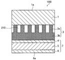
- FIG. 1 is a schematic view of a first embodiment of a light emitting device of the present invention.
- FIG. 2 is a schematic view of a second embodiment of the light emitting device of the present invention.
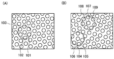
- FIG. 3 is an explanatory diagram of a method for calculating the degree of ordering of micropores.
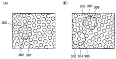
- FIG. 4 is an explanatory diagram of a method for calculating the degree of ordering of the columnar portions.
- FIG. 5 is a schematic end view of an aluminum substrate and an anodized film formed on the aluminum substrate.
- FIG. 6 is a partial cross-sectional view of an aluminum anodic oxide film which is a preferred example of a microstructure having micropores.
- FIG. 7 is a surface photograph (magnification of 10,000 times) of the aluminum anodic oxide film after the aluminum substrate was dissolved and removed in Example 1.
- FIG. 8 is a cross-sectional view schematically showing the manufacturing process of the light emitting device manufactured in Example 3.
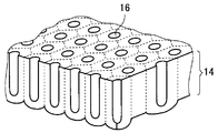
- FIG. 9 is an explanatory diagram for calculating the density of the columnar portions.
- 1st Embodiment of the light emitting element of this invention is a light emitting element which comprises a light emission part and a microstructure,
- the microstructure has a surface parallel to the light emitting surface of the light emitting element, and the surface parallel to the light emitting surface of the light emitting element has an average pore diameter of 5 to 1000 nm and an average pore density of 1 ⁇ 10 6. It is characterized in that micropores having a degree of ordering defined by the following formula (i) of 50% or more at ⁇ 1 ⁇ 10 10 pieces / mm 2 are formed.
- Ordering degree (%) B / A ⁇ 100 (i)
- A represents the total number of micropores in the measurement range.
- B is centered on the center of gravity of one micropore, and when a circle with the shortest radius inscribed in the edge of another micropore is drawn, the center of gravity of the micropores other than the one micropore is inside the circle. This represents the number in the measurement range of the one micropore to be included.
- the second embodiment of the light-emitting element of the present invention includes a light-emitting portion in which a first electrode, a light-emitting layer, and a second electrode are provided in this order, and a microstructure provided adjacent to the light-emitting portion.
- the fine structure has a plurality of columnar portions that stand in a substantially vertical direction with respect to the surface of the light emitting portion where the light emitting portion and the fine structure are in contact with each other,
- a light emitting device having an average maximum diameter of 5 to 1000 nm, a density of 1 ⁇ 10 6 to 1 ⁇ 10 10 pieces / mm 2 , and a degree of ordering defined by the formula (ii) of 50% or more. is there.
- Ordering degree (%) D / C ⁇ 100 (ii)
- C represents the total number of columnar portions in the measurement range.
- D is the center of gravity of one columnar part, and when a circle with the shortest radius inscribed in the edge of the other columnar part is drawn, the center of gravity of the columnar part other than the one columnar part is inside the circle.
- the number in the measurement range of the one columnar part to be included is represented.
- FIG. 1 is a schematic diagram of a first embodiment of a light emitting device of the present invention
- FIG. 2 is a schematic diagram of a second embodiment of the light emitting device of the present invention.
- the light emitting element 10A in FIG. 1 and the light emitting element 10B in FIG. 2 are shown as EL elements.
- the EL element referred to here includes a wide range of light emitting elements that emit light when an electric field is applied.
- injection type EL elements such as LED elements are used. Including.
- the substrate 1, the fine structures 2 and 3, and the light emitting unit 7. are provided in this order.
- the light-emitting portion 7 in FIGS. 1 and 2 is a typical light-emitting portion of an EL element in which a light-emitting layer 5 that emits light when an electric field is applied is sandwiched between a first electrode 4 and a second electrode 6. Structure.
- the fine structure 2 functions as a diffraction grating portion or a light scattering layer, a micropore 200 is formed on a surface 2a parallel to the light emitting surface 1a.
- the fine structure 3 functions as a diffraction grating part or a light scattering layer, so that at least the surface of the light emitting part 7 where the light emitting part 7 and the fine structure 3 are in contact with each other.
- a plurality of columnar portions 3a are formed in a substantially vertical direction.
- the microstructure 3 may have a film-like part 3b as shown in FIG. 2 from the viewpoint of facilitating the holding of the columnar part 3a.
- gap part 210 which exists between the some columnar parts 3a may remain a space
- the fine structure 2 functions as a transmission type diffraction grating portion or a transmission type light scattering layer.
- the emitted light passes through the fine structures 2 and 3 and the substrate 1 and is emitted to the outside. Therefore, the surface 1a of the upper substrate 1 in the drawing is a light emitting surface.
- the fine structures 2 and 3 function as a reflection type diffraction grating portion or a reflection type light scattering layer,
- the light emitted from the light emitting layer 5 is reflected by the fine structures 2 and 3, then passes through the light emitting unit 7 and is emitted to the outside. Therefore, the surface 6a of the second electrode 6 on the lower side in the figure becomes the light emitting surface.
- the light-emitting elements 10A and 10B shown in FIGS. 1 and 2 transmit the optical characteristics of the microstructures 2 and 3 to be used, that is, the light emitted from the light-emitting layer 5, or the light-emitting layer 5 Depending on whether the light emitted from the light source is reflected, it can be configured as either a bottom emission type light emitting element or a top emission type light emitting element.
- the light emitting elements 10A and 10B shown in FIGS. 1 and 2 have a structure in which the fine structures 2 and 3 and the light emitting portion 7 are sequentially stacked on the substrate 1.
- the present invention is not limited to this.
- 3 and the light emitting unit 7 may be included.
- Specific examples of such other components include protection that is optionally formed between the substrate 1 and the fine structures 2 and 3 and / or between the fine structures 2 and 3 and the light emitting portion 7. Examples thereof include a functional film such as a layer.
- the light emitting elements 10A and 10B shown in FIGS. 1 and 2 have a structure in which the fine structures 2 and 3 and the light emitting portion 7 are sequentially stacked on the substrate 1, but the essential components in the light emitting element of the present invention are It is a light emission part and a fine structure. Therefore, when the function as a light-emitting element can be exhibited without a substrate, the substrate may not be provided. In this case, the light emitting element has a structure in which the fine structures 2 and 3 and the light emitting portion 7 are laminated.
- the fine structures 2 and 3 function as a transmissive diffraction grating portion or a transmissive light scattering layer
- the light emitted from the light emitting layer 5 passes through the fine structures 2 and 3. Since the light is emitted to the outside, the surface exposed to the outside of the fine structures 2 and 3 on the side opposite to the light emitting portion 7 (the surface 2a on which the micropore 200 is formed or the uneven surface of the fine structure 3) is the light emitting element.
- the light emitting surface is the other hand.
- the fine structures 2 and 3 function as a reflection type diffraction grating part or a reflection type light scattering layer
- the light emitted from the light emitting layer 5 is emitted after being reflected by the fine structures 2 and 3. It passes through the part 7 and is discharged to the outside. Therefore, the surface 6a of the second electrode 6 on the lower side in the figure becomes the light emitting surface.
- the light emitting elements 10A and 10B shown in FIGS. 1 and 2 have a structure in which the fine structures 2 and 3 and the light emitting unit 7 are sequentially stacked on the substrate 1.
- the order is not limited to this.
- a structure in which a light emitting portion and a fine structure are sequentially stacked on a substrate may be used.
- the light emitting element having such a structure can also be configured as either a bottom emission type light emitting element or a top emission type light emitting element depending on the optical characteristics of the microstructure used.
- the fine structures 2 and 3 function as a transmissive diffraction grating portion or a transmissive light scattering layer, the light emitted from the light emitting layer is emitted to the outside through the fine structure.
- the surface exposed to the outside of the fine structure (the surface 2a on which the micropore 200 of the fine structure 2 is formed or the uneven surface of the fine structure 3) is the light emitting surface of the light emitting element.
- the fine structures 2 and 3 function as a reflection type diffraction grating part or a reflection type light scattering layer, the light emitted from the light emitting layer is reflected by the fine structure and then the light emitting part, and Since it is emitted to the outside through the substrate, it becomes a bottom emission type light emitting element.
- the surface exposed to the outside of the substrate becomes the light emitting surface of the light emitting element.
- the physical properties required for the substrate 1 differ depending on whether the light emitting elements 10A and 10B are bottom emission type light emitting elements or top emission type light emitting elements.
- the light emitted from the light emitting layer 5 passes through the fine structures 2 and 3 and the substrate 1 and is emitted to the outside. It is necessary to use a material that transmits light emitted from the light emitting layer 5.
- substrate 1 is not specifically limited as long as the intended translucency can be exhibited.
- the substrate 1 is not required to have translucency, so that the substrate 1 can be formed of any material.
- the substrate 1 of the top emission type light emitting element include a glass substrate, a plastic substrate, a semiconductor substrate, and the like.
- the thickness of the substrate 1 is not particularly limited.
- the light emitting unit 7 shown in FIGS. 1 and 2 is a light emitting unit of an EL element in which a light emitting layer 5 that emits light when an electric field is applied is sandwiched between a first electrode 4 and a second electrode 6.
- the EL element in this specification includes a wide range of light emitting elements that emit light by applying an electric field, and is an injection type such as an LED element in addition to an intrinsic EL element such as an organic EL element or an inorganic EL element. The EL element is also included.
- the light emitting layer 5 may be configured as a light emitting layer of an injection type EL element such as an LED element, or may be configured as a light emitting layer of an intrinsic EL element such as an organic EL element or an inorganic EL element.
- One of the first electrode 5 and the second electrode 7 is an anode, and the other is a cathode.
- the first electrode 4 provided on the light emitting surface 1 a side out of the first electrode 4 and the second electrode 6 emits light from the light emitting layer 5.
- the transmitted light needs to be transmitted.
- both the first electrode 5 and the second electrode 7 need to transmit light emitted from the light emitting layer 5.
- the thicknesses of the first electrode 5 and the second electrode 7 are not particularly limited as long as the original function as an electrode is expressed. For example, the thickness is within a range of 0.01 ⁇ m to 5 ⁇ m. Can do.
- the light-emitting elements of the present invention are not limited to EL elements, and may be light-emitting elements other than EL.
- the fine structure 2 having the micropore 200 or the fine structure 3 having the columnar part 3a functions as a light transmission type or light reflection type diffraction grating part or a light scattering layer. Therefore, it is preferable that the light-emitting element has scattered light that does not travel straight. Note that when a light-emitting element other than an EL element is used, the light-emitting portion has a structure corresponding to the light-emitting element.
- the configuration of each part will be described in more detail in the case where the light emitting element is a bottom emission type organic EL element.
- the substrate 1 is preferably a substrate that does not scatter or attenuate the light emitted from the light emitting layer 5.
- Specific examples thereof include zirconia stabilized yttrium (YSZ), inorganic materials such as glass, polyesters such as polyethylene terephthalate, polybutylene phthalate, and polyethylene naphthalate, polystyrene, polycarbonate, polyethersulfone, polyarylate, polyimide, and polycycloolefin. , Norbornene resins, and organic materials such as poly (chlorotrifluoroethylene).
- YSZ zirconia stabilized yttrium
- inorganic materials such as glass
- polyesters such as polyethylene terephthalate, polybutylene phthalate, and polyethylene naphthalate
- polystyrene polycarbonate
- polyethersulfone polyarylate
- polyimide polycycloolefin
- Norbornene resins Norbornene resins
- soda-lime glass it is preferable to use what gave barrier coatings, such as a silica.
- barrier coatings such as a silica.
- an organic material it is preferable that it is excellent in heat resistance, dimensional stability, solvent resistance, electrical insulation, and workability.
- the shape, structure, size and the like of the substrate 1 are not particularly limited and can be appropriately selected according to the use, purpose, etc. of the light emitting element (organic EL element).
- the shape of the substrate is preferably a plate shape.
- the structure of the substrate may be a single layer structure, a laminated structure, may be formed of a single member, or may be formed of two or more members.
- the substrate 1 may be colorless and transparent or colored and transparent, but is preferably colorless and transparent in that it does not scatter or attenuate the light emitted from the light emitting layer 5.
- the substrate 1 can be provided with a moisture permeation preventing layer (gas barrier layer) on the front surface or the back surface.
- a moisture permeation preventive layer gas barrier layer
- inorganic materials such as silicon nitride and silicon oxide are preferably used.
- the moisture permeation preventing layer (gas barrier layer) can be formed by, for example, a high frequency sputtering method.
- a substrate made of a thermoplastic material is used, a hard coat layer, an undercoat layer, or the like may be further provided as necessary.
- the anode usually has a function as an electrode for supplying holes to the light emitting layer 5, and there is no particular limitation on the shape, structure, size, etc., and the use of the light emitting element (organic EL element) Depending on the purpose, it can be appropriately selected from known electrode materials. As described above, in the case of the bottom emission type light emitting element, the first electrode 4 provided on the light emitting surface 1a side out of the first electrode 4 and the second electrode 6 is light emitted from the light emitting layer 5. However, the anode is usually provided as the transparent electrode.
- Suitable examples of the material for the anode include metals, alloys, metal oxides, conductive compounds, and mixtures thereof.
- Specific examples of the anode material include conductive metals such as tin oxide doped with antimony and fluorine (ATO, FTO), tin oxide, zinc oxide, indium oxide, indium tin oxide (ITO), and indium zinc oxide (IZO).
- Metals such as oxides, gold, silver, chromium, nickel, and mixtures or laminates of these metals and conductive metal oxides, inorganic conductive materials such as copper iodide and copper sulfide, polyaniline, polythiophene, polypyrrole, etc.
- conductive metal oxides are preferable, and ITO is particularly preferable from the viewpoints of productivity, high conductivity, transparency, and the like.
- the anode is composed of, for example, a wet method such as a printing method and a coating method, a physical method such as a vacuum deposition method, a sputtering method, and an ion plating method, and a chemical method such as a CVD and a plasma CVD method. It can be formed on the substrate in accordance with a method appropriately selected in consideration of suitability for the material to be used. For example, when ITO is selected as the anode material, the anode can be formed according to a direct current or high frequency sputtering method, a vacuum deposition method, an ion plating method, or the like.
- the position where the anode is formed is not particularly limited, and can be appropriately selected according to the use and purpose of the light emitting element (organic EL element). However, as described above, it is preferable to form the first electrode 4 provided on the light emitting surface 1a side as an anode.
- the anode may be formed so as to cover the entire surface of one side of the light emitting layer 5, or may be formed so as to cover a part of the surface.
- the patterning for forming the anode may be performed by chemical etching such as photolithography, or may be performed by physical etching such as laser, or vacuum deposition or sputtering with a mask overlapped. It may be performed by a lift-off method or a printing method.
- the thickness of the anode can be appropriately selected depending on the material constituting the anode and cannot be generally defined, but is usually about 10 nm to 50 ⁇ m, and preferably 50 nm to 20 ⁇ m.
- the resistance value of the anode is preferably 10 3 ⁇ / ⁇ or less, and more preferably 10 2 ⁇ / ⁇ or less.
- the anode is a transparent electrode, it may be colorless and transparent or colored and transparent.
- the transmittance of light emitted from the light emitting layer 5 is preferably 60% or more, and more preferably 70% or more.
- transparent anode is described in detail in the book “New Development of Transparent Electrode Film” published by CMC (1999), supervised by Yutaka Sawada, and the matters described here can be applied to the present invention.
- a transparent anode formed using ITO or IZO at a low temperature of 150 ° C. or lower is preferable.
- the cathode usually only needs to have a function as an electrode for injecting electrons into the light emitting layer 5, and there is no particular limitation on the shape, structure, size, etc. Depending on the purpose, it can be appropriately selected from known electrode materials.
- Examples of the material constituting the cathode include metals, alloys, metal oxides, electrically conductive compounds, and mixtures thereof. Specific examples include alkali metals (eg, LI, Na, K, Cs, etc.), alkaline earth metals (eg, Mg, Ca, etc.), gold, silver, lead, aluminum, sodium-potassium alloys, lithium-aluminum alloys, magnesium. -Rare earth metals such as silver alloys, indium and ytterbium. These may be used alone, but two or more can be suitably used in combination from the viewpoint of achieving both stability and electron injection.
- alkali metals eg, LI, Na, K, Cs, etc.
- alkaline earth metals eg, Mg, Ca, etc.
- gold silver, lead, aluminum, sodium-potassium alloys, lithium-aluminum alloys, magnesium.
- -Rare earth metals such as silver alloys, indium and ytterbium. These may be used alone,
- an alkali metal or an alkaline earth metal is preferable from the viewpoint of electron injecting property
- a material mainly composed of aluminum is preferable from the viewpoint of excellent storage stability.
- the material mainly composed of aluminum is aluminum alone, an alloy of aluminum and 0.01% by mass to 10% by mass of alkali metal or alkaline earth metal, or a mixture thereof (for example, lithium-aluminum alloy, Magnesium-aluminum alloy).
- the resistance value of the cathode is preferably 10 3 ⁇ / ⁇ or less, and more preferably 10 2 ⁇ / ⁇ or less.
- the method for forming the cathode is not particularly limited, and can be performed according to a known method.
- the cathode described above is configured from a wet method such as a printing method or a coating method, a physical method such as a vacuum deposition method, a sputtering method, or an ion plating method, or a chemical method such as CVD or plasma CVD method. It can be formed according to a method appropriately selected in consideration of suitability with the material. For example, when a metal or the like is selected as the cathode material, one or more of them can be simultaneously or sequentially performed according to a sputtering method or the like.
- Patterning when forming the cathode may be performed by chemical etching such as photolithography, physical etching by laser, or the like, or by vacuum deposition or sputtering with the mask overlaid. It may be performed by a lift-off method or a printing method.
- the cathode formation position there is no restriction
- the first electrode 4 provided on the light emitting surface 1a side is preferably formed as an anode as described above, the second electrode 6 is preferably formed as a cathode.
- the cathode may be formed so as to cover one whole surface of the light emitting layer 5 or may be formed so as to cover a part of the surface.
- a dielectric layer made of an alkali metal or alkaline earth metal fluoride, oxide or the like may be inserted between the cathode and the light emitting layer in a thickness of 0.1 nm to 5 nm.
- This dielectric layer can also be regarded as a kind of electron injection layer.
- the dielectric layer can be formed by, for example, a vacuum deposition method, a sputtering method, an ion plating method, or the like.
- the thickness of the cathode can be appropriately selected depending on the material constituting the cathode and cannot be generally defined, but is usually about 10 nm to 5 ⁇ m, and preferably 50 nm to 1 ⁇ m. Further, the cathode may be transparent or opaque.
- the transparent cathode can be formed by depositing a thin cathode material to a thickness of 1 nm to 10 nm and further laminating a transparent conductive material such as ITO or IZO.
- the light emitting layer 5 can have a structure in which one or more organic compound layers including an active layer are stacked.
- the active layer refers to a region where holes and electrons are combined, and emits light when the holes and electrons are combined in the region.
- the light emitting layer 5 may include a layer other than the active layer, and may include, for example, at least one of a hole transport layer and an electron transport layer in order to improve the coupling efficiency between holes and charges.
- the hole transport layer is inserted between the active layer and the anode
- the electron transport layer is inserted between the active layer and the cathode.
- the materials of the active layer, the hole transport layer, and the electron transport layer are not particularly limited, and any material can be used as long as it is an active layer material, a hole transport material, or an electron transport material usually used in an organic EL element. it can.
- stacked in order of the positive hole transport layer, the active layer, and the electron carrying layer from the anode side is preferable. Furthermore, a hole injection layer is provided between the hole transport layer and the anode, and / or an electron transport intermediate layer is provided between the active layer and the electron transport layer. Further, a hole transporting intermediate layer may be provided between the active layer and the hole transport layer, and similarly, an electron injection layer may be provided between the cathode and the electron transport layer. Each layer may be divided into a plurality of secondary layers.
- Each layer constituting the light emitting layer 5 can be suitably formed by any of dry film forming methods such as vapor deposition and sputtering, transfer methods, printing methods, coating methods, ink jet methods, and spray methods.
- dry film forming methods such as vapor deposition and sputtering, transfer methods, printing methods, coating methods, ink jet methods, and spray methods.
- the active layer may be composed of only a light emitting material, or may be configured as a mixed layer of a host material and a light emitting dopant.
- the luminescent dopant may be a fluorescent material or a phosphorescent material, and may be two or more kinds.
- the host material is preferably a charge transport material.
- the host material may be one type or two or more types, and examples thereof include a configuration in which an electron transporting host material and a hole transporting host material are mixed.
- the active layer may include a material that does not have charge transporting properties and does not emit light. Further, the active layer may be one layer or two or more layers, and each layer may emit light in different emission colors.
- any of phosphorescent luminescent materials and fluorescent luminescent materials can be used as the dopant.
- the active layer can contain two or more kinds of luminescent dopants in order to improve color purity and broaden the emission wavelength region.
- the light emitting dopant is a dopant satisfying the relationship of 1.2 eV> ⁇ Ip> 0.2 eV and / or 1.2 eV> ⁇ Ea> 0.2 eV with the host compound. It is preferable from the viewpoint.
- examples of the phosphorescent light-emitting dopant include complexes containing a transition metal atom or a lanthanoid atom.
- the transition metal atom is not particularly limited, but preferably includes ruthenium, rhodium, palladium, tungsten, rhenium, osmium, iridium, gold, silver, copper, and platinum, and more preferably rhenium, iridium. And platinum, more preferably iridium and platinum.
- lanthanoid atoms examples include lanthanum, cerium, praseodymium, neodymium, samarium, europium, gadolinium, terbium, dysprosium, holmium, erbium, thulium, ytterbium, and lutetium.
- neodymium, europium, and gadolinium are preferable.
- the specific ligand is preferably a halogen ligand (preferably a chlorine ligand) or an aromatic carbocyclic ligand (for example, preferably 5 to 30 carbon atoms, more preferably 6 to 6 carbon atoms). 30, more preferably 6 to 20 carbon atoms, particularly preferably 6 to 12 carbon atoms, such as cyclopentadienyl anion, benzene anion, or naphthyl anion), nitrogen-containing heterocyclic ligand (for example, preferably Has 5 to 30 carbon atoms, more preferably 6 to 30 carbon atoms, still more preferably 6 to 20 carbon atoms, particularly preferably 6 to 12 carbon atoms, and phenylpyridine, benzoquinoline, quinolinol, bipyridyl, or phenanthroline.
- a halogen ligand preferably a chlorine ligand
- aromatic carbocyclic ligand for example, preferably 5 to 30 carbon atoms, more preferably 6 to 6 carbon atom
- diketone ligand eg, acetylacetone, etc.
- carboxylic acid ligand eg, preferably 2-30 carbon atoms
- trimethylsilyloxy ligand dimethyl-tert-butylsilyloxy ligand, triphenylsilyloxy ligand, etc.
- carbon monoxide ligand isonitrile ligand, cyano ligand, phosphorus
- a ligand preferably having 3 to 40 carbon atoms, more preferably 3 to 30 carbon atoms, still more preferably 3 to 20 carbon atoms, particularly preferably 6 to 20 carbon atoms; Triphenylphosphine ligands), thiolato ligands (preferably having 1 to 30 carbon atoms, more preferably 1 to 20 carbon atoms, still more preferably 6 to 20 carbon atoms, such as phenylthiolato ligands) ),
- a phosphine oxide ligand preferably having 3 to 30 carbon atoms, more preferably 8 to 30 carbon atoms, still more preferably 18 to 30 carbon atoms, such as a triphenylphosphine oxide ligand. More
- the complex may have one transition metal atom in the compound or may be a so-called binuclear complex having two or more. Different metal atoms may be contained at the same time.
- phosphorescent luminescent dopant examples include, for example, US Pat. No. 6,303,238, US Pat. No. 6,097,147, International Publication No. 00/57676, International Publication No. 00/70655, International Publication. No. 01/08230 pamphlet, WO 01/39234 pamphlet, WO 01/41512 pamphlet, WO 02/02714 pamphlet, WO 02 / 15645A1, WO 02/44189 pamphlet, International Publication No. 05/19373, JP 2001-247859 A, JP 2002-302671 A, JP 2002-117978 A, JP 2003-133074 A, JP 2002-235076 A, Open 20 No. 3-123982, JP-A No.
- an Ir complex, a Pt complex, or a Re complex among which an Ir complex or a Pt complex containing at least one coordination mode of a metal-carbon bond, a metal-nitrogen bond, a metal-oxygen bond, and a metal-sulfur bond. Or a Re complex.
- an Ir complex, a Pt complex, or a Re complex containing a tridentate or higher polydentate ligand is particularly preferable.
- Fluorescent light-emitting dopants are generally benzoxazole, benzimidazole, benzothiazole, styrylbenzene, polyphenyl, diphenylbutadiene, tetraphenylbutadiene, naphthalimide, coumarin, pyran, perinone, oxadiazole, aldazine, pyralidine , Cyclopentadiene, bisstyrylanthracene, quinacridone, pyrrolopyridine, thiadiazolopyridine, cyclopentadiene, styrylamine, aromatic dimethylidin compounds, condensed polycyclic aromatic compounds (such as anthracene, phenanthroline, pyrene, perylene, rubrene, or pentacene) , 8-quinolinol metal complexes, various metal complexes represented by pyromethene complexes and rare
- the luminescent dopant in the active layer is generally contained in the active layer in an amount of 0.1% to 50% by mass based on the total mass of the compound forming the active layer. From the viewpoint of durability and external quantum efficiency. 1 to 50% by mass, and more preferably 2 to 40% by mass.
- the thickness of the active layer is not particularly limited, but it is usually preferably 2 nm to 500 nm. Among them, from the viewpoint of external quantum efficiency, it is more preferably 3 nm to 200 nm, and 5 nm to 100 nm. More preferably.
- a hole transporting host material having excellent hole transportability may be described as a hole transportable host
- an electron transporting host compound having excellent electron transportability in the case of being described as an electron transporting host
- ⁇ Hole-transporting host examples include the following materials. Pyrrole, indole, carbazole, azaindole, azacarbazole, triazole, oxazole, oxadiazole, pyrazole, imidazole, thiophene, polyarylalkane, pyrazoline, pyrazolone, phenylenediamine, arylamine, amino-substituted chalcone, styrylanthracene, fluorenone, hydrazone , Stilbene, silazane, aromatic tertiary amine compounds, styrylamine compounds, aromatic dimethylidin compounds, porphyrin compounds, polysilane compounds, poly (N-vinylcarbazole), aniline copolymers, thiophene oligomers, polythiophenes, etc.
- Conductive polymer oligomers organic silanes, carbon films, and derivatives thereof.
- Preferred are indole derivatives, carbazole derivatives, aromatic tertiary amine compounds, and thiophene derivatives, and more preferred are those having a carbazole group in the molecule.
- a compound having a t-butyl substituted carbazole group is preferable.
- the electron transporting host in the active layer preferably has an electron affinity Ea of 2.5 eV or more and 3.5 eV or less from the viewpoint of improving durability and reducing driving voltage, and is 2.6 eV or more and 3.4 eV or less. More preferably, it is 2.8 eV or more and 3.3 eV or less. Further, from the viewpoint of improving durability and reducing driving voltage, the ionization potential Ip is preferably 5.7 eV or more and 7.5 eV or less, more preferably 5.8 eV or more and 7.0 eV or less, and 5.9 eV or more. More preferably, it is 6.5 eV or less.
- Such an electron transporting host include the following materials. Pyridine, pyrimidine, triazine, imidazole, pyrazole, triazole, oxazole, oxadiazol, fluorenone, anthraquinodimethane, anthrone, diphenylquinone, thiopyran dioxide, carbodiimide, fluorenylidenemethane, distyrylpyrazine, Fluorine-substituted aromatic compounds, heterocyclic tetracarboxylic anhydrides such as naphthaleneperylene, phthalocyanines, and derivatives thereof (may form condensed rings with other rings), metal complexes and metals of 8-quinolinol derivatives Examples thereof include various metal complexes represented by metal complexes having phthalocyanine, benzoxazole or benzothiazol as a ligand.
- the electron transporting host include metal complexes, azole derivatives (benzimidazole derivatives, imidazopyridine derivatives, etc.), and azine derivatives (pyridine derivatives, pyrimidine derivatives, triazine derivatives, etc.).
- metal complexes are preferred.
- the metal complex is more preferably a metal complex having a ligand having at least one nitrogen atom, oxygen atom or sulfur atom coordinated to the metal.
- the metal ion in the metal complex is not particularly limited, but is preferably beryllium ion, magnesium ion, aluminum ion, gallium ion, zinc ion, indium ion, tin ion, platinum ion, or palladium ion, more preferably beryllium ion, Aluminum ion, gallium ion, zinc ion, platinum ion, or palladium ion, and more preferably aluminum ion, zinc ion, or palladium ion.
- the ligand is preferably a nitrogen-containing heterocyclic ligand (preferably having 1 to 30 carbon atoms, more preferably 2 to 20 carbon atoms, particularly preferably 3 to 15 carbon atoms). May be a bidentate or higher ligand, preferably a bidentate or higher and a hexadentate or lower ligand, and a bidentate or higher and lower 6 or lower ligand and a monodentate mixed ligand are also preferable. .
- the ligand examples include an azine ligand (for example, pyridine ligand, bipyridyl ligand, terpyridine ligand, etc.), a hydroxyphenylazole ligand (for example, hydroxyphenylbenzimidazole coordination). And a hydroxyphenylbenzoxazole ligand, a hydroxyphenylimidazole ligand, a hydroxyphenylimidazopyridine ligand, etc.), an alkoxy ligand (preferably having 1 to 30 carbon atoms, more preferably 1 carbon atom).
- azine ligand for example, pyridine ligand, bipyridyl ligand, terpyridine ligand, etc.
- a hydroxyphenylazole ligand for example, hydroxyphenylbenzimidazole coordination
- alkoxy ligand preferably having 1 to 30 carbon atoms, more preferably 1 carbon atom.
- aryloxy ligands preferably having 6 to 30 carbon atoms, more preferably 6 to 20 carbon atoms, particularly preferably 6 to 12 carbon atoms, for example phenyl And xyl, 1-naphthyloxy, 2-naphthyloxy, 2,4,6-trimethylphenyloxy, 4-biphenyloxy, etc.
- heteroaryloxy ligands preferably having 1 to 30 carbon atoms, more preferably Has 1 to 20 carbon atoms, particularly preferably 1 to 12 carbon atoms, and examples thereof include pyridyloxy, pyrazyloxy, pyrimidyloxy and quinolyloxy
- alkylthio ligands preferably 1 to 30 carbon atoms, more preferably Has 1 to 20 carbon atoms, particularly preferably 1 to 12 carbon atoms, and examples
- hetero A reelthio ligand preferably having 1 to 30 carbon atoms, more preferably 1 to 20 carbon atoms, particularly preferably 1 to 12 carbon atoms, such as pyridylthio, 2-benzimidazolylthio, 2-benzoxazolylthio, And 2-benzthiazolylthio
- siloxy ligands preferably having 1 to 30 carbon atoms, more preferably 3 to 25 carbon atoms, and particularly preferably 6 to 20 carbon atoms).
- Aromatic heterocyclic anion ligands preferably having 1 to 30 carbon atoms, more preferably 2 to 25 carbon atoms, particularly preferably 2 to 20 carbon atoms such as pyrrole anion, pyrazole anion, pyrazole anion, triazole anion, Examples thereof include an oxazole anion, a benzoxazole anion, a thiazole anion, a benzothiazole anion, a thiophene anion, and a benzothiophene anion.
- An indolenine anion ligand, etc. preferably a nitrogen-containing heterocyclic ligand, an aryloxy ligand, a heteroaryloxy group, or a siloxy ligand, more preferably a nitrogen-containing heterocyclic ring.
- Examples of the electron-transporting host that is a metal complex include, for example, Japanese Patent Application Laid-Open No. 2002-235076, Japanese Patent Application Laid-Open No. 2004-214179, Japanese Patent Application Laid-Open No. 2004-221106, Japanese Patent Application Laid-Open No. 2004-220165, and Japanese Patent Application Laid-Open No. And compounds described in JP-A No. 221068 and JP-A No. 2004-327313.
- the triplet lowest excitation level (T1) of the host material is preferably higher than T1 of the phosphorescent material in terms of color purity, luminous efficiency, and driving durability.
- the content of the host compound is not particularly limited, but may be 15% by mass or more and 95% by mass or less with respect to the total compound mass forming the active layer from the viewpoint of luminous efficiency and driving voltage. preferable.
- the hole injection layer and the hole transport layer are layers having a function of receiving holes from the anode or the anode side and transporting them to the cathode side.
- the hole injection material and the hole transport material used for these layers may be a low molecular compound or a high molecular compound.
- pyrrole derivatives carbazole derivatives, triazole derivatives, oxazole derivatives, oxadiazole derivatives, imidazole derivatives, polyarylalkane derivatives, pyrazoline derivatives, pyrazolone derivatives, phenylenediamine derivatives, arylamine derivatives, amino-substituted chalcone derivatives, styryl Anthracene derivatives, fluorenone derivatives, hydrazone derivatives, stilbene derivatives, silazane derivatives, aromatic tertiary amine compounds, styrylamine compounds, aromatic dimethylidin compounds, phthalocyanine compounds, porphyrin compounds, thiophene derivatives, organosilane derivatives, carbon, etc. It is preferable that it is a layer containing.
- An electron-accepting dopant can be contained in the hole injection layer or the hole transport layer of the organic EL element.
- an inorganic compound or an organic compound can be used as long as it has an electron-accepting property and oxidizes an organic compound.
- the inorganic compound include metal halides such as ferric chloride, aluminum chloride, gallium chloride, indium chloride, and antimony pentachloride, metal oxides such as vanadium pentoxide, and molybdenum trioxide.
- a compound having a nitro group, a halogen, a cyano group, a trifluoromethyl group or the like as a substituent a quinone compound, an acid anhydride compound, fullerene C60, or the like can be preferably used.
- the compounds described in JP-A-2003-229278, JP-A-2004-342614, JP-A-2005-72012, JP-A-2005-166637, JP-A-2005-209643 and the like are preferably used. Can be used.
- electron accepting dopants may be used alone or in combination of two or more.
- the amount of the electron-accepting dopant used varies depending on the type of material, but is preferably 0.01% by mass to 50% by mass with respect to the hole transport layer material, and is 0.05% by mass to 20% by mass. It is more preferable that the content be 0.1% by mass to 10% by mass.
- the thicknesses of the hole injection layer and the hole transport layer are each preferably 500 nm or less from the viewpoint of lowering the driving voltage.
- the thickness of the hole transport layer is preferably 1 nm to 500 nm, more preferably 5 nm to 200 nm, and even more preferably 10 nm to 100 nm.
- the thickness of the hole injection layer is preferably from 0.1 nm to 200 nm, more preferably from 0.5 nm to 100 nm, and even more preferably from 1 nm to 100 nm.
- the hole injection layer and the hole transport layer may have a single-layer structure composed of one or more of the materials described above, or may have a multilayer structure composed of a plurality of layers having the same composition or different compositions. .
- the electron injection layer and the electron transport layer are layers having a function of receiving electrons from the cathode or the cathode side and transporting them to the anode side.
- the electron injection material and the electron transport material used for these layers may be a low molecular compound or a high molecular compound.
- the electron injection layer or the electron transport layer of the organic EL element can contain an electron donating dopant.
- the electron donating dopant introduced into the electron injecting layer or the electron transporting layer only needs to have an electron donating property and a property of reducing an organic compound, such as an alkali metal such as Li or an alkaline earth metal such as Mg. Transition metals including rare earth metals and reducing organic compounds are preferably used.
- a metal having a work function of 4.2 eV or less can be preferably used. Specifically, Li, Na, K, Be, Mg, Ca, Sr, Ba, Y, Cs, La, Sm, Gd , And Yb.
- Examples of the reducing organic compound include nitrogen-containing compounds, sulfur-containing compounds, and phosphorus-containing compounds.
- the methods described in JP-A-6-212153, JP-A-2000-196140, JP-A-2003-68468, JP-A-2003-229278, JP-A-2004-342614, etc. Materials can be used.
- electron donating dopants may be used alone or in combination of two or more.
- the amount of the electron-donating dopant used varies depending on the type of material, but is preferably 0.1% by mass to 99% by mass, and 1.0% by mass to 80% by mass with respect to the electron transport layer material. Is more preferable, and 2.0 mass% to 70 mass% is particularly preferable.
- the thicknesses of the electron injection layer and the electron transport layer are each preferably 500 nm or less from the viewpoint of lowering the driving voltage.
- the thickness of the electron transport layer is preferably 1 nm to 500 nm, more preferably 5 nm to 200 nm, and even more preferably 10 nm to 100 nm.
- the thickness of the electron injection layer is preferably from 0.1 nm to 200 nm, more preferably from 0.2 nm to 100 nm, and even more preferably from 0.5 nm to 50 nm.
- the electron injection layer and the electron transport layer may have a single layer structure composed of one or more of the above-described materials, or may have a multilayer structure composed of a plurality of layers having the same composition or different compositions.
- the hole blocking layer is a layer having a function of preventing holes transported from the anode side to the active layer from passing through to the cathode side.
- a hole blocking layer can be provided as an organic compound layer adjacent to the active layer on the cathode side.
- Examples of the compound constituting the hole blocking layer include aluminum complexes such as BAlq, triazole derivatives, phenanthroline derivatives such as BCP, and the like.
- the thickness of the hole blocking layer is preferably 1 nm to 500 nm, more preferably 5 nm to 200 nm, and even more preferably 10 nm to 100 nm.
- the hole blocking layer may have a single layer structure composed of one or more of the above-described materials, or may have a multilayer structure composed of a plurality of layers having the same composition or different compositions.
- the electron blocking layer is a layer having a function of preventing electrons transported from the cathode side to the active layer from passing through to the anode side.
- An electron block layer can be provided as an organic compound layer adjacent to the active layer on the anode side.
- the compound constituting the electron blocking layer for example, those mentioned as the hole transport material described above can be applied.
- the thickness of the electron blocking layer is preferably 1 nm to 500 nm, more preferably 5 nm to 200 nm, and even more preferably 10 nm to 100 nm.
- the hole blocking layer may have a single layer structure composed of one or more of the above-described materials, or may have a multilayer structure composed of a plurality of layers having the same composition or different compositions.
- a charge generation layer may be provided between a plurality of active layers.
- the charge generation layer is a layer having a function of generating charges (holes and electrons) when an electric field is applied and a function of injecting the generated charges into a layer adjacent to the charge generation layer.
- the material for forming the charge generation layer may be any material having the above-described function, and may be formed of a single compound or a plurality of compounds. Specifically, it may be a conductive material, a semiconductive material such as a doped organic layer, or an electrically insulating material. Examples thereof include materials described in JP-A-11-329748, JP-A 2003-272860, and JP-A 2004-39617.
- transparent conductive materials such as ITO and IZO (indium zinc oxide), fullerenes such as C60, conductive organic materials such as oligothiophene, metal phthalocyanines, metal-free phthalocyanines, metal porphyrins, metal-free Conductive organic materials such as porphyrins, metal materials such as Ca, Ag, Al, Mg: Ag alloy, Al: Li alloy, Mg: Li alloy, hole conductive material, electron conductive material, and a mixture thereof May be used.
- ITO and IZO indium zinc oxide
- fullerenes such as C60
- conductive organic materials such as oligothiophene
- metal phthalocyanines metal-free phthalocyanines
- metal porphyrins metal-free Conductive organic materials such as porphyrins
- metal materials such as Ca, Ag, Al, Mg: Ag alloy, Al: Li alloy, Mg: Li alloy, hole conductive material, electron conductive material, and a mixture thereof May be used.
- the hole conductive material examples include a material in which a hole transporting organic material such as 2-TNATA or NPD is doped with an oxidizing agent having an electron withdrawing property such as F4-TCNQ, TCNQ, or FeCl 3 , or a P-type conductive material.
- the electron conductive material includes an electron transporting organic material doped with a metal or a metal compound having a work function of less than 4.0 eV, an N type conductive polymer, N type Type semiconductors.
- the N-type semiconductor include N-type Si, N-type CdS, and N-type ZnS.
- the P-type semiconductor examples include P-type Si, P-type CdTe, and P-type CuO.
- An electric insulating material such as V 2 O 5 can also be used for the charge generation layer.
- the charge generation layer may be a single layer or a plurality of layers.
- a structure in which a plurality of layers are stacked includes a conductive material such as a transparent conductive material and a metal material and a hole conductive material, or a structure in which an electron conductive material is stacked, and the above hole conductive material and electron conductive And a layer having a structure in which a functional material is laminated.
- the film thickness is not particularly limited, but is preferably 0.5 nm to 200 nm, more preferably 1 nm to 100 nm, still more preferably 3 nm to 50 nm, and particularly preferably 5 nm to 30 nm.
- the method for forming the charge generation layer is not particularly limited, and the method for forming the organic compound layer such as the active layer described above can be used.
- the charge generation layer is formed between two or more active layers, but the anode side and the cathode side of the charge generation layer may contain a material having a function of injecting charges into adjacent layers.
- an electron injection compound such as BaO, SrO, Li 2 O, LiCl, LiF, MgF 2 , MgO, or CaF 2 is used as the anode of the charge generation layer. It may be laminated on the side.
- the material of the generation layer can be selected.
- the organic EL device can obtain light emission by applying a direct current (which may include an alternating current component if necessary) voltage (usually 2 to 15 volts) or a direct current between the anode and the cathode.
- a direct current which may include an alternating current component if necessary
- a direct current usually 2 to 15 volts
- a direct current usually 2 to 15 volts
- the microstructure 2 has a light emitting surface of a light emitting element (1a when the light emitting element 10A shown in FIG. 1 is a bottom emission type light emitting element, and 6a when the light emitting element 10A shown in FIG. 1 is a top emission type light emitting element).
- a micropore 200 is formed on the surface 2a parallel to the light emitting surface of the light emitting element.
- the average pore diameter of the micropores 200 on the surface 2a is 5 to 1000 nm
- the average pore density of the micropores 200 on the surface 2a is 1 ⁇ 10 6 to 1 ⁇ 10 10 holes / mm 2 .
- the degree of ordering defined by the following formula (i) is 50% or more.
- Ordering degree (%) B / A ⁇ 100 (i)
- A represents the total number of micropores in the measurement range.
- B is centered on the center of gravity of one micropore, and when a circle with the shortest radius inscribed in the edge of another micropore is drawn, the center of gravity of the micropore other than the one micropore is placed inside the circle. This represents the number in the measurement range of one micropore that will contain six.
- FIG. 3 is an explanatory diagram of a method for calculating the degree of ordering of micropores.
- the above formula (i) will be described more specifically with reference to FIG.
- the micropore 101 shown in FIG. 3A is drawn with a circle 103 (inscribed in the micropore 102) having the shortest radius centered on the center of gravity of the micropore 101 and inscribed in the edge of another micropore.
- the center of the micropores other than the micropores 101 is included in the circle 103. Therefore, the micropore 101 is included in B.
- the micropore 104 shown in FIG. 3B draws a circle 106 having the shortest radius (inscribed in the micropore 105) that is centered on the center of gravity of the micropore 104 and inscribed in the edge of another micropore.
- the center of gravity of the micropores other than the micropores 104 is included inside the circle 106. Therefore, the micropore 104 is not included in B.
- the micropore 107 shown in FIG. 3B is centered on the center of gravity of the micropore 107 and has the shortest radius 109 inscribed in the edge of the other micropore (inscribed in the micropore 108). Is drawn, the circle 109 includes seven centroids of micropores other than the micropore 107. Therefore, the micropore 107 is not included in B.
- the micropores 200 satisfying the above average pore diameter, average pore density, and degree of ordering are formed on the surface 2a parallel to the light emitting surface (1a or 6a) of the light emitting element 10A. It functions as a light transmission type or light reflection type diffraction grating part or a light scattering layer for the light emitted from the light emitting layer 5. Thereby, the extraction efficiency of the light emitted from the light emitting layer 5 is improved.
- the fine structure 2 functioning as a diffraction grating portion or a light scattering layer is formed with densely arranged micropores, and therefore has excellent uniformity of luminance in the direction of the light emitting surface, and luminance in the direction of the light emitting surface. There will be no shading.
- the average pore diameter of the micropore 200 is preferably 10 to 800 nm, and more preferably 15 to 500 nm. Similarly, the average pore density of the micropore 200 is preferably 5 ⁇ 10 6 to 5 ⁇ 10 9 pieces / mm 2 , and more preferably 1 ⁇ 10 7 to 1 ⁇ 10 9 pieces / mm 2. preferable. Similarly, the degree of ordering of the micropore 200 is preferably 60% or more, and more preferably 70% or more.
- the period of unevenness of the diffraction grating part which is defined as the distance between adjacent central points of the micropores, satisfies the following.
- the guided light inside the light emitting element includes the width of the waveguide layer (the fine structure 2 in the case of the light emitting element 10A shown in FIG. 1) and the adjacent cladding layer (in the case of the light emitting element 10A shown in FIG. 1), the first electrode 4. ) And parameters such as the refractive index of the waveguide layer and the guided light wavelength.
- the waveguide wavelength in vacuum is ⁇
- the refractive index of the waveguide layer is n
- the reflection angle of the m-th order guided light is ⁇ m
- the concave / convex period of the diffraction grating part is ⁇
- v is an integer
- the concave / convex period ⁇ is When expressed by the formula (iii), the guided light is diffracted in the direction perpendicular to the light emitting surface.
- ⁇ v ⁇ ⁇ / n ⁇ sin ⁇ m (iii)
- a diffraction grating having irregularities formed with a period satisfying the relationship represented by the above formula (iii) (in the case of the present invention, the distance between adjacent central points is set so as to satisfy the relationship represented by the above formula (iii).
- the fine structure in which the pores are formed can diffract light that has been guided inside the light emitting element in the direction perpendicular to the light emitting surface, and the diffracted light is emitted to the outside. become.
- the value of v is ⁇ 1
- the ⁇ 1st order diffracted light is preferably generated in the vertical direction. This is because the ⁇ 1st order diffraction efficiency is larger than the diffraction efficiency of other orders, and the increase rate of the light extraction efficiency becomes the most remarkable.
- the thickness of the fine structure 2 is preferably 0.05 ⁇ m to 150 ⁇ m, more preferably 0.10 to 100 ⁇ m, and particularly preferably 0.20 to 50 ⁇ m.
- the thickness of the fine structure 2 is more than 150 ⁇ m, it is not preferable because the light transmission itself is lowered when functioning as a transmission type diffraction grating portion or a transmission type light scattering layer.
- the thickness of the fine structure 2 is less than 0.05 ⁇ m, the strength of the fine structure is impaired.
- the microstructure 2 is not particularly limited as long as it has micropores 200 satisfying the above average pore diameter, average pore density, and degree of ordering on its surface, but the metal surface is made of an oxide of the metal by anodic oxidation.
- Anodized film obtained by anodizing a valve metal-derived material having the characteristics covered with the film, more specifically, by subjecting the valve metal or its alloy substrate to anodization The obtained anodic oxide film is preferable for forming a microstructure having on its surface micropores satisfying the above average pore diameter, average pore density, and degree of ordering.
- Specific examples of the valve metal include aluminum, tantalum, niobium, titanium, hafnium, zirconium, zinc, tungsten, bismuth, and antimony.
- the regularity of the micropores formed on the surface of the anodized film more specifically, the regularity of the pore arrangement of the micropores is excellent.
- the resulting aluminum anodized film is preferred.
- the aluminum anodic oxide film is a transparent film, and the obtained fine structure functions as a transmissive diffraction grating portion or a transmissive light scattering layer.
- the fine structure 3 has a plurality of columnar portions 3a that are erected in a direction substantially perpendicular to the surface of the light emitting portion where the light emitting portion and the fine structure are in contact. As described above, the fine structure 3 holds the columnar portions 3a. From the viewpoint of ease, the film-like portion 3b may be provided. Further, the fine structure 3 has a flat surface (the upper surface of the columnar portion 3a and the interface with the light emitting portion), the light emitting surface of the light emitting element (1a when the light emitting element 10B shown in FIG. 2 is a bottom emission type light emitting element, When the light emitting element 10B shown in FIG. 2 is a top emission type light emitting element, it is provided so as to be substantially parallel to 6a).
- the angle at which the columnar portion 3a stands is substantially perpendicular to the surface of the light emitting portion where the light emitting portion and the fine structure are in contact.
- the substantially vertical direction is preferably about 90 ° ⁇ 5 ° from the viewpoint of light extraction efficiency.
- the columnar portion 3a has an average maximum diameter of 5 to 1000 nm, a density of 1 ⁇ 10 6 to 1 ⁇ 10 10 pieces / mm 2 , and a regularization defined by the following formula (ii):
- the degree is provided to be 50% or more.
- Ordering degree (%) D / C ⁇ 100 (ii)
- C represents the total number of columnar portions in the measurement range.
- D is the center of gravity of one columnar part, and when a circle with the shortest radius inscribed in the edge of the other columnar part is drawn, the center of gravity of the columnar part other than the one columnar part is inside the circle.
- the number in the measurement range of the one columnar part to be included is represented.
- FIG. 4 is an explanatory diagram of a method of calculating the degree of ordering of the columnar portions.
- the above formula (ii) will be described more specifically with reference to FIG.
- a columnar portion 301 shown in FIG. 4A draws a circle 303 (inscribed in the columnar portion 302) having the shortest radius that is centered on the center of gravity of the columnar portion 301 and inscribed in an edge of another columnar portion.
- the center of gravity of the columnar parts other than the columnar part 301 is included inside the circle 303. Therefore, the columnar portion 301 is included in D.
- a columnar portion 307 shown in FIG. 4B is centered on the center of gravity of the columnar portion 307 and has the shortest radius 309 inscribed in the edge of the other columnar portion (inscribed in the columnar portion 308). Is drawn, the center of gravity of the columnar parts other than the columnar part 307 is included inside the circle 309. Therefore, the columnar portion 307 is not included in D.
- the microstructure 3 has a columnar portion 3a that satisfies the above average maximum diameter, density, and degree of ordering, so that a light transmission type or light reflection type diffraction grating for light emitted from the light emitting layer 5 is formed. Function as a light scattering layer. Thereby, the extraction efficiency of the light emitted from the light emitting layer 5 is improved.
- the fine structure 3 functioning as a diffraction grating portion or a light scattering layer is formed with dense regular columnar portions, and therefore has excellent uniformity in luminance in the direction of the light emitting surface, and luminance in the direction of the light emitting surface. There will be no shading.
- the average maximum diameter of the columnar part is preferably 10 to 800 nm, and preferably 15 to 500 nm. Is more preferable.
- the density of the columnar portions is preferably 5 ⁇ 10 6 to 5 ⁇ 10 9 pieces / mm 2 , and more preferably 1 ⁇ 10 7 to 1 ⁇ 10 9 pieces / mm 2 .
- the degree of ordering of the columnar part is preferably 70% or more.
- the period of the unevenness of the diffraction grating portion which is defined as the distance between adjacent center points of the columnar portions, is related to the fine structure 2 having the micropore 200. It is preferable to satisfy the same conditions as described for the period of the unevenness of the diffraction grating portion defined as the distance between adjacent center points.
- the preferable range of the thickness of the fine structure 3 is the same as that described for the preferable range of the thickness of the fine structure 2 having the micropores 200.
- the material of the microstructure 3 is not particularly limited as long as it has a columnar portion that satisfies the above-described average diameter, density, and degree of ordering.
- the first electrode 4 and the same material specifically, tin oxide doped with antimony or fluorine (ATO, FTO), tin oxide, zinc oxide, indium oxide, indium tin oxide (ITO), indium zinc oxide ( Conductive metal oxides such as IZO); metals such as gold, silver, chromium and nickel; mixtures or laminates of the above conductive metal oxides and the above metals; inorganic conductive materials such as copper iodide and copper sulfide; And organic conductive materials such as polyaniline, polythiophene, and polypyrrole.
- a conductive metal oxide is preferable, and ITO is particularly preferable from the viewpoints of productivity, high conductivity, transparency, and the like.
- the manufacturing method of the fine structure 3 is not particularly limited, from the viewpoint of forming the columnar part in the nano order, a method of transferring the shape using a material in which holes are similarly arranged in a lattice form in the nano order as a template is preferable.
- template it is more preferable to use the anodic oxide film which has the micropore formed by anodizing an aluminum base material from a viewpoint which can produce a nano-order hole simply.
- the method include a filling process in which a material for forming the fine structure is filled in the penetrated holes, and a removal process in which the anodic oxide film is removed after the filling process.
- the gaps 210 existing between the plurality of columnar parts 3a may remain as gaps or may be filled with a gap filling medium.
- the gap filling medium is not particularly limited as long as it has transparency and has a refractive index different from that of the fine structure 3.
- a medium having a refractive index difference from the fine structure 3 of 0.10 or more is preferable.
- the fine structure 3 is made of ITO (refractive index: 2.12), zinc oxide is used. (Refractive index: 1.98).
- the gap portion 210 by filling the gap portion 210 with a fluorescent dye that emits fluorescence upon receiving light from the light emitting portion 7, it is possible to absorb ultraviolet light from the light emitting portion 7 and improve the light emission amount in the visible light region.
- the fluorescent dye filled in the gap portion 210 the description about the mixing of the fluorescent dye into the microstructure 2 described later can be referred to.
- anodized aluminum film As described above, it is preferable to use an anodized film having micropores formed by anodizing an aluminum base material for the microstructure 2 having the micropores 200. Moreover, it is preferable to use an anodic oxide film having micropores formed by anodizing an aluminum base material as a template for forming the columnar portion 3a when the microstructure 3 is manufactured.
- preparation of an aluminum anodic oxide film suitable for manufacturing the fine structure 2 and the fine structure 3 will be described.
- the aluminum substrate is not particularly limited, and specific examples thereof include a pure aluminum material; an alloy material containing aluminum as a main component and containing a trace amount of foreign elements; and depositing high-purity aluminum on low-purity aluminum (for example, recycled material).
- Examples thereof include: a substrate obtained by coating a surface of silicon wafer, quartz, glass or the like with a high purity aluminum by a method such as vapor deposition or sputtering; a resin substrate obtained by laminating aluminum;
- the shape of the aluminum substrate is not particularly limited, and may be a block shape or an irregular shape material, but is preferably a plate material from the viewpoint of dissolution or peeling after anodization. In the following description, a case where an aluminum substrate is used will be described.
- the surface on which the anodizing treatment is performed preferably has a higher aluminum purity.
- the aluminum purity is preferably 99.5% by mass or more, more preferably 99.9% by mass or more, and further preferably 99.99% by mass or more.
- the regularity of the pore arrangement of the micropores formed on the surface of the aluminum anodic oxide film formed by anodizing becomes sufficient, and the aluminum anodic oxide film is microporous.
- the microstructure 2 is used as the microstructure 2 having 200, more specifically, when the microstructure 2 is used as a transmissive diffraction grating portion or a transmissive light scattering layer of the light emitting element, the light emission It is preferable from the viewpoint of improving the luminance uniformity of the element.
- the microstructure 3 manufactured using the aluminum anodic oxide film as a mold for forming the columnar portion 3a is used as a transmissive diffraction grating portion of a light emitting element or a transmissive light scattering layer, This is preferable from the viewpoint of improving luminance uniformity of the light emitting element.
- the surface to be anodized is preferably subjected to a degreasing process and a mirror finishing process in advance, and in particular, from the viewpoint of improving the regularity of the pore arrangement. Therefore, heat treatment is preferably performed.
- Heat treatment When heat treatment is performed, it is preferably performed at 200 to 350 ° C. for about 30 seconds to 2 minutes. Specifically, for example, a method of placing an aluminum substrate in a heating oven can be used. By performing such heat treatment, the regularity of the arrangement of micropores formed on the surface of the anodized film is improved. Moreover, it is preferable to cool the aluminum substrate after heat treatment rapidly. As a method for cooling, for example, a method of directly putting it into water or the like can be mentioned.
- the degreasing treatment uses acid, alkali, organic solvent, etc. to dissolve and remove the organic components such as dust, fat, and resin adhered to the surface of the aluminum substrate, and in each treatment described later due to the organic components. This is done for the purpose of preventing the occurrence of defects.
- the degreasing treatment for example, a method in which an organic solvent such as various alcohols (for example, methanol), various ketones (for example, methyl ethyl ketone), benzine, volatile oil or the like is brought into contact with the aluminum substrate surface at room temperature (organic Solvent method); a method of bringing a solution containing a surfactant such as soap or neutral detergent into contact with the aluminum substrate surface at a temperature from room temperature to 80 ° C., and then washing with water (surfactant method); concentration of 10 to 200 g / L sulfuric acid aqueous solution is brought into contact with the aluminum substrate surface at a temperature from room temperature to 70 ° C.
- organic Solvent method a method in which an organic solvent such as various alcohols (for example, methanol), various ketones (for example, methyl ethyl ketone), benzine, volatile oil or the like is brought into contact with the aluminum substrate surface at room temperature
- organic Solvent method a method of bringing a solution containing
- a sodium hydroxide aqueous solution having a concentration of 5 to 20 g / L is applied to the aluminum substrate surface at room temperature at 30 ° C. while contacted about seconds, the aluminum substrate surface and the electrolyte by passing a direct current of a current density of 1 ⁇ 10A / dm 2 in the cathode, the ,
- a method in which a nitric acid aqueous solution having a concentration of 100 to 500 g / L is brought into contact and neutralized; various known anodizing electrolytes are brought into contact with the surface of the metal substrate at room temperature, and the aluminum substrate surface is used as a cathode, and a current density of 1 to
- a direct current of 10 A / dm 2 is applied or an alternating current is applied for electrolysis; an aqueous alkali solution having a concentration of 10 to 200 g / L is contacted with the aluminum substrate surface at 40 to 50 ° C.
- the organic solvent method, the surfactant method, the emulsion degreasing method, and the phosphate method are preferable from the viewpoint that the fat on the surface of the aluminum substrate can be removed, but the dissolution of aluminum hardly occurs.
- a conventionally known degreasing agent can be used for the degreasing treatment.
- various commercially available degreasing agents can be used by a predetermined method.
- the mirror finishing process is performed in order to eliminate unevenness on the surface of the aluminum substrate, for example, rolling streaks generated during the rolling of the aluminum substrate, and improve the uniformity and reproducibility of the sealing process by an electrodeposition method or the like.
- the mirror finishing process is not particularly limited, and a conventionally known method can be used. Examples thereof include mechanical polishing, chemical polishing, and electrolytic polishing.
- Examples of mechanical polishing include a method of polishing with various commercially available polishing cloths, a method of combining various commercially available abrasives (for example, diamond, alumina) and buffs, and the like.
- abrasive for example, diamond, alumina
- buffs and the like.
- the final polishing agent is preferably # 1500.
- the glossiness can be 50% or more (in the case of rolled aluminum, both the rolling direction and the width direction are 50% or more).
- the gloss can be 70% or more (in the case of rolled aluminum, both the rolling direction and the width direction are 70% or more).
- a surface having an average surface roughness R a of 0.1 ⁇ m or less and a glossiness of 50% or more can be obtained.
- the average surface roughness Ra is preferably 0.03 ⁇ m or less, and more preferably 0.02 ⁇ m or less.
- the glossiness is preferably 70% or more, and more preferably 80% or more.
- the glossiness is a regular reflectance determined in accordance with JIS Z8741-1997 “Method 3 60 ° Specular Gloss” in the direction perpendicular to the rolling direction.
- variable angle gloss meter for example, VG-1D, manufactured by Nippon Denshoku Industries Co., Ltd.
- the incident reflection angle is 60 degrees and the regular reflectance is 70%.
- the incident / reflection angle is 20 degrees.
- the anodizing treatment is a treatment for forming an anodized film having micropores on the surface of the aluminum substrate by anodizing the aluminum substrate.
- a conventionally known method can be used as the anodizing treatment.
- a self-regulation described later is used. It is preferable to use a method using a conversion method or imprint processing.
- the self-ordering method is a method for improving the regularity by utilizing the property that the micropores formed in the anodic oxide film are regularly arranged and removing the factors that disturb the regular arrangement.
- a high-purity aluminum substrate is used, and an anodized film is formed at a low speed over a long period of time (for example, several hours to several tens of hours) at a voltage according to the type of the electrolytic solution.
- a desired pore diameter can be obtained to some extent by controlling the voltage.
- an anodic oxidation process (A) described later may be performed, but an anodic oxidation process (A), a film removal process (B), and a re-anodizing process (C) described later.
- an anodic oxidation process (A), a film removal process (B), and a re-anodizing process (C) described later In this order (self-ordering method I), a method in which an anodic oxidation process (D) and an oxide film dissolution process (E) described later are performed at least once in this order (self-ordering method II), etc. It is preferable to do this.
- each process of the self-ordering method I and the self-ordering method II which are preferred embodiments, will be described in detail.
- the average flow rate of the electrolytic solution in the anodizing treatment (A) is preferably 0.5 to 20.0 m / min, more preferably 1.0 to 15.0 m / min, and 2.0 to 10 More preferably, it is 0.0 m / min.
- anodization (A) at a flow rate in the above range, micropores having uniform and high regularity can be formed.
- the method of flowing the electrolytic solution under the above-mentioned conditions is not particularly limited, but, for example, a method using a general stirring device such as a stirrer is used.
- stirrer that can control the stirring speed with a digital display because the average flow rate can be controlled.
- examples of such a stirring apparatus include “Magnetic Stirrer HS-50D (manufactured by AS ONE)” and the like.
- anodizing treatment (A) for example, a method in which an aluminum substrate is used as an anode in a solution having an acid concentration of 0.1 to 20% by mass, preferably 1 to 10% by mass, can be used.
- the solution used for the anodizing treatment (A) is preferably an acid solution, and sulfuric acid, phosphoric acid, chromic acid, oxalic acid, sulfamic acid, benzenesulfonic acid, amidosulfonic acid, glycolic acid, tartaric acid, malic acid Citric acid and the like are more preferable, and sulfuric acid, phosphoric acid, and oxalic acid are particularly preferable. These acids can be used alone or in combination of two or more.
- the conditions of the anodizing treatment (A) vary depending on the electrolyte used, and therefore cannot be determined unconditionally. In general, however, the electrolyte concentration is 0.1 to 20% by mass, and the solution temperature is ⁇ 10 to 30 ° C.
- the current density is preferably 0.01 to 20 A / dm 2 , the voltage is 3 to 300 V, the electrolysis time is 0.5 to 30 hours, the electrolyte concentration is 0.5 to 15% by mass, the solution temperature is ⁇ 5 to 25 ° C.
- the current density is 0.05 to 15 A / dm 2
- the voltage is 5 to 250 V
- the electrolysis time is 1 to 25 hours
- the electrolyte concentration is 1 to 10% by mass
- the solution temperature is 0 to 20 ° C.
- the current density is 0.1. More preferably, it is ⁇ 10 A / dm 2
- voltage is 10 to 200 V
- electrolysis time is 2 to 20 hours.
- the treatment time for the anodizing treatment (A) is preferably 0.5 minutes to 16 hours, more preferably 1 minute to 12 hours, and even more preferably 2 minutes to 8 hours.
- the anodizing treatment (A) can be performed by changing the voltage intermittently or continuously in addition to being performed under a constant voltage. In this case, it is preferable to decrease the voltage sequentially. This makes it possible to reduce the resistance of the anodized film, and fine micropores are generated in the anodized film, which is preferable in terms of improving uniformity, particularly when sealing treatment is performed by electrodeposition. .
- the film thickness of the anodized film formed by such anodizing treatment (A) is preferably 1 to 300 ⁇ m, more preferably 5 to 150 ⁇ m, and still more preferably 10 to 100 ⁇ m.
- the average pore diameter of the micropores formed by such anodizing treatment (A) is preferably 5 to 1000 nm, and more preferably 10 to 250 nm.
- the opening diameter of the micropore is referred to as “pore diameter”.
- the micropores formed by such anodizing treatment (A) preferably have a pore diameter dispersion within 3% of the average pore diameter within a range of 1 ⁇ m 2. Is more preferable.
- the average pore diameter and the dispersion of the pore diameter can be obtained by the following equations, respectively.
- Xi is one pore diameter measured in the range of 1 ⁇ m 2 .
- the average pore density of micropores in the anodized film formed by such anodizing treatment (A) is preferably 200 / ⁇ m 2 or more.
- the area ratio occupied by the micropores is preferably 3 to 50%.
- the area ratio occupied by the micropores is defined by the ratio of the total area of the opening portions of the micropores to the area of the surface of the aluminum anodized film.
- the film removal process (B) is a process for dissolving and removing the anodized film formed on the surface of the aluminum substrate by the anodizing process (A). After forming the anodized film on the surface of the aluminum substrate by the anodizing process (A), a penetration process step described later may be performed immediately. However, after the anodizing process (A), the film removal process (B ) And re-anodizing treatment (C) described later are preferably performed in this order.
- the bottom part of the anodized film remaining on the surface of the aluminum substrate is removed once by this film removal treatment (B). Can be exposed to the surface to obtain regular depressions. Therefore, in the film removal process (B), the aluminum substrate is not dissolved, but only the anodized film made of alumina (aluminum oxide) is dissolved.
- Alumina solution includes chromium compound, nitric acid, phosphoric acid, zirconium compound, titanium compound, lithium salt, cerium salt, magnesium salt, sodium fluorosilicate, zinc fluoride, manganese compound, molybdenum compound, magnesium compound, barium compound and An aqueous solution containing at least one selected from the group consisting of simple halogens is preferred.
- the chromium compound include chromium (III) oxide and anhydrous chromium (VI) acid.
- zirconium-based compound include zircon ammonium fluoride, zirconium fluoride, and zirconium chloride.
- titanium compound include titanium oxide and titanium sulfide.
- the lithium salt include lithium fluoride and lithium chloride.
- the cerium salt include cerium fluoride and cerium chloride.
- the magnesium salt include magnesium sulfide.
- the manganese compound include sodium permanganate and calcium permanganate.
- molybdenum compound include sodium molybdate.
- magnesium compounds include magnesium fluoride pentahydrate.
- barium compounds include barium oxide, barium acetate, barium carbonate, barium chlorate, barium chloride, barium fluoride, barium iodide, barium lactate, barium oxalate, barium perchlorate, barium selenate, selenite.
- Examples thereof include barium, barium stearate, barium sulfite, barium titanate, barium hydroxide, barium nitrate, and hydrates thereof.
- barium oxide, barium acetate, and barium carbonate are preferable, and barium oxide is particularly preferable.
- halogen alone include chlorine, fluorine, and bromine.
- the alumina solution is preferably an aqueous solution containing an acid.
- the acid include sulfuric acid, phosphoric acid, nitric acid, hydrochloric acid, and the like, and a mixture of two or more acids may be used.
- the acid concentration is preferably 0.01 mol / L or more, more preferably 0.05 mol / L or more, and still more preferably 0.1 mol / L or more.
- the alumina solution is preferably ⁇ 10 ° C. or higher, more preferably ⁇ 5 ° C. or higher, and still more preferably 0 ° C. or higher.
- the starting point of ordering will be destroyed and disturbed if it processes using the boiling alumina solution, it is preferable to use it without boiling.
- the alumina solution dissolves alumina and does not dissolve aluminum.
- the alumina solution may not dissolve aluminum substantially or may dissolve it slightly.
- the film removal treatment (B) is performed by bringing the aluminum substrate on which the anodized film is formed into contact with the above-described alumina solution.
- the method of making it contact is not specifically limited, For example, the immersion method and the spray method are mentioned. Of these, the dipping method is preferred.
- the dipping method is a treatment in which an aluminum substrate on which an anodized film is formed is dipped in the above-described alumina solution. Stirring during the dipping process is preferable because a uniform process is performed.
- the dipping treatment time is preferably 10 minutes or longer, more preferably 1 hour or longer, and further preferably 3 hours or longer and 5 hours or longer.
- ⁇ Re-anodizing treatment (C)> After removing the anodic oxide film by the film removal treatment (B) and forming regular depressions on the surface of the aluminum substrate, the anodic oxidation treatment is performed again, so that the degree of ordering of the micropores is higher. A film can be formed.
- a conventionally known method can be used, but it is preferably performed under the same conditions as the above-described anodizing treatment (A).
- a method of repeatedly turning on and off the current intermittently while keeping the DC voltage constant, and a method of repeatedly turning on and off the current while intermittently changing the DC voltage can be suitably used. According to these methods, fine micropores are generated in the anodized film, which is preferable in terms of improving the uniformity of the pore diameter.
- the re-anodizing treatment (C) When the re-anodizing treatment (C) is performed at a low temperature, the arrangement of micropores becomes regular and the pore diameter becomes uniform. On the other hand, by performing the re-anodizing treatment (C) at a relatively high temperature, the arrangement of the micropores can be disturbed, and the variation in pore diameter can be made within a predetermined range. Also, the pore diameter variation can be controlled by the processing time.
- the film thickness of the anodized film formed by such re-anodizing treatment (C) is preferably 10 to 300 ⁇ m, and more preferably 100 to 250 ⁇ m.
- the average pore diameter of the micropores formed by such re-anodizing treatment (C) is preferably 5 to 1000 nm, and more preferably 10 to 250 nm.
- the average pore density is preferably 1 ⁇ 10 6 to 1 ⁇ 10 10 pieces / mm 2 , and more preferably 1 ⁇ 10 7 to 1 ⁇ 10 9 pieces / mm 2 .
- ⁇ Self-ordering method II> First step: Anodizing treatment (D)
- a conventionally known electrolytic solution can be used for the anodizing treatment (D).
- the film formation rate A is energized and the film dissolution rate B is non-energized under a direct current constant voltage condition
- the parameter R represented by the general formula (iv) is 160 ⁇ R ⁇ 200, preferably 170 ⁇ R ⁇ 190, particularly preferably 175 ⁇ R ⁇ 185
- the treatment is performed using an electrolytic solution.
- the regular arrangement of can be greatly improved.
- the average flow rate of the electrolytic solution in the anodizing treatment (D) is preferably 0.5 to 20.0 m / min, similarly to the above-described anodizing treatment (A), and is 1.0 to 15.0 m / min. More preferably, it is 2.0 to 10.0 m / min.
- the method of flowing the electrolytic solution under the above conditions is not particularly limited as in the case of the above-described anodic oxidation treatment (A). For example, a method using a general stirring device such as a stirrer is used.
- a stirrer that can control the stirring speed with a digital display because the average flow rate can be controlled.
- a stirring apparatus examples include “Magnetic Stirrer HS-50D (manufactured by AS ONE)”.
- the viscosity of the anodizing solution is preferably 0.0001 to 100.0 Pa ⁇ s, more preferably 0.0005 to 80.0 Pa ⁇ s at 25 ° C. and 1 atm.
- an acidic electrolytic solution is preferably used from the viewpoint of improving the roundness of the micropore.
- hydrochloric acid, sulfuric acid, phosphoric acid, chromic acid, oxalic acid, glycolic acid, tartaric acid, malic acid, citric acid, sulfamic acid, benzenesulfonic acid, amidosulfonic acid as in the above-described anodizing treatment (A)
- Glycolic acid, tartaric acid, malic acid, citric acid, and the like are more preferable, and sulfuric acid, phosphoric acid, and oxalic acid are particularly preferable.
- These acids can be used singly or in combination of two or more, adjusted to the desired parameters from the formula of the above general formula (iv).
- the concentration of the electrolytic solution is generally 0.1 to It is preferably 20% by mass, a liquid temperature of ⁇ 10 to 30 ° C., a current density of 0.01 to 20 A / dm 2 , a voltage of 3 to 500 V, and an electrolysis time of 0.5 to 30 hours. More preferably, the mass density is 5 to 25 ° C., the current density is 0.05 to 15 A / dm 2 , the voltage is 5 to 250 V, and the electrolysis time is 1 to 25 hours. More preferably, the temperature is 0 to 20 ° C., the current density is 0.1 to 10 A / dm 2 , the voltage is 10 to 200 V, and the electrolysis time is 2 to 20 hours.
- the thickness of the anodized film formed by such anodizing treatment (D) is preferably 0.1 to 300 ⁇ m, more preferably 0.5 to 150 ⁇ m. More preferably, it is ⁇ 100 ⁇ m.
- the average pore density of micropores in the anodized film formed by such anodizing treatment (D) is preferably 200 / ⁇ m 2 or more.
- the area ratio occupied by the micropores is preferably 3 to 50%.
- an anodized film 14a having micropores 16a is formed on the surface of the aluminum substrate 12.
- a barrier layer 18a is present on the aluminum substrate 12 side of the anodized film 14a.
- oxide film dissolution treatment (E) is a treatment for increasing the pore diameter of micropores existing in the anodized film formed by the anodization treatment (D) (pore diameter enlargement treatment).
- the oxide film dissolution treatment (E) is performed by bringing the aluminum substrate after the anodizing treatment (D) into contact with an acid aqueous solution or an alkali aqueous solution.
- the method of making it contact is not specifically limited, For example, the immersion method and the spray method are mentioned. Of these, the dipping method is preferred.
- an acid aqueous solution when used, it is preferable to use an aqueous solution of an inorganic acid such as sulfuric acid, phosphoric acid, nitric acid, hydrochloric acid, or a mixture thereof. Especially, the aqueous solution which does not contain chromic acid is preferable at the point which is excellent in safety
- the concentration of the acid aqueous solution is preferably 1 to 10% by mass.
- the temperature of the aqueous acid solution is preferably 25 to 60 ° C.
- an alkaline aqueous solution is used in the oxide film dissolution treatment (E), it is preferable to use at least one alkaline aqueous solution selected from the group consisting of sodium hydroxide, potassium hydroxide and lithium hydroxide.
- the concentration of the alkaline aqueous solution is preferably 0.1 to 5% by mass.
- the temperature of the alkaline aqueous solution is preferably 20 to 35 ° C. Specifically, for example, 50 g / L, 40 ° C. phosphoric acid aqueous solution, 0.5 g / L, 30 ° C. sodium hydroxide aqueous solution or 0.5 g / L, 30 ° C. potassium hydroxide aqueous solution is preferably used.
- the immersion time in the acid aqueous solution or alkali aqueous solution is preferably 8 to 120 minutes, more preferably 10 to 90 minutes, and further preferably 15 to 60 minutes.
- the amount of enlargement of the pore diameter varies depending on the conditions of the anodization treatment (D), but the enlargement ratio before and after the treatment is preferably 1.05 times to 100 times, preferably 1.1 times to 75 times is more preferable, and 1.2 times to 50 times is particularly preferable.
- FIG. 5B By this oxide film dissolution treatment (B), as shown in FIG. 5B, the surface of the anodic oxide film 14a and the inside of the micropores 16a (barrier layer 18a and porous layer) shown in FIG. 5A.
- the aluminum member having the anodic oxide film 14b having the micropores 16b on the aluminum substrate 12 is obtained.
- a barrier layer 18b is present on the aluminum substrate 12 side of the anodized film 14b.
- the anodic oxidation treatment (D) is preferably performed again after the oxide film dissolution treatment (E).
- the amount of enlargement of the pore diameter of the micropore varies depending on the treatment conditions of the anodizing treatment (D) performed in the third step, but the enlargement ratio before and after the treatment is preferably 1.05 times to 100 times. 1 to 75 times is more preferable, and 1.2 to 50 times is particularly preferable.
- the cycle of the above-described anodizing treatment (D) and oxide film dissolution treatment (E) is performed one or more times.
- by completely dissolving the anodized film formed by the last anodizing process (D) by the oxide film dissolving process (E), the roundness of the micropores viewed from the surface of the film is dramatically improved.
- the above cycle is preferably repeated twice or more, more preferably 3 times or more, and even more preferably 4 times or more.
- the conditions of each oxide film dissolution treatment and anodization treatment may be the same or different, respectively, and the last treatment is anodization treatment. You can finish it.
- a plurality of depressions that are the starting points for the generation of micropores in the anodizing process are formed on the aluminum substrate. Are formed at a predetermined interval and arrangement on the surface. By forming such depressions, it becomes easy to control the arrangement of the micropores and the roundness of the pore diameter within a desired range.
- the method for forming the depression is not particularly limited, and examples thereof include a physical method including an imprint (transfer) method, a particle beam method, a block copolymer method, and a resist pattern / exposure / etching method.
- a physical method including an imprint (transfer) method, a particle beam method, a block copolymer method, and a resist pattern / exposure / etching method.
- imprint process for the formation of the depression, a procedure for forming the depression by carrying out the anodization process (A) and the film removal treatment (B) in this order in the self-ordering method (I), or electrochemical
- An electrochemical method such as a procedure for forming a recess by mechanical surface roughening is not used.
- the starting points of the micropores formed by anodizing can be set to any desired arrangement.
- the roundness of the micropore formed by anodic oxidation can be increased.
- a method using an imprint method (a transfer method or a press patterning method in which a substrate or a roll having a protrusion is pressed against an aluminum substrate to form a concave portion) can be given.
- a method of forming a depression by pressing a substrate having a plurality of protrusions on the surface thereof against the surface of the aluminum substrate can be mentioned.
- the method described in JP-A-10-121292 can be used.
- the particle beam method is a method of forming a depression by irradiating the surface of an aluminum substrate with a particle beam.
- the particle beam method has an advantage that the position of the depression can be freely controlled.
- Examples of the particle beam include a charged particle beam, a focused ion beam (FIB), and an electron beam.
- FIB focused ion beam
- the particle beam method for example, a method described in JP-A-2001-105400 can be used.
- the block copolymer method is a method in which a block copolymer layer is formed on the surface of an aluminum substrate, a sea island structure is formed in the block copolymer layer by thermal annealing, and then island portions are removed to form depressions.
- a method described in JP-A No. 2003-129288 can be used.
- the resist pattern / exposure / etching method the resist on the surface of the aluminum plate is exposed and developed by photolithography or electron beam lithography to form a resist pattern and then etched.
- a resist is provided and etched to form a recess penetrating to the surface of the aluminum substrate.
- the physical method, FIB method, resist pattern / exposure / etching method are desirable.
- the fine depressions are artificially formed on the surface of the aluminum plate.
- An imprint (transfer) method of pressing on the substrate surface is preferred. Specifically, it can be carried out by bringing a substrate or a roll having protrusions into close contact with the aluminum substrate surface and applying pressure using a hydraulic press or the like.
- the arrangement (pattern) of protrusions provided on the substrate is made to correspond to the arrangement of micropores in the anodized film formed by anodizing treatment, not to mention the regular arrangement of regular hexagons, but one of the periodic arrangements.
- An arbitrary pattern that lacks a portion may be used.
- the substrate on which the protrusion is formed has a mirror surface, and has a strength and hardness that prevents the protrusion from being broken or the arrangement of the protrusion from being deformed by the pressing pressure.
- a general-purpose silicon substrate that is easy to finely process, including a metal substrate such as aluminum or tantalum.
- a substrate made of high-strength diamond or silicon carbide is repeatedly used. Since the number of times of use can be increased, it is more desirable.
- a regular array of depressions can be efficiently formed on a large number of aluminum plates by repeatedly using the substrate or roll.
- the pressure when using the above imprint method is preferably 0.001 to 100 tons / cm 2 , more preferably 0.01 to 75 tons / cm 2, although depending on the type of substrate. ⁇ 50 ton / cm 2 is particularly preferred.
- the pressing temperature is preferably from 0 to 300 ° C., more preferably from 5 to 200 ° C., particularly preferably from 10 to 100 ° C.
- the pressing time is preferably from 2 seconds to 30 minutes, preferably from 5 seconds to 15 Minutes are more preferred, with 10 seconds to 5 minutes being particularly preferred.
- a method of cooling the surface of the aluminum substrate can be added as a post-treatment.
- the surface of the aluminum substrate is anodized.
- a conventionally known method can be used for the anodizing treatment, a method of treating with a constant voltage, a method of intermittently turning on and off a current while keeping the DC voltage constant, and a DC voltage being intermittently applied. It is also possible to suitably use a method of repeatedly turning on and off the current while changing the current.
- the arrangement of the micropores becomes regular and the pore diameter becomes uniform.
- the arrangement of the micropores can be disturbed, and the pore diameter variation can be made within a predetermined range. Also, the pore diameter variation can be controlled by the processing time.
- the thickness of the anodized film formed by such anodizing treatment is preferably 10 to 300 ⁇ m, and more preferably 100 to 250 ⁇ m.
- the average pore diameter of the micropores of the anodized film formed by such anodizing treatment is preferably 5 to 1000 nm, and more preferably 10 to 250 nm.
- the average pore density is preferably 1 ⁇ 10 6 to 1 ⁇ 10 10 pieces / mm 2 , more preferably 1 ⁇ 10 7 to 1 ⁇ 10 9 pieces / mm 2 .
- the electrolysis time is preferably 5 minutes to 30 hours, more preferably 30 minutes to 5 hours.
- the constant current is preferably set to a constant current, and the fluctuation range is preferably controlled to ⁇ 10 to 1 A / m 2 .
- the electrolytic solution, electrolytic solution concentration, and temperature conditions in the constant current treatment and the anodizing treatment may be the same or different.
- the current density is preferably 0 to 10,000 A / m 2, more preferably 0 to 1000 A / m 2, and most preferably 0 to 400 A / m 2. preferable.
- the anodized film 14d obtained by the anodizing process is formed on the surface of the aluminum substrate 12.
- the aluminum dissolution rate is 1 ⁇ m / min or more, preferably 3 ⁇ m / min or more, more preferably 5 ⁇ m / min or more
- the anodic oxide film (alumina) dissolution rate is 0.1 nm / min or less, preferably 0.05 nm / min or less.
- a treatment liquid having a condition of 0.01 nm / min or less is used.
- a treatment liquid containing at least one metal compound having a lower ionization tendency than aluminum and having a pH of 4 or less and 8 or more, preferably 3 or less and 9 or more, more preferably 2 or less and 10 or more is used.
- Such treatment liquid is based on an acid or alkaline aqueous solution, for example, manganese, zinc, chromium, iron, cadmium, cobalt, nickel, tin, lead, antimony, bismuth, copper, mercury, silver, palladium, platinum,
- a gold compound for example, chloroplatinic acid
- a fluoride thereof, a chloride thereof, or the like is preferably used.
- an acid aqueous solution base is preferable, and it is preferable to blend a chloride.
- a treatment liquid (hydrochloric acid / mercury chloride) in which mercury chloride is blended with an aqueous hydrochloric acid solution and a treatment liquid (hydrochloric acid / copper chloride) in which copper chloride is blended with an aqueous hydrochloric acid solution are preferable from the viewpoint of treatment latitude.
- the composition of such a treatment liquid is not particularly limited, and for example, a bromine / methanol mixture, a bromine / ethanol mixture, aqua regia and the like can be used.
- the acid or alkali concentration of such a treatment liquid is preferably 0.01 to 10 mol / L, and more preferably 0.05 to 5 mol / L.
- the treatment temperature using such a treatment liquid is preferably ⁇ 10 ° C. to 80 ° C., and preferably 0 ° C. to 60 ° C.
- the dissolution of the aluminum substrate is performed by bringing the aluminum substrate after the anodizing treatment into contact with the treatment liquid described above.
- the method of making it contact is not specifically limited, For example, the immersion method and the spray method are mentioned. Of these, the dipping method is preferred.
- the contact time at this time is preferably 10 seconds to 5 hours, more preferably 1 minute to 3 hours.
- FIG. 6 is a simplified diagram of an aluminum anodized film.
- micropores 16 having a substantially straight tube shape and arranged in a honeycomb shape are formed.
- the thickness of the anodic oxide film 14 is preferably 10 to 300 ⁇ m, and more preferably 100 to 250 ⁇ m.
- the average pore diameter of the micropores 16 is preferably 5 to 1000 nm, and more preferably 10 to 250 nm.
- the average pore density of the micropores 16 is preferably 1 ⁇ 10 6 to 1 ⁇ 10 10 pieces / mm 2 , and 1 ⁇ 10 7 to 1 ⁇ 10 9 pieces / mm 2 . More preferably.
- the method of mixing the other material is not particularly limited.
- the anodizing treatment is performed by adding an additive to the anodizing treatment liquid.
- a method of incorporating the additive into the aluminum anodic oxide film is preferable from the viewpoint of simplicity of treatment.
- the anodization treatment is performed with an acid or an alkali
- the acid / alkali-derived anion generally referred to as an acid radical
- the scattering property is adjusted from the type / amount.
- the type can be adjusted by the type of the electrolytic solution and the amount by the concentration of the aqueous solution.
- the ultraviolet light from the light emitting unit 7 can be absorbed and the amount of light emitted in the visible light region can be improved. it can.
- the fluorescent dye mixed in the fine structure 2 one kind of fluorescent dye may be used, and plural kinds of fluorescent dyes such as a fluorescent dye emitting red light, a fluorescent dye emitting green light, and a fluorescent dye emitting blue light are used. You may use by dispersing.
- a pyrene derivative represented by the following structural formula is preferably exemplified.
- R represents a hydrogen atom or a functional group such as a silicon group, a halogen group, or a hydrocarbon group having 1 to 30 linear, branched or cyclic structures which may have a substituent.
- the fluorescent dye absorbs ultraviolet light and emits fluorescence in the visible light region.
- AMCA Alexa Fluor
- Marina Blue Cascade Blue
- Cascade Yellow IV Pacific Blue
- Hoechst DAPI
- Indo-1 Indo-1
- the fluorescent emission wavelength region of one or more types of fluorescent dyes mixed in the fine structure 2 is preferably broad, and in order to be broad, the fluorescent dye An excimer is preferred.
- the wavelength region is preferably from 300 to 800 nm, more preferably from 400 to 700 nm, particularly preferably from 450 nm to 600 nm.
- the method of mixing the fluorescent dye into the fine structure 2 is not particularly limited.
- the fine structure 2 is an aluminum anodic oxide film
- the anodizing treatment is performed with the fluorescent dye added to the anodizing treatment liquid. Therefore, the method of incorporating the fluorescent dye into the aluminum anodic oxide film is preferable from the viewpoint of controlling the amount of the fluorescent dye mixed into the microstructure.
- the method of infiltrating and drying the fluorescent dye solution into the micropores 200 of the fine structure 2 and adsorbing or filling the pores with the pores from the viewpoint of controlling the amount of the fluorescent dye mixed into the fine structure. Of these, the latter is more preferable because the amount of the fluorescent dye mixed into the fine structure can be controlled more precisely.
- the average pore diameter of the micropores of the aluminum anodized film obtained by the anodizing treatment is 5 to 1000 nm
- the average pore density is 1 ⁇ 10 6 to 1 ⁇ 10 10 pieces / mm 2
- the above formula When the degree of ordering defined by (i) is 50% or more, the columnar portion of the microstructure produced using the aluminum anodic oxide film as a mold has an average maximum diameter of 5 to 1000 nm, a density of 1 ⁇ 10 6 to 1 ⁇ 10 10 pieces / mm 2 , the degree of ordering defined by the above formula (ii): 50% or more.
- the penetrating treatment is a treatment for penetrating the pores of the aluminum anodic oxide film obtained by the above procedure using micropores. Specifically, as the penetration treatment, after the aluminum substrate 12 is dissolved and removed from the anodized film 14d in FIG. 5D by the above-described aluminum removal process, the bottom of the anodized film (FIG. 5 ( In D), a method of removing the portion represented by reference numeral 18d); a method of cutting the anodized film in the vicinity of the aluminum substrate and the aluminum substrate after the anodizing treatment, and the like.
- the former method which is a preferred embodiment will be described in detail.
- Removal of the bottom of the anodized film after dissolving and removing the aluminum substrate by the above-described aluminum removal treatment is performed by dipping in an acid aqueous solution or an alkali aqueous solution. By removing the bottom anodic oxide film, the pores by the micropores penetrate.
- the bottom of the anodized film is removed by pre-soaking in a pH buffer solution and filling the hole with the pH buffer solution from the opening side of the hole by the micropore, and then on the opposite side of the opening, that is, on the bottom of the anodized film. It is preferably carried out by a method of contacting with an acid aqueous solution or an alkali aqueous solution.
- an aqueous solution of an inorganic acid such as sulfuric acid, phosphoric acid, nitric acid, hydrochloric acid or a mixture thereof.
- the concentration of the acid aqueous solution is preferably 1 to 10% by mass.
- the temperature of the aqueous acid solution is preferably 25 to 40 ° C.
- an alkaline aqueous solution it is preferable to use an aqueous solution of at least one alkali selected from the group consisting of sodium hydroxide, potassium hydroxide and lithium hydroxide.
- the concentration of the alkaline aqueous solution is preferably 0.1 to 5% by mass.
- the temperature of the alkaline aqueous solution is preferably 20 to 35 ° C.
- a 50 g / L, 40 ° C. phosphoric acid aqueous solution, a 0.5 g / L, 30 ° C. sodium hydroxide aqueous solution, or a 0.5 g / L, 30 ° C. potassium hydroxide aqueous solution is suitably used. It is done.
- the immersion time in the acid aqueous solution or alkali aqueous solution is preferably 8 to 120 minutes, more preferably 10 to 90 minutes, and further preferably 15 to 60 minutes. Moreover, when immersing in a pH buffer solution beforehand, the buffer solution corresponding to the acid / alkali mentioned above is used appropriately.
- the aluminum substrate portion represented by reference numeral 12 in FIG. 5D
- the bottom of the anodic oxide film Is preferably exemplified by a method of physically removing the portion represented by reference numeral 18d using a cutting process using a laser or the like, various polishing processes, and the like.
- the filling process is a process of filling a material for forming the microstructure 3 having the columnar body 3a into the hole penetrated by the penetration process.
- the material for forming the fine structure 3 having the columnar body 3a is as described above.
- the method for filling the material for forming the fine structure 3 is not particularly limited, and a known method can be appropriately selected according to the material. However, when ITO suitable for the material is filled, sputtering or vapor deposition is possible. A method of filling by a sol-gel method is preferable.
- a surface smoothing treatment is preferably performed after the above-described filling treatment. Thereby, formation of the 1st electrode provided adjacent to the fine structure 3 becomes easy.
- a mechanical polishing process may be used for the surface smoothing process.
- the CMP process and the mechanical polishing process may be used in combination, or only the mechanical polishing process may be performed.
- mechanical polishing treatment for example, paste the object to be surface smoothed treatment on a turntable in a state of being attached to a sample plate such as a highly flat metal plate or ceramic plate with wax or adhesive.
- a method of applying a load using a polishing cloth coated with sandpaper or an abrasive is preferably used.
- a ceramic jig manufactured by Kemet Japan Co., Ltd.
- a wax is preferable from the viewpoint of ease of joining / peeling.
- the abrasive preferably has diamond abrasive grains because the object to be polished is alumina.
- DP-suspension P-6 ⁇ m / 3 ⁇ m / 1 ⁇ m / 1/4 ⁇ m manufactured as desired. be able to.
- the polishing amount of each polished surface is set to 20: 1 to 1:20, so that it is possible to perform polishing while suppressing warpage of a thin film brittle material that has been difficult to polish due to large warpage. It became.
- the total polishing amount on one polished surface is preferably within 100 ⁇ m, more preferably 60 ⁇ m or less, and particularly preferably 5 to 60 ⁇ m.
- polishing is preferably performed by alternately and repeatedly polishing both surfaces, and more preferably by repeating each polishing amount within 30 ⁇ m.
- Examples of means that can be used for polishing include lapping, polishing, chemical mechanical polishing (CMP), buffing, shot blasting, and brush grain. Of these, dry or wet mechanical polishing is preferable, and a lapping method is particularly preferable.
- lapping is a method in which a lapping machine is used to supply abrasive grains, which are abrasives, and the both sides of each thin film brittle material are polished while flowing with water.
- the size of the abrasive is preferably 1 ⁇ 2 or less of the polishing amount, and more preferably 1 ⁇ 4 or less of the polishing amount.
- the abrasive is preferably diamond abrasive grains having a particle size of 10 ⁇ m or less from the viewpoint of polishing accuracy and speed. For final polishing, diamond, alumina, SiC, SiO 2 or the like having a particle size of 1 ⁇ m or less is preferable.
- heating may be performed during the surface smoothing treatment or after the surface smoothing treatment to remove the strain of the anodic oxide film filled with the material forming the fine structure.
- the heat treatment is preferably performed at a temperature in the range of 20 to 1500 ° C., more preferably in the range of 400 to 1200 ° C., and even more preferably in the range of 500 to 1000 ° C. for several seconds to several tens of hours, preferably for several minutes to several hours. it can.
- the melting point is preferably below the substantial melting point of the member, and above the substantial softening point.
- the substantial meaning here is generally known to be a phenomenon in which the melting point and softening point decrease when the size becomes a nano-order thin wire, and it does not necessarily match the solid physical property values described in the general-purpose data book.
- the temperature at which the liquid becomes substantially liquid is regarded as the melting point, and the temperature at which the mechanical strength softens is regarded as the softening point.
- it is also effective to perform the heat treatment at a low temperature, or to perform the heat treatment in an inert gas atmosphere such as nitrogen gas or argon gas, or in a vacuum.
- the degree of vacuum is preferably 10 to 4 Pa or less, more preferably 10 to 5 Pa or less, and particularly preferably 10 to 6 Pa or less.
- a vacuum of about 10 to 1 Pa can be easily obtained with a rotary pump.
- a degree of vacuum of about 10 to 5 Pa can be achieved by using a metal chamber and a copper gasket and exhausting with a turbo molecular pump (TMP).
- TMP turbo molecular pump
- the inert gas is not particularly limited.
- He helium
- Ne neon
- Ar argon
- Kr krypton
- Xe Xenon
- Rn radon
- N 2 nitrogen
- nitrogen, Ar, and He are preferable from the viewpoint of availability and price.
- the preferable pressure is from atmospheric pressure to 10 to 1 Pa.
- An atmospheric pressure to 1 Pa is particularly preferred.
- the removal process is a process of removing the anodic oxide film after the filling process, and may be a dissolution process that is removed by dissolution or a peeling process that is removed by peeling.
- the dissolution treatment is a treatment for dissolving the anodized film.
- the solution used for the dissolution treatment is preferably an aqueous solution that can remove only the anodized film without dissolving the material forming the fine structure.
- the anodized film does not dissolve in a neutral aqueous solution of pH 6.5 to 7.5, but slowly dissolves in a weak acid of pH 4 to 6.5 or a weak alkali of pH 7.5 to 10. Generally soluble in strong acids and strong alkalis.
- the liquid for dissolving the anodic oxide film is preferably an acidic or alkaline aqueous solution. In the case of an acidic solution, pH 1 to 6 is preferable, and pH 2 to 5 is more preferable.
- pH 8 to 13 is preferable, and pH 12 to 13 is more preferable.
- Uniform dissolution can be performed by appropriately setting the temperature and treatment time within this range.
- a preferable temperature range is 5 to 60 ° C., and a range of 15 to 45 ° C. is more preferable.
- a preferred treatment time range is 10 minutes to 60 hours, and a more preferred range is 30 minutes to 12 hours.
- ⁇ Peeling treatment> When the length of the columnar part is short, only the anodized film is peeled off by a peeling method, and a fine structure having a pillar structure can be obtained.
- One size of the specimen is preferably a square shape or a circle shape of 1 to 10 mm, and a square shape is particularly preferred from the viewpoint of ease of processing. The size is more preferably 2 to 5 mm from the viewpoint of handleability.
- the resin may be sandwiched between two flat plates, pressurized and filled with resin, photocured, and then peeled off.
- the viscosity of the resin composition to be filled under pressure is preferably 20 mPa ⁇ s or less.
- the light emitting elements 10A and 10B of the present invention can be used in various display devices such as a mobile phone display, a personal digital assistant (PDA), a computer display, an automobile information display, and a TV monitor. Moreover, it can be used in a wide range of fields including general illumination in addition to display devices.
- the three primary colors blue ( B) Three-color light emission method in which light-emitting elements that emit light corresponding to green (G) and red (R)) are arranged on a substrate, and white light emission by a light-emitting element for white light emission is made into three primary colors through a color filter.
- white method of dividing a color conversion method of converting blue light emission by a light emitting element for blue light emission into red (R) and green (G) through a fluorescent dye layer.
- a planar light source having a desired emission color can be obtained.
- a white light-emitting light source that combines blue and yellow light-emitting elements a white light-emitting light source that combines blue, green, and red light-emitting elements.
- the light emitting elements 10A and 10B of the present invention may have a resonator structure.
- a multilayer mirror made of a plurality of laminated films having different refractive indexes, a transparent or translucent electrode, a light emitting layer, and a metal electrode are superimposed on a transparent substrate.
- the light generated in the light emitting layer resonates repeatedly with the multilayer mirror and the metal electrode as a reflection plate.
- a transparent or translucent electrode and a metal electrode each function as a reflector on a transparent substrate, and light generated in the light emitting layer repeats reflection and resonates between them.
- the optical path length determined from the effective refractive index of the two reflectors and the refractive index and thickness of each layer between the reflectors is adjusted to the optimum value to obtain the desired resonant wavelength. Is done.
- the calculation formula in the case of the first embodiment is described in JP-A-9-180883.
- the calculation formula in the case of the second embodiment is described in Japanese Patent Application Laid-Open No. 2004-127795.
- the entire light emitting element may be protected by a protective insulating film.
- the protective insulating film electrically insulates the EL element and the TFT from a function of reducing damage to the EL element when a TFT is formed over the EL element It has a function.
- the protective insulating film preferably has a function of preventing a substance that promotes element deterioration such as moisture or oxygen from entering the light emitting element.
- the method for forming the protective insulating film is not particularly limited.
- a vacuum deposition method, a sputtering method, a reactive sputtering method, an MBE (molecular beam epitaxy) method, a cluster ion beam method, an ion plating method, a plasma polymerization method ( High frequency excitation ion plating method), plasma CVD method, laser CVD method, thermal CVD method, gas source CVD method, coating method, printing method, transfer method can be applied.
- the light emitting element is an EL element
- the upper electrode of the EL element and the source or drain electrode of the driving TFT need to be electrically connected. Therefore, it is necessary to form a contact hole in the protective insulating film.
- a method for forming the contact hole there are a wet etching method using an etchant, a dry etching method using plasma, an etching method using a laser, and the like.
- Example 1 a bottom emission type organic EL element 10A having the structure shown in FIG. 1 was prepared.
- Metal substrate pretreatment process electrolytic polishing
- a high-purity aluminum substrate manufactured by Sumitomo Light Metal Co., Ltd., purity 99.99 mass%, thickness 0.4 mm
- an electropolishing liquid having the following composition was used to apply voltage
- the electropolishing treatment was performed under the conditions of 25 V, a liquid temperature of 65 ° C., and a liquid flow rate of 3.0 m / min.
- the cathode was a carbon electrode, and the power source was GP0110-30R (manufactured by Takasago Seisakusho).
- the flow rate of the electrolyte was measured using a vortex flow monitor FLM22-10PCW (manufactured by AS ONE).
- ⁇ Electrolytic polishing liquid composition > -660 mL of 85% phosphoric acid (reagent manufactured by Wako Pure Chemical Industries, Ltd.) ⁇ Pure water 160mL ⁇ Sulfuric acid 150mL ⁇ Ethylene glycol 30mL
- re-anodization treatment was performed for 4 hours with an electrolyte of 0.50 mol / L oxalic acid at a voltage of 40 V, a liquid temperature of 15 ° C., and a liquid flow rate of 3.0 m / min. Further, the micropores are arranged in the form of a straight tube and a honeycomb on the surface of the aluminum substrate by dipping for 25 minutes at 40 ° C. using a mixed aqueous solution of 0.5 mol / L phosphoric acid to perform film removal treatment. An anodized film was formed.
- a stainless steel electrode was used as the cathode, and GP0110-30R (manufactured by Takasago Seisakusho) was used as the power source. Further, NeoCool® BD36 (manufactured by Yamato Kagaku Co.) was used as the cooling device, and Pear Stirrer® PS-100 (manufactured by EYELA) was used as the stirring and heating device. The flow rate of the electrolyte was measured using a vortex flow monitor FLM22-10PCW (manufactured by AS ONE).
- FIG. 7 is a surface photograph (10,000 magnifications) after the aluminum (Al) substrate is dissolved and removed.
- an average pore density was calculated by the following formula using 300 arbitrary micropores in a 1 ⁇ m ⁇ 1 ⁇ m visual field of a surface photograph (magnification 20000 times) by FE-SEM.
- P p represents a period.
- Average pore density (pieces / ⁇ m 2 ) (1/2) / ⁇ P p ( ⁇ m) ⁇ P p ( ⁇ m) ⁇ ⁇ 3 ⁇ (1/2) ⁇ The results are shown below.
- B is centered on the center of gravity of one micropore, and when a circle with the shortest radius inscribed in the edge of another micropore is drawn, the center of gravity of the micropores other than the one micropore is inside the circle. This represents the number in the measurement range of the one micropore to be included.
- Electrode layer / light emitting layer forming step After the fine structure 2 obtained by the above procedure is placed on the glass substrate 1, it is vacuum dried at 500 ° C. for 12 hours with a pressure of 0.01 MPa applied. Thus, the fine structure 2 was fixed on the glass substrate 1. Next, an ITO film having a thickness of 100 nm was formed on the microstructure 2 by a sputtering method, and an anode was formed as the first electrode 4. Furthermore, ⁇ -NPD is deposited to 50 nm by vacuum deposition to form a hole transport layer, and then Alq 3 is deposited to 80 nm by vacuum deposition to form an active layer, thereby transporting holes from the anode side.
- the light emitting layer 5 was formed by laminating the layers and the active layer in this order. Note that the Alq 3 layer formed as the active layer also functions as an electron transport layer. Finally, a magnesium-silver alloy was co-evaporated with a film thickness of 200 nm by a vacuum evaporation method at an evaporation rate ratio of 10: 1 to form a cathode as the second electrode 6. Thus, by producing the light emitting portion 7, a light emitting element 10A which is a bottom emission type organic EL element was obtained.
- the fine structure 2 functions as a transmissive diffraction grating part in the organic EL element.
- Example 2 The organic EL element of Example 2 was produced by carrying out the same procedure as in Example 1 except that the fine structure 2 was subjected to the following fluorescent dye mixing step.
- Fluorescent dye mixing step A 30 wt% MEK solution of 1,3-bis (1-pyrene) propane, which is a pyrene compound, in the micropore 200 of the fine structure 2 obtained by the procedures (1) to (3) above. was dried at 120 ° C. for 60 seconds to obtain a fine structure in which the pyrene compound was adsorbed or filled in the inner pores of the micropores, that is, a fine structure in which the pyrene compound was mixed.
- Example 3 a bottom emission type organic EL element 10B having a structure shown in FIG. 2 was prepared.
- Glass substrate Glass substrate 1 (TEMPAX Float made by SHOTT Nippon, refractive index 1.48) was prepared as a substrate.
- TEMPAX Float made by SHOTT Nippon, refractive index 1.478
- a fine structure was provided on the surface of the glass substrate in the following steps (see FIG. 8).
- ⁇ Electrolytic polishing liquid composition > ⁇ 85 mass% phosphoric acid (Wako Pure Chemical Industries, Ltd.) 1320mL ⁇ Pure water 80mL ⁇ 600 mL of sulfuric acid
- a re-anodizing treatment is performed for 10 minutes with an electrolyte solution of 0.50 mol / L phosphoric acid under conditions of a voltage of 195 V, a liquid temperature of 3 ° C., and a liquid flow rate of 3.0 m / min.
- an anodized film in which micropores were arranged in a straight tube and in a honeycomb shape was formed on the surface of the aluminum substrate.
- a stainless steel electrode was used as the cathode, and GP0110-30R (manufactured by Takasago Seisakusho) was used as the power source. Further, NeoCool® BD36 (manufactured by Yamato Kagaku Co.) was used as the cooling device, and Pear Stirrer® PS-100 (manufactured by EYELA) was used as the stirring and heating device. The flow rate of the electrolyte was measured using a vortex flow monitor FLM22-10PCW (manufactured by AS ONE).
- the structure 8 after the penetration process was placed on the surface of the glass substrate and adsorbed by vacuum drying at 500 ° C. for 12 hours while applying a pressure of 0.01 MPa (see FIG. 8B). ).
- a ZnO thin film coating material (Zn-05 manufactured by High-Purity Chemical Laboratory) is infiltrated between the ITO layer / glass substrate layer, and the gap filling medium 9 enters the gap 210 of the microstructure 3. (See FIG. 8E).
- the period of the columnar portion refers to the distance (pitch) between the centers of the columnar portions, and is an average value measured at 50 points.
- the degree of ordering of the columnar part is a value obtained by measuring the degree of ordering defined by the formula (ii).
- the density of the columnar portions is 1 ⁇ 2 in the unit cell 51 of the columnar portions arranged so that the degree of ordering defined by the formula (ii) is 100%.
- Pp represents a cycle.
- Comparative Example 1 The organic EL device of Comparative Example 1 in which the light emitting portion 7 is directly formed on the substrate 1 is obtained by performing the same procedure as in Example 1 except that the fine structure 2 is not provided on the substrate 1. Produced.
- a direct current voltage of 8 V was applied to each of the organic EL elements of Examples 1 to 3 and Comparative Example 1 to compare the luminance and the luminance distribution in the light emitting surface direction.
- the brightness of the organic EL elements of Examples 1 to 3 was 1.40 times, 1.52 times, and 1.40 times that of the organic EL element of Comparative Example 1, respectively.
- the organic EL element of Comparative Example 1 had a standard deviation of luminance in the light emitting surface direction of 5.0 lux, whereas the organic EL elements of Examples 1 to 3 had 1.5 lux and 1.6 lux, respectively. Lux, 1.5 lux, and more uniform brightness could be obtained.
Landscapes
- Physics & Mathematics (AREA)
- Optics & Photonics (AREA)
- Electroluminescent Light Sources (AREA)
Abstract
輝度の均一性に優れ光取り出し効率が良く、且つ、光散乱を生じさせる光波長の選択領域が広い発光素子の提供。 本発明は、発光部、および、微細構造体を具備する発光素子であって、前記微細構造体が、前記発光素子の発光面と平行する面を有し、該発光素子の発光面と平行する面には、平均開孔径が5~1000nmで、平均ポア密度が1×10⁶~1×10¹⁰個/mm2で、規則化度が50%以上となるマイクロポア、若しくは、平均最大直径が5~1000nmで、密度が1×106~1×1010個/mm2で、規則化度が50%以上となる複数の柱状部が形成されていることを特長とする発光素子を提供する。
Description
本発明は、LED素子や有機エレクトロルミネッセンス素子のような、エレクトロルミネッセンス(EL)素子に代表される発光素子に関する。
LED素子や有機EL素子のようなEL素子に代表される発光素子においては、光の取り出し効率を高めるために、素子内部に回折格子を形成する手法が提案されている(例えば、特許文献1等参照)。
これは、素子内部の導波光が、回折格子により回折されて素子外部に取り出されることにより、回折格子を設けない場合と比較して、光取り出し効率が向上するものである。
これは、素子内部の導波光が、回折格子により回折されて素子外部に取り出されることにより、回折格子を設けない場合と比較して、光取り出し効率が向上するものである。
しかしながら、このような回折格子を発光素子の内部に形成する場合、半導体の微細加工に用いられるフォトリソグラフィー工程等によって、発光素子の内部に微細な凹凸パターンを形成することになるが、回折格子の構成要素である微細な凹凸パターンのピッチが1μm程度以下になると高価な露光装置や複雑なプロセスが必要となり、製造コストが非常に高くなるという問題がある。
また、発光素子内部に、透明なマトリックス中に、マトリックスとは屈折率の異なる微粒子を分散させた光拡散層を設け、素子内部の導波光を抑制して光取り出し効率を高める手法が提案されている(例えば、特許文献2等参照)。
これは、発光部で発光した光が、マトリックス中にランダムに配置した微粒子により散乱され、素子内部の導波光が抑制されるものである。
これは、発光部で発光した光が、マトリックス中にランダムに配置した微粒子により散乱され、素子内部の導波光が抑制されるものである。
しかしながら、マトリックス中にランダムに配列した微粒子により、発光層で基板垂直方向に発光した光も様々な方向に散乱されるため、正面輝度が著しく低下してしまうという問題が生じる。
こうした問題を改善するため、光拡散層として、凹凸を有する回折格子層を利用することで、輝度の均一性を低下させることなく、光取り出し効率を向上させる方法が提案されている(例えば、特許文献3等参照)。
しかしながら、光取り出し効率は向上するものの、デバイス面内の均一性についての改良が望まれているほか、実際に回折格子層のみで、様々な波長を散乱させるためには、波長選択領域が狭いといった問題があった。
しかしながら、光取り出し効率は向上するものの、デバイス面内の均一性についての改良が望まれているほか、実際に回折格子層のみで、様々な波長を散乱させるためには、波長選択領域が狭いといった問題があった。
そこで、本発明は、より輝度の均一性に優れ光取り出し効率が良く、且つ、光散乱を生じさせる光波長の選択領域が広い、発光素子を提供することを目的とする。
本発明者は、上記目的を達成すべく鋭意検討した結果、特定の平均開孔径、平均ポア密度および規則化度を満たすマイクロポアを有する微細構造体、または、特定の平均最大直径、密度および規則化度を満たす柱状部を有する微細構造体を、回折格子部若しくは光散乱層として用いることで、より輝度の均一性に優れ光取り出し効率が良く、かつ、光散乱を生じさせる光波長の選択領域が広くなることを見出した。
更に、本発明者は上記の微細構造体に別素材を混入させることで、光散乱を生じさせる光波長の選択領域が広くなることを見出した。
本発明者は、これらの知見に基づいて、本発明を完成させた。
すなわち、本発明は、以下の(1)~(14)を提供する。
更に、本発明者は上記の微細構造体に別素材を混入させることで、光散乱を生じさせる光波長の選択領域が広くなることを見出した。
本発明者は、これらの知見に基づいて、本発明を完成させた。
すなわち、本発明は、以下の(1)~(14)を提供する。
(1)発光部、および、微細構造体を具備する発光素子であって、
上記微細構造体が、上記発光素子の発光面と平行する面を有し、該発光素子の発光面と平行する面には、平均開孔径が5~1000nmで、平均ポア密度が1×10⁶~1×10¹⁰個/mm2で、下記式(i)により定義される規則化度が50%以上となるマイクロポアが形成されていることを特長とする発光素子。
規則化度(%)=B/A×100 (i)
上記式(i)中、Aは、測定範囲におけるマイクロポアの全数を表す。Bは、一のマイクロポアの重心を中心とし、他のマイクロポアの縁に内接する最も半径が短い円を描いた場合に、その円の内部に上記一のマイクロポア以外のマイクロポアの重心を6個含むことになる上記一のマイクロポアの測定範囲における数を表す。
上記微細構造体が、上記発光素子の発光面と平行する面を有し、該発光素子の発光面と平行する面には、平均開孔径が5~1000nmで、平均ポア密度が1×10⁶~1×10¹⁰個/mm2で、下記式(i)により定義される規則化度が50%以上となるマイクロポアが形成されていることを特長とする発光素子。
規則化度(%)=B/A×100 (i)
上記式(i)中、Aは、測定範囲におけるマイクロポアの全数を表す。Bは、一のマイクロポアの重心を中心とし、他のマイクロポアの縁に内接する最も半径が短い円を描いた場合に、その円の内部に上記一のマイクロポア以外のマイクロポアの重心を6個含むことになる上記一のマイクロポアの測定範囲における数を表す。
(2)上記微細構造体が、マイクロポアを有するアルミニウム陽極酸化皮膜であることを特徴とする、上記(1)に記載の発光素子。
(3)発光部、および、該発光部上に隣接して設けられる微細構造体を具備する発光素子であって、
上記微細構造体が、上記発光部と上記微細構造体とが接する上記発光部の表面に対して略垂直方向に林立した複数の柱状部を有し、
上記柱状部の平均最大直径が5~1000nmで、密度が1×10⁶~1×10¹⁰個/mm2で、下記式(ii)により定義される規則化度が50%以上となる発光素子。
規則化度(%)=D/C×100 (ii)
上記式(i)中、Cは、測定範囲における柱状部の全数を表す。Dは、一の柱状部の重心を中心とし、他の柱状部の縁に内接する最も半径が短い円を描いた場合に、その円の内部に上記一の柱状部以外の柱状部の重心を6個含むことになる上記一の柱状部の測定範囲における数を表す。
上記微細構造体が、上記発光部と上記微細構造体とが接する上記発光部の表面に対して略垂直方向に林立した複数の柱状部を有し、
上記柱状部の平均最大直径が5~1000nmで、密度が1×10⁶~1×10¹⁰個/mm2で、下記式(ii)により定義される規則化度が50%以上となる発光素子。
規則化度(%)=D/C×100 (ii)
上記式(i)中、Cは、測定範囲における柱状部の全数を表す。Dは、一の柱状部の重心を中心とし、他の柱状部の縁に内接する最も半径が短い円を描いた場合に、その円の内部に上記一の柱状部以外の柱状部の重心を6個含むことになる上記一の柱状部の測定範囲における数を表す。
(4)上記微細構造体の素材が、導電性透明素材である上記(3)に記載の発光素子。
(5)上記導電性透明素材が、酸化インジウム錫である上記(4)に記載の発光素子。
(6)上記微細構造体の厚さが、0.05~150μmである上記(1)~(5)のいずれかに記載の発光素子。
(7)前記発光部が、電場を加えると発光する発光層が第1の電極および第2の電極により狭持されてなる、エレクトロルミネッセンス(EL)素子の発光部である、上記(1)~(6)のいずれかに記載の発光素子。
以下に説明するように、本発明によれば、より輝度の均一性に優れ光取り出し効率が良く、且つ、光散乱を生じさせる光波長の選択領域が広い発光素子を提供することができる。
以下に、本発明の発光素子について詳細に説明する。
本発明の発光素子の第1実施形態は、発光部、および、微細構造体を具備する発光素子であって、
前記微細構造体が、前記発光素子の発光面と平行する面を有し、該発光素子の発光面と平行する面には、平均開孔径が5~1000nmで、平均ポア密度が1×10⁶~1×10¹⁰個/mm2で、下記式(i)により定義される規則化度が50%以上となるマイクロポアが形成されていることを特長とする。
規則化度(%)=B/A×100 (i)
前記式(i)中、Aは、測定範囲におけるマイクロポアの全数を表す。Bは、一のマイクロポアの重心を中心とし、他のマイクロポアの縁に内接する最も半径が短い円を描いた場合に、その円の内部に前記一のマイクロポア以外のマイクロポアの重心を6個含むことになる前記一のマイクロポアの測定範囲における数を表す。
本発明の発光素子の第1実施形態は、発光部、および、微細構造体を具備する発光素子であって、
前記微細構造体が、前記発光素子の発光面と平行する面を有し、該発光素子の発光面と平行する面には、平均開孔径が5~1000nmで、平均ポア密度が1×10⁶~1×10¹⁰個/mm2で、下記式(i)により定義される規則化度が50%以上となるマイクロポアが形成されていることを特長とする。
規則化度(%)=B/A×100 (i)
前記式(i)中、Aは、測定範囲におけるマイクロポアの全数を表す。Bは、一のマイクロポアの重心を中心とし、他のマイクロポアの縁に内接する最も半径が短い円を描いた場合に、その円の内部に前記一のマイクロポア以外のマイクロポアの重心を6個含むことになる前記一のマイクロポアの測定範囲における数を表す。
一方、本発明の発光素子の第2実施形態は、第1の電極、発光層および第2の電極をこの順に設けてなる発光部と、上記発光部上に隣接して設けられる微細構造体とを具備し、
上記微細構造体が、上記発光部と上記微細構造体とが接する上記発光部の表面に対して略垂直方向に林立した複数の柱状部を有し、
上記柱状部の平均最大直径が5~1000nmで、密度が1×10⁶~1×10¹⁰個/mm2で、式(ii)により定義される規則化度が50%以上となる発光素子である。
規則化度(%)=D/C×100 (ii)
上記式(ii)中、Cは、測定範囲における柱状部の全数を表す。Dは、一の柱状部の重心を中心とし、他の柱状部の縁に内接する最も半径が短い円を描いた場合に、その円の内部に上記一の柱状部以外の柱状部の重心を6個含むことになる上記一の柱状部の測定範囲における数を表す。
上記微細構造体が、上記発光部と上記微細構造体とが接する上記発光部の表面に対して略垂直方向に林立した複数の柱状部を有し、
上記柱状部の平均最大直径が5~1000nmで、密度が1×10⁶~1×10¹⁰個/mm2で、式(ii)により定義される規則化度が50%以上となる発光素子である。
規則化度(%)=D/C×100 (ii)
上記式(ii)中、Cは、測定範囲における柱状部の全数を表す。Dは、一の柱状部の重心を中心とし、他の柱状部の縁に内接する最も半径が短い円を描いた場合に、その円の内部に上記一の柱状部以外の柱状部の重心を6個含むことになる上記一の柱状部の測定範囲における数を表す。
図1は本発明の発光素子の第1実施形態の模式図であり、図2は本発明の発光素子の第2実施形態の模式図である。図1の発光素子10Aおよび図2の発光素子10Bは、EL素子として示されている。なお、ここで言うEL素子とは、電場を加えることで発光する形式の発光素子を広く含み、有機EL素子、無機EL素子のような真性EL素子以外にLED素子のような注入型のEL素子も含む。
図1、2に示されるように、本発明の第1実施形態の発光素子10Aおよび本発明の第2実施形態の発光素子10Bでは、基板1、微細構造体2,3、および、発光部7がこの順に設けられている。図1,2における発光部7は、電場を加えると発光する発光層5が、第1の電極4、および、第2の電極6により狭持されてなる、EL素子の発光部の典型的な構造である。
図1に示す発光素子10Aにおいて、微細構造体2は回折格子部または光散乱層として機能するために、発光面1aと平行する面2aにマイクロポア200が形成されている。
一方、図2に示す発光素子10Bにおいて、微細構造体3は、回折格子部または光散乱層として機能するために、少なくとも、発光部7と微細構造体3とが接する発光部7の表面に対して略垂直方向に林立した複数の柱状部3aが形成されている。なお、本発明においては、微細構造体3は、柱状部3aの保持を容易とする観点から、図2に示すように、膜状部3bを有していてもよい。また、複数の柱状部3a間に存在する空隙部210は、空隙のままであってもよいが、空隙充填媒質により充填されていてもよい。
一方、図2に示す発光素子10Bにおいて、微細構造体3は、回折格子部または光散乱層として機能するために、少なくとも、発光部7と微細構造体3とが接する発光部7の表面に対して略垂直方向に林立した複数の柱状部3aが形成されている。なお、本発明においては、微細構造体3は、柱状部3aの保持を容易とする観点から、図2に示すように、膜状部3bを有していてもよい。また、複数の柱状部3a間に存在する空隙部210は、空隙のままであってもよいが、空隙充填媒質により充填されていてもよい。
図1,2に示す発光素子10A,10Bがボトムエミッション型の発光素子である場合、微細構造体2は透過型の回折格子部、または、透過型の光散乱層として機能し、発光層5から発せられた光は、微細構造体2,3および基板1を通過して外部に放出される。したがって、図中上側の基板1の表面1aが発光面となる。
一方、図1,2に示す発光素子10A,10Bがトップエミッション型の発光素子である場合、微細構造体2,3は反射型の回折格子部、または、反射型の光散乱層として機能し、発光層5から発せられた光は、微細構造体2,3で反射されてから発光部7を通過して外部に放出される。したがって、図中下側の第2の電極6の表面6aが発光面となる。
したがって、図1,2に示す発光素子10A,10Bは、使用する微細構造体2,3の光学特性、すなわち、発光層5から発せられた光を透過するものであるか、または、発光層5から発せられた光を反射するものであるかによって、ボトムエミッション型の発光素子、または、トップエミッション型の発光素子のいずれとしても構成することができる。
図1,2に示す発光素子10A,10Bは、基板1上に微細構造体2,3および発光部7が順次積層された構造であるが、これに限定されず、基板1、微細構造体2,3および発光部7以外の構成要素を含むものであってもよい。このような他の構成要素の具体例としては、基板1と微細構造体2,3との間、および/または、微細構造体2,3と発光部7との間に随意に形成される保護層等の機能膜が挙げられる。
また、図1,2に示す発光素子10A,10Bは、基板1上に微細構造体2,3および発光部7が順次積層された構造であるが、本発明の発光素子において必須の構成要素は発光部および微細構造体である。
したがって、基板なしでも発光素子としての機能を発揮できる場合、基板を有しなくてもよい。この場合、発光素子は微細構造体2,3と、発光部7とが積層された構造となる。
この場合において、微細構造体2,3が透過型の回折格子部または透過型の光散乱層として機能する場合は、発光層5から発せられた光は、微細構造体2,3を通過して外部に放出されるため、発光部7と反対側の微細構造体2,3の外部に露出した表面(マイクロポア200が形成された面2a、または、微細構造体3の凹凸面)が発光素子の発光面となる。
一方、微細構造体2,3が反射型の回折格子部または反射型の光散乱層として機能する場合は、発光層5から発せられた光は、微細構造体2,3で反射されてから発光部7を通過して外部に放出される。したがって、図中下側の第2の電極6の表面6aが発光面となる。
したがって、基板なしでも発光素子としての機能を発揮できる場合、基板を有しなくてもよい。この場合、発光素子は微細構造体2,3と、発光部7とが積層された構造となる。
この場合において、微細構造体2,3が透過型の回折格子部または透過型の光散乱層として機能する場合は、発光層5から発せられた光は、微細構造体2,3を通過して外部に放出されるため、発光部7と反対側の微細構造体2,3の外部に露出した表面(マイクロポア200が形成された面2a、または、微細構造体3の凹凸面)が発光素子の発光面となる。
一方、微細構造体2,3が反射型の回折格子部または反射型の光散乱層として機能する場合は、発光層5から発せられた光は、微細構造体2,3で反射されてから発光部7を通過して外部に放出される。したがって、図中下側の第2の電極6の表面6aが発光面となる。
また、図1,2に示す発光素子10A,10Bは、基板1上に微細構造体2,3および発光部7が順次積層された構造であるが、発光素子における基板、微細構造体および発光部の順序はこれに限定されず、例えば、基板上に発光部および微細構造体が順次積層された構造であってもよい。このような構造の発光素子についても、使用する微細構造体の光学特性に応じて、ボトムエミッション型の発光素子、または、トップエミッション型の発光素子のいずれとしても構成することができる。
微細構造体2,3が透過型の回折格子部または透過型の光散乱層として機能する場合、発光層から発せられた光は、微細構造体を通過して外部に放出されるので、トップエミッション型の発光素子となる。この場合、微細構造体の外部に露出した表面(微細構造体2のマイクロポア200が形成された面2a、または、微細構造体3の凹凸面)が発光素子の発光面となる。
一方、微細構造体2,3が反射型の回折格子部、または、反射型の光散乱層として機能する場合、発光層から発せられた光は、微細構造体で反射されてから発光部、および、基板を通過して外部に放出されるので、ボトムエミッション型の発光素子となる。この場合、基板の外部に露出した表面が発光素子の発光面となる。
微細構造体2,3が透過型の回折格子部または透過型の光散乱層として機能する場合、発光層から発せられた光は、微細構造体を通過して外部に放出されるので、トップエミッション型の発光素子となる。この場合、微細構造体の外部に露出した表面(微細構造体2のマイクロポア200が形成された面2a、または、微細構造体3の凹凸面)が発光素子の発光面となる。
一方、微細構造体2,3が反射型の回折格子部、または、反射型の光散乱層として機能する場合、発光層から発せられた光は、微細構造体で反射されてから発光部、および、基板を通過して外部に放出されるので、ボトムエミッション型の発光素子となる。この場合、基板の外部に露出した表面が発光素子の発光面となる。
以下、本発明の発光素子の第1実施形態および第2実施形態の各構成要素について説明する。
[基板]
基板1に要求される物性は、発光素子10A,10Bがボトムエミッション型の発光素子であるか、または、トップエミッション型の発光素子であるかによって異なる。
ボトムエミッション型の発光素子の場合、発光層5から発せられた光が、微細構造体2,3、および、基板1を通過して外部に放出されるため、基板1には、ガラス基板等、発光層5から発せられた光を透過する材料を用いる必要がある。なお、基板1の厚さは、意図した透光性を発揮することができる限り特に限定されない。
一方、トップエミッション型の発光素子の場合、基板1には透光性は要求されないので、任意の材料で基板1を構成することができる。トップエミッション型の発光素子の基板1の具体例としては、例えば、ガラス基板、プラスチック基板、半導体基板等が挙げられる。基板1の厚さは特に限定されない。
[基板]
基板1に要求される物性は、発光素子10A,10Bがボトムエミッション型の発光素子であるか、または、トップエミッション型の発光素子であるかによって異なる。
ボトムエミッション型の発光素子の場合、発光層5から発せられた光が、微細構造体2,3、および、基板1を通過して外部に放出されるため、基板1には、ガラス基板等、発光層5から発せられた光を透過する材料を用いる必要がある。なお、基板1の厚さは、意図した透光性を発揮することができる限り特に限定されない。
一方、トップエミッション型の発光素子の場合、基板1には透光性は要求されないので、任意の材料で基板1を構成することができる。トップエミッション型の発光素子の基板1の具体例としては、例えば、ガラス基板、プラスチック基板、半導体基板等が挙げられる。基板1の厚さは特に限定されない。
[発光部]
図1,2に示す発光部7は、電場を加えると発光する発光層5が、第1の電極4、および、第2の電極6により狭持されてなるEL素子の発光部である。上述したように、本明細書におけるEL素子は、電場を加えることで発光する形式の発光素子を広く含み、有機EL素子、無機EL素子のような真性EL素子以外にLED素子のような注入型のEL素子も含む。したがって、発光層5は、LED素子のような注入型のEL素子の発光層として構成してもよく、有機EL素子または無機EL素子のような真性EL素子の発光層として構成してもよい。
図1,2に示す発光部7は、電場を加えると発光する発光層5が、第1の電極4、および、第2の電極6により狭持されてなるEL素子の発光部である。上述したように、本明細書におけるEL素子は、電場を加えることで発光する形式の発光素子を広く含み、有機EL素子、無機EL素子のような真性EL素子以外にLED素子のような注入型のEL素子も含む。したがって、発光層5は、LED素子のような注入型のEL素子の発光層として構成してもよく、有機EL素子または無機EL素子のような真性EL素子の発光層として構成してもよい。
第1の電極5および第2の電極7のうちの一方は陽極であり、他方は陰極である。
図1に示す発光素子10がボトムエミッション型の発光素子の場合、第1の電極4および第2の電極6のうち、発光面1a側に設けられる第1の電極4は、発光層5から発せられた光を透過する必要がある。一方、図1に示す発光素子10がトップエミッション型の発光素子の場合、第1の電極5および第2の電極7の両方が、発光層5から発せられた光を透過する必要がある。
これら第1の電極5および第2の電極7の厚さは、電極としての本来の機能が発現される厚さであれば特に限定されず、例えば、0.01μmから5μmの範囲内とすることができる。
図1に示す発光素子10がボトムエミッション型の発光素子の場合、第1の電極4および第2の電極6のうち、発光面1a側に設けられる第1の電極4は、発光層5から発せられた光を透過する必要がある。一方、図1に示す発光素子10がトップエミッション型の発光素子の場合、第1の電極5および第2の電極7の両方が、発光層5から発せられた光を透過する必要がある。
これら第1の電極5および第2の電極7の厚さは、電極としての本来の機能が発現される厚さであれば特に限定されず、例えば、0.01μmから5μmの範囲内とすることができる。
なお、図1,2に示す発光素子10A,10BはEL素子であるが、本発明の発光素子はEL素子に限定されず、EL以外の発光素子であってもよい。但し、本発明の発光素子では、マイクロポア200を有する微細構造体2、または、柱状部3aを有する微細構造体3が、光透過型または光反射型の回折格子部もしくは光散乱層として機能することから、直進性のない散乱光を有する発光素子であることが好ましい。
なお、EL素子以外の発光素子として構成する場合、その発光素子に応じた発光部の構造となる。
なお、EL素子以外の発光素子として構成する場合、その発光素子に応じた発光部の構造となる。
以下、発光素子がボトムエミッション型の有機EL素子の場合について、各部の構成をさらに詳細に説明する。
(基板)
基板1としては、発光層5から発せられた光を散乱又は減衰させない基板であることが好ましい。その具体例としては、ジルコニア安定化イットリウム(YSZ)、ガラス等の無機材料、ポリエチレンテレフタレート、ポリブチレンフタレート、ポリエチレンナフタレート等のポリエステル、ポリスチレン、ポリカーボネート、ポリエーテルスルホン、ポリアリレート、ポリイミド、ポリシクロオレフィン、ノルボルネン樹脂、およびポリ(クロロトリフルオロエチレン)等の有機材料が挙げられる。
例えば、基板としてガラスを用いる場合、その材質については、ガラスからの溶出イオンを少なくするため、無アルカリガラスを用いることが好ましい。また、ソーダライムガラスを用いる場合には、シリカなどのバリアコートを施したものを使用することが好ましい。有機材料の場合には、耐熱性、寸法安定性、耐溶剤性、電気絶縁性、及び加工性に優れていることが好ましい。
基板1としては、発光層5から発せられた光を散乱又は減衰させない基板であることが好ましい。その具体例としては、ジルコニア安定化イットリウム(YSZ)、ガラス等の無機材料、ポリエチレンテレフタレート、ポリブチレンフタレート、ポリエチレンナフタレート等のポリエステル、ポリスチレン、ポリカーボネート、ポリエーテルスルホン、ポリアリレート、ポリイミド、ポリシクロオレフィン、ノルボルネン樹脂、およびポリ(クロロトリフルオロエチレン)等の有機材料が挙げられる。
例えば、基板としてガラスを用いる場合、その材質については、ガラスからの溶出イオンを少なくするため、無アルカリガラスを用いることが好ましい。また、ソーダライムガラスを用いる場合には、シリカなどのバリアコートを施したものを使用することが好ましい。有機材料の場合には、耐熱性、寸法安定性、耐溶剤性、電気絶縁性、及び加工性に優れていることが好ましい。
基板1の形状、構造、大きさ等については、特に制限はなく、発光素子(有機EL素子)の用途、目的等に応じて適宜選択することができる。一般的には、基板の形状としては、板状であることが好ましい。基板の構造としては、単層構造であってもよいし、積層構造であってもよく、また、単一部材で形成されていてもよいし、2以上の部材で形成されていてもよい。
基板1は、無色透明であっても、有色透明であってもよいが、発光層5から発せられた光を散乱又は減衰等させることがない点で、無色透明であることが好ましい。
基板1には、その表面又は裏面に透湿防止層(ガスバリア層)を設けることができる。
透湿防止層(ガスバリア層)の材料としては、窒化珪素、酸化珪素などの無機物が好適に用いられる。透湿防止層(ガスバリア層)は、例えば、高周波スパッタリング法などにより形成することができる。
熱可塑性の材料製の基板を用いる場合には、更に必要に応じて、ハードコート層、アンダーコート層などを設けてもよい。
透湿防止層(ガスバリア層)の材料としては、窒化珪素、酸化珪素などの無機物が好適に用いられる。透湿防止層(ガスバリア層)は、例えば、高周波スパッタリング法などにより形成することができる。
熱可塑性の材料製の基板を用いる場合には、更に必要に応じて、ハードコート層、アンダーコート層などを設けてもよい。
(陽極)
陽極は、通常、発光層5に正孔を供給する電極としての機能を有していればよく、その形状、構造、大きさ等については特に制限はなく、発光素子(有機EL素子)の用途、目的に応じて、公知の電極材料の中から適宜選択することができる。
上述したように、ボトムエミッション型の発光素子の場合、第1の電極4および第2の電極6のうち、発光面1a側に設けられる第1の電極4は、発光層5から発せられた光を透過する必要があることから透明電極として形成されるが、通常は陽極が該透明電極として設けられる。
陽極は、通常、発光層5に正孔を供給する電極としての機能を有していればよく、その形状、構造、大きさ等については特に制限はなく、発光素子(有機EL素子)の用途、目的に応じて、公知の電極材料の中から適宜選択することができる。
上述したように、ボトムエミッション型の発光素子の場合、第1の電極4および第2の電極6のうち、発光面1a側に設けられる第1の電極4は、発光層5から発せられた光を透過する必要があることから透明電極として形成されるが、通常は陽極が該透明電極として設けられる。
陽極の材料としては、例えば、金属、合金、金属酸化物、導電性化合物、又はこれらの混合物が好適に挙げられる。陽極材料の具体例としては、アンチモンやフッ素等をドープした酸化錫(ATO、FTO)、酸化錫、酸化亜鉛、酸化インジウム、酸化インジウム錫(ITO)、酸化亜鉛インジウム(IZO)等の導電性金属酸化物、金、銀、クロム、ニッケル等の金属、さらにこれらの金属と導電性金属酸化物との混合物又は積層物、ヨウ化銅、硫化銅などの無機導電性物質、ポリアニリン、ポリチオフェン、ポリピロールなどの有機導電性材料、及びこれらとITOとの積層物などが挙げられる。この中で好ましいのは、導電性金属酸化物であり、特に、生産性、高導電性、透明性等の点からはITOが好ましい。
陽極は、例えば、印刷方式、コーティング方式等の湿式方式、真空蒸着法、スパッタリング法、イオンプレーティング法等の物理的方式、CVD、プラズマCVD法等の化学的方式などの中から、陽極を構成する材料との適性を考慮して適宜選択した方法に従って、基板上に形成することができる。例えば、陽極の材料として、ITOを選択する場合には、陽極の形成は、直流又は高周波スパッタ法、真空蒸着法、イオンプレーティング法等に従って行うことができる。
陽極の形成位置としては特に制限はなく、発光素子(有機EL素子)の用途、目的に応じて適宜選択することができる。但し、上述したように、発光面1a側に設けられる第1の電極4を陽極として形成するのが好ましい。陽極は、発光層5における一方の表面全体を覆うように形成してもよいし、該表面の一部を覆うように形成していてもよい。
なお、陽極を形成する際のパターニングとしては、フォトリソグラフィーなどによる化学的エッチングによって行ってもよいし、レーザーなどによる物理的エッチングによって行ってもよく、また、マスクを重ねて真空蒸着やスパッタ等をして行ってもよいし、リフトオフ法や印刷法によって行ってもよい。
陽極の厚みとしては、陽極を構成する材料により適宜選択することができ、一概に規定することはできないが、通常、10nm~50μm程度であり、50nm~20μmが好ましい。
陽極の抵抗値としては、103Ω/□以下が好ましく、102Ω/□以下がより好ましい。陽極が透明電極の場合、無色透明であっても、有色透明であってもよい。発光面1a側に形成される第1の電極4の場合、発光層5で発せられた光の透過率が、60%以上が好ましく、70%以上がより好ましい。
なお、透明な陽極については、沢田豊監修「透明電極膜の新展開」シーエムシー刊(1999)に詳述があり、ここに記載される事項を本発明に適用することができる。耐熱性の低いプラスチック製の基板を用いる場合は、ITO又はIZOを使用し、150℃以下の低温で成膜した透明陽極が好ましい。
(陰極)
陰極は、通常、発光層5に電子を注入する電極としての機能を有していればよく、その形状、構造、大きさ等については特に制限はなく、発光素子(有機EL素子)の用途、目的に応じて、公知の電極材料の中から適宜選択することができる。
陰極は、通常、発光層5に電子を注入する電極としての機能を有していればよく、その形状、構造、大きさ等については特に制限はなく、発光素子(有機EL素子)の用途、目的に応じて、公知の電極材料の中から適宜選択することができる。
陰極を構成する材料としては、例えば、金属、合金、金属酸化物、電気伝導性化合物、これらの混合物などが挙げられる。具体例としてはアルカリ金属(たとえば、LI、Na、K、Cs等)、アルカリ土類金属(たとえばMg、Ca等)、金、銀、鉛、アルミニウム、ナトリウム-カリウム合金、リチウム-アルミニウム合金、マグネシウム-銀合金、インジウム、およびイッテルビウム等の希土類金属などが挙げられる。これらは、1種単独で使用してもよいが、安定性と電子注入性とを両立させる観点からは、2種以上を好適に併用することができる。
これらの中でも、陰極を構成する材料としては、電子注入性の点で、アルカリ金属やアルカリ土類金属が好ましく、保存安定性に優れる点で、アルミニウムを主体とする材料が好ましい。
アルミニウムを主体とする材料とは、アルミニウム単独、若しくは、アルミニウムと0.01質量%~10質量%のアルカリ金属又はアルカリ土類金属との合金、または、これらの混合物(例えば、リチウム-アルミニウム合金、マグネシウム-アルミニウム合金など)をいう。
アルミニウムを主体とする材料とは、アルミニウム単独、若しくは、アルミニウムと0.01質量%~10質量%のアルカリ金属又はアルカリ土類金属との合金、または、これらの混合物(例えば、リチウム-アルミニウム合金、マグネシウム-アルミニウム合金など)をいう。
なお、陰極の材料については、特開平2-15595号公報、特開平5-121172号公報に詳述されており、これらの公報に記載の材料は、本発明においても適用することができる。
陰極の抵抗値としては、103Ω/□以下が好ましく、102Ω/□以下がより好ましい。
陰極の形成方法については、特に制限はなく、公知の方法に従って行うことができる。例えば、印刷方式、コーティング方式等の湿式方式、真空蒸着法、スパッタリング法、イオンプレーティング法等の物理的方式、CVD、プラズマCVD法等の化学的方式などの中から、前記した陰極を構成する材料との適性を考慮して適宜選択した方法に従って形成することができる。例えば、陰極の材料として、金属等を選択する場合には、その1種又は2種以上を同時又は順次にスパッタ法等に従って行うことができる。
陰極を形成するに際してのパターニングは、フォトリソグラフィーなどによる化学的エッチングによって行ってもよいし、レーザーなどによる物理的エッチングによって行ってもよく、マスクを重ねて真空蒸着やスパッタ等をして行ってもよいし、リフトオフ法や印刷法によって行ってもよい。
陰極形成位置は特に制限はなく、発光素子(有機EL素子)の用途、目的に応じて適宜選択することができる。
但し、上述したように、発光面1a側に設けられる第1の電極4を陽極として形成するのが好ましいことから、第2の電極6を陰極として形成することが好ましい。陰極は、発光層5における一方の表面全体を覆うように形成してもよいし、該表面の一部を覆うように形成していてもよい。
但し、上述したように、発光面1a側に設けられる第1の電極4を陽極として形成するのが好ましいことから、第2の電極6を陰極として形成することが好ましい。陰極は、発光層5における一方の表面全体を覆うように形成してもよいし、該表面の一部を覆うように形成していてもよい。
陰極と発光層との間に、アルカリ金属又はアルカリ土類金属のフッ化物、酸化物等による誘電体層を0.1nm~5nmの厚みで挿入してもよい。この誘電体層は、一種の電子注入層と見ることもできる。誘電体層は、例えば、真空蒸着法、スパッタリング法、イオンプレーティング法等により形成することができる。
陰極の厚みは、陰極を構成する材料により適宜選択することができ、一概に規定することはできないが、通常10nm~5μm程度であり、50nm~1μmが好ましい。
また、陰極は、透明であってもよいし、不透明であってもよい。なお、透明な陰極は、陰極の材料を1nm~10nmの厚さに薄く成膜し、更にITOやIZO等の透明な導電性材料を積層することにより形成することができる。
また、陰極は、透明であってもよいし、不透明であってもよい。なお、透明な陰極は、陰極の材料を1nm~10nmの厚さに薄く成膜し、更にITOやIZO等の透明な導電性材料を積層することにより形成することができる。
(発光層)
発光層5を有機EL素子の発光層とする場合、該発光層5は、活性層を含む一層以上の有機化合物層が積層された構造とすることができる。活性層とは、正孔と電子とが結合する領域を指し、該領域で正孔と電子とが結合することによって発光を生じる。発光層5は、活性層以外の層を含んでもよく、例えば、正孔と電荷との結合効率を向上させるため、正孔輸送層および電子輸送層の少なくとも一方を含んでいてもよい。この場合、正孔輸送層は活性層と陽極との間に挿入され、電子輸送層は活性層と陰極との間に挿入される。活性層、正孔輸送層、および電子輸送層の材質は特に限定されず、有機EL素子において通常用いられる活性層材料、正孔輸送材料、あるいは電子輸送材料であれば任意の材料を用いることができる。
発光層5を有機EL素子の発光層とする場合、該発光層5は、活性層を含む一層以上の有機化合物層が積層された構造とすることができる。活性層とは、正孔と電子とが結合する領域を指し、該領域で正孔と電子とが結合することによって発光を生じる。発光層5は、活性層以外の層を含んでもよく、例えば、正孔と電荷との結合効率を向上させるため、正孔輸送層および電子輸送層の少なくとも一方を含んでいてもよい。この場合、正孔輸送層は活性層と陽極との間に挿入され、電子輸送層は活性層と陰極との間に挿入される。活性層、正孔輸送層、および電子輸送層の材質は特に限定されず、有機EL素子において通常用いられる活性層材料、正孔輸送材料、あるいは電子輸送材料であれば任意の材料を用いることができる。
発光層5の構成としては、陽極側から、正孔輸送層、活性層、電子輸送層の順に積層されている態様が好ましい。更に、正孔輸送層と陽極との間に正孔注入層、及び/又は活性層と電子輸送層との間に、電子輸送性中間層を有する。また、活性層と正孔輸送層との間に正孔輸送性中間層を、同様に陰極と電子輸送層との間に電子注入層を設けても良い。
尚、各層は複数の二次層に分かれていてもよい。
尚、各層は複数の二次層に分かれていてもよい。
発光層5を構成する各層は、蒸着法やスパッタ法等の乾式製膜法、転写法、印刷法、塗布法、インクジェット法、およびスプレー法等いずれによっても好適に形成することができる。
活性層は、発光材料のみで構成されていても良く、ホスト材料と発光性ドーパントの混合層とした構成でも良い。発光性ドーパントは蛍光発光材料でも燐光発光材料であっても良く、2種以上であっても良い。ホスト材料は電荷輸送材料であることが好ましい。ホスト材料は1種であっても2種以上であっても良く、例えば、電子輸送性のホスト材料とホール輸送性のホスト材料を混合した構成が挙げられる。さらに、活性層中に電荷輸送性を有さず、発光しない材料を含んでいても良い。
また、活性層は1層であっても2層以上であってもよく、それぞれの層が異なる発光色で発光してもよい。
また、活性層は1層であっても2層以上であってもよく、それぞれの層が異なる発光色で発光してもよい。
発光性ドーパントとしては、燐光性発光材料、蛍光性発光材料等いずれもドーパントとして用いることができる。
活性層は、色純度を向上させるためや発光波長領域を広げるために2種類以上の発光性ドーパントを含有することができる。発光性ドーパントは、更にホスト化合物との間で、1.2eV>△Ip>0.2eV、及び/又は1.2eV>△Ea>0.2eVの関係を満たすドーパントであることが駆動耐久性の観点で好ましい。
《燐光発光性ドーパント》
燐光性の発光性ドーパントとしては、一般に、遷移金属原子又はランタノイド原子を含む錯体を挙げることができる。
例えば、該遷移金属原子としては、特に限定されないが、好ましくは、ルテニウム、ロジウム、パラジウム、タングステン、レニウム、オスミウム、イリジウム、金、銀、銅、及び白金が挙げられ、より好ましくは、レニウム、イリジウム、及び白金であり、更に好ましくはイリジウム、白金である。
ランタノイド原子としては、例えばランタン、セリウム、プラセオジム、ネオジム、サマリウム、ユーロピウム、ガドリニウム、テルビウム、ジスプロシウム、ホルミウム、エルビウム、ツリウム、イッテルビウム、およびルテシウムが挙げられる。これらのランタノイド原子の中でも、ネオジム、ユーロピウム、及びガドリニウムが好ましい。
燐光性の発光性ドーパントとしては、一般に、遷移金属原子又はランタノイド原子を含む錯体を挙げることができる。
例えば、該遷移金属原子としては、特に限定されないが、好ましくは、ルテニウム、ロジウム、パラジウム、タングステン、レニウム、オスミウム、イリジウム、金、銀、銅、及び白金が挙げられ、より好ましくは、レニウム、イリジウム、及び白金であり、更に好ましくはイリジウム、白金である。
ランタノイド原子としては、例えばランタン、セリウム、プラセオジム、ネオジム、サマリウム、ユーロピウム、ガドリニウム、テルビウム、ジスプロシウム、ホルミウム、エルビウム、ツリウム、イッテルビウム、およびルテシウムが挙げられる。これらのランタノイド原子の中でも、ネオジム、ユーロピウム、及びガドリニウムが好ましい。
錯体の配位子としては、例えば、G.Wilkinson等著,Comprehensive Coordination Chemistry,Pergamon Press社1987年発行、H.Yersin著,「Photochemistry and Photophysics of Coordination Compounds」Springer-Verlag社1987年発行、山本明夫著「有機金属化学-基礎と応用-」裳華房社1982年発行等に記載の配位子などが挙げられる。
具体的な配位子としては、好ましくは、ハロゲン配位子(好ましくは塩素配位子)、芳香族炭素環配位子(例えば、好ましくは炭素数5~30、より好ましくは炭素数6~30、さらに好ましくは炭素数6~20であり、特に好ましくは炭素数6~12であり、シクロペンタジエニルアニオン、ベンゼンアニオン、またはナフチルアニオンなど)、含窒素ヘテロ環配位子(例えば、好ましくは炭素数5~30、より好ましくは炭素数6~30、さらに好ましくは炭素数6~20であり、特に好ましくは炭素数6~12であり、フェニルピリジン、ベンゾキノリン、キノリノール、ビピリジル、またはフェナントロリンなど)、ジケトン配位子(例えば、アセチルアセトンなど)、カルボン酸配位子(例えば、好ましくは炭素数2~30、より好ましくは炭素数2~20、さらに好ましくは炭素数2~16であり、酢酸配位子など)、アルコラト配位子(例えば、好ましくは炭素数1~30、より好ましくは炭素数1~20、さらに好ましくは炭素数6~20であり、フェノラト配位子など)、シリルオキシ配位子(例えば、好ましくは炭素数3~40、より好ましくは炭素数3~30、さらに好ましくは炭素数3~20であり、例えば、トリメチルシリルオキシ配位子、ジメチル-tert-ブチルシリルオキシ配位子、トリフェニルシリルオキシ配位子など)、一酸化炭素配位子、イソニトリル配位子、シアノ配位子、リン配位子(好ましくは炭素数3~40、より好ましくは炭素数3~30、さらに好ましくは炭素数3~20、特に好ましくは炭素数6~20であり、例えば、トリフェニルフォスフィン配位子など)、チオラト配位子(好ましくは炭素数1~30、より好ましくは炭素数1~20、さらに好ましくは炭素数6~20、例えば、フェニルチオラト配位子など)、フォスフィンオキシド配位子(好ましくは炭素数3~30、より好ましくは炭素数8~30、さらに好ましくは炭素数18~30、例えば、トリフェニルフォスフィンオキシド配位子など)であり、より好ましくは、含窒素ヘテロ環配位子である。
上記錯体は、化合物中に遷移金属原子を一つ有してもよいし、また、2つ以上有するいわゆる複核錯体であってもよい。異種の金属原子を同時に含有していてもよい。
燐光性の発光性ドーパントの具体例としては、例えば、米国特許第6303238号明細書、米国特許第6097147号明細書、国際公開第00/57676号パンフレット、国際公開第00/70655号パンフレット、国際公開第01/08230号パンフレット、国際公開第01/39234号パンフレット、国際公開第01/41512号パンフレット、国際公開第02/02714号パンフレット、国際公開第02/15645A1、国際公開第02/44189号パンフレット、国際公開第05/19373号パンフレット、特開2001-247859号公報、特開2002-302671号公報、特開2002-117978号公報、特開2003-133074号公報、特開2002-235076号公報、特開2003-123982号公報、特開2002-170684号公報、欧州特許第1211257号明細書、特開2002-226495号公報、特開2002-234894号公報、特開2001-247859号公報、特開2001-298470号公報、特開2002-173674号公報、特開2002-203678号公報、特開2002-203679号公報、特開2004-357791号公報、特開2006-256999号公報、特開2007-19462号公報、特開2007-84635号公報、特開2007-96259号公報等の特許文献に記載の燐光発光化合物などが挙げられ、中でも、更に好ましい燐光性の発光性ドーパントとしては、Ir錯体、Pt錯体、Cu錯体、Re錯体、W錯体、Rh錯体、Ru錯体、Pd錯体、Os錯体、Eu錯体、Tb錯体、Gd錯体、Dy錯体、およびCe錯体が挙げられる。特に好ましくは、Ir錯体、Pt錯体、またはRe錯体であり、中でも金属-炭素結合、金属-窒素結合、金属-酸素結合、金属-硫黄結合の少なくとも一つの配位様式を含むIr錯体、Pt錯体、またはRe錯体が好ましい。更に、発光効率、駆動耐久性、色度等の観点で、3座以上の多座配位子を含むIr錯体、Pt錯体、またはRe錯体が特に好ましい。
《蛍光発光性ドーパント》
蛍光性の発光性ドーパントとしては、一般には、ベンゾオキサゾール、ベンゾイミダゾール、ベンゾチアゾール、スチリルベンゼン、ポリフェニル、ジフェニルブタジエン、テトラフェニルブタジエン、ナフタルイミド、クマリン、ピラン、ペリノン、オキサジアゾール、アルダジン、ピラリジン、シクロペンタジエン、ビススチリルアントラセン、キナクリドン、ピロロピリジン、チアジアゾロピリジン、シクロペンタジエン、スチリルアミン、芳香族ジメチリディン化合物、縮合多環芳香族化合物(アントラセン、フェナントロリン、ピレン、ペリレン、ルブレン、またはペンタセンなど)、8-キノリノールの金属錯体、ピロメテン錯体や希土類錯体に代表される各種金属錯体、ポリチオフェン、ポリフェニレン、ポリフェニレンビニレン等のポリマー化合物、有機シラン、およびこれらの誘導体などを挙げることができる。
蛍光性の発光性ドーパントとしては、一般には、ベンゾオキサゾール、ベンゾイミダゾール、ベンゾチアゾール、スチリルベンゼン、ポリフェニル、ジフェニルブタジエン、テトラフェニルブタジエン、ナフタルイミド、クマリン、ピラン、ペリノン、オキサジアゾール、アルダジン、ピラリジン、シクロペンタジエン、ビススチリルアントラセン、キナクリドン、ピロロピリジン、チアジアゾロピリジン、シクロペンタジエン、スチリルアミン、芳香族ジメチリディン化合物、縮合多環芳香族化合物(アントラセン、フェナントロリン、ピレン、ペリレン、ルブレン、またはペンタセンなど)、8-キノリノールの金属錯体、ピロメテン錯体や希土類錯体に代表される各種金属錯体、ポリチオフェン、ポリフェニレン、ポリフェニレンビニレン等のポリマー化合物、有機シラン、およびこれらの誘導体などを挙げることができる。
活性層中の発光性ドーパントは、活性層中に一般的に活性層を形成する全化合物質量に対して、0.1質量%~50質量%含有されるが、耐久性、外部量子効率の観点から1質量%~50質量%含有されることが好ましく、2質量%~40質量%含有されることがより好ましい。
活性層の厚さは、特に限定されるものではないが、通常、2nm~500nmであるのが好ましく、中でも、外部量子効率の観点で、3nm~200nmであるのがより好ましく、5nm~100nmであるのが更に好ましい。
<ホスト材料>
ホスト材料としては、正孔輸送性に優れる正孔輸送性ホスト材料(正孔輸送性ホストと記載する場合がある)及び電子輸送性に優れる電子輸送性ホスト化合物(電子輸送性ホストと記載する場合がある)を用いることができる。
ホスト材料としては、正孔輸送性に優れる正孔輸送性ホスト材料(正孔輸送性ホストと記載する場合がある)及び電子輸送性に優れる電子輸送性ホスト化合物(電子輸送性ホストと記載する場合がある)を用いることができる。
《正孔輸送性ホスト》
正孔輸送性ホストとしては、具体的には、例えば、以下の材料を挙げることができる。
ピロール、インドール、カルバゾール、アザインドール、アザカルバゾール、トリアゾール、オキサゾール、オキサジアゾール、ピラゾール、イミダゾール、チオフェン、ポリアリールアルカン、ピラゾリン、ピラゾロン、フェニレンジアミン、アリールアミン、アミノ置換カルコン、スチリルアントラセン、フルオレノン、ヒドラゾン、スチルベン、シラザン、芳香族第三級アミン化合物、スチリルアミン化合物、芳香族ジメチリディン系化合物、ポルフィリン系化合物、ポリシラン系化合物、ポリ(N-ビニルカルバゾール)、アニリン系共重合体、チオフェンオリゴマー、ポリチオフェン等の導電性高分子オリゴマー、有機シラン、カーボン膜、及び、それらの誘導体等が挙げられる。
好ましくは、インドール誘導体、カルバゾール誘導体、芳香族第三級アミン化合物、チオフェン誘導体であり、より好ましくは、分子内にカルバゾール基を有するものが好ましい。特に、t-ブチル置換カルバゾール基を有する化合物が好ましい。
正孔輸送性ホストとしては、具体的には、例えば、以下の材料を挙げることができる。
ピロール、インドール、カルバゾール、アザインドール、アザカルバゾール、トリアゾール、オキサゾール、オキサジアゾール、ピラゾール、イミダゾール、チオフェン、ポリアリールアルカン、ピラゾリン、ピラゾロン、フェニレンジアミン、アリールアミン、アミノ置換カルコン、スチリルアントラセン、フルオレノン、ヒドラゾン、スチルベン、シラザン、芳香族第三級アミン化合物、スチリルアミン化合物、芳香族ジメチリディン系化合物、ポルフィリン系化合物、ポリシラン系化合物、ポリ(N-ビニルカルバゾール)、アニリン系共重合体、チオフェンオリゴマー、ポリチオフェン等の導電性高分子オリゴマー、有機シラン、カーボン膜、及び、それらの誘導体等が挙げられる。
好ましくは、インドール誘導体、カルバゾール誘導体、芳香族第三級アミン化合物、チオフェン誘導体であり、より好ましくは、分子内にカルバゾール基を有するものが好ましい。特に、t-ブチル置換カルバゾール基を有する化合物が好ましい。
《電子輸送性ホスト》
活性層内の電子輸送性ホストとしては、耐久性向上、駆動電圧低下の観点から、電子親和力Eaが2.5eV以上3.5eV以下であることが好ましく、2.6eV以上3.4eV以下であることがより好ましく、2.8eV以上3.3eV以下であることが更に好ましい。また、耐久性向上、駆動電圧低下の観点から、イオン化ポテンシャルIpが5.7eV以上7.5eV以下であることが好ましく、5.8eV以上7.0eV以下であることがより好ましく、5.9eV以上6.5eV以下であることが更に好ましい。
活性層内の電子輸送性ホストとしては、耐久性向上、駆動電圧低下の観点から、電子親和力Eaが2.5eV以上3.5eV以下であることが好ましく、2.6eV以上3.4eV以下であることがより好ましく、2.8eV以上3.3eV以下であることが更に好ましい。また、耐久性向上、駆動電圧低下の観点から、イオン化ポテンシャルIpが5.7eV以上7.5eV以下であることが好ましく、5.8eV以上7.0eV以下であることがより好ましく、5.9eV以上6.5eV以下であることが更に好ましい。
このような電子輸送性ホストとしては、具体的には、例えば、以下の材料を挙げることができる。
ピリジン、ピリミジン、トリアジン、イミダゾール、ピラゾール、トリアゾ-ル、オキサゾ-ル、オキサジアゾ-ル、フルオレノン、アントラキノジメタン、アントロン、ジフェニルキノン、チオピランジオキシド、カルボジイミド、フルオレニリデンメタン、ジスチリルピラジン、フッ素置換芳香族化合物、ナフタレンペリレン等の複素環テトラカルボン酸無水物、フタロシアニン、およびそれらの誘導体(他の環と縮合環を形成してもよい)、8-キノリノ-ル誘導体の金属錯体やメタルフタロシアニン、ベンゾオキサゾ-ルやベンゾチアゾ-ルを配位子とする金属錯体に代表される各種金属錯体等を挙げることができる。
ピリジン、ピリミジン、トリアジン、イミダゾール、ピラゾール、トリアゾ-ル、オキサゾ-ル、オキサジアゾ-ル、フルオレノン、アントラキノジメタン、アントロン、ジフェニルキノン、チオピランジオキシド、カルボジイミド、フルオレニリデンメタン、ジスチリルピラジン、フッ素置換芳香族化合物、ナフタレンペリレン等の複素環テトラカルボン酸無水物、フタロシアニン、およびそれらの誘導体(他の環と縮合環を形成してもよい)、8-キノリノ-ル誘導体の金属錯体やメタルフタロシアニン、ベンゾオキサゾ-ルやベンゾチアゾ-ルを配位子とする金属錯体に代表される各種金属錯体等を挙げることができる。
電子輸送性ホストとして好ましくは、金属錯体、アゾール誘導体(ベンズイミダゾール誘導体、イミダゾピリジン誘導体等)、アジン誘導体(ピリジン誘導体、ピリミジン誘導体、トリアジン誘導体等)であり、中でも、本発明においては耐久性の点から金属錯体が好ましい。金属錯体は金属に配位する少なくとも1つの窒素原子または酸素原子または硫黄原子を有する配位子をもつ金属錯体がより好ましい。
金属錯体中の金属イオンは特に限定されないが、好ましくはベリリウムイオン、マグネシウムイオン、アルミニウムイオン、ガリウムイオン、亜鉛イオン、インジウムイオン、錫イオン、白金イオン、またはパラジウムイオンであり、より好ましくはベリリウムイオン、アルミニウムイオン、ガリウムイオン、亜鉛イオン、白金イオン、またはパラジウムイオンであり、更に好ましくはアルミニウムイオン、亜鉛イオン、またはパラジウムイオンである。
金属錯体中の金属イオンは特に限定されないが、好ましくはベリリウムイオン、マグネシウムイオン、アルミニウムイオン、ガリウムイオン、亜鉛イオン、インジウムイオン、錫イオン、白金イオン、またはパラジウムイオンであり、より好ましくはベリリウムイオン、アルミニウムイオン、ガリウムイオン、亜鉛イオン、白金イオン、またはパラジウムイオンであり、更に好ましくはアルミニウムイオン、亜鉛イオン、またはパラジウムイオンである。
金属錯体中に含まれる配位子としては種々の公知の配位子が有るが、例えば、「Photochemistry and Photophysics of Coordination Compounds」、Springer-Verlag社、H.Yersin著、1987年発行、「有機金属化学-基礎と応用-」、裳華房社、山本明夫著、1982年発行等に記載の配位子が挙げられる。
配位子として、好ましくは含窒素ヘテロ環配位子(好ましくは炭素数1~30、より好ましくは炭素数2~20、特に好ましくは炭素数3~15であり、単座配位子であっても2座以上の配位子であっても良い。好ましくは2座以上6座以下の配位子である。また、2座以上6座以下の配位子と単座の混合配位子も好ましい。
配位子としては、例えばアジン配位子(例えば、ピリジン配位子、ビピリジル配位子、ターピリジン配位子などが挙げられる。)、ヒドロキシフェニルアゾール配位子(例えば、ヒドロキシフェニルベンズイミダゾール配位子、ヒドロキシフェニルベンズオキサゾール配位子、ヒドロキシフェニルイミダゾール配位子、ヒドロキシフェニルイミダゾピリジン配位子などが挙げられる。)、アルコキシ配位子(好ましくは炭素数1~30、より好ましくは炭素数1~20、特に好ましくは炭素数1~10であり、例えばメトキシ、エトキシ、ブトキシ、2-エチルヘキシロキシなどが挙げられる。)、アリールオキシ配位子(好ましくは炭素数6~30、より好ましくは炭素数6~20、特に好ましくは炭素数6~12であり、例えばフェニルオキシ、1-ナフチルオキシ、2-ナフチルオキシ、2,4,6-トリメチルフェニルオキシ、4-ビフェニルオキシなどが挙げられる。)、ヘテロアリールオキシ配位子(好ましくは炭素数1~30、より好ましくは炭素数1~20、特に好ましくは炭素数1~12であり、例えばピリジルオキシ、ピラジルオキシ、ピリミジルオキシ、およびキノリルオキシなどが挙げられる。)、アルキルチオ配位子(好ましくは炭素数1~30、より好ましくは炭素数1~20、特に好ましくは炭素数1~12であり、例えばメチルチオ、エチルチオなどが挙げられる。)、アリールチオ配位子(好ましくは炭素数6~30、より好ましくは炭素数6~20、特に好ましくは炭素数6~12であり、例えばフェニルチオなどが挙げられる。)、ヘテロアリールチオ配位子(好ましくは炭素数1~30、より好ましくは炭素数1~20、特に好ましくは炭素数1~12であり、例えばピリジルチオ、2-ベンズイミゾリルチオ、2-ベンズオキサゾリルチオ、および2-ベンズチアゾリルチオなどが挙げられる。)、シロキシ配位子(好ましくは炭素数1~30、より好ましくは炭素数3~25、特に好ましくは炭素数6~20であり、例えば、トリフェニルシロキシ基、トリエトキシシロキシ基、およびトリイソプロピルシロキシ基などが挙げられる。)、芳香族炭化水素アニオン配位子(好ましくは炭素数6~30、より好ましくは炭素数6~25、特に好ましくは炭素数6~20であり、例えばフェニルアニオン、ナフチルアニオン、およびアントラニルアニオンなどが挙げられる。)、芳香族ヘテロ環アニオン配位子(好ましくは炭素数1~30、より好ましくは炭素数2~25、特に好ましくは炭素数2~20であり、例えばピロールアニオン、ピラゾールアニオン、ピラゾールアニオン、トリアゾールアニオン、オキサゾールアニオン、ベンゾオキサゾールアニオン、チアゾールアニオン、ベンゾチアゾールアニオン、チオフェンアニオン、およびベンゾチオフェンアニオンなどが挙げられる。)、インドレニンアニオン配位子などが挙げられ、好ましくは含窒素ヘテロ環配位子、アリールオキシ配位子、ヘテロアリールオキシ基、またはシロキシ配位子であり、更に好ましくは含窒素ヘテロ環配位子、アリールオキシ配位子、シロキシ配位子、芳香族炭化水素アニオン配位子、または芳香族ヘテロ環アニオン配位子である。
配位子としては、例えばアジン配位子(例えば、ピリジン配位子、ビピリジル配位子、ターピリジン配位子などが挙げられる。)、ヒドロキシフェニルアゾール配位子(例えば、ヒドロキシフェニルベンズイミダゾール配位子、ヒドロキシフェニルベンズオキサゾール配位子、ヒドロキシフェニルイミダゾール配位子、ヒドロキシフェニルイミダゾピリジン配位子などが挙げられる。)、アルコキシ配位子(好ましくは炭素数1~30、より好ましくは炭素数1~20、特に好ましくは炭素数1~10であり、例えばメトキシ、エトキシ、ブトキシ、2-エチルヘキシロキシなどが挙げられる。)、アリールオキシ配位子(好ましくは炭素数6~30、より好ましくは炭素数6~20、特に好ましくは炭素数6~12であり、例えばフェニルオキシ、1-ナフチルオキシ、2-ナフチルオキシ、2,4,6-トリメチルフェニルオキシ、4-ビフェニルオキシなどが挙げられる。)、ヘテロアリールオキシ配位子(好ましくは炭素数1~30、より好ましくは炭素数1~20、特に好ましくは炭素数1~12であり、例えばピリジルオキシ、ピラジルオキシ、ピリミジルオキシ、およびキノリルオキシなどが挙げられる。)、アルキルチオ配位子(好ましくは炭素数1~30、より好ましくは炭素数1~20、特に好ましくは炭素数1~12であり、例えばメチルチオ、エチルチオなどが挙げられる。)、アリールチオ配位子(好ましくは炭素数6~30、より好ましくは炭素数6~20、特に好ましくは炭素数6~12であり、例えばフェニルチオなどが挙げられる。)、ヘテロアリールチオ配位子(好ましくは炭素数1~30、より好ましくは炭素数1~20、特に好ましくは炭素数1~12であり、例えばピリジルチオ、2-ベンズイミゾリルチオ、2-ベンズオキサゾリルチオ、および2-ベンズチアゾリルチオなどが挙げられる。)、シロキシ配位子(好ましくは炭素数1~30、より好ましくは炭素数3~25、特に好ましくは炭素数6~20であり、例えば、トリフェニルシロキシ基、トリエトキシシロキシ基、およびトリイソプロピルシロキシ基などが挙げられる。)、芳香族炭化水素アニオン配位子(好ましくは炭素数6~30、より好ましくは炭素数6~25、特に好ましくは炭素数6~20であり、例えばフェニルアニオン、ナフチルアニオン、およびアントラニルアニオンなどが挙げられる。)、芳香族ヘテロ環アニオン配位子(好ましくは炭素数1~30、より好ましくは炭素数2~25、特に好ましくは炭素数2~20であり、例えばピロールアニオン、ピラゾールアニオン、ピラゾールアニオン、トリアゾールアニオン、オキサゾールアニオン、ベンゾオキサゾールアニオン、チアゾールアニオン、ベンゾチアゾールアニオン、チオフェンアニオン、およびベンゾチオフェンアニオンなどが挙げられる。)、インドレニンアニオン配位子などが挙げられ、好ましくは含窒素ヘテロ環配位子、アリールオキシ配位子、ヘテロアリールオキシ基、またはシロキシ配位子であり、更に好ましくは含窒素ヘテロ環配位子、アリールオキシ配位子、シロキシ配位子、芳香族炭化水素アニオン配位子、または芳香族ヘテロ環アニオン配位子である。
金属錯体である電子輸送性ホストの例としては、例えば特開2002-235076号公報、特開2004-214179号公報、特開2004-221062号公報、特開2004-221065号公報、特開2004-221068号公報、特開2004-327313号公報等に記載の化合物が挙げられる。
活性層において、ホスト材料の三重項最低励起準位(T1)が、燐光発光材料のT1より高いことが色純度、発光効率、駆動耐久性の点で好ましい。
また、ホスト化合物の含有量は、特に限定されるものではないが、発光効率、駆動電圧の観点から、活性層を形成する全化合物質量に対して15質量%以上95質量%以下であることが好ましい。
(正孔注入層、正孔輸送層)
正孔注入層、正孔輸送層は、陽極又は陽極側から正孔を受け取り陰極側に輸送する機能を有する層である。これらの層に用いる正孔注入材料、正孔輸送材料は、低分子化合物であっても高分子化合物であってもよい。
具体的には、ピロール誘導体、カルバゾール誘導体、トリアゾール誘導体、オキサゾール誘導体、オキサジアゾール誘導体、イミダゾール誘導体、ポリアリールアルカン誘導体、ピラゾリン誘導体、ピラゾロン誘導体、フェニレンジアミン誘導体、アリールアミン誘導体、アミノ置換カルコン誘導体、スチリルアントラセン誘導体、フルオレノン誘導体、ヒドラゾン誘導体、スチルベン誘導体、シラザン誘導体、芳香族第三級アミン化合物、スチリルアミン化合物、芳香族ジメチリディン系化合物、フタロシアニン系化合物、ポルフィリン系化合物、チオフェン誘導体、有機シラン誘導体、カーボン等を含有する層であることが好ましい。
正孔注入層、正孔輸送層は、陽極又は陽極側から正孔を受け取り陰極側に輸送する機能を有する層である。これらの層に用いる正孔注入材料、正孔輸送材料は、低分子化合物であっても高分子化合物であってもよい。
具体的には、ピロール誘導体、カルバゾール誘導体、トリアゾール誘導体、オキサゾール誘導体、オキサジアゾール誘導体、イミダゾール誘導体、ポリアリールアルカン誘導体、ピラゾリン誘導体、ピラゾロン誘導体、フェニレンジアミン誘導体、アリールアミン誘導体、アミノ置換カルコン誘導体、スチリルアントラセン誘導体、フルオレノン誘導体、ヒドラゾン誘導体、スチルベン誘導体、シラザン誘導体、芳香族第三級アミン化合物、スチリルアミン化合物、芳香族ジメチリディン系化合物、フタロシアニン系化合物、ポルフィリン系化合物、チオフェン誘導体、有機シラン誘導体、カーボン等を含有する層であることが好ましい。
有機EL素子の正孔注入層あるいは正孔輸送層には、電子受容性ドーパントを含有させることができる。正孔注入層、あるいは正孔輸送層に導入する電子受容性ドーパントとしては、電子受容性で有機化合物を酸化する性質を有すれば、無機化合物でも有機化合物でも使用できる。
具体的には、無機化合物は塩化第二鉄や塩化アルミニウム、塩化ガリウム、塩化インジウム、五塩化アンチモンなどのハロゲン化金属、五酸化バナジウム、および三酸化モリブデンなどの金属酸化物などが挙げられる。
具体的には、無機化合物は塩化第二鉄や塩化アルミニウム、塩化ガリウム、塩化インジウム、五塩化アンチモンなどのハロゲン化金属、五酸化バナジウム、および三酸化モリブデンなどの金属酸化物などが挙げられる。
有機化合物の場合は、置換基としてニトロ基、ハロゲン、シアノ基、トリフルオロメチル基などを有する化合物、キノン系化合物、酸無水物系化合物、フラーレンC60などを好適に用いることができる。この他にも、特開平6-212153号公報、特開平11-111463号公報、特開平11-251067号公報、特開2000-196140号公報、特開2000-286054号公報、特開2000-315580号公報、特開2001-102175号公報、特開2001-160493号公報、特開2002-252085号公報、特開2002-56985号公報、特開2003-157981号公報、特開2003-217862号公報、特開2003-229278号公報、特開2004-342614号公報、特開2005-72012号公報、特開2005-166637号公報、特開2005-209643号公報等の公報に記載の化合物を好適に用いることが出来る。
このうちヘキサシアノブタジエン、ヘキサシアノベンゼン、テトラシアノエチレン、テトラシアノキノジメタン、テトラフルオロテトラシアノキノジメタン、p-フルオラニル、p-クロラニル、p-ブロマニル、p-ベンゾキノン、2,6-ジクロロベンゾキノン、2,5-ジクロロベンゾキノン、1,2,4,5-テトラシアノベンゼン、1,4-ジシアノテトラフルオロベンゼン、2,3-ジクロロ-5,6-ジシアノベンゾキノン、p-ジニトロベンゼン、m-ジニトロベンゼン、o-ジニトロベンゼン、1,4-ナフトキノン、2,3-ジクロロナフトキノン、1,3-ジニトロナフタレン、1,5-ジニトロナフタレン、9,10-アントラキノン、1,3,6,8-テトラニトロカルバゾール、2,4,7-トリニトロ-9-フルオレノン、2,3,5,6-テトラシアノピリジン、またはC60が好ましく、ヘキサシアノブタジエン、ヘキサシアノベンゼン、テトラシアノエチレン、テトラシアノキノジメタン、テトラフルオロテトラシアノキノジメタン、p-フルオラニル、p-クロラニル、p-ブロマニル、2,6-ジクロロベンゾキノン、2,5-ジクロロベンゾキノン、2,3-ジクロロナフトキノン、1,2,4,5-テトラシアノベンゼン、2,3-ジクロロ-5,6-ジシアノベンゾキノン、または2,3,5,6-テトラシアノピリジンがより好ましく、テトラフルオロテトラシアノキノジメタンが特に好ましい。
これらの電子受容性ドーパントは、単独で用いてもよいし、2種以上を用いてもよい。電子受容性ドーパントの使用量は、材料の種類によって異なるが、正孔輸送層材料に対して0.01質量%~50質量%であることが好ましく、0.05質量%~20質量%であることが更に好ましく、0.1質量%~10質量%であることが特に好ましい。
正孔注入層、正孔輸送層の厚さは、駆動電圧を下げるという観点から、各々500nm以下であることが好ましい。
正孔輸送層の厚さとしては、1nm~500nmであるのが好ましく、5nm~200nmであるのがより好ましく、10nm~100nmであるのが更に好ましい。また、正孔注入層の厚さとしては、0.1nm~200nmであるのが好ましく、0.5nm~100nmであるのがより好ましく、1nm~100nmであるのが更に好ましい。
正孔注入層、正孔輸送層は、上述した材料の1種又は2種以上からなる単層構造であってもよいし、同一組成又は異種組成の複数層からなる多層構造であってもよい。
正孔輸送層の厚さとしては、1nm~500nmであるのが好ましく、5nm~200nmであるのがより好ましく、10nm~100nmであるのが更に好ましい。また、正孔注入層の厚さとしては、0.1nm~200nmであるのが好ましく、0.5nm~100nmであるのがより好ましく、1nm~100nmであるのが更に好ましい。
正孔注入層、正孔輸送層は、上述した材料の1種又は2種以上からなる単層構造であってもよいし、同一組成又は異種組成の複数層からなる多層構造であってもよい。
(電子注入層、電子輸送層)
電子注入層、電子輸送層は、陰極又は陰極側から電子を受け取り陽極側に輸送する機能を有する層である。これらの層に用いる電子注入材料、電子輸送材料は低分子化合物であっても高分子化合物であってもよい。
具体的には、ピリジン誘導体、キノリン誘導体、ピリミジン誘導体、ピラジン誘導体、フタラジン誘導体、フェナントロリン誘導体、トリアジン誘導体、トリアゾール誘導体、オキサゾール誘導体、オキサジアゾール誘導体、イミダゾール誘導体、フルオレノン誘導体、アントラキノジメタン誘導体、アントロン誘導体、ジフェニルキノン誘導体、チオピランジオキシド誘導体、カルボジイミド誘導体、フルオレニリデンメタン誘導体、ジスチリルピラジン誘導体、ナフタレン、ペリレン等の芳香環テトラカルボン酸無水物、フタロシアニン誘導体、8-キノリノール誘導体の金属錯体やメタルフタロシアニン、ベンゾオキサゾールやベンゾチアゾールを配位子とする金属錯体に代表される各種金属錯体、シロールに代表される有機シラン誘導体、等を含有する層であることが好ましい。
電子注入層、電子輸送層は、陰極又は陰極側から電子を受け取り陽極側に輸送する機能を有する層である。これらの層に用いる電子注入材料、電子輸送材料は低分子化合物であっても高分子化合物であってもよい。
具体的には、ピリジン誘導体、キノリン誘導体、ピリミジン誘導体、ピラジン誘導体、フタラジン誘導体、フェナントロリン誘導体、トリアジン誘導体、トリアゾール誘導体、オキサゾール誘導体、オキサジアゾール誘導体、イミダゾール誘導体、フルオレノン誘導体、アントラキノジメタン誘導体、アントロン誘導体、ジフェニルキノン誘導体、チオピランジオキシド誘導体、カルボジイミド誘導体、フルオレニリデンメタン誘導体、ジスチリルピラジン誘導体、ナフタレン、ペリレン等の芳香環テトラカルボン酸無水物、フタロシアニン誘導体、8-キノリノール誘導体の金属錯体やメタルフタロシアニン、ベンゾオキサゾールやベンゾチアゾールを配位子とする金属錯体に代表される各種金属錯体、シロールに代表される有機シラン誘導体、等を含有する層であることが好ましい。
有機EL素子の電子注入層あるいは電子輸送層には、電子供与性ドーパントを含有させることができる。電子注入層、あるいは電子輸送層に導入される電子供与性ドーパントとしては、電子供与性で有機化合物を還元する性質を有していればよく、Liなどのアルカリ金属、Mgなどのアルカリ土類金属、希土類金属を含む遷移金属や還元性有機化合物などが好適に用いられる。金属としては、特に仕事関数が4.2eV以下の金属が好適に使用でき、具体的には、Li、Na、K、Be、Mg、Ca、Sr、Ba、Y、Cs、La、Sm、Gd、およびYbなどが挙げられる。また、還元性有機化合物としては、例えば、含窒素化合物、含硫黄化合物、含リン化合物などが挙げられる。
この他にも、特開平6-212153号公報、特開2000-196140号公報、特開2003-68468号公報、特開2003-229278号公報、特開2004-342614号公報等の公報に記載の材料を用いることが出来る。
この他にも、特開平6-212153号公報、特開2000-196140号公報、特開2003-68468号公報、特開2003-229278号公報、特開2004-342614号公報等の公報に記載の材料を用いることが出来る。
これらの電子供与性ドーパントは、単独で用いてもよいし、2種以上を用いてもよい。電子供与性ドーパントの使用量は、材料の種類によって異なるが、電子輸送層材料に対して0.1質量%~99質量%であることが好ましく、1.0質量%~80質量%であることが更に好ましく、2.0質量%~70質量%であることが特に好ましい。
電子注入層、電子輸送層の厚さは、駆動電圧を下げるという観点から、各々500nm以下であることが好ましい。
電子輸送層の厚さとしては、1nm~500nmであるのが好ましく、5nm~200nmであるのがより好ましく、10nm~100nmであるのが更に好ましい。また、電子注入層の厚さとしては、0.1nm~200nmであるのが好ましく、0.2nm~100nmであるのがより好ましく、0.5nm~50nmであるのが更に好ましい。
電子注入層、電子輸送層は、上述した材料の1種又は2種以上からなる単層構造であってもよいし、同一組成又は異種組成の複数層からなる多層構造であってもよい。
電子輸送層の厚さとしては、1nm~500nmであるのが好ましく、5nm~200nmであるのがより好ましく、10nm~100nmであるのが更に好ましい。また、電子注入層の厚さとしては、0.1nm~200nmであるのが好ましく、0.2nm~100nmであるのがより好ましく、0.5nm~50nmであるのが更に好ましい。
電子注入層、電子輸送層は、上述した材料の1種又は2種以上からなる単層構造であってもよいし、同一組成又は異種組成の複数層からなる多層構造であってもよい。
(正孔ブロック層)
正孔ブロック層は、陽極側から活性層に輸送された正孔が、陰極側に通りぬけることを防止する機能を有する層である。活性層と陰極側で隣接する有機化合物層として、正孔ブロック層を設けることができる。
正孔ブロック層を構成する化合物の例としては、BAlq等のアルミニウム錯体、トリアゾール誘導体、BCP等のフェナントロリン誘導体、等が挙げられる。
正孔ブロック層の厚さとしては、1nm~500nmであるのが好ましく、5nm~200nmであるのがより好ましく、10nm~100nmであるのが更に好ましい。
正孔ブロック層は、上述した材料の1種又は2種以上からなる単層構造であってもよいし、同一組成又は異種組成の複数層からなる多層構造であってもよい。
正孔ブロック層は、陽極側から活性層に輸送された正孔が、陰極側に通りぬけることを防止する機能を有する層である。活性層と陰極側で隣接する有機化合物層として、正孔ブロック層を設けることができる。
正孔ブロック層を構成する化合物の例としては、BAlq等のアルミニウム錯体、トリアゾール誘導体、BCP等のフェナントロリン誘導体、等が挙げられる。
正孔ブロック層の厚さとしては、1nm~500nmであるのが好ましく、5nm~200nmであるのがより好ましく、10nm~100nmであるのが更に好ましい。
正孔ブロック層は、上述した材料の1種又は2種以上からなる単層構造であってもよいし、同一組成又は異種組成の複数層からなる多層構造であってもよい。
(電子ブロック層)
電子ブロック層は、陰極側から活性層に輸送された電子が、陽極側に通りぬけることを防止する機能を有する層である。活性層と陽極側で隣接する有機化合物層として、電子ブロック層を設けることができる。電子ブロック層を構成する化合物の例としては、例えば前述の正孔輸送材料として挙げたものが適用できる。
電子ブロック層の厚さとしては、1nm~500nmであるのが好ましく、5nm~200nmであるのがより好ましく、10nm~100nmであるのが更に好ましい。
正孔ブロック層は、上述した材料の1種又は2種以上からなる単層構造であってもよいし、同一組成又は異種組成の複数層からなる多層構造であってもよい。
電子ブロック層は、陰極側から活性層に輸送された電子が、陽極側に通りぬけることを防止する機能を有する層である。活性層と陽極側で隣接する有機化合物層として、電子ブロック層を設けることができる。電子ブロック層を構成する化合物の例としては、例えば前述の正孔輸送材料として挙げたものが適用できる。
電子ブロック層の厚さとしては、1nm~500nmであるのが好ましく、5nm~200nmであるのがより好ましく、10nm~100nmであるのが更に好ましい。
正孔ブロック層は、上述した材料の1種又は2種以上からなる単層構造であってもよいし、同一組成又は異種組成の複数層からなる多層構造であってもよい。
発光効率を向上させるため、複数の活性層の間に電荷発生層が設けた構成としてもよい。ここで、電荷発生層とは、電界印加時に電荷(正孔及び電子)を発生する機能を有すると共に、発生した電荷を電荷発生層と隣接する層に注入させる機能を有する層である。
電荷発生層を形成する材料は、上記の機能を有する材料であれば何でもよく、単一化合物で形成されていても、複数の化合物で形成されていてもよい。
具体的には、導電性を有するものであっても、ドープされた有機層のように半導電性を有するものであっても、また、電気絶縁性を有するものであってもよく、特開平11-329748号公報、特開2003-272860号公報、特開2004-39617号公報に記載の材料が挙げられる。
更に具体的には、ITO、IZO(インジウム亜鉛酸化物)などの透明導電材料、C60等のフラーレン類、オリゴチオフェン等の導電性有機物、金属フタロシアニン類、無金属フタロシアニン類、金属ポルフィリン類、無金属ポルフィリン類等などの導電性有機物、Ca、Ag、Al、Mg:Ag合金、Al:Li合金、Mg:Li合金などの金属材料、正孔伝導性材料、電子伝導性材料、及びそれらを混合させたものを用いてもよい。
正孔伝導性材料としては、例えば2-TNATA、NPDなどの正孔輸送有機材料にF4-TCNQ、TCNQ、FeCl3などの電子求引性を有する酸化剤をドープさせたものや、P型導電性高分子、P型半導体などが挙げられ、前記電子伝導性材料は電子輸送有機材料に4.0eV未満の仕事関数を有する金属もしくは金属化合物をドープしたものや、N型導電性高分子、N型半導体が挙げられる。N型半導体としては、N型Si、N型CdS、N型ZnSなどが挙げられ、P型半導体としては、P型Si、P型CdTe、P型CuOなどが挙げられる。
また、電荷発生層として、V2O5などの電気絶縁性材料を用いることもできる。
具体的には、導電性を有するものであっても、ドープされた有機層のように半導電性を有するものであっても、また、電気絶縁性を有するものであってもよく、特開平11-329748号公報、特開2003-272860号公報、特開2004-39617号公報に記載の材料が挙げられる。
更に具体的には、ITO、IZO(インジウム亜鉛酸化物)などの透明導電材料、C60等のフラーレン類、オリゴチオフェン等の導電性有機物、金属フタロシアニン類、無金属フタロシアニン類、金属ポルフィリン類、無金属ポルフィリン類等などの導電性有機物、Ca、Ag、Al、Mg:Ag合金、Al:Li合金、Mg:Li合金などの金属材料、正孔伝導性材料、電子伝導性材料、及びそれらを混合させたものを用いてもよい。
正孔伝導性材料としては、例えば2-TNATA、NPDなどの正孔輸送有機材料にF4-TCNQ、TCNQ、FeCl3などの電子求引性を有する酸化剤をドープさせたものや、P型導電性高分子、P型半導体などが挙げられ、前記電子伝導性材料は電子輸送有機材料に4.0eV未満の仕事関数を有する金属もしくは金属化合物をドープしたものや、N型導電性高分子、N型半導体が挙げられる。N型半導体としては、N型Si、N型CdS、N型ZnSなどが挙げられ、P型半導体としては、P型Si、P型CdTe、P型CuOなどが挙げられる。
また、電荷発生層として、V2O5などの電気絶縁性材料を用いることもできる。
電荷発生層は、単層でも複数積層させたものでもよい。複数積層させた構造としては、透明伝導材料や金属材料などの導電性を有する材料と正孔伝導性材料、または、電子伝導性材料を積層させた構造、上記の正孔伝導性材料と電子伝導性材料を積層させた構造の層などが挙げられる。
電荷発生層は、一般に、可視光の透過率が50%以上になるよう、膜厚・材料を選択することが好ましい。また膜厚は、特に限定されるものではないが、0.5nm~200nmが好ましく、1nm~100nmがより好ましく、3nm~50nmがさらに好ましく、5nm~30nmが特に好ましい。
電荷発生層の形成方法は、特に限定されるものではなく、前述した活性層等の有機化合物層の形成方法を用いることができる。
電荷発生層の形成方法は、特に限定されるものではなく、前述した活性層等の有機化合物層の形成方法を用いることができる。
電荷発生層は二層以上の活性層間に形成するが、電荷発生層の陽極側および陰極側には、隣接する層に電荷を注入する機能を有する材料を含んでいても良い。陽極側に隣接する層への電子の注入性を上げるため、例えば、BaO、SrO、Li2O、LiCl、LiF、MgF2、MgO、又はCaF2などの電子注入性化合物を電荷発生層の陽極側に積層させてもよい。
以上で挙げられた内容以外にも、特開2003-45676号公報、米国特許第6337492号明細書、米国特許第6107734号明細書、米国特許第6872472号明細書等の記載を元にして、電荷発生層の材料を選択することができる。
以上で挙げられた内容以外にも、特開2003-45676号公報、米国特許第6337492号明細書、米国特許第6107734号明細書、米国特許第6872472号明細書等の記載を元にして、電荷発生層の材料を選択することができる。
(駆動)
有機EL素子は、陽極と陰極との間に直流(必要に応じて交流成分を含んでもよい)電圧(通常2ボルト~15ボルト)、又は直流電流を印加することにより、発光を得ることができる。
有機EL素子の駆動方法については、特開平2-148687号公報、特開平6-301355号公報、特開平5-29080号公報、特開平7-134558号公報、特開平8-234685号公報、特開平8-241047号公報の各公報、特許第2784615号明細書、米国特許第5828429号明細書、米国特許第6023308号明細書の各明細書等に記載の駆動方法を適用することができる。
有機EL素子は、陽極と陰極との間に直流(必要に応じて交流成分を含んでもよい)電圧(通常2ボルト~15ボルト)、又は直流電流を印加することにより、発光を得ることができる。
有機EL素子の駆動方法については、特開平2-148687号公報、特開平6-301355号公報、特開平5-29080号公報、特開平7-134558号公報、特開平8-234685号公報、特開平8-241047号公報の各公報、特許第2784615号明細書、米国特許第5828429号明細書、米国特許第6023308号明細書の各明細書等に記載の駆動方法を適用することができる。
[微細構造体2]
微細構造体2は、発光素子の発光面(図1に示す発光素子10Aがボトムエミッション型の発光素子の場合は1a、図1に示す発光素子10Aがトップエミッション型の発光素子の場合は6a)と平行する面2aを有し、該発光素子の発光面と平行する面2aにはマイクロポア200が形成されている。
ここで、該面2aにおけるマイクロポア200の平均開孔径は5~1000nmであり、該面2aにおけるマイクロポア200の平均ポア密度は1×10⁶~1×10¹⁰個/mm2である。また、マイクロポア200について、下記式(i)により定義される規則化度は50%以上である。
規則化度(%)=B/A×100 (i)
式(i)中、Aは、測定範囲におけるマイクロポアの全数を表す。Bは、一のマイクロポアの重心を中心とし、他のマイクロポアの縁に内接する最も半径が短い円を描いた場合に、その円の内部に前記一のマイクロポア以外のマイクロポアの重心を6個含むことになる一のマイクロポアの測定範囲における数を表す。
微細構造体2は、発光素子の発光面(図1に示す発光素子10Aがボトムエミッション型の発光素子の場合は1a、図1に示す発光素子10Aがトップエミッション型の発光素子の場合は6a)と平行する面2aを有し、該発光素子の発光面と平行する面2aにはマイクロポア200が形成されている。
ここで、該面2aにおけるマイクロポア200の平均開孔径は5~1000nmであり、該面2aにおけるマイクロポア200の平均ポア密度は1×10⁶~1×10¹⁰個/mm2である。また、マイクロポア200について、下記式(i)により定義される規則化度は50%以上である。
規則化度(%)=B/A×100 (i)
式(i)中、Aは、測定範囲におけるマイクロポアの全数を表す。Bは、一のマイクロポアの重心を中心とし、他のマイクロポアの縁に内接する最も半径が短い円を描いた場合に、その円の内部に前記一のマイクロポア以外のマイクロポアの重心を6個含むことになる一のマイクロポアの測定範囲における数を表す。
ここで、図3は、マイクロポアの規則化度を算出する方法の説明図である。図2を用いて、上記式(i)をより具体的に説明する。
図3(A)に示されるマイクロポア101は、マイクロポア101の重心を中心とし、他のマイクロポアの縁に内接する最も半径が短い円103(マイクロポア102に内接している。)を描いた場合に、円103の内部にマイクロポア101以外のマイクロポアの重心を6個含んでいる。したがって、マイクロポア101は、Bに算入される。
図3(B)に示されるマイクロポア104は、マイクロポア104の重心を中心とし、他のマイクロポアの縁に内接する最も半径が短い円106(マイクロポア105に内接している。)を描いた場合に、円106の内部にマイクロポア104以外のマイクロポアの重心を5個含んでいる。したがって、マイクロポア104は、Bに算入されない。
また、図3(B)に示されるマイクロポア107は、マイクロポア107の重心を中心とし、他のマイクロポアの縁に内接する最も半径が短い円109(マイクロポア108に内接している。)を描いた場合に、円109の内部にマイクロポア107以外のマイクロポアの重心を7個含んでいる。したがって、マイクロポア107は、Bに算入されない。
図3(A)に示されるマイクロポア101は、マイクロポア101の重心を中心とし、他のマイクロポアの縁に内接する最も半径が短い円103(マイクロポア102に内接している。)を描いた場合に、円103の内部にマイクロポア101以外のマイクロポアの重心を6個含んでいる。したがって、マイクロポア101は、Bに算入される。
図3(B)に示されるマイクロポア104は、マイクロポア104の重心を中心とし、他のマイクロポアの縁に内接する最も半径が短い円106(マイクロポア105に内接している。)を描いた場合に、円106の内部にマイクロポア104以外のマイクロポアの重心を5個含んでいる。したがって、マイクロポア104は、Bに算入されない。
また、図3(B)に示されるマイクロポア107は、マイクロポア107の重心を中心とし、他のマイクロポアの縁に内接する最も半径が短い円109(マイクロポア108に内接している。)を描いた場合に、円109の内部にマイクロポア107以外のマイクロポアの重心を7個含んでいる。したがって、マイクロポア107は、Bに算入されない。
微細構造体2は、発光素子10Aの発光面(1aまたは6a)と平行する面2aに、上記の平均開孔径、平均ポア密度および規則化度を満たすマイクロポア200が形成されていることにより、発光層5から発せられた光に対する、光透過型または光反射型の回折格子部もしくは光散乱層として機能する。これにより、発光層5から発せられた光の取り出し効率が向上する。回折格子部または光散乱層として機能する微細構造体2は、規則性の高いマイクロポアが密に形成されていることから、発光面方向の輝度の均一性に優れており、発光面方向の輝度に濃淡が生じることがない。
上記した回折格子部または光散乱層としての機能を効果的に発揮するためには、上記マイクロポア200の平均開孔径は、10~800nmであるのが好ましく、15~500nmであるのがより好ましい。
同様に、上記マイクロポア200の平均ポア密度は、5×10⁶~5×10⁹個/mm2であるのが好ましく、1×107~1×109個/mm2であるのがより好ましい。
同様に、上記マイクロポア200の規則化度は、60%以上であるのが好ましく、70%以上であるのがより好ましい。
同様に、上記マイクロポア200の平均ポア密度は、5×10⁶~5×10⁹個/mm2であるのが好ましく、1×107~1×109個/mm2であるのがより好ましい。
同様に、上記マイクロポア200の規則化度は、60%以上であるのが好ましく、70%以上であるのがより好ましい。
また、微細構造体が回折格子部として機能する場合、マイクロポアの隣接中心点間距離として定義される、回折格子部の凹凸の周期が下記を満たすことが好ましい。
発光素子内部の導波光は、導波層(図1に示す発光素子10Aの場合、微細構造体2)の幅、隣接するクラッド層(図1に示す発光素子10Aの場合、第1の電極4)および導波層の屈折率、導波光波長などのパラメータによって特徴付けられることが知られている。真空中の導波光波長をλ、導波層の屈折率をn、m次の導波光の反射角度をθm、回折格子部の凹凸周期をΛ、vを整数とすると、凹凸周期Λが下記数式(iii)で表わされる場合に、導波光は発光面に対して垂直方向に回折される。
Λ=v・λ/n・sinθm (iii)
発光素子内部の導波光は、導波層(図1に示す発光素子10Aの場合、微細構造体2)の幅、隣接するクラッド層(図1に示す発光素子10Aの場合、第1の電極4)および導波層の屈折率、導波光波長などのパラメータによって特徴付けられることが知られている。真空中の導波光波長をλ、導波層の屈折率をn、m次の導波光の反射角度をθm、回折格子部の凹凸周期をΛ、vを整数とすると、凹凸周期Λが下記数式(iii)で表わされる場合に、導波光は発光面に対して垂直方向に回折される。
Λ=v・λ/n・sinθm (iii)
そのため、上記数式(iii)で表わされる関係を満たすような周期で凹凸が形成された回折格子(本発明の場合、隣接中心点間距離が上記数式(iii)で表わされる関係を満たすようにマイクロポアが形成された微細構造体)は、従来発光素子内部を導波していた光を発光面に対して垂直方向に回折することが可能であり、回折された光は外部に放射されるようになる。特にvの値が-1のとき、すなわち-1次回折光が垂直方向に発生するように周期を決定するのがよい。これは-1次回折効率が、その他の次数の回折効率に比べて大きく、光取り出し効率の増加率が最も顕著になるためである。
微細構造体2の厚みは、0.05μm~150μmであるのが好ましく、0.10~100μmであるのがより好ましく、0.20~50μmであるのが特に好ましい。
微細構造体2の厚みが150μm超だと、透過型の回折格子部、または、透過型の光散乱層として機能させる場合に、光透過性自体が低下するので好ましくない。一方、微細構造体2の厚みが、0.05μm未満だと、微細構造体の強度が損なわれるので好ましくない。
微細構造体2の厚みが150μm超だと、透過型の回折格子部、または、透過型の光散乱層として機能させる場合に、光透過性自体が低下するので好ましくない。一方、微細構造体2の厚みが、0.05μm未満だと、微細構造体の強度が損なわれるので好ましくない。
微細構造体2は、上記の平均開孔径、平均ポア密度および規則化度を満たすマイクロポア200をその表面に有するものである限り特に限定されないが、陽極酸化により金属表面がその金属の酸化物の皮膜で覆われる特性を有するバルブ金属起因の素材に陽極酸化処理を施すことにより得られる陽極酸化皮膜、より具体的には、該バルブ金属製またはその合金製の基板に陽極酸化処理を施すことにより得られる陽極酸化皮膜が、上記の平均開孔径、平均ポア密度および規則化度を満たすマイクロポアをその表面に有する微細構造体を形成するうえで好ましい。該バルブ金属の具体例としては、アルミニウム、タンタル、ニオブ、チタン、ハフニウム、ジルコニウム、亜鉛、タングステン、ビスマス、アンチモン等が挙げられる。
これらのうち、陽極酸化皮膜の表面に形成されるマイクロポアの規則性、より具体的には、該マイクロポアのポア配列の規則性に優れることから、アルミニウム基材に陽極酸化処理を施すことにより得られるアルミニウム陽極酸化皮膜が好ましい。なお、アルミニウム陽極酸化皮膜は透明な膜であることで、得られる微細構造体は透過型の回折格子部、または、透過型の光散乱層として機能する。
これらのうち、陽極酸化皮膜の表面に形成されるマイクロポアの規則性、より具体的には、該マイクロポアのポア配列の規則性に優れることから、アルミニウム基材に陽極酸化処理を施すことにより得られるアルミニウム陽極酸化皮膜が好ましい。なお、アルミニウム陽極酸化皮膜は透明な膜であることで、得られる微細構造体は透過型の回折格子部、または、透過型の光散乱層として機能する。
[微細構造体3]
微細構造体3は、発光部と微細構造体とが接する発光部の表面に対して略垂直方向に林立した複数の柱状部3aを有するものであり、上述したように、柱状部3aの保持を容易とする観点から、膜状部3bを有していてもよい。
また、微細構造体3は、その平面(柱状部3aの上面および発光部との界面)が、発光素子の発光面(図2に示す発光素子10Bがボトムエミッション型の発光素子の場合は1a、図2に示す発光素子10Bがトップエミッション型の発光素子の場合は6a)と実質的に平行となるように設けられる。
微細構造体3は、発光部と微細構造体とが接する発光部の表面に対して略垂直方向に林立した複数の柱状部3aを有するものであり、上述したように、柱状部3aの保持を容易とする観点から、膜状部3bを有していてもよい。
また、微細構造体3は、その平面(柱状部3aの上面および発光部との界面)が、発光素子の発光面(図2に示す発光素子10Bがボトムエミッション型の発光素子の場合は1a、図2に示す発光素子10Bがトップエミッション型の発光素子の場合は6a)と実質的に平行となるように設けられる。
本発明においては、柱状部3aが林立する角度は、発光部と微細構造体とが接する発光部の表面に対して略垂直方向である。
ここで、略垂直方向とは、光取り出し効率の観点から90度±5度程度であるのが好ましい。
ここで、略垂直方向とは、光取り出し効率の観点から90度±5度程度であるのが好ましい。
また、本発明においては、柱状部3aは、その平均最大直径が5~1000nmで、密度が1×10⁶~1×10¹⁰個/mm2で、下記式(ii)により定義される規則化度が50%以上となるように設けられる。
規則化度(%)=D/C×100 (ii)
上記式(ii)中、Cは、測定範囲における柱状部の全数を表す。Dは、一の柱状部の重心を中心とし、他の柱状部の縁に内接する最も半径が短い円を描いた場合に、その円の内部に上記一の柱状部以外の柱状部の重心を6個含むことになる上記一の柱状部の測定範囲における数を表す。
規則化度(%)=D/C×100 (ii)
上記式(ii)中、Cは、測定範囲における柱状部の全数を表す。Dは、一の柱状部の重心を中心とし、他の柱状部の縁に内接する最も半径が短い円を描いた場合に、その円の内部に上記一の柱状部以外の柱状部の重心を6個含むことになる上記一の柱状部の測定範囲における数を表す。
ここで、図4は、柱状部の規則化度を算出する方法の説明図である。図4を用いて、上記式(ii)をより具体的に説明する。
図4(A)に示される柱状部301は、柱状部301の重心を中心とし、他の柱状部の縁に内接する最も半径が短い円303(柱状部302に内接している。)を描いた場合に、円303の内部に柱状部301以外の柱状部の重心を6個含んでいる。したがって、柱状部301は、Dに算入される。
図4(B)に示される柱状部304は、柱状部304の重心を中心とし、他の柱状部の縁に内接する最も半径が短い円306(柱状部305に内接している。)を描いた場合に、円306の内部に柱状部304以外の柱状部の重心を5個含んでいる。したがって、柱状部304は、Dに算入されない。
また、図4(B)に示される柱状部307は、柱状部307の重心を中心とし、他の柱状部の縁に内接する最も半径が短い円309(柱状部308に内接している。)を描いた場合に、円309の内部に柱状部307以外の柱状部の重心を7個含んでいる。したがって、柱状部307は、Dに算入されない。
図4(A)に示される柱状部301は、柱状部301の重心を中心とし、他の柱状部の縁に内接する最も半径が短い円303(柱状部302に内接している。)を描いた場合に、円303の内部に柱状部301以外の柱状部の重心を6個含んでいる。したがって、柱状部301は、Dに算入される。
図4(B)に示される柱状部304は、柱状部304の重心を中心とし、他の柱状部の縁に内接する最も半径が短い円306(柱状部305に内接している。)を描いた場合に、円306の内部に柱状部304以外の柱状部の重心を5個含んでいる。したがって、柱状部304は、Dに算入されない。
また、図4(B)に示される柱状部307は、柱状部307の重心を中心とし、他の柱状部の縁に内接する最も半径が短い円309(柱状部308に内接している。)を描いた場合に、円309の内部に柱状部307以外の柱状部の重心を7個含んでいる。したがって、柱状部307は、Dに算入されない。
微細構造体3は、上記の平均最大直径、密度および規則化度を満たす柱状部3aが形成されていることにより、発光層5から発せられた光に対する、光透過型または光反射型の回折格子部もしくは光散乱層として機能する。
これにより、発光層5から発せられた光の取り出し効率が向上する。回折格子部または光散乱層として機能する微細構造体3は、規則性の高い柱状部が密に形成されていることから、発光面方向の輝度の均一性に優れており、発光面方向の輝度に濃淡が生じることがない。
これにより、発光層5から発せられた光の取り出し効率が向上する。回折格子部または光散乱層として機能する微細構造体3は、規則性の高い柱状部が密に形成されていることから、発光面方向の輝度の均一性に優れており、発光面方向の輝度に濃淡が生じることがない。
また、微細構造体3が回折格子部または光散乱層としての機能を効果的に発揮するためには、上記柱状部の平均最大直径は10~800nmであるのが好ましく、15~500nmであるのがより好ましい。
同様に、上記柱状部の密度は、5×10⁶~5×10⁹個/mm2であるのが好ましく、1×107~1×109個/mm2であるのがより好ましい。
同様に、上記柱状部の規則化度は、70%以上であるのが好ましい。
同様に、上記柱状部の密度は、5×10⁶~5×10⁹個/mm2であるのが好ましく、1×107~1×109個/mm2であるのがより好ましい。
同様に、上記柱状部の規則化度は、70%以上であるのが好ましい。
また、微細構造体3が回折格子部として機能する場合、柱状部の隣接中心点間距離として定義される回折格子部の凹凸の周期が、マイクロポア200を有する微細構造体2に関して、マイクロポアの隣接中心点間距離として定義される回折格子部の凹凸の周期について記載したのと同様の条件を満たすことが好ましい。
また、微細構造体3の厚みの好適範囲については、マイクロポア200を有する微細構造体2の厚みの好適範囲について記載したのと同様である。
微細構造体3は、上述した平均直径、密度および規則化度を満たす柱状部を有するものであれば、その素材は特に限定されないが、第1の電極4と隣接する観点から、第1の電極4と同素材であることが好ましく、具体的には、アンチモンやフッ素などをドープした酸化錫(ATO、FTO)、酸化錫、酸化亜鉛、酸化インジウム、酸化インジウム錫(ITO)、酸化亜鉛インジウム(IZO)等の導電性金属酸化物;金、銀、クロム、ニッケル等の金属;上記導電性金属酸化物と上記金属との混合物または積層物;ヨウ化銅、硫化銅などの無機導電性物質;ポリアニリン、ポリチオフェン、ポリピロール等の有機導電性材料;等が挙げられる。
これらのうち、導電性金属酸化物であるのが好ましく、特に、生産性、高導電性、透明性等の点からはITOが好ましい。
これらのうち、導電性金属酸化物であるのが好ましく、特に、生産性、高導電性、透明性等の点からはITOが好ましい。
微細構造体3の製造方法は特に限定されないが、ナノオーダーでの柱状部を形成させる観点から、同じくナノオーダーで格子状に孔を配列する素材を鋳型として、形状を転写する方法が好ましい。また、鋳型としては、ナノオーダーの孔を簡便に作成できる観点から、アルミニウム基材を陽極酸化して形成されるマイクロポアを有する陽極酸化皮膜を使用するのがより好ましい。
具体的には、アルミニウム基材を陽極酸化する陽極酸化処理、上記陽極酸化処理の後に、上記陽極酸化により生じたマイクロポアによる孔を貫通化する貫通化処理、および、上記貫通化処理の後に、貫通化した孔の内部に上記微細構造体を形成する素材を充填する充填処理と、上記充填処理の後に上記陽極酸化皮膜を除去する除去処理を具備する方法等が挙げられる。
具体的には、アルミニウム基材を陽極酸化する陽極酸化処理、上記陽極酸化処理の後に、上記陽極酸化により生じたマイクロポアによる孔を貫通化する貫通化処理、および、上記貫通化処理の後に、貫通化した孔の内部に上記微細構造体を形成する素材を充填する充填処理と、上記充填処理の後に上記陽極酸化皮膜を除去する除去処理を具備する方法等が挙げられる。
[空隙部210]
図2に示す発光素子1Bにおいて、複数の柱状部3a間に存在する空隙部210は、空隙のままであってもよいが、空隙充填媒質により充填されていてもよい。
空隙充填媒質は、透明性を有し、微細構造体3と屈折率が異なるものであれば特に限定されない。例えば、微細構造体3との屈折率差が0.10以上である媒質が好ましく、具体的には、微細構造体3の素材がITO(屈折率:2.12)である場合は、酸化亜鉛(屈折率:1.98)等が挙げられる。
また、発光部7からの光を受けて蛍光発光する蛍光色素を空隙部210に充填することで、発光部7からの紫外光を吸収し可視光領域の発光量を向上させることもできる。ここで、空隙部210に充填する蛍光色素については、後述する微細構造体2への蛍光色素の混入についての記載を参考にすることができる。
図2に示す発光素子1Bにおいて、複数の柱状部3a間に存在する空隙部210は、空隙のままであってもよいが、空隙充填媒質により充填されていてもよい。
空隙充填媒質は、透明性を有し、微細構造体3と屈折率が異なるものであれば特に限定されない。例えば、微細構造体3との屈折率差が0.10以上である媒質が好ましく、具体的には、微細構造体3の素材がITO(屈折率:2.12)である場合は、酸化亜鉛(屈折率:1.98)等が挙げられる。
また、発光部7からの光を受けて蛍光発光する蛍光色素を空隙部210に充填することで、発光部7からの紫外光を吸収し可視光領域の発光量を向上させることもできる。ここで、空隙部210に充填する蛍光色素については、後述する微細構造体2への蛍光色素の混入についての記載を参考にすることができる。
〔アルミニウム陽極酸化皮膜の作成〕
上述したように、マイクロポア200を有する微細構造体2には、アルミニウム基材を陽極酸化して形成されるマイクロポアを有する陽極酸化皮膜を使用することが好ましい。
また、微細構造体3を製造する際に柱状部3aを形成するための鋳型としては、アルミニウム基材を陽極酸化して形成されるマイクロポアを有する陽極酸化皮膜を使用することが好ましい。
以下、微細構造体2および微細構造体3の製造に好適なアルミニウム陽極酸化皮膜の作成について説明する。
上述したように、マイクロポア200を有する微細構造体2には、アルミニウム基材を陽極酸化して形成されるマイクロポアを有する陽極酸化皮膜を使用することが好ましい。
また、微細構造体3を製造する際に柱状部3aを形成するための鋳型としては、アルミニウム基材を陽極酸化して形成されるマイクロポアを有する陽極酸化皮膜を使用することが好ましい。
以下、微細構造体2および微細構造体3の製造に好適なアルミニウム陽極酸化皮膜の作成について説明する。
<アルミニウム基材>
アルミニウム基材は特に限定されず、その具体例としては、純アルミニウム材;アルミニウムを主成分とし微量の異元素を含む合金材;低純度のアルミニウム(例えば、リサイクル材料)に高純度アルミニウムを蒸着させた基材;シリコンウエハ、石英、ガラス等の表面に蒸着、スパッタ等の方法により高純度アルミニウムを被覆させた基材;アルミニウムをラミネートした樹脂基材;等が挙げられる。
ここで、アルミニウム基材の形状は特に限定されず、ブロック形状や異型材であってもよいが、陽極酸化後に溶解または剥離する観点から、板材であるのが好ましい。以下の説明においては、アルミニウム基板を用いた場合を説明する。
アルミニウム基材は特に限定されず、その具体例としては、純アルミニウム材;アルミニウムを主成分とし微量の異元素を含む合金材;低純度のアルミニウム(例えば、リサイクル材料)に高純度アルミニウムを蒸着させた基材;シリコンウエハ、石英、ガラス等の表面に蒸着、スパッタ等の方法により高純度アルミニウムを被覆させた基材;アルミニウムをラミネートした樹脂基材;等が挙げられる。
ここで、アルミニウム基材の形状は特に限定されず、ブロック形状や異型材であってもよいが、陽極酸化後に溶解または剥離する観点から、板材であるのが好ましい。以下の説明においては、アルミニウム基板を用いた場合を説明する。
アルミニウム基板に対して後述する陽極酸化処理を施す場合、陽極酸化処理を施す表面は、アルミニウムの純度が高い方が好ましい。具体的には、アルミニウム純度が、99.5質量%以上であるのが好ましく、99.9質量%以上であるのがより好ましく、99.99質量%以上であるのが更に好ましい。
特に、アルミニウム純度が上記範囲であると、陽極酸化処理を施して形成されるアルミニウム陽極酸化皮膜の表面に形成されるマイクロポアのポア配列の規則性が十分となり、該アルミニウム陽極酸化皮膜をマイクロポア200を有する微細構造体2として使用した場合に、より具体的には、微細構造体2を発光素子の透過型の回折格子部、または、透過型の光散乱層として使用した場合に、該発光素子の輝度の均一性が向上する観点から好ましい。また、該アルミニウム陽極酸化皮膜を柱状部3aを形成するための鋳型として製造された微細構造体3を発光素子の透過型の回折格子部、または、透過型の光散乱層として使用した場合に、該発光素子の輝度の均一性が向上する観点から好ましい。
特に、アルミニウム純度が上記範囲であると、陽極酸化処理を施して形成されるアルミニウム陽極酸化皮膜の表面に形成されるマイクロポアのポア配列の規則性が十分となり、該アルミニウム陽極酸化皮膜をマイクロポア200を有する微細構造体2として使用した場合に、より具体的には、微細構造体2を発光素子の透過型の回折格子部、または、透過型の光散乱層として使用した場合に、該発光素子の輝度の均一性が向上する観点から好ましい。また、該アルミニウム陽極酸化皮膜を柱状部3aを形成するための鋳型として製造された微細構造体3を発光素子の透過型の回折格子部、または、透過型の光散乱層として使用した場合に、該発光素子の輝度の均一性が向上する観点から好ましい。
なお、アルミニウム基板に対して後述する陽極酸化処理を施す場合、陽極酸化処理を施す表面は、あらかじめ脱脂処理および鏡面仕上げ処理が施されるのが好ましく、特に、ポア配列の規則性を向上させる観点から、熱処理が施されるのが好ましい。
<熱処理>
熱処理を施す場合は、200~350℃で30秒~2分程度施すのが好ましい。具体的には、例えば、アルミニウム基板を加熱オーブンに入れる方法等が挙げられる。
このような熱処理を施すことにより、陽極酸化皮膜の表面に形成されるマイクロポアの配列の規則性が向上する。
また、熱処理後のアルミニウム基板は、急速に冷却するのが好ましい。冷却する方法としては、例えば、水等に直接投入する方法等が挙げられる。
熱処理を施す場合は、200~350℃で30秒~2分程度施すのが好ましい。具体的には、例えば、アルミニウム基板を加熱オーブンに入れる方法等が挙げられる。
このような熱処理を施すことにより、陽極酸化皮膜の表面に形成されるマイクロポアの配列の規則性が向上する。
また、熱処理後のアルミニウム基板は、急速に冷却するのが好ましい。冷却する方法としては、例えば、水等に直接投入する方法等が挙げられる。
<脱脂処理>
脱脂処理は、酸、アルカリ、有機溶剤等を用いて、アルミニウム基板表面に付着した、ほこり、脂、樹脂等の有機成分等を溶解させて除去し、有機成分を原因とする後述の各処理における欠陥の発生を防止することを目的として行われる。
脱脂処理は、酸、アルカリ、有機溶剤等を用いて、アルミニウム基板表面に付着した、ほこり、脂、樹脂等の有機成分等を溶解させて除去し、有機成分を原因とする後述の各処理における欠陥の発生を防止することを目的として行われる。
脱脂処理としては、具体的には、例えば、各種アルコール(例えば、メタノール等)、各種ケトン(例えば、メチルエチルケトン等)、ベンジン、揮発油等の有機溶剤を常温でアルミニウム基板表面に接触させる方法(有機溶剤法);石けん、中性洗剤等の界面活性剤を含有する液を常温から80℃までの温度でアルミニウム基板表面に接触させ、その後、水洗する方法(界面活性剤法);濃度10~200g/Lの硫酸水溶液を常温から70℃までの温度でアルミニウム基板表面に30~80秒間接触させ、その後、水洗する方法;濃度5~20g/Lの水酸化ナトリウム水溶液を常温でアルミニウム基板表面に30秒間程度接触させつつ、アルミニウム基板表面を陰極にして電流密度1~10A/dm2の直流電流を流して電解し、その後、濃度100~500g/Lの硝酸水溶液を接触させて中和する方法;各種公知の陽極酸化処理用電解液を常温で金属基板表面に接触させつつ、アルミニウム基板表面を陰極にして電流密度1~10A/dm2の直流電流を流して、または、交流電流を流して電解する方法;濃度10~200g/Lのアルカリ水溶液を40~50℃でアルミニウム基板表面に15~60秒間接触させ、その後、濃度100~500g/Lの硝酸水溶液を接触させて中和する方法;軽油、灯油等に界面活性剤、水等を混合させた乳化液を常温から50℃までの温度でアルミニウム基板表面に接触させ、その後、水洗する方法(乳化脱脂法);炭酸ナトリウム、リン酸塩類、界面活性剤等の混合液を常温から50℃までの温度でアルミニウム基板表面に30~180秒間接触させ、その後、水洗する方法(リン酸塩法);等が挙げられる。
これらのうち、アルミニウム基板表面の脂分を除去しうる一方で、アルミニウムの溶解がほとんど起こらない観点から、有機溶剤法、界面活性剤法、乳化脱脂法、リン酸塩法が好ましい。
また、脱脂処理には、従来公知の脱脂剤を用いることができる。具体的には、例えば、市販されている各種脱脂剤を所定の方法で用いることにより行うことができる。
<鏡面仕上げ処理>
鏡面仕上げ処理は、アルミニウム基板の表面の凹凸、例えば、アルミニウム基板の圧延時に発生した圧延筋等をなくして、電着法等による封孔処理の均一性や再現性を向上させるために行われる。
鏡面仕上げ処理は、特に限定されず、従来公知の方法を用いることができる。例えば、機械研磨、化学研磨、電解研磨が挙げられる。
鏡面仕上げ処理は、アルミニウム基板の表面の凹凸、例えば、アルミニウム基板の圧延時に発生した圧延筋等をなくして、電着法等による封孔処理の均一性や再現性を向上させるために行われる。
鏡面仕上げ処理は、特に限定されず、従来公知の方法を用いることができる。例えば、機械研磨、化学研磨、電解研磨が挙げられる。
機械研磨としては、例えば、各種市販の研磨布で研磨する方法、市販の各種研磨剤(例えば、ダイヤ、アルミナ)とバフとを組み合わせた方法等が挙げられる。具体的には、研磨剤を用いる場合、使用する研磨剤を粗い粒子から細かい粒子へと経時的に変更して行う方法が好適に例示される。この場合、最終的に用いる研磨剤としては、#1500のものが好ましい。これにより、光沢度を50%以上(圧延アルミニウムである場合、その圧延方向および幅方向ともに50%以上)とすることができる。
化学研磨としては、例えば、「アルミニウムハンドブック」,第6版,(社)日本アルミニウム協会編,2001年,p.164-165に記載されている各種の方法等が挙げられる。
また、リン酸-硝酸法、Alupol I法、Alupol V法、Alcoa R5法、H3PO4-CH3COOH-Cu法、H3PO4-HNO3-CH3COOH法が好適に挙げられる。中でも、リン酸-硝酸法、H3PO4-CH3COOH-Cu法、H3PO4-HNO3-CH3COOH法が好ましい。
化学研磨により、光沢度を70%以上(圧延アルミニウムである場合、その圧延方向および幅方向ともに70%以上)とすることができる。
また、リン酸-硝酸法、Alupol I法、Alupol V法、Alcoa R5法、H3PO4-CH3COOH-Cu法、H3PO4-HNO3-CH3COOH法が好適に挙げられる。中でも、リン酸-硝酸法、H3PO4-CH3COOH-Cu法、H3PO4-HNO3-CH3COOH法が好ましい。
化学研磨により、光沢度を70%以上(圧延アルミニウムである場合、その圧延方向および幅方向ともに70%以上)とすることができる。
電解研磨としては、例えば、「アルミニウムハンドブック」,第6版,(社)日本アルミニウム協会編,2001年,p.164-165に記載されている各種の方法;米国特許第2708655号明細書に記載されている方法;「実務表面技術」,vol.33,No.3,1986年,p.32-38に記載されている方法;等が好適に挙げられる。
電解研磨により、光沢度を70%以上(圧延アルミニウムである場合、その圧延方向および幅方向ともに70%以上)とすることができる。
電解研磨により、光沢度を70%以上(圧延アルミニウムである場合、その圧延方向および幅方向ともに70%以上)とすることができる。
これらの方法は、適宜組み合わせて用いることができる。具体的には、例えば、研磨剤を粗い粒子から細かい粒子へと経時的に変更する機械研磨を施し、その後、電解研磨を施す方法が好適に挙げられる。
鏡面仕上げ処理により、例えば、平均表面粗さRa0.1μm以下、光沢度50%以上の表面を得ることができる。平均表面粗さRaは、0.03μm以下であるのが好ましく、0.02μm以下であるのがより好ましい。また、光沢度は70%以上であるのが好ましく、80%以上であるのがより好ましい。
なお、光沢度は、圧延方向に垂直な方向において、JIS Z8741-1997の「方法3 60度鏡面光沢」の規定に準じて求められる正反射率である。具体的には、変角光沢度計(例えば、VG-1D、日本電色工業社製)を用いて、正反射率70%以下の場合には入反射角度60度で、正反射率70%を超える場合には入反射角度20度で、測定する。
なお、光沢度は、圧延方向に垂直な方向において、JIS Z8741-1997の「方法3 60度鏡面光沢」の規定に準じて求められる正反射率である。具体的には、変角光沢度計(例えば、VG-1D、日本電色工業社製)を用いて、正反射率70%以下の場合には入反射角度60度で、正反射率70%を超える場合には入反射角度20度で、測定する。
<陽極酸化処理>
陽極酸化処理は、アルミニウム基板に陽極酸化処理を施すことにより、該アルミニウム基板表面にマイクロポアを有する陽極酸化皮膜を形成する処理である。
陽極酸化処理としては、従来公知の方法を用いることができるが、上記式(i)により定義される規則化度が50%以上となるようにマイクロポアを形成するためには、後述する自己規則化法やインプリント処理を用いた方法を用いるのが好ましい。
陽極酸化処理は、アルミニウム基板に陽極酸化処理を施すことにより、該アルミニウム基板表面にマイクロポアを有する陽極酸化皮膜を形成する処理である。
陽極酸化処理としては、従来公知の方法を用いることができるが、上記式(i)により定義される規則化度が50%以上となるようにマイクロポアを形成するためには、後述する自己規則化法やインプリント処理を用いた方法を用いるのが好ましい。
自己規則化法は、陽極酸化皮膜に形成されるマイクロポアが規則的に配列する性質を利用し、規則的な配列をかく乱する要因を取り除くことで、規則性を向上させる方法である。具体的には、高純度のアルミニウム基板を使用し、電解液の種類に応じた電圧で、長時間(例えば、数時間から十数時間)かけて、低速で陽極酸化皮膜を形成させる。
この方法においては、ポア径は電圧に依存するので、電圧を制御することにより、ある程度所望のポア径を得ることができる。
この方法においては、ポア径は電圧に依存するので、電圧を制御することにより、ある程度所望のポア径を得ることができる。
自己規則化法によりマイクロポアを形成するには、少なくとも後述する陽極酸化処理(A)を施せばよいが、後述する陽極酸化処理(A)、脱膜処理(B)および再陽極酸化処理(C)をこの順に施す方法(自己規則化方法I)や、後述する陽極酸化処理(D)と酸化皮膜溶解処理(E)とをこの順に少なくとも1回施す方法(自己規則化方法II)等により形成するのが好ましい。
次に、好適態様である自己規則化方法Iおよび自己規則化方法IIの各処理について詳述する。
次に、好適態様である自己規則化方法Iおよび自己規則化方法IIの各処理について詳述する。
<自己規則化方法I>
(陽極酸化処理(A))
陽極酸化処理(A)における電解液の平均流速は、0.5~20.0m/minであるのが好ましく、1.0~15.0m/minであるのがより好ましく、2.0~10.0m/minであるのが更に好ましい。上記範囲の流速で陽極酸化処理(A)を行うことにより、均一かつ高い規則性を有するマイクロポアを形成することができる。
また、電解液を上記条件で流動させる方法は、特に限定されないが、例えば、スターラーのような一般的なかくはん装置を使用する方法が用いられる。特に、かくはん速度をデジタル表示でコントロールできるようなスターラーを用いると、平均流速が制御できるため、好ましい。このようなかくはん装置としては、例えば、「マグネティックスターラーHS-50D(AS ONE製)」等が挙げられる。
(陽極酸化処理(A))
陽極酸化処理(A)における電解液の平均流速は、0.5~20.0m/minであるのが好ましく、1.0~15.0m/minであるのがより好ましく、2.0~10.0m/minであるのが更に好ましい。上記範囲の流速で陽極酸化処理(A)を行うことにより、均一かつ高い規則性を有するマイクロポアを形成することができる。
また、電解液を上記条件で流動させる方法は、特に限定されないが、例えば、スターラーのような一般的なかくはん装置を使用する方法が用いられる。特に、かくはん速度をデジタル表示でコントロールできるようなスターラーを用いると、平均流速が制御できるため、好ましい。このようなかくはん装置としては、例えば、「マグネティックスターラーHS-50D(AS ONE製)」等が挙げられる。
陽極酸化処理(A)は、例えば、酸濃度が0.1~20質量%、好ましくは1~10質量%の溶液中で、アルミニウム基板を陽極として通電する方法を用いることができる。
陽極酸化処理(A)に用いられる溶液としては、酸溶液であることが好ましく、硫酸、リン酸、クロム酸、シュウ酸、スルファミン酸、ベンゼンスルホン酸、アミドスルホン酸、グリコール酸、酒石酸、りんご酸、クエン酸等がより好ましく、中でも硫酸、リン酸、シュウ酸が特に好ましい。これらの酸は単独でまたは2種以上を組み合わせて用いることができる。
陽極酸化処理(A)に用いられる溶液としては、酸溶液であることが好ましく、硫酸、リン酸、クロム酸、シュウ酸、スルファミン酸、ベンゼンスルホン酸、アミドスルホン酸、グリコール酸、酒石酸、りんご酸、クエン酸等がより好ましく、中でも硫酸、リン酸、シュウ酸が特に好ましい。これらの酸は単独でまたは2種以上を組み合わせて用いることができる。
陽極酸化処理(A)の条件は、使用される電解液によって種々変化するので一概に決定され得ないが、一般的には電解液濃度0.1~20質量%、液温-10~30℃、電流密度0.01~20A/dm2、電圧3~300V、電解時間0.5~30時間であるのが好ましく、電解液濃度0.5~15質量%、液温-5~25℃、電流密度0.05~15A/dm2、電圧5~250V、電解時間1~25時間であるのがより好ましく、電解液濃度1~10質量%、液温0~20℃、電流密度0.1~10A/dm2、電圧10~200V、電解時間2~20時間であるのが更に好ましい。
陽極酸化処理(A)の処理時間は、0.5分~16時間であるのが好ましく、1分~12時間であるのがより好ましく、2分~8時間であるのが更に好ましい。
陽極酸化処理(A)は、一定電圧下で行う以外に、電圧を断続的または連続的に変化させる方法も用いることができる。この場合は電圧を順次低くしていくのが好ましい。これにより、陽極酸化皮膜の抵抗を下げることが可能になり、陽極酸化皮膜に微細なマイクロポアが生成するため、特に電着処理により封孔処理する際に、均一性が向上する点で、好ましい。
このような陽極酸化処理(A)により形成される陽極酸化皮膜の膜厚は、1~300μmであるのが好ましく、5~150μmであるのがより好ましく、10~100μmであるのが更に好ましい。
また、このような陽極酸化処理(A)により形成されるマイクロポアの平均開孔径は、5~1000nmであるのが好ましく、10~250nmであるのがより好ましい。以下、本明細書において、マイクロポアの開口径のことを「ポア径」という。
また、このような陽極酸化処理(A)により形成されるマイクロポアは、1μm2の範囲において、ポア径の分散が、平均ポア径の3%以内であることが好ましく、2%以内であることがより好ましい。なお、平均ポア径およびポア径の分散はそれぞれ下記式で求めることができる。
平均ポア径:μx=(1/n)ΣXi
ポア径の分散:σ2=(1/n)(ΣXi2)-μx 2
分散/平均径=σ/μx≦0.03
ここで、Xiは、1μm2の範囲で測定された1個のポア径である。
また、このような陽極酸化処理(A)により形成されるマイクロポアは、1μm2の範囲において、ポア径の分散が、平均ポア径の3%以内であることが好ましく、2%以内であることがより好ましい。なお、平均ポア径およびポア径の分散はそれぞれ下記式で求めることができる。
平均ポア径:μx=(1/n)ΣXi
ポア径の分散:σ2=(1/n)(ΣXi2)-μx 2
分散/平均径=σ/μx≦0.03
ここで、Xiは、1μm2の範囲で測定された1個のポア径である。
更に、本発明においては、このような陽極酸化処理(A)により形成される陽極酸化皮膜のマイクロポアの平均ポア密度は200個/μm2以上あるのが好ましい。
また、マイクロポアの占める面積率は、3~50%であるのが好ましい。
ここで、マイクロポアの占める面積率は、アルミニウム陽極酸化皮膜の表面の面積に対するマイクロポアの開口部の面積の合計の割合で定義される。
また、マイクロポアの占める面積率は、3~50%であるのが好ましい。
ここで、マイクロポアの占める面積率は、アルミニウム陽極酸化皮膜の表面の面積に対するマイクロポアの開口部の面積の合計の割合で定義される。
<脱膜処理(B)>
脱膜処理(B)は、上記陽極酸化処理(A)によりアルミニウム基板表面に形成した陽極酸化皮膜を溶解させて除去する処理である。
上記陽極酸化処理(A)によりアルミニウム基板表面に陽極酸化皮膜を形成した後、後述する貫通化処理工程を直ちに施してもよいが、上記陽極酸化処理(A)の後、更に脱膜処理(B)および後述する再陽極酸化処理(C)をこの順で施すのが好ましい。
脱膜処理(B)は、上記陽極酸化処理(A)によりアルミニウム基板表面に形成した陽極酸化皮膜を溶解させて除去する処理である。
上記陽極酸化処理(A)によりアルミニウム基板表面に陽極酸化皮膜を形成した後、後述する貫通化処理工程を直ちに施してもよいが、上記陽極酸化処理(A)の後、更に脱膜処理(B)および後述する再陽極酸化処理(C)をこの順で施すのが好ましい。
陽極酸化皮膜は、アルミニウム基板に近くなるほど規則性が高くなっているので、この脱膜処理(B)により、一度陽極酸化皮膜を除去して、アルミニウム基板の表面に残存した陽極酸化皮膜の底部分を表面に露出させて、規則的な窪みを得ることができる。したがって、脱膜処理(B)では、アルミニウム基板は溶解させず、アルミナ(酸化アルミニウム)からなる陽極酸化皮膜のみを溶解させる。
アルミナ溶解液は、クロム化合物、硝酸、リン酸、ジルコニウム系化合物、チタン系化合物、リチウム塩、セリウム塩、マグネシウム塩、ケイフッ化ナトリウム、フッ化亜鉛、マンガン化合物、モリブデン化合物、マグネシウム化合物、バリウム化合物およびハロゲン単体からなる群から選ばれる少なくとも1種を含有した水溶液が好ましい。
具体的なクロム化合物としては、例えば、酸化クロム(III)、無水クロム(VI)酸等が挙げられる。
ジルコニウム系化合物としては、例えば、フッ化ジルコンアンモニウム、フッ化ジルコニウム、塩化ジルコニウムが挙げられる。
チタン化合物としては、例えば、酸化チタン、硫化チタンが挙げられる。
リチウム塩としては、例えば、フッ化リチウム、塩化リチウムが挙げられる。
セリウム塩としては、例えば、フッ化セリウム、塩化セリウムが挙げられる。
マグネシウム塩としては、例えば、硫化マグネシウムが挙げられる。
マンガン化合物としては、例えば、過マンガン酸ナトリウム、過マンガン酸カルシウムが挙げられる。
モリブデン化合物としては、例えば、モリブデン酸ナトリウムが挙げられる。
マグネシウム化合物としては、例えば、フッ化マグネシウム・五水和物が挙げられる。
バリウム化合物としては、例えば、酸化バリウム、酢酸バリウム、炭酸バリウム、塩素酸バリウム、塩化バリウム、フッ化バリウム、ヨウ化バリウム、乳酸バリウム、シュウ酸バリウム、過塩素酸バリウム、セレン酸バリウム、亜セレン酸バリウム、ステアリン酸バリウム、亜硫酸バリウム、チタン酸バリウム、水酸化バリウム、硝酸バリウム、あるいはこれらの水和物等が挙げられる。上記バリウム化合物の中でも、酸化バリウム、酢酸バリウム、炭酸バリウムが好ましく、酸化バリウムが特に好ましい。
ハロゲン単体としては、例えば、塩素、フッ素、臭素が挙げられる。
ジルコニウム系化合物としては、例えば、フッ化ジルコンアンモニウム、フッ化ジルコニウム、塩化ジルコニウムが挙げられる。
チタン化合物としては、例えば、酸化チタン、硫化チタンが挙げられる。
リチウム塩としては、例えば、フッ化リチウム、塩化リチウムが挙げられる。
セリウム塩としては、例えば、フッ化セリウム、塩化セリウムが挙げられる。
マグネシウム塩としては、例えば、硫化マグネシウムが挙げられる。
マンガン化合物としては、例えば、過マンガン酸ナトリウム、過マンガン酸カルシウムが挙げられる。
モリブデン化合物としては、例えば、モリブデン酸ナトリウムが挙げられる。
マグネシウム化合物としては、例えば、フッ化マグネシウム・五水和物が挙げられる。
バリウム化合物としては、例えば、酸化バリウム、酢酸バリウム、炭酸バリウム、塩素酸バリウム、塩化バリウム、フッ化バリウム、ヨウ化バリウム、乳酸バリウム、シュウ酸バリウム、過塩素酸バリウム、セレン酸バリウム、亜セレン酸バリウム、ステアリン酸バリウム、亜硫酸バリウム、チタン酸バリウム、水酸化バリウム、硝酸バリウム、あるいはこれらの水和物等が挙げられる。上記バリウム化合物の中でも、酸化バリウム、酢酸バリウム、炭酸バリウムが好ましく、酸化バリウムが特に好ましい。
ハロゲン単体としては、例えば、塩素、フッ素、臭素が挙げられる。
中でも、上記アルミナ溶解液が、酸を含有する水溶液であるのが好ましく、酸として、硫酸、リン酸、硝酸、塩酸等が挙げられ、2種以上の酸の混合物であってもよい。
酸濃度としては、0.01mol/L以上であるのが好ましく、0.05mol/L以上であるのがより好ましく、0.1mol/L以上であるのが更に好ましい。上限は特にないが、一般的には10mol/L以下であるのが好ましく、5mol/L以下であるのがより好ましい。不要に高い濃度は経済的でないし、より高いとアルミニウム基板が溶解するおそれがある。
酸濃度としては、0.01mol/L以上であるのが好ましく、0.05mol/L以上であるのがより好ましく、0.1mol/L以上であるのが更に好ましい。上限は特にないが、一般的には10mol/L以下であるのが好ましく、5mol/L以下であるのがより好ましい。不要に高い濃度は経済的でないし、より高いとアルミニウム基板が溶解するおそれがある。
アルミナ溶解液は、-10℃以上であるのが好ましく、-5℃以上であるのがより好ましく、0℃以上であるのが更に好ましい。なお、沸騰したアルミナ溶解液を用いて処理すると、規則化の起点が破壊され、乱れるので、沸騰させないで用いるのが好ましい。
アルミナ溶解液は、アルミナを溶解し、アルミニウムを溶解しない。ここで、アルミナ溶解液は、アルミニウムを実質的に溶解させなければよく、わずかに溶解させるものであってもよい。
脱膜処理(B)は、陽極酸化皮膜が形成されたアルミニウム基板を上述したアルミナ溶解液に接触させることにより行う。接触させる方法は、特に限定されず、例えば、浸せき法、スプレー法が挙げられる。中でも、浸せき法が好ましい。
浸せき法は、陽極酸化皮膜が形成されたアルミニウム基板を上述したアルミナ溶解液に浸せきさせる処理である。浸せき処理の際にかくはんを行うと、ムラのない処理が行われるため、好ましい。
浸せき処理の時間は、10分以上であるのが好ましく、1時間以上であるのがより好ましく、3時間以上、5時間以上であるのが更に好ましい。
浸せき処理の時間は、10分以上であるのが好ましく、1時間以上であるのがより好ましく、3時間以上、5時間以上であるのが更に好ましい。
<再陽極酸化処理(C)>
上記脱膜処理(B)により陽極酸化皮膜を除去して、アルミニウム基板の表面に規則的な窪みを形成した後、再び陽極酸化処理を施すことで、マイクロポアの規則化度がより高い陽極酸化皮膜を形成することができる。
再陽極酸化処理(C)は、従来公知の方法を用いることができるが、上述した陽極酸化処理(A)と同一の条件で行われるのが好ましい。
また、直流電圧を一定としつつ、断続的に電流のオンおよびオフを繰り返す方法、直流電圧を断続的に変化させつつ、電流のオンおよびオフを繰り返す方法も好適に用いることができる。これらの方法によれば、陽極酸化皮膜に微細なマイクロポアが生成するため、ポア径の均一性が向上する点で、好ましい。
上記脱膜処理(B)により陽極酸化皮膜を除去して、アルミニウム基板の表面に規則的な窪みを形成した後、再び陽極酸化処理を施すことで、マイクロポアの規則化度がより高い陽極酸化皮膜を形成することができる。
再陽極酸化処理(C)は、従来公知の方法を用いることができるが、上述した陽極酸化処理(A)と同一の条件で行われるのが好ましい。
また、直流電圧を一定としつつ、断続的に電流のオンおよびオフを繰り返す方法、直流電圧を断続的に変化させつつ、電流のオンおよびオフを繰り返す方法も好適に用いることができる。これらの方法によれば、陽極酸化皮膜に微細なマイクロポアが生成するため、ポア径の均一性が向上する点で、好ましい。
また、再陽極酸化処理(C)を低温で行うと、マイクロポアの配列が規則的になり、また、ポア径が均一になる。
一方、再陽極酸化処理(C)を比較的高温で行うことにより、マイクロポアの配列を乱し、また、ポア径のばらつきを所定の範囲にすることができる。また、処理時間によっても、ポア径のばらつきを制御することができる。
一方、再陽極酸化処理(C)を比較的高温で行うことにより、マイクロポアの配列を乱し、また、ポア径のばらつきを所定の範囲にすることができる。また、処理時間によっても、ポア径のばらつきを制御することができる。
このような再陽極酸化処理(C)により形成される陽極酸化皮膜の膜厚は、10~300μmであるのが好ましく、100~250μmであるのが更に好ましい。
また、このような再陽極酸化処理(C)により形成されるマイクロポアの平均ポア径は5~1000nmであるのが好ましく、10~250nmであることがより好ましい。
平均ポア密度は1×10⁶~1×10¹⁰個/mm2であるのが好ましく、1×107~1×109個/mm2であるのがより好ましい。
平均ポア密度は1×10⁶~1×10¹⁰個/mm2であるのが好ましく、1×107~1×109個/mm2であるのがより好ましい。
<自己規則化方法II>
(第1の工程:陽極酸化処理(D))
陽極酸化処理(D)は、従来公知の電解液を用いることができるが、直流定電圧条件下にて、通電時の皮膜形成速度Aと、非通電時の皮膜溶解速度Bとした時、以下一般式(iv)で表されるパラメータRが、160≦R≦200、好ましくは170≦R≦190、特に好ましくは175≦R≦185を満たす電解液を用いて処理を施すことで、マイクロポアの規則配列性を大幅に向上することができる。
(第1の工程:陽極酸化処理(D))
陽極酸化処理(D)は、従来公知の電解液を用いることができるが、直流定電圧条件下にて、通電時の皮膜形成速度Aと、非通電時の皮膜溶解速度Bとした時、以下一般式(iv)で表されるパラメータRが、160≦R≦200、好ましくは170≦R≦190、特に好ましくは175≦R≦185を満たす電解液を用いて処理を施すことで、マイクロポアの規則配列性を大幅に向上することができる。
R=A[nm/s]÷(B[nm/s]×加電圧[V]) ・・・ (iv)
陽極酸化処理(D)における電解液の平均流速は、上述した陽極酸化処理(A)と同様、0.5~20.0m/minであるのが好ましく、1.0~15.0m/minであるのがより好ましく、2.0~10.0m/minであるのが更に好ましい。上記範囲の流速で陽極酸化処理(D)を行うことにより、均一かつ高い規則性を有するマイクロポアを形成することができる。
また、電解液を上記条件で流動させる方法は、上述した陽極酸化処理(A)と同様、特に限定されないが、例えば、スターラーのような一般的なかくはん装置を使用する方法が用いられる。特に、かくはん速度をデジタル表示でコントロールできるようなスターラーを用いると、平均流速が制御できるため、好ましい。そのようなかくはん装置としては、例えば、「マグネティックスターラーHS-50D(AS ONE製)」等が挙げられる。
また、陽極酸化処理液の粘度としては、25℃、1気圧下における粘度が0.0001~100.0Pa・sが好ましく、0.0005~80.0Pa・sが更に好ましい。上記範囲の粘度を有する電解液で陽極酸化処理(D)を行うことにより、均一かつ高い規則性を有するマイクロポアを形成することができる。
また、電解液を上記条件で流動させる方法は、上述した陽極酸化処理(A)と同様、特に限定されないが、例えば、スターラーのような一般的なかくはん装置を使用する方法が用いられる。特に、かくはん速度をデジタル表示でコントロールできるようなスターラーを用いると、平均流速が制御できるため、好ましい。そのようなかくはん装置としては、例えば、「マグネティックスターラーHS-50D(AS ONE製)」等が挙げられる。
また、陽極酸化処理液の粘度としては、25℃、1気圧下における粘度が0.0001~100.0Pa・sが好ましく、0.0005~80.0Pa・sが更に好ましい。上記範囲の粘度を有する電解液で陽極酸化処理(D)を行うことにより、均一かつ高い規則性を有するマイクロポアを形成することができる。
陽極酸化処理(D)で用いる電解液には、酸性、アルカリ性いずれも使用することができるが、マイクロポアの真円性を高める観点から酸性の電解液が好適に用いられる。
具体的には、上述した陽極酸化処理(A)と同様、塩酸、硫酸、リン酸、クロム酸、シュウ酸、グリコール酸、酒石酸、りんご酸、クエン酸、スルファミン酸、ベンゼンスルホン酸、アミドスルホン酸、グリコール酸、酒石酸、りんご酸、クエン酸等がより好ましく、中でも硫酸、リン酸、シュウ酸が特に好ましい。これらの酸は単独でまたは2種以上を組み合わせて、上記一般式(iv)の計算式より所望のパラメータに調整して用いることができる。
具体的には、上述した陽極酸化処理(A)と同様、塩酸、硫酸、リン酸、クロム酸、シュウ酸、グリコール酸、酒石酸、りんご酸、クエン酸、スルファミン酸、ベンゼンスルホン酸、アミドスルホン酸、グリコール酸、酒石酸、りんご酸、クエン酸等がより好ましく、中でも硫酸、リン酸、シュウ酸が特に好ましい。これらの酸は単独でまたは2種以上を組み合わせて、上記一般式(iv)の計算式より所望のパラメータに調整して用いることができる。
陽極酸化処理(D)の条件は、使用される電解液によって種々変化するので一概に決定され得ないが、上述した陽極酸化処理(A)と同様、一般的には電解液濃度0.1~20質量%、液温-10~30℃、電流密度0.01~20A/dm2、電圧3~500V、電解時間0.5~30時間であるのが好ましく、電解液濃度0.5~15質量%、液温-5~25℃、電流密度0.05~15A/dm2、電圧5~250V、電解時間1~25時間であるのがより好ましく、電解液濃度1~10質量%、液温0~20℃、電流密度0.1~10A/dm2、電圧10~200V、電解時間2~20時間であるのが更に好ましい。
本発明においては、このような陽極酸化処理(D)により形成される陽極酸化皮膜の膜厚は、0.1~300μmであるのが好ましく、0.5~150μmであるのがより好ましく、1~100μmであるのが更に好ましい。
また、本発明においては、このような陽極酸化処理(D)により形成される陽極酸化皮膜のマイクロポアの平均ポア密度は200個/μm2以上であるのが好ましい。
また、マイクロポアの占める面積率は、3~50%であるのが好ましい。
また、マイクロポアの占める面積率は、3~50%であるのが好ましい。
この陽極酸化処理(D)により、図5(A)に示されるように、アルミニウム基板12の表面に、マイクロポア16aを有する陽極酸化皮膜14aが形成される。なお、陽極酸化皮膜14aのアルミニウム基板12側には、バリア層18aが存在している。
(第2の工程:酸化皮膜溶解処理(E))
酸化皮膜溶解処理(E)は、上記陽極酸化処理(D)により形成された陽極酸化皮膜に存在するマイクロポアのポア径を拡大させる処理(孔径拡大処理)である。
酸化皮膜溶解処理(E)は、上記陽極酸化処理(D)により形成された陽極酸化皮膜に存在するマイクロポアのポア径を拡大させる処理(孔径拡大処理)である。
酸化皮膜溶解処理(E)は、上記陽極酸化処理(D)後のアルミニウム基板を酸水溶液またはアルカリ水溶液に接触させることにより行う。接触させる方法は、特に限定されず、例えば、浸せき法、スプレー法が挙げられる。中でも、浸せき法が好ましい。
酸化皮膜溶解処理(E)において、酸水溶液を用いる場合は、硫酸、リン酸、硝酸、塩酸等の無機酸またはこれらの混合物の水溶液を用いることが好ましい。中でも、クロム酸を含有しない水溶液が安全性に優れる点で好ましい。酸水溶液の濃度は1~10質量%であるのが好ましい。酸水溶液の温度は、25~60℃であるのが好ましい。
一方、酸化皮膜溶解処理(E)において、アルカリ水溶液を用いる場合は、水酸化ナトリウム、水酸化カリウムおよび水酸化リチウムからなる群から選ばれる少なくとも一つのアルカリの水溶液を用いることが好ましい。アルカリ水溶液の濃度は0.1~5質量%であるのが好ましい。アルカリ水溶液の温度は、20~35℃であるのが好ましい。
具体的には、例えば、50g/L、40℃のリン酸水溶液、0.5g/L、30℃の水酸化ナトリウム水溶液または0.5g/L、30℃の水酸化カリウム水溶液が好適に用いられる。
酸水溶液またはアルカリ水溶液への浸せき時間は、8~120分であるのが好ましく、10~90分であるのがより好ましく、15~60分であるのが更に好ましい。
一方、酸化皮膜溶解処理(E)において、アルカリ水溶液を用いる場合は、水酸化ナトリウム、水酸化カリウムおよび水酸化リチウムからなる群から選ばれる少なくとも一つのアルカリの水溶液を用いることが好ましい。アルカリ水溶液の濃度は0.1~5質量%であるのが好ましい。アルカリ水溶液の温度は、20~35℃であるのが好ましい。
具体的には、例えば、50g/L、40℃のリン酸水溶液、0.5g/L、30℃の水酸化ナトリウム水溶液または0.5g/L、30℃の水酸化カリウム水溶液が好適に用いられる。
酸水溶液またはアルカリ水溶液への浸せき時間は、8~120分であるのが好ましく、10~90分であるのがより好ましく、15~60分であるのが更に好ましい。
また、酸化皮膜溶解処理(E)において、ポア径の拡大量は陽極酸化処理(D)の条件により異なるが、処理前後の拡大比が1.05倍~100倍が好ましく、1.1倍~75倍がより好ましく、1.2倍~50倍が特に好ましい。
この酸化皮膜溶解処理(B)により、図5(B)に示されるように、図5(A)に示される陽極酸化皮膜14aの表面およびマイクロポア16aの内部(バリア層18aおよび多孔質層)が溶解し、アルミニウム基板12上に、マイクロポア16bを有する陽極酸化皮膜14bを有するアルミニウム部材が得られる。なお、図5(A)と同様、陽極酸化皮膜14bのアルミニウム基板12側には、バリア層18bが存在している。
(第3の工程:陽極酸化処理(D))
自己規則化方法IIにおいては、上記酸化皮膜溶解処理(E)の後に、再度上記陽極酸化処理(D)を施すのが好ましい。
自己規則化方法IIにおいては、上記酸化皮膜溶解処理(E)の後に、再度上記陽極酸化処理(D)を施すのが好ましい。
再度の陽極酸化処理(D)により、図5(C)に示されるように、図5(B)に示されるアルミニウム基板12の酸化反応が進行し、アルミニウム基板12上に、マイクロポア16bよりも深くなったマイクロポア16cを有する陽極酸化皮膜14cを有するアルミニウム部材が得られる。なお、図5(A)と同様、陽極酸化皮膜14cのアルミニウム基板12側には、バリア層18cが存在している。
(第4の工程:酸化皮膜溶解処理(E))
また、自己規則化方法IIにおいては、上記陽極酸化処理(D)、上記酸化皮膜溶解処理(E)および上記陽極酸化処理(D)をこの順に施した後に、更に上記酸化皮膜溶解処理(E)を施すのが好ましい。
また、自己規則化方法IIにおいては、上記陽極酸化処理(D)、上記酸化皮膜溶解処理(E)および上記陽極酸化処理(D)をこの順に施した後に、更に上記酸化皮膜溶解処理(E)を施すのが好ましい。
この処理により、マイクロポアの中に処理液が入るため、第3の工程で施した陽極酸化処理(D)で形成された陽極酸化皮膜を全て溶解し、第3の工程で施した陽極酸化処理(D)で形成されたマイクロポアのポア径を広げることができる。
即ち、再度の酸化皮膜溶解処理(E)により、図5(D)に示されるように、図5(C)に示される陽極酸化皮膜14cの変曲点より表面側のマイクロポア16cの内部が溶解し、アルミニウム基板12上に、直管状のマイクロポア16dを有する陽極酸化皮膜14dを有するアルミニウム部材が得られる。なお、図5(A)と同様、陽極酸化皮膜14dのアルミニウム基板12側には、バリア層18dが存在している。
即ち、再度の酸化皮膜溶解処理(E)により、図5(D)に示されるように、図5(C)に示される陽極酸化皮膜14cの変曲点より表面側のマイクロポア16cの内部が溶解し、アルミニウム基板12上に、直管状のマイクロポア16dを有する陽極酸化皮膜14dを有するアルミニウム部材が得られる。なお、図5(A)と同様、陽極酸化皮膜14dのアルミニウム基板12側には、バリア層18dが存在している。
ここで、マイクロポアのポア径の拡大量は、第3の工程で施した陽極酸化処理(D)の処理条件により異なるが、処理前後の拡大比が1.05倍~100倍が好ましく、1.1倍~75倍がより好ましく、1.2倍~50倍が特に好ましい。
自己規則化方法IIは、上述した陽極酸化処理(D)と酸化皮膜溶解処理(E)のサイクルを1回以上行うものである。繰り返しの回数が多いほど、上述したポアの配列の規則性が高くなる。
また、直前の陽極酸化処理(D)で形成された陽極酸化皮膜を酸化皮膜溶解処理(E)で全て溶解することにより、皮膜表面から見たマイクロポアの真円性が飛躍的に向上するため、上記サイクルを2回以上繰り返して行うのが好ましく、3回以上繰り返して行うのがより好ましく、4回以上繰り返して行うのが更に好ましい。
また、上記サイクルを2回以上繰り返して行う場合、各回の酸化皮膜溶解処理および陽極酸化処理の条件は、それぞれ同じであっても、異なっていてもよく、また、最後の処理を陽極酸化処理で終えてもよい。
また、直前の陽極酸化処理(D)で形成された陽極酸化皮膜を酸化皮膜溶解処理(E)で全て溶解することにより、皮膜表面から見たマイクロポアの真円性が飛躍的に向上するため、上記サイクルを2回以上繰り返して行うのが好ましく、3回以上繰り返して行うのがより好ましく、4回以上繰り返して行うのが更に好ましい。
また、上記サイクルを2回以上繰り返して行う場合、各回の酸化皮膜溶解処理および陽極酸化処理の条件は、それぞれ同じであっても、異なっていてもよく、また、最後の処理を陽極酸化処理で終えてもよい。
<インプリント処理を用いた方法>
インプリント処理を用いた方法では、アルミニウム基板の表面にマイクロポアを有する陽極酸化皮膜を形成させる陽極酸化処理の前に、陽極酸化処理のマイクロポアの生成の起点となる複数の窪みを該アルミニウム基板の表面に所定の間隔および配列で形成させておく。このような窪みを形成させることにより、マイクロポアの配列およびポア径の真円度を所望の範囲に制御することが容易となる。
インプリント処理を用いた方法では、アルミニウム基板の表面にマイクロポアを有する陽極酸化皮膜を形成させる陽極酸化処理の前に、陽極酸化処理のマイクロポアの生成の起点となる複数の窪みを該アルミニウム基板の表面に所定の間隔および配列で形成させておく。このような窪みを形成させることにより、マイクロポアの配列およびポア径の真円度を所望の範囲に制御することが容易となる。
窪みを形成させる方法は、特に限定されず、例えば、インプリント(転写)法を含む物理的方法、粒子線法、ブロックコポリマー法、レジストパターン・露光・エッチング法が挙げられる。なお、インプリント処理では、窪みの形成に、自己規則化方法(I)における、陽極酸化処理(A)および脱膜処理(B)をこの順に実施することにより窪みを形成する手順や、電気化学的粗面化処理によりくぼみを形成する手順のような電気化学的な方法は用いない。
陽極酸化処理のマイクロポアの生成の起点となる複数の窪みを所定の間隔および配列で形成させておくことにより陽極酸化により形成されるマイクロポアの起点を任意の所望の配列とすることができるようになり、陽極酸化により形成されるマイクロポアの真円性を高くすることができる。
陽極酸化処理のマイクロポアの生成の起点となる複数の窪みを所定の間隔および配列で形成させておくことにより陽極酸化により形成されるマイクロポアの起点を任意の所望の配列とすることができるようになり、陽極酸化により形成されるマイクロポアの真円性を高くすることができる。
<物理的方法>
例えば、インプリント法(突起を有する基板またはロールをアルミニウム基板に圧接し、凹部を形成する、転写法、プレスパターニング法)を用いる方法が挙げられる。具体的には、複数の突起を表面に有する基板をアルミニウム基板表面に押し付けて窪みを形成させる方法が挙げられる。例えば、特開平10-121292号公報に記載されている方法を用いることができる。
また、アルミニウム基板表面にポリスチレン球を稠密状態で配列させ、その上からSiO2を蒸着した後、ポリスチレン球を除去し、蒸着されたSiO2をマスクとしてアルミニウム基板をエッチングして窪みを形成させる方法も挙げられる。
例えば、インプリント法(突起を有する基板またはロールをアルミニウム基板に圧接し、凹部を形成する、転写法、プレスパターニング法)を用いる方法が挙げられる。具体的には、複数の突起を表面に有する基板をアルミニウム基板表面に押し付けて窪みを形成させる方法が挙げられる。例えば、特開平10-121292号公報に記載されている方法を用いることができる。
また、アルミニウム基板表面にポリスチレン球を稠密状態で配列させ、その上からSiO2を蒸着した後、ポリスチレン球を除去し、蒸着されたSiO2をマスクとしてアルミニウム基板をエッチングして窪みを形成させる方法も挙げられる。
<粒子線法>
粒子線法は、アルミニウム基板の表面に粒子線を照射して窪みを形成させる方法である。粒子線法は、窪みの位置を自由に制御することができるという利点を有する。
粒子線としては、例えば、荷電粒子ビーム、集束イオンビーム(FIB:Focused Ion Beam)、電子ビームが挙げられる。
粒子線法としては、例えば、特開2001-105400号公報に記載されている方法を用いることもできる。
粒子線法は、アルミニウム基板の表面に粒子線を照射して窪みを形成させる方法である。粒子線法は、窪みの位置を自由に制御することができるという利点を有する。
粒子線としては、例えば、荷電粒子ビーム、集束イオンビーム(FIB:Focused Ion Beam)、電子ビームが挙げられる。
粒子線法としては、例えば、特開2001-105400号公報に記載されている方法を用いることもできる。
<ブロックコポリマー法>
ブロックコポリマー法は、アルミニウム基板の表面にブロックコポリマー層を形成させ、熱アニールによりブロックコポリマー層に海島構造を形成させた後、島部分を除去して窪みを形成させる方法である。
ブロックコポリマー法としては、例えば、特開2003-129288号公報に記載されている方法を用いることができる。
ブロックコポリマー法は、アルミニウム基板の表面にブロックコポリマー層を形成させ、熱アニールによりブロックコポリマー層に海島構造を形成させた後、島部分を除去して窪みを形成させる方法である。
ブロックコポリマー法としては、例えば、特開2003-129288号公報に記載されている方法を用いることができる。
<レジストパターン・露光・エッチング法>
レジストパターン・露光・エッチング法は、フォトリソグラフィーあるいは電子ビームリソグラフィー法によりアルミニウム板表面のレジストに露光および現像を施し、レジストパターンを形成した後これをエッチングする。レジストを設け、エッチングしてアルミニウム基板の表面まで貫通した窪みを形成させる方法である。
レジストパターン・露光・エッチング法は、フォトリソグラフィーあるいは電子ビームリソグラフィー法によりアルミニウム板表面のレジストに露光および現像を施し、レジストパターンを形成した後これをエッチングする。レジストを設け、エッチングしてアルミニウム基板の表面まで貫通した窪みを形成させる方法である。
上述した種々の窪みを形成させる方法の中でも、物理的方法、FIB法、レジストパターン・露光・エッチング法が望ましい。
インプリント処理において、アルミニウム基板の表面に複数の窪みを所定の間隔および配列で形成する場合、特に0.1μm前後の間隔で微細な窪みを形成する場合、上記アルミニウム板表面に微細な窪みを人工的に規則正しく形成するのに、電子ビームリソグラフィやX線リソグラフィなどを用いた高解像度の微細加工技術を毎回適用することは経済的でないため、複数の突起を表面に備えた基板を陽極酸化するアルミニウム基板表面に押し付けるインプリント(転写)法が好ましい。
具体的には、突起を有する基板またはロールをアルミニウム基板表面に密着させ、油圧プレスなどを用いて圧力を印加することにより実施できる。基板に設ける突起の配列(パターン)は、陽極酸化処理によって形成する陽極酸化皮膜のマイクロポアの配列に対応させるものとし、正六角形状の周期的な配列は言うに及ばず、周期的配列の一部を欠いたような任意のパターンとすることもできる。また、突起を形成する基板は鏡面の表面を有するとともに、押し付ける圧力により突起が破壊したり、突起の配置が変形することのない強度と硬度を有するものが望ましい。このためには、アルミニウムやタンタルのような金属基板も含め、微細加工が容易で汎用的なシリコン基板等を用いることができるが、強度の高いダイヤモンドやシリコンカーバイドで構成されている基板は、繰り返し使用回数を多くすることができるので、より望ましい。これによって、突起を有する基板またはロールを1個作製しておけば、これを繰り返し使用することにより、効率的に多数のアルミニウム板に規則的な窪み配列を形成することができる。
具体的には、突起を有する基板またはロールをアルミニウム基板表面に密着させ、油圧プレスなどを用いて圧力を印加することにより実施できる。基板に設ける突起の配列(パターン)は、陽極酸化処理によって形成する陽極酸化皮膜のマイクロポアの配列に対応させるものとし、正六角形状の周期的な配列は言うに及ばず、周期的配列の一部を欠いたような任意のパターンとすることもできる。また、突起を形成する基板は鏡面の表面を有するとともに、押し付ける圧力により突起が破壊したり、突起の配置が変形することのない強度と硬度を有するものが望ましい。このためには、アルミニウムやタンタルのような金属基板も含め、微細加工が容易で汎用的なシリコン基板等を用いることができるが、強度の高いダイヤモンドやシリコンカーバイドで構成されている基板は、繰り返し使用回数を多くすることができるので、より望ましい。これによって、突起を有する基板またはロールを1個作製しておけば、これを繰り返し使用することにより、効率的に多数のアルミニウム板に規則的な窪み配列を形成することができる。
上記のインプリント法を用いた場合の圧力としては、基板の種類にもよるが、0.001~100トン/cm2が好ましく、0.01~75トン/cm2がより好ましく、0.1~50トン/cm2が特に好ましい。
また、プレス時の温度としては、0~300℃が好ましく、5~200℃がより好ましく、10~100℃が特に好ましく、プレスの時間としては、2秒~30分が好ましく、5秒~15分がより好ましく、10秒~5分が特に好ましい。
また、プレス後の表面形状を固定化する観点から、アルミニウム基板の表面を冷却する方法も後処理として付け加えることができる。
また、プレス時の温度としては、0~300℃が好ましく、5~200℃がより好ましく、10~100℃が特に好ましく、プレスの時間としては、2秒~30分が好ましく、5秒~15分がより好ましく、10秒~5分が特に好ましい。
また、プレス後の表面形状を固定化する観点から、アルミニウム基板の表面を冷却する方法も後処理として付け加えることができる。
インプリント処理を用いた方法では、上記のようにアルミニウム基板の表面に窪みを形成した後、アルミニウム基板表面に陽極酸化処理を施す。
このとき、陽極酸化処理は、従来公知の方法を用いることができ、一定電圧で処理する方法や、直流電圧を一定としつつ、断続的に電流のオンおよびオフを繰り返す方法、直流電圧を断続的に変化させつつ、電流のオンおよびオフを繰り返す方法も好適に用いることができる。
このとき、陽極酸化処理は、従来公知の方法を用いることができ、一定電圧で処理する方法や、直流電圧を一定としつつ、断続的に電流のオンおよびオフを繰り返す方法、直流電圧を断続的に変化させつつ、電流のオンおよびオフを繰り返す方法も好適に用いることができる。
また、陽極酸化処理を低温で行うと、マイクロポアの配列が規則的になり、また、ポア径が均一になる。
一方、陽極酸化処理を比較的高温で行うことにより、マイクロポアの配列を乱し、また、ポア径のばらつきを所定の範囲にすることができる。また、処理時間によっても、ポア径のばらつきを制御することができる。
一方、陽極酸化処理を比較的高温で行うことにより、マイクロポアの配列を乱し、また、ポア径のばらつきを所定の範囲にすることができる。また、処理時間によっても、ポア径のばらつきを制御することができる。
本発明においては、このような陽極酸化処理により形成される陽極酸化皮膜の膜厚は、10~300μmであるのが好ましく、100~250μmであるのが更に好ましい。
また、本発明においては、このような陽極酸化処理により形成される陽極酸化皮膜のマイクロポアの平均ポア径は5~1000nmであるのが好ましく、10~250nmであるのがより好ましい。
平均ポア密度は、1×10⁶~1×10¹⁰個/mm2であるのが好ましく、1×107~1×109個/mm2であるのがより好ましい。
平均ポア密度は、1×10⁶~1×10¹⁰個/mm2であるのが好ましく、1×107~1×109個/mm2であるのがより好ましい。
〔定電流処理〕
上述した陽極酸化処理工程の後に定電流処理を施すのが好ましい。これにより、規則化配列性を落とすことなく、酸化アルミニウムの膜厚を厚くし、マイクロポアの軸方向長さを長くすることが可能となる。
上述した陽極酸化処理工程の後に定電流処理を施すのが好ましい。これにより、規則化配列性を落とすことなく、酸化アルミニウムの膜厚を厚くし、マイクロポアの軸方向長さを長くすることが可能となる。
一定電圧下での陽極酸化処理後の一定電流下での陽極酸化処理では、電解時間は5分~30時間が好ましく、30分~5時間がより好ましい。定電流とは、好ましくは定電流設定にし、変動幅は好ましくは±10~1A/m2に制御する。
定電流処理、陽極酸化処理での電解液、電解液濃度、温度条件は同じでもよいが、異なっていてもよい。
一定電圧下での陽極酸化処理後の一定電流下での陽極酸化処理では、電流密度は0~10000A/m2が好ましく、0~1000A/m2が更に好ましく、0~400A/m2が最も好ましい。
一定電圧下での陽極酸化処理後の一定電流下での陽極酸化処理では、電流密度は0~10000A/m2が好ましく、0~1000A/m2が更に好ましく、0~400A/m2が最も好ましい。
<アルミニウム除去処理>
図5(D)に示すように、陽極酸化処理によって得られる陽極酸化皮膜14dは、アルミニウム基板12に表面に形成された状態となっている。陽極酸化処理によって得られた陽極酸化皮膜14dを、マイクロポア200を有する微細構造体2として使用するためには、該陽極酸化皮膜14dからアルミニウム基板12を除去する必要がある。
図5(D)に示すように、陽極酸化処理によって得られる陽極酸化皮膜14dは、アルミニウム基板12に表面に形成された状態となっている。陽極酸化処理によって得られた陽極酸化皮膜14dを、マイクロポア200を有する微細構造体2として使用するためには、該陽極酸化皮膜14dからアルミニウム基板12を除去する必要がある。
陽極酸化皮膜14dからアルミニウム基板12を除去する方法としては、陽極酸化皮膜14dからアルミニウム基板12を溶解して除去する方法がある。
アルミニウム基板の溶解には、陽極酸化皮膜(アルミナ)は溶解しにくく、アルミニウムを溶解しやすい処理液を用いる。
即ち、アルミニウム溶解速度1μm/分以上、好ましくは3μm/分以上、より好ましくは5μm/分以上、および、陽極酸化皮膜(アルミナ)溶解速度0.1nm/分以下、好ましくは0.05nm/分以下、より好ましくは0.01nm/分以下の条件を有する処理液を用いる。
具体的には、アルミニウムよりもイオン化傾向の低い金属化合物を少なくとも1種含み、かつ、pHが4以下8以上、好ましくは3以下9以上、より好ましくは2以下10以上の処理液を使用する。
アルミニウム基板の溶解には、陽極酸化皮膜(アルミナ)は溶解しにくく、アルミニウムを溶解しやすい処理液を用いる。
即ち、アルミニウム溶解速度1μm/分以上、好ましくは3μm/分以上、より好ましくは5μm/分以上、および、陽極酸化皮膜(アルミナ)溶解速度0.1nm/分以下、好ましくは0.05nm/分以下、より好ましくは0.01nm/分以下の条件を有する処理液を用いる。
具体的には、アルミニウムよりもイオン化傾向の低い金属化合物を少なくとも1種含み、かつ、pHが4以下8以上、好ましくは3以下9以上、より好ましくは2以下10以上の処理液を使用する。
このような処理液としては、酸またはアルカリ水溶液をベースとし、例えば、マンガン、亜鉛、クロム、鉄、カドミウム、コバルト、ニッケル、スズ、鉛、アンチモン、ビスマス、銅、水銀、銀、パラジウム、白金、金の化合物(例えば、塩化白金酸)、これらのフッ化物、これらの塩化物等を配合したものであるのが好ましい。
中でも、酸水溶液ベースが好ましく、塩化物をブレンドするのが好ましい。
特に、塩酸水溶液に塩化水銀をブレンドした処理液(塩酸/塩化水銀)、塩酸水溶液に塩化銅をブレンドした処理液(塩酸/塩化銅)が、処理ラチチュードの観点から好ましい。
なお、このような処理液の組成は特に限定されず、例えば、臭素/メタノール混合物、臭素/エタノール混合物、王水等を用いることができる。
中でも、酸水溶液ベースが好ましく、塩化物をブレンドするのが好ましい。
特に、塩酸水溶液に塩化水銀をブレンドした処理液(塩酸/塩化水銀)、塩酸水溶液に塩化銅をブレンドした処理液(塩酸/塩化銅)が、処理ラチチュードの観点から好ましい。
なお、このような処理液の組成は特に限定されず、例えば、臭素/メタノール混合物、臭素/エタノール混合物、王水等を用いることができる。
また、このような処理液の酸またはアルカリ濃度は、0.01~10mol/Lが好ましく、0.05~5mol/Lがより好ましい。
更に、このような処理液を用いた処理温度は、-10℃~80℃が好ましく、0℃~60℃が好ましい。
アルミニウム基板の溶解は、上記陽極酸化処理実施後のアルミニウム基板を上述した処理液に接触させることにより行う。接触させる方法は、特に限定されず、例えば、浸せき法、スプレー法が挙げられる。中でも、浸せき法が好ましい。このときの接触時間としては、10秒~5時間が好ましく、1分~3時間がより好ましい。
以上の手順によって、マイクロポア200を有する微細構造体2として好適なアルミニウム陽極酸化皮膜を得ることができる。図6は、アルミニウム陽極酸化皮膜の簡略図である。図6に示すアルミニウム陽極酸化皮膜14には、断面形状が略直管形状で、ハニカム状に配列するマイクロポア16が形成されている。
図6に示す状態において、陽極酸化皮膜14の膜厚は、10~300μmであるのが好ましく、100~250μmであるのがより好ましい。
また、図6に示す状態において、マイクロポア16の平均ポア径は5~1000nmであるのが好ましく、10~250nmであることがより好ましい。
また、図6に示す状態において、マイクロポア16の平均ポア密度は1×10⁶~1×10¹⁰個/mm2であるのが好ましく、1×107~1×109個/mm2であるのがより好ましい。
また、図6に示す状態において、マイクロポア16の平均ポア径は5~1000nmであるのが好ましく、10~250nmであることがより好ましい。
また、図6に示す状態において、マイクロポア16の平均ポア密度は1×10⁶~1×10¹⁰個/mm2であるのが好ましく、1×107~1×109個/mm2であるのがより好ましい。
また、本発明においては、マイクロポア200を有する微細構造体2に別素材を混入させることで、散乱する光波長領域を微調整することも可能である。
上記別素材を混入する方法は、特に限定されないが、微細構造体2がアルミニウム陽極酸化皮膜である場合、陽極酸化処理の処理液に添加剤を加えた状態で陽極酸化処理を行うことによって、該添加剤をアルミニウム陽極酸化皮膜に取り込む方法が、処理の簡便性から好ましい。
具体的には、陽極酸化処理を酸またはアルカリで行うことで、その酸/アルカリ起因アニオン(一般的に酸根と称される)、を取り込み、その種類/量から散乱性を調整する方法が好ましい。種類は電解液種、量は水溶液濃度で調整できる。
また、上記酸根以外にも、特開2008-129311号公報に記載されているような、金属化合物を電解液に添加し、金属イオンをアルミニウム陽極酸化皮膜中に含有させる方法も適用することができる。
また、微細構造体2中に、発光部7からの光を受けて蛍光発光する蛍光色素を混入することで、発光部7からの紫外光を吸収し可視光領域の発光量を向上させることもできる。
微細構造体2に混入する蛍光色素としては、1種類の蛍光色素を用いても良く、また、赤色発光する蛍光色素、緑色発光する蛍光色素および青色発光する蛍光色素等、複数種類の蛍光色素を分散させて用いても良い。なお、微細構造体2に混入する蛍光色素の具体例としては、例えば、下記構造式で表されるピレン誘導体が好適に挙げられる。
微細構造体2に混入する蛍光色素としては、1種類の蛍光色素を用いても良く、また、赤色発光する蛍光色素、緑色発光する蛍光色素および青色発光する蛍光色素等、複数種類の蛍光色素を分散させて用いても良い。なお、微細構造体2に混入する蛍光色素の具体例としては、例えば、下記構造式で表されるピレン誘導体が好適に挙げられる。

上記構造式中、Rは、水素原子またはケイ素基、ハロゲン基、置換基を有してもよい1~30の直鎖状、分枝状もしくは環状構造の炭化水素基等の官能基を表す。
また、蛍光色素としては、上記以外にも、紫外光を吸収し可視光領域に蛍光を発する、AMCA、Alexa Fluor、Marina Blue、Cascade Blue、Cascade Yellow 、Pacific Blue、Hoechst、DAPI、Indo-1、mClB、EBFP、等も好適に用いられるが、これらに限定されない。
可視光領域の発光量を向上の目的から、微細構造体2に混入する1種類、または複数種類の蛍光色素の蛍光発光波長領域はブロードであるものが好ましく、ブロードであるためには蛍光色素がエキシマーであることが好ましい。波長領域としては、300~800nmにあるものが好ましく、400~700nmにあるものがより好ましく、450nm~600nmにあるものが特に好ましい。
微細構造体2に蛍光色素を混入するする方法は特に限定されないが、微細構造体2がアルミニウム陽極酸化皮膜である場合、陽極酸化処理の処理液に蛍光色素を加えた状態で陽極酸化処理を行うことによって、蛍光色素をアルミニウム陽極酸化皮膜に取り込む方法が微細構造体に蛍光色素を混入する量を制御できる観点から好ましい。
また、微細構造体2のマイクロポア200内に蛍光色素の溶液を浸透させて乾燥し、ポア隔壁に吸着あるいは充填させる方法も、微細構造体に蛍光色素を混入する量を制御できる観点から。なお、両者のうち、微細構造体に蛍光色素を混入する量をより精密に制御できる点から後者がより好ましい。
また、微細構造体2のマイクロポア200内に蛍光色素の溶液を浸透させて乾燥し、ポア隔壁に吸着あるいは充填させる方法も、微細構造体に蛍光色素を混入する量を制御できる観点から。なお、両者のうち、微細構造体に蛍光色素を混入する量をより精密に制御できる点から後者がより好ましい。
次に、上記の手順で得られたアルミニウム陽極酸化皮膜を鋳型として、柱状部3aを有する微細構造体3を製造する手順について述べる。
上述したように、上記の手順で得られたアルミニウム陽極酸化皮膜を鋳型として、柱状部3aを有する微細構造体3を製造するには、陽極酸化処理によって得られたアルミニウム陽極酸化皮膜に対して、陽極酸化により生じたマイクロポアによる孔を貫通化する貫通化処理を実施し、該貫通化処理の後に、貫通化した孔の内部に微細構造体3を形成する素材を充填する充填処理を実施し、該充填処理の後に該陽極酸化皮膜を除去する除去処理を実施する。
ここで、陽極酸化処理によって得られたアルミニウム陽極酸化皮膜のマイクロポアの平均ポア径が5~1000nmであり、平均ポア密度は1×10⁶~1×10¹⁰個/mm2であり、上記式(i)により定義される規則化度が50%以上であることにより、該アルミニウム陽極酸化皮膜を鋳型として製造される微細構造体の柱状部が、平均最大直径:5~1000nm、密度:1×106~1×1010個/mm2、上記式(ii)により定義される規則化度:50%以上となる。
上述したように、上記の手順で得られたアルミニウム陽極酸化皮膜を鋳型として、柱状部3aを有する微細構造体3を製造するには、陽極酸化処理によって得られたアルミニウム陽極酸化皮膜に対して、陽極酸化により生じたマイクロポアによる孔を貫通化する貫通化処理を実施し、該貫通化処理の後に、貫通化した孔の内部に微細構造体3を形成する素材を充填する充填処理を実施し、該充填処理の後に該陽極酸化皮膜を除去する除去処理を実施する。
ここで、陽極酸化処理によって得られたアルミニウム陽極酸化皮膜のマイクロポアの平均ポア径が5~1000nmであり、平均ポア密度は1×10⁶~1×10¹⁰個/mm2であり、上記式(i)により定義される規則化度が50%以上であることにより、該アルミニウム陽極酸化皮膜を鋳型として製造される微細構造体の柱状部が、平均最大直径:5~1000nm、密度:1×106~1×1010個/mm2、上記式(ii)により定義される規則化度:50%以上となる。
〔貫通化処理〕
上記貫通化処理は、上記の手順で得られたアルミニウム陽極酸化皮膜のマイクロポアによる孔を貫通化する処理である。
上記貫通化処理としては、具体的には、上記したアルミニウム除去処理により、図5(D)における陽極酸化皮膜14dからアルミニウム基板12を溶解して除去した後に、陽極酸化皮膜の底部(図5(D)においては符号18dで表される部分)を除去する方法;上記陽極酸化処理の後に、アルミニウム基板およびアルミニウム基板近傍の陽極酸化皮膜を切断する方法;等が挙げられる。
次に、好適態様である前者の方法について詳述する。
上記貫通化処理は、上記の手順で得られたアルミニウム陽極酸化皮膜のマイクロポアによる孔を貫通化する処理である。
上記貫通化処理としては、具体的には、上記したアルミニウム除去処理により、図5(D)における陽極酸化皮膜14dからアルミニウム基板12を溶解して除去した後に、陽極酸化皮膜の底部(図5(D)においては符号18dで表される部分)を除去する方法;上記陽極酸化処理の後に、アルミニウム基板およびアルミニウム基板近傍の陽極酸化皮膜を切断する方法;等が挙げられる。
次に、好適態様である前者の方法について詳述する。
<陽極酸化皮膜の底部の除去>
上記したアルミニウム除去処理により、アルミニウム基板を溶解して除去した後の陽極酸化皮膜の底部の除去は、酸水溶液またはアルカリ水溶液に浸せきさせることにより行う。底部の陽極酸化皮膜が除去されることにより、マイクロポアによる孔が貫通する。
上記したアルミニウム除去処理により、アルミニウム基板を溶解して除去した後の陽極酸化皮膜の底部の除去は、酸水溶液またはアルカリ水溶液に浸せきさせることにより行う。底部の陽極酸化皮膜が除去されることにより、マイクロポアによる孔が貫通する。
陽極酸化皮膜の底部の除去は、予めpH緩衝液に浸漬させてマイクロポアによる孔の開口側から孔内にpH緩衝液を充填した後に、開口部の逆面、即ち、陽極酸化皮膜の底部に酸水溶液またはアルカリ水溶液に接触させる方法により行うのが好ましい。
酸水溶液を用いる場合は、硫酸、リン酸、硝酸、塩酸等の無機酸またはこれらの混合物の水溶液を用いることが好ましい。酸水溶液の濃度は1~10質量%であるのが好ましい。酸水溶液の温度は、25~40℃であるのが好ましい。
一方、アルカリ水溶液を用いる場合は、水酸化ナトリウム、水酸化カリウムおよび水酸化リチウムからなる群から選ばれる少なくとも一つのアルカリの水溶液を用いることが好ましい。アルカリ水溶液の濃度は0.1~5質量%であるのが好ましい。アルカリ水溶液の温度は、20~35℃であるのが好ましい。
一方、アルカリ水溶液を用いる場合は、水酸化ナトリウム、水酸化カリウムおよび水酸化リチウムからなる群から選ばれる少なくとも一つのアルカリの水溶液を用いることが好ましい。アルカリ水溶液の濃度は0.1~5質量%であるのが好ましい。アルカリ水溶液の温度は、20~35℃であるのが好ましい。
具体的には、例えば、50g/L、40℃のリン酸水溶液や、0.5g/L、30℃の水酸化ナトリウム水溶液または0.5g/L、30℃の水酸化カリウム水溶液が好適に用いられる。
酸水溶液またはアルカリ水溶液への浸せき時間は、8~120分であるのが好ましく、10~90分であるのがより好ましく、15~60分であるのが更に好ましい。
また、予めpH緩衝液に浸漬させる場合は、上述した酸/アルカリに適宜対応した緩衝液を使用する。
また、予めpH緩衝液に浸漬させる場合は、上述した酸/アルカリに適宜対応した緩衝液を使用する。
この貫通化処理により、図5(D)に示されるアルミニウム基板12およびバリア層18dがなくなった状態の構造物が得られる。
一方、後者のアルミニウム基板およびアルミニウム基板近傍の陽極酸化皮膜を切断する方法としては、アルミニウム基板(図5(D)においては符号12で表される部分)および陽極酸化皮膜の底部(図5(D)においては符号18dで表される部分)を、レーザー等による切削処理や種々の研磨処理等を用いて物理的に除去する方法が好適に例示される。
〔充填処理〕
上記充填処理は、上記貫通化処理により貫通化した孔の内部に、柱状体3aを有する微細構造体3を形成する素材を充填する処理である。
ここで、柱状体3aを有する微細構造体3を形成する素材は、上述したとおりである。
また、微細構造体3を形成する素材を充填する方法は特に限定されず、素材に応じて適宜公知の方法を選択することができるが、素材として好適なITOを充填する場合は、スパッタリング、蒸着、ゾルゲル法により充填する方法が好ましい。
上記充填処理は、上記貫通化処理により貫通化した孔の内部に、柱状体3aを有する微細構造体3を形成する素材を充填する処理である。
ここで、柱状体3aを有する微細構造体3を形成する素材は、上述したとおりである。
また、微細構造体3を形成する素材を充填する方法は特に限定されず、素材に応じて適宜公知の方法を選択することができるが、素材として好適なITOを充填する場合は、スパッタリング、蒸着、ゾルゲル法により充填する方法が好ましい。
〔表面平滑処理〕
上述した充填処理の後に表面平滑処理を施すのが好ましい。これにより、微細構造体3に隣接して設けられる第1の電極の形成が容易となる。
ここで、表面平滑処理には機械的研磨処理を用いてもよい。この場合、CMP処理と機械的研磨処理を併用してもよいし、機械的研磨処理のみを実施してもよい。表面平滑処理として機械的研磨処理を施す場合、例えば、表面平滑処理する対象を平坦性の高い金属板、セラミック板等の試料台にワックスまたは接着剤で貼り付けた状態で、回転台に貼り付けたサンドペーパーや研磨剤を塗布した研磨布を用いて荷重を加えて研磨する方法が好適に用いられる。
機械的研磨処理に用いる試料台としては、その耐久性から、例えば、セラミック製冶具(ケメット・ジャパン株式会社製)を用いることができる。
また、表面平滑処理する対象を試料台に貼り付ける材料としては、接合/剥離の容易性からワックスが好ましく、例えば、アルコワックス(日化精工株式会社製)、アクアワックス(日化精工株式会社製)を用いることができる。
また、研磨剤としては、研磨対象がアルミナであることからダイヤモンド砥粒を有するものが好ましく、例えば、DP-懸濁液P-6μm・3μm・1μm・1/4μm(ストルアス製)を所望により用いることができる。
上述した充填処理の後に表面平滑処理を施すのが好ましい。これにより、微細構造体3に隣接して設けられる第1の電極の形成が容易となる。
ここで、表面平滑処理には機械的研磨処理を用いてもよい。この場合、CMP処理と機械的研磨処理を併用してもよいし、機械的研磨処理のみを実施してもよい。表面平滑処理として機械的研磨処理を施す場合、例えば、表面平滑処理する対象を平坦性の高い金属板、セラミック板等の試料台にワックスまたは接着剤で貼り付けた状態で、回転台に貼り付けたサンドペーパーや研磨剤を塗布した研磨布を用いて荷重を加えて研磨する方法が好適に用いられる。
機械的研磨処理に用いる試料台としては、その耐久性から、例えば、セラミック製冶具(ケメット・ジャパン株式会社製)を用いることができる。
また、表面平滑処理する対象を試料台に貼り付ける材料としては、接合/剥離の容易性からワックスが好ましく、例えば、アルコワックス(日化精工株式会社製)、アクアワックス(日化精工株式会社製)を用いることができる。
また、研磨剤としては、研磨対象がアルミナであることからダイヤモンド砥粒を有するものが好ましく、例えば、DP-懸濁液P-6μm・3μm・1μm・1/4μm(ストルアス製)を所望により用いることができる。
本発明においては、微細構造体3を形成する素材が充填された陽極酸化皮膜を例えばプレート等に固定した後、まず、固定した面の反対側の面を研磨するのが好ましい。
次に、研摩された面をプレートに固定し、他方の面を研摩する。
この研磨方法により、それぞれの研摩面の研磨量を20:1~1:20とすることで、従来反りが大きくて研摩が困難であった薄膜脆性材料の反りを少なく抑えて研摩することが可能となった。
それぞれ片面の研摩面の研磨量の合計は、100μm以内が好ましく、60μm以下がより好ましく、特には5~60μmが好ましい。この範囲であると両面の研摩量のバランスが良く、材料の反り、反りによる破損が少ない。
研磨量の割合は、両面のそれぞれで、20:1~1:20であり、8:1~1:8の範囲がり好ましい。この範囲であると両面の研摩量のバランスが良く、材料の反り、反りによる破損が少ない。
研磨は両面を交互に繰り返し研磨することが好ましく、30μm以内の研磨量ごとに繰り返し研磨することがより好ましい。
次に、研摩された面をプレートに固定し、他方の面を研摩する。
この研磨方法により、それぞれの研摩面の研磨量を20:1~1:20とすることで、従来反りが大きくて研摩が困難であった薄膜脆性材料の反りを少なく抑えて研摩することが可能となった。
それぞれ片面の研摩面の研磨量の合計は、100μm以内が好ましく、60μm以下がより好ましく、特には5~60μmが好ましい。この範囲であると両面の研摩量のバランスが良く、材料の反り、反りによる破損が少ない。
研磨量の割合は、両面のそれぞれで、20:1~1:20であり、8:1~1:8の範囲がり好ましい。この範囲であると両面の研摩量のバランスが良く、材料の反り、反りによる破損が少ない。
研磨は両面を交互に繰り返し研磨することが好ましく、30μm以内の研磨量ごとに繰り返し研磨することがより好ましい。
研磨に使える手段としては、例えば、ラッピング、ポリッシング、ケミカルメカニカルポリッシング(CMP)、バフ研磨、ショットブラスト、ブラシグレイン等が挙げられる。
これらのうち、乾式または湿式の機械研摩が好ましく、ラッピング法であるのが特に好ましい。
ここで、ラッピングとは、ラッピングマシンを用い、研磨材である砥粒を供給し、これを水で流しながら、薄膜脆性材料の片面ずつ両面を研磨する方法である。
研磨剤のサイズは、研磨量の1/2以下が好ましく、研磨量の1/4以下がより好ましい。また、研磨剤は研磨精度と速度の点から粒径10μm以下のダイヤモンド砥粒が好ましい。
仕上げの研磨は、粒径1μm以下のダイヤモンド、アルミナ、SiC、SiO2等が好ましい。
これらのうち、乾式または湿式の機械研摩が好ましく、ラッピング法であるのが特に好ましい。
ここで、ラッピングとは、ラッピングマシンを用い、研磨材である砥粒を供給し、これを水で流しながら、薄膜脆性材料の片面ずつ両面を研磨する方法である。
研磨剤のサイズは、研磨量の1/2以下が好ましく、研磨量の1/4以下がより好ましい。また、研磨剤は研磨精度と速度の点から粒径10μm以下のダイヤモンド砥粒が好ましい。
仕上げの研磨は、粒径1μm以下のダイヤモンド、アルミナ、SiC、SiO2等が好ましい。
〔加熱処理〕
本発明においては、上記表面平滑処理を施す場合、表面平滑処理中または表面平滑処理後に加熱し、微細構造体を形成する素材が充填された陽極酸化皮膜のひずみを除去する処理を施してもよい。
加熱処理は、好ましくは20~1500℃、より好ましくは400~1200℃、さらに好ましくは500~1000℃の範囲で、数秒~十数時間、好ましくは数分~数時間処理することで行なうことができる。部材の実質上の融点以下が好ましく、実質上の軟化点以上が好ましい。
ただし、ここで言う実質上の意味は、一般にサイズがナノオーダーの細線になると融点や軟化点が低下する現象が知られており、必ずしも汎用データブックに記載されている固体物性値とは一致せず、固有の値を示す事があり、実質的に液状になる温度を融点、機械的強度が軟化する温度を軟化点と見なす。
熱処理時の金属の表面酸化を抑制するために、熱処理を低温で行うことや、窒素ガスやアルゴンガスなどの不活性ガス雰囲気中または、真空中で熱処理を行うことも有効である。
真空中で熱処理をおこなう場合には、真空度としては、10~4Pa以下が好ましく、10~5Pa以下がさらに好ましく、10~6Pa以下が特に好ましい。
10~1Pa程度の真空は、ロータリーポンプで手軽に得ることができる。10~5Pa程度の真空度は、金属製のチャンバと銅ガスケットを用い、ターボ分子ポンプ(TMP)で排気することにより達成できる。
不活性ガス中で熱処理を行なう場合には、不活性ガスとしては、特に限定されるものではないが、例えば、He(ヘリウム)、Ne(ネオン)、Ar(アルゴン)、Kr(クリプトン)、Xe(キセノン)、Rn(ラドン)、N2(窒素)等を挙げることができる。中でも入手性、価格から窒素、Ar、Heが好ましい。
不活性ガスを用いる場合、好ましい圧力は、大気圧から10~1Paが好ましい。大気圧~1Paが特に好ましい。
本発明においては、上記表面平滑処理を施す場合、表面平滑処理中または表面平滑処理後に加熱し、微細構造体を形成する素材が充填された陽極酸化皮膜のひずみを除去する処理を施してもよい。
加熱処理は、好ましくは20~1500℃、より好ましくは400~1200℃、さらに好ましくは500~1000℃の範囲で、数秒~十数時間、好ましくは数分~数時間処理することで行なうことができる。部材の実質上の融点以下が好ましく、実質上の軟化点以上が好ましい。
ただし、ここで言う実質上の意味は、一般にサイズがナノオーダーの細線になると融点や軟化点が低下する現象が知られており、必ずしも汎用データブックに記載されている固体物性値とは一致せず、固有の値を示す事があり、実質的に液状になる温度を融点、機械的強度が軟化する温度を軟化点と見なす。
熱処理時の金属の表面酸化を抑制するために、熱処理を低温で行うことや、窒素ガスやアルゴンガスなどの不活性ガス雰囲気中または、真空中で熱処理を行うことも有効である。
真空中で熱処理をおこなう場合には、真空度としては、10~4Pa以下が好ましく、10~5Pa以下がさらに好ましく、10~6Pa以下が特に好ましい。
10~1Pa程度の真空は、ロータリーポンプで手軽に得ることができる。10~5Pa程度の真空度は、金属製のチャンバと銅ガスケットを用い、ターボ分子ポンプ(TMP)で排気することにより達成できる。
不活性ガス中で熱処理を行なう場合には、不活性ガスとしては、特に限定されるものではないが、例えば、He(ヘリウム)、Ne(ネオン)、Ar(アルゴン)、Kr(クリプトン)、Xe(キセノン)、Rn(ラドン)、N2(窒素)等を挙げることができる。中でも入手性、価格から窒素、Ar、Heが好ましい。
不活性ガスを用いる場合、好ましい圧力は、大気圧から10~1Paが好ましい。大気圧~1Paが特に好ましい。
〔除去処理〕
上記除去処理は、上記充填処理の後に上記陽極酸化皮膜を除去する処理であり、溶解により除去する溶解処理であってもよく、剥離により除去する剥離処理であってもよい。
上記除去処理は、上記充填処理の後に上記陽極酸化皮膜を除去する処理であり、溶解により除去する溶解処理であってもよく、剥離により除去する剥離処理であってもよい。
<溶解処理>
溶解処理は、陽極酸化皮膜を溶解する処理である。溶解処理に用いる溶液としては、微細構造体を形成する素材は溶解せずに、陽極酸化皮膜のみを除去できる水溶液が好ましい。陽極酸化皮膜はpH6.5~7.5の中性水溶液には溶解せず、pH4~6.5の弱酸やpH7.5~10の弱アルカリにはゆっくりと溶解する。一般に強酸、強アルカリでは溶解する。
陽極酸化皮膜を溶解する液体は酸性またはアルカリ性水溶液が好ましく、酸性の場合にはpH1~6が好ましく、pH2~5がより好ましい。アルカリ性水溶液の場合にはpH8~13が好ましく、pH12~13がより好ましい。この範囲で適宜、温度と処理時間を設定することで均一な溶解を行なうことができる。好ましい温度範囲は5~60℃であり15~45℃の範囲がより好ましい。
好ましい処理時間の範囲は10分~60時間であり30分~12時間の範囲がより好ましい。
溶解処理は、陽極酸化皮膜を溶解する処理である。溶解処理に用いる溶液としては、微細構造体を形成する素材は溶解せずに、陽極酸化皮膜のみを除去できる水溶液が好ましい。陽極酸化皮膜はpH6.5~7.5の中性水溶液には溶解せず、pH4~6.5の弱酸やpH7.5~10の弱アルカリにはゆっくりと溶解する。一般に強酸、強アルカリでは溶解する。
陽極酸化皮膜を溶解する液体は酸性またはアルカリ性水溶液が好ましく、酸性の場合にはpH1~6が好ましく、pH2~5がより好ましい。アルカリ性水溶液の場合にはpH8~13が好ましく、pH12~13がより好ましい。この範囲で適宜、温度と処理時間を設定することで均一な溶解を行なうことができる。好ましい温度範囲は5~60℃であり15~45℃の範囲がより好ましい。
好ましい処理時間の範囲は10分~60時間であり30分~12時間の範囲がより好ましい。
<剥離処理>
柱状部の長さが短い場合には、剥離法によって陽極酸化皮膜のみを剥がし、ピラー構造の微細構造体を得ることができる。
柱状部の平均最大直径と柱状部の長さ比であるアスペクト比が1~5のものは、市販の接着テープで容易に剥離できる。検体の一つのサイズは1~10mmの角型または円形であるのが好ましく、加工の容易性から角型が特に好ましい。サイズは2~5mmであることが取り扱い性の点でより好ましい。
例えば、2枚の平板に挟み樹脂を加圧充填後、光硬化させた後、剥離してもよい。
加圧充填する樹脂組成物の粘度は20mPa・s以下が好ましい。
柱状部の長さが短い場合には、剥離法によって陽極酸化皮膜のみを剥がし、ピラー構造の微細構造体を得ることができる。
柱状部の平均最大直径と柱状部の長さ比であるアスペクト比が1~5のものは、市販の接着テープで容易に剥離できる。検体の一つのサイズは1~10mmの角型または円形であるのが好ましく、加工の容易性から角型が特に好ましい。サイズは2~5mmであることが取り扱い性の点でより好ましい。
例えば、2枚の平板に挟み樹脂を加圧充填後、光硬化させた後、剥離してもよい。
加圧充填する樹脂組成物の粘度は20mPa・s以下が好ましい。
(応用)
本発明の発光素子10A,10Bは、携帯電話ディスプレイ、パーソナルデジタルアシスタント(PDA)、コンピュータディスプレイ、自動車の情報ディスプレイ、TVモニターといった各種表示装置に使用することができる。また、表示装置以外にも一般照明を含む幅広い分野に使用できる。
本発明の発光素子10A,10Bは、携帯電話ディスプレイ、パーソナルデジタルアシスタント(PDA)、コンピュータディスプレイ、自動車の情報ディスプレイ、TVモニターといった各種表示装置に使用することができる。また、表示装置以外にも一般照明を含む幅広い分野に使用できる。
本発明の発光素子10A,10Bをフルカラータイプの表示装置として使用する場合、例えば「月刊ディスプレイ」、2000年9月号、33~37ページに記載されているように、色の3原色(青色(B)、緑色(G)、赤色(R))に対応する光をそれぞれ発光する発光素子を基板上に配置する3色発光法、白色発光用の発光素子による白色発光をカラーフィルターを通して3原色に分ける白色法、青色発光用の発光素子による青色発光を蛍光色素層を通して赤色(R)及び緑色(G)に変換する色変換法、などが知られている。
また、異なる発光色の本発明の発光素子10A,10Bを複数組み合わせて用いることにより、所望の発光色の平面型光源を得ることができる。例えば、青色および黄色の発光素子を組み合わせた白色発光光源、青色、緑色、赤色の発光素子を組み合わせた白色発光光源、等である。
本発明の発光素子10A,10BをEL素子として使用する場合、共振器構造を有してもよい。例えば、透明基板上に、屈折率の異なる複数の積層膜よりなる多層膜ミラー、透明または半透明電極、発光層および金属電極を重ね合わせて有する。発光層で生じた光は多層膜ミラーと金属電極を反射板としてその間で反射を繰り返し共振する。
別の好ましい態様では、透明基板上に、透明または半透明電極と金属電極がそれぞれ反射板として機能して、発光層で生じた光はその間で反射を繰り返し共振する。
共振構造を形成するためには、2つの反射板の有効屈折率、反射板間の各層の屈折率と厚みから決定される光路長を所望の共振波長の得るのに最適な値となるよう調整される。
第一の態様の場合の計算式は特開平9-180883号明細書に記載されている。第2の態様の場合の計算式は特開2004-127795号明細書に記載されている。
別の好ましい態様では、透明基板上に、透明または半透明電極と金属電極がそれぞれ反射板として機能して、発光層で生じた光はその間で反射を繰り返し共振する。
共振構造を形成するためには、2つの反射板の有効屈折率、反射板間の各層の屈折率と厚みから決定される光路長を所望の共振波長の得るのに最適な値となるよう調整される。
第一の態様の場合の計算式は特開平9-180883号明細書に記載されている。第2の態様の場合の計算式は特開2004-127795号明細書に記載されている。
本発明の発光素子10A,10Bを表示装置に使用する場合、発光素子全体を保護絶縁膜によって保護してもよい。例えば、発光素子がEL素子である場合、保護絶縁膜は、該EL素子上にTFTを作製する際に、EL素子へ与えるダメージを低減する機能と、EL素子とTFTとを電気的に絶縁する機能を有する。また、保護絶縁膜は、水分や酸素等の素子劣化を促進するものが発光素子内に入ることを抑止する機能を有しているものであることが更に好ましい。
その具体例としては、MgO、SiO、SiO2、Al2O3、GeO、NiO、CaO、BaO、Fe2O3、Y2O3、TiO2等の金属酸化物、SiNx、SiNxOy等の金属窒化物、MgF2、LiF、AlF3、CaF2等の金属フッ化物、ポリエチレン、ポリプロピレン、ポリメチルメタクリレート、ポリイミド、ポリウレア、ポリテトラフルオロエチレン、ポリクロロトリフルオロエチレン、ポリジクロロジフルオロエチレン、クロロトリフルオロエチレンとジクロロジフルオロエチレンとの共重合体、テトラフルオロエチレンと少なくとも1種のコモノマーとを含むモノマー混合物を共重合させて得られる共重合体、共重合主鎖に環状構造を有する含フッ素共重合体、吸水率1%以上の吸水性物質、吸水率0.1%以下の防湿性物質等が挙げられる。
保護絶縁膜の形成方法については、特に限定はなく、例えば、真空蒸着法、スパッタリング法、反応性スパッタリング法、MBE(分子線エピタキシ)法、クラスターイオンビーム法、イオンプレーティング法、プラズマ重合法(高周波励起イオンプレーティング法)、プラズマCVD法、レーザーCVD法、熱CVD法、ガスソースCVD法、コーティング法、印刷法、転写法を適用できる。
尚、発光素子がEL素子である場合、該EL素子の上部電極と駆動TFTのソースまたはドレイン電極とは、電気的に接続する必要がある為に、保護絶縁膜にはコンタクトホールを作製する必要がある。コンタクトホールを作製する方法としては、エッチング液によるウエットエッチング法、プラズマを用いたドライエッチング法、レーザーによるエッチング法等がある。
(実施例1)
本実施例では、図1に示す構造のボトムエミッション型の有機EL素子10Aを作成した。
(0)ガラス基板
基板1として、ガラス基板(SHOTT Nippon製TEMPAX Float、屈折率1.48)を用意した。その表面には以下に示す工程で作成したアルミニウム陽極酸化皮膜をマイクロポア200を有する微細構造体2として設けた。
本実施例では、図1に示す構造のボトムエミッション型の有機EL素子10Aを作成した。
(0)ガラス基板
基板1として、ガラス基板(SHOTT Nippon製TEMPAX Float、屈折率1.48)を用意した。その表面には以下に示す工程で作成したアルミニウム陽極酸化皮膜をマイクロポア200を有する微細構造体2として設けた。
(1)金属基板の前処理工程(電解研磨処理)
高純度アルミニウム基板(住友軽金属社製、純度99.99質量%、厚さ0.4mm)を、10cm四方の面積で陽極酸化処理できるようカットした後、以下組成の電解研磨液を用いて、電圧25V、液温度65℃、液流速3.0m/minの条件で電解研磨処理を施した。
陰極はカーボン電極とし、電源は、GP0110-30R(高砂製作所社製)を用いた。また、電解液の流速は渦式フローモニターFLM22-10PCW(AS ONE製)を用いて計測した。
高純度アルミニウム基板(住友軽金属社製、純度99.99質量%、厚さ0.4mm)を、10cm四方の面積で陽極酸化処理できるようカットした後、以下組成の電解研磨液を用いて、電圧25V、液温度65℃、液流速3.0m/minの条件で電解研磨処理を施した。
陰極はカーボン電極とし、電源は、GP0110-30R(高砂製作所社製)を用いた。また、電解液の流速は渦式フローモニターFLM22-10PCW(AS ONE製)を用いて計測した。
<電解研磨液組成>
・85質量%リン酸(和光純薬社製試薬) 660mL
・純水 160mL
・硫酸 150mL
・エチレングリコール 30mL
・85質量%リン酸(和光純薬社製試薬) 660mL
・純水 160mL
・硫酸 150mL
・エチレングリコール 30mL
(2)陽極酸化皮膜形成工程(陽極酸化処理)
上記で得られた電解研磨処理後の金属基板に、0.50mol/L(4.5質量%)シュウ酸の電解液で、電圧40V、液温度15℃、液流速3.0m/minの条件で1時間陽極酸化処理を施した。更に陽極酸化処理後のサンプルに、0.5mol/L(4.9質量%)リン酸の混合水溶液を用いて40℃の条件で25分間浸漬して脱膜処理を施した。
これらの処理をこの順に4回繰り返した後、0.50mol/Lシュウ酸の電解液で、電圧40V、液温度15℃、液流速3.0m/minの条件で4時間再陽極酸化処理を施し、更に、0.5mol/Lリン酸の混合水溶液を用いて40℃の条件で25分間浸漬させて脱膜処理を施すことにより、アルミニウム基板表面に、マイクロポアが直管状で且つハニカム状に配列された陽極酸化皮膜を形成させた。
上記で得られた電解研磨処理後の金属基板に、0.50mol/L(4.5質量%)シュウ酸の電解液で、電圧40V、液温度15℃、液流速3.0m/minの条件で1時間陽極酸化処理を施した。更に陽極酸化処理後のサンプルに、0.5mol/L(4.9質量%)リン酸の混合水溶液を用いて40℃の条件で25分間浸漬して脱膜処理を施した。
これらの処理をこの順に4回繰り返した後、0.50mol/Lシュウ酸の電解液で、電圧40V、液温度15℃、液流速3.0m/minの条件で4時間再陽極酸化処理を施し、更に、0.5mol/Lリン酸の混合水溶液を用いて40℃の条件で25分間浸漬させて脱膜処理を施すことにより、アルミニウム基板表面に、マイクロポアが直管状で且つハニカム状に配列された陽極酸化皮膜を形成させた。
なお、陽極酸化処理および再陽極酸化処理ともに、陰極はステンレス電極とし、電源は、GP0110-30R(高砂製作所社製)を用いた。また、冷却装置としては、NeoCool BD36(ヤマト科学社製)を用い、かくはん加温装置として、ペアスターラー PS-100(EYELA社製)を用いた。電解液の流速は渦式フローモニターFLM22-10PCW(AS ONE製)を用いて計測した。
(3)アルミニウム基板除去工程
上記で得られたアルミニウム陽極酸化皮膜を、マイクロポア200を有する微細構造体2として用いるために、アルミニウム基板の除去処理を行った。具体的には、20質量%塩化水銀水溶液を用いて、20℃、3時間浸漬させ、アルミニウム基板を溶解して除去した。図7は、アルミニウム(Al)基板を溶解して除去した後の表面写真(倍率10000倍)である。
上記で得られたアルミニウム陽極酸化皮膜を、マイクロポア200を有する微細構造体2として用いるために、アルミニウム基板の除去処理を行った。具体的には、20質量%塩化水銀水溶液を用いて、20℃、3時間浸漬させ、アルミニウム基板を溶解して除去した。図7は、アルミニウム(Al)基板を溶解して除去した後の表面写真(倍率10000倍)である。
(4)アルミニウム陽極酸化皮膜の物性評価
上記(3)の手順で得られたアルミニウム陽極酸化皮膜の表面写真(倍率20000倍)をFE-SEMにより撮影し、1μm×1μmの視野に存在するマイクロポアについて、平均径およびポア径の分散を下記式により求め、分散/平均径を求めた。
平均径:μx=(1/n)ΣXi
分散:σ2=(1/n)(ΣXi2)-μx 2
分散/平均径=σ/μx
ここでXiは、1μm2の範囲で測定された1個のマイクロポアのポア径である。
また、FE-SEMによる表面写真(倍率20000倍)の1μm×1μmの視野で任意のマイクロポア300個を用いて、下記式により平均ポア密度を計算した。ここで、下記式中、Ppは周期を表す。
平均ポア密度(個/μm2)=
(1/2個)/{Pp(μm)×Pp(μm)×√3×(1/2)}
結果を以下に示す。
平均径:60nm
分散:2.8nm
分散/平均径:0.047
平均ポア密度:1.1×10⁸個/mm2
更に、FE-SEMによる表面写真(倍率20000倍)の1μm×1μmの視野で任意のマイクロポア300個を用いて、下記式(i)で定義される規則化度を求めた。結果、規則化度は90%であった。
規則化度(%)=B/A×100 (i)
上記式(i)中、Aは、測定範囲におけるマイクロポアの全数を表す。Bは、一のマイクロポアの重心を中心とし、他のマイクロポアの縁に内接する最も半径が短い円を描いた場合に、その円の内部に前記一のマイクロポア以外のマイクロポアの重心を6個含むことになる前記一のマイクロポアの測定範囲における数を表す。
上記(3)の手順で得られたアルミニウム陽極酸化皮膜の表面写真(倍率20000倍)をFE-SEMにより撮影し、1μm×1μmの視野に存在するマイクロポアについて、平均径およびポア径の分散を下記式により求め、分散/平均径を求めた。
平均径:μx=(1/n)ΣXi
分散:σ2=(1/n)(ΣXi2)-μx 2
分散/平均径=σ/μx
ここでXiは、1μm2の範囲で測定された1個のマイクロポアのポア径である。
また、FE-SEMによる表面写真(倍率20000倍)の1μm×1μmの視野で任意のマイクロポア300個を用いて、下記式により平均ポア密度を計算した。ここで、下記式中、Ppは周期を表す。
平均ポア密度(個/μm2)=
(1/2個)/{Pp(μm)×Pp(μm)×√3×(1/2)}
結果を以下に示す。
平均径:60nm
分散:2.8nm
分散/平均径:0.047
平均ポア密度:1.1×10⁸個/mm2
更に、FE-SEMによる表面写真(倍率20000倍)の1μm×1μmの視野で任意のマイクロポア300個を用いて、下記式(i)で定義される規則化度を求めた。結果、規則化度は90%であった。
規則化度(%)=B/A×100 (i)
上記式(i)中、Aは、測定範囲におけるマイクロポアの全数を表す。Bは、一のマイクロポアの重心を中心とし、他のマイクロポアの縁に内接する最も半径が短い円を描いた場合に、その円の内部に前記一のマイクロポア以外のマイクロポアの重心を6個含むことになる前記一のマイクロポアの測定範囲における数を表す。
(5)電極層/発光層形成工程
ガラス基板1に上記の手順で得られた微細構造体2を載せた後、0.01MPaの圧力を加えた状態で、500℃で12時間真空乾燥することにより、ガラス基板1上に微細構造体2を固定させた。
次に、微細構造体2上に、ITO膜をスパッタ法により100nmの膜厚で成膜して、第1の電極4として、陽極を形成した。さらに、α-NPDを真空蒸着法にて50nm堆積して正孔輸送層を形成した後、Alq3を真空蒸着法により80nm堆積して活性層を形成することにより、陽極側から、正孔輸送層、活性層の順に積層された発光層5を形成した。なお、活性層として形成したAlq3層は電子輸送層としても機能する。
最後に、マグネシウム-銀合金を蒸着速度比10:1で真空蒸着法にて200nmの膜厚で共蒸着して、第2の電極6として陰極を形成した。こうして、発光部7を作製することにより、ボトムエミッション型の有機EL素子である発光素子10Aが得られた。なお、微細構造体2は、有機EL素子において、透過型の回折格子部として機能する。
ガラス基板1に上記の手順で得られた微細構造体2を載せた後、0.01MPaの圧力を加えた状態で、500℃で12時間真空乾燥することにより、ガラス基板1上に微細構造体2を固定させた。
次に、微細構造体2上に、ITO膜をスパッタ法により100nmの膜厚で成膜して、第1の電極4として、陽極を形成した。さらに、α-NPDを真空蒸着法にて50nm堆積して正孔輸送層を形成した後、Alq3を真空蒸着法により80nm堆積して活性層を形成することにより、陽極側から、正孔輸送層、活性層の順に積層された発光層5を形成した。なお、活性層として形成したAlq3層は電子輸送層としても機能する。
最後に、マグネシウム-銀合金を蒸着速度比10:1で真空蒸着法にて200nmの膜厚で共蒸着して、第2の電極6として陰極を形成した。こうして、発光部7を作製することにより、ボトムエミッション型の有機EL素子である発光素子10Aが得られた。なお、微細構造体2は、有機EL素子において、透過型の回折格子部として機能する。
(実施例2)
上記微細構造体2に、下記の蛍光色素混入工程を施した以外は、実施例1と同様の手順を実施することとにより、実施例2の有機EL素子を作製した。
上記微細構造体2に、下記の蛍光色素混入工程を施した以外は、実施例1と同様の手順を実施することとにより、実施例2の有機EL素子を作製した。
蛍光色素混入工程
上記(1)~(3)の手順で得られた微細構造体2のマイクロポア200内に、ピレン化合物である1,3-bis(1-pyrene)propane、の30wt%MEK溶液を浸漬し、120℃で60秒乾燥することによって、マイクロポア内隔壁に上記ピレン化合物が吸着あるいは充填された微細構造体、すなわち、上記ピレン化合物が混入された微細構造体を得た。
上記(1)~(3)の手順で得られた微細構造体2のマイクロポア200内に、ピレン化合物である1,3-bis(1-pyrene)propane、の30wt%MEK溶液を浸漬し、120℃で60秒乾燥することによって、マイクロポア内隔壁に上記ピレン化合物が吸着あるいは充填された微細構造体、すなわち、上記ピレン化合物が混入された微細構造体を得た。
(実施例3)
本実施例では、図2に示す構造のボトムエミッション型の有機EL素子10Bを作成した。
(1)ガラス基板
基板として、ガラス基板1(SHOTT Nippon製TEMPAX Float、屈折率1.48)を用意した。
次いで、ガラス基板の表面に、以下に示す工程で微細構造体を設けた(図8参照)。
本実施例では、図2に示す構造のボトムエミッション型の有機EL素子10Bを作成した。
(1)ガラス基板
基板として、ガラス基板1(SHOTT Nippon製TEMPAX Float、屈折率1.48)を用意した。
次いで、ガラス基板の表面に、以下に示す工程で微細構造体を設けた(図8参照)。
(2)微細構造体
(a)アルミニウム基板の電解研磨処理
高純度アルミニウム基板(住友軽金属社製、純度99.99質量%、厚さ0.4mm)を、10cm四方の面積で陽極酸化処理できるようカットした後、以下組成の電解研磨液を用いて、電圧10V、液温度65℃、液流速3.0m/minの条件で電解研磨処理を施した。
陰極はカーボン電極とし、電源は、GP0250-30R(高砂製作所社製)を用いた。また、電解液の流速は渦式フローモニターFLM22-10PCW(AS ONE製)を用いて計測した。
(a)アルミニウム基板の電解研磨処理
高純度アルミニウム基板(住友軽金属社製、純度99.99質量%、厚さ0.4mm)を、10cm四方の面積で陽極酸化処理できるようカットした後、以下組成の電解研磨液を用いて、電圧10V、液温度65℃、液流速3.0m/minの条件で電解研磨処理を施した。
陰極はカーボン電極とし、電源は、GP0250-30R(高砂製作所社製)を用いた。また、電解液の流速は渦式フローモニターFLM22-10PCW(AS ONE製)を用いて計測した。
<電解研磨液組成>
・85質量%リン酸(和光純薬社製試薬) 1320mL
・純水 80mL
・硫酸 600mL
・85質量%リン酸(和光純薬社製試薬) 1320mL
・純水 80mL
・硫酸 600mL
(b)脱脂処理
上記電解研磨処理後のアルミニウム基板を、1.75mol/L水酸化ナトリウムおよび0.16mol/L硝酸ナトリウムの混合液に60℃の条件で30~90秒浸漬させ、脱脂処理を施した。
上記電解研磨処理後のアルミニウム基板を、1.75mol/L水酸化ナトリウムおよび0.16mol/L硝酸ナトリウムの混合液に60℃の条件で30~90秒浸漬させ、脱脂処理を施した。
(c)陽極酸化処理工程
上記脱脂処理後のアルミニウム基板に、0.10mol/L(1.0質量%)リン酸の電解液で、電圧195V、液温度30℃、液流速3.0m/minの条件で4時間陽極酸化処理を施した。更に陽極酸化処理後のサンプルに、0.52mol/L(5.1質量%)リン酸水溶液を用いて40℃の条件で42.5分間浸漬して脱膜処理を施した。
これらの処理をこの順に4回繰り返した後、0.50mol/Lリン酸の電解液で、電圧195V、液温度3℃、液流速3.0m/minの条件で10分間再陽極酸化処理を施すことにより、アルミニウム基板表面に、マイクロポアが直管状でかつハニカム状に配列された陽極酸化皮膜を形成させた。
上記脱脂処理後のアルミニウム基板に、0.10mol/L(1.0質量%)リン酸の電解液で、電圧195V、液温度30℃、液流速3.0m/minの条件で4時間陽極酸化処理を施した。更に陽極酸化処理後のサンプルに、0.52mol/L(5.1質量%)リン酸水溶液を用いて40℃の条件で42.5分間浸漬して脱膜処理を施した。
これらの処理をこの順に4回繰り返した後、0.50mol/Lリン酸の電解液で、電圧195V、液温度3℃、液流速3.0m/minの条件で10分間再陽極酸化処理を施すことにより、アルミニウム基板表面に、マイクロポアが直管状でかつハニカム状に配列された陽極酸化皮膜を形成させた。
なお、陽極酸化処理および再陽極酸化処理ともに、陰極はステンレス電極とし、電源は、GP0110-30R(高砂製作所社製)を用いた。また、冷却装置としては、NeoCool BD36(ヤマト科学社製)を用い、かくはん加温装置として、ペアスターラー PS-100(EYELA社製)を用いた。電解液の流速は渦式フローモニターFLM22-10PCW(AS ONE製)を用いて計測した。
(d)貫通化処理工程
上記陽極酸化処理工程の後に、20質量%塩化水銀水溶液(昇汞)に20℃、3時間浸漬させることによりアルミニウム基板を溶解し、更に、5質量%リン酸に30℃、30分間浸漬させることにより陽極酸化皮膜の底部を除去し、マイクロポア貫通孔を有する陽極酸化皮膜からなる構造体を作製した。
上記陽極酸化処理工程の後に、20質量%塩化水銀水溶液(昇汞)に20℃、3時間浸漬させることによりアルミニウム基板を溶解し、更に、5質量%リン酸に30℃、30分間浸漬させることにより陽極酸化皮膜の底部を除去し、マイクロポア貫通孔を有する陽極酸化皮膜からなる構造体を作製した。
貫通化処理工程の後の構造体8を上記ガラス基板の表面上へ設置し、0.01MPaの圧力をかけたまま500℃で12時間真空乾燥することに吸着させた(図8(B)参照)。
(e)充填工程
上記ガラス基板上に設置された貫通化処理工程後の構造体のマイクロポアの内部に、下記条件でスパッタリングを行い、6時間処理することで、ITOを充填して微細構造体3を形成した(図8(C)参照)。
スパッタガス:Ar+O2
スパッタガス圧:0.5Pa
スパッタガス流量:300SCCM
スパッタガス中の酸素濃度:1vol%
漏洩磁束密度:0.1T
投入スパッタパワー密度:0.5W/cm2
上記ガラス基板上に設置された貫通化処理工程後の構造体のマイクロポアの内部に、下記条件でスパッタリングを行い、6時間処理することで、ITOを充填して微細構造体3を形成した(図8(C)参照)。
スパッタガス:Ar+O2
スパッタガス圧:0.5Pa
スパッタガス流量:300SCCM
スパッタガス中の酸素濃度:1vol%
漏洩磁束密度:0.1T
投入スパッタパワー密度:0.5W/cm2
(f)除去工程
上記充填工程の後のサンプルを、0.1mol/Lの水酸化カリウム水溶液に40℃の条件で60分間浸漬させて陽極酸化皮膜を全て溶かすことにより、ガラス基板1上に微細構造体3が設けられた構造物を得た(図8(D)参照)。
上記充填工程の後のサンプルを、0.1mol/Lの水酸化カリウム水溶液に40℃の条件で60分間浸漬させて陽極酸化皮膜を全て溶かすことにより、ガラス基板1上に微細構造体3が設けられた構造物を得た(図8(D)参照)。
(g)空隙充填媒質の導入
次いで、ZnO薄膜塗布材料(高純度化学研究所製Zn-05)をITO層/ガラス基板層間に浸透させて、微細構造体3の空隙部210に空隙充填媒質9を充填した(図8(E)参照)。
次いで、ZnO薄膜塗布材料(高純度化学研究所製Zn-05)をITO層/ガラス基板層間に浸透させて、微細構造体3の空隙部210に空隙充填媒質9を充填した(図8(E)参照)。
上記で得られた微細構造体はガラス基板とITO膜に挟まれており、直接には観察できないため、予め、ハニカム状に配列された陽極酸化皮膜の表面写真(倍率20000倍)をFE-SEMにより撮影し、凹凸の形状を推定している。本方法により、以下の形状であることを確認した。
・微細構造体(柱状部を含む)の厚さ:4μm
・柱状部の高さ:1μm
・柱状部の平均最大直径:150nm
・柱状部の周期(中心間距離):500nm
・柱状部の規則化度:72%
・柱状部の密度:4.6×10⁶個/mm2
・微細構造体(柱状部を含む)の厚さ:4μm
・柱状部の高さ:1μm
・柱状部の平均最大直径:150nm
・柱状部の周期(中心間距離):500nm
・柱状部の規則化度:72%
・柱状部の密度:4.6×10⁶個/mm2
ここで、上記柱状部の周期は、上記柱状部の中心間距離(ピッチ)をいい、50点測定した平均値である。
また、上記柱状部の規則化度は、上記式(ii)により定義される規則化度を測定した値である。
また、上記柱状部の密度は、図9に示すように、上記式(ii)により定義される規則化度が100%となるように配列する柱状部の単位格子51中に1/2個の柱状部52があるとして、下記式により算出した。
密度(個/μm2)=(1/2個)/{Pp(μm)×Pp(μm)×√3×(1/2)}
ここで、上記式中、Ppは周期を表す。
また、上記柱状部の規則化度は、上記式(ii)により定義される規則化度を測定した値である。
また、上記柱状部の密度は、図9に示すように、上記式(ii)により定義される規則化度が100%となるように配列する柱状部の単位格子51中に1/2個の柱状部52があるとして、下記式により算出した。
密度(個/μm2)=(1/2個)/{Pp(μm)×Pp(μm)×√3×(1/2)}
ここで、上記式中、Ppは周期を表す。
(3)電極および発光層の形成
ガラス基板上に設けられた微細構造体の表面に、スパッタリング法を用いて、膜厚100nmのITOを陽極として形成(成膜)した。
次いで、真空蒸着法を用いて、α-NPDを50nm堆積させた正孔輸送層を形成した。
次いで、真空蒸着法を用いて、Alq3を80nm堆積させた活性層を形成した。
最後に、真空蒸着法を用いて、マグネシウム-銀合金を蒸着速度比10:1で200nmの膜厚で共蒸着させて陰極を形成し、図2に示すボトムエミッション型の有機EL素子10Bを作製した(図8(F)参照)。
ガラス基板上に設けられた微細構造体の表面に、スパッタリング法を用いて、膜厚100nmのITOを陽極として形成(成膜)した。
次いで、真空蒸着法を用いて、α-NPDを50nm堆積させた正孔輸送層を形成した。
次いで、真空蒸着法を用いて、Alq3を80nm堆積させた活性層を形成した。
最後に、真空蒸着法を用いて、マグネシウム-銀合金を蒸着速度比10:1で200nmの膜厚で共蒸着させて陰極を形成し、図2に示すボトムエミッション型の有機EL素子10Bを作製した(図8(F)参照)。
(比較例1)
基板1上に微細構造体2を設けない点を除いて、実施例1と同様の手順を実施することとにより、基板1上に直接発光部7が形成された比較例1の有機EL素子を作製した。
基板1上に微細構造体2を設けない点を除いて、実施例1と同様の手順を実施することとにより、基板1上に直接発光部7が形成された比較例1の有機EL素子を作製した。
実施例1~3、および、比較例1の有機EL素子に、8Vの直流電圧をそれぞれ印加して、輝度並びに発光面方向の輝度分布を比較した。実施例1~3の有機EL素子は、比較例1の有機EL素子と比較して、それぞれ1.40倍、1.52倍、1.40倍の輝度が得られた。
また、比較例1の有機EL素子は発光面方向の輝度の標準偏差が5.0ルクスであったのに対して、実施例1~3の有機EL素子ではそれぞれ1.5ルクス、1.6ルクス、1.5ルクスとなりより均一な輝度を得ることができた。
また、比較例1の有機EL素子は発光面方向の輝度の標準偏差が5.0ルクスであったのに対して、実施例1~3の有機EL素子ではそれぞれ1.5ルクス、1.6ルクス、1.5ルクスとなりより均一な輝度を得ることができた。
1 基板
1a、6a 発光面
2 微細構造体
2a 平面
3 微細構造体
3a 柱状部
3b 膜状部
4 第1の電極
5 発光層
6 第2の電極
7 発光部
8 アルミナ(鋳型)
9 空隙充填媒質
10A,10B EL素子
12 アルミニウム基板
14、14a、14b、14c、14d 陽極酸化皮膜
16、16a、16b、16c、16d マイクロポア
18a、18b、18c、18d バリア層
51 単位格子
52 柱状部
101、102、104、105、107、108 マイクロポア
103、106、109 円
200 マイクロポア
210 空隙部
301、302、304、305、307、308 柱状部
303、306、309 円
1a、6a 発光面
2 微細構造体
2a 平面
3 微細構造体
3a 柱状部
3b 膜状部
4 第1の電極
5 発光層
6 第2の電極
7 発光部
8 アルミナ(鋳型)
9 空隙充填媒質
10A,10B EL素子
12 アルミニウム基板
14、14a、14b、14c、14d 陽極酸化皮膜
16、16a、16b、16c、16d マイクロポア
18a、18b、18c、18d バリア層
51 単位格子
52 柱状部
101、102、104、105、107、108 マイクロポア
103、106、109 円
200 マイクロポア
210 空隙部
301、302、304、305、307、308 柱状部
303、306、309 円
Claims (7)
- 発光部、および、微細構造体を具備する発光素子であって、
前記微細構造体が、前記発光素子の発光面と平行する面を有し、該発光素子の発光面と平行する面には、平均開孔径が5~1000nmで、平均ポア密度が1×10⁶~1×10¹⁰個/mm2で、下記式(i)により定義される規則化度が50%以上となるマイクロポアが形成されていることを特長とする発光素子。
規則化度(%)=B/A×100 (i)
前記式(i)中、Aは、測定範囲におけるマイクロポアの全数を表す。Bは、一のマイクロポアの重心を中心とし、他のマイクロポアの縁に内接する最も半径が短い円を描いた場合に、その円の内部に前記一のマイクロポア以外のマイクロポアの重心を6個含むことになる前記一のマイクロポアの測定範囲における数を表す。 - 前記微細構造体が、マイクロポアを有するアルミニウム陽極酸化皮膜であることを特徴とする、請求項1に記載の発光素子。
- 発光部、および、該発光部上に隣接して設けられる微細構造体を具備する発光素子であって、
前記微細構造体が、前記発光部と前記微細構造体とが接する上記発光部の表面に対して略垂直方向に林立した複数の柱状部を有し、
前記柱状部の平均最大直径が5~1000nmで、密度が1×10⁶~1×10¹⁰個/mm2で、下記式(i)により定義される規則化度が50%以上となる発光素子。
規則化度(%)=D/C×100 (ii)
前記式(i)中、Cは、測定範囲における柱状部の全数を表す。Dは、一の柱状部の重心を中心とし、他の柱状部の縁に内接する最も半径が短い円を描いた場合に、その円の内部に前記一の柱状部以外の柱状部の重心を6個含むことになる前記一の柱状部の測定範囲における数を表す。 - 前記微細構造体の素材が、導電性透明素材である請求項3に記載の発光素子。
- 前記導電性透明素材が、酸化インジウム錫である請求項4に記載の発光素子。
- 前記微細構造体の厚さが0.05μm~150μmの範囲内であることを特徴とする、請求項1~5のいずれかに記載の発光素子。
- 前記発光部が、電場を加えると発光する発光層が第1の電極および第2の電極により狭持されてなる、エレクトロルミネッセンス(EL)素子の発光部である、請求項1~6のいずれかに記載の発光素子。
Applications Claiming Priority (6)
| Application Number | Priority Date | Filing Date | Title |
|---|---|---|---|
| JP2009-084464 | 2009-03-31 | ||
| JP2009084464A JP2010238486A (ja) | 2009-03-31 | 2009-03-31 | 発光素子 |
| JP2009-084690 | 2009-03-31 | ||
| JP2009084690 | 2009-03-31 | ||
| JP2009-094753 | 2009-04-09 | ||
| JP2009094753A JP5266130B2 (ja) | 2009-03-31 | 2009-04-09 | 発光素子 |
Publications (1)
| Publication Number | Publication Date |
|---|---|
| WO2010113593A1 true WO2010113593A1 (ja) | 2010-10-07 |
Family
ID=42827894
Family Applications (1)
| Application Number | Title | Priority Date | Filing Date |
|---|---|---|---|
| PCT/JP2010/053675 Ceased WO2010113593A1 (ja) | 2009-03-31 | 2010-03-05 | 発光素子 |
Country Status (1)
| Country | Link |
|---|---|
| WO (1) | WO2010113593A1 (ja) |
Cited By (2)
| Publication number | Priority date | Publication date | Assignee | Title |
|---|---|---|---|---|
| CN103022311A (zh) * | 2011-09-27 | 2013-04-03 | 大连美明外延片科技有限公司 | 一种GaN-LED芯片结构及其制备方法 |
| WO2014097383A1 (ja) * | 2012-12-18 | 2014-06-26 | パイオニア株式会社 | 発光装置および発光装置の製造方法 |
Citations (3)
| Publication number | Priority date | Publication date | Assignee | Title |
|---|---|---|---|---|
| JP2004063470A (ja) * | 2002-07-26 | 2004-02-26 | Crf Soc Consortile Per Azioni | 多孔質アルミナを含む発光デバイスとその製造方法 |
| JP2007250315A (ja) * | 2006-03-15 | 2007-09-27 | Fujifilm Corp | 有機エレクトロルミネッセンス素子 |
| JP2009037810A (ja) * | 2007-07-31 | 2009-02-19 | Sumitomo Chemical Co Ltd | 有機エレクトロルミネッセンス素子およびその製造方法 |
-
2010
- 2010-03-05 WO PCT/JP2010/053675 patent/WO2010113593A1/ja not_active Ceased
Patent Citations (3)
| Publication number | Priority date | Publication date | Assignee | Title |
|---|---|---|---|---|
| JP2004063470A (ja) * | 2002-07-26 | 2004-02-26 | Crf Soc Consortile Per Azioni | 多孔質アルミナを含む発光デバイスとその製造方法 |
| JP2007250315A (ja) * | 2006-03-15 | 2007-09-27 | Fujifilm Corp | 有機エレクトロルミネッセンス素子 |
| JP2009037810A (ja) * | 2007-07-31 | 2009-02-19 | Sumitomo Chemical Co Ltd | 有機エレクトロルミネッセンス素子およびその製造方法 |
Cited By (2)
| Publication number | Priority date | Publication date | Assignee | Title |
|---|---|---|---|---|
| CN103022311A (zh) * | 2011-09-27 | 2013-04-03 | 大连美明外延片科技有限公司 | 一种GaN-LED芯片结构及其制备方法 |
| WO2014097383A1 (ja) * | 2012-12-18 | 2014-06-26 | パイオニア株式会社 | 発光装置および発光装置の製造方法 |
Similar Documents
| Publication | Publication Date | Title |
|---|---|---|
| JP5530087B2 (ja) | 発光素子 | |
| JP5441654B2 (ja) | 有機電界発光素子 | |
| JP5117199B2 (ja) | 有機電界発光素子 | |
| WO2010058716A1 (ja) | 有機電界発光素子 | |
| US7612500B2 (en) | Organic electroluminescence device | |
| JP2009016579A (ja) | 有機電界発光素子および製造方法 | |
| JP2009055010A (ja) | 有機電界発光素子 | |
| CN102792777B (zh) | 有机电致发光器件的制造方法 | |
| JP2007110102A (ja) | 有機電界発光素子 | |
| JP2009032990A (ja) | 有機電界発光素子 | |
| JP4945057B2 (ja) | 有機電界発光素子 | |
| JP2010182637A (ja) | 有機電界発光素子の製造方法及び有機電界発光素子 | |
| JP2010238486A (ja) | 発光素子 | |
| JP4855286B2 (ja) | 有機電界発光素子の製造方法 | |
| JP5063007B2 (ja) | 有機電界発光素子 | |
| JP5572004B2 (ja) | 白色有機電界発光素子 | |
| JP2008108709A (ja) | 有機発光素子 | |
| JP5266130B2 (ja) | 発光素子 | |
| WO2010113593A1 (ja) | 発光素子 | |
| JP2011100944A (ja) | 有機電界発光素子 | |
| JP2011044378A (ja) | 有機エレクトロルミネッセンス発光装置の製造方法 | |
| JP2005228737A (ja) | 有機電界発光素子 | |
| JP2005123168A (ja) | 有機電界発光素子 | |
| JP4890402B2 (ja) | 有機発光素子 | |
| JP2008108710A (ja) | 有機発光素子 |
Legal Events
| Date | Code | Title | Description |
|---|---|---|---|
| 121 | Ep: the epo has been informed by wipo that ep was designated in this application |
Ref document number: 10758369 Country of ref document: EP Kind code of ref document: A1 |
|
| NENP | Non-entry into the national phase |
Ref country code: DE |
|
| 122 | Ep: pct application non-entry in european phase |
Ref document number: 10758369 Country of ref document: EP Kind code of ref document: A1 |