WO2010109701A1 - 半導体レーザモジュールおよび抑制部材 - Google Patents
半導体レーザモジュールおよび抑制部材 Download PDFInfo
- Publication number
- WO2010109701A1 WO2010109701A1 PCT/JP2009/067050 JP2009067050W WO2010109701A1 WO 2010109701 A1 WO2010109701 A1 WO 2010109701A1 JP 2009067050 W JP2009067050 W JP 2009067050W WO 2010109701 A1 WO2010109701 A1 WO 2010109701A1
- Authority
- WO
- WIPO (PCT)
- Prior art keywords
- base
- semiconductor laser
- laser module
- expansion coefficient
- linear expansion
- Prior art date
- Legal status (The legal status is an assumption and is not a legal conclusion. Google has not performed a legal analysis and makes no representation as to the accuracy of the status listed.)
- Ceased
Links
Images




Classifications
-
- H—ELECTRICITY
- H01—ELECTRIC ELEMENTS
- H01S—DEVICES USING THE PROCESS OF LIGHT AMPLIFICATION BY STIMULATED EMISSION OF RADIATION [LASER] TO AMPLIFY OR GENERATE LIGHT; DEVICES USING STIMULATED EMISSION OF ELECTROMAGNETIC RADIATION IN WAVE RANGES OTHER THAN OPTICAL
- H01S5/00—Semiconductor lasers
- H01S5/02—Structural details or components not essential to laser action
- H01S5/022—Mountings; Housings
- H01S5/023—Mount members, e.g. sub-mount members
- H01S5/02325—Mechanically integrated components on mount members or optical micro-benches
-
- H—ELECTRICITY
- H01—ELECTRIC ELEMENTS
- H01S—DEVICES USING THE PROCESS OF LIGHT AMPLIFICATION BY STIMULATED EMISSION OF RADIATION [LASER] TO AMPLIFY OR GENERATE LIGHT; DEVICES USING STIMULATED EMISSION OF ELECTROMAGNETIC RADIATION IN WAVE RANGES OTHER THAN OPTICAL
- H01S5/00—Semiconductor lasers
- H01S5/02—Structural details or components not essential to laser action
- H01S5/024—Arrangements for thermal management
- H01S5/02407—Active cooling, e.g. the laser temperature is controlled by a thermo-electric cooler or water cooling
- H01S5/02415—Active cooling, e.g. the laser temperature is controlled by a thermo-electric cooler or water cooling by using a thermo-electric cooler [TEC], e.g. Peltier element
-
- H—ELECTRICITY
- H01—ELECTRIC ELEMENTS
- H01S—DEVICES USING THE PROCESS OF LIGHT AMPLIFICATION BY STIMULATED EMISSION OF RADIATION [LASER] TO AMPLIFY OR GENERATE LIGHT; DEVICES USING STIMULATED EMISSION OF ELECTROMAGNETIC RADIATION IN WAVE RANGES OTHER THAN OPTICAL
- H01S5/00—Semiconductor lasers
- H01S5/02—Structural details or components not essential to laser action
- H01S5/024—Arrangements for thermal management
- H01S5/02438—Characterized by cooling of elements other than the laser chip, e.g. an optical element being part of an external cavity or a collimating lens
Definitions
- the present invention relates to a semiconductor laser module and a suppressing member that can suppress the fluctuation of the lock wavelength by suppressing the deviation of the optical axis.
- the semiconductor laser module includes many components such as a semiconductor laser element, a condenser lens, a photodetector for monitoring output light, a temperature control element such as a Peltier element, and an isolator.
- output light from a semiconductor laser element is condensed by a condensing lens to be parallel light, and then guided to an optical fiber through an isolator and guided in the optical fiber for a desired application. I am serving.
- the optical axis in particular, the optical axis between the condenser lens and the isolator is strictly adjusted. It is necessary to When the optical axis shift occurs, for example, the light emitted from the condenser lens is scattered by a part of the isolator, and the light coupling efficiency is lowered. Therefore, the lens holder and the isolator that hold the condenser lens are shared. Some are fixedly arranged on a fixing member (see Patent Document 1).
- a beam splitter is provided on the optical axis from the condenser lens to the optical fiber, and a part of the laser beam is branched by this beam splitter.
- the light is filtered by a wavelength filter such as an etalon, and the light output of the filtered wavelength is monitored by a photodetector to perform wavelength lock control.
- a Peltier element as a temperature control element arranged at the bottom of the semiconductor laser module has a temperature difference between the upper part and the lower part of the Peltier element itself, causing warpage in the horizontal direction. This warpage causes the optical axis of the monitor optical axis. Deviation occurs. In this case, even if the beam splitter and etalon are arranged on a common fixing member, warpage caused by the difference in linear expansion coefficient between the Peltier element and the fixing member, or warpage caused by the temperature distribution of the fixing member, is further fixed.
- the member is composed of layers made of a plurality of materials, warpage caused by the difference in linear expansion coefficient between the respective layers occurs, and as a result, a large optical axis shift occurs. Further, when the optical axis deviation is the optical axis of the reflected light of the beam splitter, the deviation angle of the beam splitter appears as an optical axis deviation having a double deviation angle.
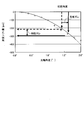
- FIG. 11 is a graph showing the relationship between the optical axis angle and the wavelength shift amount when the optical axis angle is 0 ° when the optical axis is perpendicular to the etalon input surface.
- the wavelength shift amount increases beyond the proportional relationship. For example, when the initial angle of the etalon is 1.4 °, the wavelength shift amount is ⁇ 200 pm. Lock control cannot be performed.
- An object of the present invention is to provide a semiconductor laser module and a suppressing member that can suppress the deviation of the optical axis.
- a semiconductor laser module has a plurality of optical elements optically coupled to each other via at least one base on the temperature control element.
- the distortion of the at least one base is suppressed on at least a part of the strain portion of the at least one base in order to suppress the distortion accompanying the temperature change of the at least one base.
- a suppression member having a linear expansion coefficient of a size that compensates for the linear expansion coefficient of the at least one base is disposed.
- the at least one base includes a first base on which a semiconductor laser element is mounted, at least one optical element, and the first base. And a second base loaded on one base, and the suppression member is disposed on the surface of the first base and / or the second base.
- the magnitude relationship between the linear expansion coefficient of the first base and the linear expansion coefficient of the second base, and the second base is opposite.
- the integrated value of the linear expansion coefficient of the first base and the layer thickness of the first base is on the second base. It is characterized by being substantially equal to or smaller than the integrated value of the linear expansion coefficient of the arranged restraining member and the layer thickness of the restraining member.
- the semiconductor laser module according to the present invention is characterized in that, in the above invention, the suppression member is disposed on a surface where the optical element does not exist and has a shape for suppressing the distortion.
- the end portion to which the optical element of the second base is fixed is stacked on the first base with a single-beam structure.
- another semiconductor laser module is a semiconductor laser module in which a plurality of optical elements are arranged via a plurality of bases above the temperature control element, and at least one of the plurality of bases.
- One base has a linear expansion coefficient that suppresses the distortion of the other base in order to suppress the distortion caused by the temperature change of the other base of the at least one base included in the plurality of bases. It is the suppression layer which has.
- a suppression member for suppressing distortion associated with a temperature change of the plurality of bases is further disposed on a surface of the plurality of bases. It is characterized by.
- the semiconductor laser module according to the present invention is characterized in that, in the above-described invention, the temperature control element and the base on the temperature control element are in contact with each other at a central portion.
- the semiconductor laser module according to the present invention is characterized in that, in the above-mentioned invention, an optical element is further disposed above the suppression member.
- a heat dissipation structure is provided above the suppression member.
- the suppressing member according to the present invention is a suppressing member that suppresses warping of the base that causes warping due to a temperature change, and provides a difference in the linear expansion coefficient of the base. It is characterized by suppressing warping of the base by compensating.
- the base when the base is placed on the temperature control element arranged at the bottom, the warp caused by the difference in linear expansion coefficient between the temperature control element and the base, the base due to this temperature distribution
- a base in which a plurality of plate-like members having two or more layers having different linear expansion coefficients are stacked on the temperature control element, warpage of the plywood of the base due to the difference in the linear expansion coefficient occurs.
- warping is likely to occur on the base on the temperature control element.
- this warpage suppressing structure suppresses the warpage of the base on the temperature control element, it is possible to prevent the optical axis from being shifted between the optical components.
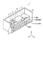
- FIG. 1 is a perspective view showing a configuration of a semiconductor laser module according to Embodiment 1 of the present invention.
- FIG. 2 is an oblique view of the longitudinal section of the semiconductor laser module shown in FIG.
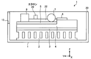
- FIG. 3 is a longitudinal sectional view of the semiconductor laser module shown in FIG.
- FIG. 4 is a longitudinal sectional view showing a configuration of a modification of the semiconductor laser module shown in FIG.
- FIG. 5 is an oblique view of a longitudinal section of a semiconductor laser module according to Embodiment 2 of the present invention.
- 6 is a longitudinal sectional view of the semiconductor laser module shown in FIG.
- FIG. 7 is a longitudinal sectional view showing a configuration of a modification of the semiconductor laser module shown in FIG. FIG.
- FIG. 8 is a longitudinal sectional view showing a configuration of Comparative Example 1 corresponding to Embodiment 1 of the present invention.
- FIG. 9 is a longitudinal sectional view showing a configuration of Comparative Example 2 corresponding to Embodiment 2 of the present invention.
- FIG. 10 is a diagram illustrating the Y-direction position dependency of the Z-direction displacement amount according to the conventional example, the comparative example 1, and the comparative example 2.
- FIG. 11 is a diagram illustrating the relationship between the wavelength shift amount and the optical axis angle.
- a rigid member is used to suppress warping.
- simply stiffening merely increases the warpage depending on the size of the linear expansion coefficient.
- the inventors of the present invention studied the coefficient of linear expansion of a member causing warpage, and suppressed members having a linear expansion coefficient that can compensate for the difference in the coefficient of linear expansion of the member. It was discovered that warpage can be effectively suppressed by using it as a member.
- the present invention is based on this discovery. DESCRIPTION OF EMBODIMENTS
- preferred embodiments of a semiconductor laser module and a suppressing member according to the present invention will be described in detail with reference to the drawings. The present invention is not limited to the embodiments.
- FIG. 1 is a perspective view showing a configuration of a semiconductor laser module according to Embodiment 1 of the present invention.
- FIG. 2 is an oblique view of the longitudinal section of the semiconductor laser module shown in FIG.
- FIG. 3 is a longitudinal sectional view of the semiconductor laser module shown in FIG. 1 to 3, in this semiconductor laser module 1, a Peltier element 2 as a temperature control element is fixedly disposed at the bottom of a housing 20.
- a bonding member 3 made of alumina is bonded to the entire upper surface of the Peltier element 2.
- a plate-like base 4 made of copper tungsten is joined to the entire upper surface of the joining member 3, and a step is formed at one end in the longitudinal direction of the base 4.
- a laser element 6 is arranged.
- An etalon 9 that performs wavelength filtering, a support portion 10 that supports the etalon 9, and a photodetector 11 that detects light that has been wavelength-filtered by the etalon 9 are mounted.
- the base 4, the base 5, and the suppressing member 22 are plate-like members each having a different linear expansion coefficient.
- copper tungsten of the base 4 is 6.65 ⁇ 10 ⁇ 06 (/ ° C. )
- FeNiCo alloy of the base 5 is 4.85 ⁇ 10 -06 (/ °C)
- adjacent plate-like member are different linear expansion coefficient
- the material of each layer is preferably strong against shearing, and as a restraining member, it is necessary that the linear expansion coefficient has a linear expansion coefficient that compensates for the linear expansion coefficient of other layers. More preferably.
- the magnitude of the linear expansion coefficient may be, for example, a plate-like member having an expansion coefficient of large ⁇ small ⁇ large in the order of the base 4 ⁇ the base 5 ⁇ the suppressing member 22, You may laminate
- FIG. even if the plywood structure is composed of a plurality of layers, the plywood structure only needs to have a relationship that compensates for each thermal expansion coefficient.
- Each plate-like member cancels the warp and suppresses the warp, and even if the Peltier element 2 including the joining member 3 is warped, the base 5 and / or the restraining member 22 are less likely to warp, and the beam splitter.
- the optical axis shift between 8 and the etalon 9 hardly occurs. Further, as described above, not only the suppression of warpage due to the thermal expansion of the base 4 and the base 5 but also the suppression member 22 so as to compensate for the warpage caused by the Peltier element 2, the joining member 3, the base 4 and the base 5. May be selected. Thereby, wavelength lock control can be performed with high accuracy.
- the suppressing member 22 can be disposed at a place where an optical element such as the beam splitter 8 on the base 5 is not disposed.
- a shape corresponding to the temperature distribution on the base may be taken so as to give a large suppressing effect to the suppressing member 22.
- the thicknesses of the base 4, the base 5, and the suppressing member 22 are determined by the joining state between the plate-like members and the expansion coefficient. That is, the thicknesses of the adjacent plate-like members are set so that the multiplication value of the volume of the surface where the plate-like members are in contact with the linear expansion coefficient substantially matches.
- the integrated value of the plywood structure and the linear expansion coefficient of the portion where the suppressing member 22 is arranged are close to the integrated value of the thickness of the suppressing member 22 and the linear expansion coefficient, or the integrated value related to the suppressing member is You may set so that it may be a little small. Therefore, for example, as shown in FIG. 3, when the expansion coefficient of the suppression member 22 is smaller than the linear expansion coefficient of the base 4, the thickness of the suppression member 22 is thicker than the thickness of the base 4. It is preferable to use the suppressed member 22a.
- the base 4, the base 5, and the suppressing member 22 may be formed by further forming each plate-like member by a plurality of layers of plate-like members.
- the expansion coefficient may be substantially the same.
- three or more layers of plate-like members having different linear expansion coefficients including the suppressing member 22 may be laminated so as to compensate for warpage.
- a layer for compensating warpage may be newly inserted into the plate-like structure.
- the restraining member 22 of the present invention can be provided on the surface to suppress warpage.
- the optical element such as the etalon 29 may be mounted not only on the base 5 but also on the suppressing member 22. Furthermore, all the optical elements may be mounted on the suppressing member 22. Further, a heat dissipation structure may be provided on the suppression member 22.
- FIG. 5 is an oblique view of a longitudinal section of a semiconductor laser module according to Embodiment 2 of the present invention.
- FIG. 6 is a longitudinal sectional view of the semiconductor laser module shown in FIG. 5 and 6, in the semiconductor laser module 21, a base 24 corresponding to the base 4 is joined to the joining member 3 only at a substantially central portion of the Peltier element 2, and the semiconductor laser element 6 is mounted. The end side and the end side on which the beam splitter 8 and the etalon 9 are mounted are not joined to the joining member 3.
- the region where the semiconductor laser element 6 is mounted on the base 24 is in a cantilever structure and is in a floating state, and the beam splitter 8 and the etalon 9 on the base 25 corresponding to the base 5 are mounted.
- the end region thus formed becomes a cantilever structure and is in a floating state.
- a recess is formed on the base 24, and a convex portion is formed on the base 25, and these recesses and protrusions are fitted.
- the base 24 is slid in the Y direction and coupled to the base 25.
- this fitting structure may also be formed between the joining member 3 and the base 24.
- This fitting can also be designed like a dovetail guide structure.
- the connecting portion between the Peltier element 2 and the base 24 is only at the central portion, the warp of the joint surface of the Peltier element 2 itself affects only the central portion, even if the Peltier element 2 is warped. Even if it occurs, the influence of the warp of the Peltier element 2 on the plywood structure including the bases 24 and 25 is minimized. In this case, the linear expansion coefficient between the bases of the plywood structure may be simply taken into consideration.
- the end portion on which the beam splitter 8 and the etalon 9 or the semiconductor laser 6 are mounted has a cantilever structure, and no warpage occurs on the end side, so that the optical axis shift is less likely to occur. Will be.
- an optical element such as the etalon 29 may be mounted on the suppression member 22 as in the first embodiment.
- FIG. 8 shows the structure of Comparative Example 1 corresponding to the first embodiment.
- the etalon 29 is provided on the base 5 at a position shifted from the optical axis between the condenser lens 7 and the beam splitter 8.
- FIG. 9 shows a comparative example 2 having a cantilever structure corresponding to the second embodiment, and the etalon 29 is placed on the base 25 between the condenser lens 7 and the beam splitter 8. It is provided at a position shifted from the axis.
- a suppression member 22 is provided on the bases 5 and 25.
- both Comparative Examples 1 and 2 form a plywood structure using a plate member having a three-layer structure.
- the semiconductor laser element 6, the beam splitter 8, and the etalon 29 are provided on a base as a plate member having a single layer structure.
- FIG. 10 is a diagram showing the amount of displacement in the Z direction relative to the base-Y direction for Comparative Examples 1 and 2 corresponding to Embodiments 1 and 2 and the conventional example.
- Curves L0, L1, and L2 show the ⁇ Y direction position dependency of the Z direction displacement amount according to the conventional example, the comparative example 1, and the comparative example 2, respectively.
- a large Z-direction displacement of about 15 ⁇ m is generated at the center.
- Comparative Example 1 a Z-direction displacement of about 5 ⁇ m is generated at the center.
- the Z direction displacement of about 10 ⁇ m is relatively generated. Therefore, in the first and second comparative examples, the amount of displacement in the Z direction can be reduced as compared with the conventional example.
- the Y direction angle of the etalon 29 located in the center is substantially 0, whereas in Comparative Example 2, the Y direction angle of the etalon 29 located in the center is Y of the beam splitter 8. It is almost the same value as the direction angle and is tilted in the same direction. That is, in Comparative Example 2, since the displacement of the beam splitter 8 and the etalon 29 has the same inclination, the relative displacement amount (relative displacement angle) between the beam splitter 8 and the etalon 29 is extremely small. I understand that.
- the Y-direction displacement angle of the beam splitter 8 is 0.19 °
- the etalon 29 has a Y-direction displacement angle of 0.01 °.
- the relative displacement angle in the Y direction between the beam splitter 8 and the etalon 29 is 0.18 °.
- the Y-direction displacement angle of the beam splitter 8 is 0.09 °
- the etalon 29 has a Y-direction displacement angle of 0.00 °.
- the beam splitter 8 and the etalon 29 The relative displacement angle in the Y direction is 0.09 °.
- the Y-direction displacement angle of the beam splitter 8 is 0.07 °
- the etalon 29 has a Y-direction displacement angle of 0.03 °.
- the beam splitter 8 and the etalon 29 The relative displacement angle in the Y direction is 0.04 °.
- the Y-direction displacement angle refers to an inclination angle with respect to the Y-axis that is generated by displacement of the optical element in the Z direction.
- the semiconductor laser module and the suppressing member according to the present invention are suitable for applications such as a light source for optical communication.
Landscapes
- Physics & Mathematics (AREA)
- Condensed Matter Physics & Semiconductors (AREA)
- General Physics & Mathematics (AREA)
- Electromagnetism (AREA)
- Optics & Photonics (AREA)
- Optical Couplings Of Light Guides (AREA)
- Semiconductor Lasers (AREA)
Abstract
Description
図1は、この発明の実施の形態1である半導体レーザモジュールの構成を示す斜視図である。また、図2は、図1に示した半導体レーザモジュールの縦断面を斜めからみた図である。さらに、図3は、図1に示した半導体レーザモジュールの縦断面図である。図1~図3において、この半導体レーザモジュール1は、筐体20の底部に温度制御素子としてのペルチェ素子2が固定配置される。このペルチェ素子2の上部全面には、アルミナからなる接合部材3が接合される。さらに、接合部材3の上部全面には銅タングステンからなる板状の基台4が接合され、この基台4の長手方向の一方の端部には段部が形成され、この段部には半導体レーザ素子6が配置される。
図5は、この発明の実施の形態2である半導体レーザモジュールの縦断面を斜めからみた図である。また、図6は、図5に示した半導体レーザモジュールの縦断面図である。図5および図6において、この半導体レーザモジュール21は、基台4に対応する基台24が、ペルチェ素子2の略中央部分のみにおいて接合部材3に接合するとともに、半導体レーザ素子6が搭載される端部側およびビームスプリッタ8およびエタロン9が搭載される端部側が接合部材3に接合しないようにしている。これによって、基台24上の半導体レーザ素子6が搭載される領域は、片持ち梁構造となって浮いた状態となり、基台5に対応する基台25上のビームスプリッタ8およびエタロン9が搭載される端部領域も片持ち梁構造となって浮いた状態となる。
ここで、上述した実施の形態1,2および従来との比較について説明する。図8は、実施の形態1に対応した比較例1の構造を示し、エタロン29を基台5上であって集光レンズ7とビームスプリッタ8との間で光軸からずれた位置に設けている。また、図9は、実施の形態2に対応して片持ち梁構造をもたせた比較例2を示し、エタロン29を基台25上であって集光レンズ7とビームスプリッタ8との間で光軸からずれた位置に設けている。なお、比較例1,2の双方とも、基台5、25上には、抑制部材22を設けている。すなわち、比較例1,2ともに3層構造の板状部材による合板構造を形成している。なお、従来例としては、単層構造の板状部材としての基台上に、半導体レーザ素子6、ビームスプリッタ8、およびエタロン29を設ける。
2 ペルチェ素子
3 接合部材
4,5,24,25 基台
6 半導体レーザ素子
7 集光レンズ
8 ビームスプリッタ
9,29 エタロン
10 支持部
11 光検出器
12 開口部
19 接合部
20 筐体
22,22a 抑制部材
Claims (12)
- 温度制御素子の上部に少なくとも一つの基台を介して、光結合された複数の光学素子が配置された半導体レーザモジュールにおいて、
前記少なくとも一つの基台の温度変化に伴う歪みを抑制するために、前記少なくとも一つの基台の歪み部分の少なくとも一部上に、前記少なくとも一つの基台の歪みを抑制するために、前記少なくとも一つの基台の線膨張係数を補償する大きさの線膨張係数を有する抑制部材を配置したことを特徴とする半導体レーザモジュール。 - 前記少なくとも一つの基台は、半導体レーザ素子を搭載する第1の基台と、少なくとも一つの前記光学素子を搭載し、かつ前記第1の基台上に積載された第2の基台とを含み、前記第1の基台および/または前記第2の基台の表面に前記抑制部材が配置されていることを特徴とする請求項1に記載の半導体レーザモジュール。
- 前記第1の基台の線膨脹係数と前記第2の基台の線膨脹係数との大小関係と、前記第2の基台の線膨脹係数と前記抑制部材の線膨脹係数との大小関係とが逆の関係にあることを特徴とする請求項2に記載の半導体レーザモジュール。
- 前記第1の基台の線膨脹係数と前記第1の基台の層厚との積算値は、前記第2の基台上に配置された前記抑制部材の前記線膨脹係数と該抑制部材の層厚との積算値とほぼ等しいか、あるいは、より小さいことを特徴とする請求項2に記載の半導体レーザモジュール。
- 前記抑制部材は前記光学素子の存在しない表面に配置され、前記歪みを抑制する形状をとることを特徴とする請求項1ないし4のいずれか1項に記載の半導体レーザモジュール。
- 前記第2の基台の光学素子を固定した端部は片もち梁構造で前記第1の基台上に積載されていることを特徴とする請求項2ないし請求項4のいずれか1項に記載の半導体レーザモジュール。
- 温度制御素子の上部に複数の基台を介して、複数の光学素子が配置された半導体レーザモジュールにおいて、
前記複数の基台の中の少なくとも一つの基台は、前記複数の基台に含まれる該少なくとも一つの基台の他の基台の温度変化に伴う線膨張係数の差異から生じる歪みを抑制するために、該他の基台の歪みを抑制する線膨脹係数を有する抑制層であることを特徴とする半導体レーザモジュール。 - 前記複数の基台の表面に、前記複数の基台の温度変化に伴う歪みを抑制するための抑制部材が配置されていることを特徴とする請求項7に記載の半導体レーザモジュール。
- 前記温度制御素子とその上の基台とは中央部周辺のみにおいて接触していることを特徴とする請求項1ないし請求項8のいずれか1項に記載の半導体レーザモジュール。
- 前記抑制部材の上部にはさらに光学素子が配置されていることを特徴とする請求項1ないし請求項9のいずれか1項に記載の半導体レーザモジュール。
- 前記抑制部材の上部には放熱構造が設けられていることを特徴とする請求項1ないし請求項10のいずれか1項に記載の半導体レーザモジュール。
- 温度変化によって反りを生じる基台のそりを抑制する抑制部材であって、基台の線膨脹係数の差異を補償することによって基台のそりを抑制することを特徴とする抑制部材。
Priority Applications (2)
| Application Number | Priority Date | Filing Date | Title |
|---|---|---|---|
| CN2009801581894A CN102362401A (zh) | 2009-03-26 | 2009-09-30 | 半导体激光模块及抑制构件 |
| US13/260,527 US20120020379A1 (en) | 2008-03-31 | 2009-09-30 | Semiconductor laser module and suppression member |
Applications Claiming Priority (2)
| Application Number | Priority Date | Filing Date | Title |
|---|---|---|---|
| JP2009077446A JP2009267386A (ja) | 2008-03-31 | 2009-03-26 | 半導体レーザモジュールおよび抑制部材 |
| JP2009-077446 | 2009-03-26 |
Publications (1)
| Publication Number | Publication Date |
|---|---|
| WO2010109701A1 true WO2010109701A1 (ja) | 2010-09-30 |
Family
ID=42780790
Family Applications (1)
| Application Number | Title | Priority Date | Filing Date |
|---|---|---|---|
| PCT/JP2009/067050 Ceased WO2010109701A1 (ja) | 2008-03-31 | 2009-09-30 | 半導体レーザモジュールおよび抑制部材 |
Country Status (2)
| Country | Link |
|---|---|
| CN (1) | CN102362401A (ja) |
| WO (1) | WO2010109701A1 (ja) |
Families Citing this family (2)
| Publication number | Priority date | Publication date | Assignee | Title |
|---|---|---|---|---|
| WO2017010570A1 (ja) * | 2015-07-16 | 2017-01-19 | 古河電気工業株式会社 | 半導体レーザモジュール |
| JP7421840B2 (ja) * | 2019-02-08 | 2024-01-25 | 古河電気工業株式会社 | 光モジュール |
Citations (5)
| Publication number | Priority date | Publication date | Assignee | Title |
|---|---|---|---|---|
| JP2002148489A (ja) * | 2000-11-07 | 2002-05-22 | Furukawa Electric Co Ltd:The | 半導体レーザモジュールおよびその半導体レーザモジュールを用いたラマンアンプ |
| JP2002333554A (ja) * | 2000-05-31 | 2002-11-22 | Furukawa Electric Co Ltd:The | 半導体レーザモジュール |
| JP2004063915A (ja) * | 2002-07-30 | 2004-02-26 | Kyocera Corp | 光半導体素子収納用パッケージ |
| JP2005167041A (ja) * | 2003-12-04 | 2005-06-23 | Furukawa Electric Co Ltd:The | 温度調節器を有する光学装置およびレーザモジュール |
| JP2007208065A (ja) * | 2006-02-02 | 2007-08-16 | Mitsubishi Electric Corp | 光モジュール |
-
2009
- 2009-09-30 CN CN2009801581894A patent/CN102362401A/zh active Pending
- 2009-09-30 WO PCT/JP2009/067050 patent/WO2010109701A1/ja not_active Ceased
Patent Citations (5)
| Publication number | Priority date | Publication date | Assignee | Title |
|---|---|---|---|---|
| JP2002333554A (ja) * | 2000-05-31 | 2002-11-22 | Furukawa Electric Co Ltd:The | 半導体レーザモジュール |
| JP2002148489A (ja) * | 2000-11-07 | 2002-05-22 | Furukawa Electric Co Ltd:The | 半導体レーザモジュールおよびその半導体レーザモジュールを用いたラマンアンプ |
| JP2004063915A (ja) * | 2002-07-30 | 2004-02-26 | Kyocera Corp | 光半導体素子収納用パッケージ |
| JP2005167041A (ja) * | 2003-12-04 | 2005-06-23 | Furukawa Electric Co Ltd:The | 温度調節器を有する光学装置およびレーザモジュール |
| JP2007208065A (ja) * | 2006-02-02 | 2007-08-16 | Mitsubishi Electric Corp | 光モジュール |
Also Published As
| Publication number | Publication date |
|---|---|
| CN102362401A (zh) | 2012-02-22 |
Similar Documents
| Publication | Publication Date | Title |
|---|---|---|
| US20100303110A1 (en) | Edge Bonded Optical Packages | |
| JP6509451B1 (ja) | 光モジュール | |
| US7783142B2 (en) | Low stress package | |
| JP2009267386A (ja) | 半導体レーザモジュールおよび抑制部材 | |
| CN107850732A (zh) | 具有形成在半导体基板上的多模耦合器的光学模块 | |
| WO2010109701A1 (ja) | 半導体レーザモジュールおよび抑制部材 | |
| CN107851960A (zh) | 半导体激光模块 | |
| JP6265895B2 (ja) | 光素子モジュール | |
| JP2019140306A (ja) | 光モジュール | |
| JP2002232050A (ja) | 光モジュール | |
| US10811840B2 (en) | Laser module | |
| JPWO2020162446A1 (ja) | 光モジュール | |
| CN113805287B (zh) | 光模块 | |
| JP5247795B2 (ja) | 光モジュール | |
| JP2013101244A (ja) | 光モジュール | |
| CN110133807A (zh) | 光模块及光模块的制造方法 | |
| JP5385674B2 (ja) | レーザモジュール | |
| US9323002B2 (en) | Light multiplexer | |
| JP2013205494A (ja) | 光素子モジュール | |
| JP5931687B2 (ja) | マルチチップ光集積モジュール | |
| JP2023536007A (ja) | バックポンピング半導体膜レーザ | |
| KR101143739B1 (ko) | 레이저 광원 장치 | |
| KR102345387B1 (ko) | 다층 구조의 고출력 레이저 다이오드 모듈 | |
| JP2018206899A (ja) | 光増幅器及び光増幅回路装置 | |
| JP2002267875A (ja) | 光モジュール及びその製造方法 |
Legal Events
| Date | Code | Title | Description |
|---|---|---|---|
| WWE | Wipo information: entry into national phase |
Ref document number: 200980158189.4 Country of ref document: CN |
|
| 121 | Ep: the epo has been informed by wipo that ep was designated in this application |
Ref document number: 09842311 Country of ref document: EP Kind code of ref document: A1 |
|
| NENP | Non-entry into the national phase |
Ref country code: DE |
|
| WWE | Wipo information: entry into national phase |
Ref document number: 13260527 Country of ref document: US |
|
| 122 | Ep: pct application non-entry in european phase |
Ref document number: 09842311 Country of ref document: EP Kind code of ref document: A1 |