WO2010107073A1 - 磁気インピーダンス素子およびそれを用いた磁気センサ - Google Patents
磁気インピーダンス素子およびそれを用いた磁気センサ Download PDFInfo
- Publication number
- WO2010107073A1 WO2010107073A1 PCT/JP2010/054588 JP2010054588W WO2010107073A1 WO 2010107073 A1 WO2010107073 A1 WO 2010107073A1 JP 2010054588 W JP2010054588 W JP 2010054588W WO 2010107073 A1 WO2010107073 A1 WO 2010107073A1
- Authority
- WO
- WIPO (PCT)
- Prior art keywords
- magnetic field
- magnetic
- impedance
- impedance element
- sample
- Prior art date
- Legal status (The legal status is an assumption and is not a legal conclusion. Google has not performed a legal analysis and makes no representation as to the accuracy of the status listed.)
- Ceased
Links
Images


Classifications
-
- G—PHYSICS
- G01—MEASURING; TESTING
- G01R—MEASURING ELECTRIC VARIABLES; MEASURING MAGNETIC VARIABLES
- G01R33/00—Arrangements or instruments for measuring magnetic variables
- G01R33/02—Measuring direction or magnitude of magnetic fields or magnetic flux
- G01R33/06—Measuring direction or magnitude of magnetic fields or magnetic flux using galvano-magnetic devices
- G01R33/063—Magneto-impedance sensors; Nanocristallin sensors
Definitions
- the present invention relates to a magnetic impedance element and a magnetic sensor using the same, and more specifically to a magnetic impedance element containing strontium, barium, iron and molybdenum and a magnetic sensor using the same.
- Patent Document 1 Japanese Patent Application Laid-Open No. 11-284249
- Patent Document 2 Japanese Patent Application Laid-Open No. 11-109006
- Patent Document 3 Japanese Patent Application Laid-Open No. 2000-174359
- JP 11-284249 A Japanese Patent Laid-Open No. 11-109006 JP 2000-174359 A
- Patent Document 1 in claim 1, the perovskite type crystal structure represented by the general formula A 2 BB′O 6 is taken, and the A atom occupying the A site in the perovskite type crystal structure is Sr, and the B atom also occupying the B site.
- B ′ atoms are Fe and Mo, and the Fe and Mo atoms have a double aligned perovskite crystal structure in which B sites in the perovskite crystal structure are alternately occupied, and exhibit negative magnetoresistance characteristics
- a magnetoresistive element made of a double aligned perovskite material which is an oxide crystal is disclosed.
- Patent Document 1 a large magnetoresistance change rate can be obtained at low temperatures, but the change rate is small near room temperature or higher, and a large magnetic field is required despite the high ferromagnetic transition temperature. There was a problem.
- Patent Document 2 aims to provide a high-sensitivity magnetic sensor that is small in size, low in cost, excellent in output linearity with respect to a detected magnetic field, and excellent in temperature characteristics, and biased through an insulator layer around a thin film magnetic core. It has a structure in which a coil and a negative feedback coil are wound, and this structure enables the miniaturization and mass production of the magnetic sensor. If the two coils are formed of thin film coils, the efficiency increases, so that a necessary bias magnetic field can be obtained with a small current, and the linearity of the output with respect to the magnetic field can be improved with a small negative feedback amount.
- the thin-film magnetic core is formed of a NiFe or CoFeNi plating film, or an amorphous sputtered film or NiFe sputtered film of CoZrNb, FeSiB, or CoSiB.
- Patent Document 2 the response of the low magnetic field is very good, but the sensing range of the magnetic field is narrow, and the impedance changes positively in the low magnetic field and negative impedance change in the high magnetic field.
- the usable range is limited.
- Patent Document 3 discloses a TMR (tunneling magnetoresistance) element using Sr, Ba, Fe, and Mo oxides.
- Patent Document 3 has a problem that the sensing range is narrow because it works only at a low magnetic field at a low temperature.
- CMR Colossal magnetoresistance
- TMR tunnel magnetoresistance
- AMR anisotropic magnetoagnetoresistance
- GMR giant magnetoresistance
- MI magnetictoimpedance
- the present invention has been made to solve the above-described problems, and an object thereof is to provide a magnetic impedance element having a wide operating range and a magnetic sensor using the same.
- the magneto-impedance element configured as described above can obtain a large rate of change in magnetic impedance at room temperature or higher.
- the larger one of the ratio of the length L to the thickness T of the ceramic body (L / T) or the ratio of L to the width W (L / W) is 1.5 or more.
- a conductor that short-circuits between the external electrode terminals is further provided.
- the magnetic sensor according to the present invention uses any one of the magnetic impedance elements described above.
- the demagnetizing field component can be reduced, the low magnetic field response characteristics can be improved, and the capacitance component can be reduced by forming a penetrating conductor. It is possible to reduce, to improve the MI change rate and to suppress variation.
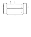
- FIG. 1 is a cross-sectional view of a magneto-impedance element according to Embodiment 1 of the present invention.
- the magneto-impedance element according to the first embodiment of the present invention includes a ceramic body 3 and terminal electrodes 1 and 2 provided on both sides of the ceramic body 3.
- the ratio L / T between the distance between the terminal electrodes 1 and 2 (the length of the ceramic body 3) L and the thickness T of the ceramic body 3, and the width W in the direction perpendicular to the thickness and length is 1.5 or more.
- FIG. 2 is a cross-sectional view of a magneto-impedance element according to Embodiment 2 of the present invention.
- the magneto-impedance element according to the first embodiment is that a through conductor 4 is provided between electrode terminals 1 and 2. And different.
- the through conductor 4 is provided between the electrode terminals 1 and 2
- the capacitance between the electrode terminals 1 and 2 can be reduced.
- the capacity component can be reduced.
- Example 1 The ceramic material was produced by a solid phase reaction method, and the magneto-impedance (MI) element was produced by a general sheet lamination method.
- MI magneto-impedance
- the ceramic material uses barium carbonate (BaCO 3 ), strontium carbonate (SrCO 3 ), iron oxide (Fe 2 O 3 ), and molybdenum oxide (MoO 6 ) as starting materials, and weighed so as to have a desired composition after firing. Then, it was put into a pot together with PSZ balls, ethanol and a dispersant, and pulverized and mixed for 24 hours. After pulverization and mixing, ethanol was evaporated using hot water at a temperature of 80 ° C. to obtain a dry powder. Thereafter, calcination was performed in the atmosphere at a temperature of 800 ° C. for 4 hours to obtain a raw material for sheet forming. At this time, single-phase (Sr, Ba) 2 (Fe, Mo) 2 O 6 is not formed.
- BaCO 3 barium carbonate
- SrCO 3 strontium carbonate
- Fe 2 O 3 iron oxide
- MoO 6 molybdenum oxide
- Sheet raw material powder, a binder, a plasticizer, ethanol, toluene, and a dispersant were prepared in a pot together with PSZ (partially stabilized zirconia) balls and pulverized and mixed to prepare a sheet-forming slurry.
- PSZ partially stabilized zirconia
- a green sheet having a thickness of about 50 ⁇ m was formed from the slurry by a doctor blade method, and then the sheet was cut into a predetermined size.
- a Pd conductor paste was applied on a cut green sheet by a screen printing method, and then dried was inserted.
- the green sheet was laminated and pressure-bonded so as to have a predetermined shape, and cut to a predetermined size to form a green chip.
- the prepared samples were measured for impedance characteristics in the absence of a magnetic field and in a magnetic field using an impedance analyzer (HP4294A) and an electromagnet.
- the magnetic field was applied in parallel with the L direction in which two terminals were formed, and the measurement was performed.
- the composition of the prepared sample is shown in Table 1.
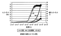
- FIG. 3 and FIG. 4 show the impedance characteristics of sample 1 in Table 1 in the absence of a magnetic field, 1000 G, and 500 G.
- “Initial” in FIG. 3 indicates no magnetic field.
- all of the prepared samples had a low impedance at a low frequency and an impedance increased at a high frequency as shown in FIG.
- the characteristic impedance characteristic of ferromagnetic metal materials is shown.
- the high frequency impedance decreases, and the rate of change reaches about 80% (1000 G) for the element of sample number 1, and a very large rate of change can be obtained with a low magnetic field.
- the impedance hardly changes.
- the magnetic impedance change rate in two magnetic fields of 1000 G and 500 G is calculated by the following equation, and the G rate is determined when the change rate of the magnetic field exceeds 500% at 500 G, and the magnetic field is 1000 G. Even when a large change rate of 20% or more was obtained, it was determined as NG when the magnetic field was 500 G and the change rate was 0%.
- Magnetic impedance (MI) change rate (%) (impedance (no magnetic field) ⁇ impedance (in magnetic field)) / impedance (no magnetic field) ⁇ 100
- Tc ferromagnetic transition temperature
- Table 1 shows the composition and characteristic test results of the prepared samples.
- Sr 2 FeMoO 6 sample sample number 1 having a high Tc
- a large MI change rate of 78% can be obtained in a relatively large magnetic field of 1000 G.
- the rate of change is almost zero in a magnetic field of 500 G (see FIG. 4), and there is a problem with the response of a low magnetic field.
- the MI change rate when the magnetic field is 500 G is drastically improved when Sr: Ba is 1.2: 0.8, and a large change rate of 8% or more can be realized.
- x is 0.8 ⁇ x ⁇ 2.0 MI change rate and the magnetic field of more than 70% magnetic field at 1000G in a range of at 500G An MI change rate of 8% or more can be obtained.
- “*” indicates a comparative example.
- the magnetic impedance characteristic of Sample No. 9 is shown in FIG.
- a magnetic sensor is required not only near room temperature but also at a temperature of + 85 ° C., and a higher ferromagnetic transition temperature (Tc) is desired. Therefore, preferably 0.8 ⁇ x ⁇ 1.7. A range is preferred.
- the Fe / Mo ratio (y / z) does not affect the MI change rate in the magnetic field of 1000 G, but the MI is in the magnetic field of 500 G.
- the high frequency impedance change seen in the element of the present invention is mainly due to the change of the inductor component.
- the inductor (L) component is proportional to its permeability, and the magnetoimpedance effect is manifested by a change in permeability in a magnetic field.
- the resistance (R) component has no frequency dependence, when it is sufficiently small (that is, low resistance like a metal), there is no influence in the high frequency region, but the Fe / Mo ratio is If the layer is excessively large or small, the segregated layer increases the resistance, so the contribution of R is increased, and the change in inductance (L) is apparently reduced to reduce the impedance change rate.
- Example 2 the ceramic composition was the same as that of Sample No. 7 shown in Example 1, and the influence of sample formation on the magnetic impedance characteristics was examined.
- a raw material and a green sheet were prepared in the same manner as in Example 1, and after firing, the sheets were laminated and processed so as to have the length L, width W, and thickness T shown in Table 3, and a terminal electrode was formed after firing to form a sample.
- L was fixed to 2.0 mm
- W was fixed to 1.2 mm
- the sample was evaluated in the same manner as in Example 1 by changing L / T by changing T. The results are shown in Table 3.
- the L / T ratio has a great influence on the magnetic impedance characteristics.
- the rate of change can be realized.
- L / T is smaller than 1.5
- the low magnetic field responsiveness is lowered as compared with a sample having L / T of 1.5 or more. This is due to the influence of the demagnetizing field generated inside the magnetic body when a magnetic field is applied to the magnetic body.
- the magnetic field effectively changes in the magnetic body depending on the sample shape. It is thought that the rate of change of the low magnetic field has decreased.
- the larger of L / T and L / W is 1.5 or more.
- the mechanical strength is extremely lowered or the element resistance is increased.
- Example 3 Next, the effect of a sample in which a conductor for shorting a two-terminal electrode was inserted into a two-terminal single-plate sample was investigated.
- This sample is shown in the structure of FIG.
- a ceramic having the same composition as Sample No. 7 in Example 1 was selected, and a sample was produced in the same manner as in Example 1.
- a through conductor 4 for shorting the two external electrode terminals in the sheet pressing process was inserted, and a sample having a length L of 2 mm, a width W of 1.0 mm, and a thickness T of 0.8 mm was produced.
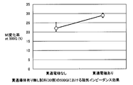
- Thirty samples with and without through-conductors produced were evaluated in the same manner as in Example 1, and the rate of change in magnetic impedance in a 500 G magnetic field was calculated. The result is shown in FIG.
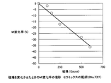
- FIG. 7 is a graph showing the transition of the change rate of MI (magnetoimpedance effect) in the sample number 7 with the magnetic field changed.
- the MI change rate when the frequency is 10 MHz and the magnetic field is changed is shown on the vertical axis.
- the measurement results in FIGS. 4 to 7 show results at room temperature.
Landscapes
- Physics & Mathematics (AREA)
- Chemical & Material Sciences (AREA)
- Engineering & Computer Science (AREA)
- Nanotechnology (AREA)
- Condensed Matter Physics & Semiconductors (AREA)
- General Physics & Mathematics (AREA)
- Hall/Mr Elements (AREA)
- Magnetic Ceramics (AREA)
Abstract
室温以上で大きな磁気インピーダンス効果を得ることが可能な磁気インピーダンス素子を提供するために、磁気インピーダンス素子は、化学式がSr2-xBaxFeyMozO6(0.8≦x≦2.0,y+z=2)で示されるセラミックス素体(3)と、セラミックス素体(3)の両側に設けられた少なくとも2つの電極端子(1,2)とを備える。
Description
この発明は、磁気インピーダンス素子およびそれを用いた磁気センサに関し、より特定的には、ストロンチウム、バリウム、鉄およびモリブデンを含む磁気インピーダンス素子およびそれを用いた磁気センサに関するものである。
従来、磁場を検知できる素子は、たとえば特開平11-284249号公報(特許文献1)、特開平11-109006号公報(特許文献2)および特開2000-174359号公報(特許文献3)に開示されている。
特許文献1では、請求項1において、一般式A2BB′O6で表わされるペロブスカイト型結晶構造をとり、ペロブスカイト型結晶構造中のAサイトを占めるA原子がSr、同じくBサイトを占めるB原子およびB′原子がFeおよびMoであり、なおかつ、FeおよびMo原子がペロブスカイト型結晶構造中のBサイトを交互に占有した二重整列ペロブスカイト型結晶構造であって、負の磁気抵抗特性を示す酸化物結晶体である二重整列ペロブスカイト構造の材料からなる磁気抵抗素子が開示されている。また、請求項2では、Bサイト内におけるMo原子およびFe原子の整列の度合が20%以上であることを特徴とする二重整列ペロブスカイト構造の材料からなる磁気抵抗素子が開示されている。
特許文献1では、低温にて巨大な磁気抵抗変化率が得られるが、強磁性転移温度が高いにもかかわらず、室温付近やそれ以上の温度では変化率が小さく、大きな磁場が必要であるという問題があった。
特許文献2では、小型で低コスト、かつ、検出磁場に対する出力の直線性、温度特性に優れた高感度磁気センサを提供することを目的とし、薄膜磁気コアの周囲に絶縁物層を介してバイアスコイルおよび負帰還コイルを巻回した構造を有し、この構造により磁気センサの小型化および量産化を可能としている。上記の2つのコイルを薄膜コイルで構成すると効率が上がるため、少ない電流で必要なバイアス磁場が得られまた少ない負帰還量で磁場に対する出力の直線性の改善が可能になる。
上記薄膜磁気コアは、NiFe、CoFeNiのめっき膜、あるいはCoZrNb、FeSiB、CoSiBのアモルファススパッタ膜、NiFeスパッタ膜により形成されている。
しかしながら、特許文献2では、低磁場の応答性は非常に優れているが、磁場のセンシング範囲が狭く、また、低磁場ではインピーダンスが正の変化を示し、高磁場で負のインピーダンス変化を示すことから使用できる範囲が限られている。
特許文献3では、Sr、Ba、Fe、Mo酸化物を用いたTMR(tunneling magnetoresistance)素子が開示されている。
しかしながら、特許文献3では、低温で低磁場でしか働かず、センシング範囲が狭いという問題があった。
CMR(Colossal magnetoresistance)材料を用いることにより、これまでにない巨大な磁気抵抗変化を実現することができるが、動作温度が低温に限られ、大きな変化を得るためには数Tオーダの強い磁場が必要であり、実使用温度、磁場を検知するためのセンサとしては使用することができない。また、一方で、低磁場応答可能な磁気センサとしては、TMR(tunneling magnetoresistance)、AMR(anisotropicmagnetoresistance)、GMR(giant magnetoresistance)そしてMI(magnetoimpedance)デバイスなどが既に実用化されており、これらは酸化物ではなく金属の強磁性体や半導体を使用している。非常に低磁場に応答可能である一方で、その磁場の検出範囲が狭いという問題があり、また強い磁場によりすぐに飽和しヒステリシスが発生してしまうなどの問題があり、低磁場から比較的高磁場にかけて動作する磁気センサデバイスが望まれていた。
そこで、この発明は上述のような問題点を解決するためになされたものであり、動作範囲の広い磁気インピーダンス素子およびそれを用いた磁気センサを提供することを目的とする。
この発明に従った磁気インピーダンス素子は、化学式Sr2-xBaxFeyMozO6(0.8≦x≦2.0,y+z=2)で表わされるセラミックス素体と、セラミックス素体に設けられた少なくとも2つの外部電極端子とを備える。
このように構成された磁気インピーダンス素子では、室温以上で、大きな磁気インピーダンス変化率が得られる。
好ましくは、0.8≦x≦1.7である。
好ましくは、セラミックス素体が化学式Sr2-xBaxFeyMozO6(0.8≦x≦1.7,y+z=2,0.9≦y/z≦1.1)で示される。
好ましくは、セラミックス素体が化学式Sr2-xBaxFeyMozO6(0.8≦x≦1.7,y+z=2,0.9≦y/z≦1.1)で示される。
好ましくは、セラミックス素体の長さLと厚みTとの比率(L/T)またはLと幅Wの比率(L/W)のどちらか大きい方が1.5以上である。
この場合、より優れた低磁場応答性およびばらつきを低減することができる。
好ましくは、外部電極端子間を短絡する導体をさらに備える。
好ましくは、外部電極端子間を短絡する導体をさらに備える。
好ましくは、この発明に従った磁気センサは、上述のいずれかの磁気インピーダンス素子を用いる。
セラミックス材料組成を化学式Sr2-xBaxFeyMozO6(0.8≦x≦2.0,y+z=2)の範囲内とすることにより、500G(0.05T)の磁場で20%以上の大きな磁気インピーダンス(MI)変化率を得ることが可能となる。さらに、組成を最適化することにより、携帯電話などで使用される電子部品の保証温度である85℃より高いTcを有しながら500Gの磁場で20%と大きなMI変化率を実現することが可能となる。
さらに、デバイス構造(L/T、L/W)を最適化することにより、反磁場成分を低減し、低磁場応答特性を改善でき、さらに貫通する導体を形成することにより、静電容量成分を低減し、MI変化率の向上およびばらつき抑制を実現することが可能となる。
以下、この発明の実施の形態について、図面を参照して説明する。なお、以下の実施の形態では同一または相当する部分については同一の説明をし、その説明については繰返さない。
(実施の形態1)
図1は、この発明の実施の形態1に従った磁気インピーダンス素子の断面図である。図1を参照して、この発明の実施の形態1に従った磁気インピーダンス素子は、セラミックス素体3と、セラミックス素体3の両側に設けられた端子電極1,2とを有する。セラミックス素体3は、化学式が式Sr2-xBaxFeyMozO6(0.8≦x≦2.0、好ましくは、0.8≦x≦1.7で、かつ0.9≦y/z≦1.1,y+z=2)で示される。
図1は、この発明の実施の形態1に従った磁気インピーダンス素子の断面図である。図1を参照して、この発明の実施の形態1に従った磁気インピーダンス素子は、セラミックス素体3と、セラミックス素体3の両側に設けられた端子電極1,2とを有する。セラミックス素体3は、化学式が式Sr2-xBaxFeyMozO6(0.8≦x≦2.0、好ましくは、0.8≦x≦1.7で、かつ0.9≦y/z≦1.1,y+z=2)で示される。
また、端子電極1,2間の距離(セラミックス素体3の長さ)Lと、セラミックス素体3の厚みTとの比率L/Tと、厚みおよび長さに直交する方向の幅W(図1では示さず)と長さLとの比率L/Wのどちらか大きい方が1.5以上であることが望ましい。
(実施の形態2)
図2は、この発明の実施の形態2に従った磁気インピーダンス素子の断面図である。図2を参照して、この発明の実施の形態2に従った磁気インピーダンス素子では、電極端子1,2間に貫通導体4が設けられている点で、実施の形態1に従った磁気インピーダンス素子と異なる。図2で示すように、実施の形態2に従った磁気インピーダンス素子では、電極端子1,2間に貫通導体4が設けられているため、電極端子1,2間の容量を低減させることができ、容量成分を低減させることができる。
図2は、この発明の実施の形態2に従った磁気インピーダンス素子の断面図である。図2を参照して、この発明の実施の形態2に従った磁気インピーダンス素子では、電極端子1,2間に貫通導体4が設けられている点で、実施の形態1に従った磁気インピーダンス素子と異なる。図2で示すように、実施の形態2に従った磁気インピーダンス素子では、電極端子1,2間に貫通導体4が設けられているため、電極端子1,2間の容量を低減させることができ、容量成分を低減させることができる。
(実施例1)
セラミックス材料は、固相反応法で作製し、磁気インピーダンス(MI)素子は、一般的なシート積層方法で作製した。
セラミックス材料は、固相反応法で作製し、磁気インピーダンス(MI)素子は、一般的なシート積層方法で作製した。
セラミックス材料は出発原料として、炭酸バリウム(BaCO3)、炭酸ストロンチウム(SrCO3)、酸化鉄(Fe2O3)、酸化モリブデン(MoO6)を使用し、焼成後所望の組成となるように秤量し、PSZボール、エタノール、分散剤とともにポットに投入し、粉砕および混合を24時間行なった。粉砕混合の後、温度80℃の温水を用いてエタノールを蒸発させ、乾燥粉末を得た。その後、大気中で温度800℃で4時間の仮焼を行ない、シート成形用の原料を得た。このときは単相の(Sr,Ba)2(Fe,Mo)2O6は形成されていない。
次に、評価デバイスの作製方法について説明する。シート原料粉、バインダ、可塑剤、エタノール、トルエン、分散剤をPSZ(部分安定化ジルコニア)ボールとともにポットに調合、粉砕混合を行ないシート形成のスラリーを作製した。スラリーをドクターブレード法で厚み約50μmのグリーンシートを成形し、その後、所定のサイズにシートを切断した。内部に貫通導体を挿入する場合は、切断したグリーンシート上にPd導体ペーストをスクリーン印刷法で塗布し、その後乾燥させたものを挿入した。
グリーンシートを所定の形状になるように積層および圧着処理を行ない、所定の大きさになるようにカットし、グリーンチップを形成した。
その後、温度400~450℃の大気中で脱バインダ処理を行ない、温度1100-1250℃、N2-H2O-H2雰囲気中で12時間焼成を行ない、(Sr,Ba)2(Fe,Mo)2O6で形成されるセラミックス素体を得た。その後、L方向にAg系外部電極を塗布および形成し、温度700℃でN2-H2雰囲気で焼付け処理を行ない評価用試料を作製した。図1がこの方法で作製した試料である。この実施例では、貫通する導体の入っていない、2端子の素子であり、その素子寸法はL:2.0mm、W:1.2mm、T:0.8mm(L/T=2.5)であった。
次に、本発明の実施例に従ったサンプルにおける効果を調べるために行なった特性試験方法について説明する。作製した試料は、インピーダンスアナライザ(HP4294A)と電磁石を用いて、磁場なしおよび磁場中のインピーダンス特性を測定した。なお、磁場は2端子が形成されたL方向と平行に印加して測定を行なった。このとき、用意した試料の組成を表1に示す。

なお、表1に記載の試料1~12では、y=z=1.0である。
表1中の試料1の無磁場、1000G、500G中でのインピーダンス特性を代表して図3および図4で示す。
表1中の試料1の無磁場、1000G、500G中でのインピーダンス特性を代表して図3および図4で示す。
図3における「初期」は無磁場を示す。
作製した試料はすべて、無磁場中では図3で示すように、低周波でインピーダンスが小さく、高周波にかけてインピーダンスが増大した。強磁性金属材料に特徴的なインピーダンス特性を示した。磁場を素子の長手方向に印加すると、高周波のインピーダンスが低下し、その変化率は試料番号1の素子で約80%(1000G)に達し、低磁場で非常に大きな変化率を得ることができる。ちなみに長手方向に直交する方向に磁場を印加してもインピーダンスはほとんど変化しない。この実施例では、磁場が1000G、500Gの2つの磁場中での磁気インピーダンス変化率を次式で算出し、磁場が500Gでの変化率が0%を超えるものをG判定とし、磁場が1000Gで20%以上の大きな変化率が得られても磁場が500Gで変化率が0%の場合はNGと判定した。
作製した試料はすべて、無磁場中では図3で示すように、低周波でインピーダンスが小さく、高周波にかけてインピーダンスが増大した。強磁性金属材料に特徴的なインピーダンス特性を示した。磁場を素子の長手方向に印加すると、高周波のインピーダンスが低下し、その変化率は試料番号1の素子で約80%(1000G)に達し、低磁場で非常に大きな変化率を得ることができる。ちなみに長手方向に直交する方向に磁場を印加してもインピーダンスはほとんど変化しない。この実施例では、磁場が1000G、500Gの2つの磁場中での磁気インピーダンス変化率を次式で算出し、磁場が500Gでの変化率が0%を超えるものをG判定とし、磁場が1000Gで20%以上の大きな変化率が得られても磁場が500Gで変化率が0%の場合はNGと判定した。
磁気インピーダンス(MI)変化率(%)=(インピーダンス(無磁場)-インピーダンス(磁場中))/インピーダンス(無磁場)×100
また強磁性転移温度(Tc)を調べるため、VSM(Vibrating Sample Magnetometer)を用いて、磁化率の温度依存性から大まかなTcを見積もった。
また強磁性転移温度(Tc)を調べるため、VSM(Vibrating Sample Magnetometer)を用いて、磁化率の温度依存性から大まかなTcを見積もった。
作製した試料の組成と特性試験結果が表1に示されている。
表1から明らかであるように、高いTcを有する式Sr2FeMoO6試料(試料番号1)では、1000Gと比較的大きな磁場中では78%に達する大きなMI変化率を得ることができているが、磁場が500G中の磁場中では変化率がほぼ0であり(図4参照)、低磁場の応答性に問題がある。SrサイトをBaで置換していくとSr:Baが1.2:0.8のときに急激に磁場が500GでのMI変化率が改善され、8%以上の大きな変化率を実現できる。したがって、セラミックスの組成が化学式Sr2-xBaxFeMoO6で示されるとき、xが0.8≦x≦2.0の範囲で磁場が1000Gで70%以上のMI変化率と磁場が500Gで8%以上のMI変化率を得ることができる。表において「*」は比較例であることを示している。
表1から明らかであるように、高いTcを有する式Sr2FeMoO6試料(試料番号1)では、1000Gと比較的大きな磁場中では78%に達する大きなMI変化率を得ることができているが、磁場が500G中の磁場中では変化率がほぼ0であり(図4参照)、低磁場の応答性に問題がある。SrサイトをBaで置換していくとSr:Baが1.2:0.8のときに急激に磁場が500GでのMI変化率が改善され、8%以上の大きな変化率を実現できる。したがって、セラミックスの組成が化学式Sr2-xBaxFeMoO6で示されるとき、xが0.8≦x≦2.0の範囲で磁場が1000Gで70%以上のMI変化率と磁場が500Gで8%以上のMI変化率を得ることができる。表において「*」は比較例であることを示している。
参考に試料番号9の磁気インピーダンス特性を図5で示す。
また、近年磁気センサも室温付近だけでなく、温度+85℃での保証が必要とされ、強磁性転移温度(Tc)もそれ以上が望まれるため、好ましくは0.8≦x≦1.7の範囲が好ましい。
また、近年磁気センサも室温付近だけでなく、温度+85℃での保証が必要とされ、強磁性転移温度(Tc)もそれ以上が望まれるため、好ましくは0.8≦x≦1.7の範囲が好ましい。
次に、強磁性転移温度(Tc)が85℃よりも高い組成範囲(x≦1.7)でFe/Mo比率(y/z)の影響について調査を行なった。特性試験結果を表2に示す。

表2から明らかなように、1.0≦x≦1.7の範囲内において、Fe/Mo比(y/z)は1000Gの磁場におけるMI変化率には影響しないものの、磁場が500GではMI変化率に大きく影響し、0.9≦y/z≦1.1の範囲では500Gの磁場中でのMI変化率も20%以上となり、組成によってはy/z=1.0組成より変化率が大きくなるものも確認できる。しかし、0.9≦y/z≦1.1の範囲を外れると0.9≦y/z≦1.1の範囲内のサンプルと比較してMI変化率が低下してしまうことがわかる。これらの原因は明らかではないが、粉末X線回折から、Fe/Mo比が0.9≦y/z≦1.1の範囲を外れると、SrFeO3やSrMoO4などの不純物が形成されることが明らかになっており、これらが粒界に偏析して試料自体の抵抗が上がってしまい、低磁場への応答性が低下したものと推測される。
本発明の素子に見られる高周波のインピーダンス変化は、主にインダクタ成分の変化に起因している。
Z=R+jωL+1/jωC
強磁性体の場合、インダクタ(L)成分はその透磁率に比例し、磁気インピーダンス効果は、磁場中での透磁率の変化により発現している。しかし、上式から明らかであるように、抵抗(R)成分に周波数依存性がないために、十分小さい場合(つまり金属のように低抵抗)は高周波領域で影響しないが、Fe/Mo比が過度に大きい、または小さい場合には偏析した層が抵抗を上げてしまうためRの寄与が大きくなり、インダクタンス(L)の変化が見かけ上小さくなってインピーダンス変化率が小さくなるものと考えられる。
強磁性体の場合、インダクタ(L)成分はその透磁率に比例し、磁気インピーダンス効果は、磁場中での透磁率の変化により発現している。しかし、上式から明らかであるように、抵抗(R)成分に周波数依存性がないために、十分小さい場合(つまり金属のように低抵抗)は高周波領域で影響しないが、Fe/Mo比が過度に大きい、または小さい場合には偏析した層が抵抗を上げてしまうためRの寄与が大きくなり、インダクタンス(L)の変化が見かけ上小さくなってインピーダンス変化率が小さくなるものと考えられる。
(実施例2)
次に、セラミックス組成を実施例1で示す試料番号7と同じ組成で、試料形成の磁気インピーダンス特性への影響を調べた。実施例1と同じ方法で原料およびグリーンシートを作製し、焼成後表3に示す長さL、幅Wおよび厚みTになるようにシート積層、加工を行ない、焼成後に端子電極を形成して試料を得た。本実施例では、Lを2.0mm、Wを1.2mmと固定し、Tを変化させることによりL/Tを変化させ試料を実施例1と同様の方法で評価した。その結果を表3に示す。
次に、セラミックス組成を実施例1で示す試料番号7と同じ組成で、試料形成の磁気インピーダンス特性への影響を調べた。実施例1と同じ方法で原料およびグリーンシートを作製し、焼成後表3に示す長さL、幅Wおよび厚みTになるようにシート積層、加工を行ない、焼成後に端子電極を形成して試料を得た。本実施例では、Lを2.0mm、Wを1.2mmと固定し、Tを変化させることによりL/Tを変化させ試料を実施例1と同様の方法で評価した。その結果を表3に示す。
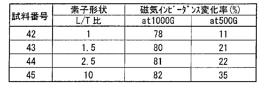
表3から明らかであるように、L/T比が磁気インピーダンス特性に大きく影響し、L/T比が1.5以上であれば本発明の目的とする低磁場から高磁場の幅広い範囲において大きな変化率を実現することができる。しかし、L/Tが1.5より小さくなるとL/Tが1.5以上のサンプルと比較して低磁場応答性が低下する。これは、磁性体に磁場を印加した際に磁性体内部に発生する反磁場の影響で、磁性体に有効に磁場が試料形状により変化し、反磁場が大きくなる、L/Tが小さい試料では低磁場の変化率が低下したと考えられる。本発明の材料組成の特徴を十分活かした作製するためには試料形状にも十分注意をする必要があり、L/TとL/Wのどちらか大きい方が1.5以上とすることが好ましい。一方で、あまり大きくしすぎると、機械的強度が極端に低下したり、素子抵抗が上昇する。組成にもよるが、おおむね20以下であることが望ましい。
(実施例3)
次に、2端子の単板形状試料に2端子電極をショートする導体を挿入した試料の効果について調査を行なった。なお、この試料は図2の構造で示される。試料は実施例2と同様に実施例1の試料番号7と同じ組成のセラミックスを選択し、実施例1と同様の方法で試料を作製した。シート圧着行程で2つの外部電極端子をショートさせる貫通導体4を挿入し、長さLが2mm、幅Wが1.0mm、厚みTが0.8mmの寸法を有する試料を作製した。作製した貫通導体あり、なしの試料をそれぞれ30個、実施例1と同様の方法で評価し、500Gの磁場での磁気インピーダンス変化率を算出した。その結果を図6に示す。
次に、2端子の単板形状試料に2端子電極をショートする導体を挿入した試料の効果について調査を行なった。なお、この試料は図2の構造で示される。試料は実施例2と同様に実施例1の試料番号7と同じ組成のセラミックスを選択し、実施例1と同様の方法で試料を作製した。シート圧着行程で2つの外部電極端子をショートさせる貫通導体4を挿入し、長さLが2mm、幅Wが1.0mm、厚みTが0.8mmの寸法を有する試料を作製した。作製した貫通導体あり、なしの試料をそれぞれ30個、実施例1と同様の方法で評価し、500Gの磁場での磁気インピーダンス変化率を算出した。その結果を図6に示す。
図6から明らかなように、貫通導体を有していない試料でもすべて15%以上の変化率を得ることができるが、ばらつきが大きい問題がある。これは、多結晶体粒界の静電容量成分、抵抗成分が不均一になりがちであり、これらの影響によりばらつきが生じているものと推測される。また、高周波になるに従い、その信号は表層部に集中することが知られており(表皮効果)、比較的粒径分布が不均一になりがちな表面の微細構造の影響や、還元処理焼成による表層部の変質などが影響している可能性が考えられる。一方、貫通導体を形成した試料では、低磁場での磁気インピーダンス変化率が少し改善され、ばらつきも低減される。この効果の原因については明らかではないが、磁場に対して応答するSMFO系セラミックス素体に対して並列に接続された低抵抗体となるため、上述したセラミックスならではの不均一性を貫通導体が低減しているものと推測される。
図7は、試料番号7において、磁場を変化させた状態におけるMI変化率(magnetoimpedance effect)の推移を示すグラフである。周波数を10MHzとして磁場を変化させた場合におけるMI変化率を縦軸に示している。なお、図4から図7の測定結果は、室温での結果を示している。
今回開示された実施の形態および実施例はすべての点で例示であって制限的なものではないと考えられるべきである。本発明の範囲は上記した説明ではなくて請求の範囲によって示され、請求の範囲と均等の意味および範囲内でのすべての変更が含まれることが意図される。
1,2 端子電極、3 セラミックス素体、4 貫通導体。
Claims (6)
- 化学式Sr2-xBaxFeyMozO6(0.8≦x≦2.0,y+z=2)で表わされるセラミックス素体(3)と、
前記セラミックス素体に設けられた少なくとも2つの外部電極端子(1,2)とを備えた、磁気インピーダンス素子。 - 0.8≦x≦1.7である、請求の範囲第1項に記載の磁気インピーダンス素子。
- 前記セラミックス素体が化学式Sr2-xBaxFeyMozO6(0.8≦x≦1.7,y+z=2,0.9≦y/z≦1.1)で示される、請求の範囲第1項に記載の磁気インピーダンス素子。
- 前記セラミックス素体の長さLと厚みTとの比率(L/T)または長さLと幅Wの比率(L/W)のどちらか大きい方が1.5以上である、請求の範囲第1項に記載の磁気インピーダンス素子。
- 前記少なくとも2つの外部電極端子間を短絡する導体(4)をさらに備えた、請求の範囲第1項に記載の磁気インピーダンス素子。
- 請求の範囲第1項に記載の磁気インピーダンス素子を用いた磁気センサ。
Priority Applications (2)
| Application Number | Priority Date | Filing Date | Title |
|---|---|---|---|
| JP2011504872A JP5375951B2 (ja) | 2009-03-19 | 2010-03-17 | 磁気インピーダンス素子およびそれを用いた磁気センサ |
| US13/232,359 US8710835B2 (en) | 2009-03-19 | 2011-09-14 | Magnetic impedance element and magnetic sensor using the same |
Applications Claiming Priority (2)
| Application Number | Priority Date | Filing Date | Title |
|---|---|---|---|
| JP2009-067814 | 2009-03-19 | ||
| JP2009067814 | 2009-03-19 |
Related Child Applications (1)
| Application Number | Title | Priority Date | Filing Date |
|---|---|---|---|
| US13/232,359 Continuation US8710835B2 (en) | 2009-03-19 | 2011-09-14 | Magnetic impedance element and magnetic sensor using the same |
Publications (1)
| Publication Number | Publication Date |
|---|---|
| WO2010107073A1 true WO2010107073A1 (ja) | 2010-09-23 |
Family
ID=42739732
Family Applications (1)
| Application Number | Title | Priority Date | Filing Date |
|---|---|---|---|
| PCT/JP2010/054588 Ceased WO2010107073A1 (ja) | 2009-03-19 | 2010-03-17 | 磁気インピーダンス素子およびそれを用いた磁気センサ |
Country Status (3)
| Country | Link |
|---|---|
| US (1) | US8710835B2 (ja) |
| JP (1) | JP5375951B2 (ja) |
| WO (1) | WO2010107073A1 (ja) |
Families Citing this family (1)
| Publication number | Priority date | Publication date | Assignee | Title |
|---|---|---|---|---|
| JP2021036199A (ja) * | 2017-10-06 | 2021-03-04 | 株式会社村田製作所 | 磁気センサ及び電流センサ |
Citations (3)
| Publication number | Priority date | Publication date | Assignee | Title |
|---|---|---|---|---|
| JPH10233541A (ja) * | 1996-12-18 | 1998-09-02 | Tokin Corp | 磁気検出素子 |
| JP2000174359A (ja) * | 1998-12-09 | 2000-06-23 | Toshiba Corp | 磁気抵抗素子 |
| JP2005062000A (ja) * | 2003-08-12 | 2005-03-10 | Sankyo Seiki Mfg Co Ltd | 磁気検出素子および磁気検出回路 |
Family Cites Families (8)
| Publication number | Priority date | Publication date | Assignee | Title |
|---|---|---|---|---|
| JPH1022129A (ja) | 1996-06-28 | 1998-01-23 | Tokin Corp | 積層型インピーダンス素子 |
| JP4047955B2 (ja) | 1997-10-01 | 2008-02-13 | ミネベア株式会社 | 磁気インピーダンスセンサ |
| JP2981661B2 (ja) | 1998-03-27 | 1999-11-22 | 工業技術院長 | 二重整列ペロブスカイト構造磁気抵抗素子 |
| WO2001077024A1 (en) * | 2000-04-06 | 2001-10-18 | Rutgers, The State University | CHEMICAL-PRESSURE TAILORING OF LOW-FIELD, ROOM TEMPERATURE MAGNETORESISTANCE IN (Ca, Sr, Ba) Fe0.5Mo0.5O¿3? |
| JP3953800B2 (ja) | 2001-12-07 | 2007-08-08 | 修 木村 | 高周波用磁性材料 |
| JP2006286713A (ja) | 2005-03-31 | 2006-10-19 | Osaka Univ | 磁気抵抗素子および磁化反転方法 |
| JP2007027493A (ja) | 2005-07-19 | 2007-02-01 | Nec Corp | 磁気抵抗効果素子およびその製造方法 |
| JP4550713B2 (ja) | 2005-10-21 | 2010-09-22 | 株式会社東芝 | 磁気抵抗効果素子の製造方法 |
-
2010
- 2010-03-17 WO PCT/JP2010/054588 patent/WO2010107073A1/ja not_active Ceased
- 2010-03-17 JP JP2011504872A patent/JP5375951B2/ja not_active Expired - Fee Related
-
2011
- 2011-09-14 US US13/232,359 patent/US8710835B2/en active Active
Patent Citations (3)
| Publication number | Priority date | Publication date | Assignee | Title |
|---|---|---|---|---|
| JPH10233541A (ja) * | 1996-12-18 | 1998-09-02 | Tokin Corp | 磁気検出素子 |
| JP2000174359A (ja) * | 1998-12-09 | 2000-06-23 | Toshiba Corp | 磁気抵抗素子 |
| JP2005062000A (ja) * | 2003-08-12 | 2005-03-10 | Sankyo Seiki Mfg Co Ltd | 磁気検出素子および磁気検出回路 |
Non-Patent Citations (1)
| Title |
|---|
| K.-I. KOBAYASHI ET AL.: "Room-temperature magnetoresistance in an oxide material with an ordered double-perovskite structure", NATURE, vol. 395, 15 October 1998 (1998-10-15), pages 677 - 680 * |
Also Published As
| Publication number | Publication date |
|---|---|
| JPWO2010107073A1 (ja) | 2012-09-20 |
| JP5375951B2 (ja) | 2013-12-25 |
| US8710835B2 (en) | 2014-04-29 |
| US20120001626A1 (en) | 2012-01-05 |
Similar Documents
| Publication | Publication Date | Title |
|---|---|---|
| Mazumdar et al. | Tuning of magnetoelectric coupling in (1− y) Bi0. 8Dy0. 2FeO3–yNi0. 5Zn0. 5Fe2O4 multiferroic composites | |
| Kostishyn et al. | Synthesis and multiferroic properties of M-type SrFe12O19 hexaferrite ceramics | |
| Kobayashi et al. | Possible percolation and magnetoresistance in ordered double perovskite alloys Sr2Fe (W1− xMox) O6 | |
| Zhang et al. | Influences of annealing temperature on structural characterization and magnetic properties of Mn-doped BaTiO3 ceramics | |
| Khanduri et al. | Structural, dielectric, magnetic, and nuclear magnetic resonance studies of multiferroic Y-type hexaferrites | |
| Rodrigues et al. | Study of the structural, dielectric and magnetic properties of Bi2O3 and PbO addition on BiFeO3 ceramic matrix | |
| Mazumdar et al. | Enhanced multiferroic properties in (1–y) BiFeO3–yNi0. 50Cu0. 05Zn0. 45Fe2O4 composites | |
| Das et al. | An experimental insight of the multiferroic properties of magnetoelectrically coupled xLNCZFO+ (1− x) BSTDO composites | |
| Momin et al. | Enhance magnetoelectric coupling in xLi0. 1Ni0. 2Mn0. 6Fe2. 1O4–(1− x) BiFeO3 multiferroic composites | |
| Li et al. | Dielectric, multiferroic and magnetodielectric properties of (1-x) BaTiO3-xSr2CoMoO6 solid solution | |
| JP2783788B2 (ja) | 温度センサー用フェライト素子 | |
| Khasskhoussi et al. | Improved dielectric and ferromagnetic properties of Fe-site substituted rhombohedral structured BiFeO3 ceramic | |
| Chen et al. | Room temperature magnetoelectric effect of YFeO3–Y3Fe5O12 ferrite composites | |
| Bhuiyan et al. | Correlations of structural, dielectric, magnetic and magnetoelectric properties of Ca1-xSrx (Fe0. 5Ta0. 5) O3 multiferroic ceramics | |
| Deac et al. | Electroresistance, magnetocapacitance and magnetotransport properties of La0. 55Ca0. 45MnO3/BaTiO3 composite | |
| JP5375951B2 (ja) | 磁気インピーダンス素子およびそれを用いた磁気センサ | |
| Goel et al. | Investigations on magnetoelectric response in binary ferroelectric {0.94 Na0. 5Bi0. 5TiO3 (NBT)-0.06 Ba0. 85Sr0. 15Zr0. 1Ti0. 9O3 (BSZT)}-ferrimagnetic (NiFe2O4) particulate composites | |
| Hossain et al. | Structural and electro-magnetic properties of low temperature co-fired BaSrTiO3 and NiCuZn ferrite composites for EMI filter applications | |
| US9947460B2 (en) | Oxide ceramic and ceramic electronic component | |
| JP5884917B2 (ja) | 酸化物セラミックス、及びセラミック電子部品 | |
| Thang et al. | Structural, magnetic and electric properties of Nd and Ni co-doped BiFeO3 materials | |
| Dwevedi et al. | Magnetoreactance studies in rare earth-doped Ni ferrite | |
| JP5493278B2 (ja) | 強磁性セラミック、ならびにそれを用いて構成される磁気抵抗素子および磁気センサ | |
| JP6150061B2 (ja) | 酸化物セラミックスの製造方法、酸化物セラミックス、及びセラミック電子部品 | |
| US10497499B2 (en) | Oxide ceramic and ceramic electronic component |
Legal Events
| Date | Code | Title | Description |
|---|---|---|---|
| 121 | Ep: the epo has been informed by wipo that ep was designated in this application |
Ref document number: 10753564 Country of ref document: EP Kind code of ref document: A1 |
|
| WWE | Wipo information: entry into national phase |
Ref document number: 2011504872 Country of ref document: JP |
|
| NENP | Non-entry into the national phase |
Ref country code: DE |
|
| 122 | Ep: pct application non-entry in european phase |
Ref document number: 10753564 Country of ref document: EP Kind code of ref document: A1 |