WO2010107071A1 - 画像表示装置 - Google Patents
画像表示装置 Download PDFInfo
- Publication number
- WO2010107071A1 WO2010107071A1 PCT/JP2010/054584 JP2010054584W WO2010107071A1 WO 2010107071 A1 WO2010107071 A1 WO 2010107071A1 JP 2010054584 W JP2010054584 W JP 2010054584W WO 2010107071 A1 WO2010107071 A1 WO 2010107071A1
- Authority
- WO
- WIPO (PCT)
- Prior art keywords
- scanning element
- waveform
- speed scanning
- drive signal
- resonance frequency
- Prior art date
- Legal status (The legal status is an assumption and is not a legal conclusion. Google has not performed a legal analysis and makes no representation as to the accuracy of the status listed.)
- Ceased
Links
Images






Classifications
-
- H—ELECTRICITY
- H04—ELECTRIC COMMUNICATION TECHNIQUE
- H04N—PICTORIAL COMMUNICATION, e.g. TELEVISION
- H04N3/00—Scanning details of television systems; Combination thereof with generation of supply voltages
- H04N3/02—Scanning details of television systems; Combination thereof with generation of supply voltages by optical-mechanical means only
- H04N3/08—Scanning details of television systems; Combination thereof with generation of supply voltages by optical-mechanical means only having a moving reflector
-
- G—PHYSICS
- G02—OPTICS
- G02B—OPTICAL ELEMENTS, SYSTEMS OR APPARATUS
- G02B26/00—Optical devices or arrangements for the control of light using movable or deformable optical elements
- G02B26/08—Optical devices or arrangements for the control of light using movable or deformable optical elements for controlling the direction of light
- G02B26/10—Scanning systems
- G02B26/105—Scanning systems with one or more pivoting mirrors or galvano-mirrors
-
- G—PHYSICS
- G09—EDUCATION; CRYPTOGRAPHY; DISPLAY; ADVERTISING; SEALS
- G09G—ARRANGEMENTS OR CIRCUITS FOR CONTROL OF INDICATING DEVICES USING STATIC MEANS TO PRESENT VARIABLE INFORMATION
- G09G3/00—Control arrangements or circuits, of interest only in connection with visual indicators other than cathode-ray tubes
- G09G3/02—Control arrangements or circuits, of interest only in connection with visual indicators other than cathode-ray tubes by tracing or scanning a light beam on a screen
-
- H—ELECTRICITY
- H04—ELECTRIC COMMUNICATION TECHNIQUE
- H04N—PICTORIAL COMMUNICATION, e.g. TELEVISION
- H04N9/00—Details of colour television systems
- H04N9/12—Picture reproducers
- H04N9/31—Projection devices for colour picture display, e.g. using electronic spatial light modulators [ESLM]
- H04N9/3129—Projection devices for colour picture display, e.g. using electronic spatial light modulators [ESLM] scanning a light beam on the display screen
Definitions
- the present invention relates to an image display device that displays an image by two-dimensionally scanning light corresponding to an image signal.
- an optical scanning type image display apparatus that displays light by two-dimensionally scanning light generated based on an image signal (hereinafter referred to as “image light”) using an optical scanning element such as a galvanometer mirror.
- image light an image signal
- an optical scanning element such as a galvanometer mirror
- this type of image display apparatus scans image light in a horizontal direction with a reflection mirror of an optical scanning element that performs high-speed scanning (hereinafter referred to as “high-speed scanning element”), and then performs the horizontal scanning.
- the two-dimensionally scanned image is displayed by scanning the image light in the vertical direction with a reflection mirror of an optical scanning element that performs low-speed scanning (hereinafter referred to as “low-speed scanning element”).
- Patent Document 1 discloses that an image scanned in the horizontal direction by scanning the image light in the horizontal direction by causing the reflection mirror of the resonance type high-speed scanning element (main scanning element) to oscillate at the resonance frequency fr.
- a display device is disclosed.
- the resonance frequency fr of the high-speed scanning element often deviates from the design value due to individual characteristics (individual structure variation) and environmental characteristics such as temperature. As described above, although there are variations such as individual differences in the resonance frequency fr of the high-speed scanning element, in order to perform stable image display, the drive frequency of the reflection mirror of the low-speed scanning element is synchronized with the resonance frequency fr of the high-speed scanning element. It is necessary to let
- the scanning cycle of the low-speed scanning element shifts with a change in the resonance frequency fr of the high-speed scanning element.
- the resonance frequency fr of the high-speed scanning element is increased by 10%
- the driving frequency (scanning frequency) of the low-speed scanning element driven synchronously with the high-speed scanning element is also increased by 10%.
- the vertical synchronization frequency (frame frequency) of an image signal supplied from an external device or the like is determined in advance (generally 30 frames / second or 60 frames / second)
- the driving frequency of the low-speed scanning element is the vertical synchronization frequency.
- a period obtained by accumulating the number of effective scanning lines in one scanning period of the high-speed scanning element is set as an effective scanning period for effectively scanning the image light, and is effective from the driving period of the low-speed scanning element.
- a period obtained by subtracting the scanning period is set as an invalid scanning period in which image light is not scanned effectively, and the driving cycle (frame cycle) of the reflection mirror of the low-speed scanning element is made constant.
- Patent Document 1 drives a reflection mirror of a low-speed scanning element with a step motor, and although it is easy to sequentially drive the reflection mirror by a predetermined amount in accordance with a clock signal, scanning is performed. High speed operation with a large number of lines is not suitable due to problems such as step-outs.
- an electromagnetic optical scanning element is often employed. However, an electromagnetic optical scanning element forms a sawtooth drive waveform and drives it as a drive signal. The technique using the step motor described in Document 1 cannot be applied.
- optical scanning may not be performed properly simply by changing the invalid scanning period.
- the low-speed scanning element when a scanning element in which a reflecting mirror is swingably supported by a fixed member via an elastic beam member is used as a low-speed scanning element, the low-speed scanning element has an inherent resonance determined by the characteristics of the reflecting mirror and the beam member. There is a frequency. For this reason, when such a scanning element is used as a low-speed scanning element, if the drive signal for driving the low-speed scanning element includes a resonance frequency unique to the low-speed scanning element, resonance vibration of the reflection mirror is induced. Then, this resonance vibration causes unnecessary frequency component oscillation to be superimposed on the oscillation of the reflecting mirror, and there arises a situation where optical scanning faithful to the drive signal cannot be realized.
- the present invention stabilizes the oscillation period of the low-speed scanning element in the image display device using the high-speed scanning element whose resonance frequency changes and the low-speed scanning element having a specific resonance frequency.
- the object is to suppress the induction of resonance vibration of the reflection mirror.
- an image display device that displays an image by two-dimensionally scanning light having an intensity corresponding to an image signal
- the light having an intensity corresponding to the image signal is displayed.
- a light source unit that emits light, a resonance type high-speed scanning element that scans light incident by a resonance mirror that oscillates at a relatively high speed in the first direction, and a direction according to the signal level of the input drive signal
- a low-speed scanning element that tilts the reflection mirror and scans light incident on the reflection mirror in a second direction substantially orthogonal to the first direction at a relatively low speed
- a detection unit that detects a resonance frequency of the high-speed scanning element
- a drive signal generation unit that generates a drive signal having a sawtooth waveform according to the resonance frequency of the high-speed scanning element, and a low-speed scanning element drive that inputs the drive signal generated by the drive signal generation unit to the low-speed scanning element Part , Comprising a.
- the drive signal generator stores data of a first waveform for effective scanning of light among the sawtooth waveform of the drive signal, and is a waveform excluding the first waveform of the sawtooth waveform of the drive signal.
- Storage means for storing data of the second waveform, and sequentially reading out the data of the first waveform stored in the storage means at a read timing according to the resonance frequency of the high-speed scanning element, and the drive signal of the first waveform portion
- the second waveform data is sequentially read at the read timing according to the resonance frequency of the high-speed scanning element, and the drive signal of the second waveform portion according to the resonance frequency of the high-speed scanning element is generated.
- the fluctuation of the period of the sawtooth waveform is maintained within a predetermined time.
- the second waveform a waveform in which the component of the resonance frequency unique to the low speed scanning element is suppressed, it is possible to suppress the induction of the resonance vibration of the reflection mirror of the low speed scanning element.
- the drive signal generation unit may be configured such that the total number of data of the first waveform portion read at the read timing is constant, while the total number of data of the second waveform portion read at the read timing is It can be changed according to the resonance frequency of the high-speed scanning element.
- Such a configuration makes it easy to maintain the periodic fluctuation of the sawtooth waveform within a predetermined range.
- the storage unit stores a plurality of types of data of the second waveform according to the resonance frequency of the high-speed scanning element
- the drive signal generation unit includes the resonance frequency of the high-speed scanning element.
- the data of the second waveform of the type corresponding to can be read out from the storage means, and the drive signal of the second waveform portion can be generated.
- the load associated with the data selection process can be reduced as compared with the case where the data of the second waveform is one type and a part of the data is selected and extracted.
- the degree of freedom is high compared to selecting and extracting a part of data, and the second waveform portion can be easily formed into a waveform in which the resonance frequency component specific to the low-speed scanning element is suppressed.
- the period of the readout timing may be a time that is 1 ⁇ 2 of the oscillation period of the high-speed scanning element or an integral multiple thereof, and does not suppress the frequency band of the drive signal. it can.
- the predetermined time can be a time of one scanning cycle by the high-speed scanning element.
- the fluctuation of the oscillation period (low speed scanning period) of the low speed scanning element due to the fluctuation of the resonance frequency of the high speed scanning element can be reduced most.
- the light source unit changes the luminance of light according to the image signal according to the resonance frequency of the high-speed scanning element, and the luminance of the image to be displayed changes according to the resonance frequency. Can be suppressed.
- the oscillation cycle (low-speed scanning cycle) of the low-speed scanning element can be stabilized. Further, for example, by making the second waveform a waveform in which the component of the resonance frequency unique to the low speed scanning element is suppressed, it is possible to suppress the induction of the resonance vibration of the reflection mirror of the low speed scanning element.
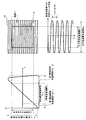
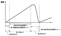
- FIG. 2 is a diagram for explaining characteristics of a vertical drive signal for driving a vertical scanning element of the vertical scanning unit shown in FIG. 1. It is a figure for demonstrating the fluctuation
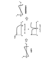
- FIG. 2 is a diagram for explaining a waveform of a vertical drive signal for driving a vertical scanning element of the vertical scanning unit shown in FIG. 1.
- FIG. 2 is a diagram for explaining a waveform of a vertical drive signal for driving a vertical scanning element of the vertical scanning unit shown in FIG. 1.
- FIG. 2 is a diagram for explaining a waveform of a vertical drive signal for driving a vertical scanning element of the vertical scanning unit shown in FIG. 1.
- FIG. 2 is a diagram for explaining a waveform of a vertical drive signal for driving a vertical scanning element of the vertical scanning unit shown in FIG. 1.
- FIG. 2 is a diagram for explaining a waveform of a vertical drive signal for driving a vertical scanning element of the vertical scanning unit shown in FIG. 1.
- FIG. 2 is a diagram for explaining a waveform of a vertical drive signal for driving a vertical scanning element of the vertical scanning unit shown in FIG. 1.
- FIG. 1 is a diagram for explaining a waveform of a vertical drive signal for driving a vertical scanning element of the vertical scanning unit shown in FIG. 1.
- FIG. 2 is a diagram for explaining a waveform of a vertical drive signal for driving a vertical scanning element of the vertical scanning unit shown in FIG. 1.
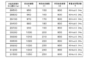
- FIG. 2 is a diagram for explaining a waveform of a vertical drive signal for driving a vertical scanning element of the vertical scanning unit shown in FIG. 1. It is explanatory drawing of the brightness
- the image display device includes a light source unit that emits light having an intensity corresponding to an image signal, a light scanning unit that performs two-dimensional scanning on the light emitted from the light source unit, and a control that controls the light source unit and the light scanning unit.
- the light scanned by the light scanning unit is directly projected onto the retina of at least one eye of the user who is an observer, and the image is projected to display the image.
- the present invention is not limited to such an image display device.
- an image projection device that displays light by scanning light scanned by a light scanning unit on a screen surface, light is scanned.
- the present invention can be applied to other image display devices that display images.
- the image display device 1 is an image display device that displays an image by two-dimensionally scanning light corresponding to the image signal S and directly projecting the light on the retina of a user who is an observer.
- the image display device 1 includes a display control unit 10, a light source unit 20, an optical scanning unit 40, and a relay optical system 50.
- the display control unit 10 controls each unit according to the input image signal S.
- the light source unit 20 emits light according to the image signal S under the control of the display control unit 10.
- the optical scanning unit 40 performs two-dimensional scanning on the light emitted from the light source unit 20.
- the relay optical system 50 also has a function as an eyepiece optical system that projects the light scanned by the light scanning unit 40 onto the user's eye 60.
- the light emitted from the light source unit 20 enters the optical scanning unit 40 through the optical fiber 30.
- the display control unit 10 receives an image signal S from the outside, and based on the image signal S, red (R), green (G), and blue (B) image signals 12R, 12G, An image signal supply circuit 11 for generating 12B, a control unit 13 for controlling the entire display control unit 10, and an image signal input I / F 14 for inputting an image signal S from the outside are provided.
- the light source unit 20 is provided with an R laser 24, a G laser 25, and a B laser 26, and an R laser driver 21, a G laser driver 22, and a B laser driver 23 for driving these lasers 24 to 26, respectively.
- a collimating optical system 27 provided so as to collimate the laser light emitted from each of the lasers 24 to 26 into parallel light, a dichroic mirror 28 for combining the collimated laser lights, and a combined laser.
- An optical system 29 that guides light to the optical fiber 30 is provided.
- semiconductor lasers such as laser diodes or solid-state lasers are used.
- the image signal supply circuit 11 of the display control unit 10 generates the image signals 12R, 12G, and 12B of the respective colors based on the image signal S as described above and inputs them to the laser drivers 21 to 23. Thereby, the light of the single color or the composite color of red (R), green (G), and blue (B) can be emitted from the light source unit 20.
- the laser light thus generated by the light source unit 20 and incident on the optical fiber 30 is light used for image formation.
- this laser light is referred to as “image light”.
- the optical scanning unit 40 includes a collimating optical system 41 for collimating the image light emitted from the optical fiber 30 and the collimated image light at a relatively high speed in the horizontal direction (first direction) that is the main scanning direction.
- a horizontal scanning section 42 that scans in the horizontal direction
- a relay optical system 43 that guides the image light scanned in the horizontal direction to a vertical scanning section 44 to be described later, and image light incident through the relay optical system 43 is substantially horizontal.
- a vertical scanning unit 44 that scans at a relatively low speed in the vertical direction (second direction) that is a sub-scanning direction that intersects perpendicularly.
- the image light scanned by the light scanning unit 40 in this way is incident on the pupil 61 of the user's eye 60 via the relay optical system 50.
- the image light is converted by the relay optical system 50 so that each scanned light beam is converged at the position of the pupil 61 of the user's eye 60.
- the horizontal scanning unit 42 is an optical system that horizontally scans image light in a horizontal direction for each horizontal scanning line of an image to be displayed.
- the horizontal scanning unit 42 includes an optical scanning element 42a (hereinafter referred to as a “high-speed scanning element 42a”) having a reflection mirror 42b that is oscillated by a drive signal, such as a galvano mirror, and the high-speed scanning element 42a. And a swing state detector 42d for detecting the swing state of the reflection mirror 42b of the high speed scanning element 42a.
- the high-speed scanning element 42a is a resonance type optical scanning element, and the reflection mirror 42b is oscillated and oscillated by inputting a drive signal having a resonance frequency that matches the resonance characteristic of the high-speed scanning element 42a.
- the swing state detector 42d detects the swing frequency of the reflection mirror 42b, the swing magnitude (amplitude) of the reflection mirror 42b, the phase difference between the horizontal drive signal 15 and the swing state, and the like.
- the state signal 45 is output to the control unit 13 of the display control unit 10.
- the swinging state detection unit 42d includes a beam light source and a light detector (beam detector).
- the swinging state detection unit 42d emits an inspection beam light from the beam light source to the reflection mirror 42b, and the reflection mirror 42b detects the reflected light by the reflection mirror 42b and the detection timing of the reflection mirror 42b. Detects swing magnitude, swing frequency and phase.
- the fluctuation of the beam member 42e is converted into an electrical signal, and the magnitude and frequency or phase of oscillation are changed. You may make it detect.
- the vertical scanning unit 44 is an optical system that vertically scans image light vertically from the first horizontal scanning line to the last horizontal scanning line for each frame of an image to be displayed.
- the vertical scanning unit 44 includes an optical scanning element 44a (hereinafter referred to as a “low speed scanning element 44a”) having a reflection mirror 44b that is oscillated by a drive signal, such as a galvano mirror, and the low speed scanning element 44a.
- a vertical drive circuit 44c an example of a low-speed scanning element driving unit.
- the low speed scanning element 44a tilts the reflection mirror 44b in a direction corresponding to the signal level of the input drive signal, and scans the incident light by the reflection mirror 44b in the vertical direction.
- the reflection mirror 44b of the low-speed scanning element 44a is swingably supported by a fixed member via an elastic beam member 44d.
- the low-speed scanning element has a specific resonance frequency that is determined by the material characteristics and the dimension / shape characteristics of the reflection mirror 44b and the beam member 44d.
- the “maximum scanning range” means the maximum range in which the high-speed scanning element 42 a of the horizontal scanning unit 42 and the low-speed scanning element 44 a of the vertical scanning unit 44 can scan image light.
- the horizontal drive circuit 42c amplifies the horizontal drive signal 15 output from the display control unit 10, applies it to the high-speed scanning element 42a, and drives the reflection mirror 42b of the high-speed scanning element 42a.
- the vertical drive circuit 44c amplifies the vertical drive signal 16 output from the display control unit 10, applies it to the low speed scanning element 44a, and forcibly drives the reflection mirror 44b of the low speed scanning element 44a. Then, the display control unit 10 starts from the light source unit 20 when the effective scanning range Z has the scanning positions of the high-speed scanning element 42a and the low-speed scanning element 44a in the maximum scanning range W of the high-speed scanning element 42a and the low-speed scanning element 44a.
- the intensity-modulated image light is emitted according to the image signal S.
- FIG. 2 virtually shows the locus ⁇ of the image light scanned by the high speed scanning element 42a and the low speed scanning element 44a when it is assumed that the image light is always emitted from the light source unit 20.
- the locus ⁇ of the image light is simply shown in FIG. 2 for ease of viewing.
- control unit 13 includes a CPU (Central Processing Unit) 100, first to third ROMs (Read Only Memory) 101 to 103, a RAM (Random Access Memory) 104, and a VRAM (VRAM) for storing image data to be displayed.
- the second and third ROMs 102 and 103 and the RAM 104 may be collectively referred to as the storage unit 110.
- the CPU 100, the first to third ROMs 101 to 103, the RAM 104, the VRAM 105, and the D / A converter 108 are connected to a data communication bus, and various information is transmitted via the data communication bus. Send and receive.
- the CPU 100 executes various functions as the control unit 13 by executing various information processing programs stored in the first ROM 101.
- the control unit 13 reflects as a drive signal generation unit from the swing state signal 45 including information such as the swing frequency, swing magnitude, and phase of the reflection mirror 42b input from the swing state detection unit 42d.
- a horizontal drive signal 15 having a frequency at which the mirror 42b resonates and oscillates (resonance frequency fr of the high-speed scanning element 42a) is generated, and the reflection mirror 42b of the high-speed scanning element 42a oscillates and resonates.
- the control unit 13 generates and outputs the vertical drive signal 16 based on the resonance frequency fr of the high-speed scanning element 42a detected by the swing state detection unit 42d as a drive signal generation unit.
- control unit 13 develops the image data of each pixel constituting the image corresponding to the image signal S input via the image signal input I / F 14 in the internal VRAM 105, and the horizontal drive signal 15 and the vertical drive signal 16. Is output to the image signal supply circuit 11 at a timing synchronized with the image signal.
- the image data is D / A converted by the image signal supply circuit 11 and output as image signals 12R, 12G, and 12B to the laser drivers 21 to 23 for the respective colors.
- the reflection mirror 44b of the low-speed scanning element 44a is swingably supported by the fixed member via the elastic beam member 44d, the reflection mirror 44b is inherently determined by the material characteristics, dimension and shape characteristics of the reflection mirror 44b and the beam member 44d. There is a resonant frequency. Therefore, if the vertical drive signal 16 includes a resonance frequency unique to the low speed scanning element 44a, the reflection mirror causes resonance vibration. Then, this resonance vibration superimposes a high-frequency component unnecessary for the swinging of the reflecting mirror, and a situation in which optical scanning cannot be performed properly occurs.
- the vertical drive signal 16 is a sawtooth waveform signal subjected to low pass filter processing and notch filter processing using a linearly changing sawtooth waveform signal as an original signal.
- the resonance characteristic inherent to the low-speed scanning element 44a is that the primary resonance frequency is f1 [Hz] and the secondary or higher resonance frequency is f2 [Hz] or more.
- the low-pass filter processing for attenuating the frequency of f2 (> f1) [Hz] or higher is applied to the sawtooth waveform signal, thereby suppressing the influence of the secondary or higher resonance among the resonance characteristics unique to the low-speed scanning element 44a.
- the a notch filter process that attenuates around the frequency of f1 [Hz] to the sawtooth waveform signal the influence of the primary resonance among the resonance characteristics unique to the low-speed scanning element 44a is suppressed.
- the sawtooth waveform signal obtained by performing low-pass filter processing and notch filter processing on the linearly changing sawtooth waveform signal is used as the vertical drive signal 16, so that the resonance frequency unique to the low-speed scanning element 44 a in the vertical drive signal 16.
- the component is reduced, and the resonance vibration of the reflection mirror 44b is suppressed. This avoids a situation in which high-frequency components are superimposed on the swing of the reflection mirror due to the resonance vibration, and the optical scanning cannot be performed appropriately.
- the resolution of the display image is 800 ⁇ 600 pixels
- the design value of the resonance frequency fr of the high-speed scanning element 42a is 30 kHz (note that the horizontal scanning frequency is reciprocating scanning, so the design value of the horizontal scanning frequency is doubled to 60 kHz.
- the design value of the vertical scanning frequency f1 is 60 Hz
- the number of times the reflecting mirror 44b of the high-speed scanning element 42a swings in the horizontal direction per vertical scanning period Tv (see FIG. 2) of the low-speed scanning element 44a in other words It is assumed that the design value of the number of scanning lines (hereinafter referred to as “total number of scanning lines N”) that can be formed by the high-speed scanning element 42a per one vertical scanning period Tv is 1000. Further, it is assumed that the image size of the display image is substantially constant, and the variation in the resonance frequency fr of the high-speed scanning element 42a is ⁇ 5% (30 kHz ⁇ 1500 Hz).
- the invalid scanning line number n1 is a value obtained by subtracting the scanning number (hereinafter referred to as “effective scanning line number n2”) from which the high-speed scanning element 42a actually scans image light from the total scanning line number N.
- the effective scanning line number n2 is 800 because the resolution of the display image is 800 ⁇ 600 pixels.
- the vertical scanning frequency fl of the low-speed scanning element 44a can be suppressed to within ⁇ 0.5% (60 ⁇ 0.3 Hz).
- the frequency of the vertical drive signal 16 (vertical scanning frequency fl) is substantially constant, and one vertical scanning period Tv is substantially constant.
- the resonance frequency fr of the high-speed scanning element 42a is high, the number of invalid scanning lines n1 increases, and the vertical drive signal 16 having a waveform that shortens one vertical effective scanning period Tv1 as shown in FIG. 6A is required. Further, when the resonance frequency fr of the high-speed scanning element 42a is low, the number of invalid scanning lines n1 decreases, and the vertical drive signal 16 having a waveform that increases one vertical effective scanning period Tv1 as shown in FIG. 6B is required.
- the inclination range of the high-speed scanning element 42a is made substantially constant (the range of amplitudes a to b in FIGS. 6A and 6B).
- the number of invalid scanning lines n1 is changed in units of one unit (10 horizontal scanning units) for fluctuations of about ⁇ 1% of the resonance frequency fr.
- the fluctuation of fr is changed by about 0.1% by changing the number of invalid scanning lines n1 in one unit (one horizontal scanning unit), and the number of invalid scanning lines n1 is increased or decreased by one unit.
- the fluctuation of the oscillation period (low-speed scanning period) of the low-speed scanning element due to the fluctuation of the resonance frequency of the high-speed scanning element is reduced within the time of one scanning period by the high-speed scanning element 42a, that is, the oscillation period of the high-speed scanning element 42a.
- the fluctuation can be within 1/2 time (1 / fh) of the period (1 / fr shown in FIG. 2), and fluctuation of the oscillation cycle of the low-speed scanning element can be minimized.
- the vertical scanning frequency of the low speed scanning element 44a can be defined by the number of horizontal scanning lines by the high speed scanning element 42a.
- the period of the vertical drive signal 16 is made substantially constant by changing the waveform of the vertical drive signal 16 in accordance with the resonance frequency fr of the high-speed scanning element 42a.
- the waveform data of the plurality of vertical drive signals 16 is stored in the second and third ROMs 102 and 103. Hereinafter, this point will be specifically described.
- the control unit 13 divides the sawtooth waveform data for generating the vertical drive signal 16 into the first waveform data and the second waveform data and stores them in the second and third ROMs 102 and 103. The points to be described will be described.
- the data of the vertical drive signal 16 is obtained by dividing the sawtooth waveform of the vertical drive signal 16 for one cycle (one vertical scanning period Tv) into a first waveform W1 and second waveforms W2, W2 ′, and storing means 110 (first 2 and third ROMs 102 and 103).
- the first waveform W1 is a waveform for scanning light in the sawtooth waveform of the vertical drive signal 16 for one cycle, and the vertical drive signal 16 during the vertical effective scanning period Tv1. It is a waveform.
- the second waveforms W2 and W2 ′ are waveforms excluding the first waveform W1 from the sawtooth waveform of the vertical drive signal 16 for one cycle.
- the waveform of the vertical drive signal 16 during the first vertical invalid scanning period Tv2-1 is the second waveform W2
- the waveform of the vertical drive signal 16 during the second vertical invalid scanning period Tv2-2 is the second waveform W2 ′.
- the second ROM 102 stores data of the first waveform W1
- the third ROM 103 stores data of the second waveforms W2 and W2 ′.
- the CPU 100 reads the data of the first waveform W1 and the data of the second waveforms W2 and W2 ′ from the second and third ROMs 102 and 103, generates drive signal data using these data, and stores them in the RAM 104. Then, the CPU 100 generates the vertical drive signal 16 for one cycle by converting the drive signal data stored in the RAM 104 into an analog signal by the D / A converter 108 (see FIG. 1). A vertical drive signal 16 having a continuous sawtooth waveform is generated as shown in FIG.
- the first waveform W1 stored in the second ROM 102 in the storage unit 110 is one type. In order to make the size of the display image substantially constant, it is necessary to change the slope of the first waveform W1 portion of the vertical drive signal 16 in accordance with the resonance frequency fr of the high-speed scanning element 42a.
- the first waveform W1 (see FIG. 9B) when the resonance frequency fr of the high-speed scanning element 42a is 31500 Hz is steeper than the first waveform W1 when the design value is 30000 Hz (see FIG. 9A)
- the first waveform W1 (see FIG. 9C) when the resonance frequency fr of the high-speed scanning element 42a is 28800 Hz needs to have a gentler slope than the first waveform W1 (see FIG. 9A) when the design value is 30000 Hz. is there.
- the slope of the first waveform W1 portion of the vertical drive signal 16 is changed in accordance with the resonance frequency fr of the high-speed scanning element 42a.
- the data is sequentially read from the second ROM 102, and all the data of the first waveform W1 is read in 8/600 seconds.
- the resonance frequency fr of the high-speed scanning element 42a is 31500 Hz
- the slope of the first waveform W1 portion of the vertical drive signal 16 becomes steeper than when the resonance frequency fr of the high-speed scanning element 42a is 30000 Hz.
- the resonance frequency fr of the high-speed scanning element 42a is 28800 Hz
- the period of the first waveform W1 portion of the vertical drive signal 16 changes according to the resonance frequency fr of the high-speed scanning element 42a, while the period of the vertical drive signal 16 is suppressed to 1/60 seconds ⁇ 0.5%. Therefore, it is necessary to change the period of the second waveform W2, W2 ′ portion of the drive signal in accordance with the resonance frequency fr of the high-speed scanning element 42a.
- the period of the second waveforms W2, W2 ′ of the vertical drive signal 16 is changed, and the vertical drive signal 16 It is also conceivable to change the period to 1/60 seconds ⁇ 0.5%.
- the low-speed scanning element 44a has a specific resonance frequency, and the vertical drive signal 16 must suppress the resonance frequency component of the low-speed scanning element 44a. If the read timing of the second waveforms W2, W2 ′ is simply changed, the frequency component of the vertical drive signal 16 changes, and the resonance frequency component of the low-speed scanning element 44a may not be suppressed.
- a plurality of types of second waveforms W2-1, W2′-1 to W2-n, W2′-n (n is an integer equal to or greater than 2.
- n 11) according to the resonance frequency fr of the high-speed scanning element 42a.
- the third ROM 103 in the storage means 110 stores a second waveform table shown in FIG.
- This second waveform table is a table in which the resonance frequency fr of the high-speed scanning element 42a is associated with the data names of the second waveforms W2-1, W2′-1 to W2-11, W2′-11 in units of 300 Hz. .
- the CPU 100 determines the data names of the second waveforms W2 and W2 ′ corresponding to the resonance frequency fr of the high-speed scanning element 42a notified from the swing state detection unit 42d using the second waveform table, and determines the determined second waveform W2. , W2 ′, the data of the second waveform W2, W2 ′ corresponding to the data name is read from the third ROM 103.
- the reading from the third ROM 103 is performed at a timing continuous with the timing of reading the first waveform W1.
- the first waveform W1 and the second waveforms W2, W2 ′ are changed to the second.
- the present invention is not limited to this.
- the first waveform W1 and the second waveforms W2, W2 ′ are not stored in the RAM 104, but the first waveform W1 and the second waveforms W2, W2 ′ are read directly from the second and third ROMs 102, 103.
- the D / A converter 108 may convert the signal into an analog signal.
- the second waveforms W2 and W2 ′ have been described separately as two waveforms. However, these second waveforms W2 and W2 ′ are continuous (see FIG. 8), and one waveform W2 ′′ (W2 + W2 ′). May be stored in the third ROM 103. Also, the first waveform W1 and the second waveforms W2, W2 ′ are stored in the third ROM 103 as one waveform and read out as separate waveforms by address control or the like when read. It may be configured to read out, or of course, a plurality of first waveforms may be stored.
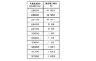
- control unit 13 stores a luminance table in which the resonance frequency of the high-speed scanning element and the luminance correction ratio Kj are associated with each other in the third ROM 103.
- this luminance table associates the resonance frequency of the high-speed scanning element 42a with the luminance correction ratio Kj at intervals of 300 Hz. Therefore, the CPU 100 changes the luminance information of the image signal output to the image signal supply circuit 11 by referring to the LUT, changing the luminance correction ratio Kj according to the resonance frequency fr of the high-speed scanning element. For example, when the resonance frequency fr of the high-speed scanning element 42a is 28500 Hz, the CPU 100 increases the intensity of each luminance signal of the image signal by 0.952 times and outputs it to the image signal supply circuit 11. When the swing range of the high-speed scanning element 42a changes according to the resonance frequency, it is necessary to adjust the change.
- the luminance of the light corresponding to the image signal is changed according to the resonance frequency of the high-speed scanning element 42a, so that the luminance of the image to be displayed is suppressed from changing according to the resonance frequency. Can be maintained.
- the CPU 100 inputs a predetermined horizontal drive signal 15 (for example, 30000 Hz horizontal drive signal 15) to the high-speed scanning element 42a.
- the high speed scanning element 42a starts swinging the reflection mirror 42b (step S10).
- the CPU 100 acquires information such as the swing frequency, swing magnitude, and phase difference of the reflection mirror 42b of the high-speed scanning element 42a from the swing state detection unit 42d, and determines the frequency and amplitude of the horizontal drive signal 15. Change (step S11).
- the CPU 100 determines whether or not the high-speed scanning element 42a is in a resonance state (step S12). At this time, the CPU 100 determines that the high-speed scanning element 42a is in a resonance state when the magnitude of the swing of the reflection mirror 42b of the high-speed scanning element 42a and the phase difference between the horizontal drive signal 15 and the swinging state are within a predetermined range. If the magnitude or phase difference of the reflection mirror 42b of the high-speed scanning element 42a is outside a predetermined range, it is determined that the high-speed scanning element 42a is not in a resonance state.
- step S12 If it is determined that the high speed scanning element 42a is not in the resonance state (step S12: No), the CPU 100 returns to the process of step S11 again in order to wait for the high speed scanning element 42a to be in the resonance state. If the resonance does not occur after a predetermined time, the driving of the high speed scanning element 42a is stopped.
- step S12 if it is determined that the high-speed scanning element 42a is in a resonance state (step S12: Yes), the CPU 100 detects the resonance frequency of the high-speed scanning element 42a (step S12). That is, the frequency of the horizontal drive signal 15 input to the high-speed scanning element 42a in the resonance state is set as the resonance frequency of the high-speed scanning element 42a. And CPU100 memorize
- the CPU 100 determines whether or not the resonance frequency value (memory value) stored in step S14 this time is the same as the resonance frequency value (memory value) stored in the previous step S14 (step S15).
- the initial value of the resonance frequency value (stored value) stored in the RAM 104 is 30000 Hz. Therefore, when the process of step S15 is first performed, it is determined whether or not the initial value and the current stored value are the same value.
- step S15: No the CPU 100 reads the first waveform W1 from the second ROM 102, and stores the current stored value (resonance of the high-speed scanning element 42a).
- the second waveforms W2, W2 ′ corresponding to the frequency) are selected from the third ROM 103 and read out.
- the read second waveform W2, first waveform W1, and second waveform W2 ′ are connected to generate drive signal data and store it in the RAM 104 (step S16).
- step S15: Yes the CPU 100 does not perform the process of step S16.
- the CPU 100 generates the vertical drive signal 16 (step S17). That is, the CPU 100 sequentially reads the drive signal data stored in the RAM 104 with a read clock signal having a cycle determined based on the resonance frequency of the high-speed scanning element 42a, and inputs the drive signal data to the D / A converter 108 to output the vertical drive signal 16. Generate and output. Note that the first waveform W1 and the second waveforms W2, W2 ′ can also be read directly from the second and third ROMs 102, 103 without storing the drive signal data in the RAM 104. In this case, the CPU 100 selects the second waveforms W2 and W2 ′ corresponding to the current stored value (resonance frequency of the high speed scanning element 42a) in step S16.
- each data is a read clock signal having a cycle determined based on the resonance frequency of the high-speed scanning element 42a. read out.
- the CPU 100 inputs the read clock signal to the D / A converter 108 and causes the D / A converter 108 to output the vertical drive signal 16.
- step S1 The above processing is continued until a driving end instruction or a pause instruction is issued by the user (step S1).
- the CPU 100 acquires information on the resonance frequency fr of the high-speed scanning element 42a from the oscillation state detection unit 42d, and stores it by a read clock signal having a period determined based on the resonance frequency.
- the data of the first waveform W1 stored in 110 is sequentially read.
- the CPU 100 generates the vertical drive signal 16 for the first waveform W1 by inputting the data read in this way to the D / A converter 108.
- the CPU 100 selects a sawtooth shape from the data of the second waveforms W2-1, W2′-1 to W2-11, W2′11 stored in the storage unit 110 according to the resonance frequency of the high-speed scanning element 42a.
- Data of the second waveforms W2 and W2 ′ for maintaining the fluctuation of the waveform cycle within a predetermined time are sequentially read out from the storage means 110 at the read timing of the cycle according to the resonance frequency of the high-speed scanning element 42a, and the D / A converter. To generate the vertical drive signal 16 of the second waveform portion.
- the frequency can be made substantially constant, and the oscillation state of the low-speed scanning element 44a can be easily stabilized.
- the second waveforms W2 and W2 ′ are waveforms in which the component of the resonance frequency unique to the low speed scanning element 44a is suppressed, it is possible to suppress the induction of the resonance vibration of the reflection mirror 44b of the low speed scanning element 44a.
- the low-speed scanning element 44a in which the reflection mirror 44b is swingably supported by the fixed member via the elastic beam member 44d has been described as an example.
- the present invention is not limited to this configuration, and any low-speed scanning element having a specific resonance frequency can be applied.
- an example of solving the problem of the natural resonance of the low-speed scanning element has been given, but this is given as the most effective example.
- the waveform stored in the storage means is not a waveform that suppresses natural resonance, the gist of the present invention is not different.
- the embodiment of the present invention naturally includes a case in which the fluctuation of the driving frequency (sub-scanning frequency) of the low-speed scanning element caused by the fluctuation of the frequency of the high-speed scanning element can be suppressed within a certain range.
- a plurality of types of second waveform data are stored in the storage unit according to the resonance frequency of the high-speed scanning element, and the second waveform data of a type corresponding to the resonance frequency of the high-speed scanning element is stored.
- An example in which the drive signal of the second waveform portion is generated by reading from the storage means has been described.
- the present invention is not limited to this, and the second waveform data is sequentially read at the read timing corresponding to the resonance frequency according to the resonance frequency of the high-speed scanning element, and the drive signal of the second waveform portion corresponding to the resonance frequency of the high-speed scanning element. As long as it generates For example, only one type of the second waveform may be stored in the storage unit.
- data of the second waveform when the resonance frequency of the high-speed scanning element is the highest (preparing the data with the largest number of data, in other words, the waveform having the longest period) is prepared, and according to the resonance frequency of the high-speed scanning element
- the read address of the data and the number of data are changed.
- storage means can be reduced.
- the waveform of the vertical effective scanning period Tv1 in the vertical drive signal 16 is the first waveform
- the waveform of the vertical invalid scanning period Tv2-1 and Tv2-2 is the second waveform.
- the first waveform includes the waveform of the portion of the vertical effective scanning period Tv1, and does not necessarily have to be exactly the same as the portion of the vertical effective scanning period Tv1.
- the resolution of the display image is 800 ⁇ 600 pixels
- the design value of the resonance frequency of the high-speed scanning element 42 a is 30 kHz
- the total number of scanning lines N is 1000
- the resonance frequency of the high-speed scanning element 42 a varies.
- the (variation) is ⁇ 5% (30 kHz ⁇ 1500 Hz)
- the variation of about 1% (300 Hz) of the resonance frequency fr is one unit, but this is for the purpose of briefly explaining the present invention. Needless to say, it is not limited.
- the sawtooth waveform signal has been described by taking the waveform signal as shown in FIG. 3 as an example. However, if it is a periodic waveform including a substantially straight line portion for scanning light, For example, it may be a triangular wave, a trapezoidal wave, a sine wave, or the like.
Landscapes
- Physics & Mathematics (AREA)
- Engineering & Computer Science (AREA)
- General Physics & Mathematics (AREA)
- Optics & Photonics (AREA)
- Multimedia (AREA)
- Signal Processing (AREA)
- Computer Hardware Design (AREA)
- Theoretical Computer Science (AREA)
- Mechanical Optical Scanning Systems (AREA)
- Control Of Indicators Other Than Cathode Ray Tubes (AREA)
Abstract
駆動信号の鋸歯形状波形のうち光を走査するための第1波形W1のデータを記憶すると共に、前記鋸歯形状波形のうち第1波形W1を除く第2波形W2,W2'のデータを記憶する記憶手段を備え、高速走査素子の共振周波数に応じた周期の読み出しタイミングで前記記憶手段から第1波形W1のデータを順次読み出して第1波形W1部分の駆動信号を生成し、さらに高速走査素子の共振周波数に応じて前記記憶手段に記憶した複数の第2波形W2,W2'のデータを順次読み出して高速走査素子の共振周波数に応じた第2波形W2,W2'部分の駆動信号を生成して、前記鋸歯形状波形の周期の変動を所定時間以内に維持する。
Description
本発明は、画像信号に応じた光を2次元走査して画像を表示する画像表示装置に関する。
従来から、画像信号に基づいて生成した光(以下、「画像光」と呼ぶ。)をガルバノミラーなどの光走査素子を用いて2次元走査し、画像を表示する光走査型の画像表示装置が知られている。
この種の画像表示装置は、一般的に、高速走査を行う光走査素子(以下、「高速走査素子」と呼ぶ。)の反射ミラーで画像光を水平方向に走査し、次いで、その水平走査された画像光を低速走査を行う光走査素子(以下、「低速走査素子」と呼ぶ。)の反射ミラーで垂直方向に走査することにより、2次元走査された画像を表示する。
例えば、特許文献1には、共振型の高速走査素子(主走査素子)の反射ミラーをその共振周波数frで共振揺動させて画像光を水平方向に走査し、その水平方向に走査された画像光を、低速走査素子(副走査素子)の反射ミラーを鋸波形状波形の駆動信号で強制的に揺動させることにより垂直方向に走査してその結果2次元走査された画像を形成するという画像表示装置が開示されている。
高速走査素子の共振周波数frは、個体差(個々の構造のバラツキ)や温度等の環境特性によって設計値からずれるものが多い。このように高速走査素子の共振周波数frには個体差などのバラツキが存在するものの、安定した画像表示を行うには、低速走査素子の反射ミラーの駆動周波数を高速走査素子の共振周波数frと同期させる必要がある。
ところが、低速走査素子の反射ミラーの駆動周期を高速走査素子の共振周波数frに基づいて生成すると、高速走査素子の共振周波数frの変化に伴って低速走査素子の走査周期がずれる。例えば、高速走査素子の共振周波数frが10%高くなると、高速走査素子に対して同期駆動される低速走査素子の駆動周波数(走査周波数)も10%高くなることになる。外部機器などから供給される画像信号はその垂直同期周波数(フレーム周波数)が予め決まっている(一般に30フレーム/秒や60フレーム/秒)ことから、低速走査素子の駆動周波数が、垂直同期周波数と異なる場合は、その画像の特定のフレームを削除したり、2度同じフレームを再生したりしてフレーム数を補正する必要がある。そして、そのずれが大きいほど単位時間当たりの補正回数が増え、画像が時間方向に不連続な部分が目立つようになる。このことは、特に、画像の動き(変化)の激しい部分では顕著となる。
そこで、下記特許文献1に記載の装置では、高速走査素子の一走査周期に有効走査線数を積算した期間を、画像光を有効に走査する有効走査期間とし、低速走査素子の駆動周期から有効走査期間を減算した期間を、画像光を有効に走査しない無効走査期間として低速走査素子の反射ミラーの駆動周期(フレーム周期)を一定にしている。
しかしながら、上記特許文献1に記載の技術は、ステップモータで低速走査素子の反射ミラーを駆動するものであり、クロック信号に応じて反射ミラーを所定量だけ順次駆動させることは容易にできるものの、走査線数が多く高速な動作には脱調などが起きやすい等の問題があって向かない。高速な動作をさせる場合には電磁式の光走査素子が採用されることが多いが、電磁式の光走査素子は鋸波形状の駆動波形を形成し、それを駆動信号として駆動するため、特許文献1に記載のステップモータを使った技術等は適用することができない。
しかも、単に無効走査期間を変更しただけでは光走査を適切に行なうことができないことがある。
例えば、反射ミラーを弾性のある梁部材を介して固定部材に揺動可能に支持した走査素子を低速走査素子とした場合、この低速走査素子には反射ミラー及び梁部材の特性で決まる固有の共振周波数が存在する。そのため、このような走査素子を低速走査素子として用いる場合、この低速走査素子を駆動する駆動信号に低速走査素子固有の共振周波数が含まれていると、反射ミラーの共振振動が誘起される。そして、この共振振動により反射ミラーの揺動に不要な周波成分の揺動が重畳してしまい、駆動信号に忠実な光走査が実現できない事態が生じる。
そこで、本発明は、共振周波数が変化する高速走査素子と固有の共振周波数を有する低速走査素子とを用いた画像表示装置において、低速走査素子の揺動周期を安定させ、さらに、低速走査素子の反射ミラーの共振振動が誘起されることを抑制することを目的とする。
上記目的を達成するために、本発明の一つの観点によれば、画像信号に応じた強度の光を2次元走査して画像を表示する画像表示装置において、前記画像信号に応じた強度の光を出射する光源部と、共振揺動する反射ミラーにより入射した光を第1方向に相対的に高速に走査する共振型の高速走査素子と、入力される駆動信号の信号レベルに応じた方向に反射ミラーを傾斜させ、当該反射ミラーにより入射した光を前記第1方向と略直交する第2方向に相対的に低速に走査する低速走査素子と、前記高速走査素子の共振周波数を検出する検出部と、前記高速走査素子の共振周波数に応じた鋸歯形状波形の駆動信号を生成する駆動信号生成部と、前記駆動信号生成部で生成した前記駆動信号を前記低速走査素子に入力する低速走査素子駆動部と、を備える。前記駆動信号生成部は、記駆動信号の鋸歯形状波形のうち光を有効走査するための第1波形のデータを記憶すると共に、前記駆動信号の鋸歯形状波形のうち第1波形を除く波形である第2波形のデータを記憶する記憶手段を備え、前記高速走査素子の共振周波数に応じた読み出しタイミングで前記記憶手段に記憶した第1波形のデータを順次読み出して前記第1波形部分の前記駆動信号を生成し、前記高速走査素子の共振周波数に応じて前記第2波形のデータを前記読み出しタイミングで順次読み出して前記高速走査素子の共振周波数に応じた前記第2波形部分の前記駆動信号を生成することにより、前記鋸歯形状波形の周期の変動を所定時間以内に維持するものである。
このような構成にすることにより、高速走査素子の共振周波数の変動に応じて発生する、低速走査素子の揺動周期(低速走査周期)の変動を最小限に抑えることができる。また、例えば、第2波形を低速走査素子固有の共振周波数の成分を抑圧した波形とすることにより、低速走査素子の反射ミラーの共振振動が誘起されることを抑制することができる。
また、画像表示装置において、前記駆動信号生成部は、前記読み出しタイミングで読み出す前記第1波形部分のデータの総数は一定とする一方、前記読み出しタイミングで読み出す前記第2波形部分のデータの総数は前記高速走査素子の共振周波数に応じて変化させることができる。
このような構成にすることにより、鋸歯形状波形の周期変動を所定の範囲内に維持することが容易となる。
また、画像表示装置において、前記記憶手段に、前記高速走査素子の共振周波数に応じて複数種類の前記第2波形のデータを記憶すると共に、前記駆動信号生成部は、前記高速走査素子の共振周波数に応じた種類の前記第2波形のデータを前記記憶手段から読み出して前記第2波形部分の前記駆動信号を生成することができる。
このような構成にすることにより、例えば、第2波形のデータを1種類とし、そのデータの一部を選択して抽出することに比べ、データの選択処理に伴う負荷を軽減することができる。また、データの一部を選択して抽出することに比べ、自由度が高く、第2波形部分を低速走査素子固有の共振周波数の成分を抑圧した波形とすることが容易になる。
また、画像表示装置において、前記読み出しタイミングの周期は、前記高速走査素子の揺動周期の1/2の時間又はその整数倍であって、前記駆動信号の周波数帯域を抑圧しない周期とすることができる。
このような構成にすることにより、低速走査素子の駆動信号の生成を、高速走査素子の走査周波数との同期を保ちつつ容易にでき、しかも、読み出しタイミングの周期を駆動信号の周波数帯域を抑圧しない周期としたので、低速走査素子を駆動する駆動信号を精度よく再現することができる。
また、画像表示装置において、前記所定時間は、前記高速走査素子による1走査の周期の時間とすることができる。
このような構成にすることにより、高速走査素子の共振周波数の変動による低速走査素子の揺動周期(低速走査周期)の変動を最も低減できる。
また、画像表示装置において、前記光源部は、前記画像信号に応じた光の輝度を前記高速走査素子の共振周波数に応じて変化させて、共振周波数に応じて表示する画像の輝度が変化するのを抑制することができる。
このような構成にすることにより、表示する画像の品質を向上させることができる。
本発明によれば、低速走査素子の揺動周期(低速走査周期)を安定させることができる。また、例えば、第2波形を低速走査素子固有の共振周波数の成分を抑圧した波形とすることにより、低速走査素子の反射ミラーの共振振動が誘起されることを抑制することができる。
以下に、本発明に好適な実施形態について図面に基づいて説明する。なお、以下の説明では、網膜走査型の画像表示装置を主に説明する。この画像表示装置は、画像信号に応じた強度の光を出射する光源部と、この光源部から出射された光を2次元走査する光走査部と、光源部と光走査部とを制御する制御部とを備える。そして、光走査部により走査した光を観察者である利用者の少なくとも一方の眼の網膜上に直接投射し、画像を投影して、画像を表示するものである。しかし、本発明は、このような画像表示装置に限定されるものではなく、例えば、光走査部により走査した光をスクリーン面に投影して、画像を表示する画像投影装置のほか、光を走査して画像を表示する他の画像表示装置に対して適用することができる。
(画像表示装置の構成)
まず、図1を参照して、本実施形態の網膜走査型の画像表示装置の構成を説明する。
まず、図1を参照して、本実施形態の網膜走査型の画像表示装置の構成を説明する。
本実施形態にかかる画像表示装置1は、画像信号Sに応じた光を2次元走査して観察者である利用者の網膜上に直接投射し、画像を表示する画像表示装置である。画像表示装置1は、図1に示すように、表示制御部10と、光源部20と、光走査部40と、リレー光学系50とを備えている。表示制御部10は、入力される画像信号Sに応じて各部を制御する。光源部20は、表示制御部10の制御により画像信号Sに応じた光を出射する。光走査部40は、光源部20から出射された光を2次元走査する。リレー光学系50は、光走査部40で走査された光を利用者の眼60に投射する接眼光学系としての機能も有する。なお、光源部20から出射された光は光ファイバ30を介して光走査部40に入射される。
表示制御部10には、外部からの画像信号Sが入力され、それに基づいて映像を合成するための要素となる赤(R),緑(G),青(B)の画像信号12R、12G、12Bを発生する画像信号供給回路11と、表示制御部10全体を制御する制御部13と、外部からの画像信号Sを入力する画像信号入力I/F14とが設けられている。
光源部20は、Rレーザ24,Gレーザ25,Bレーザ26と、これらのレーザ24~26をそれぞれ駆動するためのRレーザドライバ21,Gレーザドライバ22,Bレーザドライバ23とが設けられている。さらに、各レーザ24~26より出射されたレーザ光を平行光にコリメートするように設けられたコリメート光学系27と、それぞれコリメートされたレーザ光を合波するダイクロイックミラー28と、合波されたレーザ光を光ファイバ30に導く光学系29とが設けられている。なお、レーザ24~26として、レーザダイオード等の半導体レーザや固体レーザが用いられる。表示制御部10の画像信号供給回路11は、上述のように画像信号Sに基づいて各色の画像信号12R、12G、12Bを生成し、各レーザドライバ21~23へ入力する。これにより、光源部20から赤(R),緑(G),青(B)の各単色又は複合色の光を出射することができる。ここで、このように光源部20で生成され光ファイバ30に入射されるレーザ光は、画像形成に用いられる光であり、以下、このレーザ光を「画像光」と呼ぶ。
光源部20から光ファイバ30に導かれた画像光は光走査部40に入射される。この光走査部40には、光ファイバ30から出射された画像光をコリメートするコリメート光学系41と、このコリメートされた画像光を主走査方向である水平方向(第1方向)に相対的に高速に走査する水平走査部42と、この水平方向に走査された画像光を後述の垂直走査部44に導くリレー光学系43と、リレー光学系43を介して入射された画像光を水平方向と略垂直に交差する副走査方向である垂直方向(第2方向)に相対的に低速に走査する垂直走査部44とを有している。そして、このように光走査部40で走査された画像光は、リレー光学系50を介してユーザの眼60の瞳孔61に入射される。なお、リレー光学系50により画像光はユーザの眼60の瞳孔61の位置において各走査された光束が収束されるように変換される。
ここで、水平走査部42は、表示すべき画像の1水平走査線ごとに、画像光を水平方向に往復で水平走査する光学系である。そして、この水平走査部42には、ガルバノミラーなどの、駆動信号により揺動する反射ミラー42bを有する光走査素子42a(以下、「高速走査素子42a」と呼ぶ。)と、この高速走査素子42aを駆動する水平駆動回路42cと、高速走査素子42aの反射ミラー42bの揺動状態を検出する揺動状態検出部42dとを備えている。高速走査素子42aは共振型の光走査素子であり、高速走査素子42aの共振特性と一致する共振周波数の駆動信号を入力することにより反射ミラー42bが共振揺動する。また、揺動状態検出部42dは、反射ミラー42bの揺動周波数、反射ミラー42bの揺動の大きさ(振幅)、水平駆動信号15と揺動状態との位相差などを検出して揺動状態信号45として表示制御部10の制御部13へ出力する。なお、揺動状態検出部42dは、ビーム光源と光検知器(ビームディテクタ)とを有している。揺動状態検出部42dは、ビーム光源から反射ミラー42bに対して検査用のビーム光を出射し、この反射ミラー42bによる反射光の光検知器での検知状態及び検出タイミングにより、反射ミラー42bの揺動の大きさ、揺動周波数及び位相を検出する。なお、光走査素子42aの反射ミラー42bを支持する梁部材42eに圧電素子等を設けることにより、その梁部材42eの変動を電気信号に変換して揺動の大きさ及び揺動周波数又は位相を検出するようにしてもよい。
また、垂直走査部44は、表示すべき画像の1フレームごとに、画像光を最初の水平走査線から最後の水平走査線に向かって垂直に垂直走査する光学系である。そして、この垂直走査部44には、ガルバノミラーなどの、駆動信号により揺動する反射ミラー44bを有する光走査素子44a(以下、「低速走査素子44a」と呼ぶ。)と、この低速走査素子44aを駆動する垂直駆動回路44c(低速走査素子駆動部の一例)を備えている。低速走査素子44aは入力される駆動信号の信号レベルに応じた方向に反射ミラー44bを傾斜させ、当該反射ミラー44bにより入射した光を垂直方向に走査する。また、この低速走査素子44aの反射ミラー44bは弾性のある梁部材44dを介して固定部材に揺動可能に支持されている。なお、該低速走査素子には、反射ミラー44b及び梁部材44dの材料特性や寸法・形状特性で決まる固有の共振周波数が存在する。
図2には、水平走査部42の高速走査素子42a及び垂直走査部44の低速走査素子44aによる最大走査範囲W(図2に示す水平最大走査範囲Xa及び垂直最大走査範囲Yaにより形成される範囲)と有効走査範囲Z(図2に示す水平有効走査範囲X1及び垂直有効走査範囲Y1により形成される範囲)との関係が示されている。ここで、「最大走査範囲」とは、水平走査部42の高速走査素子42a及び垂直走査部44の低速走査素子44aが画像光を走査できる最大の範囲を意味する。
水平駆動回路42cは、表示制御部10から出力される水平駆動信号15を増幅して、高速走査素子42aに印加し、高速走査素子42aの反射ミラー42bを駆動する。垂直駆動回路44cは、表示制御部10から出力される垂直駆動信号16を増幅して、低速走査素子44aに印加し、低速走査素子44aの反射ミラー44bを強制駆動する。そして、表示制御部10は、高速走査素子42a及び低速走査素子44aの最大走査範囲Wのうち、有効走査範囲Zに高速走査素子42a及び低速走査素子44aの走査位置がある場合に光源部20から画像信号Sに応じて強度変調された画像光を出射させる。これにより、高速走査素子42a及び低速走査素子44aによって画像光が有効走査範囲Zで走査され、1フレーム分の画像光が有効走査範囲Z内で走査される。この走査が1フレームの画像ごとに繰り返される。なお、図2には、光源部20から画像光が常時出射されたと仮定したときに高速走査素子42a及び低速走査素子44aによって走査される画像光の軌跡γが仮想的に示されている。ただし、高速走査素子42aによる水平走査方向Xの水平走査線数は、1フレームあたり数百又は千程度あるので、図2では見やすさのため画像光の軌跡γを簡略して記載している。
また、制御部13は、CPU(Central Processing Unit)100、第1~第3のROM(Read Only Memory)101~103、RAM(Random Access Memory)104、表示させる画像データを記憶しておくVRAM(Video Random Access Memory)105、デジタルアナログ変換器(D/A変換器)108を備えている。なお、以下においては、第2及び第3のROM102,103及びRAM104を含めて記憶手段110と呼ぶ場合がある。
そして、これらCPU100、第1~第3のROM101~103、RAM104、VRAM105,D/A変換器108は、データ通信用のバスにそれぞれ接続されており、このデータ通信用のバスを介して各種情報の送受信を行う。
CPU100は、第1のROM101に記憶されている各種情報処理プログラムを実行することにより、制御部13としての各種機能を実行する。例えば、制御部13は、駆動信号生成部として、揺動状態検出部42dから入力される反射ミラー42bの揺動周波数、揺動の大きさ、位相などの情報を含む揺動状態信号45から反射ミラー42bが共振振動する周波数(高速走査素子42aの共振周波数fr)の水平駆動信号15を生成して、高速走査素子42aの反射ミラー42bを共振振動させる。また、制御部13は、駆動信号生成部として揺動状態検出部42dで検出される高速走査素子42aの共振周波数frに基づいて垂直駆動信号16を生成して出力する。また、制御部13は、画像信号入力I/F14を介して入力した画像信号Sに対応する画像を構成する各画素の画像データを内部のVRAM105に展開し、水平駆動信号15や垂直駆動信号16に同期したタイミングで画像信号供給回路11へ出力する。なお、前記画像データは、画像信号供給回路11でD/A変換され、各色のレーザドライバ21~23に画像信号12R、12G、12Bとして出力される。
(制御部13の駆動信号生成部としての動作)
次に、制御部13が駆動信号生成部として垂直駆動信号16を生成する動作について図3~10を参照して具体的に説明する。
次に、制御部13が駆動信号生成部として垂直駆動信号16を生成する動作について図3~10を参照して具体的に説明する。
(垂直駆動信号16の特性について)
まず、制御部13が駆動信号生成部として生成する垂直駆動信号16の特性について説明する。
まず、制御部13が駆動信号生成部として生成する垂直駆動信号16の特性について説明する。
低速走査素子44aの反射ミラー44bは弾性のある梁部材44dを介して固定部材に揺動可能に支持されているため、反射ミラー44b及び梁部材44dの材料特性や寸法・形状特性で決まる固有の共振周波数が存在する。従って、垂直駆動信号16に低速走査素子44a固有の共振周波数が含まれていると、反射ミラーが共振振動を起こす。そして、この共振振動により反射ミラーの揺動に不要な高周波成分が重畳してしまい、光走査を適切に行なうことができない事態が生じる。
そこで、図3に示すように、垂直駆動信号16は、直線変化する鋸歯形状波形信号を元信号としてローパスフィルタ処理及びノッチフィルタ処理を施した鋸歯形状波形の信号としている。
例えば、低速走査素子44a固有の共振特性として、1次の共振周波数がf1[Hz]で、かつ、2次以上の共振周波数がf2[Hz]以上であるとする。このとき、鋸歯形状波形信号にf2(>f1)[Hz]以上の周波数を減衰させるローパスフィルタ処理を施すことにより、低速走査素子44a固有の共振特性のうち2次以上の共振による影響が抑制される。また、f1[Hz]の周波数を中心として減衰させるノッチフィルタ処理を鋸歯形状波形信号に施すことにより、低速走査素子44a固有の共振特性のうち1次の共振による影響が抑制される。
このように、直線変化する鋸歯形状波形信号にローパスフィルタ処理及びノッチフィルタ処理を施した鋸歯形状波形の信号を垂直駆動信号16とすることで、垂直駆動信号16において低速走査素子44a固有の共振周波数成分が低減され、反射ミラー44bの共振振動を抑制する。これにより、この共振振動により反射ミラーの揺動に高周波成分が重畳してしまい、光走査を適切に行なうことができない事態を回避するようにしている。
(垂直走査周波数flについて)
次に、制御部13が駆動信号生成部として生成する垂直駆動信号16が、低速走査素子44aの垂直走査周波数flの変動を所定範囲内に抑制できる点について説明する。
次に、制御部13が駆動信号生成部として生成する垂直駆動信号16が、低速走査素子44aの垂直走査周波数flの変動を所定範囲内に抑制できる点について説明する。
ここで、表示画像の解像度が800×600ピクセル、高速走査素子42aの共振周波数frの設計値を30kHz(なお、水平方向は往復走査であるため水平走査周波数の設計値は2倍の60kHzとなる)、垂直走査周波数f1の設計値を60Hz、低速走査素子44aの1垂直走査期間Tv(図2参照)当たりに高速走査素子42aの反射ミラー44bが水平方向への揺動する回数、換言すれば1垂直走査期間Tv当たりに高速走査素子42aが形成可能な走査線数(以下、「総走査線数N」と呼ぶ。)の設計値を1000本としたとする。また、表示画像の画像サイズは略一定とし、高速走査素子42aの共振周波数frのバラツキが±5%(30kHz±1500Hz)であるとする。
このとき、図4に示すように、高速走査素子42aの共振周波数frに応じて高速走査素子42aが光を走査しない無効走査線数n1を変更して総走査線数Nを変更することで、低速走査素子44aの1垂直走査周波数flの変動を所定範囲に抑えるようにしている。なお、無効走査線数n1は、総走査線数Nから高速走査素子42aが画像光を実際に走査する走査数(以下、「有効走査線数n2」と呼ぶ。)を減算した値である。なお、ここでの有効走査線数n2は、表示画像の解像度が800×600ピクセルなので800となる。
このように、共振周波数frの約1%(300Hz)の変動を1つの単位として無効走査線数n1を変更することにより、有効走査線数n2を800本から変更せずに、図5に示すように、低速走査素子44aの垂直走査周波数flを±0.5%(60±0.3Hz)以内に抑制することができる。
本実施形態における画像表示装置1では、上述のように垂直駆動信号16の周波数(垂直走査周波数fl)を略一定にして、1垂直走査期間Tvを略一定としている。
しかし、高速走査素子42aの共振周波数frに応じて無効走査線数n1を変化させていることから、無効走査線数n1と有効走査線数n2との比が変わる。
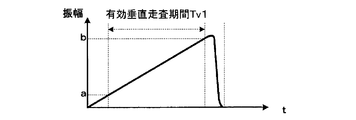
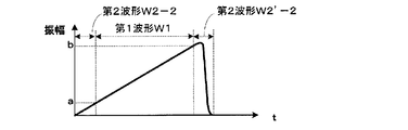
従って、高速走査素子42aの共振周波数frが高いときには無効走査線数n1が多くなり、図6Aに示すように1垂直有効走査期間Tv1が短くなる波形の垂直駆動信号16が必要となる。また、高速走査素子42aの共振周波数frが低いときには無効走査線数n1が少なくなり、図6Bに示すように1垂直有効走査期間Tv1が長くなる波形の垂直駆動信号16が必要となる。なお、表示画像の画像サイズを略一定にするため、高速走査素子42aの傾斜範囲が略一定(図6A,図6Bでは振幅a~bの範囲)になるようにしている。
なお、上述においては、共振周波数frの±1%程度の変動を一つの単位(水平走査10本単位)で無効走査線数n1を変更するようにしたが、これに限らず、例えば、共振周波数frの0.1%程度の変動を一つの単位(水平走査1本単位)で無効走査線数n1を変更し、無効走査線数n1を1本単位で増減させるようにする。これにより、高速走査素子の共振周波数の変動による低速走査素子の揺動周期(低速走査周期)の変動を、高速走査素子42aによる1走査の周期の時間以内、すなわち高速走査素子42aの揺動周期(図2に示す1/frの期間)の1/2の時間(1/fh)以内の変動とすることができ、低速走査素子の揺動周期の変動を最も抑えることができる。
特に、高速走査素子42aの揺動周期(1/fr)の1/2の時間(1/fh)又はその整数倍(n/fh:nは2以上の整数)の単位で総走査線数Nを変動とすることで、低速走査素子44aの垂直走査周波数を高速走査素子42aによる水平走査線数で規定することができる。
本実施形態における画像表示装置1では、このように高速走査素子42aの共振周波数frに応じて垂直駆動信号16の波形を変更するようにすることで垂直駆動信号16の周期を略一定にしており、複数の垂直駆動信号16の波形データを第2及び第3のROM102,103に記憶するようにしている。以下、この点につき具体的に説明する。
(垂直駆動信号16のデータの記憶)
制御部13は駆動信号生成部として、垂直駆動信号16を生成するための鋸歯形状波形のデータを第1波形のデータと第2波形のデータに分けて第2及び第3のROM102,103に記憶する点について説明する。
制御部13は駆動信号生成部として、垂直駆動信号16を生成するための鋸歯形状波形のデータを第1波形のデータと第2波形のデータに分けて第2及び第3のROM102,103に記憶する点について説明する。
垂直駆動信号16のデータは、1周期(1垂直走査期間Tv)分の垂直駆動信号16の鋸歯形状波形を第1波形W1と第2波形W2,W2'とに分割して記憶手段110(第2及び第3のROM102,103)に記憶させているようにしている。
図7に示すように、第1波形W1は、1周期分の垂直駆動信号16の鋸歯形状波形のうち光を走査するための波形であり、垂直有効走査期間Tv1のときの垂直駆動信号16の波形である。また、第2波形W2,W2'は、1周期分の垂直駆動信号16の鋸歯形状波形のうち第1波形W1を除く波形である。第1垂直無効走査期間Tv2-1のときの垂直駆動信号16の波形が第2波形W2であり、第2垂直無効走査期間Tv2-2のときの垂直駆動信号16の波形が第2波形W2'である。第2のROM102には第1波形W1のデータが記憶され、第3のROM103には第2波形W2,W2'のデータが記憶される。
CPU100は、第2及び第3のROM102,103から第1波形W1のデータと第2波形W2,W2'のデータを読み出し、これらのデータを用いて駆動信号データを生成し、RAM104に記憶する。そして、CPU100は、RAM104に記憶した駆動信号データをD/A変換器108(図1参照)でアナログ化することによって1周期分の垂直駆動信号16を生成し、この処理を繰り返すことにより図8に示すように連続する鋸歯形状波形の垂直駆動信号16を生成する。
(第1波形W1について)
記憶手段110における第2のROM102に記憶する第1波形W1は1種類である。表示画像のサイズを略一定にするためには、高速走査素子42aの共振周波数frに応じて垂直駆動信号16のうち第1波形W1部分の傾斜を変更する必要がある。例えば、高速走査素子42aの共振周波数frが31500Hzのときの第1波形W1(図9B参照)は、設計値である30000Hzのとき(図9A参照)の第1波形W1よりも傾斜を急峻にし、高速走査素子42aの共振周波数frが28800Hzのときの第1波形W1(図9C参照)は、設計値である30000Hzのときの第1波形W1(図9A参照)よりも傾斜をなだらかにする必要がある。
記憶手段110における第2のROM102に記憶する第1波形W1は1種類である。表示画像のサイズを略一定にするためには、高速走査素子42aの共振周波数frに応じて垂直駆動信号16のうち第1波形W1部分の傾斜を変更する必要がある。例えば、高速走査素子42aの共振周波数frが31500Hzのときの第1波形W1(図9B参照)は、設計値である30000Hzのとき(図9A参照)の第1波形W1よりも傾斜を急峻にし、高速走査素子42aの共振周波数frが28800Hzのときの第1波形W1(図9C参照)は、設計値である30000Hzのときの第1波形W1(図9A参照)よりも傾斜をなだらかにする必要がある。
そこで、制御部13のCPU100は、この第1波形W1のデータを高速走査素子42aの水平走査周波数fh(=共振周波数fr×2)に応じた周期(=1/fh)の読み出しタイミングで第2のROM102から順次読み出すことにより、高速走査素子42aの共振周波数frに応じて垂直駆動信号16のうち第1波形W1部分の傾斜を変更するようにしている。
例えば、800個のデータで一つの第1波形W1のデータが構成されているとすると、高速走査素子42aの共振周波数frが設計値である30000Hzでは、1/60000秒(=1/fh)毎に第2のROM102からデータが順次読み出され、8/600秒で第1波形W1の全てのデータが読み出される。また、高速走査素子42aの共振周波数frが31500Hzであるときには、1/63000秒(=1/fh)毎に第2のROM102からデータが順次読み出され、8/630秒で第1波形W1の全てのデータが読み出される。従って、垂直駆動信号16のうち第1波形W1部分の傾斜が高速走査素子42aの共振周波数frが30000Hzのときに比べて急峻になる。また、高速走査素子42aの共振周波数frが28800Hzであるときには、1/57600秒(=1/fh)毎に第2のROM102からデータが順次読み出され、8/576秒で第1波形W1の全てのデータが読み出される。従って、垂直駆動信号16のうち第1波形W1部分の傾斜が高速走査素子42aの共振周波数frが30000Hzのときに比べてなだらかになる。
なお、記憶手段110に記憶した第1波形W1のデータの読み出しタイミングは、高速走査素子42aの揺動周期の1/2(=1/fh)に限らず、高速走査素子42aの揺動周期の1/2の整数倍であって、垂直駆動信号16として必要な周波数帯域を抑圧しない周期であればよい。
(第2波形W2,W2'について)
上述したように、高速走査素子42aの共振周波数frに応じて垂直駆動信号16の第1波形W1部分の期間が変わる一方、垂直駆動信号16の周期は1/60秒±0.5%に抑えられることから、高速走査素子42aの共振周波数frに応じて駆動信号の第2波形W2,W2' 部分の期間を変更する必要がある。
上述したように、高速走査素子42aの共振周波数frに応じて垂直駆動信号16の第1波形W1部分の期間が変わる一方、垂直駆動信号16の周期は1/60秒±0.5%に抑えられることから、高速走査素子42aの共振周波数frに応じて駆動信号の第2波形W2,W2' 部分の期間を変更する必要がある。
高速走査素子42aの共振周波数frに応じて第2波形W2,W2'の読み出しタイミングを変えることにより、垂直駆動信号16の第2波形W2,W2'部分の期間を変えて、垂直駆動信号16の周期を1/60秒±0.5%に変えることも考えられる。しかし、上述したように、低速走査素子44aには固有の共振周波数があり、垂直駆動信号16はその低速走査素子44aの共振周波数成分を抑圧しなければならない。単純に第2波形W2,W2'の読み出しタイミングを変えると、垂直駆動信号16の周波数成分が変わってしまい、低速走査素子44aの共振周波数成分が抑圧できない場合がある。
そこで、高速走査素子42aの共振周波数frに応じて複数種類の第2波形W2-1,W2'-1~W2-n,W2'-n(nは2以上の整数。ここではn=11)を第3のROM103には記憶しており、揺動状態検出部42dで検出した高速走査素子42aの共振周波数frに応じて異なる波形を選択することができるようにしている。
記憶手段110における第3のROM103には、図10に示す第2波形テーブルが記憶されている。この第2波形テーブルは、300Hz単位で高速走査素子42aの共振周波数frと第2波形W2-1,W2'-1~W2-11,W2'-11のデータ名とを対応付けたテーブルである。
CPU100は、揺動状態検出部42dから通知される高速走査素子42aの共振周波数frに対応する第2波形W2,W2'のデータ名を第2波形テーブルにより判定し、この判定した第2波形W2,W2'のデータ名に応じた第2波形W2,W2'のデータを第3のROM103から読み出すことになる。
第3のROM103からの読み出しは、第1波形W1を読み出すタイミングと連続したタイミングとしている。このタイミングは、高速走査素子の揺動周期の1/2(=1/fh)又はその整数倍であって、垂直駆動信号16として必要な周波数帯域を抑圧しない周期であればよい。
このようにすることで、低速走査素子44a固有の共振周波数の信号成分を抑圧した垂直駆動信号16を精度よく再現することが可能となる。なお、高速走査素子42aの共振周波数frは、急激に変化するものではなく緩やかに変化することが多いことから、本実施形態では、第1波形W1と第2波形W2,W2'とを第2及び第3のROM102,103から読み出して駆動信号データとしてRAM104に記憶しておくようにしているがこれに限られない。例えば、第1波形W1と第2波形W2,W2'とをRAM104に記憶せずに、第2及び第3のROM102,103から直接第1波形W1と第2波形W2,W2'とを読み出すようにし、D/A変換器108でアナログ信号に変換するようにしてもよい。
なお、第2波形W2,W2'は2つの波形として分けて説明したが、これらの第2波形W2,W2'は連続する(図8参照)ものであり、一つの波形W2"(W2+W2')として第3のROM103に記憶するようにしてもよい。また、第1波形W1と第2波形W2,W2'が1つの波形として第3のROM103に記憶し、読み出す時にアドレス制御などで別波形として読み出される様にしても良いし、もちろん、第1波形が複数記憶されていてもよい。
(画像光の輝度の調整)
上述のように高速走査素子42aの共振周波数frに応じて、無効走査線数n1を変更すると、総走査線数Nに対する有効走査線数n2の割合も変わることになる。低速走査素子44aによる1垂直走査期間Tvは、その変動を所定範囲内に抑えることにより略一定にしていることから、高速走査素子42aの共振周波数frが変動すると、光源部20から画像光を出射する時間が変動し、表示画像の輝度も変動することなる。
上述のように高速走査素子42aの共振周波数frに応じて、無効走査線数n1を変更すると、総走査線数Nに対する有効走査線数n2の割合も変わることになる。低速走査素子44aによる1垂直走査期間Tvは、その変動を所定範囲内に抑えることにより略一定にしていることから、高速走査素子42aの共振周波数frが変動すると、光源部20から画像光を出射する時間が変動し、表示画像の輝度も変動することなる。
そこで、制御部13には高速走査素子の共振周波数と輝度補正割合Kjとを関連付けた輝度テーブルを第3のROM103に記憶している。
この輝度テーブルは、図11に示すように、300Hz間隔で高速走査素子42aの共振周波数と輝度補正割合Kjとを対応付けている。従って、CPU100はこのLUTを参照することにより、高速走査素子の共振周波数frに応じて前記輝度補正割合Kjを変化させて、画像信号供給回路11へ出力する画像信号の輝度情報を変更する。例えば、高速走査素子42aの共振周波数frが28500Hzのときには、CPU100は、画像信号の各輝度信号の強度を0.952倍にして画像信号供給回路11へ出力する。なお、高速走査素子42aの揺動範囲が共振周波数に応じて変化する場合には、その変化分の調整も必要となる。
このように画像信号に応じた光の輝度を高速走査素子42aの共振周波数に応じて変化させて、共振周波数に応じて表示する画像の輝度が変化するのを抑制するので、表示する画像の品質を維持することができる。
(制御部13による光走査部40の制御)
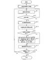
以上のように構成された画像表示装置1の制御部13による光走査部40の制御を図12の動作フロー図を参照して説明する。
以上のように構成された画像表示装置1の制御部13による光走査部40の制御を図12の動作フロー図を参照して説明する。
図12に示すように、制御部13の制御動作が開始されると、まず、CPU100は、所定の水平駆動信号15(例えば、30000Hzの水平駆動信号15)を高速走査素子42aに入力して、高速走査素子42aは反射ミラー42bの揺動を開始させる(ステップS10)。
次に、CPU100は、高速走査素子42aの反射ミラー42bの揺動周波数、揺動の大きさ、位相差などの情報を揺動状態検出部42dから取得し、水平駆動信号15の周波数や振幅を変更する(ステップS11)。
その後、CPU100は、高速走査素子42aが共振状態になったか否かを判定する(ステップS12)。このとき、CPU100は、高速走査素子42aの反射ミラー42bの揺動の大きさや水平駆動信号15と揺動状態との位相差が所定範囲内になると、高速走査素子42aが共振状態になったと判定し、高速走査素子42aの反射ミラー42bの揺動の大きさや位相差が所定範囲外であれば、高速走査素子42aが共振状態になっていないと判定する。
高速走査素子42aが共振状態になっていないと判定すると(ステップS12:No)、CPU100は、高速走査素子42aが共振状態になるのを待つため、再度ステップS11の処理に戻る。なお、所定時間を経ても共振状態にならない場合は、高速走査素子42aの駆動を中止する。
一方、高速走査素子42aが共振状態になっていると判定すると(ステップS12:Yes)、CPU100は、高速走査素子42aの共振周波数を検出する(ステップS12)。すなわち、共振状態になっている高速走査素子42aに入力している水平駆動信号15の周波数を高速走査素子42aの共振周波数とする。そして、CPU100は、高速走査素子42aの共振周波数の情報をRAM104に記憶する(ステップS14)。
次に、CPU100は、今回ステップS14で記憶した共振周波数の値(記憶値)と前回ステップS14で記憶した共振周波数の値(記憶値)が同じ値であるか否かを判定する(ステップS15)。なお、RAM104に記憶される共振周波数の値(記憶値)の初期値は、30000Hzである。従って、最初にこのステップS15の処理を行うときには、この初期値と今回の記憶値が同じ値であるか否かが判定されることになる。
前回の記憶値と今回の記憶値が同じ値ではないと判定すると(ステップS15:No)、CPU100は、第1波形W1を第2のROM102から読み出し、今回の記憶値(高速走査素子42aの共振周波数)に応じた第2波形W2,W2'を第3のROM103の中から選択して読み出する。そして、読み出した第2波形W2,第1波形W1,第2波形W2'を繋げて駆動信号データを生成してRAM104に記憶する(ステップS16)。一方、前回の記憶値と今回の記憶値が同じ値であると判定すると(ステップS15:Yes)、CPU100は、ステップS16の処理を行わない。
そして、CPU100は、垂直駆動信号16を生成する(ステップS17)。すなわち、CPU100は、RAM104に記憶した駆動信号データを、高速走査素子42aの共振周波数に基づいて決められる周期の読み出しクロック信号で順次読み出し、D/A変換器108に入力して垂直駆動信号16を生成して出力する。なお、RAM104に駆動信号データを記憶せずに、第2及び第3のROM102,103から第1波形W1及び第2波形W2,W2'を直接読み出すこともできる。この場合、CPU100は、ステップS16で今回の記憶値(高速走査素子42aの共振周波数)に応じた第2波形W2,W2'を選択する。そして、CPU100は、第3のROM103に記憶された第2波形W2のデータのうちステップS16で選択した第2波形W2のデータ、第2のROM102に記憶した第1波形W1のデータ、第3のROM103に記憶された第2波形W2'のデータのうちステップS16で選択した第2波形W2'のデータの順に、各データを高速走査素子42aの共振周波数に基づいて決められる周期の読み出しクロック信号で読み出す。CPU100は、読み出したクロック信号を、D/A変換器108に入力してD/A変換器108から垂直駆動信号16を出力させる。
以上の処理を利用者による駆動終了指示或は一時停止指示があるまで継続する(ステップS1)。
このように画像表示装置1においては、CPU100は、高速走査素子42aの共振周波数frの情報を揺動状態検出部42dから取得し、この共振周波数に基づいて決められる周期の読み出しクロック信号により記憶手段110に記憶した第1波形W1のデータを順次読み出す。そして、CPU100は、このように読み出したデータをD/A変換器108に入力することにより第1波形W1部分の垂直駆動信号16を生成する。また、CPU100は、高速走査素子42aの共振周波数に応じて記憶手段110に記憶した複数の第2波形W2-1,W2'-1~W2-11,W2'11のデータの中から、鋸歯形状波形の周期の変動を所定時間以内に維持する第2波形W2,W2'のデータを、高速走査素子42aの共振周波数に応じた周期の読み出しタイミングで記憶手段110から順次読み出してD/A変換器に入力することで第2波形部分の垂直駆動信号16を生成する。
従って、高速走査素子の共振周波数などの変動やばらつきによる、垂直走査周波数の変動を抑制し、略一定周波数化でき、かつ、低速走査素子44aの揺動状態を容易に安定させることができる。しかも、第2波形W2,W2'は低速走査素子44a固有の共振周波数の成分を抑圧した波形としたため、低速走査素子44aの反射ミラー44bの共振振動が誘起されることを抑制することができる。
以上、本発明の実施の形態のいくつかを図面に基づいて詳細に説明したが、これらは例示であり、当業者の知識に基づいて種々の変形、改良を施した他の形態で本発明を実施することが可能である。
例えば、上述の実施形態においては、反射ミラー44bが弾性のある梁部材44dを介して固定部材に揺動可能に支持された低速走査素子44aを例に挙げて説明した。しかし、この構成のものに限らず固有の共振周波数を有する低速走査素子であればいずれにも適用することができる。なお、上述した実施例は、低速走査素子の固有共振の課題も解決する例を挙げてきたが、これは最も効果的な一例として挙げた。しかし、前記記憶手段が記憶する波形が、固有共振を抑制する波形でなくても、本発明の主旨には違わない。すなわち、高速走査素子の周波数の変動によって生じる、低速走査素子の駆動周波数(副走査周波数)の変動を一定範囲内に抑えることができるように構成する場合も本発明の実施形態に当然含まれる。
また、上述の実施形態においては、高速走査素子の共振周波数に応じて複数種類の第2波形のデータを記憶手段に記憶し、高速走査素子の共振周波数に応じた種類の第2波形のデータを記憶手段から読み出して第2波形部分の駆動信号を生成する例を挙げて説明した。しかし、これに限らず、高速走査素子の共振周波数に応じて第2波形のデータを当該共振周波数に応じた読み出しタイミングで順次読み出して高速走査素子の共振周波数に応じた第2波形部分の駆動信号を生成するものであればよい。例えば、第2波形が記憶手段に1種類しか記憶されていなくてもよい。この場合、高速走査素子の共振周波数が最も高い場合の第2波形のデータ(構成するデータ数が最も多く、言い換えれば最も期間が長い波形のデータ)を用意し、高速走査素子の共振周波数に応じてそのデータの読み出しアドレスとデータ数を変化させる。このようにすることで、記憶手段に記憶する第2波形のデータ量を低減させることができる。なお、この場合、高速走査素子の共振周波数の変化に応じて読み出されたり読み出されなかったりするデータが存在するが、第2波形のデータのうち第1波形と連続する部分のデータは第1波形のデータ値と同一値又は近似した値とするのが好ましい。
また、上述の実施形態においては、垂直駆動信号16のうち垂直有効走査期間Tv1の部分の波形を第1波形とし、垂直無効走査期間Tv2-1,Tv2-2の部分の波形を第2波形としたが、第1波形に垂直有効走査期間Tv1の部分の波形を含んでいればよく、必ずしも垂直有効走査期間Tv1の部分と全く同一である必要ない。
また、上述の実施形態においては、表示画像の解像度を800×600ピクセル、高速走査素子42aの共振周波数の設計値を30kHz、総走査線数Nを1000本、高速走査素子42aの共振周波数のバラツキ(変動)を±5%(30kHz±1500Hz)とし、共振周波数frの約1%(300Hz)の変動を1つの単位としたが、本発明を簡単に説明するためのものであって、これに限られるものではないことは言うまでもない。
また、上述の実施形態においては、鋸歯形状波形信号として図3に示すような波形の信号を例に挙げて説明したが、光を走査するために略直線部分を含む周期性の波形であればよく、例えば、三角波、台形波、正弦波などであってもよい。
1 画像表示装置
10 表示制御部
11 画像信号供給回路
13 制御部
14 画像信号入力I/F
20 光源部
30 光ファイバ
40 光走査部
42 水平走査部
42a 水平走査部の光走査素子(高速走査素子)
44 垂直走査部
44a 光走査素子(低速走査素子)
50 リレー光学
100 CPU
101 第1のROM
102 第2のROM
103 第3のROM
108 D/A変換器
10 表示制御部
11 画像信号供給回路
13 制御部
14 画像信号入力I/F
20 光源部
30 光ファイバ
40 光走査部
42 水平走査部
42a 水平走査部の光走査素子(高速走査素子)
44 垂直走査部
44a 光走査素子(低速走査素子)
50 リレー光学
100 CPU
101 第1のROM
102 第2のROM
103 第3のROM
108 D/A変換器
Claims (6)
- 画像信号に応じた強度の光を2次元走査して画像を表示する画像表示装置において、
前記画像信号に応じた強度の光を出射する光源部と、
共振揺動する反射ミラーにより入射した光を第1方向に相対的に高速に走査する共振型の高速走査素子と、
入力される駆動信号の信号レベルに応じた方向に反射ミラーを傾斜させ、当該反射ミラーにより入射した光を前記第1方向と略直交する第2方向に相対的に低速に走査する低速走査素子と、
前記高速走査素子の共振周波数を検出する検出部と、
前記高速走査素子の共振周波数に応じた鋸歯形状波形の駆動信号を生成する駆動信号生成部と、
前記駆動信号生成部で生成した前記駆動信号を前記低速走査素子に入力する低速走査素子駆動部と、を備え、
前記駆動信号生成部は、
前記駆動信号の鋸歯形状波形のうち光を有効走査するための第1波形のデータを記憶すると共に、前記駆動信号の鋸歯形状波形のうち第1波形を除く波形である第2波形のデータを記憶する記憶手段と、を備え、
前記高速走査素子の共振周波数に応じた読み出しタイミングで前記記憶手段に記憶した第1波形のデータを順次読み出して前記第1波形部分の前記駆動信号を生成し、前記高速走査素子の共振周波数に応じて前記第2波形のデータを前記読み出しタイミングで順次読み出して前記高速走査素子の共振周波数に応じた前記第2波形部分の前記駆動信号を生成することで、前記鋸歯形状波形の周期の変動を所定時間以内に維持することを特徴とする画像表示装置。 - 前記駆動信号生成部は、前記読み出しタイミングで読み出す前記第1波形部分のデータの総数は一定とする一方、前記読み出しタイミングで読み出す前記第2波形部分のデータの総数は前記高速走査素子の共振周波数に応じて変化させることを特徴とする請求項1に記載の画像表示装置。
- 前記高速走査素子の共振周波数に応じて複数種類の前記第2波形のデータが前記記憶手段に記憶されており、
前記駆動信号生成部は、前記高速走査素子の共振周波数に応じた種類の前記第2波形のデータを前記記憶手段から読み出して前記第2波形部分の前記駆動信号を生成することを特徴とする請求項2に記載の画像表示装置。 - 前記読み出しタイミングの周期は、前記高速走査素子の揺動周期の1/2の時間又はその整数倍であって、前記駆動信号の周波数帯域を抑圧しない周期であることを特徴とする請求項1~3のいずれか1項に記載の画像表示装置。
- 前記所定時間は、前記高速走査素子による1走査の周期の時間とすることを特徴とする請求項1~4のいずれか1項に記載の画像表示装置。
- 前記光源部は、前記画像信号に応じた光の輝度を前記高速走査素子の共振周波数に応じて変化させて、共振周波数に応じて表示する画像の輝度が変化するのを抑制することを特徴とする請求項1~5のいずれか1項に記載の画像表示装置。
Priority Applications (1)
| Application Number | Priority Date | Filing Date | Title |
|---|---|---|---|
| US13/230,558 US20120001961A1 (en) | 2009-03-18 | 2011-09-12 | Image display device |
Applications Claiming Priority (2)
| Application Number | Priority Date | Filing Date | Title |
|---|---|---|---|
| JP2009066513A JP5218186B2 (ja) | 2009-03-18 | 2009-03-18 | 画像表示装置 |
| JP2009-066513 | 2009-03-18 |
Related Child Applications (1)
| Application Number | Title | Priority Date | Filing Date |
|---|---|---|---|
| US13/230,558 Continuation-In-Part US20120001961A1 (en) | 2009-03-18 | 2011-09-12 | Image display device |
Publications (1)
| Publication Number | Publication Date |
|---|---|
| WO2010107071A1 true WO2010107071A1 (ja) | 2010-09-23 |
Family
ID=42739730
Family Applications (1)
| Application Number | Title | Priority Date | Filing Date |
|---|---|---|---|
| PCT/JP2010/054584 Ceased WO2010107071A1 (ja) | 2009-03-18 | 2010-03-17 | 画像表示装置 |
Country Status (3)
| Country | Link |
|---|---|
| US (1) | US20120001961A1 (ja) |
| JP (1) | JP5218186B2 (ja) |
| WO (1) | WO2010107071A1 (ja) |
Cited By (4)
| Publication number | Priority date | Publication date | Assignee | Title |
|---|---|---|---|---|
| WO2012072125A1 (en) * | 2010-12-01 | 2012-06-07 | Lemoptix Sa | A method for projecting an image |
| EP2613306A1 (en) * | 2012-01-05 | 2013-07-10 | LG Electronics, Inc. | Projector, apparatus and method for driving optical scanner thereof |
| JP2014130257A (ja) * | 2012-12-28 | 2014-07-10 | Jvc Kenwood Corp | 画像表示装置、画像表示方法及びプログラム |
| CN103200374B (zh) * | 2012-01-05 | 2016-11-30 | Lg电子株式会社 | 投影仪、用于驱动其光学扫描器的装置和方法 |
Families Citing this family (15)
| Publication number | Priority date | Publication date | Assignee | Title |
|---|---|---|---|---|
| JP6011771B2 (ja) * | 2012-03-30 | 2016-10-19 | ソニー株式会社 | レーザ駆動回路、レーザ駆動方法、プロジェクタ装置、及び、レーザ光を用いる装置 |
| JP6111606B2 (ja) * | 2012-11-08 | 2017-04-12 | ソニー株式会社 | 駆動制御装置および駆動制御方法、並びに映像出力装置 |
| WO2014132447A1 (ja) * | 2013-03-01 | 2014-09-04 | パイオニア株式会社 | 光走査装置 |
| US20160065945A1 (en) * | 2013-04-12 | 2016-03-03 | The Trustees Of Columbia University In The City Of New York | Systems, methods, and media for generating structured light |
| KR20150015530A (ko) | 2013-06-28 | 2015-02-10 | 인텔 코포레이션 | Mems 스캐닝 미러 광 패턴 생성 |
| US9467680B2 (en) | 2013-12-12 | 2016-10-11 | Intel Corporation | Calibration of a three-dimensional acquisition system |
| JP6332736B2 (ja) * | 2014-02-25 | 2018-05-30 | 株式会社リコー | 傾斜動作装置並びにこれを用いた光走査装置及び画像表示装置 |
| JP6544507B2 (ja) * | 2015-02-09 | 2019-07-17 | 日本精機株式会社 | ヘッドアップディスプレイ装置 |
| JP6304068B2 (ja) * | 2015-02-24 | 2018-04-04 | 株式会社Jvcケンウッド | 画像描画装置、ヘッドアップディスプレイ及び画像輝度調整方法 |
| JP6493014B2 (ja) | 2015-06-25 | 2019-04-03 | 株式会社デンソー | 光走査装置 |
| US10659764B2 (en) | 2016-06-20 | 2020-05-19 | Intel Corporation | Depth image provision apparatus and method |
| US10609359B2 (en) | 2016-06-22 | 2020-03-31 | Intel Corporation | Depth image provision apparatus and method |
| JP2017129882A (ja) * | 2017-04-18 | 2017-07-27 | パイオニア株式会社 | 光走査装置 |
| US10861379B2 (en) * | 2019-02-12 | 2020-12-08 | Microsoft Technology Licensing, Llc | Adaptive close loop control for laser beam scanning displays |
| WO2021244533A1 (zh) * | 2020-06-02 | 2021-12-09 | 青岛海信激光显示股份有限公司 | 激光投影设备及激光器驱动控制方法 |
Citations (4)
| Publication number | Priority date | Publication date | Assignee | Title |
|---|---|---|---|---|
| JP2003302590A (ja) * | 2002-04-12 | 2003-10-24 | Canon Inc | 光走査装置およびその駆動方法 |
| JP2006276399A (ja) * | 2005-03-29 | 2006-10-12 | Brother Ind Ltd | 光走査装置、光走査型表示装置及び光走査方法 |
| JP2008077035A (ja) * | 2006-08-23 | 2008-04-03 | Sony Corp | 画像信号の較正方法、これを用いた画像生成装置、画像生成システム及び画像生成方法 |
| JP2009198988A (ja) * | 2008-02-25 | 2009-09-03 | Funai Electric Co Ltd | 画像表示装置 |
Family Cites Families (3)
| Publication number | Priority date | Publication date | Assignee | Title |
|---|---|---|---|---|
| JP2988457B2 (ja) * | 1997-11-10 | 1999-12-13 | 日本電気株式会社 | ディスプレイ装置の駆動装置及び方法 |
| JP5292734B2 (ja) * | 2006-08-08 | 2013-09-18 | セイコーエプソン株式会社 | 走査型画像表示装置 |
| JP5318359B2 (ja) * | 2007-03-29 | 2013-10-16 | コニカミノルタ株式会社 | 画像投影装置 |
-
2009
- 2009-03-18 JP JP2009066513A patent/JP5218186B2/ja not_active Expired - Fee Related
-
2010
- 2010-03-17 WO PCT/JP2010/054584 patent/WO2010107071A1/ja not_active Ceased
-
2011
- 2011-09-12 US US13/230,558 patent/US20120001961A1/en not_active Abandoned
Patent Citations (4)
| Publication number | Priority date | Publication date | Assignee | Title |
|---|---|---|---|---|
| JP2003302590A (ja) * | 2002-04-12 | 2003-10-24 | Canon Inc | 光走査装置およびその駆動方法 |
| JP2006276399A (ja) * | 2005-03-29 | 2006-10-12 | Brother Ind Ltd | 光走査装置、光走査型表示装置及び光走査方法 |
| JP2008077035A (ja) * | 2006-08-23 | 2008-04-03 | Sony Corp | 画像信号の較正方法、これを用いた画像生成装置、画像生成システム及び画像生成方法 |
| JP2009198988A (ja) * | 2008-02-25 | 2009-09-03 | Funai Electric Co Ltd | 画像表示装置 |
Cited By (8)
| Publication number | Priority date | Publication date | Assignee | Title |
|---|---|---|---|---|
| WO2012072125A1 (en) * | 2010-12-01 | 2012-06-07 | Lemoptix Sa | A method for projecting an image |
| CN103238099A (zh) * | 2010-12-01 | 2013-08-07 | 雷模特斯有限公司 | 用于投射图像的方法 |
| US8848269B2 (en) | 2010-12-01 | 2014-09-30 | Lemoptix Sa | Method for projecting an image |
| EP2613306A1 (en) * | 2012-01-05 | 2013-07-10 | LG Electronics, Inc. | Projector, apparatus and method for driving optical scanner thereof |
| CN103200374A (zh) * | 2012-01-05 | 2013-07-10 | Lg电子株式会社 | 投影仪、用于驱动其光学扫描器的装置和方法 |
| US8941781B2 (en) | 2012-01-05 | 2015-01-27 | Lg Electronics Inc. | Projector, apparatus and method for driving optical scanner thereof |
| CN103200374B (zh) * | 2012-01-05 | 2016-11-30 | Lg电子株式会社 | 投影仪、用于驱动其光学扫描器的装置和方法 |
| JP2014130257A (ja) * | 2012-12-28 | 2014-07-10 | Jvc Kenwood Corp | 画像表示装置、画像表示方法及びプログラム |
Also Published As
| Publication number | Publication date |
|---|---|
| US20120001961A1 (en) | 2012-01-05 |
| JP5218186B2 (ja) | 2013-06-26 |
| JP2010217736A (ja) | 2010-09-30 |
Similar Documents
| Publication | Publication Date | Title |
|---|---|---|
| JP5218186B2 (ja) | 画像表示装置 | |
| JP4840175B2 (ja) | 画像表示装置 | |
| JP5674437B2 (ja) | 表示装置 | |
| CN105247601B (zh) | 显示装置 | |
| US20110170156A1 (en) | Optical scanning device, image display device and method of driving optical scanning device | |
| US10089911B2 (en) | Scanning display device | |
| JP2011180277A (ja) | 画像表示装置 | |
| JP5098759B2 (ja) | 画像投影装置 | |
| JP2010237536A (ja) | 画像表示装置 | |
| JP2012155020A (ja) | 走査型画像表示装置 | |
| JP2011075957A (ja) | 画像表示装置 | |
| KR102376402B1 (ko) | 다초점 디스플레이 디바이스 및 방법 | |
| JP2012003051A (ja) | 走査型画像表示装置 | |
| JP2014132295A (ja) | レーザービーム表示装置 | |
| JP5152075B2 (ja) | 駆動信号発生器及びそれを備えた光走査装置並びに画像表示装置 | |
| JP2007286423A (ja) | 光走査装置及び画像表示装置並びに網膜走査型画像表示装置 | |
| JP5565270B2 (ja) | 走査方法、映像投影装置および画像取得装置 | |
| JP5152074B2 (ja) | 駆動信号発生器及びそれを備えた光走査装置並びに画像表示装置 | |
| JP2011164121A (ja) | 画像表示装置 | |
| JP2008089930A (ja) | 画像表示装置及び網膜走査型画像表示装置 | |
| JP2011075958A (ja) | 画像表示装置 | |
| JP2019133068A (ja) | 投影装置およびその制御方法ならびにプログラム | |
| JP5854120B2 (ja) | 表示装置 | |
| JP2005292380A (ja) | コヒーレント光を用いるディスプレイ | |
| JP2018155846A (ja) | 投影装置、制御方法、プログラム及び記憶媒体 |
Legal Events
| Date | Code | Title | Description |
|---|---|---|---|
| 121 | Ep: the epo has been informed by wipo that ep was designated in this application |
Ref document number: 10753562 Country of ref document: EP Kind code of ref document: A1 |
|
| NENP | Non-entry into the national phase |
Ref country code: DE |
|
| 122 | Ep: pct application non-entry in european phase |
Ref document number: 10753562 Country of ref document: EP Kind code of ref document: A1 |