WO2010104064A1 - Memsセンサ - Google Patents
Memsセンサ Download PDFInfo
- Publication number
- WO2010104064A1 WO2010104064A1 PCT/JP2010/053864 JP2010053864W WO2010104064A1 WO 2010104064 A1 WO2010104064 A1 WO 2010104064A1 JP 2010053864 W JP2010053864 W JP 2010053864W WO 2010104064 A1 WO2010104064 A1 WO 2010104064A1
- Authority
- WO
- WIPO (PCT)
- Prior art keywords
- substrate
- layer
- thickness
- mems sensor
- support substrate
- Prior art date
- Legal status (The legal status is an assumption and is not a legal conclusion. Google has not performed a legal analysis and makes no representation as to the accuracy of the status listed.)
- Ceased
Links
Images








Classifications
-
- B—PERFORMING OPERATIONS; TRANSPORTING
- B81—MICROSTRUCTURAL TECHNOLOGY
- B81B—MICROSTRUCTURAL DEVICES OR SYSTEMS, e.g. MICROMECHANICAL DEVICES
- B81B7/00—Microstructural systems ; Auxiliary parts of microstructural devices or systems
- B81B7/0032—Packages or encapsulation
- B81B7/0045—Packages or encapsulation for reducing stress inside of the package structure
- B81B7/0048—Packages or encapsulation for reducing stress inside of the package structure between the MEMS die and the substrate
-
- G—PHYSICS
- G01—MEASURING; TESTING
- G01P—MEASURING LINEAR OR ANGULAR SPEED, ACCELERATION, DECELERATION, OR SHOCK; INDICATING PRESENCE, ABSENCE, OR DIRECTION, OF MOVEMENT
- G01P15/00—Measuring acceleration; Measuring deceleration; Measuring shock, i.e. sudden change of acceleration
- G01P15/02—Measuring acceleration; Measuring deceleration; Measuring shock, i.e. sudden change of acceleration by making use of inertia forces using solid seismic masses
- G01P15/08—Measuring acceleration; Measuring deceleration; Measuring shock, i.e. sudden change of acceleration by making use of inertia forces using solid seismic masses with conversion into electric or magnetic values
- G01P15/0802—Details
-
- G—PHYSICS
- G01—MEASURING; TESTING
- G01P—MEASURING LINEAR OR ANGULAR SPEED, ACCELERATION, DECELERATION, OR SHOCK; INDICATING PRESENCE, ABSENCE, OR DIRECTION, OF MOVEMENT
- G01P15/00—Measuring acceleration; Measuring deceleration; Measuring shock, i.e. sudden change of acceleration
- G01P15/02—Measuring acceleration; Measuring deceleration; Measuring shock, i.e. sudden change of acceleration by making use of inertia forces using solid seismic masses
- G01P15/08—Measuring acceleration; Measuring deceleration; Measuring shock, i.e. sudden change of acceleration by making use of inertia forces using solid seismic masses with conversion into electric or magnetic values
- G01P15/125—Measuring acceleration; Measuring deceleration; Measuring shock, i.e. sudden change of acceleration by making use of inertia forces using solid seismic masses with conversion into electric or magnetic values by capacitive pick-up
-
- G—PHYSICS
- G01—MEASURING; TESTING
- G01P—MEASURING LINEAR OR ANGULAR SPEED, ACCELERATION, DECELERATION, OR SHOCK; INDICATING PRESENCE, ABSENCE, OR DIRECTION, OF MOVEMENT
- G01P15/00—Measuring acceleration; Measuring deceleration; Measuring shock, i.e. sudden change of acceleration
- G01P15/18—Measuring acceleration; Measuring deceleration; Measuring shock, i.e. sudden change of acceleration in two or more dimensions
-
- B—PERFORMING OPERATIONS; TRANSPORTING
- B81—MICROSTRUCTURAL TECHNOLOGY
- B81B—MICROSTRUCTURAL DEVICES OR SYSTEMS, e.g. MICROMECHANICAL DEVICES
- B81B2201/00—Specific applications of microelectromechanical systems
- B81B2201/02—Sensors
- B81B2201/0228—Inertial sensors
- B81B2201/0235—Accelerometers
-
- G—PHYSICS
- G01—MEASURING; TESTING
- G01P—MEASURING LINEAR OR ANGULAR SPEED, ACCELERATION, DECELERATION, OR SHOCK; INDICATING PRESENCE, ABSENCE, OR DIRECTION, OF MOVEMENT
- G01P15/00—Measuring acceleration; Measuring deceleration; Measuring shock, i.e. sudden change of acceleration
- G01P15/02—Measuring acceleration; Measuring deceleration; Measuring shock, i.e. sudden change of acceleration by making use of inertia forces using solid seismic masses
- G01P15/08—Measuring acceleration; Measuring deceleration; Measuring shock, i.e. sudden change of acceleration by making use of inertia forces using solid seismic masses with conversion into electric or magnetic values
- G01P2015/0805—Measuring acceleration; Measuring deceleration; Measuring shock, i.e. sudden change of acceleration by making use of inertia forces using solid seismic masses with conversion into electric or magnetic values being provided with a particular type of spring-mass-system for defining the displacement of a seismic mass due to an external acceleration
- G01P2015/0808—Measuring acceleration; Measuring deceleration; Measuring shock, i.e. sudden change of acceleration by making use of inertia forces using solid seismic masses with conversion into electric or magnetic values being provided with a particular type of spring-mass-system for defining the displacement of a seismic mass due to an external acceleration for defining in-plane movement of the mass, i.e. movement of the mass in the plane of the substrate
- G01P2015/0811—Measuring acceleration; Measuring deceleration; Measuring shock, i.e. sudden change of acceleration by making use of inertia forces using solid seismic masses with conversion into electric or magnetic values being provided with a particular type of spring-mass-system for defining the displacement of a seismic mass due to an external acceleration for defining in-plane movement of the mass, i.e. movement of the mass in the plane of the substrate for one single degree of freedom of movement of the mass
- G01P2015/0814—Measuring acceleration; Measuring deceleration; Measuring shock, i.e. sudden change of acceleration by making use of inertia forces using solid seismic masses with conversion into electric or magnetic values being provided with a particular type of spring-mass-system for defining the displacement of a seismic mass due to an external acceleration for defining in-plane movement of the mass, i.e. movement of the mass in the plane of the substrate for one single degree of freedom of movement of the mass for translational movement of the mass, e.g. shuttle type
-
- H—ELECTRICITY
- H10—SEMICONDUCTOR DEVICES; ELECTRIC SOLID-STATE DEVICES NOT OTHERWISE PROVIDED FOR
- H10D—INORGANIC ELECTRIC SEMICONDUCTOR DEVICES
- H10D48/00—Individual devices not covered by groups H10D1/00 - H10D44/00
- H10D48/50—Devices controlled by mechanical forces, e.g. pressure
Definitions
- the present invention relates to a MEMS sensor formed by bonding an insulating layer between a support substrate and a functional layer having a sensor portion and an anchor portion.
- Patent Document 1 discloses a capacitive dynamic quantity sensor device having a support substrate, a semiconductor layer (functional layer), and a circuit chip.
- This patent document defines the relationship between the gap distance between the movable electrode and the support substrate constituting the semiconductor layer, the gap distance between the movable electrode and the circuit chip, and the thickness of the movable electrode.
- the relationship between the gap distance and the thickness of the movable electrode is defined to prevent the movable electrode from running on the fixed electrode.
- the present invention is intended to solve the above-described conventional problems, and in particular, it is an object of the present invention to provide a MEMS sensor in which stable and highly accurate detection accuracy can be obtained by optimizing the relationship between substrate thicknesses.
- the MEMS sensor according to the present invention is formed of a first substrate, a sensor layer, and a functional layer having an anchor portion integrally formed with the sensor portion, and an insulating material for bonding the anchor portion and the first substrate.
- a first bonding layer, and the sensor unit is spaced apart from the first substrate,
- the thickness of the first substrate may be in the range of 10 times to 30 times the thickness of the functional layer.
- the warp amount of the MEMS sensor can be reduced, and stable and highly accurate detection characteristics can be obtained.
- the semiconductor device further includes a second substrate opposed to the first substrate via the functional layer,
- the sensor unit may be spaced apart from the first substrate and the second substrate, and the anchor unit may be fixed and supported via the second substrate and the second bonding layer.
- the upper and lower portions of the anchor portion are fixed and supported by the bonding layer.
- thermal stress, processing stress, and force based on actual use are applied to the MEMS sensor, as described above, the thickness of the first substrate is 10 times to 30 times the thickness of the functional layer.
- the stress which acts on an anchor part can be reduced effectively. This makes it possible to realize a MEMS sensor having high impact resistance and excellent detection characteristics.
- the first substrate and the second substrate are formed of the same material. Therefore, the amount of deformation in the planar direction of the anchor portion due to the thermal stress can be reduced.
- the first substrate and the second substrate be formed to have the same thickness.
- the first substrate and the second substrate be formed of silicon.
- one of the first substrate and the second substrate may be formed of silicon and the other may be formed of glass, and the first substrate and the second substrate may be formed to have the same thickness. Thereby, the amount of deformation in the planar direction of the anchor portion due to the thermal stress can be reduced.
- an insulating layer is provided on the surface of the second substrate facing the first substrate, the second bonding layer is formed of a metal bonding layer, and the second bonding layer is connected to the second bonding layer.
- the lead layer can be embedded in the insulating layer.
- an insulating layer is provided on the surface opposite to the surface facing the first substrate of the second substrate, and the second bonding layer is formed of a metal bonding layer, and the second bonding is performed.
- a lead layer connected via the layer and the second substrate may be embedded in the insulating layer.
- both the first substrate and the functional layer be formed of silicon.
- the MEMS sensor of the present invention by optimizing the relationship of the substrate thickness, it is possible to obtain stable and highly accurate detection accuracy as compared with the prior art.
- FIG. 1 (a) is a plan view of the MEMS sensor (acceleration sensor) in the first embodiment
- FIG. 1 (b) is a longitudinal sectional view of the MEMS sensor cut from line AA of FIG. 1 (a) and viewed from the arrow direction.
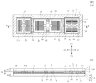
- Fig.2 (a) is a top view of the MEMS sensor (acceleration sensor) in 2nd Embodiment
- FIG.2 (b) is a longitudinal cross-section of the MEMS sensor cut
- FIG. 4 is a partially enlarged vertical cross-sectional view of a MEMS sensor showing a cross-sectional shape different from FIG. 3.
- the graph which shows the relationship of the thickness ratio with respect to the functional layer of a support substrate, and curvature amount.
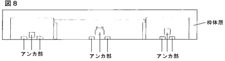
- FIG. 8 is a plan view of the functional layer of FIG. 7; The enlarged schematic diagram of the lamination substrate for explaining an experiment position.
- the graph which shows the relation between the position of an anchor part, and the maximum stress which acts on an anchor part.
- the schematic diagram of the laminated substrate used by experiment The schematic diagram which expanded and showed a part of FIG. 12 for demonstrating the height position of an anchor part, and the position to a X direction.
- FIG. 1 (a) is a plan view of the MEMS sensor (acceleration sensor) in the first embodiment
- FIG. 1 (b) is a longitudinal sectional view of the MEMS sensor cut from line AA of FIG. 1 (a) and viewed from the arrow direction. It is a face view.
- the MEMS sensor shown in FIG. 1 is formed in a laminated structure having a support substrate (first substrate) 1, a functional layer 2, and a first bonding layer 3.
- the MEMS sensor is formed, for example, by micromachining an SOI substrate.
- the support substrate 1 and the functional layer 2 are preferably formed of silicon, and the first bonding layer 3 is preferably formed of silicon oxide.
- the thickness of the first bonding layer 3 is preferably in the range of 0.5 to 2.0 ⁇ m.
- the width dimension and the length dimension (longitudinal dimension in the XY plane) of the support substrate 1 and the functional layer 2 are about 0.5 to 2.5 mm.
- the sensor portion 4 anchor portions 5 and 10, support beams 6 and the like are formed by fine processing. Furthermore, the sensor unit 4 is configured to have a weight 7, a movable electrode 8 and a fixed electrode 9. As shown in FIG. 1A, the comb-like movable electrode 8 and the comb-like fixed electrode 9 are alternately arranged. The movable electrode 8, the weight 7, the support beam 6 and the anchor 5 are integrally formed. On the other hand, the fixed electrode 9 is formed integrally with the anchor portion 10 in a state of being separated from the movable electrode 8 and the weight portion 7.
- the anchor portions 5 and 10 are fixedly supported on the support substrate 1 via the first bonding layer 3.
- a space is formed between the sensor unit 4 and the support substrate 1.
- the weight portion 7 is displaced by receiving a force (inertial force) accompanying the acceleration, and based on a change in capacitance between the movable electrode 8 and the fixed electrode 9, the change in acceleration or the magnitude of the acceleration Can be detected.
- the thickness of the support substrate 1 is H1
- the thickness of the functional layer 2 is H2.
- the thickness H2 of the functional layer 2 is constant, but in the embodiment in which the thickness is different depending on the location of the functional layer 2, the thickness H2 of the functional layer 2 is the thickness of the anchor portions 5 and 10. It is defined. The same applies to the embodiment shown in FIG.
- the thickness H1 of the support substrate 1 is formed in a range of 10 times to 30 times the thickness H2 of the functional layer 2.
- the thickness H1 of the support substrate 1 is preferably in the range of 200 to 900 ⁇ m, and the thickness H2 of the functional layer 2 is preferably in the range of 20 to 30 ⁇ m.
- the thickness H2 of the functional layer 2 is about 20 ⁇ m, and the thickness H1 of the support substrate 1 is adjusted in the range of 200 ⁇ m to 600 ⁇ m.
- the warpage amount of the MEMS sensor can be effectively reduced by defining the thickness ratio between the support substrate 1 and the functional layer 2 as described above.
- the support substrate 1 and the functional layer 2 are preferably formed of silicon
- the present invention is not limited to silicon as long as the support substrate 1 and the functional layer 2 are the same material.
- the term "same material” as used herein means that mechanical properties (here, Poisson's ratio, Young's modulus, and thermal expansion coefficient) are substantially equal. If each mechanical property is a difference within 10% between the support substrate 1 and the functional layer 2 (a ratio obtained by dividing the difference of the mechanical property by the mechanical property of the larger value), "the same material” Define as Therefore, different materials can be used for the support substrate 1 and the functional layer 2 as long as the mechanical properties are substantially the same.
- FIG.2 (a) is a top view of the MEMS sensor (acceleration sensor) in 2nd Embodiment
- FIG.2 (b) is a longitudinal cross section of the MEMS sensor cut
- the plan view of FIG. 2A is shown through the support substrate 1.
- the MEMS sensor illustrated in FIG. 2 has, for example, a rectangular shape in which the X direction is a long side and the Y direction is a short side.
- the MEMS sensor shown in FIG. 2B includes a sensor unit 20 including the support substrate 1, the first bonding layer 3 and the functional layer 2, and the sensor unit facing the sensor unit 20 and formed in the sensor unit 20.
- a cap member 12 for sealing is stacked.
- the width dimension and the length dimension (longitudinal dimension in the XY plane) of the sensor unit 20 and the cap member 12 are about 0.5 to 2.5 mm.
- the cap member 12 is configured of a cap substrate (second substrate) 13, an insulating layer 14 formed on the surface thereof, and a second bonding layer 15.
- the insulating layer 14 is preferably formed of silicon oxide.
- the insulating layer 14 is preferably formed to a thickness of about 0.5 to 2.0 ⁇ m.
- the second bonding layer 15 is preferably formed to a thickness of about 0.5 to 1.5 ⁇ m. The material of the second bonding layer 15 will be described later.
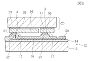
- FIG. 3 is a partially enlarged longitudinal sectional view showing a part of FIG. 2 (b) in an enlarged manner.
- the cap member 12 is formed so as to protrude from the sensor unit 20.
- a conductor pattern is embedded in the insulating layer 14 to form a lead layer 35.
- the lead layer 35 is separately conducted to the movable electrode and the fixed electrode of the detection portion formed on the functional layer 2 and is conducted to the external connection pads 50 provided outside the MEMS sensor.
- a frame layer 11 is formed in the peripheral region of the functional layer 2, and the inside of the frame layer 11 is a forming area of the sensor portion.
- the frame layer 11 is indicated by oblique lines.
- a first hole 26, a second hole 27, and a third hole 28 for defining the outer shape of the sensor portion are formed inside the frame layer 11.
- the respective holes 26, 27, 28 pass through the frame layer 11 in the thickness direction.
- a frame-shaped first bonding layer 3 is formed in the facing portion of the support substrate 1 and the frame layer 11.
- the second bonding layer 15 seals the periphery of the sensor portion between the frame layer 11 and the insulating layer 14 formed on the facing surface of the cap member 12. doing.
- the insides of the respective holes 26, 27, 28 are sensor portions 16, 17, 18.
- the MEMS sensor shown in FIG. 2 can detect the acceleration in the Z direction of the direction orthogonal to the substrate surface of the support substrate 1 by the operation of the first movable body 41 provided in the first sensor unit 16. Further, by the operation of the second movable body 21 provided in the second sensor unit 17, acceleration in the Y direction parallel to the substrate surface of the support substrate 1 can be detected, and the third sensor unit 18 is provided with a third acceleration. The acceleration of the X direction orthogonal to the Z direction and the Y direction can be detected by the operation of the movable body 21A.
- the second movable body 21 is provided inside the second hole 27.
- the second movable body 21 is supported movably mainly in the Y direction by the anchor portions 23 and 25.
- the anchor portions 23 and 25 are joined via the insulating and insulating layer 14 and the second bonding layer 15.
- the anchor portions 23 and 25 are fixed by being sandwiched from above and below by the first bonding layer 3 and the second bonding layer 15, but the second movable body 21 is And is not bonded to the support substrate 1 nor to the insulating layer 14.
- the second movable body 21 shown in FIG. 2A is provided with a plurality of movable electrodes in a comb shape. At least one of the anchor portions 23 and 25 is electrically connected to the lead layer 35 provided inside the insulating layer 14 via the second bonding layer 15, and the lead layer 35 is a cap member protruding to the outside of the sensor unit 20. It is conductively connected to an external connection pad 50 provided on the exposed surface of 12 (see FIG. 3).
- the fixing portions 31 and 32 are provided.
- the anchor portion 33 is integrally formed on the fixing portion 31.
- the anchor portion 34 is integrally formed with the fixing portion 32.
- the anchor portion 33 is bonded to the support substrate 1 via the first bonding layer 3. Further, the insulating layer 14 formed on the surface of the cap substrate 13 and the anchor portion 33 are bonded by the second bonding layer 15.
- a plurality of fixed electrodes are integrally formed in a comb shape. Each fixed electrode is inserted between a plurality of movable electrodes integrally formed on the second movable body 21.
- the fixing portion 32 also has the same configuration as the fixing portion 31.
- the anchor portions 33 and 34 are connected to the second bonding layer 15, and the second bonding layer 15 is connected to a lead layer provided inside the insulating layer 14.
- the lead layer is conductively connected to an external connection pad 50 provided on the exposed surface of the cap member 12 protruding to the outside of the sensor unit 20.
- the second sensor unit 17 of the MEMS sensor shown in FIG. 2 responds to the acceleration in the Y1 direction or the Y2 direction.
- the reaction causes the second movable body 21 to move in the Y2 direction.
- the capacitance changes as the facing distance between the movable electrode and the fixed electrode changes. Then, it is possible to detect the change in acceleration acting in the Y1 direction and the magnitude of the acceleration by the change in capacitance.
- the structure of the third sensor unit 18 shown in FIG. 2A is exactly the same as that obtained by rotating the structure of the second sensor unit 17 by 90 degrees.
- the third sensor unit 18 operates in reaction to the acceleration in the X1-X2 direction.
- acceleration in the X1 or X2 direction acts on the MEMS sensor
- the inertial force moves the third movable body 21A in the direction opposite to the acting direction of the acceleration, and the amount of movement at that time is the movable electrode and the fixed electrode It is detected as a change in capacitance at the opposing detection unit.
- a first movable body 41 is provided.
- the first movable body 41 is supported by the anchor portions 42 and 42 so as to be movable in the Z direction.
- Each anchor portion 42, 42 is bonded to the support substrate 1 by the first bonding layer 3.
- the anchor portions 42 and 42 are bonded to the insulating layer 14 formed on the surface of the cap substrate 13 by the second bonding layer 15.
- the first movable body 41 is separated from the support substrate 1 and the insulating layer 14 so that movement in the Z direction is possible.
- a plurality of movable electrodes are integrally formed in a comb shape. Then, at least one of the anchor portions 42 and 42 is electrically connected to the lead layer in the insulating layer 14 via the second bonding layer 15, and the lead layer is an exposed surface of the cap member 12 protruding outside the sensor unit 20. It electrically connects to the external connection pad 50 provided in.
- fixed portions 51 and 53 are formed separately from the first movable body 41 inside the first movable body 41.
- the anchor portion 52 is integrally formed with the fixing portion 51
- the anchor portion 54 is integrally formed with the fixing portion 53.
- the anchor portion 52 and the anchor portion 54 are respectively bonded to the support substrate 1 by the first bonding layer 3.
- the anchor portion 52 and the anchor portion 54 are respectively bonded to the insulating layer 14 formed on the surface of the cap substrate 13 by the second bonding layer 15.
- portions other than the anchor portions 52 and 54 are separated from the support substrate 1 and the insulating layer 14.
- a plurality of fixed electrodes are integrally formed in a comb shape.
- the fixed electrode is bonded to the lead layer in the insulating layer 14 via the anchor portions 52 and 54 and the second bonding layer 15.
- the lead layer is conductively connected to an external connection pad 50 provided on the exposed surface of the cap member 12 protruding outside the sensor unit 20.
- the first sensor unit 16 can respond to acceleration in the Z direction. For example, when an acceleration in the Z2 direction acts on the MENS sensor, the reaction causes the first movable body 41 to move in the Z1 direction. At this time, the capacitance changes due to the change in the facing area between the movable electrode and the fixed electrode, and the magnitude and change in acceleration can be detected based on the change in capacitance.
- the second bonding layer 15 is formed by eutectic bonding of a first metal layer 56 provided on the sensor unit 20 side and a second metal layer 57 provided on the cap member 12 side. It is formed by diffusion bonding.
- Examples of the combination of materials of the first metal layer 56 and the second metal layer 57 include aluminum-germanium, aluminum-zinc, gold-silicon, gold-indium, gold-germanium, gold-tin and the like. The combination of these metals makes it possible to perform bonding at a relatively low temperature of 450 ° C. or less, which is a temperature below the melting point of each metal.
- the MEMS sensor shown in FIG. 2 constitutes a three-axis acceleration sensor.
- the upper and lower portions of each of the anchor portions 23, 25, 33, 34, 42, 52, 54 are fixedly supported on the side of the support substrate 1 and the cap substrate 13 by the bonding layers 3 and 15.
- the thickness H1 of the support substrate 1 is formed in a range of 10 times to 30 times the thickness H2 of the functional layer 2.
- a thermal stress, a processing stress, and a force based on the actual use are applied to the MEMS sensor, but the thickness H1 of the support substrate (first substrate) 1 is set to the thickness H2 of the functional layer 2 as described above.
- the stress acting on each anchor portion 23, 25, 33, 34, 42, 52, 54 can be effectively reduced. This makes it possible to realize a MEMS sensor having high impact resistance and excellent detection characteristics.
- a cap substrate 13 is provided in addition to the support substrate 1 and the functional layer 2.
- the thickness of the cap substrate 13 is H3.
- the support substrate 1 and the cap substrate 13 be formed of the same material.
- “the same material” indicates that mechanical properties (here, Poisson's ratio, Young's modulus, and thermal expansion coefficient) are substantially equal.
- the support substrate 1 and the cap substrate 13 be formed of silicon.
- the thickness H3 of the cap substrate 13 can be defined within the range of the thickness H1 of the support substrate 1 described above. It is preferable to make H1 and the thickness H3 of the cap substrate 13 the same. The manufacturing error is in the range of the same thickness.
- one of the support substrate 1 and the cap substrate 13 may be made of silicon and the other may be made of glass, and the thickness H1 of the support substrate 1 and the thickness H3 of the cap substrate 13 may be the same.
- the support substrate 1 is formed of silicon and the cap substrate 13 is formed of glass.
- each anchor portion 23, 25, 33, 34, 42, 52, 54 resulting from the thermal stress can be obtained by matching the material and thickness with the support substrate 1.
- the amount of deformation in the (XY plane direction) can be reduced. Therefore, it is possible to obtain more stable, highly accurate detection characteristics more effectively.
- the cap substrate 13 may be an IC substrate. Also, it is possible to make the cross-sectional structure shown in FIG. 4 differently from FIG.
- a through wiring layer 30 penetrating the cap substrate 13 is provided.
- the through wiring layer 30 can be formed separately from the cap substrate 13.
- An insulating layer 29 insulates between the through wiring layer 30 and the cap substrate 13.
- the through wiring layer 30 and the anchor portion are joined via the second bonding layer 15 composed of the first metal layer 56 and the second metal layer 57 described in FIG. There is.
- the insulating layer 29 covers the surface opposite to the surface facing the functional layer 2 of the cap substrate 13 and the opposite surface 13 a side, and as shown in FIG. 4, the lead layer 37 in contact with the through wiring layer 30 is inside the insulating layer 29. It is formed. A part of the lead layer 37 is exposed from the surface of the insulating layer 29 to constitute an external connection pad.
- the present embodiment is not limited to the acceleration sensor.
- the MEMS sensor 1 of the capacitance type is used, but the invention is not limited to the capacitance type.
- the thickness ratio of the support substrate (first substrate) to the functional layer-Experiment of the amount of warpage was conducted using a laminated substrate in which a functional layer made of silicon is stacked on a supporting substrate made of silicon in a circular shape having a diameter of 152 mm.
- the Poisson's ratio of the support substrate was 0.17.
- Young's modulus was 150 GPa.
- the thickness H2 of the functional layer was unified at 20 ⁇ m.
- a first bonding layer made of an insulating material is actually present between the support substrate and the functional layer, the experiment was performed with a film stress of 10 MPa due to the presence of the first bonding layer.
- the film stress of 10 MPa corresponds to the case where the first bonding layer is made of silicon oxide of about 1 to 2 ⁇ m.
- ⁇ is the film stress
- ⁇ is the Poisson's ratio of the support substrate
- H 2 is the thickness of the functional layer
- L is the length (diameter) of the support substrate
- E is the Young's modulus of the support substrate
- H 1 is the thickness of the support substrate is there.
- the thickness H1 of the support substrate is set in a range of 10 times to 30 times the thickness H2 of the functional layer, the amount of warpage can be appropriately reduced.
- the larger the thickness ratio of the support substrate to the functional layer the smaller the amount of warpage.
- the height of the MEMS sensor is reduced ( The upper limit is set to 30 times because the size reduction is inhibited.
- FIG. 8 is a plan view of the functional layer shown in FIG.
- the laminated substrate according to this experiment is a half model of the MEMS sensor of FIG.
- the functional layer is composed of an anchor portion and a frame layer fixed and supported on both the support substrate side and the cap substrate side.
- the thickness H3 of the cap substrate was fixed at 200 ⁇ m and the thickness H2 of the functional layer was fixed at 20 ⁇ m. Further, the width dimension of the supporting substrate and the cap substrate is 2.5 mm, and the length dimension orthogonal to the width dimension is 0.76 mm.
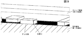
- the “position” shown in FIG. 10 refers to the bonding position of the side surface of the anchor portion shown in FIG. 9 with the supporting substrate (the substrate on which the force is directly applied) as the reference position 0, and points upward from this reference position 0 Point to the side position of the anchor part.
- FIG. 11 is a graph in which the maximum stress of the anchor portion at a position (corresponding to the bonding position with the cap substrate) separated upward by 20 ⁇ m from the reference position 0 is plotted for each thickness H1 of each supporting substrate.
- the ratio of the thickness H1 of the support substrate to the thickness H2 (20 ⁇ m) of the functional layer is 10 to 30 times the anchor portion by making the ratio of 10 to 30 It has been found that the maximum stress acting can be reduced.
- the substrate thickness of the MEMS sensor in which the upper and lower portions of the anchor portion are fixedly supported by the substrate, it is possible to suppress a defect such as breakage from the anchor portion even if a force due to an external factor or the like is applied. It has been found that stable and highly accurate detection characteristics can be obtained.
- a simulation experiment was conducted using a laminated substrate in which a support substrate (first substrate) made of silicon, a functional layer made of silicon, and a cap substrate (second substrate) made of silicon shown in FIG. 12 are stacked.
- the functional layer has a structure of an anchor portion as shown in FIG. 12, and is fixed and supported on both the support substrate side and the cap substrate side.
- a first bonding layer (1 ⁇ m in thickness) made of silicon oxide is interposed between the support substrate and the functional layer, and an insulating oxide layer made of silicon oxide, the first layer of aluminum-germanium is formed between the functional layer and the cap substrate.
- the experiment was conducted on the assumption that the two bonding layers (the combined thickness of the oxide insulating layer and the second bonding layer is 1 ⁇ m) intervened (see FIGS. 2 and 3 for the structure).
- the linear expansion coefficient (22 ° C.) of silicon is 2.60 ⁇ 10 ⁇ 6
- the Young's modulus is 150 GPa
- the Poisson's ratio is 0.17
- the linear expansion coefficient (22 ° C.) of glass is 3.25 ⁇ 10 ⁇ 6
- the Young's modulus was 63 GPa
- the Poisson's ratio was 0.25
- the linear expansion coefficient (22 ° C.) of silicon oxide was 0.56 ⁇ 10 -6
- the Young's modulus was 72 GPa
- the Poisson's ratio was 0.25.
- the thickness H1 of the support substrate was fixed at 200 ⁇ m
- the thickness H2 of the functional layer was fixed at 20 ⁇ m.
- the width dimension of the supporting substrate and the cap substrate is 0.5 mm
- the length dimension orthogonal to the width dimension is 0.5 mm.
- position in the X direction refers to the bonding position of the side surface of the anchor portion with the supporting substrate (in fact, the bonding position with the first bonding layer) as the reference position 0 as shown in FIG. It is shown by the side position to the X direction of the anchor portion at each height position from the reference position 0 toward the upper direction (direction toward the cap substrate).
- FIG. 14 shows the relationship between the position in the X direction of the anchor portion and the height position. As shown in FIG. 14, it was found that when the cap substrate is made of glass, the position of the anchor portion in the X direction gradually increases as the position away from the reference position 0. In addition, it was found that when the cap substrate is made of silicon, the position of the anchor portion in the X direction slightly fluctuates, but this is not so much as when the cap substrate is made of glass.
- FIG. 16 shows the reference position 0, the height position separated by 10 ⁇ m from the reference position 0, and the height position separated by 20 ⁇ m from the reference position 0 with respect to the thickness H3 of each cap substrate when the cap substrate is glass. It is the graph which plotted the position to the X direction in.
- FIG. 17 shows the reference position 0, the height position separated by 10 ⁇ m from the reference position 0, and the height position separated by 20 ⁇ m from the reference position 0 with respect to the thickness H3 of each cap substrate when the cap substrate is silicon It is the graph which plotted the position to the X direction in.
- the cap substrate is formed of the same silicon as the support substrate, the amount of deformation of the anchor portion in the X direction becomes very small.
- the cap substrate is made of glass, the amount of deformation of the anchor portion in the X direction is larger than when the cap substrate is made of silicon, but when the cap substrate is 200 ⁇ m the same as the support substrate, the anchor portion is most It was found that the amount of deformation of can be reduced.
- the film thickness difference between the cap substrate and the support substrate is preferably within 100 ⁇ m, and the thickness of the cap substrate and the thickness of the support substrate are preferably set to be the same.
- the cap substrate and the support substrate are formed of silicon.
- the cap substrate may be formed of glass
- the support substrate may be formed of silicon
- the cap substrate and the support substrate may be set to the same thickness
- the amount of deformation of the anchor portion due to the thermal stress can be reduced, and stable and highly accurate detection accuracy can be obtained.
Landscapes
- Physics & Mathematics (AREA)
- General Physics & Mathematics (AREA)
- Engineering & Computer Science (AREA)
- Microelectronics & Electronic Packaging (AREA)
- Computer Hardware Design (AREA)
- Pressure Sensors (AREA)
- Micromachines (AREA)
Abstract
【課題】 特に、基板厚さの関係を適正化して、安定且つ高精度な検出精度が得られるようにしたMEMSセンサを提供することを目的としている。 【解決手段】 支持基板(第1基板)1と、センサ部4、及び前記センサ部4と一体に形成されたアンカ部5,10を有する機能層2と、前記アンカ部5,10と前記支持基板1間を接合する絶縁材料で形成された第1の接合層3と、を有し、前記センサ部4は前記支持基板1に間隔を空けて配置されている。前記支持基板1の厚さH1は、前記機能層2の厚さH2に対して10倍~30倍の範囲内で形成される。
Description
本発明は、支持基板と、センサ部及びアンカ部を有する機能層との間を絶縁層で接合して成るMEMSセンサに関する。
下記の特許文献1には、支持基板と、半導体層(機能層)と、回路チップとを有する容量式力学量センサ装置が開示されている。
この特許文献は、半導体層を構成する可動電極と支持基板間のギャップ距離と、前記可動電極と回路チップ間のギャップ距離と、前記可動電極の厚さとの関係を規定したものである。
特許文献1によれば、ギャップ距離及び可動電極の厚さの関係を規定して、可動電極が固定電極に乗り上げるのを防止している。
しかしながら特許文献1に記載された発明には、支持基板と半導体層(機能層)との厚さの関係や、支持基板と回路チップとの厚さ関係について明記されていない。これらの厚さ関係は、反り量やアンカ部に作用する応力、アンカ部の平面方向への変形量に影響を及ぼすことが後述の実験によりわかった。そして、MEMSセンサの反り量が大きくなり、あるいはアンカ部の平面方向への変形量が大きくなると、検出精度が低下する問題が生じた。
そこで本発明は上記従来の課題を解決するためのものであり、特に、基板厚さの関係を適正化して、安定且つ高精度な検出精度が得られるようにしたMEMSセンサを提供することを目的としている。
本発明におけるMEMSセンサは、第1基板と、センサ部、及び前記センサ部と一体に形成されたアンカ部を有する機能層と、前記アンカ部と前記第1基板間を接合する絶縁材料で形成された第1の接合層と、を有し、前記センサ部は前記第1基板に間隔を空けて配置されており、
前記第1基板の厚さは、前記機能層の厚さに対して10倍~30倍の範囲内で形成されることを特徴とするものである。
前記第1基板の厚さは、前記機能層の厚さに対して10倍~30倍の範囲内で形成されることを特徴とするものである。
これにより、MEMSセンサの反り量を小さくでき、安定且つ高精度な検出特性を得ることが出来る。
また本発明では、前記第1基板に前記機能層を介して対向する第2基板を有し、
前記センサ部は、前記第1基板及び前記第2基板と間隔を空けて配置され、前記アンカ部が、前記第2基板と第2の接合層を介して固定支持されている構成にできる。
前記センサ部は、前記第1基板及び前記第2基板と間隔を空けて配置され、前記アンカ部が、前記第2基板と第2の接合層を介して固定支持されている構成にできる。
上記発明では、アンカ部の上下が接合層により固定支持された構成になる。MEMSセンサには、熱応力や加工ストレス、さらには実際の使用時に基づく力が印加されるが、上記のように第1基板の厚さを前記機能層の厚さに対して10倍~30倍の範囲内で形成することで、アンカ部に作用する応力を効果的に低減できる。これにより耐衝撃性が高く、検出特性に優れたMEMSセンサを実現できる。
上記の構成において、前記第1基板と前記第2基板は、同材料で形成されていることが好ましい。これにより、熱応力に起因するアンカ部の平面方向への変形量を小さくできる。
また上記において、前記第1基板と前記第2基板とが同厚で形成されていることがより好適である。
また本発明では、前記第1基板と前記第2基板とがシリコンで形成されていることが好ましい。
あるいは本発明では、前記第1基板及び前記第2基板の一方がシリコンで他方がガラスで形成され、前記第1基板と前記第2基板とが同厚で形成されている構成にも出来る。これにより、熱応力に起因するアンカ部の平面方向への変形量を小さくできる。
また本発明では、前記第2基板の前記第1基板との対向面に絶縁層が設けられ、前記第2の接合層が金属による接合層で形成されており、前記第2の接合層に接続されるリード層が前記絶縁層内に埋設されている構成に出来る。
あるいは本発明では、前記第2基板の前記第1基板との対向面の反対面に絶縁層が設けられ、前記第2の接合層が金属による接合層で形成されており、前記第2の接合層と前記第2基板を介して接続されるリード層が前記絶縁層内に埋設されている構成に出来る。
また本発明では、前記第1基板及び前記機能層が共にシリコンで形成されていることが好適である。
本発明のMEMSセンサによれば、基板厚さの関係を適正化することで、従来に比べて、安定且つ高精度な検出精度を得ることが可能になる。
図1(a)は第1実施形態におけるMEMSセンサ(加速度センサ)の平面図、図1(b)は、図1(a)のA-A線から切断し矢印方向から見たMEMSセンサの縦断面図、である。
図1に示すMEMSセンサは、支持基板(第1基板)1と、機能層2と、第1の接合層3とを有する積層構造で形成される。MEMSセンサは例えばSOI基板を微細加工して形成される。支持基板1及び機能層2はシリコンで形成されることが好ましく、また第1の接合層3は酸化シリコンで形成されることが好適である。また第1の接合層3の厚さは、0.5~2.0μmの範囲内であることが好適である。また支持基板1及び機能層2の幅寸法及び長さ寸法(X-Y平面での縦横寸法)は、0.5~2.5mm程度である。
図1(a)に示すように機能層2には、センサ部4、アンカ部5,10、支持梁6等が微細加工にて形成されている。さらに、センサ部4は、錘部7、可動電極8及び固定電極9とを有して構成される。図1(a)に示すように櫛歯状の可動電極8と櫛歯状の固定電極9とが交互に配置されている。可動電極8、錘部7、支持梁6及びアンカ部5が一体に形成される。一方、固定電極9は、可動電極8や錘部7から分離した状態で、アンカ部10と一体に形成されている。
図1に示すように、アンカ部5、10は、第1の接合層3を介して支持基板1に固定支持される。センサ部4と支持基板1との間には空間が形成されている。
図1の実施形態では、錘部7は加速度に伴う力(慣性力)を受けて変位し、可動電極8と固定電極9間の静電容量変化に基づいて、加速度の変化や加速度の大きさを検知することができる。
図1(b)に示すように、支持基板1の厚さはH1であり、機能層2の厚さはH2である。この実施形態では機能層2の厚さH2を一定としたが、機能層2の場所によって厚さが異なるような形態では、機能層2の厚さH2は、アンカ部5,10の厚さとして定義される。図2に示す実施形態においても同様である。
そして本実施形態では、支持基板1の厚さH1は、機能層2の厚さH2に対して10倍~30倍の範囲内で形成される。支持基板1の厚さH1は、200~900μmの範囲内で形成され、機能層2の厚さH2は、20~30μmの範囲内で形成されることが好適である。一例を示すと、機能層2の厚さH2を20μm程度とし、支持基板1の厚さH1を200μm~600μmの範囲内で調整する。
後述する実験によれば、上記のように支持基板1と機能層2との厚さ比を規定することでMEMSセンサの反り量を効果的に小さくできることがわかっている。
また上記したように支持基板1と機能層2とはシリコンで形成されることが好ましいと説明したが、支持基板1と機能層2とが同材料であればシリコンに限定されない。ここで言う「同材料」とは、力学的特性(ここではポアソン比、ヤング率、熱膨張係数を指す)がほぼ同等であることを指す。各力学的特性が、支持基板1と機能層2とで10%以内の差(力学的特性の差を値が大きいほうの力学的特性で割って得られた比率)であれば「同材料」と定義する。よって力学的特性がほぼ同等であれば、支持基板1と機能層2とで別の材料を用いることも可能である。
図2(a)は第2実施形態におけるMEMSセンサ(加速度センサ)の平面図、図2(b)は、図2(a)のB-B線から切断し矢印方向から見たMEMSセンサの縦断面図、である。なお図2(a)の平面図は、支持基板1を透視して示した。
図2に示すMEMSセンサは、例えば、X方向が長辺でY方向が短辺の長方形状である。
図2(b)に示すMEMSセンサは、支持基板1、第1の接合層3及び機能層2からなるセンサユニット20と、前記センサユニット20と対向し、センサユニット20に形成されたセンサ部を密閉するためのキャップ部材12が重ねられている。センサユニット20及びキャップ部材12の幅寸法及び長さ寸法(X-Y平面での縦横寸法)は、0.5~2.5mm程度である。
キャップ部材12は、キャップ基板(第2基板)13と、その表面に形成された絶縁層14と、第2の接合層15とで構成される。絶縁層14は、酸化シリコンで形成されることが好ましい。また絶縁層14は0.5~2.0μm程度の厚さで形成されることが好ましい。また、第2の接合層15は0.5~1.5μm程度の厚さで形成されることが好ましい。第2の接合層15の材質については後述する。
図3は、図2(b)の一部分を拡大して示す部分拡大縦断面図である。ただし図3では図2(b)と異なって、キャップ部材12をセンサユニット20からはみ出す大きさで形成している。
図3に示すように、絶縁層14の内部には導電体のパターンが埋設されてリード層35が形成されている。リード層35は、機能層2に形成される検出部の可動電極と固定電極などに個別に導通され、且つMEMSセンサの外部に設けられた外部接続パッド50に夫々、導通されている。
図2(a)に示すように、機能層2には周囲領域に枠体層11が形成されており、前記枠体層11の内部がセンサ部の形成領域となっている。図2(a)では枠体層11を斜線で示している。
図2(a)に示すように、機能層2には前記枠体層11の内側にセンサ部の外形を規定する第1の穴26と第2の穴27および第3の穴28が形成されており、それぞれの穴26,27,28は、枠体層11を厚さ方向に貫通している。
支持基板1と枠体層11との対面部では、枠状の第1の接合層3が形成されている。
支持基板1と枠体層11との対面部では、枠状の第1の接合層3が形成されている。
図2(a)(b)に示すように、枠体層11とキャップ部材12の対向面に形成された絶縁層14との間では第2の接合層15により、センサ部の周囲を封止している。
図2(a)に示すように各穴26,27,28の内部が、センサ部16,17,18となっている。
図2に示すMEMSセンサは、第1のセンサ部16に設けられた第1の可動体41の動作により、支持基板1の基板面と直交する向きのZ方向の加速度を検知できる。また、第2のセンサ部17に設けられた第2の可動体21の動作により、支持基板1の基板面と平行なY方向の加速度を検知でき、第3のセンサ部18に設けられた第3の可動体21Aの動作によりZ方向とY方向に直交するX方向の加速度を検知できる。
例えば、第2のセンサ部17内には、第2の穴27の内側に第2の可動体21が設けられている。第2の可動体21は、アンカ部23,25により主にY方向へ移動可能に支持されている。
図2(b)に示すように、アンカ部23,25は、絶縁絶縁層14と第2の接合層15を介して接合されている。
図2(b)に示すように、アンカ部23,25は、第1の接合層3と第2の接合層15とで上下から挟まれて固定されているが、第2の可動体21は、支持基板1と接合されておらず、また絶縁層14とも接合されていない。
図2(a)に示す第2の可動体21には、櫛歯状に複数の可動電極が設けられている。
アンカ部23,25の少なくとも一方が、第2の接合層15を介して、絶縁層14の内部に設けられたリード層35と導通し、リード層35は、センサユニット20の外部にはみ出すキャップ部材12の露出表面に設けられた外部接続パッド50に導通接続されている(図3参照)。
アンカ部23,25の少なくとも一方が、第2の接合層15を介して、絶縁層14の内部に設けられたリード層35と導通し、リード層35は、センサユニット20の外部にはみ出すキャップ部材12の露出表面に設けられた外部接続パッド50に導通接続されている(図3参照)。
図2(a)に示す第2のセンサ部17内では、固定部31,32が設けられている。固定部31には、アンカ部33が一体に形成されている。また、固定部32には、アンカ部34が一体に形成されている。
アンカ部33は、第1の接合層3を介して支持基板1に接合されている。また、キャップ基板13の表面に形成された絶縁層14とアンカ部33とが第2の接合層15によって接合されている。
図2(a)に示すように、固定部31には、複数の固定電極が櫛歯状に一体に形成されている。各固定電極は、第2の可動体21に一体に形成された複数の可動電極の間に入り込んでいる。固定部32も固定部31と同様の構成である。
アンカ部33,34は、第2の接合層15に接続され、前記第2の接合層15は、絶縁層14の内部に設けられたリード層に接続されている。そして、リード層は、センサユニット20の外部にはみ出すキャップ部材12の露出表面に設けられた外部接続パッド50に導通接続されている。
図2に示すMEMSセンサの第2のセンサ部17は、Y1方向またはY2方向の加速度に反応する。例えば、MEMSセンサにY1方向への加速度が作用すると、その反作用により第2の可動体21がY2方向へ移動する。このとき、可動電極と固定電極との対向距離が変化することで、静電容量が変化する。そして、静電容量変化により、Y1方向へ作用した加速度の変化や加速度の大きさを検知することができる。
図2(a)に示す第3のセンサ部18の構造は、第2のセンサ部17の構造を、90度回転させたものと全く同じである。第3のセンサ部18内は、X1-X2方向の加速度に反動して動作する。MEMSセンサにX1方向またはX2方向の加速度が作用すると、慣性力により第3の可動体21Aが、加速度の作用方向と反対方向に移動し、そのときの移動量が、可動電極と固定電極とが対向した検知部での静電容量の変化として検出される。
次に、第1のセンサ部16内では、第1の可動体41が設けられている。前記第1の可動体41は、アンカ部42,42に主としてZ方向へ移動可能に支持されている。それぞれのアンカ部42,42は、第1の接合層3によって支持基板1に接合されている。また、アンカ部42,42は、第2の接合層15によって、キャップ基板13の表面に形成された絶縁層14に接合されている。なお第1の可動体41は、支持基板1及び絶縁層14から離れており、Z方向への移動を可能としている。
図2(a)に示すように第1の可動体41には複数の可動電極が櫛歯状に一体に形成されている。そして、アンカ部42,42の少なくとも一方は、第2の接合層15を介して、絶縁層14内のリード層と導通し、リード層は、センサユニット20の外部にはみ出すキャップ部材12の露出表面に設けられた外部接続パッド50に導通接続されている。
図2に示すように、第1の可動体41の内部には、固定部51,53が第1の可動体41から分離されて形成されている。固定部51には、アンカ部52が一体に形成されており、固定部53には、アンカ部54が一体に形成されている。
図2(b)に示すように、アンカ部52とアンカ部54は、それぞれ第1の接合層3によって支持基板1に接合されている。アンカ部52とアンカ部54は、それぞれ第2の接合層15によって、キャップ基板13の表面に形成された絶縁層14に接合されている。ただし、固定部51,53は、アンカ部52,54以外の部分が支持基板1と絶縁層14から離れている。
固定部51,53には、夫々、複数の固定電極が櫛歯状に一体に形成されている。固定電極は、アンカ部52,54と第2の接合層15を介して、絶縁層14内のリード層に接合されている。リード層は、センサユニット20の外部にはみ出すキャップ部材12の露出表面に設けられた外部接続パッド50に導通接続されている。
第1のセンサ部16はZ方向への加速度に反応することができる。例えば、MENSセンサにZ2方向の加速度が作用すると、その反作用で、第1の可動体41がZ1方向へ移動する。このとき、可動電極と固定電極との対向面積の変化により静電容量が変化し、静電容量変化に基づいて、加速度の大きさや変化を検出できる。
図3に示すように第2の接合層15は、センサユニット20側に設けられた第1の金属層56と、キャップ部材12側に設けられた第2の金属層57とが共晶接合あるいは拡散接合されて形成されている。第1の金属層56と第2の金属層57の材料の組み合わせとしては、アルミニウム-ゲルマニウム、アルミニウム-亜鉛、金-シリコン、金-インジウム、金-ゲルマニウム、金-錫などがある。これら金属の組み合わせにより、それぞれの金属の融点以下の温度である450℃以下の比較的低い温度で接合を行うことが可能になる。
図2に示すMEMSセンサは3軸の加速度センサを構成する。この実施形態では、各アンカ部23,25,33,34,42,52,54の上下が接合層3,15により支持基板1とキャップ基板13側に固定支持されている。そして図1の実施形態と同様に、支持基板1の厚さH1は、機能層2の厚さH2の10倍~30倍の範囲内で形成されている。
MEMSセンサには、熱応力や加工ストレス、さらには実際の使用時に基づく力が印加されるが、上記のように支持基板(第1基板)1の厚さH1を機能層2の厚さH2に対して10倍~30倍の範囲内で形成することで、各アンカ部23,25,33,34,42,52,54に作用する応力を効果的に低減できる。これにより耐衝撃性が高く、検出特性に優れたMEMSセンサを実現できる。
ところで、図2に示すMEMSセンサには、支持基板1、機能層2のほかにキャップ基板13が設けられている。キャップ基板13の厚さはH3である。
支持基板1とキャップ基板13は同材料で形成されることが好適である。「同材料」とは上記したように、力学的特性(ここではポアソン比、ヤング率、熱膨張係数を指す)がほぼ同等であることを指す。このとき、支持基板1及びキャップ基板13はシリコンで形成されることが好適である。
また支持基板1とキャップ基板13を同材料で形成したとき、キャップ基板13の厚さH3を上記した支持基板1の厚さH1の範囲内に規定することが出来るが、支持基板1の厚さH1とキャップ基板13の厚さH3を同厚にすることが好適である。なお製造誤差は同厚の範囲内である。
あるいは、支持基板1及びキャップ基板13の一方をシリコンで他方をガラスで形成し、支持基板1の厚さH1とキャップ基板13の厚さH3を同厚とする構成にも出来る。なお、支持基板1をシリコンで形成し、キャップ基板13をガラスで形成することが好適である。
上記のようにキャップ基板13を設けた構成でも、支持基板1と材質、厚さを合わせることで、熱応力に起因する各アンカ部23,25,33,34,42,52,54の平面方向(X-Y平面方向)への変形量を小さくすることができる。したがって、より効果的に、安定且つ高精度な検出特性を得ることが出来る。
図2、図3に示す実施形態において、キャップ基板13は、IC基板であってもよい。
また図3と異なって図4に示す断面構造とすることも可能である。
また図3と異なって図4に示す断面構造とすることも可能である。
図4に示す実施形態では、キャップ基板13に貫通する貫通配線層30が設けられている。貫通配線層30はキャップ基板13から分離加工して形成できる。貫通配線層30とキャップ基板13の間は絶縁層29にて絶縁されている。図4に示すように貫通配線層30とアンカ部との間は、図3で説明した第1の金属層56と第2の金属層57から成る第2の接合層15を介して接合されている。また絶縁層29は、キャップ基板13の機能層2との対向面と反対面13a側を覆い、図4に示すように、絶縁層29の内部には、貫通配線層30に接するリード層37が形成されている。リード層37の一部は絶縁層29の表面から露出して外部接続パッドを構成している。
なお本実施形態は加速度センサに限定するものでない。また上記の実施形態では静電容量式のMEMSセンサ1であるが静電容量式に限定しない。
(支持基板(第1基板)と機能層の厚さ比-反り量の実験)
直径が152mmの円形状のシリコンから成る支持基板上にシリコンから成る機能層を重ねた積層基板によるシミュレーション実験を行った。支持基板のポアソン比は0.17であった。ヤング率は、150GPaであった。
直径が152mmの円形状のシリコンから成る支持基板上にシリコンから成る機能層を重ねた積層基板によるシミュレーション実験を行った。支持基板のポアソン比は0.17であった。ヤング率は、150GPaであった。
機能層の厚さH2を20μmで統一した。また実際には支持基板と機能層の間には絶縁材料から成る第1の接合層が存在するので、第1の接合層が介在したことによる膜応力を10MPaとして実験を行った。10MPaの膜応力は第1の接合層を1~2μm程度の酸化シリコンとした場合に相当する。
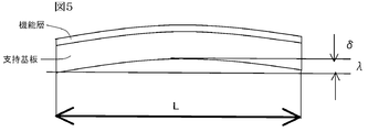
MEMSセンサの反り量λは、λ=3σ(1-ν)(H2)2L2/(4E(H1)2)で求めることが出来る。ここでσは膜応力、νは支持基板のポアソン比、H2は機能層の厚さ、Lは支持基板の長さ(直径)、Eは支持基板のヤング率、H1は支持基板の厚さである。
実験では、支持基板の厚さH1を、100μm~650μmまで50μm間隔で変化させたときに図5に示す反り量λを求めた。その実験結果を図6に示す。
図6に示すように、支持基板の厚さH1を機能層の厚さH2に対して10倍~30倍の範囲内に設定すると反り量を適切に小さくできることがわかった。ここで図6に示すように、支持基板の機能層に対する厚さ比を大きくすればするほど反り量を小さくすることができるが、あまり厚さ比を大きくしすぎるとMEMSセンサの低背化(小型化)を阻害することから上限を30倍とした。また、支持基板の厚さH1を機能層の厚さH2に対して20倍~30倍の範囲内に設定するとより好ましいと設定した。
(支持基板(第1基板)と機能層の厚さ比-アンカ部に対する応力の実験)
図7に示すシリコンからなる支持基板(第1基板)、シリコンからなる機能層、シリコンからなるキャップ基板(第2基板)を重ねた積層基板によるシミュレーション実験を行った。
図7に示すシリコンからなる支持基板(第1基板)、シリコンからなる機能層、シリコンからなるキャップ基板(第2基板)を重ねた積層基板によるシミュレーション実験を行った。
シリコンのヤング率は150GPa、ポアソン比は0.17であった。図8は図7に示す機能層の平面図である。この実験による積層基板は図3のMEMSセンサの1/2モデルである。図8に示すように、機能層は支持基板側とキャップ基板側との双方に固定支持されるアンカ部と枠体層とで構成されている。
実験では、キャップ基板の厚さH3を200μm、機能層の厚さH2を20μmに固定した。また、支持基板及びキャップ基板の幅寸法を2.5mm、幅寸法に直交する長さ寸法を0.76mmとした。
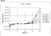
ところで、MEMSセンサには、熱応力や加工ストレス、さらには実際の使用時に力が最大で2N程度加わる。そこで、積層基板の両側を固定し、図7に示す支持基板の下面中央位置から上方に向けて(キャップ基板方向に向けて)1Nの力(実験サンプルは1/2モデルであるため半分とした)を印加した状態で、支持基板の厚さH1を、100μm、200μm、400μm、600μm、1000μmと変化させたときのアンカ部に作用する応力を求めた。その実験結果が図10に示されている。
図10に示す「位置」とは、図9に示すアンカ部の側面の支持基板(力が直接印加される側の基板)との接合位置を基準位置0とし、この基準位置0から上方に向けてのアンカ部の側面位置を指す。
図10に示すように、アンカ部に作用する最大応力は、支持基板の厚さH1が厚くなるほど小さくなっていくことがわかった。また、支持基板の各厚さH1とも、基準位置0から上方へ離れキャップ基板に近づくほど、アンカ部に作用する応力が大きくなることがわかった。
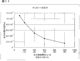
図11は、基準位置0から上方へ20μm離れた位置(キャップ基板との接合位置に相当する)でのアンカ部の最大応力を、各支持基板の厚さH1ごとにプロットしたグラフである。図11の実験結果から機能層の厚さH2(20μm)に対する支持基板の厚さH1の比を、図6の反り量の実験と同様に、10倍~30倍とすることで、アンカ部に作用する最大応力を低減できることがわかった。これにより、アンカ部の上下が基板で固定支持されたMEMSセンサの基板厚さを規制することで、外的要因等による力が加わっても、アンカ部の部分から破損する等の不具合を抑制でき、安定且つ高精度な検出特性を得ることが出来るとわかった。
(支持基板及びキャップ基板の材質と厚さの実験)
図12に示すシリコンからなる支持基板(第1基板)、シリコンからなる機能層、シリコンからなるキャップ基板(第2基板)を重ねた積層基板によるシミュレーション実験を行った。機能層は、図12に示すようにアンカ部の構造であり、支持基板側とキャップ基板側の双方に固定支持されているとする。
図12に示すシリコンからなる支持基板(第1基板)、シリコンからなる機能層、シリコンからなるキャップ基板(第2基板)を重ねた積層基板によるシミュレーション実験を行った。機能層は、図12に示すようにアンカ部の構造であり、支持基板側とキャップ基板側の双方に固定支持されているとする。
また支持基板、機能層及びキャップ基板を全てシリコンで形成した実験と、支持基板と機能層をシリコンでキャップ基板をガラスで形成した実験の双方を行った。
また、支持基板と機能層との間には酸化シリコンによる第1の接合層(厚さ1μm)が介在し、機能層とキャップ基板の間には酸化シリコンによる酸化絶縁層、アルミニウム-ゲルマニウムの第2の接合層(酸化絶縁層と第2の接合層の厚さを合わせて1μm)が介在するものとして実験を行った(構造は図2、図3参照)。
ここでシリコンの線膨張係数(22℃)を2.60×10⁻⁶、ヤング率を150GPa、ポアソン比を0.17、ガラスの線膨張係数(22℃)を3.25×10⁻⁶、ヤング率を63GPa、ポアソン比を0.25、酸化シリコンの線膨張係数(22℃)を0.56×10⁻⁶、ヤング率を72GPa、ポアソン比を0.25とした。
実験では、支持基板の厚さH1を200μmに固定し、機能層の厚さH2を20μmに固定した。また、支持基板及びキャップ基板の幅寸法を0.5mm、幅寸法に直交する長さ寸法を0.5mmとした。そして、初期状態(25℃)の歪みを0とし、±25℃の温度変化を与えながらシリコンあるいはガラスからなるキャップ基板の厚さH3を100μm、200μm、300μmと変化させたときのアンカ部のX方向(平面方向)への位置を求めた。
ここで「X方向への位置」とは、図13に示すようにアンカ部の側面の支持基板との接合位置(実際には第1の接合層との接合位置)を基準位置0とし、前記基準位置0から上方方向(キャップ基板方向への方向)に向けての各高さ位置におけるアンカ部のX方向への側面位置で示される。
アンカ部のX方向への位置と高さ位置との関係を示したのが図14である。図14に示すようにキャップ基板をガラスにするとアンカ部のX方向への位置が基準位置0から離れるほど徐々に大きくなることがわかった。また、キャップ基板をシリコンにすると多少、アンカ部のX方向への位置に変動が生じるが、キャップ基板をガラスとした場合ほどでないことがわかった。
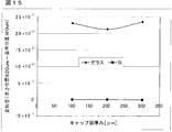
続いて上記の実験結果からキャップ基板の各厚みにおける基準位置0から20μm離れた高さ位置(キャップ基板側との接合位置)でのアンカ部のX方向への位置-基準位置0でのアンカ部のX方向への位置、すなわちアンカ部のX方向への最大変形量を求めた。その実験結果が図15に示されている。
また、図16は、キャップ基板をガラスとした場合の各キャップ基板の厚さH3に対して、基準位置0、基準位置0から10μm離れた高さ位置、基準位置0から20μm離れた高さ位置でのX方向への位置をプロットしたグラフである。
また、図17は、キャップ基板をシリコンとした場合の各キャップ基板の厚さH3に対して、基準位置0、基準位置0から10μm離れた高さ位置、基準位置0から20μm離れた高さ位置でのX方向への位置をプロットしたグラフである。
上記実験結果から、キャップ基板を支持基板と同じシリコンで形成した場合、アンカ部のX方向への変形量が非常に小さくなることがわかった。一方、キャップ基板をガラスとした場合、アンカ部のX方向への変形量は、キャップ基板をシリコンとした場合に比べて大きくなるものの、キャップ基板を支持基板と同じ200μmとした場合、最もアンカ部の変形量を小さくできることがわかった。
上記実験からキャップ基板と支持基板とを同材料で形成することが好ましいとわかった。このとき、キャップ基板と支持基板との膜厚差を100μm以内に収めることが好適であり、キャップ基板の厚さと支持基板の厚さを同じに設定することが好ましい。またキャップ基板と支持基板をシリコンで形成することが好ましい。
また、キャップ基板をガラスで形成し、支持基板をシリコンで形成し、且つ、キャップ基板と支持基板とを同厚に設定してもよいことがわかった。
以上により、熱応力に起因するアンカ部の変形量を小さくでき、安定且つ高精度な検出精度を得ることが可能になる。
H1 支持基板(第1基板)の厚さ
H2 機能層の厚さ
H3 キャップ基板(第2基板)の厚さ
1 支持基板
2 機能層
3 第1の接合層
4、16、17、18 センサ部
5,10,23,25,33,34,42,52,54 アンカ部
11 枠体層
12 キャップ部材
13 キャップ基板
14 絶縁層
15 第2の接合層
20 センサユニット
35 リード層
50 外部接続パッド
56 第1の金属層
57 第2の金属層
H2 機能層の厚さ
H3 キャップ基板(第2基板)の厚さ
1 支持基板
2 機能層
3 第1の接合層
4、16、17、18 センサ部
5,10,23,25,33,34,42,52,54 アンカ部
11 枠体層
12 キャップ部材
13 キャップ基板
14 絶縁層
15 第2の接合層
20 センサユニット
35 リード層
50 外部接続パッド
56 第1の金属層
57 第2の金属層
Claims (9)
- 第1基板と、センサ部、及び前記センサ部と一体に形成されたアンカ部を有する機能層と、前記アンカ部と前記第1基板間を接合する絶縁材料で形成された第1の接合層と、を有し、前記センサ部は前記第1基板に間隔を空けて配置されており、
前記第1基板の厚さは、前記機能層の厚さに対して10倍~30倍の範囲内で形成されることを特徴とするMEMSセンサ。 - 前記第1基板に前記機能層を介して対向する第2基板を有し、
前記センサ部は、前記第1基板及び前記第2基板と間隔を空けて配置され、前記アンカ部が、前記第2基板と第2の接合層を介して固定支持されている請求項1記載のMEMSセンサ。 - 前記第1基板と前記第2基板は、同材料で形成されている請求項2記載のMEMSセンサ。
- 前記第1基板と前記第2基板とが同厚で形成されている請求項3記載のMEMSセンサ。
- 前記第1基板と前記第2基板とがシリコンで形成されている請求項3又は4に記載のMEMSセンサ。
- 前記第1基板及び前記第2基板の一方がシリコンで他方がガラスで形成され、前記第1基板と前記第2基板とが同厚で形成されている請求項2記載のMEMSセンサ。
- 前記第2基板の前記第1基板との対向面に絶縁層が設けられ、前記第2の接合層が金属による接合層で形成されており、前記第2の接合層に接続されるリード層が前記絶縁層内に埋設されている請求項2ないし6のいずれか1項に記載のMEMSセンサ。
- 前記第2基板の前記第1基板との対向面の反対面に絶縁層が設けられ、前記第2の接合層が金属による接合層で形成されており、前記第2の接合層と前記第2基板から分離して形成された貫通配線層を介して接続されるリード層が前記絶縁層内に埋設されている請求項2ないし6のいずれか1項に記載のMEMSセンサ。
- 前記第1基板及び前記機能層が共にシリコンで形成されている請求項1ないし8のいずれか1項に記載のMEMSセンサ。
Priority Applications (1)
| Application Number | Priority Date | Filing Date | Title |
|---|---|---|---|
| JP2011503823A JPWO2010104064A1 (ja) | 2009-03-13 | 2010-03-09 | Memsセンサ |
Applications Claiming Priority (2)
| Application Number | Priority Date | Filing Date | Title |
|---|---|---|---|
| JP2009060773 | 2009-03-13 | ||
| JP2009-060773 | 2009-03-13 |
Publications (1)
| Publication Number | Publication Date |
|---|---|
| WO2010104064A1 true WO2010104064A1 (ja) | 2010-09-16 |
Family
ID=42728353
Family Applications (1)
| Application Number | Title | Priority Date | Filing Date |
|---|---|---|---|
| PCT/JP2010/053864 Ceased WO2010104064A1 (ja) | 2009-03-13 | 2010-03-09 | Memsセンサ |
Country Status (2)
| Country | Link |
|---|---|
| JP (1) | JPWO2010104064A1 (ja) |
| WO (1) | WO2010104064A1 (ja) |
Cited By (1)
| Publication number | Priority date | Publication date | Assignee | Title |
|---|---|---|---|---|
| JP2015205387A (ja) * | 2014-04-23 | 2015-11-19 | 株式会社デンソー | 物理量センサおよびその製造方法 |
Citations (7)
| Publication number | Priority date | Publication date | Assignee | Title |
|---|---|---|---|---|
| JPH11190746A (ja) * | 1997-12-25 | 1999-07-13 | Omron Corp | 半導体物理量センサ及びその製造方法 |
| JP2002273699A (ja) * | 2001-02-03 | 2002-09-25 | Robert Bosch Gmbh | マイクロメカニカル素子およびその製法 |
| JP2003039395A (ja) * | 2001-04-27 | 2003-02-13 | Hewlett Packard Co <Hp> | 懸架微細構造を形成する方法 |
| JP2004209585A (ja) * | 2002-12-27 | 2004-07-29 | Shinko Electric Ind Co Ltd | 電子デバイス及びその製造方法 |
| JP2006084326A (ja) * | 2004-09-16 | 2006-03-30 | Denso Corp | 半導体力学量センサおよびその製造方法 |
| JP2008229833A (ja) * | 2007-02-22 | 2008-10-02 | Denso Corp | 半導体装置およびその製造方法 |
| JP2008304218A (ja) * | 2007-06-05 | 2008-12-18 | Mitsubishi Electric Corp | 加速度センサおよびその製造方法 |
Family Cites Families (4)
| Publication number | Priority date | Publication date | Assignee | Title |
|---|---|---|---|---|
| US6853067B1 (en) * | 1999-10-12 | 2005-02-08 | Microassembly Technologies, Inc. | Microelectromechanical systems using thermocompression bonding |
| JP2005265565A (ja) * | 2004-03-18 | 2005-09-29 | Sony Corp | 容量検出型センサの製造方法および容量検出型センサ |
| US7238999B2 (en) * | 2005-01-21 | 2007-07-03 | Honeywell International Inc. | High performance MEMS packaging architecture |
| JP4404143B2 (ja) * | 2007-07-02 | 2010-01-27 | 株式会社デンソー | 半導体装置およびその製造方法 |
-
2010
- 2010-03-09 JP JP2011503823A patent/JPWO2010104064A1/ja active Pending
- 2010-03-09 WO PCT/JP2010/053864 patent/WO2010104064A1/ja not_active Ceased
Patent Citations (7)
| Publication number | Priority date | Publication date | Assignee | Title |
|---|---|---|---|---|
| JPH11190746A (ja) * | 1997-12-25 | 1999-07-13 | Omron Corp | 半導体物理量センサ及びその製造方法 |
| JP2002273699A (ja) * | 2001-02-03 | 2002-09-25 | Robert Bosch Gmbh | マイクロメカニカル素子およびその製法 |
| JP2003039395A (ja) * | 2001-04-27 | 2003-02-13 | Hewlett Packard Co <Hp> | 懸架微細構造を形成する方法 |
| JP2004209585A (ja) * | 2002-12-27 | 2004-07-29 | Shinko Electric Ind Co Ltd | 電子デバイス及びその製造方法 |
| JP2006084326A (ja) * | 2004-09-16 | 2006-03-30 | Denso Corp | 半導体力学量センサおよびその製造方法 |
| JP2008229833A (ja) * | 2007-02-22 | 2008-10-02 | Denso Corp | 半導体装置およびその製造方法 |
| JP2008304218A (ja) * | 2007-06-05 | 2008-12-18 | Mitsubishi Electric Corp | 加速度センサおよびその製造方法 |
Cited By (1)
| Publication number | Priority date | Publication date | Assignee | Title |
|---|---|---|---|---|
| JP2015205387A (ja) * | 2014-04-23 | 2015-11-19 | 株式会社デンソー | 物理量センサおよびその製造方法 |
Also Published As
| Publication number | Publication date |
|---|---|
| JPWO2010104064A1 (ja) | 2012-09-13 |
Similar Documents
| Publication | Publication Date | Title |
|---|---|---|
| JP5315350B2 (ja) | Memsセンサ | |
| JP2006029827A (ja) | 慣性センサ | |
| JP5175152B2 (ja) | Memsセンサ | |
| JP2005249454A (ja) | 容量型加速度センサ | |
| JP2004333133A (ja) | 慣性力センサ | |
| JP5237733B2 (ja) | Memsセンサ | |
| JP6123613B2 (ja) | 物理量センサおよびその製造方法 | |
| WO2010104064A1 (ja) | Memsセンサ | |
| JP4839826B2 (ja) | センサモジュール | |
| JP4715503B2 (ja) | センサモジュールの製造方法 | |
| KR20150082119A (ko) | Mems 센서 | |
| JP2010008172A (ja) | 半導体装置 | |
| JPWO2014042055A1 (ja) | 半導体装置 | |
| JP5033045B2 (ja) | 半導体素子の実装構造 | |
| JP2010008123A (ja) | センサモジュール | |
| JP2010107240A (ja) | 1軸加速度センサ及びそれを用いた3軸加速度センサ | |
| JP2010060464A (ja) | 物理量センサ | |
| JP4665733B2 (ja) | センサエレメント | |
| JP3938196B1 (ja) | センサモジュール | |
| JP2008008672A (ja) | 加速度センサ | |
| JP5069410B2 (ja) | センサエレメント | |
| JP4816065B2 (ja) | センサモジュールの製造方法 | |
| JP4844118B2 (ja) | センサモジュールおよびその製造方法 | |
| JP3938200B1 (ja) | センサ装置およびその製造方法 | |
| JP5547054B2 (ja) | 静電容量型加速度センサ |
Legal Events
| Date | Code | Title | Description |
|---|---|---|---|
| 121 | Ep: the epo has been informed by wipo that ep was designated in this application |
Ref document number: 10750817 Country of ref document: EP Kind code of ref document: A1 |
|
| WWE | Wipo information: entry into national phase |
Ref document number: 2011503823 Country of ref document: JP |
|
| NENP | Non-entry into the national phase |
Ref country code: DE |
|
| 122 | Ep: pct application non-entry in european phase |
Ref document number: 10750817 Country of ref document: EP Kind code of ref document: A1 |