WO2010100982A1 - 画像データ変調装置及び画像表示装置 - Google Patents
画像データ変調装置及び画像表示装置 Download PDFInfo
- Publication number
- WO2010100982A1 WO2010100982A1 PCT/JP2010/051169 JP2010051169W WO2010100982A1 WO 2010100982 A1 WO2010100982 A1 WO 2010100982A1 JP 2010051169 W JP2010051169 W JP 2010051169W WO 2010100982 A1 WO2010100982 A1 WO 2010100982A1
- Authority
- WO
- WIPO (PCT)
- Prior art keywords
- data
- image data
- bit
- frequency
- remainder
- Prior art date
- Legal status (The legal status is an assumption and is not a legal conclusion. Google has not performed a legal analysis and makes no representation as to the accuracy of the status listed.)
- Ceased
Links
Images


















Classifications
-
- G—PHYSICS
- G09—EDUCATION; CRYPTOGRAPHY; DISPLAY; ADVERTISING; SEALS
- G09G—ARRANGEMENTS OR CIRCUITS FOR CONTROL OF INDICATING DEVICES USING STATIC MEANS TO PRESENT VARIABLE INFORMATION
- G09G3/00—Control arrangements or circuits, of interest only in connection with visual indicators other than cathode-ray tubes
- G09G3/20—Control arrangements or circuits, of interest only in connection with visual indicators other than cathode-ray tubes for presentation of an assembly of a number of characters, e.g. a page, by composing the assembly by combination of individual elements arranged in a matrix no fixed position being assigned to or needed to be assigned to the individual characters or partial characters
- G09G3/2092—Details of a display terminals using a flat panel, the details relating to the control arrangement of the display terminal and to the interfaces thereto
- G09G3/2096—Details of the interface to the display terminal specific for a flat panel
-
- G—PHYSICS
- G09—EDUCATION; CRYPTOGRAPHY; DISPLAY; ADVERTISING; SEALS
- G09G—ARRANGEMENTS OR CIRCUITS FOR CONTROL OF INDICATING DEVICES USING STATIC MEANS TO PRESENT VARIABLE INFORMATION
- G09G2330/00—Aspects of power supply; Aspects of display protection and defect management
- G09G2330/06—Handling electromagnetic interferences [EMI], covering emitted as well as received electromagnetic radiation
-
- G—PHYSICS
- G09—EDUCATION; CRYPTOGRAPHY; DISPLAY; ADVERTISING; SEALS
- G09G—ARRANGEMENTS OR CIRCUITS FOR CONTROL OF INDICATING DEVICES USING STATIC MEANS TO PRESENT VARIABLE INFORMATION
- G09G2370/00—Aspects of data communication
- G09G2370/08—Details of image data interface between the display device controller and the data line driver circuit
-
- G—PHYSICS
- G09—EDUCATION; CRYPTOGRAPHY; DISPLAY; ADVERTISING; SEALS
- G09G—ARRANGEMENTS OR CIRCUITS FOR CONTROL OF INDICATING DEVICES USING STATIC MEANS TO PRESENT VARIABLE INFORMATION
- G09G3/00—Control arrangements or circuits, of interest only in connection with visual indicators other than cathode-ray tubes
- G09G3/20—Control arrangements or circuits, of interest only in connection with visual indicators other than cathode-ray tubes for presentation of an assembly of a number of characters, e.g. a page, by composing the assembly by combination of individual elements arranged in a matrix no fixed position being assigned to or needed to be assigned to the individual characters or partial characters
- G09G3/34—Control arrangements or circuits, of interest only in connection with visual indicators other than cathode-ray tubes for presentation of an assembly of a number of characters, e.g. a page, by composing the assembly by combination of individual elements arranged in a matrix no fixed position being assigned to or needed to be assigned to the individual characters or partial characters by control of light from an independent source
- G09G3/36—Control arrangements or circuits, of interest only in connection with visual indicators other than cathode-ray tubes for presentation of an assembly of a number of characters, e.g. a page, by composing the assembly by combination of individual elements arranged in a matrix no fixed position being assigned to or needed to be assigned to the individual characters or partial characters by control of light from an independent source using liquid crystals
- G09G3/3611—Control of matrices with row and column drivers
-
- G—PHYSICS
- G09—EDUCATION; CRYPTOGRAPHY; DISPLAY; ADVERTISING; SEALS
- G09G—ARRANGEMENTS OR CIRCUITS FOR CONTROL OF INDICATING DEVICES USING STATIC MEANS TO PRESENT VARIABLE INFORMATION
- G09G5/00—Control arrangements or circuits for visual indicators common to cathode-ray tube indicators and other visual indicators
- G09G5/003—Details of a display terminal, the details relating to the control arrangement of the display terminal and to the interfaces thereto
- G09G5/006—Details of the interface to the display terminal
Definitions
- the present invention relates to an image data modulation device and an image display device.
- An image display device such as a liquid crystal display, an LED display, a plasma display, a field effect display device, or an EL display includes pixels arranged in a matrix, a signal line driving circuit for supplying image signals to these pixels, And a circuit board for transmitting image data to the signal line driver circuit. The digitized image data is transmitted on the circuit board and input to the signal line driving circuit.
- digital image data input to a signal line driver circuit is 8 bits if the gradation of each pixel corresponding to a color element such as red (R), green (G), and blue (B) is 8 bits.
- X3 24-bit digital image data is transmitted.
- differential data transmission methods such as LVDS (Low Voltage Differential Signaling) and RSDS (Reduced Swing Differential Signaling) have been proposed.
- the conventional “vertical differential transmission method” has a problem that the image quality deteriorates because, for example, the N-bit image data is converted into N ⁇ 1-bit image data and then the data bit difference is taken.
- a method for solving this problem there is a method of using a remainder function to store difference data in N bits and reversibly convert it (for example, see Patent Document 2).
- the present invention provides an image data modulation device and an image display device with reduced EMI.
- a digital image data is input, a differential modulation unit that modulates a difference with respect to the previous image data delayed for a predetermined period as VDdata, and the VDdata is compressed by 1 bit using a remainder function
- a residual contracting unit that contracts the residual contracted data
- a differential signal modulating unit that modulates the residual contracted data into a serial signal, wherein the residual contracting unit has a high probability of appearance of the VDdata.
- the serial signal is converted to correspond to a small transition amount of the remainder contracted data, and the serial signal is obtained by converting the remainder contracted data for one pixel in order from the upper bit side to the lower bit side or from the lower bit side.
- an image display device comprising: a differential demodulation unit that demodulates the VDdata into digital image data.
- the “residue function” refers to a function in which N is a natural number and the digital data x corresponds to a remainder (remainder) when x is divided by 2 to the Nth power.
- the remainder may be 2 to the Nth power and may not be in the range of 0 to 2 N ⁇ 1.
- the range is not limited to 0 to 255, and may be ⁇ 128 to 127.
- residue reduction refers to digital data conversion and reduction using a remainder function
- “residue reduction data” refers to digital data converted and reduced using a residue function.
- each bit of the digital data is referred to as LSB, 1SB, 2SB, 3SB, 4SB, 5SB, 6SB, and 7SB in order from the least significant bit side, and the most significant bit is referred to as MSB.
- Invert is used for the sign or polarity of each bit, and “reverse” is used for the arrangement of a plurality of bits.
- the vertical difference (modulation) is called VD (vertical differential encoding)
- the remainder reduction is called MVD (modulo vertical differential encoding).
- an image data modulation device and an image display device with reduced EMI are provided.
- FIG. 1 is a block diagram illustrating an image data modulation device according to a first embodiment of the present invention.
- FIG. 2 is a block diagram illustrating the configuration of a vertical differential modulation unit and a residue reduction unit illustrated in FIG. 1.
- (A)-(e) is a schematic diagram explaining the principle of the remainder reduction part represented to FIG. It is a schematic diagram explaining remainder reduction data. It is a schematic diagram showing a response
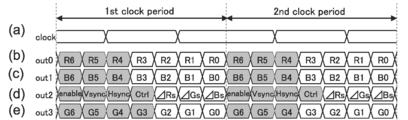
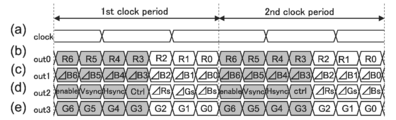
- (A) to (e) are timing charts illustrating the differential signal 54 shown in FIG.
- (A) to (c) are schematic spectrum diagrams of assumed EMI. It is a schematic diagram showing a sample image and a histogram.
- (A), (b) is a histogram of DVdata of a sample image.
- (A), (b) is the histogram of MVDdata of a sample image.
- (A), (b) is a schematic diagram showing the probability which takes 1 for every bit of the original image of a sample image, and MVDdata.
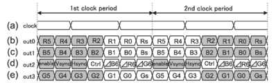
- (A) to (e) are other timing charts illustrating differential signals. It is a timing chart explaining the analysis method of a data frequency. It is a schematic diagram showing the number of bits in which 1 or 0 continues in the differential signal out0 and the frequency thereof when the original image of the sample image 1 and MVDdata are sent to the differential wiring pair.
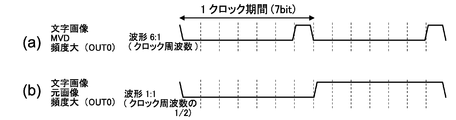
- (A), (b) is a schematic diagram showing the data with high frequency in the original image of the sample image 1, and the differential signal out0 of MVDdata.
- FIG. It is the spectrum figure after correction
- FIG. It is a far-field EMI measurement result of the original image data of the sample image 1 and MVDdata.
- FIG. 23 is a diagram showing the radiation dependence of EMI, in which the far-field EMI measurement results shown in FIG. 22 are displayed according to the order of the clock frequency. It is the spectrum figure after correction
- FIG. It is the figure which expanded and displayed the far field EMI measurement result of the original image of sample image 2, and MVDdata according to a clock frequency.
- (A) to (e) are other timing charts illustrating differential signals.
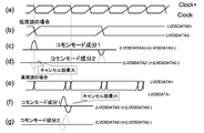
- (A)-(g) is a timing chart explaining the frequency dependence of the in-phase and anti-phase components by a differential wiring pair.
- (A) to (e) are other timing charts illustrating differential signals.
- FIG. 6 is a block diagram illustrating an image display device according to a third embodiment of the invention.
- FIG. 6 is a block diagram illustrating an image display device according to a third embodiment of the invention.
- FIG. 42 is a block diagram of a differential signal demodulator illustrated in FIG. 41. It is a block diagram which illustrates the image display apparatus which concerns on the 4th Embodiment of this invention.
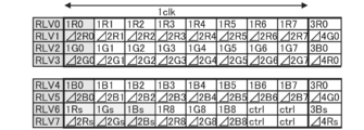
- FIG. 27 is a schematic diagram illustrating a 10-bit Mini-LVDS data mapping example corresponding to the data mapping of LVDS transmission in FIGS. 26 (a) to (e).
- FIG. 34 is a schematic diagram illustrating a 10-bit Mini-LVDS data mapping example corresponding to the data mapping of LVDS transmission in FIGS. 33 (a) to 33 (e).
- FIG. 36 is a schematic diagram illustrating a 10-bit Mini-LVDS data mapping example corresponding to the data mapping of LVDS transmission in FIGS. 35 (a) to 35 (e).
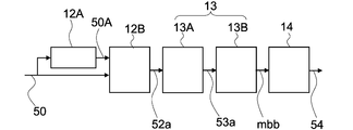
- FIG. 1 is a block diagram illustrating the configuration of an image data modulation device according to the first embodiment of the invention.
- the image data modulation device 61 of this embodiment includes a vertical differential modulation unit 12, a remainder reduction unit 13, and a differential signal modulation unit 14.
- a motion signal 54 is output.
- Digital image data 50 is modulated to VDdata 52 by the vertical differential modulation unit 12.
- the VDdata 52 is contracted to residue contract data 53 by the residue contraction unit 13, and the residue contract data 53 is modulated into a serial differential signal 54 by the differential signal modulation unit 14.
- Digital image data 50 is composed of N-bit gradation data, where N is a natural number. For example, it is sent from a graphic controller (not shown).
- the serial differential signal 54 output from the image data modulation device 61 has L M bits of serial data, where L and M are natural numbers. For example, it is sent to a display unit (not shown).
- FIG. 2 is a block diagram illustrating the configuration of the vertical differential modulation unit and the remainder reduction unit illustrated in FIG.
- the vertical differential modulation unit 12 includes a line memory 12A and a difference calculation unit 12B, inputs the digital image data 50, and outputs VDdata 52a.
- the remainder reduction unit 13 includes a residue reduction circuit 13A and a sign bit addition unit 13B, and outputs MVD data bits mbb transmitted by inputting the VDdata 52a.
- the digital image data 50 is input to the line memory 12A and the difference calculation unit 12B.
- the line memory 12A temporarily holds the image data 50, delays it for a predetermined period, and then outputs the image data (hereinafter referred to as “previous image data”) 50A held in the difference calculation unit 12B.
- image data is output with a delay of one horizontal period by the line memory 12A.
- the vertical differential transmission method based on VDdata 52a is a method that utilizes the property that the correlation in the vertical direction of images is generally high.
- the nth line image data 50 is transmitted as difference data between the nth line and the (n ⁇ 1) th line image data.
- the correlation between the image data 50 of the nth line and the previous image data 50A of the n ⁇ 1th line is high. That is, since the difference is small, the data transition is greatly reduced, so that EMI is reduced as will be described later.
- the VDdata 52a is N + 1-bit digital data.
- the VDdata 52a When the VDdata 52a is expressed by an absolute value and a sign, the data amount of one bit of the sign is increased from the digital image data 50 and becomes a value of ⁇ 255 to 255.
- the m-th image data of the n-th line is denoted by ma
- the m-th image data of the (n ⁇ 1) -th line is denoted by mb
- VDdata 52a is a value in the range of -255 to 255.
- FIGS. 3A to 3E are schematic views for explaining the principle of the remainder contraction unit shown in FIG.
- ma and mb are represented on the horizontal axis
- probability distributions P (ma) and P (mb) having certain values ma and mb are represented on the vertical axis.
- P (ma) and P (mb) having certain values ma and mb are represented on the vertical axis.
- P (ma) in which ma takes a certain value is a distribution in which the probability of taking the same value as mb is the highest from the correlation of the images in the vertical direction, and the probability decreases with increasing distance from mb.
- a remainder function of 52a is taken so that the MVD data bits mbb to be transmitted are in the range of 0 to 255.
- 53a ma-mb (mod 256)
- 53a is a residue class modulo 256 of ma-mb.
- FIG. 4 is a schematic diagram for explaining remainder reduction data.
- the OX axis is taken on a plane, and the image data ma and mb are represented by a unit length vector having a gradation value as an angle.
- the gradation values of the image data ma and mb are expressed as an angle by converting the gradation value 0 into an angle 0 and the gradation value 256 into an angle 2 ⁇ .
- any one of a1, a2 and a3 is in the range of ⁇ 128 to 127.
- a modulo circle such a display method is referred to as a modulo circle.
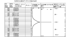
- FIG. 5 is a schematic diagram showing the correspondence between VDdata and MVDdata.
- the first column displays several examples of VDdata 52a.
- MVD data 53a (-128 to 127) is displayed in correspondence with VD data 52a.
- MVDdata reduced in the range of ⁇ 128 to 127 is represented.
- the third column displays the absolute value of MVDdata
- the fourth column displays the sign bit of MVDdata.
- the appearance probabilities of MVDdata in the natural image and the character image are schematically displayed.
- the seventh column displays the number of transition bits from zero data in MVDdata, that is, the number of 1 in the bit string of MVDdata. The fifth to seventh columns will be described later.
- data having a high appearance probability in a character image is, for example, VDdata 0, ⁇ 255, and 255. Of these, -255 and 255 have a large number of bits of “1”.
- the corresponding MVDdata is 1 and ⁇ 1, and the number of bits that are “1” is small. That is, the number of transition bits is small. In this way, the one having a large appearance probability of VDdata is converted and contracted corresponding to the one having a small transition amount of MVDdata, which contributes to the reduction of EMI, as will be described later.
- VDdata 52a and MVDdata 53a are each expressed by an absolute value and a sign bit
- 2B is a process of adding a sign bit to the least significant bit to 8 bits with respect to the 7-bit absolute value related to MVDdata 53a that is a result of the remainder reduction.
- MVDdata 53a is an MVD data value when considered in the decimal system, and when it is considered as a binary transmission signal, it is not determined which part the code bit is attached to. Therefore, when serially transmitting a transmission signal in the time direction, it is better to add code bits so that the transition probability is as small as possible.
- MVDdata 53a can take a value from -128 to 127, the absolute value of -128 is 8 bits.
- the MVD data 53a is converted to 7 bits using a method described later.
- the positive MVD data 53a corresponds to an even number
- the negative MVD data 53a corresponds to an odd number
- a sign bit is added to the LSB side of the value of absolute value data-1. This is because the absolute value in the range of ⁇ 128 to ⁇ 1 is changed to the range of ⁇ 127 to 0 and expressed by 7 bits. Even if the above operation is performed, in the MVD data 53a, 0 is (00000000) and -1 is (00000001), and can be distinguished by the sign bit.
- the relationship between VDdata 52a and MVDdata 53a can be generalized as follows.
- MVD data represents a data format in which the sign bit of MVDdata is added to the LSB side of the original 7-bit absolute value of MVDdata, that is, the MVD data bit mbb to be transmitted.
- the differential signal modulation unit 14 modulates the remainder contracted data 53 into a serial differential signal 54.
- the remaining reduced data 53 for one pixel is modulated into the differential signal 54 of L M-bit serial data (where L and M are natural numbers).
- 6A to 6E are examples, and the differential signal modulation unit 14 can also output other differential signals as described below.
- Red (red, R), green (green, G), and blue (blue, B) of the digital image data 50 are red (R7-0), green (G7-0), blue, which are 8-bit MVD data, respectively. It is reduced to (B7-0).
- red (R7-0), green (G7-0), and blue (B7-0) MVD data are arranged in order from the upper bit side to the lower bit side.
- LSB and 2SB bits data R1, G1, B1 of the second bit from the LSB side
- the image data modulation device 61 of the present embodiment is an image data modulation device for digital image data 50 that outputs such a differential signal 54.
- Arranging the image data 50 into the differential signal 54 as shown in FIGS. 6A to 6E is constructed based on the following consideration regarding EMI.
- EMI the generation principle of EMI and the reduction method thereof will be considered.
- in-phase components may occur, and as a result, EMI increases.
- VCOM occurs at the change point of the transmission signal
- the frequency of the transmission signal increases and the rate at which the in-phase component is generated increases.
- the ratio of the in-phase component to the anti-phase component becomes large, and the influence of the anti-phase component becomes relatively large. That is, the radiated electromagnetic field due to the in-phase component is measured as EMI in the high frequency region, and the radiated electromagnetic field due to the reverse phase component is measured as EMI in the low frequency region.
- V ZI.
- Z is a real number component that is an absolute value and an imaginary number component that represents a phase, and can be expressed as in equation (2).
- Z ⁇ ((R + j ⁇ L) / (G + j ⁇ C)) (2)
- the resistance R of the wiring having a rectangular parallelepiped cross section is defined as follows.
- the wiring resistivity ⁇ , the wiring width W, the wiring thickness t, and the wiring length are l.
- R ⁇ ⁇ l / w / t (4) It is expressed.
- the wiring resistance is proportional to the 1/2 power of the frequency.
- the thickness of the skin becomes thicker than the thickness of the wiring, and therefore, according to the equation (4) and according to the equation (5) at the high frequency.
- EMI is proportional to current.
- the high-frequency current component in the wiring portion is attenuated by the wiring resistance representing the conductor loss at high frequency.
- a current component passing through the differential wiring is derived from the spectrum component (FFT (Fast Fourier Transform)) of the voltage on the input side.
- FFT Fast Fourier Transform
- the radiated electric field is proportional to the FFT component obtained by converting the data waveform into the frequency component multiplied by the square root of the frequency.
- FIG. 24, FIG. 25, and FIG. 37 which will be described later, are those in which the radiation intensity is predicted by the equation (6).
- FIG. 8 is a schematic diagram showing a sample image and a histogram. As shown in FIG. 8, the sample images are two typical images, sample image 1 (character image) and sample image 2 (natural image).
- image information such as the operation screen of a personal computer is patterned, it falls into the classification of character images, and captured images such as live-action images are natural images in which adjacent image information gradually becomes brighter or darker Enter into the classification.
- FIGS. 9A and 9B are histograms of VDdata of the sample image.
- the VDdata 52a has an 8-bit notation rounded to 7-bit data obtained by removing the LSB from the absolute value and further added with a sign bit on the LSB side.
- data expressed as 254 corresponds to original data +255, that is, “11111111” in binary notation, and a positive sign bit “0” is added to the LSB side of the upper 7 bits of the original data.
- the data denoted as 255 is obtained by adding a sign bit “1” to the LSB side of the upper 7 bits of the absolute value “11111111” of the original data-255. Therefore, even numbers represent positive data and odd numbers represent negative data.
- VDdata 52a has a high probability of taking 0, and the appearance probabilities concentrate on the low gradation data values.
- the value of VDdata 52a is almost 0, but the probability of taking 254 or -255 next is high.
- VDdata 52a changes from 0 to 255 or -255, it can be seen that most data bit values rise or fall at a time.
- FIGS. 10A and 10B are MVDdata histograms of the sample image. As shown in FIGS. 10A and 10B, in the sample image 2 (natural image), the MVD data 53a has a high probability of taking 0 and is concentrated on the low gradation data value.
- the values of the MVDdata 53a corresponding to the values 254 and 255 of the VDdata 52a are “00000010” and “00000001” in binary notation, respectively. It can be seen that the number of bit transitions from 0 decreases as in the case of a natural image. Thus, in a high contrast image such as a character image, the value of VDdata 52a and the value of MVDdata 53a are greatly different.
- the fifth column and the sixth column represent the appearance probabilities of the natural image and the character image of the image signal.
- the bit values of the corresponding MVDE data 53 are shown in the third and fourth columns.
- a natural image having a high appearance probability has a high probability that the 6th and 7th bits (that is, LSB and 1SB of the absolute value data) of the absolute value of the MVDE data 53 transition from the MSB side. It can be seen that the number of bits is small. That is, the change in the absolute value of the MVD data bit is small.
- the value of MVDdata 53a has high appearance probability of “00000010” and “00000001”, and the number of bit transitions from 0 is reduced as in the natural image. That is, also in this case, the change in the absolute value of the MVD data bit is small.
- FIGS. 11A and 11B are schematic diagrams showing the probability of taking “1” for each bit of the original image of the sample image and the MVDdata.
- the probability of taking “1” for each bit of data refers to the probability that the nth bit Dn of data D will be “1”, where n is a natural number from 0 to 7, and is expressed as P1 (n) below. .
- the image data 50 and P1 (n) of the MVDdata 53a are represented with n on the horizontal axis and P1 (n) on the vertical axis.
- the probability P1 (n) of taking “1” for each bit of the MVDdata 53a in the natural image and the character image is summarized as follows.
- MVDdata 53a In each bit of the MVD data 53a, the correlation by color is high and the probability is almost the same.
- C In a character image, MVDdata 53a has a probability of taking "1" to be almost zero when n is 2 or more. In other words, in the MVD data 53a, the bits that take “1” are almost the sign bits and the LSB of the absolute value data, and the other bits remain almost “0”.
- MVDdata53a is expected to have a high EMI reduction effect.
- the differential signal 54 is the LSB and 1SB of the MVDdata 53a arranged together in out3. . Therefore, when the MVD data 53a has a configuration in which the 7 bits of the absolute value data and the 1 bit of the sign bit are arranged as described above, the probability that the sign bit of the MVD and the LSB of the absolute value data take “1” is the same. And is expected to transition in the same way. Therefore, by arranging like the out3 of this embodiment, the frequency of the differential signal can be further reduced, and the EMI can be reduced.
- EMI reduction techniques by converting the data array of MVDdata 53a can be listed as follows. Note that EMI can also be reduced by lowering the voltage of the differential signal, but here, EMI reduction methods mainly by converting the data array are listed.
- the frequency of (a) above By lowering the frequency of (a) above, the high frequency component of the spectrum V (f) of the differential signal is attenuated. Therefore, the estimated EMI spectrum obtained by multiplying the assumed EMI spectrum shown in FIGS. 7A to 7C by the voltage spectrum V (f) of the differential signal is reduced at a high frequency. In order to reduce the frequency of V (f), it is effective to reduce the frequency of data transition and lengthen the time interval of data to be transitioned.
- the magnitude of the spectrum V (f) of the differential signal can be reduced. Therefore, the spectrum of EMI is reduced.
- it is effective to associate the MVD data 53a having a small data transition amount with the VD data 52a having a high appearance frequency.
- the probability that a certain data bit takes 1 is higher than the probability that it takes 1 of lower order data bits (LSB side). Low. That is, P1 (i) ⁇ P1 (j) where 8> i> j. As a result, the amount of data transition is minimized by arranging the upper bits to the lower bits or from the lower bits to the upper bits.
- the differential signal 54 shown in FIGS. 6A to 6E also has a configuration in which data is arranged in order from the MSB to the LSB side. For example, each bit data of R7-R2, G7-G3, B7-B4 is arranged in the differential signals out0-3. Thereby, the amount of data transition is suppressed to the minimum, and the reduction of EMI is reduced.
- the spectrum V (f) of the differential signal can be changed by changing the duty ratio of (c). Thereby, for example, EMI can be reduced by reducing the spectrum V (f) of the differential signal at a specific frequency. This will be described later.
- FIGS. 12A to 12E are other timing charts illustrating differential signals.
- the differential signal modulation unit 14 modulates the residual contraction data 53 into the differential signal 54 shown in FIGS. 12A to 12E, which is the image data modulation shown in FIG. Different from the device 61. The rest is the same as that of the image data modulation device 61 shown in FIG.
- the red (red, R), green (green, G), and blue (blue, B) of the digital image data 50 are the absolute values of the MVD data bits, red (R6-0), green (G6-0), blue, respectively. (B6-0) and the sign bit, red (RS), green (GS), and blue (BS).
- the absolute values of the respective colors are arranged in order from the upper bit side to the lower bit side. Thereby, the data transition amount is suppressed to the minimum.
- the sign bits RS, GS, BS are arranged next to the control signals DE, VS, HS, CT.
- ⁇ represents bit inversion
- ⁇ RS, ⁇ GS, and ⁇ BS represent inversion of the sign bits RS, GS, and BS, respectively.
- the data values that are almost zero on the high bit side are painted in gray.
- the probability that the sign bit of the character image and the natural image is “1” is less than 0.5. Therefore, by inverting the sign bit, the probability of taking 1 becomes greater than 0.5, and the amount of data transition is reduced at the boundary between the first half control signal part and the second half sign bit part in FIG. Because it can.
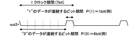
- FIG. 13 is a timing chart illustrating a data frequency analysis method.
- a continuous bit period of “1” and “0” is obtained.
- a bit period P (1) in which “1” of MVDdata continues and a bit period P (0) in which “0” continues are calculated for image data.
- the data frequency can be roughly grasped.
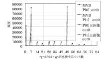
- FIG. 14 is a schematic diagram showing the number of consecutive 1 or 0 bits in the differential signal out0 and its frequency when the original image of the sample image 1 and the MVDdata are sent to the differential wiring pair.
- FIG. 14 shows the original image data in the character image and P (0) and P (1) of the differential signal out0 of MVDdata subjected to the rearrangement of FIGS. 12 (a) to 12 (e).
- FIG. 16 is a schematic diagram showing the number of consecutive 1 or 0 bits in the differential signal out2 and its frequency when the original image of the sample image 1 and the MVDdata are sent to the differential wiring pair.
- FIG. 18 is a schematic diagram showing the number of consecutive 1 or 0 bits in the differential signal out0 and its frequency when the original image of the sample image 2 and the MVDdata are sent to the differential wiring pair. That is, in FIG. 18, the original image data in the natural image and the P () of the differential signal out0 of the MVDdata (FIGS. 12A to 12E) subjected to the rearrangement of FIGS. 12A to 12E. 0) and P (1).
- FIGS. 19A and 19B are schematic diagrams showing data with high frequency in the differential signal out0 between the original image of the sample image 2 and the MVDdata. That is, a representative example of the MVDdata (FIGS. 12A to 12E) at out2 of the character image and the waveform of the original image data, which are apparent from FIG.
- the waveform can be divided into frequency components by performing FFT (Fast ⁇ Fourier ⁇ ⁇ ⁇ Transform) processing.
- the waveform can be used to estimate at which frequency the radiation increases or decreases. That is, V (f) can be calculated by performing FFT processing on the waveform data string.
- the FFT processing of the MVD data 53a as it is as described above has a large influence on the sample image, and the tendency is difficult to grasp. Therefore, the data having the highest frequency representing the characteristics of the MVD data 53a is subjected to FFT processing.
- the motif device was a liquid crystal display having a resolution of 1920 ⁇ 1080.
- EMI measurement by the 3m method is performed, and optimal rearrangement of LVDS data mapping is verified based on the actual measurement data.
- the clock frequency is 148.5 MHz, since the odd-numbered pixels and even-numbered pixels are divided, the clock frequency is 74.25 MHz.
- FIG. 20 is a spectrum diagram by FFT of MVDdata that is frequently used in the sample image 1.
- the horizontal axis represents the order N times the clock frequency, and the vertical axis represents the voltage component. Since the clock frequency is 74.25 MHz, the 13th harmonic is 965.25 MHz.
- the regulated frequency of the CISPR (International Special Committee on Radio Interference, International Radio Interference Special Committee) 22 in which the EMI limit is set is 30 MHz to 1000 MHz, so the 13th harmonic is considered.
- FIG. 21 is a spectrum diagram after correction of MVDdata that is frequently performed in the sample image 1.
- FIG. 21 shows an estimated value of the frequency dependency V (f) of the driving point voltage for comparing the MVDdata (FIGS. 12A to 12E) in the character image with the radiation intensity of the original image data.
- V (f) the frequency dependency of the driving point voltage
- FIG. 22 shows far-field EMI measurement results of the original image data of the sample image 1 and MVDdata.
- an actual LCD with a resolution of 1920 ⁇ 1080 is used, and the display image is an EMI obtained by comparing the original image with the one converted into an MVD image (FIGS. 12A to 12E) by software.
- FIG. 23 is a diagram showing the radiation dependence of EMI, which shows the far-field EMI measurement results shown in FIG. 22 according to the order of the clock frequency.
- FIG. 23 shows an EMI measurement result in which only the vicinity of the Nth harmonic component of the clock frequency is extracted in order to clarify the frequency dependence due to the waveform.
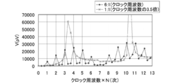
- FIG. 24 is a spectrum diagram after correction of MVDdata having a high frequency in the sample image 2.
- P (0): P (1) 1: 1 (data, which is frequently used in the original image.
- FIG. 25 is an enlarged view of the far field EMI measurement result of the original image of the sample image 2 and the MVDdata according to the clock frequency.
- ⁇ Represents the result of radiation intensity by 3m method in natural images. As expected, it is confirmed that the radiation is greatly reduced in the fourth harmonic component and that the radiation is also reduced in the sixth harmonic component.
- the EMI reduction effect in the case of MVDdata is summarized as follows.
- the image data modulation device 61 of the image data shown in FIG. 1 has an EMI reduction effect in most frequency bands. Also, it can be seen from FIGS. 21 and 24 that the differential signal arrangement shown in FIGS. 6A to 6E and FIGS. 12A to 12E is effective in reducing EMI.
- the radiation intensity may increase at the 10th and 11th harmonics of the clock frequency.
- a wire cable that transmits an LVDS signal or an FPC board has a common mode mode conversion and a large change in common mode impedance with the transmission / reception board, so that radiation increases at the resonance frequency due to the cable length. There is.
- FIGS. 26A to 26E are other timing charts illustrating differential signals. As shown in FIGS. 26A to 26E, the data arrangement order is changed between two clocks.
- the differential signal modulation unit 14 modulates the residual contraction data 53 into the differential signal 54 shown in FIGS. 26A to 26E, which is the image data modulation shown in FIG. Different from the device 61. The rest is the same as that of the image data modulation device 61 shown in FIG.
- the first clock is arranged from the lower bit to the upper bit in MVDdata, and the second clock is arranged from the upper bit to the lower bit.
- FIG. 27 is a schematic diagram showing the number of consecutive 1 or 0 bits in the differential signal out0 and the frequency thereof when the MVDdata of the sample image 2 is sent to the differential wiring section.
- P (0) and P (1) when MVDdata of a natural image is modulated into differential signals shown in FIGS. 12 (a) to (e) and FIGS. 26 (a) to (e), respectively. Represents the histogram.
- the EMI reduction effect by the adjacent data bit inversion of the differential wiring in the EMI reduction method (d) will be described.
- the differential transmission is less affected by the power supply surface and the ground surface, it may unintentionally include common mode transmission due to the waveform rising, falling imbalance, and impedance discontinuity. It will be explained that this common mode current causes a large radiation intensity when flowing into the power supply and ground plane.
- FIG. 28 is a schematic diagram showing a current distribution of adjacent differential wiring pairs in the same phase.
- FIG. 28 schematically illustrates a case where the differential wiring has two adjacent differential wirings and differential transmission paths 1 and 2 and an in-phase component is generated.
- the differential transmission path 1 includes a plus transmission line 1-1 and a minus transmission line 1-2
- the differential transmission path 2 includes a plus transmission line 2-1 and a minus transmission line. It has a line 2-2.
- each differential transmission path since the currents flowing through the pair of transmission lines are almost equal and opposite to each other, as described above, the electromagnetic field created by each transmission line cancels out with the far field and EMI is reduced.
- an imbalance may occur between the current values of the plus-side transmission lines 1-1 and 2-1 and the minus-side transmission lines 1-2 and 2-2. For example, when the data bit value is (0 ⁇ 1), the transmission lines 1-1 and 2-1 rise and the 1-2 and 2-2 fall.
- the differential transmission lines 1 and 2 both represent a state in which a high-frequency current larger than that on the minus side 1-2, 2-2 flows through the plus side transmission lines 1-1, 2-1. Yes.
- the electromagnetic field distribution at this time is as schematically shown in FIG.
- FIG. 29 the direction and magnitude of the high-frequency current of each transmission line 1-1 to 2-2 of the adjacent differential wiring pair and the direction of the electromagnetic field radiated by the high-frequency current are shown. As shown in FIG. 29, since the common mode electromagnetic field components generated by unbalance are in the same direction, they are strengthened.
- FIG. 30 is a schematic diagram illustrating a current distribution in which the adjacent differential wiring pair has a reverse phase.
- the differential wiring is different from the differential wiring shown in FIG. 28 in that a negative phase component is generated in two adjacent differential wirings and differential transmission paths 1 and 2. Other than this, the description is omitted because it is the same as FIG.
- FIG. 31 shows the direction and magnitude of the high-frequency current of each transmission line 1-1 to 2-2 of the adjacent differential wiring pair and the direction of the electromagnetic field radiated by the high-frequency current.
- the common mode electromagnetic field component generated by imbalance is in the reverse direction, it is canceled and electromagnetic waves are not transmitted to the far field.
- FIGS. 32A to 32G are timing charts for explaining the frequency dependence of the in-phase and anti-phase components due to the differential wiring pair. It represents the effect of canceling the common mode component by dephasing by the data frequency.
- 33A to 33E are other timing charts illustrating differential signals.
- 33A to 33E illustrate data mapping by rearrangement using reverse phase.
- the arrangement of signal lines shown in FIGS. 33A to 33E is effective when the data frequency is a low frequency and when it is desired to reduce a specific frequency component.
- 34A to 34E are other timing charts illustrating differential signals. 34 (a) to (e), FIGS. 26 (a) to (e) (reversing order between two clocks) and FIGS. It is a combination.
- FIGS. 35A to 35E are other timing charts illustrating differential signals.
- the sign bit (0) and the lower bit (1) are arranged in the same data string.
- the differential signal modulating unit 14 modulates the remainder contracted data 53 into the differential signal 54 shown in any one of FIGS. 33 (a) to 35 (e). Different from the image data modulation device 61 shown in FIG. The rest is the same as that of the image data modulation device 61 shown in FIG.
- the least significant bit and the sign bit have almost the same probability that the data value is 1.
- the sign bit is arranged with the least significant bit of the image bits of the differential signals out0, out1, and out3.
- the control signal of the differential signal out2 is adjacent to the upper bit, so that the transition probability can be made almost zero for both the character image and the natural image.
- FIG. 36 is a spectrum diagram after correction of MVDdata having a high frequency in the sample image 2. The result of comparing the frequency dependence after performing FFT processing on the MVD data 53a and further correcting the MVD data 53a is shown.
- FIG. 37 is an enlarged view of the far-field EMI measurement result of the original image data of the sample image 2 and the MVDdata according to the clock frequency.
- FIG. 37 the absolute values of the vertical components of the far-field radiation intensity of MVD (FIGS. 12A to 12E) and MVD (FIGS. 35A to 35E) are shown.
- radiation is reduced by the 10th harmonic component, but radiation is increased by the 6th harmonic component.
- the vertical differential modulation unit 12 modulates the image data 50 to VDdata 52 and the remainder contracting unit 13 contracts the remainder contracted data 53.
- the remainder contracting unit 13 can collectively convert the image data 50 to the remainder contracting data 53.
- FIG. 38 is a schematic diagram illustrating a processing method of the remainder contraction unit. As shown in FIG. 38, the image data mb and 128 can be compared, and the remainder contracted data mbb can be calculated according to the size.
- FIG. 39 is a schematic diagram illustrating a method for restoring MVDdata. As shown in FIG. 39, the image data mb and 128 can be compared, and the image data ma can be restored according to the size.
- FIG. 40 is a block diagram illustrating an image data modulation device according to the second embodiment of the invention. As shown in FIG. 40, in the image data modulation device 62, the digital image data 50 is collectively converted into the residual contracted data 53 by the residual contracting unit 13a. Since other than this is the same as that of the image data modulation device 61, description thereof is omitted.
- FIG. 40 illustrates a configuration in which the differential signal modulation unit 14 is used and the differential signal 54 is output in FIG. 40, but other than the differential signal 54 shown in FIGS. 6 (a) to 6 (e). 12 (a) to (e), FIGS. 26 (a) to (e), and FIGS. 33 (a) to 35 (e) may be used.
- the maximum value of EMI is reduced. Therefore, it is possible to reduce the maximum value of the desired frequency by changing the rearrangement method of the LVDS data mapping at the frequency where the radiation intensity is increased by the mounting conditions, for example, the cable length, the board frequency, and the like.
- FIG. 41 is a block diagram illustrating an image display apparatus according to the third embodiment of the invention.
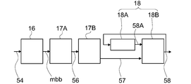
- the image display device 71 includes a graphic controller 10, an image data modulation device 61 (portion surrounded by a wavy line), a differential signal demodulation unit 16, a remainder restoration unit 17, a vertical difference demodulation unit 18, and a signal.
- a line driving circuit 20 is included. This is an image display device that converts and transmits digital image data 50 output from the graphic controller 10 and inputs the demodulated digital image data 58 to the signal line drive circuit 20 for display.
- FIG. 41 illustrates the overall configuration of an image display apparatus that employs LVDS.
- the image data modulation device 61 is the same as the image data modulation device shown in FIG.
- the digital image data 50 output from the graphic controller 10 is modulated into a serial differential signal 54 by an image data modulator 61.
- the differential signal 54 is input to the differential signal demodulator 16 by LVDS, for example, via four pairs of differential signal transmission paths. At this time, the clock signal is also transmitted to the differential signal demodulator 16 through a pair of differential signal transmission paths provided separately.
- the differential signal demodulating unit 16 demodulates the MVDdata 56 from the input serial differential signal 54 and generates timing from the clock and the control signal.
- the MVD data 56 is input to the remainder restoration unit 17 and restored to VD data 57. Restoration from MVDdata 56 to VDdata 57 is performed by taking a remainder function as described above.
- the vertical differential demodulator 18 receives the VDdata 57 and demodulates it into digital image data 58.
- the demodulated digital image data 58 is input to the signal line driving circuit 20 of the liquid crystal display unit, and an image is displayed on the liquid crystal display unit.
- the residue restoration unit 17 includes a code bit removal unit 17A and a residue restoration circuit 17B.
- the vertical differential demodulator 18 includes a line memory 18A and an adder circuit 18B, and inputs VDdata 57 and outputs digital image data 58.
- VDdata 57 is input to the line memory 18A and the addition circuit 18B.
- the line memory 18A temporarily holds the digital image data 58, delays it for a predetermined period, and then outputs the image data (hereinafter referred to as “previous image data”) 58A held in the adding circuit 18B.
- image data is output with a delay of one horizontal period by the line memory 18A.
- the remainder restoration unit 17 can collectively calculate the digital image data 58 from the MVDdata 56 based on the above-described MVDdata restoration method.
- the configuration in which the digital image data 50 is modulated into the differential signal 54 by using the image data modulation device 61 is exemplified, but the image data modulation device 62 can also be used.
- FIG. 43 is a block diagram illustrating an image display apparatus according to the fourth embodiment of the invention.
- FIG. 43 shows an image display device 72 using the image data modulation device 62 and the remainder restoration unit 18a.
- the remainder restoration unit 18a collectively converts the remainder reduction data 56 to the digital image data 58 as described above.
- the differential signal 54 in addition to using the arrangement of the remainder contracted data 53 shown in FIGS. 6A to 6E, FIGS. 12A to 12E and FIGS.
- the image data modulation apparatus using the arrangement of the remainder contraction data 53 shown in e) can also be used.
- Mini-LVDS is small-amplitude differential signal transmission used for wiring from the timing controller to the liquid crystal driver in the LCD drive board.
- 6 bits in many cases, 6 data bits are arranged in a time direction in one clock and transmitted in 3 pairs, 4 pairs, 5 pairs, or 6 pairs.
- 8 bits 8 data bits are often arranged in a time direction during one clock and transmitted in 3 pairs, 4 pairs, 5 pairs, or 6 pairs.
- 8 bits in many cases, 8 data bits are arranged in the time direction during one clock and transmitted in 6 pairs, 7 pairs, or 8 pairs.
- FIG. 44 shows a 10-bit Mini-LVDS data mapping example corresponding to the data mapping of LVDS transmission in FIGS. 26 (a) to (e).
- the code bits are arranged in the time direction and combined with a control signal with a low transition probability, but in Mini-LVDS transmission, it is combined with the most significant bit with a low transition probability.
- the code bit is serialized and combined with a data bit with a low transition probability.
- FIG. 45 shows an example of 10-bit Mini-LVDS data mapping corresponding to the data mapping of LVDS transmission in FIGS.
- the bit order of adjacent differential wirings is matched, highly related colors are arranged in adjacent differential wirings, and one of them is reversed phase.
- FIG. 46 shows a 10-bit Mini-LVDS data mapping example corresponding to the data mapping of LVDS transmission in FIGS. 35 (a) to 35 (e).
- the sign bit and the least significant bit are arranged in the time direction on the same wiring.
- the difference from FIGS. 35A to 35E is that it is not necessary to include a control signal in the data mapping, so that all the sign bits and the least significant bits of Red, Green, and Blue can be arranged on the same signal line. .
- the transition probability of the bits from the most significant bit to the lower 2 bits is low, so 6 of the 8 differential signal line pairs can be lowered in frequency, and EMI reduction can be expected.
- the wiring combining the least significant bit and the sign bit may increase the frequency, but the transition probability is not as high as that of a character image.
- the image display devices 71 and 72 of the present embodiment it is possible to reduce the EMI in the section from the image data 50 to the display unit.
- image data modulation devices and image display devices that can be implemented by those skilled in the art based on the image data modulation device and image display device described above as embodiments of the present invention are also included in the gist of the present invention. As long as they are included.
Landscapes
- Engineering & Computer Science (AREA)
- Physics & Mathematics (AREA)
- Computer Hardware Design (AREA)
- General Physics & Mathematics (AREA)
- Theoretical Computer Science (AREA)
- Control Of Indicators Other Than Cathode Ray Tubes (AREA)
- Liquid Crystal Display Device Control (AREA)
Abstract
EMIを低減した画像データ変調装置及び画像表示装置を提供する。 デジタル画像データ(50)を入力し、保持している所定の期間遅延させた前画像データに対する差分をVDdata(52)として変調する差分変調部(12)と、前記VDdataを剰余関数により1ビット圧縮した剰余縮約データ(53)に縮約する剰余縮約部(13)と、前記剰余縮約データをシリアル信号に変調する差動信号変調部(14)と、を備え、前記剰余縮約部は、前記VDdataの出現確率の大きなものを前記剰余縮約データの遷移量の小さいものに対応させて変換し、前記シリアル信号は、1画素分の前記剰余縮約データを上位ビット側から下位ビット側の順番にまたは下位ビット側から上位ビット側の順番に配列したものを有することを特徴とする画像データ変調装置が提供される。
Description
本発明は、画像データ変調装置及び画像表示装置に関する。
液晶ディスプレイやLEDディスプレイ、プラズマディスプレイ、電界効果型表示装置、ELディスプレイなどの画像表示装置は、マトリックス状に配置された画素と、これら画素に画像信号を供給するための信号線駆動回路と、この信号線駆動回路に画像データを伝送するための回路基板とを備えている。デジタル化された画像データはこの回路基板上を伝送されて、信号線駆動回路に入力される。
一般に、信号線駆動回路に入力されるデジタル画像データは、赤(R)、緑(G)、青(B)などの色要素に対応する各画素の階調が8ビットであれば、8ビット×3=24ビットのデジタル画像データが伝送される。
近年、画像表示装置の大画面化、高精細化が進められ、それに伴って、上述のような画像表示装置の回路基板上の伝送路を伝送される画像データの周波数も非常に高くなってきている。このように周波数の高いデジタルデータが伝送される場合、EMIと呼ばれる電磁ノイズが生じる場合があり、EMIを低減する必要が高まってきている。
EMIを低減する方法としては、例えば、LVDS(Low Voltage Differential Signaling)やRSDS(Reduced Swing Differential Signaling)といった差分データ伝送方式が提案されている。
しかし、近年、液晶ディスプレイなどの画像表示装置の高精細化が進み、LVDSのように小振幅差動信号に変換しても、その伝送路から発生するEMIが問題となりつつある。この問題を解決する方法の一つとして、比較的低規模な回路構成でEMIを低減する伝送方式である「垂直差分伝送方式」があり、そのデータマッピングについて提案されている(例えば、特許文献1参照)。
また、従来の「垂直差分伝送方式」では、例えば、Nビット画像データをN-1ビット画像データに変換後、データビットの差分をとるため、画質が劣化するという問題があった。この問題を解決する方法の一つとして、剰余関数を使用することにより、差分データをNビットに収め、可逆に変換する方式がある(例えば、特許文献2参照)。
本発明は、EMIを低減した画像データ変調装置及び画像表示装置を提供する。
本発明の一態様によれば、デジタル画像データを入力し、保持している所定の期間遅延させた前画像データに対する差分をVDdataとして変調する差分変調部と、前記VDdataを剰余関数により1ビット圧縮した剰余縮約データに縮約する剰余縮約部と、前記剰余縮約データをシリアル信号に変調する差動信号変調部と、を備え、前記剰余縮約部は、前記VDdataの出現確率の大きなものを前記剰余縮約データの遷移量の小さいものに対応させて変換し、前記シリアル信号は、1画素分の前記剰余縮約データを上位ビット側から下位ビット側の順番にまたは下位ビット側から上位ビット側の順番に配列したものを有することを特徴とする画像データ変調装置が提供される。
本発明の他の一態様によれば、上記の画像データ変調装置と、前記差動信号を剰余縮約データに復調する差動信号復調部と、前記剰余縮約データをVDdataに復元する剰余復元部と、前記VDdataをデジタル画像データに復調する差分復調部と、を備えたことを特徴とする画像表示装置が提供される。
なお、本願明細書において、「剰余関数」とは、Nを自然数として、デジタルデータxに、xを2のN乗で割ったときの剰余(余り)を対応させる関数をいう。例えば、9ビットの垂直差分データを28(=256)で割ったときの剰余(余り)に対応させる関数をいう。ただし、剰余は2のN乗個あればよく、0~2N-1の範囲でなくてもよい。例えば、0~255の範囲に限らず、-128~127でもよい。
また、「剰余縮約」とは、剰余関数によりデジタルデータを変換して縮約することをいい、「剰余縮約データ」とは、剰余関数により変換して縮約したデジタルデータをいう。
また、デジタルデータの各ビットを最下位ビット側から順番にLSB、1SB、2SB、3SB、4SB、5SB、6SB、7SBといい、最上位ビットをMSBという。
また、「反転」とは各ビットの符号または極性に関して用い、「逆転」とは複数のビットの配列に関して用いる。
また、垂直差分(変調)は、VD(vertical differential encoding)といい、剰余縮約は、MVD(modulo vertical differential encoding)という。
また、デジタルデータの各ビットを最下位ビット側から順番にLSB、1SB、2SB、3SB、4SB、5SB、6SB、7SBといい、最上位ビットをMSBという。
また、「反転」とは各ビットの符号または極性に関して用い、「逆転」とは複数のビットの配列に関して用いる。
また、垂直差分(変調)は、VD(vertical differential encoding)といい、剰余縮約は、MVD(modulo vertical differential encoding)という。
本発明によれば、EMIを低減した画像データ変調装置及び画像表示装置が提供される。
(第1の実施の形態)
図1は、本発明の第1の実施形態に係る画像データ変調装置の構成を例示するブロック図である。
図1に表したように、本実施例の画像データ変調装置61は、垂直差分変調部12、剰余縮約部13及び差動信号変調部14を有し、デジタル画像データ50を入力して差動信号54を出力する。
図1は、本発明の第1の実施形態に係る画像データ変調装置の構成を例示するブロック図である。
図1に表したように、本実施例の画像データ変調装置61は、垂直差分変調部12、剰余縮約部13及び差動信号変調部14を有し、デジタル画像データ50を入力して差動信号54を出力する。
デジタル画像データ50は、垂直差分変調部12によりVDdata52に変調される。VDdata52は、剰余縮約部13により剰余縮約データ53に縮約され、剰余縮約データ53は、差動信号変調部14によりシリアルの差動信号54に変調される。
デジタル画像データ50は、Nを自然数として、Nビットの階調データからなる。例えば、図示しないグラフィックコントローラなどから送られてくる。また、画像データ変調装置61から出力されるシリアルの差動信号54は、L、Mを自然数として、L本のMビットシリアルデータを有する。例えば、図示しない表示部に送られる。
次に、各部の動作を説明する。
図2は、図1に表した垂直差分変調部及び剰余縮約部の構成を例示するブロック図である。
図2に表したように、垂直差分変調部12は、ラインメモリ12A及び差分演算部12Bを有し、デジタル画像データ50を入力してVDdata52aを出力する。また、剰余縮約部13は、剰余縮約回路13A及び符号ビット付加部13Bを有し、VDdata52aを入力して伝送されるMVDデータビットmbbを出力する。
図2は、図1に表した垂直差分変調部及び剰余縮約部の構成を例示するブロック図である。
図2に表したように、垂直差分変調部12は、ラインメモリ12A及び差分演算部12Bを有し、デジタル画像データ50を入力してVDdata52aを出力する。また、剰余縮約部13は、剰余縮約回路13A及び符号ビット付加部13Bを有し、VDdata52aを入力して伝送されるMVDデータビットmbbを出力する。
デジタル画像データ50は、ラインメモリ12Aと差分演算部12Bとに入力される。
ラインメモリ12Aは、画像データ50を一旦保持し、所定の期間遅延させた後、差分演算部12Bに保持した画像データ(以下、「前画像データ」)50Aを出力する。本実施例においては、ラインメモリ12Aにより1水平期間遅延させて画像データを出力する。
ラインメモリ12Aは、画像データ50を一旦保持し、所定の期間遅延させた後、差分演算部12Bに保持した画像データ(以下、「前画像データ」)50Aを出力する。本実施例においては、ラインメモリ12Aにより1水平期間遅延させて画像データを出力する。
差分回路12Bは、デジタル画像データ50から前画像データ50Aを減算してVDdata52aを出力する。
すなわち、
nライン目のVDdata52a
=nライン目のデジタル画像データ50
-(n-1)ライン目の前画像データ50A
により、VDdata52aを出力する。1ライン目に関しては、(n-1)ライン目の前画像データ50Aが存在しないため、データ値をすべて0とする。そのため、1ライン目は元の画像データそのままが伝送される。
すなわち、
nライン目のVDdata52a
=nライン目のデジタル画像データ50
-(n-1)ライン目の前画像データ50A
により、VDdata52aを出力する。1ライン目に関しては、(n-1)ライン目の前画像データ50Aが存在しないため、データ値をすべて0とする。そのため、1ライン目は元の画像データそのままが伝送される。
VDdata52aによる垂直差分伝送方式は、一般的に画像の垂直方向の相関が高いという性質を利用した方式である。nライン目の画像データ50は、nライン目とn-1ライン目の画像データの差分データとして伝送される。nライン目の画像データ50とn-1ライン目の前画像データ50Aは相関が高い。すなわち差分が小さいため、データの遷移が大幅に減少し、そのため後述するようにEMIが低減する。
デジタル画像データ50がNビットのデジタルデータの場合、VDdata52aは、N+1ビットのデジタルデータとなる。
以下、N=8の場合を例にして説明する。デジタル画像データ50は、0~255の値となる。
以下、N=8の場合を例にして説明する。デジタル画像データ50は、0~255の値となる。
VDdata52aは、絶対値と符号とで表した場合、デジタル画像データ50よりも符号の1ビット分データ量が増え、-255から255の値となる。例えば、nライン目のm画素目の画像データをma、また、n-1ライン目のm画素目の画像データをmbとする。nライン目のm画素目のVDdata52aは、52a=ma-mbとなる。
ここで、ma、mbがそれぞれ0~255の値を取り得るため、VDdata52aは-255~255の範囲の値となる。しかし、1つのmbを固定して考えると、maは0~255の8ビット値をとるため、VDdata52a(1ライン前の画像データ)は-mbに対して52a=(0-mb)~(255-mb)の範囲の値となる。従って、VDdata52aも同様に8ビットで表せるはずである。
図3(a)~(e)は、図1に表した剰余縮約部の原理を説明する模式図である。
図3(a)~(e)においては、ma、mbを横軸に、またma、mbがある値をとる確率分布P(ma)、P(mb)を縦軸に表している。
図3(a)に表したように、mbを0~255の範囲のある1つの値に固定して考えるとP(mb)は、縦軸に平行な直線となる。maがある値をとる確率分布P(ma)は、垂直方向の画像の相関から、mbと同じ値をとる確率が最も高く、mbから離れるに従い確率が減っていく分布となる。
図3(a)~(e)においては、ma、mbを横軸に、またma、mbがある値をとる確率分布P(ma)、P(mb)を縦軸に表している。
図3(a)に表したように、mbを0~255の範囲のある1つの値に固定して考えるとP(mb)は、縦軸に平行な直線となる。maがある値をとる確率分布P(ma)は、垂直方向の画像の相関から、mbと同じ値をとる確率が最も高く、mbから離れるに従い確率が減っていく分布となる。
図3(b)に表したように、52a=ma-mbがとる確率分布P(52a)は、図3(a)のP(mb)を縦軸と一致するように並行移動した曲線となる。
ここで、図3(c)に表すように、伝送されるMVDデータビットmbbを0~255の範囲となるように、52aの剰余関数をとる。つまり、剰余縮約により、
53a=ma-mb (mod 256)
とする。ここで、53aは、ma-mbの256を法とする剰余類である。
ここで、図3(c)に表すように、伝送されるMVDデータビットmbbを0~255の範囲となるように、52aの剰余関数をとる。つまり、剰余縮約により、
53a=ma-mb (mod 256)
とする。ここで、53aは、ma-mbの256を法とする剰余類である。
このように、53aを0~255の範囲の値に制限しても、mbの値から53aの元の値を算出することができる。
53aとmbとから、maを算出する復号は、図3(d)に表したように、ma=53a+mbを算出し、さらに0~255の範囲内となるように剰余関数をとる。すなわち、
ma=53a+mb (mod 256)
とする(図3(e))。53a+mbを256で割った剰余をとればよい。
53aとmbとから、maを算出する復号は、図3(d)に表したように、ma=53a+mbを算出し、さらに0~255の範囲内となるように剰余関数をとる。すなわち、
ma=53a+mb (mod 256)
とする(図3(e))。53a+mbを256で割った剰余をとればよい。
なお、上記の剰余縮約データの算出法においては、mbbが、0~255の範囲となるように剰余縮約する場合について説明した。しかし、mbbは、任意の範囲にすることができ、例えば、-128~127の範囲にすることもできる。
その場合、剰余縮約の演算は、次のように、考えることもできる。
その場合、剰余縮約の演算は、次のように、考えることもできる。
図4は、剰余縮約データを説明する模式図である。
図4に表したように、平面上にOX軸をとり、画像データma、mbを階調値を角度とする単位長さのベクトルで表す。すなわち、画像データma、mbの階調値を、階調値0を角度0に、階調値256を角度2πに換算して、階調値を角度で表す。
図4に表したように、平面上にOX軸をとり、画像データma、mbを階調値を角度とする単位長さのベクトルで表す。すなわち、画像データma、mbの階調値を、階調値0を角度0に、階調値256を角度2πに換算して、階調値を角度で表す。
a1=ma-mb、a2=ma-mb+256、a3=ma-mb-256とおくと、a1、a2、a3のいずれかが-128~127の範囲の値となる。これを剰余縮約データmbbとする。すなわち、図4において、ma-mbを表す時計回り、反時計回りの2つの角度のうち小さい方をmbbとする。なお、このような表示法を、以下、モデュロサークルという。
図5は、VDdataとMVDdataとの対応を表す模式図である。
図5において、第1列目は、VDdata52aを数例表示している。第2列目は、MVDdata53a(-128~127)をVDdata52aに対応させて表示している。なお、ここでは、-128~127の範囲に剰余縮約したMVDdataを表している。
図5において、第1列目は、VDdata52aを数例表示している。第2列目は、MVDdata53a(-128~127)をVDdata52aに対応させて表示している。なお、ここでは、-128~127の範囲に剰余縮約したMVDdataを表している。
第3列目はMVDdataの絶対値を、また、第4列目は、MVDdataの符号ビットを表示している。また、第5列目及び6列目は、MVDdataの自然画像及び文字画像における出現確率をそれぞれ模式的に表示している。さらに、第7列目は、MVDdataにおけるゼロデータからの遷移ビット数、つまりMVDdataのビット列の1の数を表示している。なお、第5~7列目については、後述する。
図5に表したように、文字画像における出現確率の高いデータは、例えば、VDdataの0、-255、255である。このうち、-255と255とは、”1”となっているビット数が多い。これに対して、対応するMVDdataは、1と-1で、”1”となっているビット数が少ない。すなわち、遷移ビット数が少ない。
このように、VDdataの出現確率の大きなものを、MVDdataの遷移量の小さいものに対応させて変換して縮約する、これは、後述するように、EMIの低減に寄与する。
このように、VDdataの出現確率の大きなものを、MVDdataの遷移量の小さいものに対応させて変換して縮約する、これは、後述するように、EMIの低減に寄与する。
なお、VDdata52a及びMVDdata53aを、それぞれ絶対値と符号ビットとで表す場合は、絶対値データのLSB側に符号ビットを追加した表記を用いる。図2の13Bは、剰余縮約した結果であるMVDdata53aに関する7bitの絶対値に対して、符号ビットをさらに最下位ビットに付加して8bitとするプロセスである。すなわち、MVDdata53aは10進法で考えた場合のMVDデータ値であり、2進法の伝送信号で考えた場合、符号ビットをどの部分につけるかは決まっていない。そこで、伝送信号を時間方向にシリアル伝送する場合に、なるべく遷移確率が少なくなるように符号ビットを付加する方がよい。また、MVDdata53aは-128から127の値をとりうるため、-128に関してはその絶対値が8bitとなっている。MVDdata53aは後述の方法を用いて7ビット化する。
従って、プラスのMVDdata53aは偶数に対応し、マイナスのMVDdata53aは奇数に対応することになる。ただし、マイナスデータに対しては、絶対値データ-1の値のLSB側に符号ビットを追加した表記とする。-128~-1の範囲の絶対値を-127~0の範囲へ変更し、7ビットで表すためである。上記の操作を行っても、MVDdata53aにおいて、0は(00000000)、-1は(00000001)で符号ビットにより区別ができる。
例えば、MVDdata53aの1は、2進表記の絶対値=”0000001”のLSB側に符号ビット”0”を追加して”00000010”となる。また、MVDdata53aの-1は、2進表記の絶対値-1=”0000000”のLSB側に符号ビット”1”を追加して”00000001”となる。なお、VDdata52aとMVDdata53aとの関係を以下のように一般化することができる。
if a<=-2^(N-1)-1
b=a+2^N
else if a>=2^(N-1)
b=a-2^N
else
b=a
b=a+2^N
else if a>=2^(N-1)
b=a-2^N
else
b=a
10bitの場合
if a<=-513
b=a+1024
else if a>=512
b=a-1024
else
b=a
if a<=-513
b=a+1024
else if a>=512
b=a-1024
else
b=a
8bitの場合
if a<= -129
b=a+256
else if a>=128
b=a-256
else
b=a
if a<= -129
b=a+256
else if a>=128
b=a-256
else
b=a
また、MVDdata53aとmbbとの関係を以下のように一般化することができる。
if 53a<0
mbb=-(53a+1)×2+1
if 53a>=0
mbb=53a×2
if 53a<0
mbb=-(53a+1)×2+1
if 53a>=0
mbb=53a×2
以下、単にMVDデータという場合は、もとのMVDdataの絶対値7ビットのLSB側に、MVDdataの符号ビットを追加したデータ形式、すなわち伝送されるMVDデータビットmbbを表すものとする。
ここで、図1に戻り、差動信号変調部14について説明する。
差動信号変調部14は、剰余縮約データ53をシリアル信号の差動信号54に変調する。上記のとおり、1画素分の剰余縮約データ53を、L本のMビットシリアルデータの差動信号54に変調する(ただし、L、Mは自然数)。
差動信号変調部14は、剰余縮約データ53をシリアル信号の差動信号54に変調する。上記のとおり、1画素分の剰余縮約データ53を、L本のMビットシリアルデータの差動信号54に変調する(ただし、L、Mは自然数)。
図6(a)~(e)は、図1に表した差動信号54を例示するタイミングチャートである。
図6(a)~(e)に表したように、本実施例においては、L=4、M=7の場合を例示している。
図6(a)は、クロックclockを表す。また1クロック周期に、図6(b)out0、(c)out1、(d)out2、(e)out3に表したように、L×M=4×7=28ビットの1画素分のデータおよび制御データを伝送する。なお、図6(a)~(e)は例示であり、以下に説明するように、差動信号変調部14は、他の差動信号を出力することもできる。
図6(a)~(e)に表したように、本実施例においては、L=4、M=7の場合を例示している。
図6(a)は、クロックclockを表す。また1クロック周期に、図6(b)out0、(c)out1、(d)out2、(e)out3に表したように、L×M=4×7=28ビットの1画素分のデータおよび制御データを伝送する。なお、図6(a)~(e)は例示であり、以下に説明するように、差動信号変調部14は、他の差動信号を出力することもできる。
デジタル画像データ50は、本実施例においては、N=8ビット階調である。デジタル画像データ50の赤(red、R)、緑(green、G)、青(blue、B)は、それぞれ8ビットのMVDデータである赤(R7~0)、緑(G7~0)、青(B7~0)に縮約されている。
また、赤(R7~0)、緑(G7~0)、青(B7~0)のMVDデータは、それぞれ上位ビット側から下位ビット側の順番に配列されている。なお、LSB及び2SB(LSB側から2ビット目のビットデータR1、G1、B1)は、まとめて差動信号out3に配列されている。これについては、後述する。
本実施例の画像データ変調装置61は、このような差動信号54を出力するデジタル画像データ50の画像データ変調装置である。
図6(a)~(e)に表したように画像データ50を差動信号54に配列することは、EMIに関する以下の考察に基づいて構築されたものである。
ここで、EMIの発生原理及びその低減方法について考察する。
図6(a)~(e)に表したように画像データ50を差動信号54に配列することは、EMIに関する以下の考察に基づいて構築されたものである。
ここで、EMIの発生原理及びその低減方法について考察する。
差動配線においても、同相成分が発生する場合があり、その結果、EMIが大きくなる。同相成分VCOMが伝送信号の変化点で生じる場合、伝送信号の周波数が高くなるとともに、同相成分の発生する割合が増加する。同相成分の逆相成分に対する比が大きくなり、相対的に逆相成分の影響が大きくなる。つまり、高周波数の領域においては、同相成分による放射電磁界が、また低周波数の領域においては、逆相成分による放射電磁界がEMIとし測定されると考えられる。
従って、差動配線に周波数fの電流Iを流した場合の、遠方における放射電磁界EMIは、(1)式で与えられる。すなわち、十分遠方では、同相の微小電流による電界Eは、透磁率をμ、アンテナと差動配線の中央部との距離をdとすると、電流の周波数f、電流の長さs、電流の大きさIに比例する。
E(f)=μfsI/d ・・・(1)
E(f)=μfsI/d ・・・(1)
差動配線の電圧と電流の関係式はV=ZIで表わされる。
ここで、Zは絶対値である実数成分と位相を表わす虚数成分で(2)式のように表わすことができる。
Z=√((R+jωL)/(G+jωC)) ・・・(2)
ここで、Zは絶対値である実数成分と位相を表わす虚数成分で(2)式のように表わすことができる。
Z=√((R+jωL)/(G+jωC)) ・・・(2)
表皮の厚さδと周波数fの関係は、(3)式で与えられる。
δ=√(2ρ/(ωμ))=√(ρ/(πfμ)) ・・・(3)
δ=√(2ρ/(ωμ))=√(ρ/(πfμ)) ・・・(3)
断面形状が直方体の配線の抵抗Rは、配線の抵抗率ρ、配線幅W、配線の厚みt、配線の長さをlとすると、
R=ρ×l/w/t ・・・(4)
と表される。ここで、表皮の厚さδが薄くなると、配線の中を流れる電流の厚みtが薄くなる。そのため、配線抵抗が周波数の1/2乗に比例することを示す。数十MHzでの配線部の厚みtと、表皮の厚さが同程度の厚さになった時の抵抗値をRo とすると
t(f)=Ro /√f
R(f)=ρ×l/w/(Ro /√f)
=ρ×l/w/Ro*√f ・・・(5)
R=ρ×l/w/t ・・・(4)
と表される。ここで、表皮の厚さδが薄くなると、配線の中を流れる電流の厚みtが薄くなる。そのため、配線抵抗が周波数の1/2乗に比例することを示す。数十MHzでの配線部の厚みtと、表皮の厚さが同程度の厚さになった時の抵抗値をRo とすると
t(f)=Ro /√f
R(f)=ρ×l/w/(Ro /√f)
=ρ×l/w/Ro*√f ・・・(5)
ここで、周波数が十分低い時には、表皮の厚みが配線の厚みより厚くなるため、(4)式に従い、高周波では、(5)式に従う。
EMIは、電流に比例する。また、高周波での導体損を表す配線抵抗により、配線部の高周波電流成分は減衰する。
EMIは、電流に比例する。また、高周波での導体損を表す配線抵抗により、配線部の高周波電流成分は減衰する。
入力側の電圧のスペクトル成分(FFT(Fast Fourier Transform))より、差動配線を通過する電流成分を導出する。
上記の配線抵抗R(f)を持つ配線に電圧Vをかけると、電流Iは以下のようになる。
I=V(f)/R(f)=V/(ρ×l/w/(Ro /√f))
=V(f)×w×Ro/ρ/l/√f
となる。
上記の配線抵抗R(f)を持つ配線に電圧Vをかけると、電流Iは以下のようになる。
I=V(f)/R(f)=V/(ρ×l/w/(Ro /√f))
=V(f)×w×Ro/ρ/l/√f
となる。
ここで、EMIが、高周波の同相成分で、(1)式に従うとすると、
E(f)=μfsI/d
∝fsV(f)/d/√f
∝√fsV(f)/d ・・・(6)
となる。
E(f)=μfsI/d
∝fsV(f)/d/√f
∝√fsV(f)/d ・・・(6)
となる。
このように、放射電界は、データ波形を周波数成分に変換したFFT成分に周波数の平方根をかけたものに比例する。後に述べる図23、図24、図25、図37のEMIは(6)式により放射強度を予測したものである。
デジタル画像データ50の統計的性質を把握するために、画像全画面で、データ値が連続するビット数を集計する。
図8は、サンプル画像とヒストグラムを表す模式図である。
図8に表したように、サンプル画像は、典型的な2種類の画像、サンプル画像1(文字画像)とサンプル画像2(自然画像)である。
図8は、サンプル画像とヒストグラムを表す模式図である。
図8に表したように、サンプル画像は、典型的な2種類の画像、サンプル画像1(文字画像)とサンプル画像2(自然画像)である。
これらの画像を例として、図1に表したような画像データ50から差動信号54へのデータ処理を行う。パソコンの操作画面のような画像情報は、パターン化されているため、文字画像の分類に入り、実写等の撮影画像は、隣接画像情報が徐々に明るくなったり、暗くなったりするような自然画像の分類に入る。
図9(a)、(b)は、サンプル画像のVDdataのヒストグラムである。
ここで、VDdata52aは、その絶対値からLSBを除いた7ビットのデータに丸め、さらにLSB側に符号ビットを追加した8ビット表記となっている。
ここで、VDdata52aは、その絶対値からLSBを除いた7ビットのデータに丸め、さらにLSB側に符号ビットを追加した8ビット表記となっている。
例えば、254と表記されたデータは、元データ+255、つまり2進表記で”11111111”に対応し、元データの上位7ビットのLSB側に、正の符号ビット”0”を追加したものである。同様に、255と表記されたデータは、元データ-255の絶対値”11111111”の上位7ビットのLSB側に符号ビット”1”を追加したものである。従って、偶数は正データを、奇数は負データを表す。
図9(a)、(b)に表したように、サンプル画像2(自然画像)において、VDdata52aは0をとる確率が高く、出現確率が低階調データ値に集中することがわかる。
また、サンプル画像1(文字画像)においては、VDdata52aの値は、ほとんどが0をとるが、その次に、254、あるいは-255をとる確率が高い。
また、サンプル画像1(文字画像)においては、VDdata52aの値は、ほとんどが0をとるが、その次に、254、あるいは-255をとる確率が高い。
すなわち、VDdata52aの値は、0から255または-255に変化する場合、ほとんどのデータビット値が一度に立ち上がる、あるいは立ち下がることがわかる。
図10(a)、(b)は、サンプル画像のMVDdataのヒストグラムである。
図10(a)、(b)に表したようにサンプル画像2(自然画像)において、MVDdata53aは0をとる確率が高く、低階調データ値に集中することがわかる。
図10(a)、(b)に表したようにサンプル画像2(自然画像)において、MVDdata53aは0をとる確率が高く、低階調データ値に集中することがわかる。
また、サンプル画像1(文字画像)においては、VDdata52aの値254、255に対応するMVDdata53aの値は、それぞれ2進表記で”00000010”、”00000001”となる。0からのビット遷移の数が自然画像と同様少なくなることがわかる。このように、文字画像のようなコントラストの高い画像において、VDdata52aの値とMVDdata53aの値が大きく異なる。
ここで、図5に戻り、VDdata52aとMVDdata53aとの対応関係をみる。
第5列目及び第6列目に、画像信号の自然画像、文字画像の出現確率を表している。また、対応するMVDEデータ53のビット値を第3列目、第4列目に表している。
第5列目及び第6列目に、画像信号の自然画像、文字画像の出現確率を表している。また、対応するMVDEデータ53のビット値を第3列目、第4列目に表している。
自然画像で出現確率が高いものは、MVDEデータ53の絶対値のうち、MSB側から数えて6ビット目、7ビット目(つまり絶対値データのLSB及び1SB)が遷移する確率が高く、遷移するビットの数が少ないことがわかる。つまり、MVDデータビットの絶対値の変化は小さい。
また、上記のとおり、文字画像においては、MVDdata53aの値が、”00000010”、”00000001”の出現確率が高く、0からのビット遷移の数が自然画像と同様少なくなることがわかる。つまり、この場合もMVDデータビットの絶対値の変化が小さい。
図11(a)、(b)は、サンプル画像の元画像及びMVDdataのビットごとの”1”をとる確率を表す模式図である。ここで、データのビットごとの”1”をとる確率とは、nを0~7の自然数として、データDのnビット目Dnが”1”になる確率をいい、以下P1(n)と表す。
図11(a)、(b)においては、nを横軸に、P1(n)を縦軸にとって、画像データ50及びMVDdata53aのP1(n)を表している。
図11(a)、(b)から、自然画像、文字画像におけるMVDdata53aのビットごとの”1”をとる確率P1(n)について、以下のようにまとめられる。
図11(a)、(b)から、自然画像、文字画像におけるMVDdata53aのビットごとの”1”をとる確率P1(n)について、以下のようにまとめられる。
(ア)自然画像のMVDdata53aの値においては、ビット値nが0から7に増大するに従い、”1”をとる確率P1(n)が減り、nが4以上で0.1以下となる。符号ビットとMVDデータビットの絶対値データのLSBとは、”1”をとる確率がほぼ同程度となる。
(イ)MVDdata53aの各ビットにおいて、色による相関が高く、ほぼ同一の確率となる。
(ウ)文字画像においては、MVDdata53aは、nが2以上のとき、”1”をとる確率がほぼ0となる。つまり、MVDdata53aにおいては、”1”をとるビットは、ほぼ符号ビットと絶対値データのLSBとであり、他のビットはほぼ”0”のままである。
(ウ)文字画像においては、MVDdata53aは、nが2以上のとき、”1”をとる確率がほぼ0となる。つまり、MVDdata53aにおいては、”1”をとるビットは、ほぼ符号ビットと絶対値データのLSBとであり、他のビットはほぼ”0”のままである。
このように、MVDdata53aにおいては、デジタル画像データ50及びVDdata52aと比較して、データビットの遷移が少ない。そのため、MVDdata53aは、EMI低減効果が高いことが予想される。
ここで、図6(a)~(e)に戻ると、本実施例の画像データ変調装置61においては、差動信号54を、MVDdata53aのLSBと1SBとを、まとめてout3に配列している。そこで、MVDdata53aが、絶対値データの7ビットと符号ビット1ビットとを上記のように配置した構成の場合は、MVDの符号ビットと絶対値データのLSBとは、”1”をとる確率が同程度であり、同じように遷移すると予想される。従って、本実施例のout3のように配列することにより、差動信号の周波数をさらに低減することができ、EMIを低減することができる。
文字画像、自然画像におけるMVDdata53aの特徴は、上記のとおりである。
これらのデータビットの傾向をもとに、MVDdata53aのデータ配列を変換することによるEMI低減手法が以下のように列挙できる。なお、差動信号の電圧を低電圧化することによっても、EMIを低減できるが、ここでは、主にデータ配列を変換ことによるEMIの低減手法を列挙する。
これらのデータビットの傾向をもとに、MVDdata53aのデータ配列を変換することによるEMI低減手法が以下のように列挙できる。なお、差動信号の電圧を低電圧化することによっても、EMIを低減できるが、ここでは、主にデータ配列を変換ことによるEMIの低減手法を列挙する。
(a)低周波化する。
(b)データ遷移量を減少する。
(c)デューティ比を変化させて放射周波数を変化する。
(d)隣接差動配線の逆相化をする。
(b)データ遷移量を減少する。
(c)デューティ比を変化させて放射周波数を変化する。
(d)隣接差動配線の逆相化をする。
上記(a)の低周波化することにより、差動信号のスペクトルV(f)の高周波成分が減衰する。そのため、図7(a)~(c)に表した想定されるEMIのスペクトルに差動信号の電圧スペクトルV(f)を乗算した推定EMIのスペクトルが高周波数で低減される。
V(f)を低周波数化するには、データ遷移の頻度を減少すること、及び遷移するデータの時間間隔を長くすることが有効である。
V(f)を低周波数化するには、データ遷移の頻度を減少すること、及び遷移するデータの時間間隔を長くすることが有効である。
(b)のデータ遷移量を減少することにより、差動信号のスペクトルV(f)の大きさを減少することができる。そのため、EMIのスペクトルが低減される。
データ遷移量を減少するためには、出現頻度の高いVDdata52aにデータ遷移量の少ないMVDdata53aを対応させるのが有効である。
データ遷移量を減少するためには、出現頻度の高いVDdata52aにデータ遷移量の少ないMVDdata53aを対応させるのが有効である。
また、基本的な手法として、図11(a)、(b)に表したように、あるデータビットが1をとる確率は、それより低い次数(LSB側)のデータビットの1をとる確率より低い。つまり、8>i>jとして、P1(i)<P1(j)である。これより、上位ビットから下位ビット、あるいは下位ビットから上位ビットへ並べることにより、データ遷移量が最小限に抑制される。
図6(a)~(e)に表した差動信号54においても、MSBからLSB側の順番にデータを配列した構成となっている。例えば、R7-R2、G7-G3、B7-B4の各ビットデータを差動信号out0~3に配列している。これにより、データ遷移量が最小限に抑制され、EMIを低減が低減される。
(c)のデューティ比を変化させて差動信号のスペクトルV(f)を変化させることができる。これにより、例えば、特定の周波数における差動信号のスペクトルV(f)を低減することにより、EMIを減少させることができる。なお、これについては、後述する。
(d)の隣接差動配線の逆相化をすることにより、同相成分をキャンセルして、EMIを低減することができる。差動信号が逆相成分の場合は、推定されるEMIのスペクトルは周波数fの2乗で減少するため、EMIを大きく低減することができる。なお、これについては後述する。
次に、上記(c)のデューティ比を変化させて差動信号のスペクトルV(f)を変化させることについて説明する。
図12(a)~(e)は、差動信号を例示する他のタイミングチャートである。
本実施例においては、差動信号変調部14は、剰余縮約データ53を図12(a)~(e)に表した差動信号54に変調する点が、図1に表した画像データ変調装置61と異なる。これ以外は、図1に表した画像データ変調装置61と同様であるので説明を省略する。
図12(a)~(e)は、差動信号を例示する他のタイミングチャートである。
本実施例においては、差動信号変調部14は、剰余縮約データ53を図12(a)~(e)に表した差動信号54に変調する点が、図1に表した画像データ変調装置61と異なる。これ以外は、図1に表した画像データ変調装置61と同様であるので説明を省略する。
デジタル画像データ50は、本実施例においては、N=8ビット階調である。デジタル画像データ50の赤(red、R)、緑(green、G)、青(blue、B)は、それぞれMVDデータビットの絶対値、赤(R6~0)、緑(G6~0)、青(B6~0)及び符号ビット、赤(RS)、緑(GS)、青(BS)に縮約されている。
また、図12(a)~(e)に表したように、差動信号out0、1、3においては、各色の絶対値を上位ビット側から下位ビット側の順番に配列している。これにより、データ遷移量が最小限に抑制される。
さらに、差動信号out2において、制御信号DE、VS、HS、CT、の次に符号ビットRS、GS、BSを配列している。なお、Δは、ビット反転を表し、ΔRS、ΔGS、ΔBSは、それぞれ、符号ビットRS、GS、BSの反転を表している。なお、図12(a)~(e)においては、高ビット側でデータ値がほとんど0となるものを灰色で塗りつぶしている。
さらに、差動信号out2において、制御信号DE、VS、HS、CT、の次に符号ビットRS、GS、BSを配列している。なお、Δは、ビット反転を表し、ΔRS、ΔGS、ΔBSは、それぞれ、符号ビットRS、GS、BSの反転を表している。なお、図12(a)~(e)においては、高ビット側でデータ値がほとんど0となるものを灰色で塗りつぶしている。
図12(a)~(e)に表したように、符号ビットを他の画像ビットのデータ列と分離し、制御信号と同一線路におくことにより、データ遷移確率の高いビットが並ばないため、高周波成分を除去することができる。さらに、制御信号と符号ビットを同一線路におくことにより、制御信号がほぼ一定の値をとるため、データ周波数の高周波成分を低減することができる。
また、図11(a)、(b)に表したように文字画像、自然画像の符号ビットが”1”をとる確率は、0.5より小さい。そのため、符号ビットを反転させることにより、1をとる確率が0.5より大きくなり、図12(d)out2の前半の制御信号部、後半の符合ビット部の境界部でデータ遷移量を少なくすることができるからである。
ところで、時間データのMVDdata53aからそのままFFTなどによりスペクトル成分を算出することは、サンプル画像の影響が大きく、傾向がつかみにくい。そこで、まずMVDdata53aの特徴を表す最高頻度を持つデータを抽出することにする。
図13は、データ周波数の分析方法を説明するタイミングチャートである。
画像データのデータ波形の周波数、すなわち、差動配線を駆動する電圧V(f)を把握するために、”1”及び”0”の連続するビット期間を求める。
図13に表したように、MVDdataの”1”が連続するビット期間P(1)、及び”0”が連続するビット期間P(0)を画像データについて算出する。図13においては、P(1)=1、P(0)=6の場合を例示している。
画像データのデータ波形の周波数、すなわち、差動配線を駆動する電圧V(f)を把握するために、”1”及び”0”の連続するビット期間を求める。
図13に表したように、MVDdataの”1”が連続するビット期間P(1)、及び”0”が連続するビット期間P(0)を画像データについて算出する。図13においては、P(1)=1、P(0)=6の場合を例示している。
P(1)とP(0)の多いビット期間を組み合わせることにより、データ周波数をおよそ把握することができる。例えば、上記の場合、データ周期は、P(1)+P(0)=7bitであり、デューティ比=(パルス幅)/(データ周期)=1/7となる。
図14は、サンプル画像1の元画像及びMVDdataを差動配線対に送った場合の差動信号out0における1または0が連続するビット数とその頻度を表す模式図である。
図14においては、文字画像における元画像データと、図12(a)~(e)の並び替えを施したMVDdataの差動信号out0のP(0)とP(1)とを表している。
図14においては、文字画像における元画像データと、図12(a)~(e)の並び替えを施したMVDdataの差動信号out0のP(0)とP(1)とを表している。
MVDdata(図12(a)~(e))はクロック周波数と同一の7bit区間の周期で、P(0):P(1)=6:1の頻度が多い。一方、元画像データは、周期はクロック周波数の8倍の56bit区間の周期で、P(0):P(1)=7:49の頻度が多い。そのため、差動信号out2では、並び替えにより、データ周波数は高周波化している。
ここで、文字画像において、高精細な文字が多い場合は1画素ごとに、白と黒が切り替わるため、文字画像の元画像としては、14ビット区間の周期で、P(0):P(1)=7:7の頻度も多くなる可能性が大きい。
ここで、文字画像において、高精細な文字が多い場合は1画素ごとに、白と黒が切り替わるため、文字画像の元画像としては、14ビット区間の周期で、P(0):P(1)=7:7の頻度も多くなる可能性が大きい。
図15(a)、(b)は、サンプル画像1の元画像及びMVDdataとの差動信号out0における頻度の多いデータを表す模式図である。
頻度を比較すると、MVDdata(図12(a)~(e))における7ビット区間の周期の頻度:元画像における56ビット区間の周期の頻度=25000:80000=5:16と、元画像データに比較してデータ遷移量は減少している。
上記より、MVDにより、データ遷移量は減少しているが、文字画像の場合、ひとつの配線のみを注目するとデータ周波数が高周波化していることがある。
頻度を比較すると、MVDdata(図12(a)~(e))における7ビット区間の周期の頻度:元画像における56ビット区間の周期の頻度=25000:80000=5:16と、元画像データに比較してデータ遷移量は減少している。
上記より、MVDにより、データ遷移量は減少しているが、文字画像の場合、ひとつの配線のみを注目するとデータ周波数が高周波化していることがある。
図16は、サンプル画像1の元画像及びMVDdataを差動配線対に送った場合の差動信号out2における1または0が連続するビット数とその頻度を表す模式図である。
MVDdata(図12(a)~(e))はクロック周波数と同一の7ビット区間の周期で、P(0):P(1)=3:4の頻度が多い。一方、元画像データはクロック周波数の8倍の7ビット区間の周期で、P(0):P(1)=4:3の頻度が多い。そのため、差動信号out2では、並び替えにより、データ周波数は変化していない。
MVDdata(図12(a)~(e))はクロック周波数と同一の7ビット区間の周期で、P(0):P(1)=3:4の頻度が多い。一方、元画像データはクロック周波数の8倍の7ビット区間の周期で、P(0):P(1)=4:3の頻度が多い。そのため、差動信号out2では、並び替えにより、データ周波数は変化していない。
図17は、サンプル画像1の元画像及びMVDdataとの差動信号out2における頻度の多いデータを表す模式図である。
頻度を比較すると、MVDdata(図12(a)~(e))における7ビット区間の周期の頻度:元画像データにおける56ビット区間の周期の頻度=24000:48000=1:2と、元画像データに比較してMVDdata(図12(a)~(e))は、データ遷移量は減少している。
頻度を比較すると、MVDdata(図12(a)~(e))における7ビット区間の周期の頻度:元画像データにおける56ビット区間の周期の頻度=24000:48000=1:2と、元画像データに比較してMVDdata(図12(a)~(e))は、データ遷移量は減少している。
図18は、サンプル画像2の元画像及びMVDdataを差動配線対に送った場合の差動信号out0における1または0が連続するビット数とその頻度を表す模式図である。
すなわち、図18においては、自然画像における元画像データと、図12(a)~(e)の並び替えを施したMVDdata(図12(a)~(e))の差動信号out0のP(0)とP(1)とを表している。
すなわち、図18においては、自然画像における元画像データと、図12(a)~(e)の並び替えを施したMVDdata(図12(a)~(e))の差動信号out0のP(0)とP(1)とを表している。
MVDdata(図12(a)~(e))はクロック周波数と同一の7ビット区間の周期で、P(0):P(1)=6:1の頻度が多い。一方、元画像データは1ビット周期で変動するため、クロック周波数の周期より短く、周波数としては、3.5倍、1.75倍とクロック周波数よりも高い周波数成分を持つ。すなわち、高い周波数の方で、1:1、1:2、2:2、1:3、3:2・・・というデューティ比を持つ。しかし、最高頻度をもつものとしては、P(0):P(1)=1:1となる。
図19(a)、(b)は、サンプル画像2の元画像及びMVDdataとの差動信号out0における頻度の多いデータを表す模式図である。
すなわち、図18から明らかになった文字画像のout2におけるMVDdata(図12(a)~(e))と元画像データの波形の代表例を表している。
すなわち、図18から明らかになった文字画像のout2におけるMVDdata(図12(a)~(e))と元画像データの波形の代表例を表している。
頻度を比較すると、MVDdata(図12(a)~(e))における7ビット区間の周期の頻度:元画像データにおける2ビット区間の周期の頻度=200000:900000=2:9と、元画像データに比較して、自然画像においてもMVDdata(図12(a)~(e))はデータ遷移量が大きく減少している。
上記より、MVDdata53aにより、自然画像はデータ遷移量も低減し、データ周波数も低周波化するため、EMIの放射低減が成される要因が(a)、(b)の2項目存在する。
画像分析により、MVDdata53aと元画像データ50の文字画像における頻度の高いデューティ比が異なることがわかった。波形にFFT(Fast Fourier Transform)処理することにより、周波数成分に分けることができる。波形により、どの周波数で放射が増大、あるいは低減するかを見積もることができる。すなわち、波形のデータ列をFFT処理することにより、V(f)を算出することができる。
なお、上記のとおりMVDdata53aをそのままFFT処理することは、サンプル画像の影響が大きく、傾向がつかみにくい。そこで、MVDdata53aの特徴を表す最高頻度を持つデータをFFT処理することにする。
モチーフデバイスは、1920×1080の解像度をもつ液晶ディスプレイとした。3m法によるEMI測定を行い、実測データに基づき、最適なLVDSデータマッピングの並び替えについて検証する。クロック周波数は148.5MHzとなるが、奇数画素と偶数画素を分割して行っているため、クロック周波数は74.25MHzとなる。
波形のFFTは、クロック周波数74.25MHz、データ波形の振幅200mV、立ち上がり時間500ps、立下り時間200psとして、図15(a)、(b)、図17に表した波形に関して行った。
図20は、サンプル画像1で頻度の高いMVDdataのFFTによるスペクトル図である。
図20は、サンプル画像1で頻度の高いMVDdataのFFTによるスペクトル図である。
図20においては、横軸はクロック周波数のN倍の次数を表し、縦軸は電圧成分を表している。クロック周波数を74.25MHzとしているため、13次高調波は965.25MHzとなる。EMI限度が設定されているCISPR(International Special Committee on Radio Interference、国際無線障害特別委員会)22の規制周波数は、30MHz~1000MHzであるため、13次高調波まで考慮することとする。
図20に表したように、デューティ比P(0):P(1)=4:3に比較し、P(0):P(1)=6:1の場合は、6倍、8倍高調波成分が、1/3程度低減していることがわかる。しかし、5倍、9倍の高調波成分が、1.5倍程度増大している。
次に、これらの波形が放射強度としては、どのような影響を及ぼすか、見積もる。
駆動点の電圧V(f)が、図20に表したスペクトルになっていると考えられるため、同相成分の場合は、図20に表したスペクトルに√fをかけることにより補正すればよい。
駆動点の電圧V(f)が、図20に表したスペクトルになっていると考えられるため、同相成分の場合は、図20に表したスペクトルに√fをかけることにより補正すればよい。
図21は、サンプル画像1で頻度の高いMVDdataの補正後のスペクトル図である。
図21に表した、各周波数のFFT成分に(8)式の補正をする(√fをかける)ことにより、放射強度の予測値に変換した補正後の周波数依存性を求めることができる。
図21に表した、各周波数のFFT成分に(8)式の補正をする(√fをかける)ことにより、放射強度の予測値に変換した補正後の周波数依存性を求めることができる。
図21は、文字画像におけるMVDdata(図12(a)~(e))と元画像データの放射強度を比較するための駆動点電圧の周波数依存性V(f)の推定値であり、絶対的な正確さは欠けるが、MVD処理前後における相対的な比較はできる。
MVDdataで頻度の高いP(0):P(1)=6:1の波形の場合、元画像データで頻度の高いP(0):P(1)=4:3の波形の場合より、6~8次の周波数で放射強度が低減していることがわかる。この周波数帯は、波形のFFT成分、表皮の厚さδ、周波数fに1次比例する放射強度の3項目を考慮した場合に、放射強度が増大すると予測される周波数帯であるため、MVDdataによる低減効果は有効である。
一方、元画像データでは、クロック周波数の2倍の周期をもち、P(0):P(1)=1:1の波形が多く出現する。この場合、クロック周波数の0.5倍、1.5倍、2.5倍の周波数である低い周波数帯で、クロック周波数の1倍のものより放射が増大する。データ周波数が、クロック周波数より低いため、放射効率の高い高周波成分を持たないため、他の2種類の波形に比較して、放射強度は低減していることがわかる。
なお、図21においては、頻度の高い波形のみを考慮したが、遷移データ量の頻度の低い他の波形についても考慮することがある。データ周波数が1/2と低い場合でも頻度が多いと大きな放射強度となる場合もある。
図22は、サンプル画像1の元画像データとMVDdataとの遠方界EMI測定結果である。
図22においては、解像度1920×1080の実際のLCDを用い、表示画像は、ソフトウェアでMVD画像(図12(a)~(e))に変換して表示したものと、元画像を比較したEMI測定結果を示す。199~300MHzでMVDdataにより放射強度が大きく低減していることがわかる。これらは、図16の元画像データで頻度の高い、4:3(データ周波数=クロック周波数)と、1:1(データ周波数=クロック周波数の1/2)が、MVDdataより頻度が高く発生しているためであろう。
図22においては、解像度1920×1080の実際のLCDを用い、表示画像は、ソフトウェアでMVD画像(図12(a)~(e))に変換して表示したものと、元画像を比較したEMI測定結果を示す。199~300MHzでMVDdataにより放射強度が大きく低減していることがわかる。これらは、図16の元画像データで頻度の高い、4:3(データ周波数=クロック周波数)と、1:1(データ周波数=クロック周波数の1/2)が、MVDdataより頻度が高く発生しているためであろう。
図23は、図22に表した遠方界EMI測定結果をクロック周波数に次数に従って表示したEMIの放射依存性の図である。
図23においては、波形起因の周波数依存性をより明確にするために、クロック周波数のN次高調波成分近傍のみを抽出したEMI測定結果を表している。
図23においては、波形起因の周波数依存性をより明確にするために、クロック周波数のN次高調波成分近傍のみを抽出したEMI測定結果を表している。
図21に表した補正後のスペクトルの結果から6次の高調波成分が低減する結果が、予測される。このことは、図23に表した放射強度の測定結果においても見られることがわかる。これらより、MVDデータ波形の分析により、放射低減の大きな周波数帯を予測することができることがわかる。
次に、自然画像におけるMVD処理による放射低減効果を実測と比較して検証する。
図24は、サンプル画像2で頻度の高いMVDdataの補正後のスペクトル図である。
MVDdataで頻度の高いP(9):P(1)=6:1(データ周波数=クロック周波数)の波形と、元画像で頻度の高いP(0):P(1)=1:1(データ周波数=クロック周波数の3.5倍)の波形をFFT処理し、さらに補正した結果を表している。
図24は、サンプル画像2で頻度の高いMVDdataの補正後のスペクトル図である。
MVDdataで頻度の高いP(9):P(1)=6:1(データ周波数=クロック周波数)の波形と、元画像で頻度の高いP(0):P(1)=1:1(データ周波数=クロック周波数の3.5倍)の波形をFFT処理し、さらに補正した結果を表している。
MVDdataの場合、元画像データと比較し、3次、4次高調波成分が低減し、かつ、6次、8次高調波成分が低減することが予測できる。
図25は、サンプル画像2の元画像及びMVDdataとの遠方界EMI測定結果をクロック周波数に従って拡大表示した図である。
図25は、サンプル画像2の元画像及びMVDdataとの遠方界EMI測定結果をクロック周波数に従って拡大表示した図である。
自然画像における3m法による放射強度の結果を表している。予測どおり、4次高調波成分で大きく放射が低減しており、かつ、6次高調波成分でも放射が低減していることが確認される。
以上、MVDdataの場合のEMI低減効果についてまとめると、次のようになる。
(a)データ周波数が低減する(自然画像の場合)。
(b)データ遷移量が減少する。
(c)データのデューティ比が変化する(文字画像の場合)。
(a)データ周波数が低減する(自然画像の場合)。
(b)データ遷移量が減少する。
(c)データのデューティ比が変化する(文字画像の場合)。
これらより、図1に表した画像データの画像データ変調装置61は、ほとんどの周波数帯でEMI低減効果を有する。また、図6(a)~(e)及び図12(a)~(e)に表した差動信号の配列は、EMI低減に有効であることが、図21及び図24からわかる。
しかし、上記のデータ遷移量の減少(b)の低減効果を考えないと、クロック周波数の10次、11次の高調波では放射強度が増大する恐れもある。
例えば、LVDS信号を伝送する電線ケーブル、あるいは、FPC基板は送受信基板との間でコモンモードのモード変換や、コモンモードインピーダンスが大きく変化するため、ケーブル長に起因する共振周波数で放射が増大することがある。
例えば、LVDS信号を伝送する電線ケーブル、あるいは、FPC基板は送受信基板との間でコモンモードのモード変換や、コモンモードインピーダンスが大きく変化するため、ケーブル長に起因する共振周波数で放射が増大することがある。
図26(a)~(e)は、差動信号を例示する他のタイミングチャートである。
図26(a)~(e)に表したように、2クロック間で、データの並び順を変えるものである。
本実施例においては、差動信号変調部14は、剰余縮約データ53を図26(a)~(e)に表した差動信号54に変調する点が、図1に表した画像データ変調装置61と異なる。これ以外は、図1に表した画像データ変調装置61と同様であるので説明を省略する。
図26(a)~(e)に表したように、2クロック間で、データの並び順を変えるものである。
本実施例においては、差動信号変調部14は、剰余縮約データ53を図26(a)~(e)に表した差動信号54に変調する点が、図1に表した画像データ変調装置61と異なる。これ以外は、図1に表した画像データ変調装置61と同様であるので説明を省略する。
1クロック目はMVDdataにおいて、下位ビットから上位ビットへ並べ、2クロック目は上位ビットから下位ビットへ並べるようにする。この操作により、上位ビットが1クロック程度続く、すなわち、P(0)が1クロック程度連続し、データ周波数が低減することが予想される。これ以外については、図12(a)~(e)に表した差動信号と同様なので説明を省略する。
図27は、サンプル画像2のMVDdataを差動配線部に送った場合の差動信号out0における1または0が連続するビット数とその頻度を表す模式図である。
図27においては、自然画像のMVDdataをそれぞれ図12(a)~(e)及び図26(a)~(e)に表した差動信号に変調した時のP(0)、P(1)のヒストグラムを表している。
図27においては、自然画像のMVDdataをそれぞれ図12(a)~(e)及び図26(a)~(e)に表した差動信号に変調した時のP(0)、P(1)のヒストグラムを表している。
図27に表したように、図26(a)~(e)の差動信号のようなデータ配列では、P(0):P(1)=6:1の頻度が低下し、P(0):P(1)=13:1の頻度が高くなることがわかる。一方、図26(a)~(e)の差動信号のデータ配列では、図12(a)~(e)に比較し、P(0)=1ビットの頻度及びP(1)=1ビットの頻度も高いため、図19(a)、(b)に表したクロック周波数の3.5倍の高調波成分が高くなっていることが予測される。このため、通常は図12(a)~(e)の差動信号の配列の方が広範囲の周波数にわたって、図26(a)~(e)より放射強度が低減する。しかし、10次高調波成分のみの放射低減に注目すると図26(a)~(e)の配列の方が望ましい場合もある。
次に、EMI低減手法(d)の差動配線の隣接データビット反転によるEMI低減効果について述べる。
差動伝送は、電源面、グラウンド面の影響が小さいが、波形の立ち上がり、立下りのアンバランス、インピーダンス不連続部によりコモンモード伝送を意図せず含む場合がある。このコモンモード電流が、電源、グラウンド面に流れこんだ時に大きな放射強度を引き起こすことを説明する。
差動伝送は、電源面、グラウンド面の影響が小さいが、波形の立ち上がり、立下りのアンバランス、インピーダンス不連続部によりコモンモード伝送を意図せず含む場合がある。このコモンモード電流が、電源、グラウンド面に流れこんだ時に大きな放射強度を引き起こすことを説明する。
図28は、隣接差動配線対が同相の電流分布を表す模式図である。
図28においては、差動配線が、2つの隣接する差動配線、差動伝送路1、2を有し、同相成分が発生している場合を模式的に表している。差動伝送路1は、プラス側の伝送線路1-1と、マイナス側の伝送線路1-2を有し、差動伝送路2は、プラス側の伝送線路2-1と、マイナス側の伝送線路2-2を有する。
図28においては、差動配線が、2つの隣接する差動配線、差動伝送路1、2を有し、同相成分が発生している場合を模式的に表している。差動伝送路1は、プラス側の伝送線路1-1と、マイナス側の伝送線路1-2を有し、差動伝送路2は、プラス側の伝送線路2-1と、マイナス側の伝送線路2-2を有する。
各差動伝送路においては、1対の伝送線路に流れる電流がほぼ等しく逆向きであるため、上記のように、それぞれの伝送線路が作る電磁界が遠方界と打ち消しあい、EMIが低減する。しかし、プラス側の伝送線路1-1、2-1と、マイナス側の伝送線路1-2、2-2との電流値のアンバランスが生じることがある。例えば、データビット値が(0→1)の時に伝送線路1-1、2-1側は立ち上がりで、1-2、2-2側は立ち下がりとなる。
ここで、例えば、データビット値が(0→1)の時に伝送線路1-1、2-1側に1-2、2-2側より大きな高周波電流が流れ、(1→0)の時に伝送線路1-2、2-2側に1-1、2-1側より大きな高周波電流が流れるとする。すなわち、データの立ち上がり時に伝送線路を流れる高周波電流の方が、データの立ち下がり時に流れる高周波電流より大きいとする。
図28においては、差動伝送路1及び2は、ともにプラス側の伝送線路1-1、2-1に、マイナス側1-2、2-2より大きな高周波電流が流れている状態を表している。このときの電磁界分布は、図29に模式的に表したようになる。
図29においては、隣接差動配線対のそれぞれの伝送線路1-1~2-2の高周波電流のそれぞれの向きと大きさ、及び高周波電流により放射される電磁界の方向を表している。
図29に表したように、アンバランスにより生じたコモンモード電磁界成分が同方向なので強めあう。
図29に表したように、アンバランスにより生じたコモンモード電磁界成分が同方向なので強めあう。
図30は、隣接差動配線対が逆相の電流分布を表す模式図である。
図30においては、差動配線が、2つの隣接する差動配線、差動伝送路1、2に逆相成分が発生している点が、図28に表した差動配線と異なる。これ以外については、図28と同様なので説明を省略する。
図30においては、差動配線が、2つの隣接する差動配線、差動伝送路1、2に逆相成分が発生している点が、図28に表した差動配線と異なる。これ以外については、図28と同様なので説明を省略する。
このときの電磁界分布は図31に模式的に表したようになる。
図31においては、隣接差動配線対のそれぞれの伝送線路1-1~2-2の高周波電流のそれぞれの向きと大きさ、及び高周波電流により放射される電磁界の方向を表している。
図31に表したように、アンバランスにより生じたコモンモード電磁界成分が逆方向なのでキャンセルし、遠方界まで電磁波は伝わらない。
図31においては、隣接差動配線対のそれぞれの伝送線路1-1~2-2の高周波電流のそれぞれの向きと大きさ、及び高周波電流により放射される電磁界の方向を表している。
図31に表したように、アンバランスにより生じたコモンモード電磁界成分が逆方向なのでキャンセルし、遠方界まで電磁波は伝わらない。
逆相化の効果がどのような時に特に有効であるかを述べる。
図32(a)~(g)は、差動配線対による同相及び逆相成分の周波数依存性を説明するタイミングチャートである。
データ周波数による逆相化によるコモンモード成分打消し効果について表している。
図32(a)~(g)は、差動配線対による同相及び逆相成分の周波数依存性を説明するタイミングチャートである。
データ周波数による逆相化によるコモンモード成分打消し効果について表している。
図32(a)~(g)に表したように、クロック周波数よりも低い周波数では、波形の立ち上がりと立下りが十分時間的に離れているため、隣接差動データ配線でのキャンセル効果が得られる。しかし、クロック周波数よりも高い周波数では、立ち上がりと立下りによるコモンモード成分が重なり、それぞれのコモンモード成分の位相が180度反転していない。そのため、その周波数でのキャンセル効果は、データ周波数が低い場合と同程度に効果的であるとは限らない。
近傍磁界ノイズ測定により確認したところ、クロック周波数の1/2以下であると逆相化によるコモンモード成分のキャンセル効果は、高調波成分も含めて有効であると確認できた。しかし、クロック周波数程度になると、高調波成分の次数によって、増大したり、低減したりすることが確認された。
図33(a)~(e)は、差動信号を例示する他のタイミングチャートである。
図33(a)~(e)においては、逆相化を用いた並び替えによるデータマッピングを例示している。図33(a)~(e)に表した信号線の配列は、データ周波数が低周波である場合、また、ある特定の周波数成分を低減したい場合に有効である。
図33(a)~(e)においては、逆相化を用いた並び替えによるデータマッピングを例示している。図33(a)~(e)に表した信号線の配列は、データ周波数が低周波である場合、また、ある特定の周波数成分を低減したい場合に有効である。
図34(a)~(e)は、差動信号を例示する他のタイミングチャートである。
図34(a)~(e)においては、図26(a)~(e)(2クロック間での順序逆転)、図33(a)~(e)(隣接差動配線逆相化)を組み合わせたものである。
図34(a)~(e)においては、図26(a)~(e)(2クロック間での順序逆転)、図33(a)~(e)(隣接差動配線逆相化)を組み合わせたものである。
図35(a)~(e)は、差動信号を例示する他のタイミングチャートである。
図35(a)~(e)においては、符号ビット(0)と下位ビット(1)とを同じデータ列に配列している。
なお、上記実施例においては、差動信号変調部14は、剰余縮約データ53を図33(a)~35(e)のいずれか1つに表した差動信号54に変調する点が、図1に表した画像データ変調装置61と異なる。これ以外は、図1に表した画像データ変調装置61と同様であるので説明を省略する。
図35(a)~(e)においては、符号ビット(0)と下位ビット(1)とを同じデータ列に配列している。
なお、上記実施例においては、差動信号変調部14は、剰余縮約データ53を図33(a)~35(e)のいずれか1つに表した差動信号54に変調する点が、図1に表した画像データ変調装置61と異なる。これ以外は、図1に表した画像データ変調装置61と同様であるので説明を省略する。
図11(a)、(b)に表したように、最下位ビットと符号ビットはデータ値が1をとる確率がほぼ同一である。図35(a)~(e)に表したように、符号ビットを差動信号out0、out1、out3の画像ビットの最下位ビットと並べ。また、差動信号out2の制御信号は、上位ビットと隣接することにより、文字画像、自然画像ともほぼ遷移確率を0に近くすることができる。
一方、差動信号out0、out1、out2についてみると、図12(a)~(e)に表した配列ではP(0):P(1)=6:1(データ周波数=クロック周波数)であったが、P(0):P(1)=5:2(データ周波数=クロック周波数)が増大することが予測される。
図36は、サンプル画像2で頻度の高いMVDdataの補正後のスペクトル図である。
上記MVDdata53aにFFT処理し、さらに補正した後の周波数依存性を比較した結果を表している。
上記MVDdata53aにFFT処理し、さらに補正した後の周波数依存性を比較した結果を表している。
図36に表したように、P(0):P(1)=5:2の場合は、p(0):P(1)=6:1と比較し、図25に表した測定結果の遠方界放射強度で最大値を示す10次高調波のFFT成分が小さい。そのかわりに、6次、8次のFFT成分が増大している。
図37は、サンプル画像2の元画像データとMVDdataとの遠方界EMI測定結果をクロック周波数に従って拡大表示した図である。
図37おいては、MVD(図12(a)~(e))、MVD(図35(a)~(e))の遠方界の放射強度の垂直成分の絶対値を表している。図36で予測したとおり、10次高調波成分で放射が低減しているが、6次高調波成分で放射が増大している。
図37おいては、MVD(図12(a)~(e))、MVD(図35(a)~(e))の遠方界の放射強度の垂直成分の絶対値を表している。図36で予測したとおり、10次高調波成分で放射が低減しているが、6次高調波成分で放射が増大している。
ところで、本実施例においては、垂直差分変調部12により、画像データ50からVDdata52に変調し、さらに剰余縮約部13により、剰余縮約データ53に縮約する構成を例示している。しかし、本発明は、これに限定されない。剰余縮約部13により、画像データ50から一括して剰余縮約データ53に変換することもできる。
例えば、画像データ50から剰余縮約データ53への変換は、画像データmbの値により、場合分けした次の方法により行うことができる。
図38は、剰余縮約部の処理方法を表す模式図である。
図38に表したように、画像データmbと128とを比較して、その大小により場合分けして剰余縮約データmbbを算出することができる。
図38は、剰余縮約部の処理方法を表す模式図である。
図38に表したように、画像データmbと128とを比較して、その大小により場合分けして剰余縮約データmbbを算出することができる。
図38に表したmbbの算出式を、maについて解くことにより、剰余縮約データmbbから画像データmaを復号する算出式が導ける。
図39は、MVDdataの復元方法を表す模式図である。
図39に表したように、画像データmbと128とを比較して、その大小により場合分けして画像データmaを復元することができる。
図39は、MVDdataの復元方法を表す模式図である。
図39に表したように、画像データmbと128とを比較して、その大小により場合分けして画像データmaを復元することができる。
図40は、本発明の第2の実施形態に係る画像データ変調装置を例示するブロック図である。
図40に表したように、画像データ変調装置62においては、剰余縮約部13aによりデジタル画像データ50を剰余縮約データ53に一括して変換している。これ以外については、画像データ変調装置61と同様なので説明を省略する。
図40に表したように、画像データ変調装置62においては、剰余縮約部13aによりデジタル画像データ50を剰余縮約データ53に一括して変換している。これ以外については、画像データ変調装置61と同様なので説明を省略する。
なお、図40においては、差動信号変調部に14を用い、差動信号54を出力する構成を例示しているが、図6(a)~(e)に表した差動信号54の他、図12(a)~(e)、図26(a)~(e)、図33(a)~35(e)の差動信号を出力する差動信号変調部を用いることもできる。
今まで述べたとおり、EMIは放射強度の最大値が低減することが望まれる。そのため、実装条件、例えば、ケーブル長、基板周波数などにより放射強度が増大した周波数において、LVDSデータマッピングの並び替え方を変更することにより、所望の周波数の最大値を低減することが可能である。
図41は、本発明の第3の実施形態に係る画像表示装置を例示するブロック図である。
図41に表したように、画像表示装置71は、グラフィックコントローラ10、画像データ変調装置61(波線で囲んだ部分)、差動信号復調部16、剰余復元部17、垂直差分復調部18、信号線駆動回路20を有する。グラフィックコントローラ10が出力するデジタル画像データ50を変換・伝送し、復調したデジタル画像データ58を信号線駆動回路20に入力して表示する画像表示装置である。
図41に表したように、画像表示装置71は、グラフィックコントローラ10、画像データ変調装置61(波線で囲んだ部分)、差動信号復調部16、剰余復元部17、垂直差分復調部18、信号線駆動回路20を有する。グラフィックコントローラ10が出力するデジタル画像データ50を変換・伝送し、復調したデジタル画像データ58を信号線駆動回路20に入力して表示する画像表示装置である。
図41においては、LVDSを採用した画像表示装置の全体構成を例示している。
画像データ変調装置61については、図1に表した画像データ変調装置と同様なので説明を省略する。
グラフィックコントローラ10より出力されたデジタル画像データ50は、画像データ変調装置61により、シリアルの差動信号54に変調される。
画像データ変調装置61については、図1に表した画像データ変調装置と同様なので説明を省略する。
グラフィックコントローラ10より出力されたデジタル画像データ50は、画像データ変調装置61により、シリアルの差動信号54に変調される。
差動信号54は、LVDSにより、例えば、4対の差動信号伝送路によって、差動信号復調部16に入力される。この時に、別途設けられた1対の差動信号伝送路によってクロック信号も差動信号復調部16に伝送される。
差動信号復調部16は、入力されたシリアルの差動信号54からMVDdata56を復調し、またクロック及び制御信号からタイミングを生成する。MVDdata56は、剰余復元部17に入力され、VDdata57に復元される。MVDdata56からVDdata57への復元は、上記のとおり、剰余関数をとることにより行う。
垂直差分復調部18は、VDdata57を入力し、デジタル画像データ58に復調する。復調されたデジタル画像データ58は、液晶表示部の信号線駆動回路20に入力され、液晶表示部に画像が表示される。
図42は、図41に表した差動信号復調部のブロック図である。
図42に表したように、剰余復元部17は、符号ビット除去部17A及び剰余復元回路17Bを有する。また、垂直差分復調部18は、ラインメモリ18A及び加算回路18Bを有し、また、VDdata57を入力してデジタル画像データ58を出力する。
図42に表したように、剰余復元部17は、符号ビット除去部17A及び剰余復元回路17Bを有する。また、垂直差分復調部18は、ラインメモリ18A及び加算回路18Bを有し、また、VDdata57を入力してデジタル画像データ58を出力する。
VDdata57は、ラインメモリ18Aと加算回路18Bとに入力される。
ラインメモリ18Aは、デジタル画像データ58を一旦保持し、所定の期間遅延させた後、加算回路18Bに保持した画像データ(以下、「前画像データ」)58Aを出力する。本実施例においては、ラインメモリ18Aにより1水平期間遅延させて画像データを出力する。
ラインメモリ18Aは、デジタル画像データ58を一旦保持し、所定の期間遅延させた後、加算回路18Bに保持した画像データ(以下、「前画像データ」)58Aを出力する。本実施例においては、ラインメモリ18Aにより1水平期間遅延させて画像データを出力する。
加算回路18Bは、VDdata57と前画像データ58Aとを加算してデジタル画像データ58を出力する。
すなわち、
nライン目の画像データ58
=nライン目のVDdata57
+(n-1)ライン目の前画像データ58A
により、デジタル画像データ58を出力する。
すなわち、
nライン目の画像データ58
=nライン目のVDdata57
+(n-1)ライン目の前画像データ58A
により、デジタル画像データ58を出力する。
なお、本実施例においては、剰余復元部17及び垂直差分復調部18を有し、MVDdata56からVDdataに復元し、さらにデジタル画像データに復調する構成を例示している。しかし、剰余復元部17は、上記したMVDdataの復元方法に基づき、MVDdata56からデジタル画像データ58を一括して算出することもできる。
また、本実施例においては、画像データ変調装置61を用いてデジタル画像データ50を差動信号54に変調する構成を例示したが、画像データ変調装置62を用いることもできる。
図43は、本発明の第4の実施形態に係る画像表示装置を例示するブロック図である。
図43においては、画像データ変調装置62及び剰余復元部18aを用いた画像表示装置72を表している。ここで、剰余復元部18aは、上記のように、剰余縮約データ56からデジタル画像データ58に一括して変換する。
また、差動信号54として、図6(a)~(e)に表した剰余縮約データ53の配列を用いる他に、図12(a)~(e)、図33(a)~35(e)に表した剰余縮約データ53の配列を用いる画像データ変調装置により構成することもできる。
図43においては、画像データ変調装置62及び剰余復元部18aを用いた画像表示装置72を表している。ここで、剰余復元部18aは、上記のように、剰余縮約データ56からデジタル画像データ58に一括して変換する。
また、差動信号54として、図6(a)~(e)に表した剰余縮約データ53の配列を用いる他に、図12(a)~(e)、図33(a)~35(e)に表した剰余縮約データ53の配列を用いる画像データ変調装置により構成することもできる。
Mini-LVDSと呼ばれる他の実施形態に応用した場合のデータマッピング例について示す。Mini-LVDSとはLCD駆動基板内でタイミングコントローラから液晶ドライバまでの配線に使用される小振幅差動信号伝送である。6bitの場合は1クロック間に6個のデータビットを時間方向に並べ、3対、あるいは4対、あるいは5対、あるいは6対で伝送する場合が多い。8bitの場合は1クロックの間に8個のデータビットを時間方向に並べ、3対、あるいは4対、あるいは5対、あるいは6対で伝送する場合が多い。8bitの場合は1クロックの間に8個のデータビットを時間方向に並べ、6対、あるいは7対、あるいは8対で伝送する場合が多い。
図26(a)~(e)におけるLVDS伝送のデータマッピングに対応した、10bitのMini-LVDSデータマッピング例を図44に示す。図26(a)~(e)では、符号ビットを時間方向に並べ、遷移確率の少ない制御信号と組み合わせていたが、Mini-LVDS伝送では、遷移確率の少ない最上位ビットと組み合わせる。
(1)符号ビットと最下位ビットの分離
(2)符号ビットをシリアル化し、遷移確率の少ないデータビットと組み合わせる。
図33(a)~(e)におけるLVDS伝送のデータマッピングに対応した、10bitのMini-LVDSデータマッピング例を図45に示す。図45では、隣接差動配線のビット順位を合わせ、かつ、関連性の高い色どうしを隣接差動配線に配置し、それらのいずれか一方を逆相化したものである。
(1)符号ビットと最下位ビットの分離
(2)符号ビットをシリアル化し、遷移確率の少ないデータビットと組み合わせる。
図33(a)~(e)におけるLVDS伝送のデータマッピングに対応した、10bitのMini-LVDSデータマッピング例を図45に示す。図45では、隣接差動配線のビット順位を合わせ、かつ、関連性の高い色どうしを隣接差動配線に配置し、それらのいずれか一方を逆相化したものである。
(3)隣接差動配線の逆相化
図35(a)~(e)におけるLVDS伝送のデータマッピングに対応した、10bitのMini-LVDSデータマッピング例を図46に示す。図46では、符号ビットと最下位ビットを同じ配線上に時間方向に並べたものである。図35(a)~(e)と異なるのは、データマッピングに制御信号を含めなくてよいため、Red、Green、Blueのすべての符号ビットと最下位ビットを同じ信号線に配列することができる。文字画像においては、最上位ビットから、下位2ビットまでのビットは遷移確率が低いため、8本の差動信号線対のうち、6本は低周波化することができ、EMI低減が見込める。自然画像においては、最下位ビットと符号ビットを組み合わせた配線では高周波化する場合があるが、文字画像ほどは遷移確率が多くない。P(1):P(0)=6:1で放射が増大する10次高調波成分での放射を低減するために有効である。
図35(a)~(e)におけるLVDS伝送のデータマッピングに対応した、10bitのMini-LVDSデータマッピング例を図46に示す。図46では、符号ビットと最下位ビットを同じ配線上に時間方向に並べたものである。図35(a)~(e)と異なるのは、データマッピングに制御信号を含めなくてよいため、Red、Green、Blueのすべての符号ビットと最下位ビットを同じ信号線に配列することができる。文字画像においては、最上位ビットから、下位2ビットまでのビットは遷移確率が低いため、8本の差動信号線対のうち、6本は低周波化することができ、EMI低減が見込める。自然画像においては、最下位ビットと符号ビットを組み合わせた配線では高周波化する場合があるが、文字画像ほどは遷移確率が多くない。P(1):P(0)=6:1で放射が増大する10次高調波成分での放射を低減するために有効である。
本実施例の画像表示装置71、72によれば、画像データ50から表示部までの区間のEMIを低減することが可能となる。また、比較的小規模の回路付加によって、信号線駆動回路に入力される伝送路におけるEMIを低減することが可能である。
以上、具体例を参照しつつ、本発明の実施形態について説明した。しかし、本発明は、これらの具体例に限定されるものではない。例えば、画像データ変調装置、画像表示装置を構成する各要素の具体的な構成に関しては、当業者が公知の範囲から適宜選択することにより本発明を同様に実施し、同様の効果を得ることができる限り、本発明の範囲に包含される。
また、各具体例のいずれか2つ以上の要素を技術的に可能な範囲で組み合わせたものも、本発明の要旨を包含する限り本発明の範囲に含まれる。
また、各具体例のいずれか2つ以上の要素を技術的に可能な範囲で組み合わせたものも、本発明の要旨を包含する限り本発明の範囲に含まれる。
その他、本発明の実施形態として上述した画像データ変調装置、画像表示装置を基にして、当業者が適宜設計変更して実施し得る全ての画像データ変調装置、画像表示装置も、本発明の要旨を包含する限り、本発明の範囲に属する。
その他、本発明の思想の範疇において、当業者であれば、各種の変更例及び修正例に想到し得るものであり、それら変更例及び修正例についても本発明の範囲に属するものと了解される。
10 グラフィックコントローラ
12 垂直差分変調部
12A、18A ラインメモリ
12B 差分演算部
13、13a 剰余縮約部
13A 剰余縮約回路
13B 符号ビット付加部
14 差動信号変調部
16 差動信号復調部
17、18a 剰余復元部
17A 符号ビット除去部
17B 剰余復元回路
18 垂直差分復調部
18B 加算回路
20 信号線駆動回路
50、58 デジタル画像データ
50A、58A 前画像データ
52、52a、57 VDdata
53a MVDdata
53、56 剰余縮約(MVD)データ
54 差動信号
61、62 画像データ変調装置
71、72 画像表示装置
12 垂直差分変調部
12A、18A ラインメモリ
12B 差分演算部
13、13a 剰余縮約部
13A 剰余縮約回路
13B 符号ビット付加部
14 差動信号変調部
16 差動信号復調部
17、18a 剰余復元部
17A 符号ビット除去部
17B 剰余復元回路
18 垂直差分復調部
18B 加算回路
20 信号線駆動回路
50、58 デジタル画像データ
50A、58A 前画像データ
52、52a、57 VDdata
53a MVDdata
53、56 剰余縮約(MVD)データ
54 差動信号
61、62 画像データ変調装置
71、72 画像表示装置
Claims (7)
- デジタル画像データを入力し、保持している所定の期間遅延させた前画像データに対する差分をVDdataとして変調する差分変調部と、
前記VDdataを剰余関数により1ビット圧縮した剰余縮約データに縮約する剰余縮約部と、
前記剰余縮約データをシリアル信号に変調する差動信号変調部と、
を備え、
前記剰余縮約部は、前記VDdataの出現確率の大きなものを前記剰余縮約データの遷移量の小さいものに対応させて変換し、
前記シリアル信号は、1画素分の前記剰余縮約データを上位ビット側から下位ビット側の順番にまたは下位ビット側から上位ビット側の順番に配列したものを有することを特徴とする画像データ変調装置。 - 前記剰余縮約データは、絶対値を表す絶対値データと、符号を表す符号ビットと、を有することを特徴とする請求項1記載の画像データ変調装置。
- 前記シリアル信号は、同一線路上に制御データと前記符号ビットとを配列したものを有することを特徴とする請求項2記載の画像データ変調装置。
- 前記シリアル信号は、同一線路上に前記絶対値データの最下位ビットと前記符号ビットとを配列したものを有することを特徴とする請求項2記載の画像データ変調装置。
- 互いに隣接する線路のいずれか一方における前記シリアル信号は、全ビットを反転して配列されてなることを特徴とする請求項1記載の画像データ変調装置。
- 前記差動信号変調部は、1画素毎に前記シリアル信号のビットの順列を逆転することを特徴とする請求項1記載の画像データ変調装置。
- 請求項1記載の画像データ変調装置と、
前記差動信号を剰余縮約データに復調する差動信号復調部と、
前記剰余縮約データをVDdataに復元する剰余復元部と、
前記VDdataをデジタル画像データに復調する差分復調部と、
を備えたことを特徴とする画像表示装置。
Applications Claiming Priority (2)
| Application Number | Priority Date | Filing Date | Title |
|---|---|---|---|
| JP2009-053967 | 2009-03-06 | ||
| JP2009053967A JP2010210693A (ja) | 2009-03-06 | 2009-03-06 | 画像データ変調装置及び画像表示装置 |
Publications (1)
| Publication Number | Publication Date |
|---|---|
| WO2010100982A1 true WO2010100982A1 (ja) | 2010-09-10 |
Family
ID=42709545
Family Applications (1)
| Application Number | Title | Priority Date | Filing Date |
|---|---|---|---|
| PCT/JP2010/051169 Ceased WO2010100982A1 (ja) | 2009-03-06 | 2010-01-28 | 画像データ変調装置及び画像表示装置 |
Country Status (2)
| Country | Link |
|---|---|
| JP (1) | JP2010210693A (ja) |
| WO (1) | WO2010100982A1 (ja) |
Cited By (1)
| Publication number | Priority date | Publication date | Assignee | Title |
|---|---|---|---|---|
| US11197357B1 (en) * | 2020-08-25 | 2021-12-07 | Toshiba Global Commerce Solutions Holdings Corporation | Methods of serially transmitting data to a string of LEDs using random delay times and related computer program products |
Families Citing this family (2)
| Publication number | Priority date | Publication date | Assignee | Title |
|---|---|---|---|---|
| JP2014215486A (ja) | 2013-04-26 | 2014-11-17 | 三菱電機株式会社 | データ伝送装置およびデータ伝送方法 |
| KR20150090634A (ko) | 2014-01-29 | 2015-08-06 | 삼성전자주식회사 | 디스플레이 구동 집적회로, 디스플레이 장치 및 디스플레이 구동 집적회로의 동작 방법 |
Citations (2)
| Publication number | Priority date | Publication date | Assignee | Title |
|---|---|---|---|---|
| JP2006157443A (ja) * | 2004-11-29 | 2006-06-15 | Toshiba Corp | 画像送信装置、画像受信装置および画像伝送システム |
| JP2008287154A (ja) * | 2007-05-21 | 2008-11-27 | Toshiba Corp | 変調装置及び画像表示装置 |
-
2009
- 2009-03-06 JP JP2009053967A patent/JP2010210693A/ja active Pending
-
2010
- 2010-01-28 WO PCT/JP2010/051169 patent/WO2010100982A1/ja not_active Ceased
Patent Citations (2)
| Publication number | Priority date | Publication date | Assignee | Title |
|---|---|---|---|---|
| JP2006157443A (ja) * | 2004-11-29 | 2006-06-15 | Toshiba Corp | 画像送信装置、画像受信装置および画像伝送システム |
| JP2008287154A (ja) * | 2007-05-21 | 2008-11-27 | Toshiba Corp | 変調装置及び画像表示装置 |
Cited By (1)
| Publication number | Priority date | Publication date | Assignee | Title |
|---|---|---|---|---|
| US11197357B1 (en) * | 2020-08-25 | 2021-12-07 | Toshiba Global Commerce Solutions Holdings Corporation | Methods of serially transmitting data to a string of LEDs using random delay times and related computer program products |
Also Published As
| Publication number | Publication date |
|---|---|
| JP2010210693A (ja) | 2010-09-24 |
Similar Documents
| Publication | Publication Date | Title |
|---|---|---|
| US9088746B2 (en) | Video data transmitter apparatus and video data receiver apparatus for transmission system using multi-value amplitude modulation | |
| KR101035579B1 (ko) | 디더링 방법 및 장치 | |
| EP2099014B1 (en) | A method and device to enhance image quality in digital video processing systems using dithering | |
| US20100027706A1 (en) | Signal transmission system | |
| US8150198B2 (en) | Image processing apparatus and method and image display apparatus | |
| KR20090122433A (ko) | 변조 장치 및 화상 표시 장치 | |
| TWI495353B (zh) | 影像處理中所使用的抖色系統及方法 | |
| JP5923815B2 (ja) | 映像信号処理回路、該処理回路に用いられる映像信号処理方法、及び画像表示装置 | |
| CN110036634B (zh) | 信息处理装置、图像显示装置及信息处理记录介质 | |
| JP2010210693A (ja) | 画像データ変調装置及び画像表示装置 | |
| US20080224976A1 (en) | Method and apparatus for temporally/spatially randomly dithering and liquid crystal display using the same | |
| CN104570428A (zh) | 显示装置 | |
| US20170092179A1 (en) | Data driver and display apparatus including the same | |
| CN105096851A (zh) | 显示面板的驱动装置以及显示面板驱动方法 | |
| JP2006086965A (ja) | 画像処理装置、画像伝送装置、表示装置、画像処理方法及び画像伝送方法 | |
| KR102562343B1 (ko) | 표시 장치의 구동 방법 및 이를 수행하기 위한 표시 장치 | |
| US7580157B2 (en) | High-pass dither generator and method | |
| US20150009409A1 (en) | Video data transmitter apparatus and video data receiver apparatus for transmission system using multi-value amplitude modulation | |
| US20120072799A1 (en) | Data transmission device, data recepton device, and transmission method | |
| JP6874562B2 (ja) | 電磁的情報漏洩防止方法、装置、およびプログラム | |
| JP3840176B2 (ja) | 画像表示装置 | |
| US9412293B2 (en) | Digital data transmission apparatus and digital data transmission method | |
| JP2006157443A (ja) | 画像送信装置、画像受信装置および画像伝送システム | |
| JP2006352374A (ja) | 高速信号伝送のための信号出力回路と高速信号伝送のための方法 | |
| WO2007063730A1 (ja) | 画像処理装置、画像伝送装置及び方法並びにそのプログラム及び表示装置 |
Legal Events
| Date | Code | Title | Description |
|---|---|---|---|
| 121 | Ep: the epo has been informed by wipo that ep was designated in this application |
Ref document number: 10748579 Country of ref document: EP Kind code of ref document: A1 |
|
| WA | Withdrawal of international application | ||
| NENP | Non-entry into the national phase |
Ref country code: DE |