WO2010098156A1 - フレームパッケージ型発光装置およびその製造方法 - Google Patents
フレームパッケージ型発光装置およびその製造方法 Download PDFInfo
- Publication number
- WO2010098156A1 WO2010098156A1 PCT/JP2010/050497 JP2010050497W WO2010098156A1 WO 2010098156 A1 WO2010098156 A1 WO 2010098156A1 JP 2010050497 W JP2010050497 W JP 2010050497W WO 2010098156 A1 WO2010098156 A1 WO 2010098156A1
- Authority
- WO
- WIPO (PCT)
- Prior art keywords
- frame
- light emitting
- emitting device
- package type
- type light
- Prior art date
- Legal status (The legal status is an assumption and is not a legal conclusion. Google has not performed a legal analysis and makes no representation as to the accuracy of the status listed.)
- Ceased
Links
Images







Classifications
-
- H—ELECTRICITY
- H01—ELECTRIC ELEMENTS
- H01S—DEVICES USING THE PROCESS OF LIGHT AMPLIFICATION BY STIMULATED EMISSION OF RADIATION [LASER] TO AMPLIFY OR GENERATE LIGHT; DEVICES USING STIMULATED EMISSION OF ELECTROMAGNETIC RADIATION IN WAVE RANGES OTHER THAN OPTICAL
- H01S5/00—Semiconductor lasers
- H01S5/02—Structural details or components not essential to laser action
- H01S5/022—Mountings; Housings
- H01S5/023—Mount members, e.g. sub-mount members
- H01S5/0231—Stems
-
- H—ELECTRICITY
- H01—ELECTRIC ELEMENTS
- H01S—DEVICES USING THE PROCESS OF LIGHT AMPLIFICATION BY STIMULATED EMISSION OF RADIATION [LASER] TO AMPLIFY OR GENERATE LIGHT; DEVICES USING STIMULATED EMISSION OF ELECTROMAGNETIC RADIATION IN WAVE RANGES OTHER THAN OPTICAL
- H01S5/00—Semiconductor lasers
- H01S5/02—Structural details or components not essential to laser action
- H01S5/022—Mountings; Housings
- H01S5/023—Mount members, e.g. sub-mount members
- H01S5/0232—Lead-frames
-
- H—ELECTRICITY
- H10—SEMICONDUCTOR DEVICES; ELECTRIC SOLID-STATE DEVICES NOT OTHERWISE PROVIDED FOR
- H10H—INORGANIC LIGHT-EMITTING SEMICONDUCTOR DEVICES HAVING POTENTIAL BARRIERS
- H10H20/00—Individual inorganic light-emitting semiconductor devices having potential barriers, e.g. light-emitting diodes [LED]
- H10H20/80—Constructional details
- H10H20/84—Coatings, e.g. passivation layers or antireflective coatings
-
- H—ELECTRICITY
- H10—SEMICONDUCTOR DEVICES; ELECTRIC SOLID-STATE DEVICES NOT OTHERWISE PROVIDED FOR
- H10H—INORGANIC LIGHT-EMITTING SEMICONDUCTOR DEVICES HAVING POTENTIAL BARRIERS
- H10H20/00—Individual inorganic light-emitting semiconductor devices having potential barriers, e.g. light-emitting diodes [LED]
- H10H20/80—Constructional details
- H10H20/85—Packages
- H10H20/857—Interconnections, e.g. lead-frames, bond wires or solder balls
-
- H—ELECTRICITY
- H10—SEMICONDUCTOR DEVICES; ELECTRIC SOLID-STATE DEVICES NOT OTHERWISE PROVIDED FOR
- H10W—GENERIC PACKAGES, INTERCONNECTIONS, CONNECTORS OR OTHER CONSTRUCTIONAL DETAILS OF DEVICES COVERED BY CLASS H10
- H10W70/00—Package substrates; Interposers; Redistribution layers [RDL]
- H10W70/40—Leadframes
- H10W70/481—Leadframes for devices being provided for in groups H10D8/00 - H10D48/00
-
- H—ELECTRICITY
- H10—SEMICONDUCTOR DEVICES; ELECTRIC SOLID-STATE DEVICES NOT OTHERWISE PROVIDED FOR
- H10W—GENERIC PACKAGES, INTERCONNECTIONS, CONNECTORS OR OTHER CONSTRUCTIONAL DETAILS OF DEVICES COVERED BY CLASS H10
- H10W90/00—Package configurations
- H10W90/701—Package configurations characterised by the relative positions of pads or connectors relative to package parts
- H10W90/751—Package configurations characterised by the relative positions of pads or connectors relative to package parts of bond wires
- H10W90/756—Package configurations characterised by the relative positions of pads or connectors relative to package parts of bond wires between a chip and a stacked lead frame, conducting package substrate or heat sink
Definitions
- the present invention relates to a frame package type light emitting device and a manufacturing method thereof.
- the frame package of the conventional frame package type light emitting device described above generally includes at least a metal frame including a main frame portion and a sub frame portion that are electrically insulated from each other.
- the frame part is fixed to each other by the resin molding part.
- the main frame portion is a portion where the light emitting element is actually mounted and is electrically connected to one electrode of the light emitting element via a bonding wire.
- the sub-frame portion is a portion that is electrically connected to the other electrode of the light emitting element via a bonding wire.
- the conventional frame package type light emitting device is manufactured through the following processes, for example.
- a metal structure in which a plurality of frames each composed of a main frame portion and a sub-frame portion are integrally connected is manufactured.
- resin molding is performed so that the main frame portion and the sub frame portion are fixed to each other by the resin molding portion.
- one electrode of the light emitting element is electrically connected to the main frame part via a bonding wire, and the other electrode of the light emitting element is electrically connected to the sub frame part.
- a plurality of frame package type light emitting devices are integrally connected.
- the conventional frame package type light emitting device is manufactured by separating it into individual pieces.
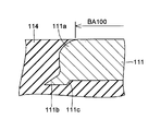
- the frame package type light emitting device is manufactured by using the conventional manufacturing method described above, as shown in FIG. A burr 111b is produced by punching at the outer edge of the other surface. Accordingly, the step 111c is formed in the vicinity of the outer edge on the other surface side of the frame 111 due to the influence of the burr 111b generated on the outer edge on the other surface side of the frame 111. That is, the other surface side of the frame 111 (the side where the burr 111b is formed on the outer edge) is a surface with unevenness, and is not a flat surface.
- one surface side of the frame 111 that is a substantially flat surface (the side where the sag 111a is formed on the outer edge) is used as a reference surface, and a light emitting element or a bonding wire is attached to the one surface side of the frame 111. Bonding.
- the molten resin is formed on one side of the frame 111 (the sag 111a on the outer edge).
- the outer edge region on one side of the frame 111 is covered with the resin molding portion 114. Therefore, there arises a disadvantage that the bonding area (area where die bonding or wire bonding can be performed) BA100 becomes narrow. In this case, if the size of the frame package type light emitting device is to be reduced, the bonding area BA100 is further reduced, which makes it difficult to reduce the size of the frame package type light emitting device.
- the other surface side of the frame 111 (the side where the burr 111b is formed on the outer edge) is used as a reference surface, and a light emitting element or a bonding wire is bonded to the other surface side of the frame 111. It is possible. However, since the other surface side of the frame 111 (the side where the burr 111b is formed on the outer edge) is not a flat surface, it is difficult to use it as a reference surface.
- the present invention has been made to solve the above-described problems, and an object of the present invention is to provide a frame package type light emitting device that can be miniaturized and a method for manufacturing the same.
- the light emitting element and the light emitting element are electrically connected, and a burr is generated at the outer edge on one side.
- a metal frame having a sag at the outer edge on the other surface side opposite to the one surface side, and a resin molded portion covering a part of the frame are provided.
- a conductive layer that fills the step formed by the generation of burrs is provided on one side of the frame, a light emitting element is mounted on one side of the frame, and electrically connected via a bonding wire. It is connected.
- the one side of the frame is the entire area ( (Including the outer edge region where burrs are generated) and a substantially flat surface.
- the outer edge region (the region where burrs are generated) on one side of the frame is also bonded. It can be used as an area. Therefore, even if the frame package type light emitting device is reduced in size, a sufficiently wide bonding area can be secured. As a result, it is possible to easily obtain a downsized frame package type light emitting device. In addition, since the bonding area is widened, the effect of facilitating the bonding work can be obtained.
- the conductive layer is selectively embedded in the concave portion of the step. If comprised in this way, the one surface side of a flame
- burrs extend in a direction orthogonal to the plate thickness direction of the frame. If comprised in this way, the area of the substantially flat surface of the one surface side of a flame
- the wraparound of the resin molded portion to one side of the frame is blocked by burrs. If comprised in this way, the inconvenience resulting from a resin molding part going around to the one surface side of a frame (the inconvenience that a bonding area will become narrow because the outer edge area
- a metal plate is prepared, and by punching the metal plate, a burr is generated on the outer edge on one side, and A step of producing a metal frame having a sag at the outer edge on the other side opposite to the direction side, a step of covering a part of the frame with a resin molding part, and electrically connecting the light emitting element to the frame Process. Then, prior to the step of covering a part of the frame with the resin molding portion, the conductive layer that fills the step formed by burrs is formed on one side of the frame by plating one side of the frame. A step of providing the light emitting element on one side of the frame, and electrically connecting via a bonding wire.
- the frame package type light emitting device by manufacturing the frame package type light emitting device using the manufacturing method as described above, there is no unevenness on one side of the frame, and one side of the frame is the entire area (burrs are generated.
- the surface is substantially flat over the outer edge region (including the outer edge region).
- the outer edge region on the one side of the frame can also be used as a bonding area. Therefore, even if the frame package type light emitting device is reduced in size, a sufficiently wide bonding area can be secured. As a result, it is possible to easily obtain a downsized frame package type light emitting device.
- the bonding area is widened, the effect of facilitating the bonding work can be obtained.
- the frame package type light emitting device can be easily downsized.
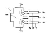
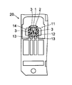
- FIG. 1 is a plan view of a frame package type light emitting device according to an embodiment of the present invention. It is a top view of the flame
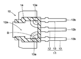
- FIG. 2 is a plan view for explaining the shape of a resin molded portion of the frame package type light emitting device shown in FIG. 1 (a view when viewed from the side where the light emitting element is mounted).
- FIG. 2 is a plan view for explaining the shape of a resin molded portion of the frame package type light emitting device shown in FIG.
- FIG. 1 (a view when viewed from the back side opposite to the side on which the light emitting element is mounted). It is sectional drawing of the area
- FIG. 10 is an enlarged plan view of a part of FIG. 9 (part which will later become a frame). It is sectional drawing of the area
- the frame package type light emitting device includes a semiconductor laser element 1, a frame package 10 on which the semiconductor laser element 1 is mounted, and the like. An electrical connection between the semiconductor laser element 1 and an external device (not shown) is performed via the frame package 10.
- the semiconductor laser element 1 is an example of the “light emitting element” in the present invention.
- the semiconductor laser device 1 is attached to the submount 2 by a junction down method, and is mounted on the frame package 10 in that state.
- the semiconductor laser element 1 is a two-wavelength laser element, and the p-side electrode is divided into two and the n-side electrode is common.
- the p-side electrode and the n-side electrode of the semiconductor laser element 1 are electrically connected to the frame package 10 through the bonding wires 3. Since the p-side electrode of the semiconductor laser element 1 is electrically connected to the electrode pad formed on the submount 2, the p-side electrode bonding wire 3 is bonded to the electrode pad of the submount 2. .
- the frame package 10 includes at least a frame 11 on which the semiconductor laser element 1 is mounted and electrically connected. As shown in FIGS. 1 and 2, the frame 11 includes one main frame portion 12 and two sub frame portions 13, which are electrically insulated from each other.
- the frame 11 is obtained by processing a metal plate (such as a copper plate or an iron plate) having a thickness of about 0.2 mm to about 0.5 mm, and is excellent in thermal conductivity and conductivity.
- the main frame portion 12 is a portion where the semiconductor laser element 1 is actually mounted and the n-side electrode of the semiconductor laser element 1 is electrically connected. That is, the main frame portion 12 has at least an element mounting portion 12a on which the semiconductor laser element 1 is mounted and an n-side electrode bonding wire 3 is bonded. And the lead
- the sub-frame portion 13 is a portion to which the p-side electrode (electrode pad of the submount 2) of the semiconductor laser element 1 is electrically connected, and the wire connection to which the p-side electrode bonding wire 3 is bonded. And a lead portion (portion connected to an external device) 13b extending integrally from the wire connection portion 13a. And this sub-frame part 13 is arrange
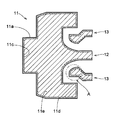
- the above-described frame 11 is formed by punching a metal plate. For this reason, as shown in FIGS. 3 and 4, a burr 11 a is formed on the outer edge of one side of the frame 11, and a sag 11 b is generated on the other side opposite to the one side of the frame 11. ing.
- the burr 11a is extended in the horizontal direction (direction orthogonal to the plate
- the frame 11 is subjected to a predetermined plating process (silver plating, palladium plating, gold plating, etc.) with a thickness of about 1 ⁇ m to about 3 ⁇ m over the entire surface. That is, the plating layer 11d having a thickness of about 1 ⁇ m to about 3 ⁇ m is formed on the entire surface of the frame 11.
- the plated layer 11d has a shape reflecting the unevenness caused by the presence of the step 11c.
- the burr 11a has a lateral protrusion L of about 30 ⁇ m, and the height difference (height in the plate thickness direction) H of the step 11c is about 5 ⁇ m. is there.
- the conductive layer 11e filling the step 11c is provided on one side of the frame 11. Specifically, by selectively embedding a conductive layer 11e having a thickness of about 5 ⁇ m in the concave portion of the step 11c, one side of the frame 11 is made a substantially flat surface. Therefore, a flat surface having a larger area on the burr surface side (one surface side of the frame 11 where the burr 11a is formed on the outer edge) than on the sag surface side (the other surface side of the frame 11 where the burr 11b is generated on the outer edge). It has become.
- the conductive layer 11e is a plated layer obtained by selectively plating one surface side of the frame 11 (silver plating, palladium plating, gold plating, etc.).
- the semiconductor laser element 1 (see FIG. 1) is mounted on one side of the frame 11 that has become a substantially flat surface by plating, and via the bonding wire 3 (see FIG. 1). Electrically connected.
- the surface on one side of the frame 11 is used as a reference surface (a surface serving as a reference when the frame 11 is applied to a jig or the like).
- the main frame portion 12 and the sub frame 13 are partially covered with a resin molding portion 14 and are fixed to each other by the resin molding portion 14.
- the resin molded portion 14 has a shape as shown in FIG. 5 in a plan view from the side on which the semiconductor laser element 1 is mounted (element mounting side). That is, the part on the element mounting side of the resin molded portion 14 surrounds the element mounting area and the area including the peripheral area from three directions in plan view, and the light emitting side of the semiconductor laser element 1 (see FIG. 1) is It is an open, substantially U-shape.
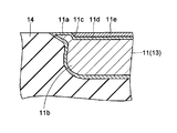
- the resin molded portion 14 is viewed from the side opposite to the element mounting side, the shape is as shown in FIG. In the present embodiment, as shown in FIG. 7, the wrapping of the resin molded portion 14 toward the one surface side of the frame 11 is blocked by the burr 11a.
- the conductive layer 11e is provided on one side of the frame 11, and the step 11c is filled with the conductive layer 11e.
- One surface side is a substantially flat surface over the entire region (including the outer edge region where the burr 11a is generated).
- the bonding area BA1 for bonding the bonding wire 3 is wider than the conventional bonding area BA100.
- the bonding area for bonding the semiconductor laser element 1 is also wider than the conventional one.
- the frame package type light emitting device is reduced in size, a sufficiently wide bonding area can be secured. As a result, it is possible to easily obtain a downsized frame package type light emitting device.
- the bonding area is widened, the effect of facilitating the bonding work can be obtained. Even if the length of the semiconductor laser element 1 in the resonator direction is increased, the bonding area is wide, so that the change can be easily handled.
- the conductive layer 11e for planarization is selectively embedded in the concave portion of the step 11c, so that one surface side of the frame 11 is easily substantially flat over the entire area. It can be a good surface.
- the area of the substantially flat surface on the one surface side of the frame 11 is further increased by the protrusion of the burr 11a in the horizontal direction.
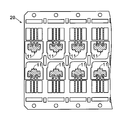
- a metal plate (not shown) is prepared, and the prepared metal plate is punched by a press, whereby FIG. 9 and FIG. A metal structure (which will later become the frame 11) 20 as shown in FIG. That is, a metal structure 20 is produced in which a plurality of frames 11 (the hatched portions in FIGS. 9 and 10) each including the main frame portion 12 and the sub-frame portion 13 are integrally connected.
- a burr 11a is generated at the outer edge on the one surface side of the frame 11, and a sag is formed on the outer edge on the other surface side of the frame 11.
- 11b is produced.
- a step 11 c is formed in the vicinity of the outer edge on the one surface side of the frame 11 due to the influence of the burr 11 a generated on the outer edge on the one surface side of the frame 11. The reason why the tip of the burr 11a is oriented in the direction (lateral direction) orthogonal to the plate thickness direction of the frame 11 is that the burr 11a is crushed by a press from the plate thickness direction of the frame 11.
- a predetermined plating process is performed on the entire surface of the frame 11 to form a plating layer 11 d on the entire surface of the frame 11.
- the step 11c remains without being filled. That is, one side of the frame 11 is not a flat surface.
- the step 11c is filled with the conductive layer 11e.
- the plating mask 21 is disposed so that only the concave portion of the step 11c is exposed, and in this state, a predetermined plating process is performed on one side of the frame 11.
- the conductive layer (plating layer) 11e is selectively embedded in the concave portion of the step 11c, and the one surface side of the frame 11 becomes a substantially flat surface.
- the plating mask 21 is removed.
- the burr 11a prevents the molten resin (which becomes the resin molded portion 14 from being cured) from wrapping around one side of the frame 11. Thereby, it can suppress that the outer edge area
- the semiconductor laser element 1 is mounted on the one surface side of the frame 11 while being attached to the submount 2. Then, the semiconductor laser element 1 is electrically connected to the frame 11 via the bonding wire 3. As a result, a plurality of frame package type light emitting devices are integrally connected. Finally, the frame package type light emitting device shown in FIG. 1 is manufactured by dividing it into individual pieces by pressing or dicing and cutting the connecting portion between the main frame portion 12 and the sub frame portion 13. Is done.
Landscapes
- Physics & Mathematics (AREA)
- Condensed Matter Physics & Semiconductors (AREA)
- General Physics & Mathematics (AREA)
- Electromagnetism (AREA)
- Optics & Photonics (AREA)
- Led Device Packages (AREA)
Abstract
【課題】小型化を図ることが可能なフレームパッケージ型発光装置を提供する。 【解決手段】このフレームパッケージ型発光装置は、半導体レーザ素子1と、その半導体レーザ素子1が電気的に接続されるとともに、一方面側の外縁にバリ11aが生じ、他方面側の外縁にダレ11bが生じているフレーム11とを備えている。そして、バリ11aが生じることで形成される段差11cを埋める導電層11eがフレーム11の一方面側に設けられており、そのフレーム11の一方面側に半導体レーザ素子1が搭載され、かつ、ボンディングワイヤ3を介して電気的に接続されている。
Description
本発明は、フレームパッケージ型発光装置およびその製造方法に関する。
従来、半導体レーザ素子などの発光素子をフレームパッケージと称されるものに搭載したフレームパッケージ型発光装置が知られている(たとえば、特許文献1参照)。
上記した従来のフレームパッケージ型発光装置のフレームパッケージは、一般的に、互いに電気的に絶縁された主フレーム部および副フレーム部からなる金属製のフレームを少なくとも備えており、その主フレーム部および副フレーム部が樹脂成形部によって互いに固着された構造となっている。なお、主フレーム部とは、発光素子が実際に搭載され、かつ、ボンディングワイヤを介して発光素子の一方電極と電気的に接続される部分である。また、副フレーム部とは、ボンディングワイヤを介して発光素子の他方電極と電気的に接続される部分である。
また、従来のフレームパッケージ型発光装置は、たとえば、以下のような工程を経て製造される。
すなわち、まず、金属板に対して打ち抜き加工を行うことにより、主フレーム部および副フレーム部からなるフレームが一体的に複数連結された金属構造体を作製する。次に、樹脂成形を行い、主フレーム部および副フレーム部が樹脂成形部によって互いに固着された状態にする。そして、主フレーム部に発光素子を搭載した後、ボンディングワイヤを介して、発光素子の一方電極を主フレーム部に電気的に接続するとともに、発光素子の他方電極を副フレーム部に電気的に接続する。これにより、複数のフレームパッケージ型発光装置が一体的に連結されたものが得られる。最後に、それを個片に分離することにより、従来のフレームパッケージ型発光装置が製造される。
ところで、上記した従来の製造方法を用いてフレームパッケージ型発光装置を製造した場合には、図17に示すように、フレーム111の一方面側の外縁に打ち抜き加工によるダレ111aが生じるとともに、フレーム111の他方面側の外縁に打ち抜き加工によるバリ111bが生じる。したがって、フレーム111の他方面側の外縁に生じたバリ111bの影響により、フレーム111の他方面側の外縁近傍には段差111cが形成された状態となる。すなわち、フレーム111の他方面側(外縁にバリ111bが生じている側)は凹凸が存在する面となり、平坦な面にはならない。このため、従来では、略平坦な面になっているフレーム111の一方面側(外縁にダレ111aが生じている側)を基準面とし、そのフレーム111の一方面側に発光素子やボンディングワイヤをボンディングしている。
しかしながら、上記した従来の構成では、樹脂成形工程(主フレーム部および副フレーム部を樹脂成形部114で互いに固着する工程)の際に、溶融樹脂がフレーム111の一方面側(外縁にダレ111aが生じている側)にまで回り込み、フレーム111の一方面側の外縁領域が樹脂成形部114で覆われた状態になってしまう。したがって、ボンディングエリア(ダイボンディングやワイヤボンディングが可能なエリア)BA100が狭くなるという不都合が生じる。この場合、フレームパッケージ型発光装置の小型化を図ろうとすると、ボンディングエリアBA100がさらに狭くなってしまうので、フレームパッケージ型発光装置を小型化するのが困難になるという問題点がある。
なお、上記した問題点を解消するために、フレーム111の他方面側(外縁にバリ111bが生じている側)を基準面とし、そのフレーム111の他方面側に発光素子やボンディングワイヤをボンディングすることが考えられる。しかしながら、フレーム111の他方面側(外縁にバリ111bが生じている側)は平坦な面ではないので、基準面としては利用し難い。
本発明は、上記した課題を解決するためになされたものであり、小型化を図ることが可能なフレームパッケージ型発光装置およびその製造方法を提供することを目的とする。
上記の目的を達成するために、本発明の第1の局面によるフレームパッケージ型発光装置は、発光素子と、発光素子が電気的に接続されるとともに、一方面側の外縁にバリが生じ、その一方面側とは反対の他方面側の外縁にダレが生じている金属製のフレームと、フレームの一部を覆う樹脂成形部とを備えている。そして、バリが生じることで形成される段差を埋める導電層がフレームの一方面側に設けられており、そのフレームの一方面側に発光素子が搭載され、かつ、ボンディングワイヤを介して電気的に接続されている。
第1の局面では、上記のように、フレームの一方面側に導電層を設け、その導電層で段差を埋めることによって、フレームの一方面側には凹凸がなくなり、フレームの一方面側が全域(バリが生じている外縁領域を含む)にわたって略平坦な面となる。この場合、フレームの一方面側に発光素子を搭載し、かつ、ボンディングワイヤを介して電気的に接続するようにすれば、フレームの一方面側の外縁領域(バリが生じている領域)もボンディングエリアとして活用することができる。したがって、フレームパッケージ型発光装置の小型化を図ったとしても、十分な広さのボンディングエリアを確保することができる。その結果、容易に、小型化されたフレームパッケージ型発光装置を得ることが可能となる。また、ボンディングエリアが広くなるので、ボンディング作業が容易になるという効果も得られる。
上記第1の局面によるフレームパッケージ型発光装置において、段差の凹側の部分に導電層が選択的に埋め込まれているのが好ましい。このように構成すれば、容易に、フレームの一方面側を全域にわたって略平坦な面にすることができる。
上記第1の局面によるフレームパッケージ型発光装置において、フレームの板厚方向と直交する方向にバリが延びているのが好ましい。このように構成すれば、フレームの板厚方向と直交する方向へのバリの突出分だけ、フレームの一方面側の略平坦となった面の面積をより広くすることができる。すなわち、ボンディングエリアをより広くすることができる。
上記第1の局面によるフレームパッケージ型発光装置において、フレームの一方面側への樹脂成形部の回り込みがバリによってせき止められた状態になっているのが好ましい。このように構成すれば、フレームの一方面側に樹脂成形部が回り込むことに起因する不都合(フレームの一方面側の外縁領域が樹脂成形部で覆われることによりボンディングエリアが狭くなってしまうという不都合)が発生するのを抑制することができる。
また、本発明の第2の局面によるフレームパッケージ型発光装置の製造方法は、金属板を準備し、その金属板に対して打ち抜き加工を行うことによって、一方面側の外縁にバリが生じ、一方面側とは反対の他方面側の外縁にダレが生じている金属製のフレームを作製する工程と、フレームの一部を樹脂成形部で覆う工程と、フレームに発光素子を電気的に接続する工程とを備えている。そして、フレームの一部を樹脂成形部で覆う工程に先立って、フレームの一方面側に対してメッキ処理を施すことによって、バリが生じることで形成される段差を埋める導電層をフレームの一方面側に設ける工程をさらに備え、そのフレームの一方面側に発光素子を搭載し、かつ、ボンディングワイヤを介して電気的に接続する。
この第2の局面では、上記のような製造方法を用いてフレームパッケージ型発光装置を製造することによって、フレームの一方面側には凹凸がなくなり、フレームの一方面側が全域(バリが生じている外縁領域を含む)にわたって略平坦な面となる。この場合、フレームの一方面側に発光素子を搭載し、かつ、ボンディングワイヤを介して電気的に接続するようにすれば、フレームの一方面側の外縁領域もボンディングエリアとして活用することができる。したがって、フレームパッケージ型発光装置の小型化を図ったとしても、十分な広さのボンディングエリアを確保することができる。その結果、容易に、小型化されたフレームパッケージ型発光装置を得ることが可能となる。また、ボンディングエリアが広くなるので、ボンディング作業が容易になるという効果も得られる。
以上のように、本発明によれば、容易に、フレームパッケージ型発光装置の小型化を図ることができる。
以下に、図1~図7を参照して、本実施形態によるフレームパッケージ型発光装置の構成について説明する。
本実施形態によるフレームパッケージ型発光装置は、図1に示すように、半導体レーザ素子1や、その半導体レーザ素子1が搭載されるフレームパッケージ10などによって構成されている。そして、半導体レーザ素子1と外部機器(図示せず)との間の電気的な接続がフレームパッケージ10を介して行われるようになっている。なお、半導体レーザ素子1は、本発明の「発光素子」の一例である。
この半導体レーザ素子1は、ジャンクションダウン方式でサブマウント2に取り付けられており、その状態でフレームパッケージ10に搭載されている。また、半導体レーザ素子1は2波長レーザ素子であって、p側電極が2つに分割され、n側電極が共通となっている。そして、半導体レーザ素子1のp側電極およびn側電極は、ボンディングワイヤ3を介してフレームパッケージ10に電気的に接続されている。なお、半導体レーザ素子1のp側電極はサブマウント2に形成された電極パッドに電気的に接続されているため、p側電極用のボンディングワイヤ3はサブマウント2の電極パッドにボンディングされている。
また、フレームパッケージ10は、半導体レーザ素子1が搭載され、かつ、電気的に接続されるフレーム11を少なくとも備えている。このフレーム11は、図1および図2に示すように、1つの主フレーム部12と2つの副フレーム部13とを含んでおり、それらが互いに電気的に絶縁された構造となっている。また、フレーム11は、約0.2mm~約0.5mmの厚みを有する金属板(銅板や鉄板など)を加工したものであって、熱伝導性および導電性に優れている。
主フレーム部12は、半導体レーザ素子1が実際に搭載されるとともに、半導体レーザ素子1のn側電極が電気的に接続される部分である。すなわち、主フレーム部12は、半導体レーザ素子1が搭載され、かつ、n側電極用のボンディングワイヤ3がボンディングされる素子搭載部12aを少なくとも有している。そして、その素子搭載部12aから一体的に延びるように、外部機器に接続されるリード部12bが設けられている。
また、副フレーム部13は、半導体レーザ素子1のp側電極(サブマウント2の電極パッド)が電気的に接続される部分であって、p側電極用のボンディングワイヤ3がボンディングされるワイヤ接続部13aと、そのワイヤ接続部13aから一体的に延びるリード部(外部機器に接続される部分)13bとを有している。そして、この副フレーム部13は、主フレーム部12のリード部12bを挟むように配置されている。
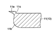
ところで、上記したフレーム11は、打ち抜き加工を金属板に対して行うことによって形成されたものである。このため、図3および図4に示すように、フレーム11の一方面側の外縁にはバリ11aが生じているとともに、フレーム11の一方面側とは反対の他方面側にはダレ11bが生じている。なお、バリ11aは、金属板に対する打ち抜き加工の後に押し潰されることによって、横方向(フレーム11の板厚方向と直交する方向)に延ばされている。また、このようなバリ11aがフレーム11の一方面側の外縁に生じているため、フレーム11の一方面側の外縁近傍には段差11cが形成された状態となっている。
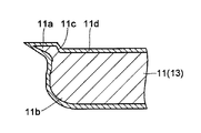
また、フレーム11は、その全面にわたって、所定のメッキ処理(銀メッキ、パラジウムメッキおよび金メッキなど)が約1μm~約3μmの厚みで施されている。すなわち、フレーム11の全面上に、約1μm~約3μmの厚みを有するメッキ層11dが形成されていることになる。なお、このメッキ層11dは、段差11cの存在によって生じる凹凸を反映した形状となっている。そして、フレーム11に対してメッキ処理が施された状態において、バリ11aの横方向への突出量Lは約30μmであり、段差11cの高低差(板厚方向の高さ)Hは約5μmである。
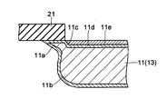
ここで、本実施形態では、段差11cを埋める導電層11eがフレーム11の一方面側に設けられている。具体的に言うと、約5μmの厚みを有する導電層11eを段差11cの凹側の部分に選択的に埋め込むことによって、フレーム11の一方面側を略平坦な面としている。このため、バリ面側(外縁にバリ11aが生じているフレーム11の一方面側)がダレ面側(外縁にダレ11bが生じているフレーム11の他方面側)よりも広い面積を持つ平坦面となっている。なお、導電層11eは、フレーム11の一方面側に対して選択的にメッキ処理(銀メッキ、パラジウムメッキおよび金メッキなど)を施すことによって得られるメッキ層である。
そして、本実施形態では、メッキ処理によって略平坦な面となったフレーム11の一方面側に半導体レーザ素子1(図1参照)が搭載され、かつ、ボンディングワイヤ3(図1参照)を介して電気的に接続されている。なお、本実施形態では、そのフレーム11の一方面側の面を基準面(フレーム11を治具などに当て付けて作業する場合に基準となる面)としている。
また、図1に示すように、主フレーム部12および副フレーム13は、それぞれの一部が樹脂成形部14で覆われており、その樹脂成形部14によって互いに固着されている。この樹脂成形部14は、半導体レーザ素子1が搭載される側(素子搭載側)からの平面視において、図5に示すような形状となっている。すなわち、樹脂成形部14の素子搭載側の部分は、平面的に見て、素子搭載領域およびその周辺領域を包含する領域を3方向から囲み、半導体レーザ素子1(図1参照)の光出射側が開放された略コの字形状となっている。一方、樹脂成形部14を素子搭載側とは反対側から見ると、図6に示すような形状となっている。そして、本実施形態では、図7に示すように、フレーム11の一方面側への樹脂成形部14の回り込みがバリ11aによってせき止められた状態となっている。
本実施形態では、上記のように、フレーム11の一方面側に導電層11eを設け、その導電層11eで段差11cを埋めることによって、フレーム11の一方面側には凹凸がなくなり、フレーム11の一方面側が全域(バリ11aが生じている外縁領域を含む)にわたって略平坦な面となる。この場合、フレーム11の一方面側に半導体レーザ素子1を搭載し、かつ、ボンディングワイヤ3を介して電気的に接続するようにすれば、フレーム11の一方面側の外縁領域(バリ11aが生じている領域)もボンディングエリアとして活用することができるので、図8に示すように、ボンディングワイヤ3をボンディングするためのボンディングエリアBA1が従来のボンディングエリアBA100に比べて広くなる。なお、図示しないが、半導体レーザ素子1をボンディングするためのボンディングエリアについても、従来のものに比べて広くなる。したがって、フレームパッケージ型発光装置の小型化を図ったとしても、十分な広さのボンディングエリアを確保することができ
る。その結果、容易に、小型化されたフレームパッケージ型発光装置を得ることが可能となる。また、ボンディングエリアが広くなるので、ボンディング作業が容易になるという効果も得られる。また、半導体レーザ素子1の共振器方向の長さをより大きくしたとしても、ボンディングエリアが広いので、その変更への対応が容易になる。
る。その結果、容易に、小型化されたフレームパッケージ型発光装置を得ることが可能となる。また、ボンディングエリアが広くなるので、ボンディング作業が容易になるという効果も得られる。また、半導体レーザ素子1の共振器方向の長さをより大きくしたとしても、ボンディングエリアが広いので、その変更への対応が容易になる。
また、本実施形態では、上記のように、平坦化のための導電層11eを段差11cの凹側の部分に選択的に埋め込むことによって、容易に、フレーム11の一方面側を全域にわたって略平坦な面にすることができる。
また、本実施形態では、上記のように、バリ11aを横方向に延ばすことによって、横方向へのバリ11aの突出分だけ、フレーム11の一方面側の略平坦となった面の面積をさらに広くすることができる。すなわち、ボンディングエリアをさらに広くすることができる。
以下に、図9~図16を参照して、本実施形態によるフレームパッケージ型発光装置の製造方法について説明する。
本実施形態のフレームパッケージ型発光装置の製造方法としては、まず、金属板(図示せず)を準備し、その準備した金属板に対してプレスによる打ち抜き加工を行うことによって、図9および図10に示すような金属構造体(後にフレーム11となるもの)20を作製する。すなわち、主フレーム部12および副フレーム部13をそれぞれ含む複数のフレーム11(図9および図10のハッチングが施された部分)が一体的に連結された金属構造体20を作製する。
なお、金属板に対して打ち抜き加工を行うことでフレーム11を作製すると、図11に示すように、フレーム11の一方面側の外縁にバリ11aが生じ、フレーム11の他方面側の外縁にダレ11bが生じる。また、フレーム11の一方面側の外縁に生じたバリ11aの影響により、フレーム11の一方面側の外縁近傍には段差11cが形成される。ところで、バリ11aの先端がフレーム11の板厚方向と直交する方向(横方向)に向いているのは、フレーム11の板厚方向からバリ11aをプレスで押し潰したためである。
次に、図12に示すように、フレーム11の全面に対して所定のメッキ処理を施すことによって、フレーム11の全面上にメッキ層11dを形成する。なお、この1回目のメッキ処理では、段差11cは埋められずに残存する。すなわち、フレーム11の一方面側は平坦な面にはなっていない。
続いて、本実施形態では、図13に示すように、フレーム11の一方面側に導電層11eを設けることによって、その導電層11eで段差11cを埋める。具体的には、段差11cの凹側の部分のみが露出するようにメッキマスク21を配置し、その状態で、フレーム11の一方面側に対して所定のメッキ処理を施す。これにより、導電層(メッキ層)11eが段差11cの凹側の部分に選択的に埋め込まれ、フレーム11の一方面側が略平坦な面となる。この後、メッキマスク21を取り外す。
次に、インサート成形を行うことによって、図14および図15に示すように、主フレーム部12および副フレーム部13を樹脂成形部14で互いに固着する。なお、この工程の際には、フレーム11の一方面側への溶融樹脂(硬化することで樹脂成形部14となるもの)の回り込みがバリ11a(図13参照)によってせき止められる。これにより、フレーム11の一方面側の外縁領域が樹脂成形部14で覆われた状態になるのを抑制することができる。
この後、図16に示すように、フレーム11の一方面側に、半導体レーザ素子1をサブマウント2に取り付けられた状態で搭載する。そして、ボンディングワイヤ3を介して、半導体レーザ素子1をフレーム11に電気的に接続する。これにより、複数のフレームパッケージ型発光装置が一体的に連結されたものが得られる。最後に、それをプレスやダイシングなどにより個片に分割するとともに、主フレーム部12と副フレーム部13との間の連結部分を切断することによって、図1に示したフレームパッケージ型発光装置が製造される。
今回開示された実施形態は、すべての点で例示であって制限的なものではないと考えられるべきである。本発明の範囲は、上記した実施形態の説明ではなく特許請求の範囲によって示され、さらに、特許請求の範囲と均等の意味および範囲内でのすべての変更が含まれる。
1 半導体レーザ素子(発光素子)
3 ボンディングワイヤ
11 フレーム
11a バリ
11b ダレ
11c 段差
11e 導電層
14 樹脂成形部
3 ボンディングワイヤ
11 フレーム
11a バリ
11b ダレ
11c 段差
11e 導電層
14 樹脂成形部
Claims (5)
- 発光素子と、
前記発光素子が電気的に接続されるとともに、一方面側の外縁にバリが生じ、前記一方面側とは反対の他方面側の外縁にダレが生じている金属製のフレームと、
前記フレームの一部を覆う樹脂成形部とを備え、
前記バリが生じることで形成される段差を埋める導電層が前記フレームの一方面側に設けられており、
前記フレームの一方面側に前記発光素子が搭載され、かつ、ボンディングワイヤを介して電気的に接続されていることを特徴とするフレームパッケージ型発光装置。 - 前記段差の凹側の部分に前記導電層が選択的に埋め込まれていることを特徴とする請求項1に記載のフレームパッケージ型発光装置。
- 前記フレームの板厚方向と直交する方向に前記バリが延びていることを特徴とする請求項1または2に記載のフレームパッケージ型発光装置。
- 前記フレームの一方面側への前記樹脂成形部の回り込みが前記バリによってせき止められた状態になっていることを特徴とする請求項1~3のいずれかに記載のフレームパッケージ型発光装置。
- 金属板を準備し、前記金属板に対して打ち抜き加工を行うことによって、一方面側の外縁にバリが生じ、前記一方面側とは反対の他方面側の外縁にダレが生じている金属製のフレームを作製する工程と、
前記フレームの一部を樹脂成形部で覆う工程と、
前記フレームに発光素子を電気的に接続する工程とを備え、
前記フレームの一部を前記樹脂成形部で覆う工程に先立って、前記フレームの一方面側に対してメッキ処理を施すことによって、前記バリが生じることで形成される段差を埋める導電層を前記フレームの一方面側に設ける工程をさらに備え、
前記フレームの一方面側に前記発光素子を搭載し、かつ、ボンディングワイヤを介して電気的に接続することを特徴とするフレームパッケージ型発光装置の製造方法。
Applications Claiming Priority (2)
| Application Number | Priority Date | Filing Date | Title |
|---|---|---|---|
| JP2009-042421 | 2009-02-25 | ||
| JP2009042421 | 2009-02-25 |
Publications (1)
| Publication Number | Publication Date |
|---|---|
| WO2010098156A1 true WO2010098156A1 (ja) | 2010-09-02 |
Family
ID=42665366
Family Applications (1)
| Application Number | Title | Priority Date | Filing Date |
|---|---|---|---|
| PCT/JP2010/050497 Ceased WO2010098156A1 (ja) | 2009-02-25 | 2010-01-18 | フレームパッケージ型発光装置およびその製造方法 |
Country Status (1)
| Country | Link |
|---|---|
| WO (1) | WO2010098156A1 (ja) |
Citations (5)
| Publication number | Priority date | Publication date | Assignee | Title |
|---|---|---|---|---|
| JPH01128456A (ja) * | 1987-11-12 | 1989-05-22 | Hitachi Ltd | 面実装型半導体デバイスおよびリードフレーム |
| JPH01129846U (ja) * | 1988-02-25 | 1989-09-04 | ||
| JPH03116770A (ja) * | 1989-09-28 | 1991-05-17 | Nec Kyushu Ltd | 半導体装置用リードフレーム |
| JP2002043679A (ja) * | 2000-07-28 | 2002-02-08 | Sanyo Electric Co Ltd | 半導体レーザ装置 |
| JP2002223003A (ja) * | 2001-01-26 | 2002-08-09 | Nichia Chem Ind Ltd | パッケージ成形体とその製造方法及び発光装置 |
-
2010
- 2010-01-18 WO PCT/JP2010/050497 patent/WO2010098156A1/ja not_active Ceased
Patent Citations (5)
| Publication number | Priority date | Publication date | Assignee | Title |
|---|---|---|---|---|
| JPH01128456A (ja) * | 1987-11-12 | 1989-05-22 | Hitachi Ltd | 面実装型半導体デバイスおよびリードフレーム |
| JPH01129846U (ja) * | 1988-02-25 | 1989-09-04 | ||
| JPH03116770A (ja) * | 1989-09-28 | 1991-05-17 | Nec Kyushu Ltd | 半導体装置用リードフレーム |
| JP2002043679A (ja) * | 2000-07-28 | 2002-02-08 | Sanyo Electric Co Ltd | 半導体レーザ装置 |
| JP2002223003A (ja) * | 2001-01-26 | 2002-08-09 | Nichia Chem Ind Ltd | パッケージ成形体とその製造方法及び発光装置 |
Similar Documents
| Publication | Publication Date | Title |
|---|---|---|
| US10985093B2 (en) | Semiconductor device and method for producing semiconductor device | |
| US7514293B2 (en) | Method of manufacturing a semiconductor device | |
| US8853841B2 (en) | Lead frame which includes terminal portion having through groove covered by lid portion, semiconductor package, and manufacturing method of the same | |
| JP2014183142A (ja) | 半導体装置、半導体装置の製造方法 | |
| JP6357371B2 (ja) | リードフレーム、半導体装置及びリードフレームの製造方法 | |
| JP2010080914A (ja) | 樹脂封止型半導体装置とその製造方法、リードフレーム | |
| JP5598189B2 (ja) | 半導体装置の製造方法 | |
| JP4804497B2 (ja) | 半導体装置 | |
| JP2017037898A (ja) | リードフレーム、半導体装置及びリードフレームの製造方法 | |
| JP2019121698A (ja) | 半導体装置および半導体装置の製造方法 | |
| US10026677B2 (en) | Semiconductor device | |
| US20230005827A1 (en) | Lead frame, semiconductor device, and lead frame manufacturing method | |
| JP2008501242A (ja) | 可撓性リードフレーム構造および集積回路パッケージの形成方法 | |
| JP2017152496A (ja) | リードフレーム、及び半導体パッケージの製造方法 | |
| JP5104020B2 (ja) | モールドパッケージ | |
| JP2015153987A (ja) | モールドパッケージ | |
| JP5180495B2 (ja) | 半導体装置およびその製造方法 | |
| JP2016032076A (ja) | 電子デバイスの製造方法及び電子デバイス | |
| JP2015029143A (ja) | 樹脂封止型半導体装置とその製造方法、リードフレーム | |
| KR20200001803U (ko) | 예비성형 리드 프레임 및 그것으로 제조된 리드 프레임 패키지 | |
| JP2013235896A (ja) | 半導体装置の製造方法及び半導体装置 | |
| JP2010056339A (ja) | 半導体装置の製造方法 | |
| JP2010278046A (ja) | モールドパッケージの製造方法及びモールドパッケージ | |
| JP2005057099A (ja) | 半導体装置およびその製造方法 | |
| JP2019186338A (ja) | 半導体装置 |
Legal Events
| Date | Code | Title | Description |
|---|---|---|---|
| 121 | Ep: the epo has been informed by wipo that ep was designated in this application |
Ref document number: 10746038 Country of ref document: EP Kind code of ref document: A1 |
|
| NENP | Non-entry into the national phase |
Ref country code: DE |
|
| 122 | Ep: pct application non-entry in european phase |
Ref document number: 10746038 Country of ref document: EP Kind code of ref document: A1 |
|
| NENP | Non-entry into the national phase |
Ref country code: JP |