WO2010095657A1 - 放射線検出モジュール及び放射線撮像装置 - Google Patents
放射線検出モジュール及び放射線撮像装置 Download PDFInfo
- Publication number
- WO2010095657A1 WO2010095657A1 PCT/JP2010/052363 JP2010052363W WO2010095657A1 WO 2010095657 A1 WO2010095657 A1 WO 2010095657A1 JP 2010052363 W JP2010052363 W JP 2010052363W WO 2010095657 A1 WO2010095657 A1 WO 2010095657A1
- Authority
- WO
- WIPO (PCT)
- Prior art keywords
- radiation
- radiation detection
- support substrate
- detection module
- pixels
- Prior art date
- Legal status (The legal status is an assumption and is not a legal conclusion. Google has not performed a legal analysis and makes no representation as to the accuracy of the status listed.)
- Ceased
Links
Images

Classifications
-
- H—ELECTRICITY
- H10—SEMICONDUCTOR DEVICES; ELECTRIC SOLID-STATE DEVICES NOT OTHERWISE PROVIDED FOR
- H10F—INORGANIC SEMICONDUCTOR DEVICES SENSITIVE TO INFRARED RADIATION, LIGHT, ELECTROMAGNETIC RADIATION OF SHORTER WAVELENGTH OR CORPUSCULAR RADIATION
- H10F39/00—Integrated devices, or assemblies of multiple devices, comprising at least one element covered by group H10F30/00, e.g. radiation detectors comprising photodiode arrays
- H10F39/10—Integrated devices
- H10F39/12—Image sensors
- H10F39/18—Complementary metal-oxide-semiconductor [CMOS] image sensors; Photodiode array image sensors
- H10F39/189—X-ray, gamma-ray or corpuscular radiation imagers
Definitions
- the present invention relates to a radiation detection module and a radiation imaging apparatus, and more particularly to a technology capable of obtaining an image of high quality and facilitating assembly.
- one readout circuit is provided for one pixel element, and detection signals which are output upon incidence of radiation are individually read out to specify the incident position of the radiation.
- the upper limit of the integration degree of the readout circuit limits the increase in area of the radiation incident surface and the increase in pixel density.
- a double-sided silicon strip detector (DSSD) has been devised as a method of reading a large number of pixels with a small number of readout circuits.
- DSSD double-sided silicon strip detector
- a plurality of elongated electrodes are provided orthogonal to the upper and lower surfaces of the detector, and the incident position of the radiation is specified by reading out signals from both sides.
- N ⁇ M pixels by N + M readout circuits is established (see, for example, Non-Patent Document 1).
- the unit group of pixels needs to have a shape close to a square in order to obtain the reduction effect of the readout circuit. For this reason, when one of the unit clusters of the pixels breaks down, radiation can not be detected in the square area. In this case, it is difficult to complement data from surrounding pixel data, and a hole is formed in the image. Furthermore, in the technique of Non-Patent Document 1, it is necessary to increase the thickness of the detector in order to prevent penetration of the radiation and improve the detection efficiency, since the radiation is perpendicularly incident on the electrode surface of the detector. . However, when the thickness of the detector is increased, the mobility of the charge generated in the detector is reduced and the charge collection efficiency is reduced, so that the technique of Non-Patent Document 1 can not accurately measure the generated charge amount.
- Patent Document 1 discloses a technique in which radiation is incident in parallel to the electrode surface of a detection element in order to make two contradictory conditions regarding the thickness of the detector compatible. Further, in the technology of Patent Document 1, the signal wires drawn from the electrodes are connected on a separately provided substrate to reduce the number of read circuits using the same principle as that of the DSSD.
- An object of the present invention is to solve such problems, and to provide a radiation detection module that improves the image quality of an image and facilitates mounting and assembly of a radiation detection element, and a radiation imaging apparatus. Do.
- a plurality of first electrodes provided corresponding to one pixel are provided on one side of the semiconductor member, and a plurality of first electrodes are provided on the other side of the semiconductor member.
- a radiation detection element which outputs a detection signal to the first electrode and the second electrode when radiation is incident, and is erected along the incident direction of the radiation; Is detachably connected to a support substrate supporting a plurality of radiation detection elements arranged in orthogonal directions, and an external connection portion, and a bias voltage to the radiation detection elements is supplied from the connection portion, and a detection signal is transmitted to the connection portion And a connection portion for mechanically holding the support substrate against the connection portion, A plurality of first electrodes are connected on the support substrate, and the incident position of the radiation in the module is specified by simultaneously measuring detection signals from the first electrode and the second electrode.
- the number of signal lines drawn to the outside can be reduced, and the structure of the external connection portion and the connection portion for holding the support substrate in the connection portion can be simplified, and adjacent The intervals of the radiation detection modules can be narrowed.
- m radiation detection elements each having n pixels it is possible to reduce the number of reading wirings of detection signals to m + n while providing m ⁇ n pixels in one radiation detection module.
- the resistor and the capacitor are conventionally disposed on the outer side where the coupling portion is provided, the degree of integration of the wiring on the outer side is alleviated by moving to a vacant space of the support substrate.
- the portion where the high voltage is applied to the signal contact portion between the wires in the connection portion and the connection portion is reduced. Also, by making the unit group of pixels rectangular, it is possible to complement data from surrounding pixel data even if one of the pixels fails.
- a radiation detection module and a radiation imaging apparatus are provided that improve the image quality of the image and facilitate the mounting and maintenance of the detection element.
- FIG. 1 is an overall view showing a radiation imaging apparatus according to an embodiment of the present invention.
- FIG. 2 is an internal structural view of the radiation imaging apparatus according to the embodiment of the present invention.
- FIG. 3A is a perspective view of a radiation detection module according to an embodiment of the present invention, and
- FIG. 3B is a radiation detection element applied to the radiation detection module.
- Fig.4 (a) is a top view of the radiation detection module which concerns on embodiment, (b) is a side view, (c) is a top view which concerns on a modification, (d) is a deformation
- FIG. 5 is a circuit diagram of the radiation detection module according to the embodiment.
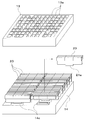
- the radiation imaging apparatus 10 includes an imaging unit 15 in which a collimator 13 disposed to be a radiation incident surface is fixed to a frame 15 a, and data from the imaging unit 15 as a cable 12. And an image display unit 11 for collecting and displaying an image.
- the main configuration of the radiation imaging apparatus 10 described with reference to the later drawings is accommodated.
- a radioactive substance that generates gamma rays (radiation) having an energy of several tens of keV to several hundreds of keV is used for an imaging object of a gamma camera (radiographic imaging apparatus 10). Then, measurement is performed for each event of one radiation incident on the imaging unit 15, and an image obtained by the integration is displayed on the image display unit 11.
- the collimator 13 is made of a material having a high radiation shielding ability, such as lead, and provided with a large number of elongated hole openings 13a so that only radiation incident from a specific direction (the Z-axis direction in the drawing) passes.
- a radiation source not shown
- a planar image of the luminance distribution of the radiation is formed on the imaging unit 15.
- the luminance distribution of the radiation formed as a planar image is processed by the radiation detection module 20 (see FIG. 2) and the signal detection unit 14 inside the imaging unit 15, and information such as the radiation detection position and radiation detection energy It is sent to the image display unit 11 after being converted into digital data.
- the image display unit 11 creates an image using correction data and the like collected in advance based on the detected position and energy of the sent digital data, and displays the image on the screen.
- SPECT Single Photon Emission Computer Tomography
- the imaging unit 15 is rotated or arranged in multiple places around the subject who has administered the radioactive drug. Three-dimensional cross-sectional image information can be obtained.
- FIG. 2 shows the structure internally contained in the frame 15a (see FIG. 1).
- the internal structure is planarly arranged such that a plurality of radiation detection modules 20 for detecting incident radiation are parallel to the inside of the collimator 13.
- the plurality of radiation detection modules 20 can be detachably attached to the connection portion 14 c provided on the surface of the signal detection unit 14 at the connection portion 21 a.
- connection portion 21a mechanically holding the radiation detection module 20 in the external connection portion 14c
- the radiation detection module via the connection portion 14c is supplied with a bias voltage supplied from the signal detection portion 14 side. 20, and the detection signal that the radiation detection module 20 detects and outputs radiation is led to the signal detection unit 14 side via the connection unit 14c.
- the connection portion 21a obtains electrical conduction by mechanically contacting the contact point (not shown) of the connection portion 14c on the surface of the contact point 22 (see FIG. 3A).
- the connection portion 21a is not limited to one formed on the extension surface of the support substrate 21 as illustrated, and a pin insertion type or a bellows type connector may be employed.
- the signal detection unit 14 amplifies and detects an analog minute electric signal (detection signal) led from the radiation detection module 20 that has detected the radiation. Furthermore, the signal detection unit 14 includes a high voltage generation circuit, and supplies a high voltage bias voltage to the radiation detection module 20.
- a circuit that amplifies and detects a detection signal is an application specific integrated circuit (ASIC) custom designed and manufactured based on the specification of the system. Then, this ASIC measures the peak value of the amplified detection signal. Next, time information when the detection signal is detected and address information of the detection pixel Pn (see FIG. 4A) which added the detection signal are added to the peak value to form a digital signal. Then, this digital signal is sent to the image display unit 11 via the cable 12 (see FIG. 1).
- the address information of the detection pixel Pn is represented by binary information as described later.
- the radiation detection module 20 includes a support substrate 21 having a connecting portion 21a formed at an edge and a plurality of radiation detection elements 30 mounted on the support substrate 21.
- a support substrate 21 having a connecting portion 21a formed at an edge and a plurality of radiation detection elements 30 mounted on the support substrate 21.
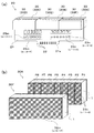
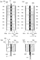
- a plurality of radiation detection elements 30 are arrayed in the direction perpendicular to the incident direction (the reference numerals 30A to 30C in the figure) on the surface of the support substrate 21 standing along the incident direction of the radiation (Z axis in FIG. 1). Of 30D to 30F on the other side, three on each side (total six). Then, as shown in FIG. 3B, the semiconductor member 1 constituting one radiation detection element 30 is provided with a plurality of detection pixels Pn (eight pieces of reference symbols P1 to P8 in the figure). .
- the radiation detection element 30 is made of a semiconductor member 1 such as CdTe or CZT, and the first electrode 31n and the second electrode 32m disposed on both sides thereof are formed by depositing Pt or In on the crystal surface by sputtering or the like. is there. Further, a method of forming the divided first electrode 31n is performed by using a mask at the time of vapor deposition or by vapor-depositing the entire surface, and then cutting out the electrode surface by dicing.
- the thing comprised with the semiconductor member 1 which the some detection pixel Pn integrated was illustrated as a radiation detection element 30, it is not limited to this, It isolate
- the ones having the same n number are connected to the common wiring (see FIG. 5 as needed).
- the first electrodes 31 n facing each other across the support substrate 21 can be electrically connected by forming through holes in the support substrate 21 and filling the conductors 33 n.
- two first opposing electrically conductive plates 34n are provided so as to sandwich electrically conductive plate 34n standing from the peripheral edge of support substrate 21 respectively.
- the electrodes 31 n and 31 n may be disposed.
- resistors 23n and 25m and the capacitors 24n and 26m as signal processing elements mounted on the support substrate 21 are only examples, and any other components mounted inside the signal detection unit 14 (see FIG. 2). Can be transferred onto this support substrate 21. Specifically, it is also conceivable to mount on the supporting substrate 21 the aforementioned ASIC or the like that converts a weak analog signal (detection signal) output from an electrode into a digital signal.
- the high voltage bias resistor 25 m prevents the signal applied from the electrode from flowing to the bias power supply. (See also Figure 5 as appropriate).
- the low-voltage coupling capacitor 24n is also connected to all (six) of the first electrodes 31n corresponding to n numbers among the radiation detection elements 30 (30A to 30F) on the support substrate 21 on one side, and the other side is a signal It is connected to the ASIC circuit of the detection unit 14 (see FIG. 2).
- the low voltage DC component (DC component) of the detection signal output from the first electrode 31 n is cut, and only the signal component based on the charge generation described later generated inside the radiation detection element 30 is an ASIC circuit.
- the low voltage bias resistor 23 n and the low voltage coupling capacitor 24 n may be formed as a special circuit in an ASIC without being mounted on the support substrate 21.
- the radiation detection element 30 may be arrange
- the number of reading wirings of the detection signal can be m + n in the number of pixels of m ⁇ n (in addition, a ground wiring and a bias voltage wiring are required).
- a negative bias voltage is applied to the second electrode 32m is illustrated (see FIG. 4B), a positive bias voltage may be applied.
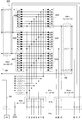
- the circuit of the radiation detection module 20 will be described with reference to FIG.
- the wiring from the second electrode 32m (see FIG. 4) disposed in all the radiation detection elements 30 (30A to 30F) is connected to the high voltage bias wiring 28 via the corresponding high voltage bias resistance 25m (25A to 25F) It is done.
- a high voltage of about -500 V is applied to the high voltage bias interconnection 28.
- the high voltage bias voltage is appropriately set in accordance with the direction and thickness of the diode characteristic of the radiation detection element 30.
- high voltage coupling capacitors 26m (26A to 26F) are connected to the wiring from the respective second electrodes 32m, and the bias voltage (DC voltage component) applied to the second electrodes 32m is cut. , Only the detection signal output from the radiation detection element 30 is allowed to pass. The detection signal with the bias voltage cut off is taken out of the radiation detection module 20 through the connection 21 a. As described above, by cutting the high DC voltage component inside the radiation detection module 20, the portion to which the high voltage is applied to the contact 22 of the connection portion 21a (FIG. 3A) is reduced, and the reliability is improved. .
- connection part 21a and the connection part 14c are relatively simple.
- this signal detection unit it is determined that radiation has entered the first detection pixel P1 in the radiation detection element 30A by simultaneously detecting the detection signals in the first wiring and the A wiring.
- an orthogonal signal readout circuit similar to the conventional DSSD in a pseudo manner, and specify the incident position of the radiation by simultaneous determination of detection signals. It is characterized by
- the detection pixels Pn are arranged in the order of 1 to 8 in all the radiation detection elements 30, but detection is possible if the individual radiation detection elements 30 do not have the numbers 1 to 8 in duplicate.
- the radiation detection elements 30A, 30C, 30D, and 30F may be arranged in the order of 1 to 8, and the radiation detection elements 30B and 30E may be arranged in the order of 8 to 1, respectively.
- the plurality of radiation detection elements 30 are arranged in a long direction in one direction, thereby reducing the influence of failure of the one radiation detection module 20. Can. That is, the missing image portion obtained when one radiation detection module 20 fails can be complemented using the image data of the adjacent normal radiation detection module 20.
- the radiation irradiation surface usually has a certain extent of spread, so a plurality of radiation detection modules 20 having an elongated shape detect the radiation irradiation surface of the radiation Will share. As a result, detection signals output from the radiation detection module 20 are dispersed, dead time is reduced, and data reliability is improved.
- signal processing elements such as capacitors and resistors can be disposed on the support substrate 21, only a part of the contacts 22 in the connection portion 21 a and the connection portion 14 c, that is, only the high voltage bias wiring 28 is high. It is only necessary to supply a voltage, which simplifies the isolation structure. Furthermore, since the degree of integration of the wiring with respect to the detection pixel Pn can be reduced, the detection pixel Pn can be made higher in density, so that the image quality can be improved.
- SYMBOLS 1 semiconductor member 10 radiation imaging device 11 image display part 14 signal detection part 14c connection part 15 imaging part 20 radiation detection module 21 support substrate 21a connection part 22 contact point 23n low voltage
Landscapes
- Measurement Of Radiation (AREA)
- Light Receiving Elements (AREA)
- Apparatus For Radiation Diagnosis (AREA)
Priority Applications (1)
| Application Number | Priority Date | Filing Date | Title |
|---|---|---|---|
| US13/201,914 US20110297837A1 (en) | 2009-02-17 | 2010-02-17 | Radiation detection module and radiation image-capturing device |
Applications Claiming Priority (2)
| Application Number | Priority Date | Filing Date | Title |
|---|---|---|---|
| JP2009034147A JP5027832B2 (ja) | 2009-02-17 | 2009-02-17 | 放射線検出モジュール及び放射線撮像装置 |
| JP2009-034147 | 2009-02-17 |
Publications (1)
| Publication Number | Publication Date |
|---|---|
| WO2010095657A1 true WO2010095657A1 (ja) | 2010-08-26 |
Family
ID=42633937
Family Applications (1)
| Application Number | Title | Priority Date | Filing Date |
|---|---|---|---|
| PCT/JP2010/052363 Ceased WO2010095657A1 (ja) | 2009-02-17 | 2010-02-17 | 放射線検出モジュール及び放射線撮像装置 |
Country Status (3)
| Country | Link |
|---|---|
| US (1) | US20110297837A1 (enExample) |
| JP (1) | JP5027832B2 (enExample) |
| WO (1) | WO2010095657A1 (enExample) |
Cited By (1)
| Publication number | Priority date | Publication date | Assignee | Title |
|---|---|---|---|---|
| US9698181B2 (en) | 2011-08-03 | 2017-07-04 | Oxford University Innovation Limited | Semiconductor detector device |
Families Citing this family (5)
| Publication number | Priority date | Publication date | Assignee | Title |
|---|---|---|---|---|
| JP2012103036A (ja) * | 2010-11-08 | 2012-05-31 | Hitachi Consumer Electronics Co Ltd | 放射線検出器 |
| CN102592938B (zh) * | 2012-01-06 | 2016-03-30 | 同方威视技术股份有限公司 | 离子迁移管信号提取电路、方法以及离子迁移探测器 |
| DE102014222690B4 (de) | 2014-11-06 | 2024-10-02 | Siemens Healthineers Ag | Detektormodul für einen Röntgendetektor |
| JP6591908B2 (ja) * | 2016-02-18 | 2019-10-16 | 国立大学法人 東京大学 | 放射線検出装置 |
| CN108419026B (zh) * | 2018-05-31 | 2020-05-15 | 歌尔股份有限公司 | 相机曝光时间调整方法、装置及设备 |
Citations (5)
| Publication number | Priority date | Publication date | Assignee | Title |
|---|---|---|---|---|
| JP2008004949A (ja) * | 2007-07-17 | 2008-01-10 | Hitachi Ltd | 半導体放射線検出器及び半導体放射線撮像装置 |
| JP2008107326A (ja) * | 2006-09-29 | 2008-05-08 | Hitachi Ltd | 核医学診断装置 |
| JP2008161689A (ja) * | 2007-01-04 | 2008-07-17 | General Electric Co <Ge> | 計算機式断層写真法検出器モジュール構成 |
| JP2008171881A (ja) * | 2007-01-09 | 2008-07-24 | Shimadzu Corp | 光または放射線検出器 |
| JP2008286560A (ja) * | 2007-05-15 | 2008-11-27 | Hitachi Ltd | 結晶素子組み立て体、そのための電気回路、それらを用いた核医学診断装置及び通電制御方法 |
Family Cites Families (7)
| Publication number | Priority date | Publication date | Assignee | Title |
|---|---|---|---|---|
| JPH0816702B2 (ja) * | 1983-12-26 | 1996-02-21 | 株式会社島津製作所 | 半導体放射線位置検出装置 |
| US6621084B1 (en) * | 1998-09-24 | 2003-09-16 | Elgems Ltd. | Pixelated photon detector |
| IL143980A0 (en) * | 2001-06-25 | 2002-04-21 | Imarad Imaging Systems Ltd | Three dimensional radiation detection |
| JP2005109269A (ja) * | 2003-09-30 | 2005-04-21 | Hitachi Ltd | 半導体放射線検出器及び半導体放射線撮像装置 |
| US7212604B2 (en) * | 2005-06-29 | 2007-05-01 | General Electric Company | Multi-layer direct conversion computed tomography detector module |
| JP3858044B1 (ja) * | 2005-09-09 | 2006-12-13 | 株式会社日立製作所 | 放射線検出モジュール、プリント基板および陽電子放出型断層撮影装置 |
| US7525098B2 (en) * | 2006-04-05 | 2009-04-28 | Orbotech Ltd. | High resolution energy detector |
-
2009
- 2009-02-17 JP JP2009034147A patent/JP5027832B2/ja not_active Expired - Fee Related
-
2010
- 2010-02-17 WO PCT/JP2010/052363 patent/WO2010095657A1/ja not_active Ceased
- 2010-02-17 US US13/201,914 patent/US20110297837A1/en not_active Abandoned
Patent Citations (5)
| Publication number | Priority date | Publication date | Assignee | Title |
|---|---|---|---|---|
| JP2008107326A (ja) * | 2006-09-29 | 2008-05-08 | Hitachi Ltd | 核医学診断装置 |
| JP2008161689A (ja) * | 2007-01-04 | 2008-07-17 | General Electric Co <Ge> | 計算機式断層写真法検出器モジュール構成 |
| JP2008171881A (ja) * | 2007-01-09 | 2008-07-24 | Shimadzu Corp | 光または放射線検出器 |
| JP2008286560A (ja) * | 2007-05-15 | 2008-11-27 | Hitachi Ltd | 結晶素子組み立て体、そのための電気回路、それらを用いた核医学診断装置及び通電制御方法 |
| JP2008004949A (ja) * | 2007-07-17 | 2008-01-10 | Hitachi Ltd | 半導体放射線検出器及び半導体放射線撮像装置 |
Cited By (1)
| Publication number | Priority date | Publication date | Assignee | Title |
|---|---|---|---|---|
| US9698181B2 (en) | 2011-08-03 | 2017-07-04 | Oxford University Innovation Limited | Semiconductor detector device |
Also Published As
| Publication number | Publication date |
|---|---|
| US20110297837A1 (en) | 2011-12-08 |
| JP5027832B2 (ja) | 2012-09-19 |
| JP2010190665A (ja) | 2010-09-02 |
Similar Documents
| Publication | Publication Date | Title |
|---|---|---|
| US9306108B2 (en) | Radiation detector | |
| JP3858044B1 (ja) | 放射線検出モジュール、プリント基板および陽電子放出型断層撮影装置 | |
| US20070278414A1 (en) | Semiconductor radiological detector and semiconductor radiological imaging apparatus | |
| US7247860B2 (en) | Radiation detection module, radiation detector and radiological imaging apparatus | |
| JP5027832B2 (ja) | 放射線検出モジュール及び放射線撮像装置 | |
| JP6721682B2 (ja) | 放射線検出器及び撮像装置 | |
| CN101326449A (zh) | 放射线检测单元以及放射线检查装置 | |
| US20100308230A1 (en) | Detector array substrate and nuclear medicine diagnosis device using same | |
| US7645998B2 (en) | Detector module, detector and computed tomography unit | |
| JP2005201642A (ja) | 放射線検出装置および核医学診断装置 | |
| CN104414676A (zh) | X射线探测器和方法 | |
| US20140348290A1 (en) | Apparatus and Method for Low Capacitance Packaging for Direct Conversion X-Ray or Gamma Ray Detector | |
| JP2005106692A (ja) | 半導体放射線検出器及び放射線撮像装置 | |
| JP4934826B2 (ja) | 放射線画像検出モジュールおよび放射線画像検出装置 | |
| JP4464998B2 (ja) | 半導体検出器モジュール、および該半導体検出器モジュールを用いた放射線検出装置または核医学診断装置 | |
| JP2008191165A (ja) | 検出器モジュール及び放射線撮像装置 | |
| JP5070637B2 (ja) | 放射線画像検出モジュール | |
| JP5136736B2 (ja) | 放射線画像検出モジュールおよび放射線画像検出装置 | |
| JP2021535590A (ja) | イメージセンサ、イメージセンサ装置、及び、これらを含むコンピュータ断層撮影装置 | |
| JP5044809B2 (ja) | 放射線検出器及び放射線撮像装置 | |
| US8748840B2 (en) | High-resolution compact gamma burst detector | |
| CN114868041A (zh) | 光子计数探测器 | |
| JP2015125063A (ja) | 放射線検出器 | |
| TW569030B (en) | Radiation image detector | |
| TW202305406A (zh) | 使用成像系統的電池卷測試方法 |
Legal Events
| Date | Code | Title | Description |
|---|---|---|---|
| 121 | Ep: the epo has been informed by wipo that ep was designated in this application |
Ref document number: 10743783 Country of ref document: EP Kind code of ref document: A1 |
|
| NENP | Non-entry into the national phase |
Ref country code: DE |
|
| WWE | Wipo information: entry into national phase |
Ref document number: 13201914 Country of ref document: US |
|
| 122 | Ep: pct application non-entry in european phase |
Ref document number: 10743783 Country of ref document: EP Kind code of ref document: A1 |