WO2010092722A1 - 光学素子及びその製造方法 - Google Patents
光学素子及びその製造方法 Download PDFInfo
- Publication number
- WO2010092722A1 WO2010092722A1 PCT/JP2009/069610 JP2009069610W WO2010092722A1 WO 2010092722 A1 WO2010092722 A1 WO 2010092722A1 JP 2009069610 W JP2009069610 W JP 2009069610W WO 2010092722 A1 WO2010092722 A1 WO 2010092722A1
- Authority
- WO
- WIPO (PCT)
- Prior art keywords
- optical element
- sample
- antireflection film
- molded part
- optical
- Prior art date
- Legal status (The legal status is an assumption and is not a legal conclusion. Google has not performed a legal analysis and makes no representation as to the accuracy of the status listed.)
- Ceased
Links
Images
Classifications
-
- G—PHYSICS
- G02—OPTICS
- G02B—OPTICAL ELEMENTS, SYSTEMS OR APPARATUS
- G02B1/00—Optical elements characterised by the material of which they are made; Optical coatings for optical elements
- G02B1/10—Optical coatings produced by application to, or surface treatment of, optical elements
- G02B1/11—Anti-reflection coatings
- G02B1/113—Anti-reflection coatings using inorganic layer materials only
-
- G—PHYSICS
- G02—OPTICS
- G02B—OPTICAL ELEMENTS, SYSTEMS OR APPARATUS
- G02B1/00—Optical elements characterised by the material of which they are made; Optical coatings for optical elements
- G02B1/04—Optical elements characterised by the material of which they are made; Optical coatings for optical elements made of organic materials, e.g. plastics
- G02B1/041—Lenses
-
- G—PHYSICS
- G11—INFORMATION STORAGE
- G11B—INFORMATION STORAGE BASED ON RELATIVE MOVEMENT BETWEEN RECORD CARRIER AND TRANSDUCER
- G11B7/00—Recording or reproducing by optical means, e.g. recording using a thermal beam of optical radiation by modifying optical properties or the physical structure, reproducing using an optical beam at lower power by sensing optical properties; Record carriers therefor
- G11B7/12—Heads, e.g. forming of the optical beam spot or modulation of the optical beam
- G11B7/135—Means for guiding the beam from the source to the record carrier or from the record carrier to the detector
- G11B7/1372—Lenses
- G11B7/1374—Objective lenses
Definitions
- the present invention relates to an optical element and a manufacturing method thereof.
- plastic optical elements that can be mass-produced at low cost have been used as optical systems used for reading and writing optical information recording media such as CDs and DVDs.
- plastic material cycloolefin resins having excellent characteristics such as low moisture absorption, high transmittance, and low birefringence are frequently used.
- an antireflection film composed of an inorganic oxide is usually formed on the optical surface of an optical element, and a technique such as vacuum deposition is widely used as a film forming technique. It has been.
- the resin portion of the optical element is organic, the antireflection film is inorganic, and the linear expansion coefficient is different from each other. In addition, sufficient adhesiveness cannot be obtained, so the phenomenon of film peeling occurs. What happens is a problem. In addition, when the film strength is not sufficient, deformation due to deterioration of the resin surface that occurs when the antireflection film is irradiated with laser light cannot be suppressed, resulting in deformation of the resin and spherical aberration of the optical element. It became clear that there may be fluctuations.
- a main object of the present invention is to provide an optical element that suppresses film peeling of an antireflection film and suppresses deformation of a resin, and thereby has less variation in spherical aberration, and a method for manufacturing the same.
- XPS X-ray photoelectron spectroscopy
- a precursor of an inorganic compound layer containing carbon atoms is formed according to a sol-gel method, and the precursor is sintered while irradiating the precursor with infrared rays,
- a method for producing an optical element characterized in that the inorganic compound layer having a carbon concentration detected by X-ray photoelectron spectroscopy (XPS) of 0.2 to 5 atomic% is formed.
- XPS X-ray photoelectron spectroscopy
- the present invention since a certain range of carbon atoms is contained in the layer of the antireflection film, it is possible to suppress deformation of the resin molded part while suppressing film peeling of the antireflection film. In addition, it is possible to provide an optical element in which the antireflection film does not peel off and the variation of spherical aberration is small.
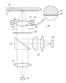
- the optical pickup device 30 is provided with a semiconductor laser oscillator 32.
- the semiconductor laser oscillator 32 is an example of a light source, and emits blue laser light (blue-violet laser) with a specific wavelength (for example, 405 nm) having a wavelength of 350 to 450 nm for BD (Blu-ray Disc).
- a collimator 33, a beam splitter 34, a quarter wavelength plate 35, a diaphragm 36, and an objective lens 37 are arranged in a direction away from the semiconductor laser oscillator 32. Are sequentially arranged.
- a sensor lens group 38 and a sensor 39 made up of two sets of lenses are sequentially arranged in a direction close to the beam splitter 34 and perpendicular to the optical axis of the blue-violet light described above.
- the objective lens 37 is disposed at a position facing the high-density optical disc D (BD optical disc), and condenses the blue laser light emitted from the semiconductor laser oscillator 32 on one surface of the optical disc D. Yes.
- the objective lens 37 is an example of an optical element, and the image-side numerical aperture NA is 0.7 or more.
- a flange portion is formed on the periphery of the objective lens 37, and a two-dimensional actuator 40 is mounted on the flange portion. By the operation of the two-dimensional actuator 40, the objective lens 37 is movable on the optical axis.
- the objective lens 37 is mainly composed of a molding portion 50, and an antireflection film 55 is formed on each of the front surface 37a and the rear surface 37b (the front surface 37a in FIG. 1). Only the antireflection film 55 is depicted.)
- the molding part 50 is molded into a lens shape, and the front surface 37a and the back surface 37b are optical surfaces so as to exhibit essential optical functions such as a light collecting function.
- Molding part 50 is made of cycloolefin resin.
- An example of a cycloolefin resin that can form the molded part 50 is disclosed in Japanese Patent Application Laid-Open No. 2005-221988 (see paragraphs 0014 to 0148). Specifically, Nippon Zeon: ZEONEX, Mitsui Chemicals: APEL, JSR: Arton, Chicona: TOPAS, etc. are suitably used as the cycloolefin resin.
- the antireflection film which is an inorganic compound layer and has a specific carbon concentration is an antireflection film formed on the optical surface of the molded part.
- the antireflection film formed on the optical surface of the molding part is an antireflection film formed in contact with the molding part.
- the antireflection film 55 may have a single layer structure or a multiple layer structure. That is, another antireflection layer may be provided on the antireflection layer according to the present invention.
- the antireflection film 55 exhibits a sufficient antireflection function even if it has a single layer structure, but a multi-layer structure composed of two or more layers can enhance the antireflection effect.
- the antireflection film 55 is an inorganic compound layer (a layer composed of an inorganic compound), and the inorganic compound layer includes Si, Al, Zr, Ti, Ta, Ce, Hf, La, and Ge. It preferably contains at least one element.
- the layer can be composed of SiO 2 , Al 2 O 3 , ZrO 2 or the like.
- the antireflection film may have a 2 to 7 layer structure as a whole.
- the layer that is in direct contact with the molded part 50 is an inorganic compound layer having a specific amount of carbon according to the present invention.
- the antireflection film according to the present invention is preferably a film containing Si, and particularly preferably a film containing Si.
- the antireflection film is made of SiO 2 .
- an antireflection film having a refractive index of 1.30 to 1.42 is preferably used, and an antireflection film containing Si and having a refractive index in this range is particularly preferable. The adjustment of the refractive index will be described later.
- the cycloolefin resin is injection-molded into a mold under a certain condition to form a molded part 50 having a predetermined shape.
- an antireflection film 55 is formed on each of the front surface 37a and the back surface 37b of the molded part 50.
- the processes (1) and (2) are performed according to the sol-gel method.
- the “sol-gel processing” here is a known sol-gel method, and generally a sol composed of a metal alkoxide is used as a gel that loses fluidity, and the gel is heated to obtain an oxide. Is the method.
- a certain compound is prepared to prepare a precursor (sol) of an inorganic compound layer, and the molding part 50 is immersed in the sol for a certain period of time and pulled out from the sol, and then the molding part 50 is dried.
- the sol applied to the front surface 37a and the back surface 37b is gelled.
- a metal alkoxide having an alkoxy group (and / or a condensate thereof) is preferably used.
- the metal alkoxide is represented by the formula (A).
- R 1 x M (OR 2 ) y (A)
- substituents represented by “R 1” represents an alkyl group
- R 2 represents a lower alkyl group
- M is a constituent metal and is not particularly limited, but silicon, aluminum, zirconium and titanium are preferable from the viewpoint of ease of use.
- the metal alkoxide represented by the formula (A) is a bifunctional, trifunctional, or tetrafunctional metal alkoxide.
- bifunctional metal alkoxide examples include dimethyldimethoxysilane, dimethyldiethoxysilane, dialkoxyzirconium and dialkoxytitanium corresponding to these.
- trifunctional metal alkoxide examples include methyltrimethoxysilane, methyltriethoxysilane, phenyltrimethoxysilane, phenyltriethoxysilane, corresponding trialkoxyaluminum (including tripropoxyaluminum), trialkoxyzirconium, trialkoxy Examples include titanium.
- tetrafunctional metal alkoxides include tetramethoxysilane, tetraethoxysilane, tetra-n-propoxysilane, tetraisopropoxysilane, tetra-n-butoxysilane, tetraisobutoxysilane, tetra-sec-butoxysilane, and tetra-tert.
- the metal alkoxide can be used alone or in combination of two or more.
- the mixing ratio in the case of using two or more kinds of metal alkoxides is arbitrary, but as the blending ratio of the tetrafunctional metal alkoxide increases, the reactivity increases and a hard coating film can be obtained.
- the metal alkoxide may be a condensate.
- Examples of commercial products available as metal alkoxide condensates include M-silicate 51, M-silicate 56, M-silicate 60, silicate 40, silicate 45, and silicate 48 manufactured by Tama Chemical Co., Ltd.
- the surface 37a and the back surface 37b of the molded part 50 are heated and sintered while being irradiated with infrared rays intermittently.
- an infrared heater manufactured by Elstin can be used, and preferably a ceramic bar type heater (HLS series) manufactured by Elstin can be used.
- a shielding plate having a light shielding property is arranged between them, and the shielding plate is periodically inserted and removed (opening and closing). Or periodically switching ON / OFF of the infrared irradiation device itself.
- the inorganic compound layer whose carbon concentration detected by X-ray photoelectron spectroscopy (XPS) is 0.2 to 5 atomic% is formed on the front surface 37a and the back surface 37b of the molded part 50.
- the objective lens 37 can be manufactured.
- the heating / sintering time of (2) may be increased or the amount of infrared irradiation light may be increased, and the carbon concentration in the antireflection film 55 is adjusted by adjusting as appropriate. be able to.
- the refractive index of the inorganic compound layer according to the present invention is preferably 1.30 to 1.42, but in order to make the refractive index within this range, the above (1), (2
- the drying conditions (drying temperature and drying time) in the drying process may be adjusted.
- the antireflection film 55 having a desired refractive index can be obtained by changing the drying conditions in the drying step and drying the molded part 50 having the surface coated with the sol.
- the layer that contacts the molded part is formed according to the sol-gel method described above.
- the layer other than the layer may be formed by other methods (vacuum deposition, sputtering, etc.) (Of course, the layer other than the layer may be formed according to the sol-gel method described above).
- the antireflection film 55 is formed on the front surface 37a and the back surface 37b of the objective lens 37 is shown in the present embodiment, it may be formed on any one surface.
- Blue laser light is emitted from the semiconductor laser oscillator 32 during an operation of recording information on the optical disc D or an operation of reproducing information recorded on the optical disc D.
- the emitted blue laser light passes through the collimator 33 and is collimated into infinite parallel light, then passes through the beam splitter 34 and passes through the quarter wavelength plate 35. Furthermore, after passing through the blue laser beam aperture 36 and the objective lens 37, forms a converged spot on an information recording surface D 2 through the protective substrate D 1 of the optical disc D.
- Blue laser light that formed the concentrated light spot is modulated by the information recording surface D 2 of the optical disk D by the information bits, is reflected by the information recording surface D 2. Then, the reflected light is sequentially transmitted through the objective lens 37 and the diaphragm 36, and then the polarization direction is changed by the 1 / wavelength plate 35 and reflected by the beam splitter 34. Thereafter, the reflected light passes through the sensor lens group 38 to be given astigmatism, is received by the sensor 39, and finally is photoelectrically converted by the sensor 39 to become an electrical signal.
- the antireflection film 55 contains a certain range of carbon atoms having a carbon concentration of 0.2 to 5 atomic% in the layer of the antireflection film 55. It is possible to suppress deformation of the resin molding part 50 while suppressing film peeling, and to obtain an optical element with little variation in spherical aberration.
- Example 1 (1) Sample preparation (1.1) Sample 1 ZEONEX 340R manufactured by Nippon Zeon Co., Ltd. was used as the cycloolefin resin, and the resin was injection molded to produce an objective lens (molded part) of a Blu-ray optical system having an effective system diameter of 3 mm and a numerical aperture of 0.85.
- an inorganic compound precursor was prepared using a sol-gel method. Specifically, tetraethoxysilane / ethanol / water / hydrochloric acid were mixed at a molar ratio of 1/5/10 / 0.01 and stirred. The molded part was immersed in the obtained sol, and then the molded part was pulled up from the sol at a speed of 1 mm / min along the direction in which the flange part becomes vertical. The molded part was dried at 60 ° C. for 4 hours.
- thermocouple was arrange
- a ceramic shielding plate was installed between the heater and the molded portion, and the infrared irradiation time (intermittent infrared irradiation) on the molded portion was controlled by inserting and removing the shielding plate.
- irradiation heating to the S1 surface of the molded part with an infrared heater was performed for 0.2 seconds, and immediately after that, a 4-second pause (heat radiation) time was given by shielding with a ceramic plate.
- This infrared irradiation cycle was repeated 10 times.
- the same process was performed also on the S2 surface (light emitting surface) of the molded part (infrared irradiation method A).
- the optical element obtained here was designated as “Sample 1”.
- Sample 5 For the same objective lens as Sample 1, without using the sol-gel method and without infrared irradiation, as an alternative method, the silicon oxide layer is formed by vacuum deposition on both the S1 and S2 surfaces of the molded part. Was formed (vacuum deposition method), and this was designated as “Sample 5”.
- tripropoxyaluminum / isopropanol / water / hydrochloric acid was mixed and stirred at a molar ratio of 1/5/10 / 0.01.
- the molded part was immersed in the obtained sol, and then the molded part was pulled up from the sol at a speed of 1 mm / min along the direction in which the flange part becomes vertical.
- the molded part was dried at 60 ° C. for 4 hours.
- thermocouple was arrange
- an optical element was produced according to the infrared irradiation method A of Sample 1, and this was designated as “Sample 6”.
- Sample 10 For an objective lens similar to that of Sample 1, an aluminum oxide layer is formed by vacuum deposition (see Sample 5) as an alternative method without using the sol-gel method and without performing infrared irradiation, and this is referred to as “Sample 10”. "
- tetrapropoxyzirconium / isopropanol / water / hydrochloric acid were mixed at a molar ratio of 1/5/10 / 0.01 and stirred.
- the molded part was immersed in the obtained sol, and then the molded part was pulled up in the sol at a speed of 1 mm / min along the direction in which the flange part becomes vertical.
- the molded part was dried at 60 ° C. for 4 hours.
- thermocouple was arrange
- an optical element was produced according to the infrared irradiation method A of Sample 1, and this was designated as “Sample 11”.
- sample evaluation Measurement of film thickness In each sample 1-15, analysis was performed by spectral reflection spectrum. As a result, the thickness of each of samples 1-5 (silicon oxide layer) was about 70 nm. Samples 6 to 10 (aluminum oxide layer) had a thickness of about 75 nm, and samples 11 to 15 (zirconium oxide layer) had a thickness of about 70 nm.
- Example 2 ⁇ Preparation of optical element sample 1> (Production process of objective lens (molded part)) ZEONEX 340R manufactured by Nippon Zeon Co., Ltd. was used as the cycloolefin resin, and the resin was injection molded to produce an objective lens (molded part) of a Blu-ray optical system having an effective diameter of 3 mm and a numerical aperture of 0.85.
- the precursor of the silicon compound was produced using the sol-gel method. Specifically, tetraethoxysilane / ethanol / water / hydrochloric acid were mixed at a molar ratio of 1/5/10 / 0.01 and stirred. The objective lens (molded part) was immersed in the obtained sol, and then the objective lens was pulled up from the sol at a speed of 1 mm / min along the direction in which the flange part was vertical.
- the objective lens after drying was placed so that the S1 surface (light incident surface) faces the infrared heater, and the objective lens was placed at a predetermined position so that the temperature of the thermocouple was 500 ° C.
- the thermocouple was disposed in the vicinity of the objective lens, and was disposed at the same distance as the distance between the objective lens and the heater with respect to the heater.
- a ceramic shielding plate was installed between the heater and the objective lens, and the infrared irradiation time (intermittent infrared irradiation) on the objective lens was controlled by inserting and removing the shielding plate.
- irradiation heating to the S1 surface of the objective lens by an infrared heater was performed for 0.2 seconds, and immediately after that, a 4-second pause (heat radiation) time was given by shielding with a ceramic plate. This infrared irradiation cycle was repeated 5 times. Further, the same processing was performed on the S2 surface (light emitting surface) of the objective lens. Thus, an optical element sample 1 having a silicon oxide film (antireflection film 55) formed on the surface was produced.
- Optical element sample 2 was produced by carrying out in the same manner as production of optical element sample 1 except for the drying conditions in the drying step.
- Optical element sample 3 was produced by carrying out in the same manner as the production of optical element sample 1 except for the drying conditions in the drying step.
- the refractive index nd of the antireflection film according to the optical element sample 1 was 1.41
- the refractive index nd of the antireflection film according to the optical element sample 2 was 1.31
- the refractive index nd of the antireflection film according to the optical element sample 3 was 1.45.
- the antireflection film according to the optical element samples 1 to 3 of the present invention is an antireflection film produced by intermittent irradiation of infrared rays, has no film peeling, and has little deformation of the resin. I understand.
- the optical element samples 1 and 2 are preferable because the refractive index of the silicon oxide film (antireflection film) is included in the range of 1.30 to 1.42, and the transmittance is good (90% or more). It was a thing.
Landscapes
- Physics & Mathematics (AREA)
- Optics & Photonics (AREA)
- General Physics & Mathematics (AREA)
- Chemical & Material Sciences (AREA)
- Inorganic Chemistry (AREA)
- Optical Head (AREA)
- Surface Treatment Of Optical Elements (AREA)
Abstract
本発明は、光学素子であって、シクロオレフィン樹脂製の成形部と、前記成形部の光学面上に形成された反射防止膜とを、備え、前記反射防止膜が無機化合物層であり、前記無機化合物層のX線光電子分光法(XPS)により検出される炭素濃度が0.2~5atomic%であることを特徴とし、反射防止膜の膜剥れがなく、球面収差の変動が少ない光学素子が提供できる。
Description
本発明は光学素子及びその製造方法に関する。
従来から、CDやDVDなどの光情報記録媒体の読取りや書込みに使用される光学系として、安価に大量生産が可能なプラスチック製の光学素子が使用されている。そのプラスチック材料としては、低吸湿、高透過率、低複屈折などの特性に優れたシクロオレフィン系の樹脂が多用されている。
近年では、記録密度を高めたBlu-ray光学系が主流となってきている。当該光学系では、波長405nm付近のレーザが使用されるため、ピックアップレンズなどの光学素子に耐光性が必要とされ、例えば、特許文献1に記載の技術では、耐光性が改良されたシクロオレフィン樹脂の使用が試みられている。
さらに近年では、光学素子の光学面に対し無機酸化物から構成される反射防止膜が形成されるのが通常となっており、その製膜技術として、真空蒸着などの手法が広く一般的に用いられている。
しかしながら、光学素子の樹脂部分が有機物であるのに対し反射防止膜は無機物であり、その線膨張係数が互いに異なることに加え、十分な接着性が得られないために、膜剥れの現象が生じることが問題となっている。また、膜の強度が十分でない場合には、反射防止膜がレーザ光の照射を受けた際に発生する樹脂表面の劣化による変形を抑制できず、その結果樹脂が変形して光学素子の球面収差が変動したりする場合があることが明らかになった。
したがって、本発明の主な目的は、反射防止膜の膜剥れが抑えられ、樹脂の変形が抑制されることで球面収差の変動が少ない光学素子及びその製造方法を提供することにある。
そこで、本発明者がこのような問題に鑑みその解決策を検討したところ、無機酸化物からなる反射防止膜中に炭素原子を導入することで樹脂と反射防止膜との接着性を高め、膜剥がれを抑制できることが明らかになった。しかしながら、炭素原子の濃度が高すぎると反射防止膜の強度が十分に得られず、樹脂の変形を抑制できないことが明らかになった。
これらの課題は、下記の構成により解決できる。
本発明の一態様によれば、
シクロオレフィン樹脂製の成形部と、
前記成形部の光学面上に形成された反射防止膜とを、備え、
前記反射防止膜が無機化合物層であり、
前記無機化合物層のX線光電子分光法(XPS)により検出される炭素濃度が0.2~5atomic%であることを特徴とする光学素子が提供される。
シクロオレフィン樹脂製の成形部と、
前記成形部の光学面上に形成された反射防止膜とを、備え、
前記反射防止膜が無機化合物層であり、
前記無機化合物層のX線光電子分光法(XPS)により検出される炭素濃度が0.2~5atomic%であることを特徴とする光学素子が提供される。
本発明の他の態様によれば、
シクロオレフィン樹脂を成形して成形部を形成する工程と、
前記成形部上に反射防止膜を形成する工程とを、備え、
前記反射防止膜を形成する工程では、ゾルゲル法にしたがって、炭素原子を含む無機化合物層の前駆体を形成し、その前駆体に対し断続的に赤外線を照射しながら前記前駆体を焼結し、X線光電子分光法(XPS)により検出される炭素濃度が0.2~5atomic%である前記無機化合物層を形成することを特徴とする光学素子の製造方法が提供される。
シクロオレフィン樹脂を成形して成形部を形成する工程と、
前記成形部上に反射防止膜を形成する工程とを、備え、
前記反射防止膜を形成する工程では、ゾルゲル法にしたがって、炭素原子を含む無機化合物層の前駆体を形成し、その前駆体に対し断続的に赤外線を照射しながら前記前駆体を焼結し、X線光電子分光法(XPS)により検出される炭素濃度が0.2~5atomic%である前記無機化合物層を形成することを特徴とする光学素子の製造方法が提供される。
本発明によれば、反射防止膜の層中に、一定範囲の炭素原子が含有されるから、反射防止膜の膜剥れを抑えながらも、樹脂製の成形部の変形を抑制することができ、反射防止膜の膜剥れがなく、球面収差の変動が少ない光学素子が提供できる。
以下、図面を参照しながら本発明の好ましい実施形態について説明する。
図1に示す通り、光ピックアップ装置30には、半導体レーザ発振器32が具備されている。半導体レーザ発振器32は光源の一例であり、BD(Blu-ray Disc)用として波長350~450nmの特定波長(例えば405nm)のブルーレーザ光(青紫色レーザ)を出射するようになっている。半導体レーザ発振器32から出射されるブルーレーザ光の光軸上には、半導体レーザ発振器32から離間する方向に向かって、コリメータ33、ビームスプリッタ34、1/4波長板35、絞り36、対物レンズ37が順次配設されている。
ビームスプリッタ34と近接した位置であって、上述した青紫色光の光軸と直交する方向には、2組のレンズからなるセンサーレンズ群38、センサー39が順次配設されている。
対物レンズ37は、高密度な光ディスクD(BD用光ディスク)に対向した位置に配置されており、半導体レーザ発振器32から出射されたブルーレーザ光を光ディスクDの一面上に集光するようになっている。対物レンズ37は光学素子の一例であり、像側開口数NAが0.7以上となっている。対物レンズ37の周縁部にはフランジ部が形成されており、当該フランジ部に2次元アクチュエータ40が装着されている。2次元アクチュエータ40の動作により、対物レンズ37は光軸上を移動自在となっている。
図1中拡大図に示す通り、対物レンズ37は主には成形部50で構成されており、その表面37aと裏面37bとに対しそれぞれ反射防止膜55が形成されている(図1では表面37aに対してのみ反射防止膜55が描写されている。)。成形部50はレンズ形状に成形されており、表面37aと裏面37bとが光学面となって集光機能などの本質的な光学機能を発揮するようになっている。
成形部50はシクロオレフィン樹脂で構成されている。成形部50を構成可能なシクロオレフィン樹脂の一例が特開2005-221988号公報(段落0014~0148など参照)に開示されている。具体的には、シクロオレフィン樹脂として、日本ゼオン製:ZEONEX、三井化学製:APEL、JSR製:アートン、チコナ製:TOPASなどが好適に用いられる。
本発明において、無機化合物層であって、上記炭素濃度が特定のものである反射防止膜は、成形部の光学面上に形成された反射防止膜である。成形部の光学面上に形成された反射防止膜とは成形部に接触して形成された反射防止膜である。
反射防止膜55は単層構造を有してもよいし、複数層構造を有してもよい。即ち、本発明に係る反射防止層の上に他の反射防止層を有していてもよい。
反射防止膜55は単層構造であっても反射防止機能を十分に発揮するが、2層以上の層から構成される複数層構造のほうが反射防止効果を高めることができる。
本実施の形態では、反射防止膜55が無機化合物層(無機化合物から構成された層)であり、その無機化合物層はSi,Al,Zr,Ti,Ta,Ce,Hf,La,Geのうち少なくとも1つの元素を含有していることが好ましい。
反射防止膜55を単層構造とする場合、その層はSiO2,Al2O3,ZrO2などで構成することができる。
対物レンズ37では、例えば反射防止膜を全体で2~7層構造としてもよい。この場合、成形部50に直に接触する層は、本発明に係る特定量の炭素を有する無機化合物層である。
本発明に係る反射防止膜としては、Siを含有する膜が好ましく、特にSiを含有する膜であることが好ましい。この場合反射防止膜は、SiO2で構成される。
また、本発明に係る反射防止膜としては、屈折率が1.30~1.42である反射防止膜が好ましく用いられ、特にSiを含有し屈折率がこの範囲である反射防止膜が好ましい。屈折率の調整については後述する。
続いて、対物レンズ37の製造方法について説明する。
始めに、上記シクロオレフィン樹脂を一定条件下で金型に対し射出成形し、所定形状を有する成形部50を形成する。
その後、成形部50の表面37aと裏面37bとに対しそれぞれ反射防止膜55を形成する。この工程では、ゾルゲル法にしたがって、(1),(2)の処理を行う。ここでいう「ゾルゲル法(Sol-Gel processing)」とは、公知のゾルゲル法であって、一般に金属アルコキシドからなるゾルを、流動性を失ったゲルとし、このゲルを加熱して酸化物を得る方法である。
(1)はじめに、一定の化合物を調製して無機化合物層の前駆体(ゾル)を作製し、そのゾル中に成形部50を一定時間浸漬して当該ゾル中から引き上げ、その後成形部50を乾燥させ、表面37aと裏面37bとに塗布したゾルをゲル化する。
(1)はじめに、一定の化合物を調製して無機化合物層の前駆体(ゾル)を作製し、そのゾル中に成形部50を一定時間浸漬して当該ゾル中から引き上げ、その後成形部50を乾燥させ、表面37aと裏面37bとに塗布したゾルをゲル化する。
当該前駆体としては、好ましくはアルコキシ基を有する金属アルコキシド(及び/又はその縮合体)を使用する。
具体的に、金属アルコキシドは式(A)で表される。
(R1)xM(OR2)y … (A)
式(A)中、「R1」で示される置換基はアルキル基を表し、「R2」は低級アルキル基を表す。「x」及び「y」は、x+y=4でかつ「x」は2以下となる整数を表す。「M」は構成金属であって、特に制限はないが、使いやすさの観点から、珪素、アルミニウム、ジルコニウム、チタニウムが望ましい。
式(A)中、「R1」で示される置換基はアルキル基を表し、「R2」は低級アルキル基を表す。「x」及び「y」は、x+y=4でかつ「x」は2以下となる整数を表す。「M」は構成金属であって、特に制限はないが、使いやすさの観点から、珪素、アルミニウム、ジルコニウム、チタニウムが望ましい。
式(A)で示された金属アルコキシドは、2官能性、3官能性、4官能性の金属アルコキシドを示している。
2官能性金属アルコキシドとしては、ジメチルジメトキシシラン、ジメチルジエトキシシラン、これらに対応するジアルコキシジルコニウム、ジアルコキシチタンなどが挙げられる。
3官能性金属アルコキシドとしては、メチルトリメトキシシラン、メチルトリエトキシシラン、フェニルトリメトキシシラン、フェニルトリエトキシシラン、これらに対応するトリアルコキシアルミニウム(トリプロポキシアルミニウムを含む。)、トリアルコキシジルコニウム、トリアルコキシチタンなどが挙げられる。
4官能性金属アルコキシドとしては、テトラメトキシシラン、テトラエトキシシラン、テトラ-n-プロポキシシラン、テトライソプロポキシシラン、テトラ-n-ブトキシシラン、テトライソブトキシシラン、テトラ-sec-ブトキシシラン、テトラ-tert-ブトキシシラン、これらに対応するテトラアルコキシジルコニウム(テトラプロポキシジルコニウムを含む。)、テトラアルコキシチタンなどが挙げられる。
前記金属アルコキシドは、1種単独であるいは2種以上を組み合わせて使用することができる。
2種類以上の金属アルコキシドを使用する場合の混合比は任意であるが、4官能性の金属アルコキシドの配合比率が高くなるにつれて、反応性が増し、硬い塗膜を得ることができる。
一方、2官能または3官能性の金属アルコキシドの配合比率が高くなるにつれて、柔軟性の高い塗膜を得ることができる。
前記金属アルコキシドは縮合体を使用しても良い。
金属アルコキシドの縮合体として市販されている商品としては、多摩化学(株)製 Mシリケート51、Mシリケート56、Mシリケート60、シリケート40、シリケート45、シリケート48等を挙げることができる。
(2)次に、成形部50の表面37aと裏面37bとに形成した前駆体(ゲル)を一定温度で加熱して当該前駆体を焼結する。
(2)次に、成形部50の表面37aと裏面37bとに形成した前駆体(ゲル)を一定温度で加熱して当該前駆体を焼結する。
この場合、例えば、成形部50の表面37aと裏面37bとにそれぞれ対し断続的に赤外線を照射しながら加熱・焼結する。赤外線の照射装置としては、例えばエルスティン社製赤外線ヒータを用いることができ、好ましくはエルスティン社製セラミックバータイプヒータ(HLSシリーズ)を用いることができる。
赤外線を断続的に照射するときは、赤外線の照射装置と成形部50とを対向配置した状態で、その間に赤外線に遮光性を有する遮蔽板を配置し当該遮蔽板を定期的に抜き差し(開閉)したり、赤外線の照射装置自体のON/OFFを定期的に切り替えたりすればよい。
以上の(1),(2)の処理により、X線光電子分光法(XPS)により検出される炭素濃度が0.2~5atomic%である無機化合物層を、成形部50の表面37aと裏面37bとにそれぞれ形成することができ、その結果対物レンズ37を製造することができる。炭素濃度を減少させるためには、(2)の加熱・焼結時間を長くするか、赤外線の照射光量を増加させればよく、適宜調整することで反射防止膜55中の炭素濃度を調整することができる。
また、本発明に係る無機化合物層の屈折率は上記のように、1.30~1.42であることが好ましいが、屈折率をこの範囲とするためには、上記(1)、(2)に加えて、乾燥工程における乾燥条件(乾燥温度及び乾燥時間)を調整すれば良い。換言すると、乾燥工程における乾燥条件を変えて、表面にゾルが塗布された成形部50を乾燥させることで、所望の屈折率を有する反射防止膜55が得られる。また、赤外線を断続的に照射しながら加熱・焼結することにより、成形部50の溶融変形を避けることが可能となる。
なお、成形部50に対し複数層構造の反射防止膜55を形成する場合には、反射防止膜55を形成する層のうち、成形部に接触する層が上記したゾルゲル法にしたがって形成されればよく、その層以外は他の手法(真空蒸着やスパッタリングなど)により形成されてもよい(もちろんその層以外も上記したゾルゲル法にしたがって形成されてもよい。)。
さらに、本実施形態では対物レンズ37の表面37aと裏面37bとに反射防止膜55が形成された例を示したが、いずれか一方の面に形成されてもよい。
続いて、光ピックアップ装置30の動作について説明する。
光ディスクDへの情報の記録動作時や光ディスクDに記録された情報の再生動作時に、半導体レーザ発振器32からブルーレーザ光が出射される。出射されたブルーレーザ光は、コリメータ33を透過して無限平行光にコリメートされた後、ビームスプリッタ34を透過して、1/4波長板35を透過する。さらに、当該ブルーレーザ光は絞り36及び対物レンズ37を透過した後、光ディスクDの保護基板D1を介して情報記録面D2に集光スポットを形成する。
集光スポットを形成したブルーレーザ光は、光ディスクDの情報記録面D2で情報ビットによって変調され、情報記録面D2によって反射される。そして、この反射光は、対物レンズ37及び絞り36を順次透過した後、1/波長板35によって偏光方向が変更され、ビームスプリッタ34で反射する。その後、当該反射光は、センサーレンズ群38を透過して非点収差が与えられ、センサー39で受光されて、最終的には、センサー39によって光電変換されることによって電気的な信号となる。
以後、このような動作が繰り返し行われ、光ディスクDに対する情報の記録動作や、光ディスクDに記録された情報の再生動作が完了する。
以上の本実施形態によれば、対物レンズ37においては、反射防止膜55の層中に、炭素濃度が0.2~5atomic%である一定範囲の炭素原子が含有されるから、反射防止膜55の膜剥れを抑えながらも樹脂製の成形部50の変形を抑制することができ、球面収差の変動が少ない光学素子を得ることができる。
(実施例1)
(1)サンプルの作製
(1.1)サンプル1
シクロオレフィン樹脂として日本ゼオン社製ゼオネックス340Rを使用し、当該樹脂を射出成形して有効系φ3mm、開口数0.85のBlu-ray光学系の対物レンズ(成形部)を作製した。
(1)サンプルの作製
(1.1)サンプル1
シクロオレフィン樹脂として日本ゼオン社製ゼオネックス340Rを使用し、当該樹脂を射出成形して有効系φ3mm、開口数0.85のBlu-ray光学系の対物レンズ(成形部)を作製した。
その後、ゾルゲル法を用いて無機化合物前駆体を作製した。具体的には、テトラエトキシシラン/エタノール/水/塩酸を、モル比で1/5/10/0.01の割合で混合し攪拌した。得られたゾル中に成形部を浸漬し、その後当該成形部を、フランジ部が垂直になる方向に沿って1mm/minの速度でゾル中から引き上げた。この成形部を60℃で4時間乾燥させた。
その後、乾燥後の成形部を、S1面(光入射面)が赤外線ヒータに向き合うよう設置し、熱電対の温度が500℃となるように成形部を所定位置に配置した。当該熱電対は成形部の近傍に配置し、ヒータに対し、成形部とヒータとの距離と同じ距離の位置に配置した。ヒータと成形部との間にセラミック製の遮蔽板を設置し、その遮蔽板の抜き差しにより、成形部への赤外線の照射時間(赤外線の断続的な照射)をコントロールした。詳しくは、赤外線ヒータによる成形部のS1面への照射加熱を0.2秒行い、その直後にセラミック板での遮蔽により4秒間の休止(放熱)時間を与えた。この赤外線の照射サイクルを10回繰り返した。さらに成形部のS2面(光出射面)に対しても同様の処理を行った(赤外線照射方法A)。
ここで得られた光学素子を「サンプル1」とした。
(1.2)サンプル2
サンプル1の赤外線照射方法Aにおいて、成形部のS1面、S2面の両面に対し、赤外線の照射サイクルを5回繰り返した(赤外線照射方法B)。それ以外はサンプル1の作製手法に従って光学素子を作製し、これを「サンプル2」とした。
サンプル1の赤外線照射方法Aにおいて、成形部のS1面、S2面の両面に対し、赤外線の照射サイクルを5回繰り返した(赤外線照射方法B)。それ以外はサンプル1の作製手法に従って光学素子を作製し、これを「サンプル2」とした。
(1.3)サンプル3
サンプル1の赤外線照射方法Aにおいて、成形部のS1面、S2面の両面に対し、赤外線の照射サイクルを1回のみ行った(赤外線照射方法C)。それ以外はサンプル1の作製手法に従って光学素子を作製し、これを「サンプル3」とした。
サンプル1の赤外線照射方法Aにおいて、成形部のS1面、S2面の両面に対し、赤外線の照射サイクルを1回のみ行った(赤外線照射方法C)。それ以外はサンプル1の作製手法に従って光学素子を作製し、これを「サンプル3」とした。
(1.4)サンプル4
サンプル1の赤外線照射方法Aにおいて、成形部のS1面、S2面の両面に対し、赤外線の照射サイクルを20回繰り返した(赤外線照射方法D)。それ以外はサンプル1の作製手法に従って光学素子を作製し、これを「サンプル4」とした。
サンプル1の赤外線照射方法Aにおいて、成形部のS1面、S2面の両面に対し、赤外線の照射サイクルを20回繰り返した(赤外線照射方法D)。それ以外はサンプル1の作製手法に従って光学素子を作製し、これを「サンプル4」とした。
(1.5)サンプル5
サンプル1と同様の対物レンズについて、ゾルゲル法を使用せず、また赤外線照射も行うことなく、代りの手法として、成形部のS1面、S2面の両面に対し、真空蒸着を行って酸化シリコン層を形成し(真空蒸着法)、これを「サンプル5」とした。
サンプル1と同様の対物レンズについて、ゾルゲル法を使用せず、また赤外線照射も行うことなく、代りの手法として、成形部のS1面、S2面の両面に対し、真空蒸着を行って酸化シリコン層を形成し(真空蒸着法)、これを「サンプル5」とした。
(1.6)サンプル6
サンプル1と同様の対物レンズ(成形部)を作製した。
サンプル1と同様の対物レンズ(成形部)を作製した。
その後、トリプロポキシアルミニウム/イソプロパノール/水/塩酸を、モル比で1/5/10/0.01の割合で混合し攪拌した。得られたゾル中に成形部を浸漬し、その後当該成形部を、フランジ部が垂直になる方向に沿って1mm/minの速度でゾル中から引き上げた。この成形部を60℃で4時間乾燥させた。
その後、乾燥後の成形部を、S1面(光入射面)が赤外線ヒータに向き合うよう設置し、熱電対の温度が600℃となるように成形部を所定位置に配置した。当該熱電対は成形部の近傍に配置し、ヒータに対し、成形部とヒータとの距離と同じ距離の位置に配置した。その後、サンプル1の赤外線照射方法Aに従って光学素子を作製し、これを「サンプル6」とした。
(1.7)サンプル7
サンプル6の作製において、赤外線照射方法Aに代えて赤外線照射方法B(サンプル2参照)に従って光学素子を作製し、これを「サンプル7」とした。
サンプル6の作製において、赤外線照射方法Aに代えて赤外線照射方法B(サンプル2参照)に従って光学素子を作製し、これを「サンプル7」とした。
(1.8)サンプル8
サンプル6の作製において、赤外線照射方法Aに代えて赤外線照射方法C(サンプル3参照)に従って光学素子を作製し、これを「サンプル8」とした。
サンプル6の作製において、赤外線照射方法Aに代えて赤外線照射方法C(サンプル3参照)に従って光学素子を作製し、これを「サンプル8」とした。
(1.9)サンプル9
サンプル6の作製において、赤外線照射方法Aに代えて赤外線照射方法D(サンプル4参照)に従って光学素子を作製し、これを「サンプル9」とした。
サンプル6の作製において、赤外線照射方法Aに代えて赤外線照射方法D(サンプル4参照)に従って光学素子を作製し、これを「サンプル9」とした。
(1.10)サンプル10
サンプル1と同様の対物レンズについて、ゾルゲル法を使用せず、また赤外線照射も行うことなく、代りの手法として、真空蒸着法(サンプル5参照)によって酸化アルミニウム層を形成し、これを「サンプル10」とした。
サンプル1と同様の対物レンズについて、ゾルゲル法を使用せず、また赤外線照射も行うことなく、代りの手法として、真空蒸着法(サンプル5参照)によって酸化アルミニウム層を形成し、これを「サンプル10」とした。
(1.11)サンプル11
サンプル1と同様の対物レンズ(成形部)を作製した。
サンプル1と同様の対物レンズ(成形部)を作製した。
その後、テトラプロポキシジルコニウム/イソプロパノール/水/塩酸を、モル比で1/5/10/0.01の割合で混合し攪拌した。得られたゾル中に成形部を浸漬し、その後当該成形部を、フランジ部が垂直になる方向に沿って1mm/minの速度でゾル中で引き上げた。この成形部を60℃で4時間乾燥させた。
その後、乾燥後の成形部を、S1面(光入射面)が赤外線ヒータに向き合うよう設置し、熱電対の温度が700℃となるように成形部を所定位置に配置した。当該熱電対は成形部の近傍に配置し、ヒータに対し、成形部とヒータとの距離と同じ距離の位置に配置した。その後、サンプル1の赤外線照射方法Aに従って光学素子を作製し、これを「サンプル11」とした。
(1.12)サンプル12
サンプル11の作製において、赤外線照射方法Aに代えて赤外線照射方法B(サンプル2参照)に従って光学素子を作製し、これを「サンプル12」とした。
サンプル11の作製において、赤外線照射方法Aに代えて赤外線照射方法B(サンプル2参照)に従って光学素子を作製し、これを「サンプル12」とした。
(1.13)サンプル13
サンプル11の作製において、赤外線照射方法Aに代えて赤外線照射方法C(サンプル3参照)に従って光学素子を作製し、これを「サンプル13」とした。
サンプル11の作製において、赤外線照射方法Aに代えて赤外線照射方法C(サンプル3参照)に従って光学素子を作製し、これを「サンプル13」とした。
(1.14)サンプル14
サンプル11の作製において、赤外線照射方法Aに代えて赤外線照射方法D(サンプル4参照)に従って光学素子を作製し、これを「サンプル14」とした。
サンプル11の作製において、赤外線照射方法Aに代えて赤外線照射方法D(サンプル4参照)に従って光学素子を作製し、これを「サンプル14」とした。
(1.15)サンプル15
サンプル1と同様の対物レンズについて、ゾルゲル法を使用せず、また赤外線照射も行うことなく、代りの手法として、真空蒸着法(サンプル5参照)によって酸化ジルコニウム層を形成し、これを「サンプル15」とした。
サンプル1と同様の対物レンズについて、ゾルゲル法を使用せず、また赤外線照射も行うことなく、代りの手法として、真空蒸着法(サンプル5参照)によって酸化ジルコニウム層を形成し、これを「サンプル15」とした。
(2)サンプルの評価
(2.1)膜厚の測定
各サンプル1~15において、分光反射スペクトルにより解析を行ったところ、サンプル1~5(酸化シリコン層)の厚みはいずれも約70nmで、サンプル6~10(酸化アルミニウム層)の厚みはいずれも約75nmで、サンプル11~15(酸化ジルコニウム層)の厚みはいずれも約70nmであった。
(2.1)膜厚の測定
各サンプル1~15において、分光反射スペクトルにより解析を行ったところ、サンプル1~5(酸化シリコン層)の厚みはいずれも約70nmで、サンプル6~10(酸化アルミニウム層)の厚みはいずれも約75nmで、サンプル11~15(酸化ジルコニウム層)の厚みはいずれも約70nmであった。
(2.2)炭素濃度の測定
各サンプル1~15において、形成した反射防止膜のXPS(X線光電子分光分析)による膜中の炭素濃度を測定した。その測定結果を表1に示す。
各サンプル1~15において、形成した反射防止膜のXPS(X線光電子分光分析)による膜中の炭素濃度を測定した。その測定結果を表1に示す。
(2.3)レーザ試験
各サンプル1~15において、φ1mmのエリアに対し、波長405nmのレーザ(100mW)を85℃で168時間照射した。このときの反射防止膜の剥れの有無を顕微鏡で確認し、併せて球面収差の変動(ΔSA)を干渉計にて測定した。その観察・測定結果を表1に示す。
各サンプル1~15において、φ1mmのエリアに対し、波長405nmのレーザ(100mW)を85℃で168時間照射した。このときの反射防止膜の剥れの有無を顕微鏡で確認し、併せて球面収差の変動(ΔSA)を干渉計にて測定した。その観察・測定結果を表1に示す。
表1中、「膜剥れ」の項目の基準と、ΔSAの項目の基準とは、下記のとおりとした。
[膜剥れ]
「○」…実用レベルでの使用を許容できる
「×」…実用レベルでの使用は不可である
[球面収差の変動(ΔSA)]
「○」…初期値との差が0.02λrms以内である
「×」…初期値との差が0.02λrmsを超える(上回る)
[膜剥れ]
「○」…実用レベルでの使用を許容できる
「×」…実用レベルでの使用は不可である
[球面収差の変動(ΔSA)]
「○」…初期値との差が0.02λrms以内である
「×」…初期値との差が0.02λrmsを超える(上回る)

(3)まとめ
表1に示す通り、酸化シリコン、酸化アルミニウム、酸化ジルコニウムのいずれの材料で反射防止膜を構成した場合においても、膜中の炭素濃度が5atomic%を超えるサンプル3,8,13では、レーザ光の照射により膜自体が変形し、ΔSAが0.02λrmsを上回っていた。
表1に示す通り、酸化シリコン、酸化アルミニウム、酸化ジルコニウムのいずれの材料で反射防止膜を構成した場合においても、膜中の炭素濃度が5atomic%を超えるサンプル3,8,13では、レーザ光の照射により膜自体が変形し、ΔSAが0.02λrmsを上回っていた。
一方、炭素濃度が0%であるか又は検出限界である0.1atomic%以下のサンプル4,5,9,10,14,15では、樹脂と反射防止膜との密着性がよくなかったり樹脂の変形が大きかったりして膜の剥離が確認され、ΔSAも0.02λrmsを上回った。
これに対し、反射防止膜中の炭素濃度が0.2~5atomic%であるサンプル1,2,6,7,11,12では、波長405nmのレーザ光に対し、膜剥れやΔSAの結果が良好であり、反射防止膜の炭素濃度が、上記本発明の濃度である、場合に膜剥れや球面収差の変動を抑えるのに有用であることがわかった。
(実施例2)
<光学素子試料1の作製>
(対物レンズ(成形部)の作製工程)
シクロオレフィン樹脂として日本ゼオン社製ゼオネックス340Rを使用し、当該樹脂を射出成形して有効径φ3mm、開口数0.85のBlu-ray光学系の対物レンズ(成形部)を作製した。
<光学素子試料1の作製>
(対物レンズ(成形部)の作製工程)
シクロオレフィン樹脂として日本ゼオン社製ゼオネックス340Rを使用し、当該樹脂を射出成形して有効径φ3mm、開口数0.85のBlu-ray光学系の対物レンズ(成形部)を作製した。
(塗膜形成工程)
その後、ゾルゲル法を用いて珪素化合物の前駆体を作製した。具体的には、テトラエトキシシラン/エタノール/水/塩酸を、モル比で1/5/10/0.01の割合で混合し攪拌した。得られたゾル中に上記対物レンズ(成形部)を浸漬し、その後、当該対物レンズを、フランジ部が垂直になる方向に沿って、1mm/minの速度でゾル中から引き上げた。
その後、ゾルゲル法を用いて珪素化合物の前駆体を作製した。具体的には、テトラエトキシシラン/エタノール/水/塩酸を、モル比で1/5/10/0.01の割合で混合し攪拌した。得られたゾル中に上記対物レンズ(成形部)を浸漬し、その後、当該対物レンズを、フランジ部が垂直になる方向に沿って、1mm/minの速度でゾル中から引き上げた。
(乾燥工程)
上記の塗膜形成で得られた対物レンズを、50℃で24時間乾燥させた。
上記の塗膜形成で得られた対物レンズを、50℃で24時間乾燥させた。
(焼結工程)
乾燥後の対物レンズをS1面(光入射面)が赤外線ヒータに向き合うように設置し、熱電対の温度が500℃になるように対物レンズを所定位置に配置した。当該熱電対は対物レンズの近傍に配置し、ヒータに対し、対物レンズとヒータとの距離と同じ距離の位置に配置した。ヒータと対物レンズとの間にセラミック製の遮蔽板を設置し、その遮蔽板の抜き差しにより、対物レンズへの赤外線の照射時間(赤外線の断続的な照射)をコントロールした。詳しくは、赤外線ヒータによる対物レンズのS1面への照射加熱を0.2秒行い、その直後にセラミック板での遮蔽により4秒間の休止(放熱)時間を与えた。この赤外線の照射サイクルを5回繰り返した。さらに、対物レンズのS2面(光出射面)に対しても同様の処理を行った。これにより、表面に酸化珪素膜(反射防止膜55)が形成された光学素子試料1を作製した。
乾燥後の対物レンズをS1面(光入射面)が赤外線ヒータに向き合うように設置し、熱電対の温度が500℃になるように対物レンズを所定位置に配置した。当該熱電対は対物レンズの近傍に配置し、ヒータに対し、対物レンズとヒータとの距離と同じ距離の位置に配置した。ヒータと対物レンズとの間にセラミック製の遮蔽板を設置し、その遮蔽板の抜き差しにより、対物レンズへの赤外線の照射時間(赤外線の断続的な照射)をコントロールした。詳しくは、赤外線ヒータによる対物レンズのS1面への照射加熱を0.2秒行い、その直後にセラミック板での遮蔽により4秒間の休止(放熱)時間を与えた。この赤外線の照射サイクルを5回繰り返した。さらに、対物レンズのS2面(光出射面)に対しても同様の処理を行った。これにより、表面に酸化珪素膜(反射防止膜55)が形成された光学素子試料1を作製した。
<光学素子試料2の作製>
乾燥工程における乾燥条件以外は、すべて光学素子試料1の作製と同様に実施することで、光学素子試料2を作製した。
乾燥工程における乾燥条件以外は、すべて光学素子試料1の作製と同様に実施することで、光学素子試料2を作製した。
(乾燥工程)
光学素子試料2に係る乾燥工程では、塗膜形成で得られた対物レンズを、80℃で2時間乾燥させた。
光学素子試料2に係る乾燥工程では、塗膜形成で得られた対物レンズを、80℃で2時間乾燥させた。
<光学素子試料3の作製>
乾燥工程における乾燥条件以外は、すべて光学素子試料1の作製と同様に実施することで、光学素子試料3を作製した。
乾燥工程における乾燥条件以外は、すべて光学素子試料1の作製と同様に実施することで、光学素子試料3を作製した。
(乾燥工程)
光学素子試料3に係る乾燥工程では、塗膜形成で得られた対物レンズを、23℃で168時間乾燥させた。
光学素子試料3に係る乾燥工程では、塗膜形成で得られた対物レンズを、23℃で168時間乾燥させた。
(2)光学素子試料の評価
(2.1)膜厚及び屈折率の測定
上記で得られた光学素子試料について、得られた酸化珪素膜(反射防止膜)の膜厚と屈折率とをエリプソメータにより測定した。その測定結果を表2に示す。光学素子試料1の反射防止膜の膜厚は90nmであり、光学素子試料2の反射防止膜の膜厚は100nmであった。一方、光学素子試料3の反射防止膜の膜厚は100nmであった。
(2.1)膜厚及び屈折率の測定
上記で得られた光学素子試料について、得られた酸化珪素膜(反射防止膜)の膜厚と屈折率とをエリプソメータにより測定した。その測定結果を表2に示す。光学素子試料1の反射防止膜の膜厚は90nmであり、光学素子試料2の反射防止膜の膜厚は100nmであった。一方、光学素子試料3の反射防止膜の膜厚は100nmであった。
また、光学素子試料1に係る反射防止膜の屈折率ndは1.41であり、光学素子試料2に係る反射防止膜の屈折率ndは1.31であった。一方光学素子試料3に係る反射防止膜の屈折率ndは1.45であった。
(2.2)透過率の測定
上記光学素子試料について、波長405nmのレーザを照射して、透過率を測定した。その測定結果を表2に示す。表2中、透過率の評価基準を以下の通りにした。
上記光学素子試料について、波長405nmのレーザを照射して、透過率を測定した。その測定結果を表2に示す。表2中、透過率の評価基準を以下の通りにした。
「○」:透過率が90%以上であり、実用レベルで使用を許容できる
「△」:透過率が85%以上、90%未満であり、実用レベルで使用を許容できる
「×」:透過率が85%未満であり、実用レベルで使用することが好ましくない
(2.3)レーザ照射試験
上記光学素子試料について、φ1mmのエリアに対し、波長405nmのレーザ(100mW)を85℃で168時間照射した。レーザ照射の前後において、球面収差の変動(ΔSA)を干渉計によって測定した。その測定結果を表2に示す。表2中、球面収差の変動(ΔSA)の評価基準を以下の通りにした。
「△」:透過率が85%以上、90%未満であり、実用レベルで使用を許容できる
「×」:透過率が85%未満であり、実用レベルで使用することが好ましくない
(2.3)レーザ照射試験
上記光学素子試料について、φ1mmのエリアに対し、波長405nmのレーザ(100mW)を85℃で168時間照射した。レーザ照射の前後において、球面収差の変動(ΔSA)を干渉計によって測定した。その測定結果を表2に示す。表2中、球面収差の変動(ΔSA)の評価基準を以下の通りにした。
「○」:初期値との差が0.02λrms以内である
「×」:初期値との差が0.02λrmsを超える(上回る)
(膜剥れ)
実施例1における評価と同様にして、上記光学素子試料の膜剥れを評価した。光学素子試料1、2、3ともに、○のレベルであった。
「×」:初期値との差が0.02λrmsを超える(上回る)
(膜剥れ)
実施例1における評価と同様にして、上記光学素子試料の膜剥れを評価した。光学素子試料1、2、3ともに、○のレベルであった。

(3)まとめ
上記結果より、本発明の光学素子試料1~3に係る反射防止膜は、赤外線の断続照射により作製された反射防止膜であり膜剥れがなく、樹脂の変形が少ないことが分かる。また、これらの中でも光学素子試料1および2は酸化珪素膜(反射防止膜)の屈折率が1.30~1.42の範囲に含まれており、透過率が良好(90%以上)で好ましいものであった。
上記結果より、本発明の光学素子試料1~3に係る反射防止膜は、赤外線の断続照射により作製された反射防止膜であり膜剥れがなく、樹脂の変形が少ないことが分かる。また、これらの中でも光学素子試料1および2は酸化珪素膜(反射防止膜)の屈折率が1.30~1.42の範囲に含まれており、透過率が良好(90%以上)で好ましいものであった。
30 光ピックアップ装置
32 半導体レーザ発振器
33 コリメータ
34 ビームスプリッタ
35 1/4波長板
36 絞り
37 対物レンズ
37a 表面
37b 裏面
38 センサーレンズ群
39 センサー
40 2次元アクチュエータ
50 成形部
55 反射防止膜
D 光ディスク
D1 保護基板
D2 情報記録面
32 半導体レーザ発振器
33 コリメータ
34 ビームスプリッタ
35 1/4波長板
36 絞り
37 対物レンズ
37a 表面
37b 裏面
38 センサーレンズ群
39 センサー
40 2次元アクチュエータ
50 成形部
55 反射防止膜
D 光ディスク
D1 保護基板
D2 情報記録面
Claims (5)
- シクロオレフィン樹脂製の成形部と、
前記成形部の光学面上に形成された反射防止膜とを、備え、
前記反射防止膜が無機化合物層であり、
前記無機化合物層のX線光電子分光法(XPS)により検出される炭素濃度が0.2~5atomic%であることを特徴とする光学素子。 - 請求項1に記載の光学素子において、
前記無機化合物層がSi,Al,Zr,Ti,Ta,Ce,Hf,La,Geのうち少なくとも1つの元素を含有することを特徴とする光学素子。 - 前記無機化合物層がSiを含有し、前記反射防止膜の屈折率が1.30~1.42であることを特徴とする請求項2に記載の光学素子。
- 請求項1~3のいずれか一項に記載の光学素子において、
光ピックアップ装置用のピックアップレンズとして使用されることを特徴とする光学素子。 - シクロオレフィン樹脂を成形して成形部を形成する工程と、
前記成形部上に反射防止膜を形成する工程と、
を備える光学素子の製造方法であって、
前記反射防止膜を形成する工程では、ゾルゲル法にしたがって、炭素原子を含む無機化合物層の前駆体を形成し、その前駆体に対し断続的に赤外線を照射しながら前記前駆体を焼結し、X線光電子分光法(XPS)により検出される炭素濃度が0.2~5atomic%である前記無機化合物層を形成することを特徴とする光学素子の製造方法。
Applications Claiming Priority (4)
| Application Number | Priority Date | Filing Date | Title |
|---|---|---|---|
| JP2009028352 | 2009-02-10 | ||
| JP2009-028352 | 2009-02-10 | ||
| JP2009-066363 | 2009-03-18 | ||
| JP2009066363 | 2009-03-18 |
Publications (1)
| Publication Number | Publication Date |
|---|---|
| WO2010092722A1 true WO2010092722A1 (ja) | 2010-08-19 |
Family
ID=42561571
Family Applications (1)
| Application Number | Title | Priority Date | Filing Date |
|---|---|---|---|
| PCT/JP2009/069610 Ceased WO2010092722A1 (ja) | 2009-02-10 | 2009-11-19 | 光学素子及びその製造方法 |
Country Status (1)
| Country | Link |
|---|---|
| WO (1) | WO2010092722A1 (ja) |
Citations (7)
| Publication number | Priority date | Publication date | Assignee | Title |
|---|---|---|---|---|
| JPH05229822A (ja) * | 1991-03-26 | 1993-09-07 | Mitsubishi Cable Ind Ltd | 酸化物超電導膜の製法 |
| JPH08108066A (ja) * | 1995-09-11 | 1996-04-30 | Hitachi Ltd | 反射防止膜 |
| JP2001110635A (ja) * | 1999-10-04 | 2001-04-20 | Minebea Co Ltd | 磁気光学体及びその製造方法 |
| JP2004246241A (ja) * | 2003-02-17 | 2004-09-02 | Konica Minolta Holdings Inc | 光学素子及びその製造方法 |
| JP2005208477A (ja) * | 2004-01-26 | 2005-08-04 | Konica Minolta Opto Inc | 反射防止フィルム、偏光板及び画像表示装置 |
| JP2005251354A (ja) * | 2004-03-08 | 2005-09-15 | Konica Minolta Opto Inc | 光学素子 |
| JP2009078191A (ja) * | 2007-09-25 | 2009-04-16 | Ibaraki Prefecture | 基材温度上昇の少ない加熱コーティング方法 |
-
2009
- 2009-11-19 WO PCT/JP2009/069610 patent/WO2010092722A1/ja not_active Ceased
Patent Citations (7)
| Publication number | Priority date | Publication date | Assignee | Title |
|---|---|---|---|---|
| JPH05229822A (ja) * | 1991-03-26 | 1993-09-07 | Mitsubishi Cable Ind Ltd | 酸化物超電導膜の製法 |
| JPH08108066A (ja) * | 1995-09-11 | 1996-04-30 | Hitachi Ltd | 反射防止膜 |
| JP2001110635A (ja) * | 1999-10-04 | 2001-04-20 | Minebea Co Ltd | 磁気光学体及びその製造方法 |
| JP2004246241A (ja) * | 2003-02-17 | 2004-09-02 | Konica Minolta Holdings Inc | 光学素子及びその製造方法 |
| JP2005208477A (ja) * | 2004-01-26 | 2005-08-04 | Konica Minolta Opto Inc | 反射防止フィルム、偏光板及び画像表示装置 |
| JP2005251354A (ja) * | 2004-03-08 | 2005-09-15 | Konica Minolta Opto Inc | 光学素子 |
| JP2009078191A (ja) * | 2007-09-25 | 2009-04-16 | Ibaraki Prefecture | 基材温度上昇の少ない加熱コーティング方法 |
Similar Documents
| Publication | Publication Date | Title |
|---|---|---|
| TWI260622B (en) | Optical recording medium and method for recording and reproducing data | |
| CN101000383A (zh) | 具有防止反射膜的光学元件 | |
| US8085646B2 (en) | Optical pickup lens capable of detecting the tilt state | |
| CN1242568A (zh) | 光学记录介质及其制造方法以及光学记录和再现装置 | |
| CN101064137B (zh) | 固体浸没透镜和聚光透镜,光拾取装置和光记录再现装置 | |
| JP5760464B2 (ja) | 光情報記録媒体 | |
| TW200834570A (en) | Objective lens for optical pick-up | |
| TWI442387B (zh) | 光學記錄媒體 | |
| CN101541554B (zh) | 光学记录介质及其制造方法 | |
| JP5391629B2 (ja) | レンズ、光学装置及びレンズの製造方法 | |
| CN101479797A (zh) | 激光束用光学部件 | |
| CN101256790B (zh) | 光信息记录媒体以及信息再生方法 | |
| WO2010092722A1 (ja) | 光学素子及びその製造方法 | |
| US20100291338A1 (en) | High-Resolution Optical Information Storage Medium | |
| US8389095B2 (en) | Optical data storage media containing substantially inert low melting temperature data layer | |
| US20110235491A1 (en) | Optical recording medium and optical recording method | |
| JP2007254681A (ja) | 熱可塑性複合材料及び光学素子 | |
| Kryuchyn et al. | Sapphire optical discs for long term data storage | |
| Petrov et al. | Readout optical system of sapphire disks intended for long-term data storage | |
| JP2010020866A (ja) | 光学素子、光ピックアップ装置及び光学素子の製造方法 | |
| KR100551697B1 (ko) | 고밀도 광저장 매체용 초해상막 | |
| JPWO2007102299A1 (ja) | 光学素子 | |
| WO2010110023A1 (ja) | 光学素子及び光学素子の製造方法 | |
| JP2007137984A (ja) | 複合材料及び光学素子 | |
| JPWO2008099459A1 (ja) | 光学用樹脂材料、光学素子及び光学用樹脂材料の製造方法 |
Legal Events
| Date | Code | Title | Description |
|---|---|---|---|
| 121 | Ep: the epo has been informed by wipo that ep was designated in this application |
Ref document number: 09840041 Country of ref document: EP Kind code of ref document: A1 |
|
| NENP | Non-entry into the national phase |
Ref country code: DE |
|
| 122 | Ep: pct application non-entry in european phase |
Ref document number: 09840041 Country of ref document: EP Kind code of ref document: A1 |
|
| NENP | Non-entry into the national phase |
Ref country code: JP |