WO2010084655A1 - プラズマ処理装置 - Google Patents
プラズマ処理装置 Download PDFInfo
- Publication number
- WO2010084655A1 WO2010084655A1 PCT/JP2009/068748 JP2009068748W WO2010084655A1 WO 2010084655 A1 WO2010084655 A1 WO 2010084655A1 JP 2009068748 W JP2009068748 W JP 2009068748W WO 2010084655 A1 WO2010084655 A1 WO 2010084655A1
- Authority
- WO
- WIPO (PCT)
- Prior art keywords
- coaxial
- branch structure
- processing apparatus
- plasma processing
- dielectric
- Prior art date
- Legal status (The legal status is an assumption and is not a legal conclusion. Google has not performed a legal analysis and makes no representation as to the accuracy of the status listed.)
- Ceased
Links
Images





Classifications
-
- H—ELECTRICITY
- H01—ELECTRIC ELEMENTS
- H01J—ELECTRIC DISCHARGE TUBES OR DISCHARGE LAMPS
- H01J37/00—Discharge tubes with provision for introducing objects or material to be exposed to the discharge, e.g. for the purpose of examination or processing thereof
- H01J37/32—Gas-filled discharge tubes
- H01J37/32009—Arrangements for generation of plasma specially adapted for examination or treatment of objects, e.g. plasma sources
- H01J37/32192—Microwave generated discharge
-
- H—ELECTRICITY
- H01—ELECTRIC ELEMENTS
- H01J—ELECTRIC DISCHARGE TUBES OR DISCHARGE LAMPS
- H01J37/00—Discharge tubes with provision for introducing objects or material to be exposed to the discharge, e.g. for the purpose of examination or processing thereof
- H01J37/32—Gas-filled discharge tubes
- H01J37/32009—Arrangements for generation of plasma specially adapted for examination or treatment of objects, e.g. plasma sources
- H01J37/32192—Microwave generated discharge
- H01J37/32211—Means for coupling power to the plasma
- H01J37/32229—Waveguides
-
- H—ELECTRICITY
- H01—ELECTRIC ELEMENTS
- H01J—ELECTRIC DISCHARGE TUBES OR DISCHARGE LAMPS
- H01J37/00—Discharge tubes with provision for introducing objects or material to be exposed to the discharge, e.g. for the purpose of examination or processing thereof
- H01J37/32—Gas-filled discharge tubes
- H01J37/32009—Arrangements for generation of plasma specially adapted for examination or treatment of objects, e.g. plasma sources
- H01J37/32192—Microwave generated discharge
- H01J37/32211—Means for coupling power to the plasma
- H01J37/32238—Windows
-
- H—ELECTRICITY
- H05—ELECTRIC TECHNIQUES NOT OTHERWISE PROVIDED FOR
- H05H—PLASMA TECHNIQUE; PRODUCTION OF ACCELERATED ELECTRICALLY-CHARGED PARTICLES OR OF NEUTRONS; PRODUCTION OR ACCELERATION OF NEUTRAL MOLECULAR OR ATOMIC BEAMS
- H05H1/00—Generating plasma; Handling plasma
- H05H1/24—Generating plasma
- H05H1/46—Generating plasma using applied electromagnetic fields, e.g. high frequency or microwave energy
-
- H—ELECTRICITY
- H05—ELECTRIC TECHNIQUES NOT OTHERWISE PROVIDED FOR
- H05H—PLASMA TECHNIQUE; PRODUCTION OF ACCELERATED ELECTRICALLY-CHARGED PARTICLES OR OF NEUTRONS; PRODUCTION OR ACCELERATION OF NEUTRAL MOLECULAR OR ATOMIC BEAMS
- H05H1/00—Generating plasma; Handling plasma
- H05H1/24—Generating plasma
- H05H1/46—Generating plasma using applied electromagnetic fields, e.g. high frequency or microwave energy
- H05H1/461—Microwave discharges
- H05H1/4622—Microwave discharges using waveguides
Definitions
- the present invention relates to a plasma processing apparatus for plasma processing a target object by exciting a gas with electromagnetic waves.
- the present invention relates to branching of a coaxial tube that transmits electromagnetic waves.
- gas ionization and dissociation are uniformly promoted over the entire ceiling surface, and even in a large-sized device, a uniform plasma is generated below the ceiling surface, and a good plasma treatment is performed on the substrate using the generated plasma. Can be applied.
- FIG. 13 shows a multi-branch path from the main pipe 90 to a plurality of branch coaxial pipes 92 having the same structure.
- the electromagnetic wave input from the input unit In is transmitted through the main tube 90 and supplied from each cell Cel (each metal electrode 94) into the apparatus via each branch coaxial tube 92.
- Each cell Cel is a virtual space in which the ceiling surface is partitioned into equal rectangular areas.
- FIG. 13 shows a cell Cel obtained by equally dividing the ceiling surface into 12 sections.
- the shape of the cell Cel is a square, the left / right and top / bottom symmetry is improved with respect to each cell Cel, and there is no bias in the electric field intensity distribution, and even plasma is generated even if the cell Cel is relatively large. It becomes easy to do. Therefore, if the cell Cel is a square and the area of each cell is relatively large, it is advantageous in terms of plasma uniformity and cost.
- the plasma processing apparatus in order to perform uniform plasma processing on the substrate, it is necessary to design the plasma processing apparatus so that the plasma excitation region is larger than that of the substrate, considering that the plasma density is reduced at the edge of the substrate. . That is, when designing the shape and size of the cell, there are limitations due to the size of the substrate. Further, if the cell becomes too large, the attenuation of the metal surface wave propagating to the central part of the metal surface such as the metal electrode 94 becomes severe, resulting in plasma non-uniformity. Therefore, it is not necessary to simply increase the cell size.
- An object of the present invention is to provide a plasma processing apparatus having a branching structure of a coaxial waveguide distributor for microwave transmission, which can increase the degree of freedom of cell size setting.
- a plasma processing apparatus that plasmas a target object by exciting a gas with an electromagnetic wave, a processing container, an electromagnetic wave source that outputs the electromagnetic wave, A transmission line that transmits electromagnetic waves output from the electromagnetic wave source, a plurality of dielectric plates that are provided on the inner surface of the processing container, and emit electromagnetic waves into the processing container, and adjacent to the plurality of dielectric plates, A plurality of first coaxial tubes that transmit electromagnetic waves to the plurality of dielectric plates, and one or more predetermined stages that distribute and transmit the electromagnetic waves transmitted through the transmission line to the plurality of first coaxial tubes.
- At least one of the plurality of coaxial tube distributors has a number of stages different from other coaxial tube distributors.
- the At least one of the plurality of coaxial pipe distributors has, for example, one stage, and the other coaxial pipe distributor has, for example, two stages.
- a plasma processing apparatus for plasma-treating an object to be processed by exciting a gas with an electromagnetic wave, wherein the processing container, an electromagnetic wave source for outputting the electromagnetic wave, and the electromagnetic wave source are output.
- a transmission line that transmits the electromagnetic wave, a plurality of dielectric plates that are provided on the inner surface of the processing container and emits the electromagnetic wave into the processing container, and are adjacent to the plurality of dielectric plates and transmit the electromagnetic wave to the plurality of dielectrics.
- a plurality of first coaxial tubes that transmit to the body plate, and one or more coaxial tube distributors that distribute and transmit the electromagnetic waves transmitted through the transmission line to the plurality of first coaxial tubes;
- at least one stage of the coaxial pipe distributor includes a branch structure having a different configuration connected to each of the plurality of first coaxial pipes, and a main coaxial pipe connected to the branch structure having the different configuration.
- Plasma processing equipment provided That.
- the main coaxial waveguide of the coaxial tube distributor provided in the plasma processing apparatus is connected to a branch structure having a different configuration, and is connected to each of the plurality of first coaxial tubes via each branch structure. Connected.
- the branched structure may have two types, a first branched structure and a second branched structure.
- the first branch structure may be connected to at least one of the plurality of first coaxial pipes without branching.
- the second branch structure may be branched and connected to at least one of the plurality of first coaxial pipes.
- the second branch structure may be two branches.
- the arrangement position of the first coaxial waveguide connected to the branch destination can be optimized by connecting a branched structure having a different configuration to the main coaxial waveguide.
- the shape of each cell can be made into substantially square and the area of a cell can be made comparatively large.
- the plasma density at the edge of the substrate is not reduced, and the substrate can be subjected to uniform plasma treatment and the number of cells can be reduced.
- the plasma processing apparatus which reduced the number of parts and reduced the cost can be constructed.
- It may have a second coaxial waveguide having an input connected to the main coaxial waveguide.
- the first branch structure and the second branch structure may be alternately connected to the main coaxial waveguide.
- the first branching structure and the second branching structure are alternately connected to the main coaxial waveguide from the connecting portion of the second coaxial waveguide and the main coaxial waveguide toward both sides of the main coaxial waveguide. Also good.
- the pitch of the connecting portions where the first branch structure and the second branch structure are connected to the main coaxial waveguide may be 2 ⁇ nrad (n is an integer) in electrical length.
- the pitch of the connecting portion where the first branch structure and the second branch structure are connected to the main coaxial pipe is 2 ⁇ nrad (electric length) excluding the connecting portion between the second coaxial pipe and the main coaxial pipe.
- n may be an integer).
- the first branch structure and the second branch structure may be coupled to the main coaxial waveguide symmetrically with respect to the second coaxial waveguide.
- a first dielectric may be embedded in at least one of the plurality of first coaxial pipes.
- the first dielectric may be tapered.
- the first dielectric may be interposed between an inner conductor and an outer conductor of the first coaxial waveguide.
- the first dielectric may be formed in a tapered shape to convert the characteristic impedance of the first coaxial waveguide.
- the electric length of the first coaxial waveguide may be adjusted according to the length of the first dielectric.
- the plurality of first coaxial waveguides are respectively connected to the plurality of dielectric plates at an equal pitch, and each pitch is 4 ⁇ n / 3 (n is an integer) rad based on the electrical length of the main coaxial waveguide. Also good.
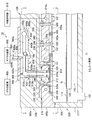
- FIG. 3 is an enlarged longitudinal sectional view (3-0, 0′-3 section) of a part of the plasma processing apparatus according to the first embodiment of the present invention.
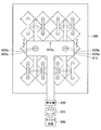
- FIG. 2 is a view (1-1 cross section) showing the ceiling surface of the plasma processing apparatus according to the same embodiment. It is the figure which showed the waveguide, microwave source, etc. which are arrange
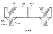
- FIG. 4D is a view (4-4 cross section) showing a connection portion between the waveguide and the coaxial waveguide according to the embodiment.
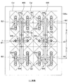
- FIG. 3 is a plan view (2-2 cross section) showing the coaxial pipe distributor and the branch structure according to the same embodiment. It is a top view of the coaxial pipe distributor which concerns on the same embodiment.
- FIG. 1 is an enlarged vertical cross-sectional view (a cross section taken along 3-0, 0′-3 shown in FIGS. 2 and 5) of a part of the microwave plasma processing apparatus 10 according to the present embodiment.
- FIG. 2 is a cross section along line 1-1 in FIG. 1 and shows the ceiling surface of the microwave plasma processing apparatus 10.
- the microwave plasma processing apparatus 10 includes a processing container 100 for plasma processing a glass substrate (hereinafter referred to as “substrate G”).
- the processing container 100 includes a container body 200 and a lid body 300.
- the container body 200 has a bottomed cubic shape with an upper portion opened, and the opening is closed by a lid 300.
- the lid body 300 includes an upper lid body 300a and a lower lid body 300b.
- An O-ring 205 is provided on a contact surface between the container main body 200 and the lower lid body 300b, whereby the container main body 200 and the lower lid body 300b are hermetically sealed to define a processing chamber.
- An O-ring 210 and an O-ring 215 are also provided on the contact surface between the upper lid 300a and the lower lid 300b, so that the upper lid 300a and the lower lid 300b are sealed.
- the container body 200 and the lid body 300 are made of a metal such as an aluminum alloy, for example, and are electrically grounded.
- a susceptor 105 (stage) for placing the substrate G is provided.
- Susceptor 105 is made of, for example, aluminum nitride.
- the susceptor 105 is supported by a support 110, and a baffle plate 115 for controlling the gas flow in the processing chamber to a preferable state is provided around the susceptor 105.
- a gas discharge pipe 120 is provided at the bottom of the processing container 100, and the gas in the processing container 100 is discharged using a vacuum pump (not shown) provided outside the processing container 100.
- the dielectric plate 305, the metal electrode 310, and the metal cover 320 are regularly arranged on the ceiling surface of the processing container 100.
- Twenty dielectric plates 305 and metal electrodes 310 are arranged at an equal pitch at a position inclined by approximately 45 ° with respect to the substrate G and the processing container 100.
- the slightly cut corners of the dielectric plate 305 are arranged adjacent to each other.
- Twelve metal covers 320 are disposed between the dielectric plate 305 and the metal electrode 310.
- a side cover 350 surrounding all the metal electrodes 310 and the metal cover 320 is also provided on the ceiling surface.
- the dielectric plate 305, the metal electrode 310, and the metal cover 320 are substantially square plates with slightly rounded corners.
- the metal electrode 310 is a flat plate provided adjacent to the dielectric plate 305 so that the dielectric plate 305 is substantially uniformly exposed from the outer edge of the metal electrode 310. With this configuration, the dielectric plate 305 is sandwiched between the inner surface of the lid 300 and the metal electrode 310 and is in close contact with the inner surface of the processing container 100.
- the metal electrode 310 is electrically connected to the inner wall of the processing container 100.
- the metal electrode 310 and the metal cover 320 are thicker than the metal cover 320 by the thickness of the dielectric plate 305. According to such a shape, the height of the ceiling surface becomes substantially equal.
- the dielectric plate 305 is made of alumina, and the metal electrode 310, the metal cover 320, and the side cover 350 are made of an aluminum alloy.
- the number of dielectric plates 305 and metal electrodes 310 is not limited to this, and can be increased or decreased by the same number.
- the dielectric plate 305 and the metal electrode 310 are fixed by screwing the convex portion of the metal electrode 310 penetrating the dielectric plate 305 to the cap nut 325 shown in FIG.
- the metal cover 320 is fixed by screwing a bolt 330 into a recess provided in the metal cover 320 while a washer 345 is interposed in the recess of the lower lid 300b.
- An O-ring 220 is provided between the cap nut 325 and the lower lid 300b, so that the gas from the main gas channel 335 is processed without passing through the gas channel 325a provided in the cap nut 325. It is prevented from being discharged into the container 100.
- a main gas flow path 335 is provided between the upper lid body 300a and the lower lid body 300b in a direction perpendicular to the paper surface.
- the main gas flow path 335 divides the gas into the gas flow paths 325 a and 330 a provided in the plurality of cap nuts 325 and the bolts 330.
- a nozzle 340 for narrowing the flow path is fitted into the inlets of the gas flow paths 325a and 330a.
- the nozzle 340 is made of ceramic or metal.
- the metal electrode 310 is provided with a gas flow path 310a communicating with the gas flow path 325a, and a plurality of gas holes hl1 are opened at the tip thereof.
- the gas cover 320a is also provided in the metal cover 320 and the side cover 350, and a plurality of gas holes hl2 are opened at the tips thereof.
- the tip surfaces of the nut 325 and the bolt 330 are not exposed on the plasma-side surfaces of the metal electrode 310, the metal cover 320, and the side cover 350 so as not to disturb the plasma distribution.
- the gas holes hl1 and the gas holes hl2 are arranged at an equal pitch.
- the gas output from the gas supply source 905 passes from the main gas channel 335 through the gas channels 325a and 330a to the first gas channel 310a in the metal electrode 310 and the second gas in the metal cover 320 and the side cover 350.
- the gas passage 320a is supplied to the processing chamber through the gas holes hl1 and hl2.
- the gas shower plate on the metal surface of the ceiling portion, it has been possible to suppress the etching of the dielectric plate surface caused by ions in the plasma and the deposition of reaction products on the inner wall of the processing vessel, It is possible to reduce contamination and particles. Further, unlike the dielectric, the metal can be easily processed, so that the cost can be greatly reduced.
- the dielectric plate 305 is exposed from between the metal electrode 310 adjacent to the dielectric plate 305 and the metal cover 320 where the dielectric plate 305 is not disposed.
- An area having the center point of the metal cover 320 adjacent to the center of one metal electrode 310 as a vertex is defined as a cell Cel, and the ceiling surface is virtually defined as an equal area.
- 20 cells are regularly arranged in the same pattern with the cell Cel as a unit. Each cell Cel is a square.
- the microwave emitted from the dielectric plate 305 propagates through the surfaces of the metal electrode 310 and the metal cover 320 while distributing power in half as a surface wave.
- the surface wave propagating between the metal surface on the inner surface of the processing vessel and the plasma is referred to as a metal surface wave.
- a groove 340 surrounding all the metal electrodes 310, the dielectric plate 305, the metal cover 320, and the side cover 350 is provided in a rectangular shape. It suppresses that the metal surface wave which propagates a ceiling surface propagates outside groove 340.
- the groove 340 may be single as in the present embodiment, or may be double or triple.
- the refrigerant supply source 910 shown in FIG. 1 is connected to the refrigerant pipe 910a inside the lid body 300, and the refrigerant supplied from the refrigerant supply source 910 circulates in the refrigerant pipe 910a and returns to the refrigerant supply source 910 again. By returning, the heating of the lower lid 300b of the lid 300 is mainly suppressed.
- the microwave source 900 outputs a 915 MHz microwave.
- the lid 300 is embedded with a coaxial tube that transmits microwaves.
- An inner conductor 610 a is inserted into the outer conductor 610 b of the first coaxial waveguide 610 formed by digging the lid 300.
- the end of the first coaxial waveguide 610 is in contact with the dielectric plate 305.
- the plurality of first coaxial waveguides 610 are provided on the plurality of dielectric plates 305 on a one-to-one basis, thereby transmitting microwaves to the plurality of dielectric plates 305.
- a second coaxial waveguide 620 directed to the microwave source 900 is connected to the main tube 700 of the coaxial distributor.
- a Teflon ring 800 (Teflon is a registered trademark) is provided at a connection portion between the second coaxial waveguide 620 and the main pipe 700.
- the inner conductor 620a of the second coaxial waveguide 620 passes through the Teflon ring 800.
- the Teflon ring 800 fixes the inner conductor 620a to the outer conductor 620b and suppresses reflection when microwaves are transmitted.
- the inner conductor of each coaxial tube is made of copper with good heat conduction.
- An O-ring 225 is provided on the contact surface between the lower cover body 300 b on the outer periphery of the first coaxial waveguide 610 and the dielectric plate 305, so that the atmosphere in the first coaxial waveguide 610 enters the processing vessel 100. There is no such thing.
- a T-branch waveguide 915 is disposed above the lid 300. 4 is a cross-sectional view taken along line 4-4 of FIG. As shown in FIG. 4, the T-branch waveguide 915 is connected to two second coaxial waveguides 620 via two tapered coaxial waveguide converters 605. A matching rod-shaped member 915a is provided at the center back of the branch portion of the T-branch waveguide 915 so that microwaves can be transmitted favorably from the T-branch waveguide 915 to each second coaxial waveguide 620. It has become.
- the microwave is output from the microwave source 900, matched between the power supply side and the load side by the matching unit 920, and transmitted to each coaxial waveguide 620 while suppressing reflection by the tapered coaxial waveguide converter 605.
- an isolator 925 is provided between the microwave source 900 and the matching unit 920 to prevent a reflected wave from returning to the microwave source 900 even when the matching is not sufficiently achieved.
- the microwave plasma processing apparatus 10 partitions the ceiling surface into 20 cells Cel, and processes a G4.5 size substrate (920 mm ⁇ 730 mm).
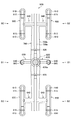
- two coaxial pipe distributors 600 for distributing and transmitting the microwaves transmitted through the transmission line to the plurality of first coaxial pipes 610 are embedded side by side in the upper lid 300a.
- the coaxial pipe distributor 600 includes a main pipe 700, a second coaxial pipe 620, a third coaxial pipe 630, a fourth coaxial pipe 640, and a fifth coaxial pipe 650.
- the coaxial pipe distributor 600 has a first branch structure B1 and a second branch structure B2 connected to the main pipe 700, the second coaxial pipe 620, and the plurality of first coaxial pipes 610, respectively.
- the main pipe 700 corresponds to a main coaxial pipe connected to the second coaxial pipe 620, the first branch structure B1, and the second branch structure B2.
- the outer conductor 700 b of the main pipe 700 is thickest at the connection position of the second coaxial waveguide 620 and gradually becomes thinner toward the connection portion with the fourth coaxial waveguide 640.
- the thickness of the inner conductor 700a of the main pipe 700 is constant.
- the first branch structure B1 has a branch structure in which the first coaxial waveguide 610 is directly connected to the third coaxial waveguide 630 without branching.
- the first branching structure B1 connects the third coaxial waveguide 630 connected at both ends of the coaxial waveguide distributor 600 to one first coaxial waveguide 610 without branching.
- the second branch structure B2 has a branch structure in which two first coaxial pipes 610 are connected to both ends of a fifth coaxial pipe 650 that is T-branched from the fourth coaxial pipe 640. That is, in the second branch structure B2, the fourth coaxial waveguide 640 coupled to both sides of the coaxial waveguide distributor 600 is T-branched and coupled to the two first coaxial waveguides 610, respectively.
- the first branch structure B1 and the second branch structure B2 are alternately connected to the main pipe 700.
- the first branch structure B1 and the second branch structure B2 are connected to the coaxial pipe distributor 600 symmetrically with respect to the second coaxial pipe 620.
- the second coaxial waveguide 620 is connected to the main tube 700 at the center of the coaxial waveguide distributor 600, the connection position is not limited to this.
- two identical branch structures are connected to one connecting portion. Different branch structures may be connected, or a number of branch structures other than two may be connected.
- the inner conductor 700a and the inner conductor 640a, and the inner conductor 700a and the inner conductor 630a are vertical in this embodiment, but may not be vertical.
- a tapered first dielectric 610c is embedded in the first coaxial tube 610 (coaxial tube having the first branch structure) shown in FIG.
- the tapered first dielectric 610c is interposed between the inner conductor 610a and the outer conductor 610b of the first coaxial waveguide 610, and is connected to the third coaxial waveguide 630 from the connecting portion of the first coaxial waveguide 610. It is formed and arranged in a reverse taper shape toward the lower end.
- the space of the outer conductor is large, and the inner conductor is slightly rounded. This suppresses the reflection of the microwave at the branch portion and fixes the tapered first dielectric 610c.
- the tapered first dielectric 610c is formed of a dielectric such as quartz, alumina, or yttria.
- the characteristic impedance of the first coaxial waveguide 610 can be converted by forming the first dielectric 610c into a tapered shape.
- the first dielectric 610c can adjust the phase of the microwave transmitted through the first coaxial waveguide 610 by adjusting the length thereof. Characteristic impedance conversion and phase adjustment will be described later.
- the space between the inner conductor and the outer conductor at the upper part of the connecting portion of the first coaxial waveguide 610 is supported by a Teflon rod 805.
- a Teflon ring 810 is also provided in the vicinity of the distal end of the first coaxial waveguide 610 so that the inner conductor 610a is supported by the outer conductor 610b.
- the fifth coaxial waveguide 650 is similarly provided with a Teflon ring 815 so that the inner conductor 650a is supported by the outer conductor 650b.
- the Teflon rod 805 and the Teflon rings 810 and 815 are made of a dielectric such as Teflon (registered trademark), glass-filled Teflon, quartz, alumina, and yttria.
- a Teflon ring 820 is also provided between the inner conductor 700a and the outer conductor 700b of the main pipe 700.
- the Teflon ring 820 is made of Teflon.
- the Teflon ring 820 supports the inner conductor 700a on the outer conductor 700b and adjusts the electrical length of the microwave according to the relative dielectric constant and thickness thereof.
- the Teflon ring 820 is not limited to Teflon, and may be formed of a dielectric such as glass-filled Teflon, quartz, alumina, or yttria.
- ⁇ Impedance of plasma as a load varies depending on process conditions. For this reason, it is impossible in principle to always make the reflection from the load zero. Even if there is reflection from the load, it is necessary to design a branch line that supplies microwaves of the same amplitude and phase to each cell. For this reason, in order to make the voltage and phase of the microwaves in the connecting part C1 and the connecting part C2 coincide with each other even if there is reflection from the load, the electrical length between the connecting part C1 and the connecting part C2 is an integral multiple of 2 ⁇ rad (this embodiment 1 in the form) (see FIGS. 5 and 8).
- the first branch structure B1 and the second branch structure B2 are provided, and the electrical lengths thereof are different. Therefore, the phase of the microwaves at the connection portion C1 and the connection portion C2 is different. The phase of the microwave supplied to each cell cannot be made the same only by making them coincide. For this reason, the first branch structure B1 is provided with a phase adjustment unit described later.
- the first coaxial waveguide 610 connected to the tip of the first branch structure B1 and the first coaxial waveguide 610 connected to the tip of the second branch structure B2 are connected to the plurality of metal electrodes 310 at equal pitches, respectively.
- Each pitch is 4 ⁇ n / 3 rad (n is an integer) based on the electrical length of the main pipe 700.
- a Teflon 820 is interposed between the inner conductor 700a and the outer conductor 700b of the main pipe 700 so that the electrical length between the connecting portion C1 and the connecting portion C2 becomes 2 ⁇ rad. I have to.
- the cell pitch can be determined relatively freely by such adjusting means.
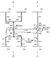
- FIG. 8 is a diagram schematically showing the first branch structure B1 and the second branch structure B2.
- the second branch structure B2 on the right side of the input unit In is omitted.
- the first dielectric 610c converts the characteristic impedance to an appropriate value while suppressing the reflection of the microwave with the taper shape and length, and simultaneously adjusts the electrical length of the first branch structure B1 and supplies it to all the cells. Align the phase of microwaves to be transmitted.
- the characteristic impedance of the coaxial tube is expressed by the following equation (1).
- epsilon r is the effective dielectric constant of the first dielectric 610c
- b is the diameter of the outer conductor 610b of the first coaxial waveguide 610
- a is a diameter of the inner conductor 610a of the first coaxial waveguide 610 is there.
- the effective relative dielectric constant ⁇ r of the first dielectric 610c is changed without changing the diameter of the outer conductor 610b and the diameter of the inner conductor 610a.
- the first dielectric 610c is formed in a reverse taper shape so that the upper part of the first dielectric 610c is thick and the lower part is thin.
- quartz having a relative dielectric constant ⁇ r of 3.8 is used for the first dielectric 610c.
- the relative dielectric constant between the inner and outer conductors is approximately 3.8. Will be equal.
- the lower the first coaxial pipe 610 is, the higher the proportion of air in the material filling the space between the inner and outer conductors than in quartz. Therefore, the effective relative dielectric constant ⁇ r between the inner and outer conductors of the first coaxial waveguide 610 gradually becomes smaller than 3.8.
- the characteristic impedance Z 0 when there is no change in the variables a and b and the effective relative dielectric constant ⁇ r gradually decreases, the characteristic impedance Z 0 gradually increases. Therefore, the characteristic impedance Z 0 increases from the top to the bottom of the first dielectric 610c. In this way, the characteristic impedance of the microwave can be converted to a desired value using the first dielectric 610c.
- the characteristic impedance (30 ⁇ ) of the lower part of the first coaxial waveguide 610 where the first dielectric 610c is arranged is changed to the upper part by the characteristic impedance conversion / phase adjustment unit realized by the first dielectric 610c. It is converted to characteristic impedance (20 ⁇ ).
- the higher the relative dielectric constant the more delayed the microwave phase. Therefore, the longer the taper portion of the first dielectric 610c, the longer the phase of the microwave. Using this principle, the electrical length of the first branch structure B1 is adjusted.
- the phase adjustment of the microwave and the characteristic impedance conversion are simultaneously performed by forming quartz in a tapered shape. Note that, depending on the design, there may be no shift in the phase of the microwave supplied to each cell without the phase adjustment unit. In that case, phase adjustment is not necessary. In addition, when it is necessary to adjust only the phase without converting the characteristic impedance, the dielectric 610c may be straight instead of tapered.
- the inner conductor 610a or the outer conductor 610b may be tapered and the space between the inner and outer conductors may be filled with a dielectric such as quartz.
- the first dielectric 610c does not need to be tapered, and the processing cost can be reduced.
- the characteristic impedance conversion / phase adjustment unit may be provided in the second branch structure B2.
- the second branch structure B2 is connected to the four metal electrodes 310 while branching into two.
- the first branch structure B1 is directly connected to one metal electrode 310 without branching. In this way, when the branch destination loads are different, the microwave power supplied from the input unit In to the left and right main pipes 700 and the microwave power supplied to the upper and lower coaxial pipes are distributed 4: 1. Otherwise, the microwave power cannot be equally divided into each cell (metal electrode 310).
- the characteristic impedance of the main pipe 700 extending left and right from the input part In is set to 75 ⁇ , and the characteristic impedance of the fourth coaxial pipe extending vertically from the input part In is viewed. Are each 300 ⁇ . This can be calculated as follows.
- the combined impedance of the four branch destinations connected in parallel may be matched with the characteristic impedance of the second coaxial waveguide 620 that is the branch source.
- the characteristic impedance of each coaxial tube is determined so that the left and right impedances viewed from the input unit In are 75 ⁇ and the upper and lower impedances viewed from the input unit In are 300 ⁇ .
- the characteristic impedance of the lower part of the first coaxial waveguide 610 connected to the metal electrode 310 of each cell is set to 20 ⁇ , for example.
- a step is provided in the inner conductor 610a of the first coaxial waveguide 610 so that the characteristic impedance of the upper portion of the first coaxial waveguide 610 is 30 ⁇ . Further, by adjusting the length of the lower portion of the first coaxial waveguide 610, the reflection is suppressed to be smaller. Further, the characteristic impedance of the fifth coaxial waveguide 650 is set to 30 ⁇ , which is equal to the characteristic impedance of the upper portion of the first coaxial waveguide 610.
- the characteristic impedance of the main pipe 700 in the vicinity of the input unit In is set to 75 ⁇ and the load impedance is matched with this value.
- the outer conductor 700b of the main pipe 700 is gradually tapered to have a tapered shape, and the characteristic impedance of the main pipe 700 in the vicinity of the connecting portion with the second branch structure is 60 ⁇ . This is for adjusting the electrical length of the fourth coaxial waveguide 640 to a desired length, but the main tube 700 is not necessarily tapered in this way.
- the electrical length from the end portion of the main pipe 700 to the connecting portion of the branch structure closest to the end portion is approximately equal to an odd multiple (here, 1 time) of ⁇ / 2 rad.
- one end can be regarded as a distributed constant line short-circuited.
- the distributed constant line having the electrical length of ⁇ / 2 rad with one end short-circuited appears to have an infinite impedance when viewed from the other end. Therefore, the part from the end of the main pipe 700 to the connecting part does not exist for microwave transmission, and the transmission line can be easily designed.
- the combined impedance of the two fifth coaxial waveguides 650 viewed from the branch portion T is 1 ⁇ 2 of the characteristic impedance 30 ⁇ of the fifth coaxial waveguide 650.
- the characteristic impedance of the lower portion of the first coaxial waveguide 610 connected to the metal electrode 310 of each cell is set to 20 ⁇ in order to suppress electric field concentration and reflection from the load side. To do.
- a step is provided in the inner conductor 610a of the first coaxial waveguide 610 so that the characteristic impedance of the upper portion of the first coaxial waveguide 610 is 30 ⁇ , and the length of the lower portion is adjusted so that no reflection occurs. To do.
- the characteristic impedance conversion / phase adjustment unit of the first coaxial waveguide 610 is actually provided with the first dielectric 610c having a reverse taper shape between the inner conductor 610a and the outer conductor 610b. It becomes the composition.
- the characteristic impedance can be gradually reduced from the output side above the first coaxial waveguide 610 toward the input side.
- the characteristic impedance on the output side above the first coaxial waveguide 610 can be set to 30 ⁇ , and the characteristic impedance on the input side can be set to 20 ⁇ .
- the impedance Z in when the upper and lower coaxial tubes are viewed from the input unit In must be 300 ⁇ .
- the third coaxial waveguide 630 functions as an impedance converter for satisfying these impedance relationships, and the electrical length and characteristic impedance are designed as follows.
- the electrical length of the third coaxial waveguide 630 is set to ⁇ / 2 rad.
- the characteristic impedance Z c3 of the third coaxial waveguide 630 is obtained by the following equation. ... (5)
- Z c1 is the characteristic impedance of the upper part of the characteristic impedance converter of the coaxial tube 610.
- FIG. 9 shows the result of expressing the state of incidence, reflection, and transmission of microwaves at each port shown in FIG. 7 using S parameters.
- the result is shown in FIG. S11 indicates a microwave input from port 1 and output from port 1. That is, S11 indicates the reflected wave and phase (inside parentheses) of the microwave output from the port 1. According to this, the reflection of the microwave from the port 1 is “0.003” and is almost “0”, and it can be seen that the reflection is extremely small.
- S12 to S16 are verified.
- S12 to S16 indicate microwaves that are input from the port 1 of FIG. 7 and output from the ports 2 to 6, respectively.
- the amplitudes of the microwaves output from the ports 2 to 6 are “0.446” or “0.447”, which are almost the same.
- the phases of the microwaves output from the ports 2 to 6 are completely in agreement with “ ⁇ 119 °”.
- microwaves having the same amplitude and phase can be supplied into the processing container even in the transmission paths having different branch structures such as the first branch structure B1 and the second branch structure B2.
- the design of the microwave plasma processing apparatus 10 that is relatively not limited by the substrate size, the number of cells (that is, the number of branches) can be realized.
- the arrangement position of the first coaxial pipe 610 can be optimized.
- the shape of the cell Cel can be made square with respect to the substrate G having a predetermined size, and the area of the cell Cel can be made relatively large.
- the substrate can be subjected to uniform plasma treatment, and the cost can be reduced by making the area of the cell Cel relatively large.
- the second branch structure is arranged in the second coaxial waveguide (input part In), and the first branch structure B1 is coaxial on both sides thereof.
- the pipe distributor 600 is arranged symmetrically with respect to the main pipe 700.
- first branch structure B1 and the second branch structure B2 are connected to the main pipe 700 in the order of the second branch structure B2 and the first branch structure B1 from the second coaxial waveguide (input part In) toward both sides. It is connected.
- the length from the input part In to the first branch structure B1 is freely determined.
- the distance from the connecting portion of the first branch structure B1 to the connecting portion of the second branch structure B2 is 2 ⁇ nrad (n is an integer).
- the first branch structure B1 is further connected to the outermost side of the coaxial waveguide distributor 600 shown in FIG. 10C.
- the length from the input part In to the first branch structure B1 is freely determined.
- the distance between the connecting portion of the first branch structure B1 and the connecting portion of the second branch structure B2 is 2 ⁇ nrad (n is an integer). Thereby, the microwave of the same amplitude can be supplied to each cell.
- the allowable frequency range of the microwave source 900 is determined based on the characteristics of the magnetron, and is about ⁇ 1% of the reference frequency for the one pitch management shown in FIGS. 10A to 10C. On the other hand, for the two pitch management shown in FIG. 10D and FIG. 10E, the allowable frequency range of the microwave source 900 is about ⁇ 0.5% of the reference frequency, and FIG. ”To FIG. 10“ c ”.
- the apparatus shown in FIG. 10 “a” to FIG. 10 “c” having four, five, or six horizontal cells has the number of FIG. 10 “d” and seven or eight horizontal cells shown in FIG. Management is easier than the apparatus of FIG. 10 “e”, and it is easy to distribute the microwaves more evenly.
- the phase adjustment unit may not be provided at the same position as the characteristic impedance conversion unit.
- the phase adjustment unit may adjust only the phase.
- the phase adjustment unit can also be provided in a coaxial tube other than the first coaxial tube.
- the microwave source 900 that outputs a 915 MHz microwave is described, but a microwave source that outputs a microwave such as 896 MHz, 922 MHz, and 2.45 GHz may be used.
- the microwave source is an example of an electromagnetic wave source that generates an electromagnetic wave for exciting plasma, and includes a magnetron and a high-frequency power source as long as the electromagnetic wave source outputs an electromagnetic wave of 100 MHz or higher.
- the plasma processing apparatus is not limited to the above-described microwave plasma processing apparatus, and plasma that finely processes an object to be processed by plasma, such as a film forming process, a diffusion process, an etching process, an ashing process, and a plasma doping process. Any processing device may be used.
- the plasma processing apparatus can process a large-area glass substrate, a circular silicon wafer, or a square SOI (Silicon On Insulator) substrate.
- a large-area glass substrate a circular silicon wafer, or a square SOI (Silicon On Insulator) substrate.
Landscapes
- Physics & Mathematics (AREA)
- Engineering & Computer Science (AREA)
- Plasma & Fusion (AREA)
- Chemical & Material Sciences (AREA)
- Analytical Chemistry (AREA)
- Electromagnetism (AREA)
- Spectroscopy & Molecular Physics (AREA)
- Plasma Technology (AREA)
- Chemical Vapour Deposition (AREA)
- Drying Of Semiconductors (AREA)
Abstract
Description
<第1実施形態>
[プラズマ処理装置の構成]
(全体構成)
(天井面の構成)
(伝送線路)
(同軸管分配器と分岐構造)
(第1の誘電体)
[各分岐構造のインピーダンス整合及び位相調整機構]
(特性インピーダンス変換/位相調整部)
(インピーダンス整合)
(第2の分岐構造のインピーダンス整合)
(第1の分岐構造のインピーダンス整合)
[効果の例]
<第1実施形態の変形例>
[変形例1に係る分岐構造]
[変形例2に係る分岐構造]
[変形例3に係る分岐構造]
[変形例4に係る分岐構造]
[変形例5に係る分岐構造]
[変形例6に係る分岐構造]
[プラズマ処理装置の構成]
まず、本発明の第1実施形態にかかるマイクロ波プラズマ処理装置の構成について、図1及び図2を参照しながら説明する。図1は、本実施形態に係るマイクロ波プラズマ処理装置10の一部を拡大した縦断面(図2及び図5に示した3-0,0’-3断面)図である。図2は、図1の1-1断面であり、マイクロ波プラズマ処理装置10の天井面を示している。
図1に示したように、マイクロ波プラズマ処理装置10は、ガラス基板(以下、「基板G」という。)をプラズマ処理するための処理容器100を有している。処理容器100は、容器本体200と蓋体300とから構成される。容器本体200は、その上部が開口された有底立方体形状を有していて、その開口は蓋体300により閉塞されている。蓋体300は、上部蓋体300aと下部蓋体300bとから構成されている。容器本体200と下部蓋体300bとの接触面にはOリング205が設けられていて、これにより容器本体200と下部蓋体300bとが密閉され、処理室が画定される。上部蓋体300aと下部蓋体300bとの接触面にもOリング210及びOリング215が設けられていて、これにより、上部蓋体300aと下部蓋体300bとが密閉されている。容器本体200及び蓋体300は、たとえば、アルミニウム合金等の金属からなり、電気的に接地されている。
図2を参照すると、処理容器100の天井面には、誘電体板305、金属電極310及び金属カバー320が規則的に配置されている。誘電体板305及び金属電極310は、基板Gや処理容器100に対して概ね45°傾いた位置に等ピッチで20枚配置される。誘電体板305のわずかに削られた角部同士は隣接して配置される。金属カバー320は、誘電体板305及び金属電極310の間に12枚配置される。
次に、マイクロ波を伝送する伝送線路について説明する。マイクロ波源900は、915MHzのマイクロ波を出力する。蓋体300には、マイクロ波を伝送させる同軸管が埋め込まれている。蓋体300を掘り込んで形成された第1の同軸管610の外部導体610bには、内部導体610aが挿入されている。第1の同軸管610の端部は、誘電体板305に当接している。このようにして、複数の第1の同軸管610は、複数の誘電体板305に一対一に設けられ、これにより、マイクロ波を複数の誘電体板305に伝送する。
図5は、図1の2-2断面図である。本実施形態に係るマイクロ波プラズマ処理装置10は、天井面を20のセルCelに区画し、G4.5サイズの基板(920mm×730mm)を処理する。
図1に示した第1の同軸管610(第1の分岐構造の同軸管)には、テーパ状の第1の誘電体610cが埋め込まれている。テーパ状の第1の誘電体610cは、第1の同軸管610の内部導体610aと外部導体610bとの間に介在され、第3の同軸管630との連結部分から第1の同軸管610の下端部に向かって逆テーパ状に形成及び配置される。第3の同軸管630と第1の同軸管610との連結部分では、外部導体の空間が大きく、かつ内部導体に多少の丸みが形成されている。これにより、分岐部分でのマイクロ波の反射を抑えるとともに、テーパ状の第1の誘電体610cを固定する。テーパ状の第1の誘電体610cは、石英、アルミナ、イットリア等の誘電体から形成される。
次に、図8を参照しながら、各分岐構造のインピーダンス整合及び位相調整機構について説明する。図8は、第1の分岐構造B1及び第2の分岐構造B2を模式的に示した図である。図8では、入力部In右側の第2の分岐構造B2は省略されている。
第1の誘電体610cは、テーパ形状及び長さでマイクロ波の反射を抑えつつ特性インピーダンスを適切な値に変換すると同時に、第1の分岐構造B1の電気長を調整して全てのセルに供給されるマイクロ波の位相を揃える。

以上の特性インピーダンス変換/位相調整部の機能を踏まえて、本実施形態における第1の分岐構造B1及び第2の分岐構造B2とのインピーダンス整合について説明する。
P1(横の同軸管に供給される電力)=V2(入力部Inの電圧)/R1(横の同軸管を見た抵抗)
P2(縦の同軸管に供給される電力)=V2(入力部Inの電圧)/R2(縦の同軸管を見た抵抗)
P1/P2=4/1=R2/R1・・・(2)
1/(1/R1+1/R1+1/R2+1/R2)=30Ω・・・(3)
まず、第2の分岐構造B2側のインピーダンス整合について説明する。電界集中と負荷側からの反射を抑えるために、各セルの金属電極310に繋がる第1の同軸管610の下部の特性インピーダンスを、たとえば20Ωに設定する。これに対して、第1の同軸管610の上部の特性インピーダンスを30Ωにするように第1の同軸管610の内部導体610aに段差を設ける。また、第1の同軸管610の下部の長さを調整することにより、反射をより小さく抑える。また、第5の同軸管650の特性インピーダンスを第1の同軸管610の上部の特性インピーダンスと等しい30Ωにする。

ここで、Zc7は主管700の(分岐部C近傍の)特性インピーダンス、Zc5は同軸管650の特性インピーダンスである。式(4)にZc7=60Ω、Zc5=30Ωを代入すると、Zc4=42.4Ωとなる。
次に、第1の分岐構造B1側のインピーダンス整合について説明する。第2の分岐構造のインピーダンス整合の場合と同様に、電界集中と負荷側からの反射を抑えるために、各セルの金属電極310に繋がる第1の同軸管610の下部の特性インピーダンスを20Ωに設定する。これに対して、第1の同軸管610の上部の特性インピーダンスを30Ωにするように第1の同軸管610の内部導体610aに段差を設けるとともに、反射が生じないように下部の長さを調整する。
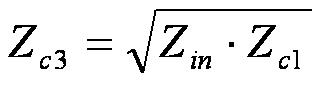
ここで、Zc1は同軸管610の特性インピーダンス変換部上部の特性インピーダンスである。式(5)にZin=300Ω、Zc1=20Ωを代入すると、Zc3=77.4Ωとなる。
以上のように、分岐構造の最適化を図った同軸管分配器600分岐回路について、反射の状態及び位相の状態をシミュレーションにより求めた。図9は、図7に示す各ポートにおけるマイクロ波の入射、反射、透過の状態をSパラメータで表記した結果である。その結果を図9に示す。S11は、ポート1から入力してポート1から出力されるマイクロ波を示している。すなわち、S11は、ポート1から出力されるマイクロ波の反射波及び位相(かっこ内)を示す。これによれば、ポート1からのマイクロ波の反射は、「0.003」とほぼ「0」であり、反射が極めて小さいことが分かる。
[変形例1に係る分岐構造]
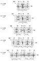
図10“b”に示したように、今まで述べてきた10分岐(セル数:5×2=10)の分岐構造を基本として、図10“a”、図10“c”~図10“e”等の変形例が考えられる。たとえば、図10“a”に示した変形例1に係る分岐構造では、第2の同軸管(入力部In)に第2の分岐構造が配置され、その両側に第1の分岐構造B1が同軸管分配器600の主管700に対して対称的に配置される。つまり、第1の分岐構造B1及び第2の分岐構造B2は、第2の同軸管(入力部In)から両側に向けて第2の分岐構造B2、第1の分岐構造B1の順に主管700に連結されている。この場合、セル数は、8(=6×2)となる。
図10“c”に示した変形例2に係る分岐構造では、第1の分岐構造B1及び第2の分岐構造B2は、同軸管分配器600の主管700に対して対称的に配置される。つまり、第1の分岐構造B1及び第2の分岐構造B2は、第2の同軸管(入力部In)から両側に向けて第1の分岐構造B1、第2の分岐構造B2の順に主管700に連結されている。この場合、セル数は、12(=6×2)となる。
図10“d”に示した変形例3に係る分岐構造では、第1の分岐構造B1を中心として、第2の分岐構造B2、第1の分岐構造B1が入力部Inの両側に交互に出現する。この場合、セル数は、14(=7×2)となる。その際、第1の分岐構造B1の連結部と第2の分岐構造B2の連結部との距離は、すべて2πnrad(nは整数)にする。これにより、同一振幅のマイクロ波を各セルに供給することができる。
図10“e”に示した変形例4に係る分岐構造では、図10“c”の同軸管分配器600に対して、最も外側に、さらに第1の分岐構造B1が連結されている。この場合、セル数は、16(=8×2)となる。この場合にも、入力部Inから第1の分岐構造B1までの間の長さは自由に定められる。第1の分岐構造B1の連結部と第2の分岐構造B2の連結部との距離は、2πnrad(nは整数)にする。これにより、同一振幅のマイクロ波を各セルに供給することができる。
図11に示した変形例5では、図10“c”の同軸分配器600の構成が並列に4つ並べられている。これによれば、太陽電池基板サイズ1.20m×1.64mに適したプラズマ励起領域を確保することができる。
図12に示した変形例6では、図10“b”の同軸分配器600の構成が縦横に4つずつ合計8つ並べられている。これによれば、太陽電池基板サイズ1.64m×2.08mに適したプラズマ励起領域を確保することができる。
Claims (19)
- 電磁波によりガスを励起させて被処理体をプラズマ処理するプラズマ処理装置であって、
処理容器と、
電磁波を出力する電磁波源と、
前記電磁波源から出力された電磁波を伝送する伝送線路と、
前記処理容器の内面に設けられ、電磁波を前記処理容器内に放出する複数の誘電体板と、
前記複数の誘電体板に隣接し、電磁波を前記複数の誘電体板に伝送する複数の第1の同軸管と、
前記伝送線路を伝送した電磁波を前記複数の第1の同軸管に分配して伝送する1段又は2段以上の所定の段数を有する複数の同軸管分配器と、を備え、
前記複数の同軸管分配器のうち少なくとも一つは、他の同軸管分配器と段数が異なることを特徴とするプラズマ処理装置。 - 前記複数の同軸管分配器のうち少なくとも一つは段数が1段であり、他の同軸管分配器の段数は2段である請求項1に記載のプラズマ処理装置。
- 電磁波によりガスを励起させて被処理体をプラズマ処理するプラズマ処理装置であって、
処理容器と、
電磁波を出力する電磁波源と、
前記電磁波源から出力された電磁波を伝送する伝送線路と、
前記処理容器の内面に設けられ、電磁波を前記処理容器内に放出する複数の誘電体板と、
前記複数の誘電体板に隣接し、電磁波を前記複数の誘電体板に伝送する複数の第1の同軸管と、
前記伝送線路を伝送した電磁波を前記複数の第1の同軸管に分配して伝送する1段又は2段以上の同軸管分配器と、を備え、
前記同軸管分配器のうち少なくとも一段は、前記複数の第1の同軸管にそれぞれ連結される異なる構成の分岐構造と、前記異なる構成の分岐構造が連結する主同軸管と、を含むプラズマ処理装置。 - 前記主同軸管に連結される入力部を有する第2の同軸管を有する請求項3に記載のプラズマ処理装置。
- 前記分岐構造は、第1の分岐構造及び第2の分岐構造の2種類を有する請求項3に記載のプラズマ処理装置。
- 前記第1の分岐構造は、分岐せずに前記複数の第1の同軸管の少なくともいずれかに連結される請求項5に記載のプラズマ処理装置。
- 前記第2の分岐構造は、分岐して前記複数の第1の同軸管の少なくともいずれかに連結される請求項5に記載のプラズマ処理装置。
- 前記第2の分岐構造は、2分岐である請求項7に記載のプラズマ処理装置。
- 前記第1の分岐構造及び前記第2の分岐構造は、前記主同軸管に交互に連結される請求項5に記載のプラズマ処理装置。
- 前記第1の分岐構造及び前記第2の分岐構造は、前記第2の同軸管と前記主同軸管との連結部から前記主同軸管の両側に向かって前記主同軸管に交互に連結される請求項5に記載のプラズマ処理装置。
- 前記第1の分岐構造及び前記第2の分岐構造が前記主同軸管に連結する連結部分のピッチは、電気長で2πnrad(nは整数)である請求項5に記載のプラズマ処理装置。
- 前記第1の分岐構造及び前記第2の分岐構造が前記主同軸管に連結する連結部分のピッチは、前記第2の同軸管と前記主同軸管との連結部を除いて電気長で2πnrad(nは整数)である請求項5に記載のプラズマ処理装置。
- 前記第1の分岐構造及び前記第2の分岐構造は、前記第2の同軸管に対して対称的に前記主同軸管に連結されている請求項9に記載のプラズマ処理装置。
- 前記複数の第1の同軸管内の少なくともいずれかには、第1の誘電体が埋め込まれている請求項5に記載のプラズマ処理装置。
- 前記第1の誘電体は、テーパ状である請求項14に記載のプラズマ処理装置。
- 前記第1の誘電体は、前記第1の同軸管の内部導体と外部導体との間に介在される請求項14に記載のプラズマ処理装置。
- 前記第1の誘電体は、その形状により前記第1の同軸管の特性インピーダンスを変換する請求項14に記載のプラズマ処理装置。
- 前記第1の誘電体は、その長さにより前記第1の同軸管の電気長を調整する請求項14に記載のプラズマ処理装置。
- 前記複数の第1の同軸管は、前記複数の誘電体板に等ピッチでそれぞれ連結され、各ピッチは、前記主同軸管の電気長を基準として4πn/3rad(nは整数)である請求項3に記載のプラズマ処理装置。
Priority Applications (3)
| Application Number | Priority Date | Filing Date | Title |
|---|---|---|---|
| KR1020117016530A KR101340337B1 (ko) | 2009-01-21 | 2009-11-02 | 플라즈마 처리 장치 |
| US13/145,398 US9105450B2 (en) | 2009-01-21 | 2009-11-02 | Plasma processing apparatus |
| CN2009801553517A CN102293063A (zh) | 2009-01-21 | 2009-11-02 | 等离子体处理装置 |
Applications Claiming Priority (2)
| Application Number | Priority Date | Filing Date | Title |
|---|---|---|---|
| JP2009011455A JP5222744B2 (ja) | 2009-01-21 | 2009-01-21 | プラズマ処理装置 |
| JP2009-011455 | 2009-01-21 |
Publications (1)
| Publication Number | Publication Date |
|---|---|
| WO2010084655A1 true WO2010084655A1 (ja) | 2010-07-29 |
Family
ID=42355724
Family Applications (1)
| Application Number | Title | Priority Date | Filing Date |
|---|---|---|---|
| PCT/JP2009/068748 Ceased WO2010084655A1 (ja) | 2009-01-21 | 2009-11-02 | プラズマ処理装置 |
Country Status (6)
| Country | Link |
|---|---|
| US (1) | US9105450B2 (ja) |
| JP (1) | JP5222744B2 (ja) |
| KR (1) | KR101340337B1 (ja) |
| CN (1) | CN102293063A (ja) |
| TW (1) | TW201119520A (ja) |
| WO (1) | WO2010084655A1 (ja) |
Cited By (7)
| Publication number | Priority date | Publication date | Assignee | Title |
|---|---|---|---|---|
| GB2486953A (en) * | 2010-12-23 | 2012-07-04 | Element Six Ltd | Microwave power delivery system for plasma reactors |
| US8859058B2 (en) | 2010-12-23 | 2014-10-14 | Element Six Limited | Microwave plasma reactors and substrates for synthetic diamond manufacture |
| US8955456B2 (en) | 2010-12-23 | 2015-02-17 | Element Six Limited | Microwave plasma reactor for manufacturing synthetic diamond material |
| US9410242B2 (en) | 2010-12-23 | 2016-08-09 | Element Six Technologies Limited | Microwave plasma reactor for manufacturing synthetic diamond material |
| US9637838B2 (en) | 2010-12-23 | 2017-05-02 | Element Six Limited | Methods of manufacturing synthetic diamond material by microwave plasma enhanced chemical vapor deposition from a microwave generator and gas inlet(s) disposed opposite the growth surface area |
| US10403477B2 (en) | 2010-12-23 | 2019-09-03 | Element Six Technologies Limited | Microwave plasma reactor for manufacturing synthetic diamond material |
| US11371147B2 (en) | 2010-12-23 | 2022-06-28 | Element Six Technologies Limited | Microwave plasma reactor for manufacturing synthetic diamond material |
Families Citing this family (7)
| Publication number | Priority date | Publication date | Assignee | Title |
|---|---|---|---|---|
| JP5520455B2 (ja) * | 2008-06-11 | 2014-06-11 | 東京エレクトロン株式会社 | プラズマ処理装置 |
| JP5478058B2 (ja) * | 2008-12-09 | 2014-04-23 | 国立大学法人東北大学 | プラズマ処理装置 |
| JP2014026773A (ja) * | 2012-07-25 | 2014-02-06 | Tokyo Electron Ltd | プラズマ処理装置 |
| JPWO2015029090A1 (ja) * | 2013-08-30 | 2017-03-02 | 国立大学法人東北大学 | プラズマ処理装置およびプラズマ処理方法 |
| KR102020826B1 (ko) * | 2018-12-03 | 2019-09-11 | 주성엔지니어링(주) | 플라즈마 발생 장치 및 플라즈마 발생 방법 |
| KR102108896B1 (ko) * | 2019-09-05 | 2020-05-11 | 주성엔지니어링(주) | 플라즈마 발생 장치 및 플라즈마 발생 방법 |
| TW202514705A (zh) | 2023-05-30 | 2025-04-01 | 荷蘭商Asm Ip私人控股有限公司 | 用於將能量提供至具有多個功率信號輸入之電漿腔室的系統以及半導體處理系統 |
Citations (4)
| Publication number | Priority date | Publication date | Assignee | Title |
|---|---|---|---|---|
| JP2001192840A (ja) * | 2000-01-14 | 2001-07-17 | Sharp Corp | プラズマプロセス装置 |
| JP2005116362A (ja) * | 2003-10-08 | 2005-04-28 | Toshiba Corp | マイクロ波励起のプラズマ処理装置およびプラズマ処理方法 |
| JP2005310478A (ja) * | 2004-04-20 | 2005-11-04 | Naohisa Goto | プラズマ処理装置および処理方法、並びに、フラットパネルディスプレイの製造方法 |
| WO2008153064A1 (ja) * | 2007-06-11 | 2008-12-18 | Tokyo Electron Limited | プラズマ処理装置および処理方法 |
Family Cites Families (12)
| Publication number | Priority date | Publication date | Assignee | Title |
|---|---|---|---|---|
| EP0723386B1 (en) * | 1994-07-14 | 1999-09-22 | Sumitomo Metal Industries, Ltd. | Plasma processing device |
| US5874706A (en) * | 1996-09-26 | 1999-02-23 | Tokyo Electron Limited | Microwave plasma processing apparatus using a hybrid microwave having two different modes of oscillation or branched microwaves forming a concentric electric field |
| TW492040B (en) | 2000-02-14 | 2002-06-21 | Tokyo Electron Ltd | Device and method for coupling two circuit components which have different impedances |
| US6847003B2 (en) * | 2000-10-13 | 2005-01-25 | Tokyo Electron Limited | Plasma processing apparatus |
| JP4727057B2 (ja) * | 2001-03-28 | 2011-07-20 | 忠弘 大見 | プラズマ処理装置 |
| DE10138693A1 (de) * | 2001-08-07 | 2003-07-10 | Schott Glas | Vorrichtung zum Beschichten von Gegenständen |
| JP4188004B2 (ja) * | 2002-05-31 | 2008-11-26 | 芝浦メカトロニクス株式会社 | プラズマ処理装置及び可変パワー分配器 |
| TW200415726A (en) * | 2002-12-05 | 2004-08-16 | Adv Lcd Tech Dev Ct Co Ltd | Plasma processing apparatus and plasma processing method |
| JP2007035411A (ja) * | 2005-07-26 | 2007-02-08 | Hitachi High-Technologies Corp | プラズマ処理装置 |
| JP5213150B2 (ja) * | 2005-08-12 | 2013-06-19 | 国立大学法人東北大学 | プラズマ処理装置及びプラズマ処理装置を用いた製品の製造方法 |
| JP2008021465A (ja) | 2006-07-11 | 2008-01-31 | Tokyo Electron Ltd | プラズマ処理装置およびプラズマ処理方法 |
| JP2008305736A (ja) | 2007-06-11 | 2008-12-18 | Tokyo Electron Ltd | プラズマ処理装置、プラズマ処理装置の使用方法およびプラズマ処理装置のクリーニング方法 |
-
2009
- 2009-01-21 JP JP2009011455A patent/JP5222744B2/ja not_active Expired - Fee Related
- 2009-11-02 KR KR1020117016530A patent/KR101340337B1/ko not_active Expired - Fee Related
- 2009-11-02 CN CN2009801553517A patent/CN102293063A/zh active Pending
- 2009-11-02 US US13/145,398 patent/US9105450B2/en not_active Expired - Fee Related
- 2009-11-02 WO PCT/JP2009/068748 patent/WO2010084655A1/ja not_active Ceased
-
2010
- 2010-01-20 TW TW099101428A patent/TW201119520A/zh unknown
Patent Citations (4)
| Publication number | Priority date | Publication date | Assignee | Title |
|---|---|---|---|---|
| JP2001192840A (ja) * | 2000-01-14 | 2001-07-17 | Sharp Corp | プラズマプロセス装置 |
| JP2005116362A (ja) * | 2003-10-08 | 2005-04-28 | Toshiba Corp | マイクロ波励起のプラズマ処理装置およびプラズマ処理方法 |
| JP2005310478A (ja) * | 2004-04-20 | 2005-11-04 | Naohisa Goto | プラズマ処理装置および処理方法、並びに、フラットパネルディスプレイの製造方法 |
| WO2008153064A1 (ja) * | 2007-06-11 | 2008-12-18 | Tokyo Electron Limited | プラズマ処理装置および処理方法 |
Cited By (11)
| Publication number | Priority date | Publication date | Assignee | Title |
|---|---|---|---|---|
| GB2486953A (en) * | 2010-12-23 | 2012-07-04 | Element Six Ltd | Microwave power delivery system for plasma reactors |
| US8859058B2 (en) | 2010-12-23 | 2014-10-14 | Element Six Limited | Microwave plasma reactors and substrates for synthetic diamond manufacture |
| US8955456B2 (en) | 2010-12-23 | 2015-02-17 | Element Six Limited | Microwave plasma reactor for manufacturing synthetic diamond material |
| GB2486953B (en) * | 2010-12-23 | 2015-07-01 | Element Six Ltd | Microwave power delivery system for plasma reactors |
| US9142389B2 (en) | 2010-12-23 | 2015-09-22 | Element Six Technologies Limited | Microwave power delivery system for plasma reactors |
| US9410242B2 (en) | 2010-12-23 | 2016-08-09 | Element Six Technologies Limited | Microwave plasma reactor for manufacturing synthetic diamond material |
| US9637838B2 (en) | 2010-12-23 | 2017-05-02 | Element Six Limited | Methods of manufacturing synthetic diamond material by microwave plasma enhanced chemical vapor deposition from a microwave generator and gas inlet(s) disposed opposite the growth surface area |
| US9738970B2 (en) | 2010-12-23 | 2017-08-22 | Element Six Limited | Microwave plasma reactors and substrates for synthetic diamond manufacture |
| US10403477B2 (en) | 2010-12-23 | 2019-09-03 | Element Six Technologies Limited | Microwave plasma reactor for manufacturing synthetic diamond material |
| US11371147B2 (en) | 2010-12-23 | 2022-06-28 | Element Six Technologies Limited | Microwave plasma reactor for manufacturing synthetic diamond material |
| US11488805B2 (en) | 2010-12-23 | 2022-11-01 | Element Six Technologies Limited | Microwave plasma reactor for manufacturing synthetic diamond material |
Also Published As
| Publication number | Publication date |
|---|---|
| US20110303364A1 (en) | 2011-12-15 |
| JP2010170809A (ja) | 2010-08-05 |
| TW201119520A (en) | 2011-06-01 |
| JP5222744B2 (ja) | 2013-06-26 |
| KR101340337B1 (ko) | 2013-12-11 |
| CN102293063A (zh) | 2011-12-21 |
| KR20110094353A (ko) | 2011-08-23 |
| US9105450B2 (en) | 2015-08-11 |
Similar Documents
| Publication | Publication Date | Title |
|---|---|---|
| JP5222744B2 (ja) | プラズマ処理装置 | |
| CN101632330B (zh) | 等离子体处理装置、供电装置及等离子体处理装置的使用方法 | |
| JP5421551B2 (ja) | プラズマ処理装置及びプラズマ処理方法 | |
| JP4944198B2 (ja) | プラズマ処理装置および処理方法 | |
| TW491911B (en) | Plasma process apparatus | |
| KR102469576B1 (ko) | 플라즈마 처리 장치 | |
| JP5103223B2 (ja) | マイクロ波プラズマ処理装置およびマイクロ波プラズマ処理装置の使用方法 | |
| JP5478058B2 (ja) | プラズマ処理装置 | |
| KR101229780B1 (ko) | 플라즈마 처리 장치 및 플라즈마 처리 방법 | |
| WO2010090058A1 (ja) | プラズマ処理装置 | |
| JPWO2008153052A1 (ja) | プラズマ処理装置およびプラズマ処理装置の使用方法 | |
| JP5324137B2 (ja) | プラズマ処理装置及びプラズマ処理方法 | |
| JP5324138B2 (ja) | プラズマ処理装置及びプラズマ処理方法 | |
| KR101722307B1 (ko) | 마이크로파 방사 안테나, 마이크로파 플라즈마원 및 플라즈마 처리 장치 | |
| KR101927296B1 (ko) | 플라즈마 발생 장치 및 플라즈마 발생 방법 | |
| KR102108896B1 (ko) | 플라즈마 발생 장치 및 플라즈마 발생 방법 | |
| US20210020406A1 (en) | Plasma processing apparatus | |
| JP5656504B2 (ja) | 真空処理装置およびプラズマ処理方法 | |
| KR20180133349A (ko) | 플라즈마 발생 장치 및 플라즈마 발생 방법 |
Legal Events
| Date | Code | Title | Description |
|---|---|---|---|
| WWE | Wipo information: entry into national phase |
Ref document number: 200980155351.7 Country of ref document: CN |
|
| 121 | Ep: the epo has been informed by wipo that ep was designated in this application |
Ref document number: 09838845 Country of ref document: EP Kind code of ref document: A1 |
|
| ENP | Entry into the national phase |
Ref document number: 20117016530 Country of ref document: KR Kind code of ref document: A |
|
| NENP | Non-entry into the national phase |
Ref country code: DE |
|
| WWE | Wipo information: entry into national phase |
Ref document number: 13145398 Country of ref document: US |
|
| 122 | Ep: pct application non-entry in european phase |
Ref document number: 09838845 Country of ref document: EP Kind code of ref document: A1 |