WO2010079635A1 - 発光ダイオード駆動回路およびそれを備えた面状照明装置 - Google Patents
発光ダイオード駆動回路およびそれを備えた面状照明装置 Download PDFInfo
- Publication number
- WO2010079635A1 WO2010079635A1 PCT/JP2009/065091 JP2009065091W WO2010079635A1 WO 2010079635 A1 WO2010079635 A1 WO 2010079635A1 JP 2009065091 W JP2009065091 W JP 2009065091W WO 2010079635 A1 WO2010079635 A1 WO 2010079635A1
- Authority
- WO
- WIPO (PCT)
- Prior art keywords
- light emitting
- emitting diode
- counter
- count value
- switch
- Prior art date
- Legal status (The legal status is an assumption and is not a legal conclusion. Google has not performed a legal analysis and makes no representation as to the accuracy of the status listed.)
- Ceased
Links
Images










Classifications
-
- G—PHYSICS
- G09—EDUCATION; CRYPTOGRAPHY; DISPLAY; ADVERTISING; SEALS
- G09G—ARRANGEMENTS OR CIRCUITS FOR CONTROL OF INDICATING DEVICES USING STATIC MEANS TO PRESENT VARIABLE INFORMATION
- G09G3/00—Control arrangements or circuits, of interest only in connection with visual indicators other than cathode-ray tubes
- G09G3/20—Control arrangements or circuits, of interest only in connection with visual indicators other than cathode-ray tubes for presentation of an assembly of a number of characters, e.g. a page, by composing the assembly by combination of individual elements arranged in a matrix no fixed position being assigned to or needed to be assigned to the individual characters or partial characters
- G09G3/34—Control arrangements or circuits, of interest only in connection with visual indicators other than cathode-ray tubes for presentation of an assembly of a number of characters, e.g. a page, by composing the assembly by combination of individual elements arranged in a matrix no fixed position being assigned to or needed to be assigned to the individual characters or partial characters by control of light from an independent source
- G09G3/3406—Control of illumination source
- G09G3/342—Control of illumination source using several illumination sources separately controlled corresponding to different display panel areas, e.g. along one dimension such as lines
-
- H—ELECTRICITY
- H05—ELECTRIC TECHNIQUES NOT OTHERWISE PROVIDED FOR
- H05B—ELECTRIC HEATING; ELECTRIC LIGHT SOURCES NOT OTHERWISE PROVIDED FOR; CIRCUIT ARRANGEMENTS FOR ELECTRIC LIGHT SOURCES, IN GENERAL
- H05B45/00—Circuit arrangements for operating light-emitting diodes [LED]
- H05B45/40—Details of LED load circuits
- H05B45/44—Details of LED load circuits with an active control inside an LED matrix
- H05B45/48—Details of LED load circuits with an active control inside an LED matrix having LEDs organised in strings and incorporating parallel shunting devices
-
- G—PHYSICS
- G09—EDUCATION; CRYPTOGRAPHY; DISPLAY; ADVERTISING; SEALS
- G09G—ARRANGEMENTS OR CIRCUITS FOR CONTROL OF INDICATING DEVICES USING STATIC MEANS TO PRESENT VARIABLE INFORMATION
- G09G2310/00—Command of the display device
- G09G2310/02—Addressing, scanning or driving the display screen or processing steps related thereto
- G09G2310/024—Scrolling of light from the illumination source over the display in combination with the scanning of the display screen
-
- G—PHYSICS
- G09—EDUCATION; CRYPTOGRAPHY; DISPLAY; ADVERTISING; SEALS
- G09G—ARRANGEMENTS OR CIRCUITS FOR CONTROL OF INDICATING DEVICES USING STATIC MEANS TO PRESENT VARIABLE INFORMATION
- G09G2320/00—Control of display operating conditions
- G09G2320/02—Improving the quality of display appearance
- G09G2320/0261—Improving the quality of display appearance in the context of movement of objects on the screen or movement of the observer relative to the screen
-
- G—PHYSICS
- G09—EDUCATION; CRYPTOGRAPHY; DISPLAY; ADVERTISING; SEALS
- G09G—ARRANGEMENTS OR CIRCUITS FOR CONTROL OF INDICATING DEVICES USING STATIC MEANS TO PRESENT VARIABLE INFORMATION
- G09G2320/00—Control of display operating conditions
- G09G2320/06—Adjustment of display parameters
- G09G2320/0626—Adjustment of display parameters for control of overall brightness
- G09G2320/064—Adjustment of display parameters for control of overall brightness by time modulation of the brightness of the illumination source
-
- H—ELECTRICITY
- H05—ELECTRIC TECHNIQUES NOT OTHERWISE PROVIDED FOR
- H05B—ELECTRIC HEATING; ELECTRIC LIGHT SOURCES NOT OTHERWISE PROVIDED FOR; CIRCUIT ARRANGEMENTS FOR ELECTRIC LIGHT SOURCES, IN GENERAL
- H05B45/00—Circuit arrangements for operating light-emitting diodes [LED]
- H05B45/30—Driver circuits
- H05B45/32—Pulse-control circuits
- H05B45/325—Pulse-width modulation [PWM]
-
- H—ELECTRICITY
- H05—ELECTRIC TECHNIQUES NOT OTHERWISE PROVIDED FOR
- H05B—ELECTRIC HEATING; ELECTRIC LIGHT SOURCES NOT OTHERWISE PROVIDED FOR; CIRCUIT ARRANGEMENTS FOR ELECTRIC LIGHT SOURCES, IN GENERAL
- H05B45/00—Circuit arrangements for operating light-emitting diodes [LED]
- H05B45/30—Driver circuits
- H05B45/395—Linear regulators
Definitions
- the present invention relates to a planar illumination device, and more particularly to a light emitting diode drive circuit that drives a plurality of light emitting diodes used as a light source in a planar illumination device that emits light from the back surface of a display device.
- an image display device having a backlight such as a liquid crystal display device
- a backlight such as a liquid crystal display device
- the power consumption of the backlight can be suppressed and the image quality of the display image can be improved.
- by dividing the screen into a plurality of areas and controlling the luminance of the backlight light source corresponding to the area based on the input image in the area it is possible to further reduce power consumption and improve image quality.
- area active driving such a method of driving the display panel while controlling the luminance of the backlight light source based on the input image in the area.
- a light emitting diode In the display device employing the area active drive described above, a light emitting diode (LED) is typically employed as the light source for the backlight.
- a plurality of light emitting diode groups for example, one light emitting diode group is constituted by four light emitting diodes
- Current is applied.
- Japanese Patent Application Laid-Open No. 2005-310996 includes transistors as switches in parallel to each light emitting diode, and individual light emission by switching on / off of these transistors with a PWM signal. An invention is disclosed in which the brightness of the diode is adjusted.
- FIG. 18 is a schematic diagram illustrating a configuration example of a main part of a conventional LED driver 900.
- FIG. 18 shows a configuration for driving a light emitting diode group composed of four light emitting diodes LED1 to LED4.
- the LED driver 900 includes switches SW1 to SW4 provided in parallel to the four light emitting diodes LED1 to LED4 constituting the light emitting diode group, and the on / off states of the switches SW1 to SW4.
- a PWM control circuit 901 that controls the light emission by the PWM signals P1 to P4 and a value corresponding to a target light emission luminance (hereinafter referred to as “target luminance”) of each of the light emitting diodes LED1 to LED4 is set to a predetermined register (register REG1 described later) To REG4), and a constant current drive circuit 903 for applying a constant current to the light emitting diode group by causing an FET (field effect transistor) or the like to function as the constant current source 911. . Since the current flow of each light emitting diode is controlled by turning on / off the switches SW1 to SW4 provided in parallel to the light emitting diodes LED1 to LED4, these switches are hereinafter referred to as “bypass switches”.
- FIG. 19 is a block diagram showing the configuration of the PWM control circuit 901 in the conventional LED driver 900 and its peripheral part.
- the PWM control circuit 901 is provided in a one-to-one correspondence with the switch control circuits SC1 to SC4 for controlling the on / off states of the bypass switches SW1 to SW4 by the PWM signals P1 to P4, and the bypass switches SW1 to SW4.
- Registers REG1 to REG4, a counter 905 that counts the pulses of the PWM control circuit clock signal PCLK, and comparators CMP1 to CMP4 that compare the value of the counter with the values of the registers REG1 to REG4 are provided.
- the registers REG1 to REG4 store values corresponding to the target luminance of the corresponding light emitting diodes LED1 to LED4.
- the value of the counter 905 is reset (set to zero) by the pulse of the reset signal RST, and increases by 1 according to the pulse of the PWM control circuit clock signal PCLK.
- the bypass switches SW1 to SW4 are turned off when the value of the counter 905 is reset, and are turned on when the value of the counter 905 matches the value of the registers REG1 to REG4.
- FIG. 19 shows an example in which the counter 905 and the registers REG1 to REG4 have 12 bits. In this case, “the pulse of the PWM control circuit clock signal PCLK is 4096 (since 2 12 is 4096).
- this LED driver 900 performs PWM control for setting the luminance of each of the light emitting diodes LED1 to LED4 to the target luminance with 4096 clocks of the PWM control circuit clock signal PCLK given from the outside as one cycle. Is called. Thereby, each of the light emitting diodes LED1 to LED4 is turned on only for a desired period (period corresponding to the target luminance) in one cycle (PWM control).
- the display unit of the display device adopting area active drive is divided into a plurality of areas, and as shown in FIG. 3, a plurality of light emitting diodes L1 so that one light emitting diode corresponds to one area. , L2, L3,... Are provided on the back surface of the display unit.
- one LED driver is provided for a plurality of (four in the example shown in FIG. 20) light emitting diodes.
- the generation timing of the pulse of the reset signal RSTb given to the LED drivers LD3 and LD4 is delayed from the generation timing of the pulse of the reset signal RSTa given to the LED drivers LD1 and LD2.
- the light emitting diodes L9 to L16 are turned on at a timing later than the light emitting diodes L1 to L8.
- the plurality of light emitting diodes shown in FIG. 3 are lit in the order shown in FIG. That is, the plurality of light emitting diodes provided on the back surface of the display portion are sequentially turned on one by one.
- each light emitting diode group is arranged as shown in FIG. 20, that is, when a plurality of light emitting diodes included in each light emitting diode group are arranged in one row on the back surface of the display unit, For example, the distance between the light emitting diode and the LED driver becomes long as between the light emitting diode L1 and the LED driver LD1, and the voltage drop due to the wiring resistance between the two becomes large.
- This LED driver is configured so that the corresponding light-emitting diode is turned off by supplying a current to the above-described bypass switch. However, when the voltage drop increases, a current also flows to the light-emitting diode, and the light-emitting diode is turned on. To do.
- each light emitting diode group as shown in FIG. 21, that is, by arranging a plurality of light emitting diodes included in each light emitting diode group in two rows on the back surface of the display unit, the light emitting diodes are arranged.
- -It has been proposed to reduce the distance between LED drivers.
- the distance between the LED driver and the LED driver is not increased for any of the light-emitting diodes, and a lighting abnormality caused by a voltage drop between the light-emitting diode and the LED driver (a light-emitting diode that should originally be turned off) Occurrence of lighting) is suppressed.
- a lighting abnormality caused by a voltage drop between the light-emitting diode and the LED driver (a light-emitting diode that should originally be turned off) Occurrence of lighting) is suppressed.
- the constant current driving circuit 903 has a constant current source.
- the configuration shown in FIG. 21 has a higher advantage than the configuration shown in FIG.
- Japanese Patent Laid-Open No. 2005-310999 discloses an invention in which the brightness of each light-emitting diode is adjusted by switching the on / off state of a switch provided in parallel to each light-emitting diode as described above. Is disclosed.
- Japanese Patent Application Laid-Open No. 2001-125066 and Japanese Patent No. 3229250 disclose a liquid crystal display device which can display a high-quality moving image.
- each LED driver LD1 to LD4 emits light in the first column.
- the diodes L1 to L8 and the light emitting diodes L9 to L16 in the second column are turned on at the same timing. Accordingly, the plurality of light emitting diodes shown in FIG. 3 are lit in the order shown in FIG. That is, the plurality of light emitting diodes provided on the back surface of the display unit are sequentially turned on every two rows.
- the present invention provides an LED driver (light emitting diode driving circuit) capable of preventing a deterioration in display quality when displaying a moving image in a display device that employs a plurality of light emitting diodes as a backlight. Objective.
- a first aspect of the present invention is a light emitting diode drive circuit that drives a plurality of light emitting diodes connected in series to each other and connected in series to a constant current source for flowing a constant current, A plurality of switches connected in parallel to each of the plurality of light emitting diodes or every predetermined number, A PWM signal generation unit that generates a PWM signal for switching the on / off state of a switch connected in parallel to each light emitting diode according to the target luminance of each light emitting diode; The PWM signal generation unit generates the PWM signal based on a plurality of timing control signals for controlling a timing at which the plurality of switches are set to an on state or an off state as an initial state. To do.
- the PWM signal generator is Provided corresponding to each of the plurality of switches, and holding a luminance corresponding value that is a value corresponding to the target luminance of the light emitting diode corresponding to each switch and corresponding to the number of pulses of the clock signal given from the outside.
- a plurality of luminance correspondence value holding units A plurality of timing control signals provided so as to be respectively provided, a plurality of counters for counting the number of pulses of the clock signal and outputting as count values;
- a luminance correspondence value provided in correspondence with each of the plurality of switches and held in a luminance correspondence value holding unit corresponding to each switch, and a count value output from any one of the plurality of counters
- a plurality of switch switching units that switch the on / off state of each switch from the initial state when they match, Each switch is in an initial state based on a timing control signal given to a counter that outputs a count value compared by a switch switching unit corresponding to each switch, The count value output from each counter is reset based on a timing control signal given to each counter.
- the counter which outputs the count value compared by each switch switching part is predetermined, It is characterized by the above-mentioned.
- the PWM signal generation unit further includes a counter selection unit that selects a counter that outputs a count value to be compared by each switch switching unit based on predetermined instruction data.
- the plurality of counters includes a first counter that receives a timing control signal from the outside and a second counter other than the first counter
- the PWM signal generator is A delay control value holding unit that holds a delay control value that is a value corresponding to a difference in timing to be in an initial state for the plurality of switches and is associated with the number of pulses of the clock signal; Provided to the second counter based on the delay control value provided corresponding to the second counter and held in the delay control value holding unit and the count value output from the first counter
- a timing control signal generation unit for generating a timing control signal for The timing control signal generation unit counts output from the second counter when the delay control value held in the delay control value holding unit matches the count value output from the first counter.
- the timing control signal is generated so that the value is reset.
- It further comprises a constant current drive unit that zeros the current flowing through the constant current source when all of the plurality of switches are turned on.
- a seventh aspect of the present invention is a planar illumination device including the light emitting diode driving circuit according to any one of the first to sixth aspects of the present invention.
- the planar illumination device has a plurality of light emitting diode drive circuits,
- the plurality of light emitting diodes driven by each light emitting diode driving circuit includes a first light emitting diode group which is a light emitting diode arranged on one side with respect to the arrangement position of each light emitting diode driving circuit, and each light emitting diode driving And a second light emitting diode group which is a light emitting diode disposed on the other side with respect to the circuit arrangement position,
- the switch connected in parallel to the first light emitting diode group and the switch connected in parallel to the second light emitting diode group are set to the initial state based on different timing control signals. .
- a switch is provided for each of a plurality of light emitting diodes connected in series or in parallel for each predetermined number, and the on / off states of the switches indicate the target luminance of the corresponding light emitting diode. It is switched according to.
- the switch is set to an initial state based on a plurality of timing control signals. That is, some switches are set to an initial state at a certain timing, and some switches are set to an initial state at a different timing. Therefore, the plurality of light emitting diodes can be turned on or off at different timings (at a timing equal to the number of timing control signals).
- a part of the light emitting diode driven by the light emitting diode driving circuit is arranged on one side of the light emitting diode driving circuit in order to suppress the occurrence of lighting abnormality due to the voltage drop between the light emitting diode and the light emitting diode driving circuit.
- positioned at the other side can be lighted at a different timing.
- the light emitting diodes configured in a plurality of columns are employed as the backlight of the display device, the light emitting diodes can be turned on one by one, thereby preventing the display quality from being deteriorated when displaying a moving image. .
- the clock signal is reset based on a plurality of registers as a luminance corresponding value holding unit for storing a value corresponding to the target luminance of each light emitting diode, and a given timing control signal.
- the PWM signal generation unit includes a plurality of counters that count the number of pulses and a switch switching unit that switches on / off states of the plurality of switches, thereby preventing deterioration in display quality during moving image display.
- a light emitting diode driving circuit that can be used is realized.
- a light emitting diode driving circuit capable of preventing the display quality from being deteriorated when displaying a moving image is realized without complicating the configuration of the PWM signal generation unit.
- the counter that outputs the count value to be compared by each switch switching unit is determined based on the instruction data. Therefore, by creating the instruction data in consideration of the arrangement position of each light emitting diode, each light emitting diode can be turned on at a suitable timing. This realizes a light emitting diode driving circuit capable of preventing the display quality from being lowered during moving image display while increasing the degree of freedom regarding the positional relationship between the light emitting diode and the light emitting diode driving circuit.
- the timing control signal given to a counter other than one counter among the plurality of counters provided in the PWM signal generation unit is generated inside the PWM signal generation unit. For this reason, the external input signal which should be given to a light emitting diode drive circuit is reduced.
- the sixth aspect of the present invention when all the switches included in the light emitting diode driving circuit are turned on, the current flow in the constant current source is stopped, and the distance between the light emitting diodes is shortened. Therefore, power consumption is effectively reduced.
- a surface illumination device that achieves the same effect as any one of the first to sixth aspects of the present invention is realized.
- each light-emitting diode when one light-emitting diode drive circuit drives a predetermined number of light-emitting diodes, each light-emitting diode is arranged only on one side of the light-emitting diode drive circuit, The distance between the light emitting diode and the light emitting diode driving circuit is shortened. For this reason, the occurrence of abnormal lighting due to a voltage drop between the light emitting diode and the light emitting diode driving circuit is suppressed.
- FIG. 1 is a block diagram showing a configuration of a PWM control circuit included in an LED driver and its peripheral part in an LED backlight device according to a first embodiment of the present invention. It is a block diagram which shows the whole structure of the liquid crystal display device provided with the LED backlight apparatus which concerns on the said 1st Embodiment. In the said 1st Embodiment, it is a figure for demonstrating the correspondence of an area and a light emitting diode. In the said 1st Embodiment, it is a figure for demonstrating the drawing order to a display part. It is a schematic block diagram of the LED driver in the said 1st Embodiment. It is a figure which shows the structural example which turns off a bypass switch in the said 1st Embodiment.
- FIG. 6 is a block diagram showing a detailed configuration of a counter selection circuit in the second embodiment.
- the said 2nd Embodiment it is a figure for demonstrating determination of the value of the selection instruction
- FIG. 9 is a block diagram showing a configuration of a PWM control circuit included in an LED driver and its peripheral part in an LED backlight device according to a third embodiment of the present invention. It is a figure for demonstrating the effect in the said 3rd Embodiment. It is a schematic block diagram of the LED driver in a prior art example. It is a block diagram which shows the structure of the PWM control circuit contained in the LED driver which concerns on a prior art example, and its peripheral part. It is a figure for demonstrating a prior art example. It is a figure for demonstrating a prior art example. It is a figure which shows the lighting order of the light emitting diode in a prior art example.
- FIG. 2 is a block diagram illustrating an overall configuration of a liquid crystal display device including the LED backlight device (planar illumination device) 10 according to the first embodiment of the present invention.
- the liquid crystal display device includes an LED backlight device 10, a display control circuit 200, a source driver (video signal line driving circuit) 300, a gate driver (scanning signal line driving circuit) 400, and a display unit 500.
- the LED backlight device 10 includes a light emitting unit 110 including a plurality of light emitting diodes that constitute a backlight for irradiating light from the back surface of the display unit 500 (to the display unit 500), and a light emitting diode in the light emitting unit 110.
- the display unit 500 is divided into a plurality of areas, and area active driving is performed in which the display unit 500 is driven while controlling the luminance of the light emitting diodes based on the input image of each area.
- the display unit 500 includes a plurality (n) of source bus lines (video signal lines) SL1 to SLn, a plurality (m) of gate bus lines (scanning signal lines) GL1 to GLm, and source bus lines.
- a plurality of (n ⁇ m) pixel forming portions provided corresponding to the intersections of SL1 to SLn and gate bus lines GL1 to GLm are included. These pixel forming portions are arranged in a matrix to form a pixel array.
- Each pixel forming portion includes a TFT 50 which is a switching element in which a gate terminal is connected to a gate bus line passing through a corresponding intersection and a source terminal is connected to a source bus line passing through the intersection, and a drain terminal of the TFT 50
- a pixel capacitor Cp is constituted by a liquid crystal capacitor formed by the pixel electrode and the common electrode Ec.
- an auxiliary capacitor is provided in parallel with the liquid crystal capacitor in order to reliably hold the voltage in the pixel capacitor.
- the auxiliary capacitor is not directly related to the present invention, its description and illustration are omitted.
- a light emitting unit 110 is provided on the back surface of the display unit 500.
- the display unit 500 is divided into a plurality of areas as described above. As shown in FIG. 3, a plurality of light emitting diodes are provided in the light emitting unit 110 so that one light emitting diode corresponds to one area. ing.
- the display unit 500 including 1920 source bus lines SL1 to SL1920 and 1080 gate bus lines GL1 to GL1080, 512 (32 in the extending direction of the gate bus lines and 16 in the extending direction of the source bus lines). Area) and 512 light emitting diodes are provided in the light emitting unit 110. For these light emitting diodes, the brightness is controlled based on the input image of the area corresponding to each light emitting diode.
- the display control circuit 200 receives an image signal DAT and a timing signal group TG such as a horizontal synchronization signal and a vertical synchronization signal sent from the outside, and receives a video signal VS and a source start pulse signal for controlling image display on the display unit 500.
- the SSP, the source clock signal SCK, the gate start pulse signal GSP, the gate clock signal GCK, and a luminance control signal group KSG for controlling the luminance of the backlight (a plurality of light emitting diodes) are output.
- the source driver 300 receives the video signal VS, the source start pulse signal SSP, and the source clock signal SCK output from the display control circuit 200, and drives the driving video signals S (1) to S (S) to the source bus lines SL1 to SLn. n) is applied. Based on the gate start pulse signal GSP and the gate clock signal GCK output from the display control circuit 200, the gate driver 400 transfers the active scanning signals G (1) to G (m) to the gate bus lines GL1 to GLm. Is repeated with one vertical scanning period as a cycle.
- the LED driver 100 receives the luminance control signal group KSG output from the display control circuit 200 and drives the light emitting diode in the light emitting unit 110. Thereby, light is irradiated from the back surface of the display unit 500.
- the driving video signals S (1) to S (n) are applied to the source bus lines SL1 to SLn, and the scanning signals G (1) to G (m) are applied to the gate bus lines GL1 to GLm. Is applied, and the display unit 500 is irradiated with light from the back surface, whereby an image is displayed on the display unit 500.
- drawing is performed in the order shown in FIG. That is, paying attention to the drawing order in units of lines, drawing is performed line by line from the top to the bottom on the display screen. Focusing on the drawing order within one line, drawing is performed pixel by pixel from the left to the right on the display screen.
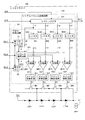
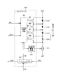
- FIG. 5 is a schematic configuration diagram of the LED driver 100 in the present embodiment.
- the LED driver 100 is provided for each light emitting diode group composed of a plurality of light emitting diodes (that is, one LED driver 100 drives a plurality of light emitting diodes). An example in which one LED driver 100 is provided will be described.
- the LED driver 100 includes bypass switches SW1 to SW4 provided in parallel to the four light emitting diodes LED1 to LED4 connected in series in the light emitting unit 110, and the bypass switches SW1 to SW4.
- a PWM control circuit 101 that controls the on / off state of SW4 by PWM signals P1 to P4, and a value corresponding to the target luminance of each of the light emitting diodes LED1 to LED4 are set in predetermined registers (registers REG1 to REG4 described later).
- the shift register 102 and a constant current drive circuit 103 for supplying a constant current to the light emitting diode group by causing the FET or the like to function as the constant current source 111 are provided.
- the display control circuit 200 includes an input data signal DIN, a clock signal CLK, a PWM control circuit clock signal PCLK, a first reset signal RST1, and a second reset signal RST2 as a luminance control signal group KSG. Given by. The role (function) of each signal will be described later.
- the shift register 102 is composed of 48 stages, and shifts the input data DIN sent by serial formation based on the pulse of the clock signal CLK (inside the shift register 102). As a result, 48-bit data is output from the shift register 102, and the 48-bit data is supplied to the PWM control circuit 101.
- the PWM control circuit 101 receives the first reset signal RST1, the second reset signal RST2, the PWM control circuit clock signal PCLK, and the 48-bit data output from the shift register 102, and outputs PWM signals P1 to P4. To do. Based on the duty ratios of the PWM signals P1 to P4, the on / off states of the bypass switches SW1 to SW4 are controlled. Also, the PWM control circuit 101 allows the current flowing through the constant current source 111 when all of the bypass switches SW1 to SW4 are turned on (that is, when all of the light emitting diodes LED1 to LED4 are turned off). The operation of the constant current drive circuit 103 is controlled so as to be zero.
- the constant current drive circuit 103 applies a constant current to the light emitting diode group by causing the FET or the like to function as the constant current source 111 as described above. However, when all of the bypass switches SW1 to SW4 are turned on, the constant current driving circuit 103 stops the current flow in the constant current source 111 based on the control signal from the PWM control circuit 101.
- the LED driver 100 controls the on / off states of the bypass switches SW1 to SW4 based on the luminance control signal group KSG sent from the display control circuit 200 according to the target luminance of the light emitting diodes LED1 to LED4.
- the luminance of the light emitting diodes LED1 to LED4 is controlled.
- a configuration in which one light emitting diode is provided for each bypass switch is described as an example.
- a plurality of light emitting diodes are provided for each bypass switch.
- the present invention can also be applied to existing configurations.
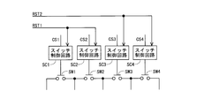
- FIG. 1 is a block diagram showing a configuration of a PWM control circuit 101 included in the LED driver 100 and its peripheral portion.
- the constant current drive circuit 103 is omitted.
- the PWM control circuit 101 includes switch control circuits SC1 to SC4 for controlling the on / off states of the bypass switches SW1 to SW4, and registers REG1 to REG4 provided to correspond to the bypass switches SW1 to SW4 on a one-to-one basis.
- a first counter C1 and a second counter C2 that count clocks, and comparators CMP1 to CMP4 that compare the values of the first counter C1 or the second counter C2 with the values of the registers REG1 to REG4, It has.
- the registers REG1 to REG4 and the shift register 102 constitute a serial / parallel conversion circuit.
- the LED driver 100 includes a clock signal CLK for causing the shift register 102 to perform a shift operation, and an input data signal DIN for storing values in the registers REG1 to REG4 according to the target brightness of the light emitting diodes LED1 to LED4.
- the PWM control circuit clock signal PCLK for causing the first counter C1 and the second counter C2 to count the number of pulses, and the first reset signal RST1 for resetting the value of the first counter C1 And a second reset signal RST1 for resetting the value of the second counter C2.
- resetting the counter value means setting the counter value to zero.
- the shift register 102 receives the serial input data signal DIN, and shifts it based on the generation timing of the pulse of the clock signal CLK.
- the shift operation refers to sequentially transferring data given bit by bit to the shift register 102 one by one in a 48-stage (48 pieces) flip-flop circuit (not shown) included in the shift register 102. It means to make it.
- 48-bit data is output in parallel from the flip-flop circuit included in the shift register 102, and the data is stored in registers REG1 to REG4 12 bits at a time.
- the data stored in the registers REG1 to REG4 are given to the comparators CMP1 to CMP4 as register data values RD1 to RD4, respectively.
- the first counter C1 and the second counter C2 count the number of pulses of the PWM control circuit clock signal PCLK.
- the value of the first counter C1 is reset based on the pulse of the first reset signal RST1
- the value of the second counter C2 is reset based on the pulse of the second reset signal RST2.
- the values of the first counter C1 and the second counter C2 increase by 1 in accordance with the pulse of the PWM control circuit clock signal PCLK.
- the value of the first counter C1 is provided as a first count value CNT1 to the comparators CMP1 and CMP2
- the value of the second counter C2 is provided as a second count value CNT2 to the comparators CMP3 and CMP4.
- the comparator CMP1 compares the first count value CNT1 and the register data value RD1, and outputs a comparison result signal CS1 indicating whether or not they match.
- the comparator CMP2 compares the first count value CNT1 with the register data value RD2, and outputs a comparison result signal CS2 indicating whether or not they match.
- the comparator CMP3 compares the second count value CNT2 and the register data value RD3, and outputs a comparison result signal CS3 indicating whether or not they match.
- the comparator CMP4 compares the second count value CNT2 with the register data value RD4, and outputs a comparison result signal CS4 indicating whether or not they match.
- the switch control circuits SC1 to SC4 respectively control the PWM signals for controlling the on / off states of the corresponding bypass switches SW1 to SW4 based on the comparison result signals CS1 to CS4 output from the corresponding comparators CMP1 to CMP4.
- P1 to P4 are output.
- the bypass switches SW1 to SW4 are turned on by the PWM signals P1 to P4
- the corresponding light emitting diodes LED1 to LED4 are turned off, and the bypass switches SW1 to SW4 are turned off by the PWM signals P1 to P4.
- the corresponding light emitting diodes LED1 to LED4 are turned on.
- the switch control circuit turns on the bypass switch, and if the logical level of the comparison result signal is low, the switch control circuit It demonstrates as what maintains a state as it is.
- a PWM signal generation unit is realized by the PWM control circuit 101
- a luminance corresponding value holding unit is realized by the registers REG1 to REG4, and switches are switched by the comparators CMP1 to CMP4 and the switch control circuits SC1 to SC4. Is realized.
- the timing control signal is realized by the first reset signal RST1 and the second reset signal RST2.
- the first counter C1 and the second counter C2 are configured with 12 bits, and the registers REG1 to REG4 provided corresponding to the respective bypass switches SW1 to SW4 are also configured with 12 bits.
- the bypass switches SW1 to SW4 are controlled to be turned on / off based on the comparison result between the first count value CNT1 or the second count value CNT2 and the register data values RD1 to RD4. Therefore, in the LED driver 100 according to the present embodiment, PWM control is performed with 4096 clocks (of the PWM control circuit clock signal PCLK) as one cycle.
- Each bypass switch SW1 to SW4 is turned off when the value of the corresponding counter is reset, and is turned on when the value of the corresponding counter matches the value of the corresponding register. Thereby, each of the light emitting diodes LED1 to LED4 is lit only for a desired period (period corresponding to the target luminance) in one cycle (of PWM control).
- the operation of the LED driver 100 will be described in detail, taking an example in which the on / off state of the bypass switch SW1 is controlled with a duty ratio of 50%, with particular attention to the bypass switch SW1.
- the duty ratio is obtained in the display control circuit 200 based on the target luminance determined according to the input image in the area corresponding to the light emitting diode LED1 whose luminance is adjusted by the bypass switch SW1.
- the content of 12-bit data is expressed in the format of “XXXX_XXXX_XXXX” (X is 0 or 1).
- a value is set in the register REG1.
- 12-bit data luminance corresponding value
- the register REG1 For example, if the duty ratio is 25 percent, data “0100 — 0000 — 0000” is stored in the register REG1, and if the duty ratio is 75 percent, data “1100 — 0000 — 0000” is stored in the register REG1.
- the registers REG2 to REG4 store 12-bit data indicating the duty ratio obtained based on the input images in the areas corresponding to the light emitting diodes LED2 to LED4, respectively.
- the bypass switch SW1 is turned off as an initial state when the first count value CNT1 is reset.
- the first reset signal RST1 is given to the switch control circuit SC1, and the switch control circuit SC1 turns off the bypass switch SW1 based on the pulse of the first reset signal RST1. It is sufficient to make the configuration as follows.
- the bypass switch SW1 is turned off, the light emitting diode LED1 is turned on.
- the bypass switch SW2 is turned off as an initial state when the first count value CNT1 is reset.
- the bypass switches SW3 and SW4 are turned off as an initial state when the second count value CNT2 is reset.
- the comparator CMP1 compares the first count value CNT1 with the register data value RD1.
- the logic level of the comparison result signal CS1 output from the comparator CMP1 becomes a high level.
- the logical level of the comparison result signal CS1 is maintained at the low level for the period until the first count value CNT1 becomes “1000 — 0000 — 0000”.
- the comparison result signal CS2 is maintained at a low level until the first count value CNT1 and the register data value RD2 coincide after the first count value CNT1 is reset.
- the comparison result signal CS3 is maintained at a low level until the second count value CNT2 and the register data value RD3 coincide after the second count value CNT2 is reset, and the comparison result signal CS4 is After the count value CNT2 is reset, the second count value CNT2 and the register data value RD4 are maintained at a low level until they match.
- the first count value CNT1 increases from “0000 — 0000 — 0000” by 1 in accordance with the pulse of the PWM control circuit clock signal PCLK.
- the switch control circuit SC1 switches the state of the bypass switch SW1 from the off state as the initial state to the on state.
- the light emitting diode LED1 is turned off.
- the bypass switch SW1 is kept on and the light emitting diode LED1 is kept off until the pulse of the first reset signal RST1 is given to the LED driver 100 again.
- the light emitting diode LED1 is lit only for a period corresponding to 50% of one cycle (of PWM control).
- the light emitting diodes LED2 to LED4 are lit only during a period corresponding to the respective duty ratios in one cycle (PWM control).
- the bypass switches SW1 and SW2 corresponding to the light emitting diodes LED1 and LED2, respectively, are turned on / off based on the comparison result between the register data values RD1 and RD2 and the first count value CNT1.
- the bypass switches SW3 and SW4 corresponding to the light emitting diodes LED3 and LED4 are controlled to be turned on / off based on the comparison result between the register data values RD3 and RD4 and the second count value CNT2.
- the first count value CNT1 is reset based on the pulse of the first reset signal RST1
- the second count value CNT2 is reset based on the pulse of the second reset signal RST2.
- the generation timing of the pulse of the first reset signal RST1 and the generation timing of the pulse of the second reset signal RST2 are different, the lighting timing of the light emitting diodes LED1, LED2 and the lighting timing of the light emitting diodes LED3, LED4 Will be different.
- one LED driver 100 is provided for each of the four light emitting diodes LED1 to LED4, and the bypass switches SW1 to SW4 are provided in parallel to the respective light emitting diodes LED1 to LED4.
- the bypass switches SW1 and SW2 are turned off as an initial state at the generation timing of the pulse of the first reset signal RST1, and the off state is maintained only for a period according to the target luminance of the light emitting diodes LED1 and LED2. Is done.
- the bypass switches SW3 and SW4 are turned off as an initial state at the timing of generation of the pulse of the second reset signal RST2, and the off state is maintained only for a period according to the target luminance of the light emitting diodes LED3 and LED4.
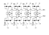
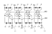
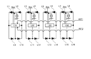
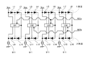
- the light emitting diodes LED1, LED2 and the light emitting diodes LED3, LED4 are turned on at different timings by making the generation timing of the pulse of the first reset signal RST1 different from the generation timing of the pulse of the second reset signal RST2. Can be made. Therefore, as shown in FIG. 7, only two of the four light emitting diodes driven by each LED driver are arranged on the source driver 300 side (hereinafter referred to as “one side”) when viewed from each LED driver. The remaining two are arranged on the opposite side to the source driver 300 (hereinafter referred to as “other side”) when viewed from each LED driver, and the pulse generation timing of the second reset signal RST2 is set to the first timing.
- the light emitting diodes (second light emitting diode group) arranged on the other side are delayed from the light emitting diodes (first light emitting diode group) arranged on the one side. Lights at the timing.
- the light emitting diodes are turned on in the order shown in FIG. That is, the light emitting diodes L1 to L8 are turned on first, then the light emitting diodes L9 to L16 are turned on, then the light emitting diodes L17 to L24 are turned on, and so on. To do. For this reason, the deterioration of the display quality at the time of the moving image display which was produced when the conventional LED driver was employ
- each light emitting diode set as shown in FIG. 7 that is, by arranging a plurality of light emitting diodes included in each light emitting diode set in two rows on the back surface of the display unit 500, As for the light emitting diode, the distance from the LED driver is relatively short.
- the light-emitting diodes are turned on one by one as described above, the occurrence of abnormal lighting due to a voltage drop between the light-emitting diode and the LED driver is suppressed without causing deterioration in display quality when displaying moving images.
- the electric power originally supplied for the light emitting diodes LED1 to LED3 is consumed by the constant current source 111. That is, wasteful power consumption occurs.
- the target luminance values (luminance data) of the light emitting diodes LED1 to LED4 are close to each other, the period during which all of the bypass switches SW1 to SW4 are turned on becomes longer, and the period in which the current flow is stopped. Since it becomes long, wasteful consumption of electric power is suppressed.
- luminance data of the light emitting diode is determined based on image data.
- the luminance data of the light-emitting diode is based on the calculation of a plurality of image data, and the contrast between the distant areas is usually higher when the contrast between the close areas and the contrast between the distant areas are compared. In other words, the brightness data is usually close to each other between close areas.
- the shorter the distance between the light emitting diodes the longer the period during which the current flow is stopped, and the power consumption is effectively reduced.
- FIG. 9 is a block diagram showing the configuration of the PWM control circuit 101 included in the LED driver 100 and its peripheral part in the present embodiment. Hereinafter, differences from the first embodiment will be described.
- the first count value CNT1 is given to the comparators CMP1 and CMP2, and the second count value CNT2 is given to the comparators CMP3 and CMP4.
- a counter selection circuit 105 is provided in the PWM control circuit 101, and each of the comparators CMP1 to CMP4 has a count value selected by the counter selection circuit 105 (first count value CNT1 or second count).
- the value CNT2 is provided.
- the counter selection circuit 105 receives the first count value CNT1, the second count value CNT2, and 2-bit selection data (instruction data) SB output from the shift register 102 for selecting the count value, and receives each comparator CMP1.
- the selection instruction data SB may be set in the counter selection circuit 105 before the register data value RD1 is set in the register REG1, or the shift register is set to 50 bits. Two-bit data may be given to the counter selection circuit 105 as selection instruction data SB.
- FIG. 10 is a block diagram showing a detailed configuration of the counter selection circuit 105.
- the counter selection circuit 105 includes a counter instruction unit 151 and three multiplexers 152 to 154.
- the counter instruction unit 151 receives 2-bit selection data SB (each bit is indicated by “Sbit1” and “Sbit2”), and outputs three selection instruction data SEL2 to SEL4.
- the selection instruction data SEL2 to SEL4 are all 1-bit data.
- the multiplexer 152 supplies either the first count value CNT1 or the second count value CNT2 to the comparator CMP2 based on the selection instruction data SEL2.
- the multiplexer 153 supplies either the first count value CNT1 or the second count value CNT2 to the comparator CMP3 based on the selection instruction data SEL3.
- the multiplexer 154 supplies either the first count value CNT1 or the second count value CNT2 to the comparator CMP4 based on the selection instruction data SEL4.
- the comparator CMP1 is supplied with the first count value CNT1 regardless of the value of the selection data SB.
- the counter instruction unit 151 determines the values of the selection instruction data SEL2 to SEL4 as shown in FIG. For example, when Sbit1 is “1” and Sbit2 is “0”, the selection instruction data SEL2 is “1”, the selection instruction data SEL3 is “0”, and the selection instruction data SEL4 is “0”.
- Each of the multiplexers 152 to 154 provides the first count value CNT1 to the comparators CMP2 to CMP4 if the value of the given selection instruction data SEL2 to SEL4 is “1”, and the given selection instruction data SEL2 to SEL4. Is equal to “0”, the second count value CNT2 is supplied to the comparators CMP2 to CMP4.
- a count value (first count value CNT1 or second count value CNT2) is given to each of the comparators CMP1 to CMP4 according to the value of the selection data SB as shown in FIG. For example, when Sbit1 is “0” and Sbit2 is “1”, the comparators CMP1 and CMP3 are given the first count value CNT1, and the comparators CMP2 and CMP4 are given the second count value CNT2. .
- the count value (first count value CNT1 or second count value CNT2) given to the comparators CMP2 to CMP4 is determined based on the selection data SB. Therefore, by setting the value of the selection data SB in consideration of the arrangement of the respective light emitting diodes LED1 to LED4 (positional relationship between the light emitting diodes LED1 to LED4 and the LED driver 100), the respective light emitting diodes LED1 to LED4 are set. It can be lit at a suitable timing.
- the lighting timing of the light emitting diodes arranged in the second row is more than the lighting timing of the light emitting diodes arranged in the first row.
- each light emitting diode set is arranged as shown in FIG. 7, Sbit1 is set to “1”, Sbit2 is set to “0”, and the pulse generation timing of the second reset signal RST2 is set to the first reset.
- the lighting timing of the light emitting diodes arranged on the other side can be delayed from the lighting timing of the light emitting diodes arranged on the one side.
- Sbit1 is set to “1”
- Sbit2 is set to “0”
- the pulse generation timing of the second reset signal RST2 is set to the first reset.
- the lighting timing of the light emitting diodes arranged on the other side can be delayed from the lighting timing of the light emitting diodes arranged on the one side.
- each light emitting diode set is arranged as shown in FIG. 14, Sbit1 is set to “1”, Sbit2 is set to “1”, and the pulse generation timing of the second reset signal RST2 is set to the first reset. By delaying the generation timing of the pulse of the signal RST1, the lighting timing of the light emitting diodes arranged on the other side can be delayed from the lighting timing of the light emitting diodes arranged on the one side. Furthermore, when each light emitting diode group is arranged as shown in FIG. 15, by setting Sbit1 to “0” and Sbit2 to “0”, all the light emitting diodes included in each light emitting diode group are the same. It can be lit at the timing.
- the degree of freedom in the positional relationship between the light emitting diode and the LED driver is increased, and the display quality is deteriorated at the time of moving image display and the voltage drop between the light emitting diode and the LED driver is caused.
- an LED driver that can suppress the occurrence of abnormal lighting is realized.
- FIG. 16 is a block diagram showing the configuration of the PWM control circuit 101 included in the LED driver 100 and its peripheral part in the present embodiment.
- a delay control register 106 and a comparator 107 are provided in addition to the components in the second embodiment.
- the delay control register 106 stores 12-bit data based on the timing at which the second count value CNT2 should be reset with reference to the reset timing of the first count value CNT1. For example, when the reset timing of the second count value CNT2 should be delayed by a period corresponding to 8 clocks of the PWM control circuit clock signal PCLK rather than the reset timing of the first count value CNT1, the delay control register 106 12-bit data “0000 — 0000 — 1000” is stored.
- the comparator 107 compares the first count value CNT1 with the data value (hereinafter referred to as “delay register value”) DRD stored in the delay control register 106, and indicates whether or not they match.
- the signal is output as a second reset signal RST2 for resetting the second count value CNT2. If the first count value CNT1 matches the delay register value DRD, the comparator 107 sets the logic level of the second reset signal RST2 to the high level, and the first count value CNT1 and the delay register value DRD are equal. If not, the logic level of the second reset signal RST2 is set to a low level.
- the second counter C2 is configured to reset the second count value CNT2 if the logic level of the second reset signal RST2 is high.
- a delay control value holding unit is realized by the delay control register 106
- a delay control value is realized by the delay register value DRD
- a timing control signal generating unit is realized by the comparator 107.
- the second count value CNT2 is reset based on the delay register value DRD stored in advance in the delay control register 106 after the first count value CNT1 is reset.
- the count values (first count value CNT1 or second count value CNT2) to be respectively given to the comparators CMP1 to CMP4 are determined based on the selection data SB. Is done.
- the comparators CMP1 to CMP4 compare the corresponding register data values RD1 to RD4 with the count value (first count value CNT1 or second count value) selected by the counter selection circuit 105, respectively, and whether or not they match. Comparison result signals CS1 to CS4 indicating these are output.
- the switch control circuits SC1 to SC4 control the on / off states of the corresponding bypass switches SW1 to SW4, respectively.
- the LED driver 100 is supplied with two signals, the first reset signal RST1 and the second reset signal RST2, as timing control signals.
- the first reset signal RST1 is supplied to the LED driver 100, while the second reset signal RST2 is generated inside the LED driver 100.
- the degree of freedom in the positional relationship between the light emitting diode and the LED driver is increased, and the display quality at the time of moving image display is increased.
- an LED driver that can suppress the occurrence of abnormal lighting due to a decrease in voltage and a voltage drop between the light emitting diode and the LED driver is realized.
- the configuration shown in FIG. 7 in the first embodiment is the configuration shown in FIG. 17 in the present embodiment. That is, in this embodiment, compared with the first embodiment, the reset signal given from the outside to each LED driver is reduced.
- DESCRIPTION OF SYMBOLS 10 ... LED backlight apparatus 100 ... LED driver 101 ... PWM control circuit 102 ... Shift register 103 ... Constant current drive circuit 104 ... Serial parallel conversion circuit 105 ... Counter selection circuit 110 ... Light emission part 111 ... Constant current source 200 ... Display control circuit 300 ... Source driver (video signal line drive circuit) 400: Gate driver (scanning signal line driving circuit) 500: Display section C1: First counter C2: Second counter CMP1-4: Comparator LED1-4: Light emitting diode (LED) REG1 to 4 ... Register SW1 to 4 ... Switch control circuit
Landscapes
- Engineering & Computer Science (AREA)
- Physics & Mathematics (AREA)
- Computer Hardware Design (AREA)
- General Physics & Mathematics (AREA)
- Theoretical Computer Science (AREA)
- Control Of Indicators Other Than Cathode Ray Tubes (AREA)
- Circuit Arrangement For Electric Light Sources In General (AREA)
- Liquid Crystal (AREA)
Abstract
Description
前記複数の発光ダイオードの各々に或いは所定数毎に並列に接続された複数のスイッチと、
各発光ダイオードに並列に接続されたスイッチのオン/オフ状態を当該各発光ダイオードの目標輝度に応じて切り換えるためのPWM信号を生成するPWM信号生成部と
を備え、
前記PWM信号生成部は、前記複数のスイッチを初期状態としてオン状態またはオフ状態の一方の状態にするタイミングを制御するための複数のタイミング制御信号に基づいて前記PWM信号を生成することを特徴とする。
前記PWM信号生成部は、
前記複数のスイッチにそれぞれ対応して設けられ、各スイッチに対応する発光ダイオードの目標輝度に応じた値であって外部から与えられるクロック信号のパルス数と対応づけられる値である輝度対応値を保持する複数の輝度対応値保持部と、
前記複数のタイミング制御信号がそれぞれ与えられるように設けられ、前記クロック信号のパルス数をカウントしてカウント値として出力する複数のカウンタと、
前記複数のスイッチにそれぞれ対応して設けられ、各スイッチに対応する輝度対応値保持部に保持されている輝度対応値と前記複数のカウンタのうちのいずれかのカウンタから出力されるカウント値とを比較し、それらが一致した時に当該各スイッチのオン/オフ状態を前記初期状態から切り換える複数のスイッチ切換部と
を含み、
各スイッチは、当該各スイッチに対応するスイッチ切換部によって比較されるカウント値を出力するカウンタに与えられるタイミング制御信号に基づいて初期状態にされ、
各カウンタから出力されるカウント値は、当該各カウンタに与えられるタイミング制御信号に基づいてリセットされることを特徴とする。
各スイッチ切換部によって比較されるカウント値を出力するカウンタが予め定められていることを特徴とする。
前記PWM信号生成部は、各スイッチ切換部によって比較されるべきカウント値を出力するカウンタを所定の指示データに基づいて選択するカウンタ選択部を更に含むことを特徴とする。
前記複数のカウンタは、外部からタイミング制御信号を受け取る第1のカウンタと該第1のカウンタ以外の第2のカウンタとからなり、
前記PWM信号生成部は、
前記複数のスイッチについての初期状態にされるタイミングの差に応じた値であって前記クロック信号のパルス数と対応づけられる値である遅延制御値を保持する遅延制御値保持部と、
前記第2のカウンタに対応して設けられ、前記遅延制御値保持部に保持されている遅延制御値と前記第1のカウンタから出力されるカウント値とに基づいて、前記第2のカウンタに与えるためのタイミング制御信号を生成するタイミング制御信号生成部と
を更に含み、
前記タイミング制御信号生成部は、前記遅延制御値保持部に保持されている遅延制御値と前記第1のカウンタから出力されるカウント値とが一致した時に、前記第2のカウンタから出力されるカウント値がリセットされるように、前記タイミング制御信号を生成することを特徴とする。
前記複数のスイッチの全てがオン状態になったときに前記定電流源に流れる電流を零にする定電流駆動部を更に備えることを特徴とする。
前記面状照明装置は複数の発光ダイオード駆動回路を有し、
各発光ダイオード駆動回路によって駆動される複数の発光ダイオードには、当該各発光ダイオード駆動回路の配置位置を基準として一側に配置される発光ダイオードである第1の発光ダイオード群と当該各発光ダイオード駆動回路の配置位置を基準として他側に配置される発光ダイオードである第2の発光ダイオード群とが含まれ、
前記第1の発光ダイオード群に並列に接続されたスイッチと前記第2の発光ダイオード群に並列に接続されたスイッチとは、異なるタイミング制御信号に基づいて前記初期状態にされることを特徴とする。
<1.1 全体構成および動作の概要>
図2は、本発明の第1の実施形態に係るLEDバックライト装置(面状照明装置)10を備えた液晶表示装置の全体構成を示すブロック図である。この液晶表示装置は、LEDバックライト装置10と、表示制御回路200と、ソースドライバ(映像信号線駆動回路)300と、ゲートドライバ(走査信号線駆動回路)400と、表示部500とを備えている。LEDバックライト装置10には、表示部500の背面から(当該表示部500に)光を照射するためのバックライトを構成する複数の発光ダイオードからなる発光部110と、発光部110内の発光ダイオードを駆動するLEDドライバ100とが含まれている。なお、この液晶表示装置においては、表示部500は複数のエリアに分割され、各エリアの入力画像に基づき発光ダイオードの輝度を制御しながら表示部500を駆動するエリアアクティブ駆動が行われる。
図5は、本実施形態におけるLEDドライバ100の概略構成図である。なお、LEDドライバ100は複数個の発光ダイオードからなる発光ダイオード組毎に設けられる(すなわち、1個のLEDドライバ100は複数個の発光ダイオードを駆動する)ところ、以下においては、4個の発光ダイオードにつき1個のLEDドライバ100が設けられる例を挙げて説明する。
次に、本実施形態において発光ダイオードの輝度の制御が具体的にどのようにして行われるかについて説明する。本実施形態においては、第1のカウンタC1および第2のカウンタC2は12ビットで構成され、各バイパススイッチSW1~SW4に対応して設けられているレジスタREG1~REG4についても12ビットで構成されている。また、バイパススイッチSW1~SW4については、第1カウント値CNT1または第2カウント値CNT2とレジスタデータ値RD1~RD4との比較結果に基づいてオン/オフ状態の制御が行われる。従って、本実施形態に係るLEDドライバ100では(PWM制御回路用クロック信号PCLKの)4096クロックを1周期としてPWM制御が行われる。各バイパススイッチSW1~SW4は、対応するカウンタの値がリセットされるとオフ状態にされ、対応するカウンタの値と対応するレジスタの値とが一致するとオン状態にされる。これにより、各発光ダイオードLED1~LED4は(PWM制御の)1周期のうちの所望の期間(目標輝度に応じた期間)だけ点灯状態となる。
本実施形態によれば、4個の発光ダイオードLED1~LED4につき1個のLEDドライバ100が設けられ、各発光ダイオードLED1~LED4にそれぞれ並列にバイパススイッチSW1~SW4が設けられている。ここで、バイパススイッチSW1,SW2については、第1のリセット信号RST1のパルスの発生タイミングで初期状態としてのオフ状態にされ、発光ダイオードLED1,LED2の目標輝度に応じた期間だけ当該オフ状態が維持される。一方、バイパススイッチSW3,SW4については、第2のリセット信号RST2のパルスの発生タイミングで初期状態としてのオフ状態にされ、発光ダイオードLED3,LED4の目標輝度に応じた期間だけ当該オフ状態が維持される。このため、第1のリセット信号RST1のパルスの発生タイミングと第2のリセット信号RST2のパルスの発生タイミングとを異ならせることにより、発光ダイオードLED1,LED2と発光ダイオードLED3,LED4とを異なるタイミングで点灯させることができる。従って、図7に示すように、各LEDドライバが駆動する4個の発光ダイオードのうちの2個だけを当該各LEDドライバからみてソースドライバ300側(以下、「一側」という。)に配置し、残りの2個を当該各LEDドライバからみてソースドライバ300とは反対側(以下、「他側」という。)に配置する構成とし、第2のリセット信号RST2のパルスの発生タイミングを第1のリセット信号RST1のパルスの発生タイミングよりも遅らせることによって、他側に配置された発光ダイオード(第2の発光ダイオード群)は一側に配置された発光ダイオード(第1の発光ダイオード群)よりも遅れたタイミングで点灯する。このようにして、発光部110では、図8に示す順序で発光ダイオードの点灯が行われる。すなわち、「まず発光ダイオードL1~L8が点灯し、次に発光ダイオードL9~L16が点灯し、次に発光ダイオードL17~L24が点灯し、・・・」というように、1列ずつ発光ダイオードが点灯する。このため、従来のLEDドライバを採用したときに生じていた動画表示の際の表示品位の低下が防止される。
<2.1 構成および動作>
次に、本発明の第2の実施形態について説明する。本実施形態における液晶表示装置の全体構成およびLEDドライバ100の概略構成については上記第1の実施形態と同様であるので、説明を省略する(図2および図5参照)。図9は、本実施形態において、LEDドライバ100に含まれるPWM制御回路101およびその周辺部の構成を示すブロック図である。以下、上記第1の実施形態と異なる点について説明する。
本実施形態によれば、比較器CMP2~CMP4に与えられるカウント値(第1カウント値CNT1または第2カウント値CNT2)は、選択用データSBに基づいて決定される。このため、各発光ダイオードLED1~LED4の配置(発光ダイオードLED1~LED4とLEDドライバ100との位置関係)を考慮して選択用データSBの値を設定することにより、当該各発光ダイオードLED1~LED4を好適なタイミングで点灯させることができる。これにより、例えば、発光ダイオードLED1~LED4が2列で配置されているときに、2列目に配置されている発光ダイオードの点灯タイミングを1列目に配置されている発光ダイオードの点灯タイミングよりも遅らせることによって、動画表示の際の表示品位が低下が防止される。
<3.1 構成および動作>
次に、本発明の第3の実施形態について説明する。本実施形態における液晶表示装置の全体構成およびLEDドライバ100の概略構成については上記第1および第2の実施形態と同様であるので、説明を省略する(図2および図5参照)。但し、上記第1および第2の実施形態においては、2つのリセット信号(第1のリセット信号RST1および第2のリセット信号RST2)がLEDドライバ100に与えられていたが、本実施形態においては、第1のリセット信号RST1のみがLEDドライバ100に(LEDドライバ100の外部から)与えられる。図16は、本実施形態において、LEDドライバ100に含まれるPWM制御回路101およびその周辺部の構成を示すブロック図である。以下、上記第2の実施形態と異なる点について説明する。
上記第1および第2の実施形態においては、LEDドライバ100にはタイミング制御信号として第1のリセット信号RST1および第2のリセット信号RST2の2つの信号が与えられていたが、本実施形態においては、第1のリセット信号RST1についてはLEDドライバ100に与えられるが、第2のリセット信号RST2についてはLEDドライバ100の内部で生成される。このため、LEDドライバ100に与える外部入力信号を削減しつつ、上記第2の実施形態と同様に、発光ダイオードとLEDドライバとの位置関係についての自由度を高めつつ、動画表示の際の表示品位の低下や発光ダイオード-LEDドライバ間の電圧降下に起因する点灯異常の発生を抑制することのできるLEDドライバが実現される。
100…LEDドライバ
101…PWM制御回路
102…シフトレジスタ
103…定電流駆動回路
104…シリアルパラレル変換回路
105…カウンタ選択回路
110…発光部
111…定電流源
200…表示制御回路
300…ソースドライバ(映像信号線駆動回路)
400…ゲートドライバ(走査信号線駆動回路)
500…表示部
C1…第1のカウンタ
C2…第2のカウンタ
CMP1~4…比較器
LED1~4…発光ダイオード(LED)
REG1~4…レジスタ
SW1~4…スイッチ制御回路
Claims (8)
- 互いに直列に接続され、かつ、一定の電流を流すための定電流源に直列に接続された複数の発光ダイオードを駆動する発光ダイオード駆動回路であって、
前記複数の発光ダイオードの各々に或いは所定数毎に並列に接続された複数のスイッチと、
各発光ダイオードに並列に接続されたスイッチのオン/オフ状態を当該各発光ダイオードの目標輝度に応じて切り換えるためのPWM信号を生成するPWM信号生成部と
を備え、
前記PWM信号生成部は、前記複数のスイッチを初期状態としてオン状態またはオフ状態の一方の状態にするタイミングを制御するための複数のタイミング制御信号に基づいて前記PWM信号を生成することを特徴とする、発光ダイオード駆動回路。 - 前記PWM信号生成部は、
前記複数のスイッチにそれぞれ対応して設けられ、各スイッチに対応する発光ダイオードの目標輝度に応じた値であって外部から与えられるクロック信号のパルス数と対応づけられる値である輝度対応値を保持する複数の輝度対応値保持部と、
前記複数のタイミング制御信号がそれぞれ与えられるように設けられ、前記クロック信号のパルス数をカウントしてカウント値として出力する複数のカウンタと、
前記複数のスイッチにそれぞれ対応して設けられ、各スイッチに対応する輝度対応値保持部に保持されている輝度対応値と前記複数のカウンタのうちのいずれかのカウンタから出力されるカウント値とを比較し、それらが一致した時に当該各スイッチのオン/オフ状態を前記初期状態から切り換える複数のスイッチ切換部と
を含み、
各スイッチは、当該各スイッチに対応するスイッチ切換部によって比較されるカウント値を出力するカウンタに与えられるタイミング制御信号に基づいて初期状態にされ、
各カウンタから出力されるカウント値は、当該各カウンタに与えられるタイミング制御信号に基づいてリセットされることを特徴とする、請求項1に記載の発光ダイオード駆動回路。 - 各スイッチ切換部によって比較されるカウント値を出力するカウンタが予め定められていることを特徴とする、請求項2に記載の発光ダイオード駆動回路。
- 前記PWM信号生成部は、各スイッチ切換部によって比較されるべきカウント値を出力するカウンタを所定の指示データに基づいて選択するカウンタ選択部を更に含むことを特徴とする、請求項2に記載の発光ダイオード駆動回路。
- 前記複数のカウンタは、外部からタイミング制御信号を受け取る第1のカウンタと該第1のカウンタ以外の第2のカウンタとからなり、
前記PWM信号生成部は、
前記複数のスイッチについての初期状態にされるタイミングの差に応じた値であって前記クロック信号のパルス数と対応づけられる値である遅延制御値を保持する遅延制御値保持部と、
前記第2のカウンタに対応して設けられ、前記遅延制御値保持部に保持されている遅延制御値と前記第1のカウンタから出力されるカウント値とに基づいて、前記第2のカウンタに与えるためのタイミング制御信号を生成するタイミング制御信号生成部と
を更に含み、
前記タイミング制御信号生成部は、前記遅延制御値保持部に保持されている遅延制御値と前記第1のカウンタから出力されるカウント値とが一致した時に、前記第2のカウンタから出力されるカウント値がリセットされるように、前記タイミング制御信号を生成することを特徴とする、請求項2に記載の発光ダイオード駆動回路。 - 前記複数のスイッチの全てがオン状態になったときに前記定電流源に流れる電流を零にする定電流駆動部を更に備えることを特徴とする、請求項1に記載の発光ダイオード駆動回路。
- 請求項1から6までのいずれか1項に記載の発光ダイオード駆動回路を備えたことを特徴とする面状照明装置。
- 前記面状照明装置は複数の発光ダイオード駆動回路を有し、
各発光ダイオード駆動回路によって駆動される複数の発光ダイオードには、当該各発光ダイオード駆動回路の配置位置を基準として一側に配置される発光ダイオードである第1の発光ダイオード群と当該各発光ダイオード駆動回路の配置位置を基準として他側に配置される発光ダイオードである第2の発光ダイオード群とが含まれ、
前記第1の発光ダイオード群に並列に接続されたスイッチと前記第2の発光ダイオード群に並列に接続されたスイッチとは、異なるタイミング制御信号に基づいて前記初期状態にされることを特徴とする、請求項7に記載の面状照明装置。
Priority Applications (2)
| Application Number | Priority Date | Filing Date | Title |
|---|---|---|---|
| CN2009801464829A CN102224606A (zh) | 2009-01-09 | 2009-08-28 | 发光二极管驱动电路和具备该发光二极管驱动电路的面状照明装置 |
| US12/998,483 US20110199011A1 (en) | 2009-01-09 | 2009-08-28 | Light-emitting diode driving circuit and planar illuminating device having same |
Applications Claiming Priority (2)
| Application Number | Priority Date | Filing Date | Title |
|---|---|---|---|
| JP2009-003497 | 2009-01-09 | ||
| JP2009003497 | 2009-01-09 |
Publications (1)
| Publication Number | Publication Date |
|---|---|
| WO2010079635A1 true WO2010079635A1 (ja) | 2010-07-15 |
Family
ID=42316410
Family Applications (1)
| Application Number | Title | Priority Date | Filing Date |
|---|---|---|---|
| PCT/JP2009/065091 Ceased WO2010079635A1 (ja) | 2009-01-09 | 2009-08-28 | 発光ダイオード駆動回路およびそれを備えた面状照明装置 |
Country Status (3)
| Country | Link |
|---|---|
| US (1) | US20110199011A1 (ja) |
| CN (1) | CN102224606A (ja) |
| WO (1) | WO2010079635A1 (ja) |
Cited By (2)
| Publication number | Priority date | Publication date | Assignee | Title |
|---|---|---|---|---|
| CN102737583A (zh) * | 2012-07-09 | 2012-10-17 | 深圳市磊芯半导体有限公司 | Led驱动恒流通道输出驱动器、级联系统及其驱动方法 |
| JP2016503587A (ja) * | 2012-11-21 | 2016-02-04 | オスラム オプト セミコンダクターズ ゲゼルシャフト ミット ベシュレンクテル ハフツングOsram Opto Semiconductors GmbH | 光電半導体部品 |
Families Citing this family (27)
| Publication number | Priority date | Publication date | Assignee | Title |
|---|---|---|---|---|
| TWI437920B (zh) * | 2011-08-08 | 2014-05-11 | Weltrend Semiconductor Inc | 利用電源開關選擇光源發光模式之光源控制器及其照明系統 |
| EP2661153B1 (en) * | 2012-05-02 | 2019-11-06 | ams AG | Current source and method for providing a driving current |
| CN103079314B (zh) * | 2012-12-28 | 2015-05-20 | 电子科技大学 | 多路电流源切换装置 |
| EP3207602B1 (en) | 2014-10-15 | 2025-09-03 | Lumentum Operations LLC | Laser system and method of tuning the output power of the laser system |
| US9640108B2 (en) | 2015-08-25 | 2017-05-02 | X-Celeprint Limited | Bit-plane pulse width modulated digital display system |
| US9814105B2 (en) * | 2015-11-12 | 2017-11-07 | Semiconductor Components Industries, Llc | Control circuit for LED and active bleeder thereof |
| US10091446B2 (en) | 2015-12-23 | 2018-10-02 | X-Celeprint Limited | Active-matrix displays with common pixel control |
| US9930277B2 (en) | 2015-12-23 | 2018-03-27 | X-Celeprint Limited | Serial row-select matrix-addressed system |
| US9928771B2 (en) | 2015-12-24 | 2018-03-27 | X-Celeprint Limited | Distributed pulse width modulation control |
| US10360846B2 (en) | 2016-05-10 | 2019-07-23 | X-Celeprint Limited | Distributed pulse-width modulation system with multi-bit digital storage and output device |
| US10453826B2 (en) | 2016-06-03 | 2019-10-22 | X-Celeprint Limited | Voltage-balanced serial iLED pixel and display |
| CN109691235B (zh) * | 2016-09-09 | 2021-02-19 | 株式会社小糸制作所 | 点亮电路、车辆用灯具及光源的驱动方法 |
| US10832609B2 (en) | 2017-01-10 | 2020-11-10 | X Display Company Technology Limited | Digital-drive pulse-width-modulated output system |
| US10201049B1 (en) * | 2017-08-03 | 2019-02-05 | Apple Inc. | Local display backlighting systems and methods |
| US10426010B2 (en) | 2017-12-29 | 2019-09-24 | Texas Instruments Incorporated | LED driver |
| US10368412B2 (en) * | 2017-12-29 | 2019-07-30 | Texas Instruments Incorporated | LED driver |
| US10885830B2 (en) * | 2018-07-24 | 2021-01-05 | Innolux Corporation | Electronic device capable of reducing color shift |
| DE102018118876A1 (de) * | 2018-08-03 | 2020-02-06 | HELLA GmbH & Co. KGaA | Verfahren und Mittel zum Einstellen einer Stromquelle für ein Leuchtdiodenfeld |
| US10455653B1 (en) * | 2018-08-09 | 2019-10-22 | Innolux Corporation | LED driving circuits |
| KR102591274B1 (ko) * | 2019-02-13 | 2023-10-20 | 삼성디스플레이 주식회사 | 광원 장치 및 이를 포함하는 표시 장치 |
| US12142716B2 (en) | 2019-03-29 | 2024-11-12 | Creeled, Inc. | Active control of light emitting diodes and light emitting diode displays |
| CN115917631A (zh) * | 2020-03-11 | 2023-04-04 | 科锐Led公司 | 发光二极管和发光二极管显示器的有源控制 |
| US11197359B1 (en) * | 2020-07-14 | 2021-12-07 | Himax Technologies Limited | Backlight module and display apparatus |
| CN112911757A (zh) * | 2021-01-27 | 2021-06-04 | 上汽大众汽车有限公司 | 多功能led驱动系统和驱动方法 |
| CN113141691A (zh) * | 2021-04-30 | 2021-07-20 | 上汽大众汽车有限公司 | 一种流水式位置灯的驱动控制装置 |
| CN116458148A (zh) * | 2021-11-05 | 2023-07-18 | 京东方科技集团股份有限公司 | 用于生成驱动信号的方法和设备、背光源和显示设备 |
| CN114554647B (zh) * | 2022-03-16 | 2023-07-25 | 无锡英迪芯微电子科技股份有限公司 | 适用于矩阵式led大灯驱动的pwm产生方法及电路 |
Citations (5)
| Publication number | Priority date | Publication date | Assignee | Title |
|---|---|---|---|---|
| JP2003264316A (ja) * | 2002-03-11 | 2003-09-19 | Fuji Electric Co Ltd | Led制御回路 |
| JP2006164842A (ja) * | 2004-12-09 | 2006-06-22 | Nec Lcd Technologies Ltd | 照明装置、液晶表示装置,携帯端末装置およびその制御方法 |
| JP2006210435A (ja) * | 2005-01-25 | 2006-08-10 | Rohm Co Ltd | 電源装置、発光装置ならびに表示装置 |
| JP2007066897A (ja) * | 2005-08-26 | 2007-03-15 | Philips Lumileds Lightng Co Llc | 統合された電子機器を用いたバックライティングのためのled光源 |
| JP2008171983A (ja) * | 2007-01-11 | 2008-07-24 | Seiko Epson Corp | 光源装置、画像表示装置、プロジェクタおよび光源制御方法 |
Family Cites Families (5)
| Publication number | Priority date | Publication date | Assignee | Title |
|---|---|---|---|---|
| JP3229250B2 (ja) * | 1997-09-12 | 2001-11-19 | インターナショナル・ビジネス・マシーンズ・コーポレーション | 液晶表示装置における画像表示方法及び液晶表示装置 |
| JP4123183B2 (ja) * | 2004-04-20 | 2008-07-23 | ソニー株式会社 | 定電流駆動装置、バックライト光源装置及びカラー液晶表示装置 |
| JP4400401B2 (ja) * | 2004-09-30 | 2010-01-20 | セイコーエプソン株式会社 | 電気光学装置とその駆動方法及び電子機器 |
| WO2007054856A2 (en) * | 2005-11-08 | 2007-05-18 | Koninklijke Philips Electronics N.V. | Circuit arrangement and method of driving a circuit arrangement |
| CN102124573A (zh) * | 2008-10-01 | 2011-07-13 | 夏普株式会社 | 面状照明装置和具备它的显示装置 |
-
2009
- 2009-08-28 WO PCT/JP2009/065091 patent/WO2010079635A1/ja not_active Ceased
- 2009-08-28 CN CN2009801464829A patent/CN102224606A/zh active Pending
- 2009-08-28 US US12/998,483 patent/US20110199011A1/en not_active Abandoned
Patent Citations (5)
| Publication number | Priority date | Publication date | Assignee | Title |
|---|---|---|---|---|
| JP2003264316A (ja) * | 2002-03-11 | 2003-09-19 | Fuji Electric Co Ltd | Led制御回路 |
| JP2006164842A (ja) * | 2004-12-09 | 2006-06-22 | Nec Lcd Technologies Ltd | 照明装置、液晶表示装置,携帯端末装置およびその制御方法 |
| JP2006210435A (ja) * | 2005-01-25 | 2006-08-10 | Rohm Co Ltd | 電源装置、発光装置ならびに表示装置 |
| JP2007066897A (ja) * | 2005-08-26 | 2007-03-15 | Philips Lumileds Lightng Co Llc | 統合された電子機器を用いたバックライティングのためのled光源 |
| JP2008171983A (ja) * | 2007-01-11 | 2008-07-24 | Seiko Epson Corp | 光源装置、画像表示装置、プロジェクタおよび光源制御方法 |
Cited By (4)
| Publication number | Priority date | Publication date | Assignee | Title |
|---|---|---|---|---|
| CN102737583A (zh) * | 2012-07-09 | 2012-10-17 | 深圳市磊芯半导体有限公司 | Led驱动恒流通道输出驱动器、级联系统及其驱动方法 |
| JP2016503587A (ja) * | 2012-11-21 | 2016-02-04 | オスラム オプト セミコンダクターズ ゲゼルシャフト ミット ベシュレンクテル ハフツングOsram Opto Semiconductors GmbH | 光電半導体部品 |
| US9871075B2 (en) | 2012-11-21 | 2018-01-16 | Osram Opto Semiconductors Gmbh | Optoelectronic semiconductor component |
| US9997559B2 (en) | 2012-11-21 | 2018-06-12 | Osram Opto Semiconductors Gmbh | Optoelectronic semiconductor component |
Also Published As
| Publication number | Publication date |
|---|---|
| CN102224606A (zh) | 2011-10-19 |
| US20110199011A1 (en) | 2011-08-18 |
Similar Documents
| Publication | Publication Date | Title |
|---|---|---|
| WO2010079635A1 (ja) | 発光ダイオード駆動回路およびそれを備えた面状照明装置 | |
| US8963810B2 (en) | LED display systems | |
| KR101329967B1 (ko) | 백 라이트 유닛과 이를 이용한 액정 표시장치 및 그의 구동방법 | |
| JP2020027273A (ja) | バックライト装置およびそれを備える表示装置 | |
| TWI900695B (zh) | 具有像素電路的顯示器系統及像素驅動電路 | |
| US11626062B2 (en) | System and method for modulating an array of emissive elements | |
| EP2128687A1 (en) | Light source device and liquid crystal display device | |
| US20220076610A1 (en) | Display using analog and digital subframes | |
| KR20180003402A (ko) | 유기 발광 표시 장치 | |
| US11699387B2 (en) | Display device | |
| KR20100054494A (ko) | 광원 구동 방법, 이를 수행하기 위한 광원 장치 및 이 광원장치를 포함하는 표시 장치 | |
| WO2016084544A1 (ja) | 画素ユニット、表示パネル、および信号伝送方法 | |
| KR20210083946A (ko) | 발광표시장치 및 이의 구동방법 | |
| US10877315B2 (en) | Backlight and display device provided with same | |
| KR20110075158A (ko) | 기준전압 생성회로 | |
| CN110599945B (zh) | Led显示装置及其驱动方法 | |
| KR101877776B1 (ko) | 백라이트 드라이버용 구동집적회로 및 그를 포함하는 액정표시장치 | |
| JP6134701B2 (ja) | Ledアレイ制御のための装置及び方法 | |
| US8674927B2 (en) | Liquid crystal display and method of driving the same | |
| CN103150993A (zh) | Amoled像素阵列驱动装置 | |
| JP5186627B2 (ja) | 表示装置 | |
| JP5901185B2 (ja) | バックライト装置及びその制御方法 | |
| KR101622535B1 (ko) | 발광 다이오드 어레이의 구동 장치 및 구동 방법, 및 이를 이용하는 액정 표시 장치 | |
| KR102219578B1 (ko) | 표시장치 | |
| KR102605058B1 (ko) | 백라이트 유닛 및 이를 포함하는 표시장치 |
Legal Events
| Date | Code | Title | Description |
|---|---|---|---|
| WWE | Wipo information: entry into national phase |
Ref document number: 200980146482.9 Country of ref document: CN |
|
| 121 | Ep: the epo has been informed by wipo that ep was designated in this application |
Ref document number: 09837521 Country of ref document: EP Kind code of ref document: A1 |
|
| WWE | Wipo information: entry into national phase |
Ref document number: 12998483 Country of ref document: US |
|
| NENP | Non-entry into the national phase |
Ref country code: DE |
|
| 122 | Ep: pct application non-entry in european phase |
Ref document number: 09837521 Country of ref document: EP Kind code of ref document: A1 |
|
| NENP | Non-entry into the national phase |
Ref country code: JP |