WO2010074066A1 - 光学素子、光ピックアップ装置及び光学素子の製造方法 - Google Patents
光学素子、光ピックアップ装置及び光学素子の製造方法 Download PDFInfo
- Publication number
- WO2010074066A1 WO2010074066A1 PCT/JP2009/071300 JP2009071300W WO2010074066A1 WO 2010074066 A1 WO2010074066 A1 WO 2010074066A1 JP 2009071300 W JP2009071300 W JP 2009071300W WO 2010074066 A1 WO2010074066 A1 WO 2010074066A1
- Authority
- WO
- WIPO (PCT)
- Prior art keywords
- light
- optical element
- resistant stabilizer
- layer
- plate
- Prior art date
- Legal status (The legal status is an assumption and is not a legal conclusion. Google has not performed a legal analysis and makes no representation as to the accuracy of the status listed.)
- Ceased
Links
Images
Classifications
-
- G—PHYSICS
- G11—INFORMATION STORAGE
- G11B—INFORMATION STORAGE BASED ON RELATIVE MOVEMENT BETWEEN RECORD CARRIER AND TRANSDUCER
- G11B7/00—Recording or reproducing by optical means, e.g. recording using a thermal beam of optical radiation by modifying optical properties or the physical structure, reproducing using an optical beam at lower power by sensing optical properties; Record carriers therefor
- G11B7/12—Heads, e.g. forming of the optical beam spot or modulation of the optical beam
- G11B7/135—Means for guiding the beam from the source to the record carrier or from the record carrier to the detector
- G11B7/1372—Lenses
- G11B7/1374—Objective lenses
-
- G—PHYSICS
- G02—OPTICS
- G02B—OPTICAL ELEMENTS, SYSTEMS OR APPARATUS
- G02B1/00—Optical elements characterised by the material of which they are made; Optical coatings for optical elements
- G02B1/10—Optical coatings produced by application to, or surface treatment of, optical elements
- G02B1/11—Anti-reflection coatings
- G02B1/113—Anti-reflection coatings using inorganic layer materials only
- G02B1/115—Multilayers
Definitions
- the present invention relates to an optical element, an optical pickup device, and an optical element manufacturing method.
- the optical pickup device includes an optical element unit that irradiates a medium with light having a predetermined wavelength emitted from a light source, and receives the reflected light with a light receiving element.
- the optical element unit receives the light from a reflection layer or a light receiving medium of the medium.
- An optical element such as a lens for condensing light by the element is included.
- BD Blu-ray Disc
- a main object of the present invention is to provide an optical element, an optical pickup device, and an optical element manufacturing method capable of suppressing a decrease in light resistance due to irradiation with blue laser light without causing a light-resistant stabilizer bleed out. It is to provide.
- an optical pickup device using the optical element as an objective lens, A light source that emits laser light having a wavelength of 380 nm to 420 nm; The objective lens receiving the laser beam; An optical pickup device is provided.
- the deterioration of the optical element due to the blue laser beam is particularly caused at the interface between the molding part and the air layer as the base material of the optical element or the interface between the molding part and the functional layer such as the antireflection layer. It occurred remarkably and it became clear that the problem was small inside the molded part. Therefore, according to the present invention, by forming a light-resistant stabilizer layer on the surface of the molded part, it becomes possible to localize the light-resistant stabilizer on the surface of the molded part, and even when irradiated with laser light, It is possible to suppress the deterioration of the resin on the surface of the molded part, which is particularly problematic.
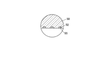
- FIG. 5 is a schematic enlarged cross-sectional view showing a modification of the surface of the molded part in a preferred embodiment of the present invention, particularly showing a state in which a concave portion is formed on the surface of the molded part and a light-resistant stabilizer layer is filled.
- FIG. 5 is a schematic expanded sectional view which shows the modification of the surface of the shaping
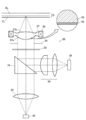
- the optical pickup device 30 is provided with a semiconductor laser oscillator 32.
- the semiconductor laser oscillator 32 is an example of a light source, and emits blue laser light (blue-violet laser) having a specific wavelength (for example, 405 nm) having a wavelength of 380 to 420 nm for BD (Blu-ray Disc).
- a collimator 33, a beam splitter 34, a quarter wavelength plate 35, a diaphragm 36, and an objective lens 37 are arranged in a direction away from the semiconductor laser oscillator 32. Are sequentially arranged.
- a sensor lens group 38 and a sensor 39 made up of two sets of lenses are sequentially arranged in a direction close to the beam splitter 34 and perpendicular to the optical axis of the blue-violet light described above.
- the objective lens 37 is disposed at a position facing the high-density optical disc D (BD optical disc), and condenses the blue laser light emitted from the semiconductor laser oscillator 32 on one surface of the optical disc D. Yes.
- the objective lens 37 has an image-side numerical aperture NA of 0.7 or more.
- the objective lens 37 is an example of an optical element, and the objective lens 37 is provided with a two-dimensional actuator 40. By the operation of the two-dimensional actuator 40, the objective lens 37 is movable on the optical axis.
- the objective lens 37 is mainly composed of a molded part 50, and a light-resistant stabilizer layer 55 is formed on the surface 37a.
- the molding part 50 is molded into a lens shape and exhibits essential optical functions such as a light collecting function.
- An alicyclic olefin resin is used for the molding part 50.
- ZEON ZEONEX
- Mitsui Chemicals APEL
- JSR Arton
- Chicona TOPAS, etc.
- the light-resistant stabilizer layer 55 is a layer containing a light-resistant stabilizer and is a layer having a higher amount of light-resistant stabilizer than the molded part 50. Although it does not specifically limit as a manufacturing method, For example, the layer formed by dipping a shaping
- the layer thickness of the light-resistant stabilizer layer 55 is preferably 10 to 100 ⁇ m.
- the ratio of the polymer matrix resin is not particularly limited, but the ratio of the light stabilizer to the polymer matrix resin is preferably 0.1% by mass to 30% by mass. If the content of the light-resistant stabilizer is small, the effect is low. On the other hand, if the amount is too large, the binder layer cannot be retained and is crumbly. A more preferable content is 5% by mass to 10% by mass.
- a resin similar to a molded product, a photocurable resin composition, or various binder resins can be used.
- a high-molecular-weight light-resistant stabilizer made of a polycondensate or a polymer that itself has a film-forming ability for the light-resistant stabilizer layer.
- a light-resistant stabilizer layer can be formed on the surface of the molded part by dipping in a solution in which a high-molecular weight light-resistant stabilizer comprising a polycondensate or a polymer is dissolved and drying.
- Examples of the light-resistant stabilizer constituting the light-resistant stabilizer layer 55 include a benzophenone-based light-resistant stabilizer, a benzotriazole-based light-resistant stabilizer, a hindered amine-based light-resistant stabilizer, and the like. From the viewpoint of colorability and the like, it is preferable to use a hindered amine light resistance stabilizer (HALS).
- HALS hindered amine light resistance stabilizer
- HALS includes N, N ′, N ′′, N ′ ′′-tetrakis- [4,6-bis- ⁇ butyl- (N-methyl-2,2,6,6-tetramethylpiperidin-4-yl) amino ⁇ -Triazin-2-yl] -4,7-diazadecane-1,10-diamine, dibutylamine and 1,3,5-triazine, N, N'-bis (2,2,6,6-tetramethyl Polycondensate with -4-piperidyl) butylamine, poly [ ⁇ (1,1,3,3-tetramethylbutyl) amino-1,3,5-triazine-2,4-diyl ⁇ ⁇ (2,2, 6,6-tetramethyl-4-piperidyl) imino ⁇ hexamethylene ⁇ (2,2,6,6-tetramethyl-4-piperidyl) imino ⁇ ], 1,6-hexanediamine-N, N′-bis ( 2,2,6,6-tetramethyl
- the addition amount of the light-resistant stabilizer is preferably 1.5% by mass or less, more preferably 1.0% by mass or less, based on the total amount including the resin and the light-resistant stabilizer.
- the same light-resistant stabilizer that constitutes the light-resistant stabilizer layer 55 can be used as the light-resistant stabilizer added to the resin.
- the light-resistant stabilizer added to the resin of the molded part is not limited to the polycondensate or high molecular weight type, but also has a molecular weight of 1,000, such as trade names ADK STAB LA52, LA57, LA62, LA67 manufactured by ADEKA, for example. Less than low molecular weight compounds can be used.
- the light-resistant stabilizer layer 55 may be formed on the surface 37a of the molded part 50 by intentionally forming a large number of recesses 52 in the molded part 50 and filling the light-resistant stabilizer layer 55.
- the recess 52 preferably has a diameter of 100 nm or less and a depth of 1 ⁇ m or less.
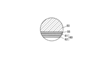
- an antireflection film 60 may be formed on the light-resistant stabilizer layer 55.
- the antireflection film 60 may be a single layer or a plurality of layers, but a structure having two or more layers is preferable in order to enhance the antireflection effect. In that case, after providing the light-resistant stabilizer layer 55 with respect to the shaping
- the first layer 61 is a layer made of a high refractive index material having a refractive index of 1.7 or more, preferably Ta 2 O 5 , a mixture of Ta 2 O 5 and TiO 2 , ZrO 2. , ZrO 2 and a mixture of TiO 2 .
- the first layer 61 may be composed of TiO 2 , Nb 2 O 3 , and HfO 2 .
- the second layer 62 is a layer made of a low refractive index material having a refractive index of less than 1.7, and is preferably made of SiO 2 and MgF 2 .
- the first layer 61 and the second layer 62 may be alternately stacked on the first layer 61 and the second layer 62, and the antireflection film 60 may have a 2-7 layer structure as a whole.
- the layer that is in direct contact with the molded part 50 may be a high refractive index material layer (first layer 61) or a low refractive index material layer (second layer) depending on the type of the molded part 50.
- the layer 62) may be used.
- the layer that is in direct contact with the molded part 50 is a layer of a high refractive index material.
- the light-resistant stabilizer layer 55, the concave portion 52, and the antireflection film are formed on the back surface 37b in the same manner as the light-resistant stabilizer layer 55, the concave portion 52, and the antireflection film 60 are formed on the front surface 37a. 60 may be formed.
- thermoplastic resin is injection-molded into a mold under a certain condition to form a molded part 50 having a predetermined shape.
- a light-resistant stabilizer layer 55 is formed on the surface 37a of the molded part 50.
- the molded part 50 was dipped (immersed) at a constant temperature for a fixed time in a solution (aqueous solution) in which the light-resistant stabilizer was dissolved in a solvent such as water, and adhered to the molded part 50.
- aqueous solution a solution in which the light-resistant stabilizer was dissolved in a solvent such as water
- There are a method of drying the aqueous solution a method of applying the aqueous solution to the surface 37a of the molded part 50 and drying it, and repeating this multiple times.
- the convex part corresponding to the recessed part 52 is formed with respect to the metal mold
- die There is a method of molding a resin by using, for example.
- the light-resistant stabilizer layer 55 is formed on the molded portion 50 as described above (dip into an aqueous solution containing the light-resistant stabilizer, application of the aqueous solution, For example, a method of washing the molded part 50 with water.
- the antireflection film 60 is formed on the light-resistant stabilizer layer 55, after forming the light-resistant stabilizer layer 55 by the above-described method, first, a vapor deposition source that constitutes the first layer 61 is used.
- the first layer 61 is formed.
- a (Ta 2 O 5 + 5% TiO 2 ) film is formed as the first layer 61
- OA600 manufactured by OPTRAN can be used as the evaporation source and the evaporation source may be evaporated by electron gun heating.
- vapor deposition it is preferable to form a film while introducing O 2 gas up to a pressure of 1.0 ⁇ 10 ⁇ 2 Pa inside the vacuum vapor deposition apparatus and controlling the vapor deposition rate at 5 ⁇ / sec. Then, the film forming temperature (temperature in the vapor deposition apparatus) is maintained within an appropriate temperature range.
- the second layer 62 is formed on the first layer 61 using the vapor deposition source constituting the second layer 62.
- the vapor deposition source constituting the second layer 62.
- O 2 gas is introduced up to a pressure of 1.0 ⁇ 10 ⁇ 2 Pa inside the vacuum vapor deposition apparatus, and the vapor deposition rate is controlled to 5 liters / sec. It is better to form the film while doing so.
- the film forming temperature (temperature in the vapor deposition apparatus) is maintained within an appropriate temperature range.
- the objective lens 37 is manufactured through the above steps.
- Blue laser light is emitted from the semiconductor laser oscillator 32 during an operation of recording information on the optical disc D or an operation of reproducing information recorded on the optical disc D.
- the emitted blue laser light passes through the collimator 33 and is collimated into infinite parallel light, then passes through the beam splitter 34 and passes through the quarter wavelength plate 35. Furthermore, after passing through the blue laser beam aperture 36 and the objective lens 37, forms a converged spot on an information recording surface D 2 through the protective substrate D 1 of the optical disc D.
- Blue laser light that formed the concentrated light spot is modulated by the information recording surface D 2 of the optical disk D by the information bits, is reflected by the information recording surface D 2. Then, the reflected light is sequentially transmitted through the objective lens 37 and the diaphragm 36, the polarization direction is changed by the quarter wavelength plate 35, and the reflected light is reflected by the beam splitter 34. Thereafter, the reflected light passes through the sensor lens group 38 to be given astigmatism, is received by the sensor 39, and finally is photoelectrically converted by the sensor 39 to become an electrical signal.
- the light-resistant stabilizer layer 55 is formed on the molded portion 50 and the light-resistant stabilizer is localized on the surface 37a. Even when irradiated with a blue laser beam having a high energy density at a wavelength, it is possible to suppress the optical performance from being deteriorated due to white turbidity or a shape change of the resin itself.
- Sample preparation (1.1) Sample 1 100 parts by mass of a random copolymer of ethylene and bicyclo [2,2,1] hept-2-ene and 0.5 parts by mass of pentaerythritol distearate as a surfactant are mixed to give resin 1. Obtained.
- resin 1 was molded into a 3 mm thick plate using a fixed mold.
- the plate was dipped (immersed) in water-soluble HALS (TAC Sun Block 77, manufactured by Okuno Pharmaceutical Co., Ltd.) at room temperature for 24 hours to localize HALS on the surface of the plate. Thereafter, the plate was removed from the solution to dry the water-soluble HALS, and a HALS layer was formed on the surface of the plate.
- water-soluble HALS TAC Sun Block 77, manufactured by Okuno Pharmaceutical Co., Ltd.
- Sample 2 instead of the mold used when preparing Sample 1, a mold having a protrusion (convex portion) with a diameter of 100 nm and a depth of 1 ⁇ m is used so that a fine hole is formed on the surface of the molded plate. Then, a plate having a thickness of 3 mm was formed from the resin 1.
- the plate was dipped in water-soluble HALS at room temperature for 24 hours. Thereafter, the surface portion of the plate was washed with water and dried, and a HALS layer was formed on the surface of the plate (the HALS layer was filled in the concave portion of the plate).
- Sample 3 As in the case of Sample 1, a 3 mm thick plate was formed from the resin 1, and then a HALS layer was formed.
- the plate is mounted in the vacuum deposition apparatus, the pressure in the apparatus is reduced to 2 ⁇ 10 ⁇ 3 Pa, and the plate is heated to a predetermined temperature (about 240 ° C.) by the heater above the vacuum deposition apparatus. Heated.
- a 20 nm (Ta 2 O 5 + 5% TiO 2 ) film was formed directly on the surface of the plate as the first layer film.
- OA600 manufactured by Optran Co. was used as the evaporation source, and the evaporation source was evaporated by electron gun heating to form a (Ta 2 O 5 + 5% TiO 2 ) film.
- the O 2 gas was introduced until the pressure inside the vacuum vapor deposition apparatus reached 1.0 ⁇ 10 ⁇ 2 Pa, and the film was formed while controlling the vapor deposition rate at 5 liters / sec.
- the second layer film a 110 nm SiO 2 film was formed following the first layer film. Also in this case, the film was formed while O 2 gas was introduced until the pressure inside the vacuum deposition apparatus was 1.0 ⁇ 10 ⁇ 2 Pa and the deposition rate was controlled at 5 ⁇ / sec.
- Sample 3 The plate thus obtained was designated as “Sample 3”.
- Sample 4 Similar to the case of producing Sample 1, a plate having a thickness of 3 mm was formed from Resin 1.
- Sample 6 In the same manner as when Sample 2 was prepared from resin by adding 1 mass% of LA-52 (ADEKA light resistance stabilizer) to Resin 1, the diameter ⁇ 100 nm so that fine holes were formed on the plate surface after molding. , A plate having a thickness of 1 ⁇ m was produced and used to form a 3 mm thick plate.
- LA-52 ADEKA light resistance stabilizer
- the HALS layer was formed on the surface of the plate by repeatedly applying and drying a water-soluble HALS aqueous solution to the plate a plurality of times (filling the HALS layer in the concave portion of the plate).
- Sample 6 The plate thus obtained was designated as “Sample 6”.
- Sample 7 0.5% by mass of LA-52 was added to Resin 1, and a 3 mm thick plate was formed in the same manner as Sample 1 was prepared from the resin.
- Sample 8 A plate having a thickness of 3 mm was formed by adding 1.0% by mass of LA-52 to Resin 1 and preparing Sample 1 from the resin.
- Sample 9 A plate having a thickness of 3 mm was formed by adding 1.0% by mass of LA-52 to the resin 1 and preparing Sample 1 from the resin.
- Example 9 The plate thus obtained was designated as “Sample 9”. (1.10) Sample 10 1.5% by mass of LA-52 was added to Resin 1, and a 3 mm thick plate was formed in the same manner as Sample 1 was produced from the resin.
- Sample 11 Charge 300 parts by mass of dehydrated cyclohexane, 60 parts by mass of styrene and 0.38 parts by mass of dibutyl ether, and add 0.36 parts by mass of n-butyllithium solution (15% hexane solution) while stirring at 60 ° C. The polymerization reaction was started. After carrying out the polymerization reaction for 1 hour, 8 parts by mass of styrene, 12 parts by mass of isoprene, and 0.8 parts by mass of 1,2,2,6,6-pentamethyl-4-piperidylmethacrylate were added to the reaction solution. After adding a mixed monomer consisting of 1 and carrying out a polymerization reaction for 1 hour, 0.2 parts by mass of isopropyl alcohol was added to the reaction solution to stop the reaction.
- reaction solution was filtered to remove the hydrogenation catalyst, 800 parts by mass of cyclohexane was added for dilution, and then the reaction solution was poured into 3500 parts by mass of isopropanol to precipitate a copolymer.
- the plate was dipped in water-soluble HALS at room temperature for 24 hours. Thereafter, the surface portion of the plate was washed with water and dried, and a HALS layer was formed on the surface of the plate (the HALS layer was filled in the concave portion of the plate).
- Sample 12 The plate thus obtained was designated as “Sample 12”. (1.13) Sample 13 Add 0.5% by mass of LA-52 to Resin 2 and use a mold with protrusions (convex parts) with a depth of 1 ⁇ m in the same manner as when Sample 12 was made from the resin to form a 3 mm thick plate. Formed.
- the plate was dipped in water-soluble HALS at room temperature for 24 hours. Thereafter, the surface portion of the plate was washed with water and dried, and a HALS layer was formed on the surface of the plate (the HALS layer was filled in the concave portion of the plate).
- Example 13 The plate thus obtained was designated as “Sample 13”. (1.14) Sample 14 0.5% by mass of LA-52 was added to Resin 2, and a 3 mm thick plate was formed in the same manner as Sample 1 was produced from the resin.
- Example 14 The plate thus obtained was designated as “Sample 14”. (1.15) Sample 15 0.5% by mass of LA-52 was added to Resin 2, and a 3 mm thick plate was formed in the same manner as Sample 1 was produced from the resin.
- Example 15 The plate thus obtained was designated as “Sample 15”.
- Example 15 (2) Evaluation of sample About each sample, the initial transmittance (%) with respect to the light of wavelength 405nm was measured. U4100 manufactured by Hitachi, Ltd. was used as a measuring device. The measurement results are shown in Table 1.
- each sample was irradiated with a 30 mW laser (wavelength 405 nm) at 70 ° C. for 3000 hours, the deterioration state after laser irradiation was observed, and the light resistance of each sample was evaluated.
- the observation results are shown in Table 1.
- Table 1 the criteria for ⁇ , ⁇ , ⁇ , and ⁇ showing the observation results are as follows.
Landscapes
- Physics & Mathematics (AREA)
- Optics & Photonics (AREA)
- Optical Head (AREA)
Abstract
本発明は、光学素子において、380nm~420nmのレーザ光の被照射による耐光性の低下及び耐光安定剤のブリードアウトを抑制する。本発明の光学素子は、波長が380nm~420nmのレーザ光を射出する光源を用いた光ピックアップ装置に用いられる光学素子であって、脂環式オレフィン樹脂から構成された成形部50と、成形部50の表面に形成された耐光安定剤層55と、を備えることを特徴とする。
Description
本発明は光学素子、光ピックアップ装置及び光学素子の製造方法に関する。
MO、CD、DVDといった光情報記録媒体に対して、情報の読み取りや記録を行うプレーヤー、レコーダー、ドライブといった情報機器には、光ピックアップ装置が備えられている。光ピックアップ装置は、光源から発した所定波長の光を媒体に照射し、反射した光を受光素子で受光する光学素子ユニットを備えており、光学素子ユニットはこれらの光を媒体の反射層や受光素子で集光させるためのレンズ等の光学素子を有している。更に、近年では、従来のDVDやCDよりも更に記録容量の大きなブルーレーザ光源(波長380nm~420nm程度)を用いて記録、再生を行うブルーレイディスク(BD)と呼ばれる新たな光情報記録媒体も開発されている。
一方、光ピックアップ装置の光学素子は、射出成形等の手段により安価に作製できる等の点で、無機ガラスよりもプラスチックを材料として適用することが好ましい。しかしながら、ブルーレーザを用いたBD等の記録、再生に用いられる光ピックアップ装置においては、従来の光源から短波長化されたことにより樹脂製の光学素子がレーザ光により劣化するという新たな課題が発生した。ブルーレーザ光に対して比較的耐光性の高いプラスチックとして、環状オレフィンとα-オレフィンの共重合体(例えば、特許文献1)等が知られている。しかしながら、ブルーレーザ光を用いた光ピックアップ装置においては、CDやDVD等の他の種類の光情報記録媒体との互換性を付与する場合や、ブルーレイディスクを記録用途に用いる場合には、ブルーレーザ光のレーザパワーを強くする必要があり、それにより、上述の脂環式オレフィンを用いた場合であっても、白濁や変形という問題が発生する場合があり、改善が求められていた。
ところで、脂環式オレフィン系樹脂で光学素子を形成する場合において、更に耐光性を向上させるための手段として、樹脂自体に耐光安定剤を混合(添加)することが知られている。しかしながら、十分な耐光性を得る為に、耐光安定剤の添加量を増大させた場合は、ブリードアウトと呼ばれる耐光安定剤の不均一なしみ出しにより透過率の低下が生じたり、またこれが収差の原因となる可能性がある。
したがって、本発明の主な目的は、耐光安定剤のブリードアウトを起こすことなくブルーレーザ光の被照射による耐光性の低下を抑制することができる光学素子、光ピックアップ装置及び光学素子の製造方法を提供することにある。
本発明の一態様によれば、
波長が380nm~420nmのレーザ光を射出する光源を用いた光ピックアップ装置に用いられる光学素子であって、
脂環式オレフィン樹脂から構成された成形部と、
前記成形部の表面に形成された耐光安定剤層と、
を備えることを特徴とする光学素子が提供される。
波長が380nm~420nmのレーザ光を射出する光源を用いた光ピックアップ装置に用いられる光学素子であって、
脂環式オレフィン樹脂から構成された成形部と、
前記成形部の表面に形成された耐光安定剤層と、
を備えることを特徴とする光学素子が提供される。
本発明の他の態様によれば、
前記光学素子を対物レンズとして用いた光ピックアップ装置において、
波長が380nm~420nmのレーザ光を射出する光源と、
前記レーザ光を受ける前記対物レンズと、
を備えることを特徴とする光ピックアップ装置が提供される。
前記光学素子を対物レンズとして用いた光ピックアップ装置において、
波長が380nm~420nmのレーザ光を射出する光源と、
前記レーザ光を受ける前記対物レンズと、
を備えることを特徴とする光ピックアップ装置が提供される。
本発明の他の態様によれば、
波長が380nm~420nmのレーザ光を出射する光源を有する光ピックアップ装置に用いられる光学素子の製造方法であって、
脂環式オレフィン樹脂を成形して成形部を形成する工程と、
前記成形部の表面に耐光安定剤層を形成する工程と、
を備えることを特徴とする光学素子の製造方法が提供される。
波長が380nm~420nmのレーザ光を出射する光源を有する光ピックアップ装置に用いられる光学素子の製造方法であって、
脂環式オレフィン樹脂を成形して成形部を形成する工程と、
前記成形部の表面に耐光安定剤層を形成する工程と、
を備えることを特徴とする光学素子の製造方法が提供される。
本発明者らの検討により、ブルーレーザ光による光学素子の劣化は、特に光学素子の基材となる成形部と空気層との界面もしくは、成形部と反射防止層等の機能層との界面に顕著に発生し、成形部内部では問題が小さいことが明らかになった。そこで、本発明によれば、成形部の表面に耐光安定剤層を形成することにより、耐光安定剤を成形部の表面に局在化させることが可能となり、レーザ光の照射を受けても、特に問題となる成形部表面における樹脂の劣化を抑制することができる。
以下、図面を参照しながら本発明の好ましい実施形態について説明する。
図1に示す通り、光ピックアップ装置30には、半導体レーザ発振器32が具備されている。半導体レーザ発振器32は光源の一例であり、BD(Blu-ray Disc)用として波長380~420nmの特定波長(例えば405nm)のブルーレーザ光(青紫色レーザ)を出射するようになっている。半導体レーザ発振器32から出射されるブルーレーザ光の光軸上には、半導体レーザ発振器32から離間する方向に向かって、コリメータ33、ビームスプリッタ34、1/4波長板35、絞り36、対物レンズ37が順次配設されている。
ビームスプリッタ34と近接した位置であって、上述した青紫色光の光軸と直交する方向には、2組のレンズからなるセンサーレンズ群38、センサー39が順次配設されている。
対物レンズ37は、高密度な光ディスクD(BD用光ディスク)に対向した位置に配置されており、半導体レーザ発振器32から出射されたブルーレーザ光を光ディスクDの一面上に集光するようになっている。対物レンズ37は像側開口数NAが0.7以上となっている。対物レンズ37は光学素子の一例であり、対物レンズ37には、2次元アクチュエータ40が具備されている。2次元アクチュエータ40の動作により、対物レンズ37は光軸上を移動自在となっている。
図1中拡大図に示す通り、対物レンズ37は主には成形部50で構成されており、その表面37a上に耐光安定剤層55が形成されている。成形部50はレンズ形状に成形されており、集光機能などの本質的な光学機能を発揮するようになっている。
成形部50には脂環式オレフィン樹脂が用いられる。
具体的には、脂環式オレフィン樹脂として、日本ゼオン製:ZEONEX、三井化学製:APEL、JSR製:アートン、チコナ製:TOPAS等が好適に用いられる。
耐光安定剤層55は耐光安定剤を含む層であり、成形部50よりも耐光安定剤の含有量が多い層である。製造方法としては特に限定されないが、例えば、成形部を、耐光安定剤または耐光安定剤を含むポリマーマトリクス樹脂等を水などの溶媒に溶解させた溶液にディップし、乾燥することにより形成された層である。耐光安定剤層55の層厚は好ましくは10~100μmである。
ポリマーマトリクス樹脂の比率は特に限定されないが、耐光安定剤のポリマーマトリクス樹脂に対する比率は、0.1質量%から30質量%が好ましい。耐光安定剤の含有量が少ないと効果が低い。また多すぎるとバインダーの層が保持できずぼろぼろになる。更に好ましい含有量は5質量%から10質量%である。
耐光安定剤とともに用いるポリマーとしては、成型物と同様の樹脂、または、光硬化性樹脂組成物、また各種バインダー樹脂を用いることができる。
また、本発明においては、耐光安定剤層には、それ自身でも膜形成能を有する、重縮合物あるいはポリマーからなる高分子量の耐光安定剤を用いることが好ましい。特にポリマーマトリクス樹脂を用いることなく、重縮合物あるいはポリマーからなる高分子量の耐光安定剤を溶解した溶液にディップし、乾燥することにより成形部表面に耐光安定剤層を形成することができる。
耐光安定剤層55を構成する耐光安定剤としては、ベンゾフェノン系耐光安定剤、ベンゾトリアゾール系耐光安定剤、ヒンダードアミン系耐光安定剤等が挙げられるが、本実施形態においては、レンズの透明性、耐着色性等の観点から、ヒンダードアミン系耐光安定剤(HALS)を用いるのが好ましい。
HALSとしては、N,N′,N″,N′″-テトラキス-〔4,6-ビス-{ブチル-(N-メチル-2,2,6,6-テトラメチルピペリジン-4-イル)アミノ}-トリアジン-2-イル〕-4,7-ジアザデカン-1,10-ジアミン、ジブチルアミンと1,3,5-トリアジンと、N,N′-ビス(2,2,6,6-テトラメチル-4-ピペリジル)ブチルアミンとの重縮合物、ポリ〔{(1,1,3,3-テトラメチルブチル)アミノ-1,3,5-トリアジン-2,4-ジイル}{(2,2,6,6-テトラメチル-4-ピペリジル)イミノ}ヘキサメチレン{(2,2,6,6-テトラメチル-4-ピペリジル)イミノ}〕、1,6-ヘキサンジアミン-N,N′-ビス(2,2,6,6-テトラメチル-4-ピペリジル)と、モルフォリン-2,4,6-トリクロロ-1,3,5-トリアジンとの重縮合物、ポリ〔(6-モルフォリノ-s-トリアジン-2,4-ジイル)(2,2,6,6-テトラメチル-4-ピペリジル)イミノ〕-ヘキサメチレン〔(2,2,6,6-テトラメチル-4-ピペリジル)イミノ〕等のピペリジン環がリアジン骨格を介して複数結合した高分子量HALS;コハク酸ジメチルと4-ヒドロキシ-2,2,6,6-テトラメチル-1-ピペリジンエタノールとの重合物、1,2,3,4-ブタンテトラカルボン酸と、1,2,2,6,6-ペンタメチル-4-ピペリジノールと、3,9-ビス(2-ヒドロキシ-1,1-ジメチルエチル)-2,4,8,10-テトラオキサスピロ[5,5]ウンデカンとの混合エステル化物等のピペリジン環がエステル結合を介して結合した高分子量HALS等が挙げられる。なかでも、耐光安定剤層55を簡易に形成する観点から水溶性のHALSが好ましく用いられる。
なお、成形部50の樹脂中にも耐光安定剤を添加して混合してもよい。この場合の耐光安定剤の添加量は、好ましくは樹脂と当該耐光安定剤とを含む全量に対して1.5質量%以下であり、より好ましくは1.0質量%以下である。樹脂に添加する耐光安定剤は、耐光安定剤層55を構成する耐光安定剤と同じものを用いることができる。
また、成形部の樹脂に添加する耐光安定剤としては、前記の重縮合物または高分子量タイプのみでなく、例えば、ADEKA社製の商品名アデカスタブLA52、LA57、LA62、LA67等の分子量1,000未満の低分子量の化合物等を用いることが出来る。
図2に示す通り、成形部50に対し多数の凹部52を意図的に形成して耐光安定剤層55を充填し、成形部50の表面37aに耐光安定剤層55を形成してもよい。
この場合、凹部52は好ましくは直径が100nm以下で深さが1μm以下である。
図3に示す通り、対物レンズ37においては、耐光安定剤層55の上に反射防止膜60を形成してもよい。
反射防止膜60は1層でも複数層であってもよいが、反射防止効果を高めるため、2層以上有する構造が好ましい。その場合、成形部50に対し耐光安定剤層55を設けた後に、第1層61が形成され、その上に第2層62が形成される。
本実施の形態では、第1層61は屈折率1.7以上の高屈折率材料から構成された層であり、好ましくはTa2O5,Ta2O5とTiO2との混合物,ZrO2,ZrO2とTiO2との混合物のいずれかで構成されている。第1層61はTiO2,Nb2O3,HfO2で構成されてもよい。
第2層62は屈折率1.7未満の低屈折率材料から構成された層であり、好ましくはSiO2,MgF2から構成されている。
対物レンズ37では、第1層61,第2層62の上にさらに第1層61,第2層62を交互に積層し、反射防止膜60を全体で2~7層構造としてもよい。この場合、成形部50に直に接触する層は成形部50の種類に応じて、高屈折率材料の層(第1の層61)としてもよいし、低屈折率材料の層(第2の層62)としてもよい。ここでは成形部50に直に接触する層が高屈折率材料の層となっている。
なお、対物レンズ37では、表面37aに対して耐光安定剤層55,凹部52,反射防止膜60が形成されるのと同様に、裏面37bにも耐光安定剤層55,凹部52,反射防止膜60が形成されてもよい。
続いて、対物レンズ37の製造方法について説明する。
始めに、上記熱可塑性樹脂を一定条件下で金型に対し射出成形し、所定形状を有する成形部50を形成する。
その後、成形部50の表面37aに対し耐光安定剤層55を形成する。
耐光安定剤層55の形成方法としては、耐光安定剤を水などの溶媒に溶解させた溶液(水溶液)に対し成形部50を一定温度で一定時間ディップ(浸漬)し、成形部50に付着した水溶液を乾燥させる方法や、当該水溶液を成形部50の表面37aに塗布して乾燥させ、これを複数回にわたり繰り返す方法などがある。
図2に示す通り、成形部50に凹部52を形成する場合には、成形部50を形成する際に使用する金型(キャビティ)に対し凹部52に対応する凸部を形成し、当該金型を用いて樹脂を成形する方法などがある。
この場合、凹部52に耐光安定剤層55を充填するときは、成形部50に耐光安定剤層55を上記の通りに形成し(耐光安定剤を含む水溶液へのディップや、当該水溶液の塗布・乾燥の繰り返しなど)、その後成形部50を水洗する方法などがある。
図3に示す通り、耐光安定剤層55上に反射防止膜60を形成する場合には、上述の方法で耐光安定剤層55を形成した後に、まず第1層61を構成する蒸着源を用いて第1層61を形成する。例えば、第1層61として(Ta2O5+5%TiO2)膜を形成する場合には、蒸発源としてオプトラン社製OA600を用い、電子銃加熱により当該蒸着源を蒸発させればよい。蒸着中は、真空蒸着装置内部の圧力が1.0×10⁻²PaまでO2ガスを導入し、蒸着速度を5Å/secの条件にコントロールしながら成膜するのがよい。そして成膜温度(蒸着装置内の温度)を適切な温度範囲内で保持する。
その後、第1層61の上に続けて、第2層62を構成する蒸着源を用いて第2層62を形成する。例えば、第2層62としてSiO2膜を形成する場合には、真空蒸着装置内部の圧力が1.0×10⁻²PaまでO2ガスを導入し、蒸着速度を5Å/secの条件にコントロールしながら成膜するのがよい。そして成膜温度(蒸着装置内の温度)を適切な温度範囲内で保持する。
以上の工程により対物レンズ37が製造される。
続いて、光ピックアップ装置30の動作について説明する。
光ディスクDへの情報の記録動作時や光ディスクDに記録された情報の再生動作時に、半導体レーザ発振器32からブルーレーザ光が出射される。出射されたブルーレーザ光は、コリメータ33を透過して無限平行光にコリメートされた後、ビームスプリッタ34を透過して、1/4波長板35を透過する。さらに、当該ブルーレーザ光は絞り36及び対物レンズ37を透過した後、光ディスクDの保護基板D1を介して情報記録面D2に集光スポットを形成する。
集光スポットを形成したブルーレーザ光は、光ディスクDの情報記録面D2で情報ビットによって変調され、情報記録面D2によって反射される。そして、この反射光は、対物レンズ37及び絞り36を順次透過した後、1/4波長板35によって偏光方向が変更され、ビームスプリッタ34で反射する。その後、当該反射光は、センサーレンズ群38を透過して非点収差が与えられ、センサー39で受光されて、最終的には、センサー39によって光電変換されることによって電気的な信号となる。
以後、このような動作が繰り返し行われ、光ディスクDに対する情報の記録動作や、光ディスクDに記録された情報の再生動作が完了する。
以上の本実施形態によれば、対物レンズ37において、成形部50に耐光安定剤層55が形成され表面37aに耐光安定剤が局在化しているから、ブリードアウトが発生することもないし、短波長でエネルギー密度の高いブルーレーザ光の照射を受けても、樹脂自体が白濁したり形状変化を生じたりして光学性能が低下するのを抑制することができる。
(1)サンプルの作製
(1.1)サンプル1
エチレンとビシクロ[2,2,1]ヘプタ-2-エンとのランダム共重合体100質量部と、界面活性剤としてのペンタエリスリトールジステアレート0.5質量部とを、混合して樹脂1を得た。
(1.1)サンプル1
エチレンとビシクロ[2,2,1]ヘプタ-2-エンとのランダム共重合体100質量部と、界面活性剤としてのペンタエリスリトールジステアレート0.5質量部とを、混合して樹脂1を得た。
その後、一定の金型を用いて樹脂1を3mm厚のプレートに成形した。
その後、プレートを水溶性HALS(奥野製薬工業株式会社製、TACサンブロック77)に室温で24hディップ(浸漬)し、プレートの表面にHALSを局在させた。その後、プレートを溶液から取り出して水溶性HALSを乾燥させ、プレートの表面にHALS層を形成した。
これにより得られたプレートを「サンプル1」とした。
サンプル1の表面に形成されたHALS層の層厚を測定したところ約10μmであった。
(1.2)サンプル2
サンプル1の作製の際に使用した金型に代えて、成形後のプレート表面に微細な穴が空くように、直径φ100nm,深さ1μmの突起(凸部)を有する金型を作製・使用して、樹脂1から3mm厚のプレートを形成した。
(1.2)サンプル2
サンプル1の作製の際に使用した金型に代えて、成形後のプレート表面に微細な穴が空くように、直径φ100nm,深さ1μmの突起(凸部)を有する金型を作製・使用して、樹脂1から3mm厚のプレートを形成した。
その後、プレートを水溶性HALSに室温で24hディップした。その後、プレートの表面部分を水洗して乾燥させ、プレートの表面にHALS層を形成(プレートの凹部にHALS層を充填)した。
これにより得られたプレートを「サンプル2」とした。
(1.3)サンプル3
サンプル1を作製したときと同様に、樹脂1から3mm厚のプレートを形成し、その後HALS層を形成した。
(1.3)サンプル3
サンプル1を作製したときと同様に、樹脂1から3mm厚のプレートを形成し、その後HALS層を形成した。
その後、HALS層が形成されたプレートの表面に2層の反射防止膜(ARコート)を形成した。
具体的には、真空蒸着装置内にプレートを装着し、装置内の圧力を2×10⁻³Paまで減圧すると共に、真空蒸着装置上部のヒーターよりプレートを所定温度(240℃程度)になるまで加熱した。
その後、第1層目の膜として、プレートの表面に対し直に20nmの(Ta2O5+5%TiO2)膜を形成した。詳しくは、蒸発源としてオプトラン社製OA600を用い、電子銃加熱により当該蒸着源を蒸発させ、(Ta2O5+5%TiO2)膜を形成した。蒸着中は、真空蒸着装置内部の圧力が1.0×10⁻²PaまでO2ガスを導入し、蒸着速度を5Å/secの条件にコントロールしながら成膜した。
その後、第2層目の膜として、第1層目の膜に続けて110nmのSiO2膜を形成した。この場合も、真空蒸着装置内部の圧力が1.0×10⁻²PaまでO2ガスを導入し、蒸着速度を5Å/secの条件にコントロールしながら成膜した。
これにより得られたプレートを「サンプル3」とした。
(1.4)サンプル4
サンプル1を作製したときと同様に、樹脂1から3mm厚のプレートを形成した。
(1.4)サンプル4
サンプル1を作製したときと同様に、樹脂1から3mm厚のプレートを形成した。
その後、プレートに対し水溶性HALS(奥野製薬工業株式会社製、TACサンブロック77)の塗布・乾燥を複数回繰り返した。
これにより得られたプレートを「サンプル4」とした。
サンプル4の表面に形成されたHALS層の層厚を測定したところ約100μmであった。
(1.5)サンプル5
樹脂1にLA-52(ADEKA社製耐光安定剤)を1質量%添加し、その樹脂からサンプル1を作製したときと同様に3mm厚のプレートを成形した。
(1.5)サンプル5
樹脂1にLA-52(ADEKA社製耐光安定剤)を1質量%添加し、その樹脂からサンプル1を作製したときと同様に3mm厚のプレートを成形した。
その後、プレートに対し水溶性HALS水溶液の塗布・乾燥を複数回繰り返した。
これにより得られたプレートを「サンプル5」とした。
サンプル5の表面に形成されたHALS層の層厚を測定したところ約10μmであった。
(1.6)サンプル6
樹脂1にLA-52(ADEKA社製耐光安定剤)を1質量%添加し、その樹脂からサンプル2を作製したときと同様に、成形後のプレート表面に微細な穴が空くように、直径φ100nm,深さ1μmの突起(凸部)を有する金型を作製・使用して、3mm厚のプレートを成形した。
(1.6)サンプル6
樹脂1にLA-52(ADEKA社製耐光安定剤)を1質量%添加し、その樹脂からサンプル2を作製したときと同様に、成形後のプレート表面に微細な穴が空くように、直径φ100nm,深さ1μmの突起(凸部)を有する金型を作製・使用して、3mm厚のプレートを成形した。
その後、プレートに対し水溶性HALS水溶液の塗布・乾燥を複数回繰り返しプレートの表面にHALS層を形成(プレートの凹部にHALS層を充填)した。
これにより得られたプレートを「サンプル6」とした。
(1.7)サンプル7
樹脂1にLA-52を0.5質量%添加し、その樹脂からサンプル1を作製したときと同様に3mm厚のプレートを形成した。
(1.7)サンプル7
樹脂1にLA-52を0.5質量%添加し、その樹脂からサンプル1を作製したときと同様に3mm厚のプレートを形成した。
これにより得られたプレートを「サンプル7」とした。
(1.8)サンプル8
樹脂1にLA-52を1.0質量%添加し、その樹脂からサンプル1を作製したときと同様に3mm厚のプレートを形成した。
(1.8)サンプル8
樹脂1にLA-52を1.0質量%添加し、その樹脂からサンプル1を作製したときと同様に3mm厚のプレートを形成した。
これにより得られたプレートを「サンプル8」とした。
(1.9)サンプル9
樹脂1にLA-52を1.0質量%添加し、その樹脂からサンプル1を作製したときと同様に3mm厚のプレートを形成した。
(1.9)サンプル9
樹脂1にLA-52を1.0質量%添加し、その樹脂からサンプル1を作製したときと同様に3mm厚のプレートを形成した。
その後、プレートの表面に2層のARコートを形成した。当該ARコートはサンプル3を作製したときと同様の方法で形成した。
これにより得られたプレートを「サンプル9」とした。
(1.10)サンプル10
樹脂1にLA-52を1.5質量%添加し、その樹脂からサンプル1を作製したときと同様に3mm厚のプレートを形成した。
(1.10)サンプル10
樹脂1にLA-52を1.5質量%添加し、その樹脂からサンプル1を作製したときと同様に3mm厚のプレートを形成した。
これにより得られたプレートを「サンプル10」とした。
(1.11)サンプル11
脱水シクロヘキサン300質量部、スチレン60質量部、及びジブチルエーテル0.38質量部を仕込み、60℃で攪拌しながら、n-ブチルリチウム溶液(15%含有ヘキサン溶液)0.36質量部を添加して重合反応を開始した。1時間重合反応を行った後、反応溶液中に、スチレン8質量部、イソプレン12質量部、及び、1,2,2,6,6-ペンタメチル-4-ピペリジリメタクリレート0.8質量部とからなる混合モノマーを添加し、さらに1時間重合反応を行った後、反応溶液にイソプロピルアルコール0.2質量部を添加して反応を停止させた。
(1.11)サンプル11
脱水シクロヘキサン300質量部、スチレン60質量部、及びジブチルエーテル0.38質量部を仕込み、60℃で攪拌しながら、n-ブチルリチウム溶液(15%含有ヘキサン溶液)0.36質量部を添加して重合反応を開始した。1時間重合反応を行った後、反応溶液中に、スチレン8質量部、イソプレン12質量部、及び、1,2,2,6,6-ペンタメチル-4-ピペリジリメタクリレート0.8質量部とからなる混合モノマーを添加し、さらに1時間重合反応を行った後、反応溶液にイソプロピルアルコール0.2質量部を添加して反応を停止させた。
次に、上記重合反応溶液300質量部を耐圧反応器に移送し、水素化触媒として、シリカ-アルミナ担持型ニッケル触媒(日揮科学工業社製:E22U,ニッケル担持型量60%)10質量部を添加して混合した。反応器内部を水素ガスで置換して、さらに溶液を攪拌しながら水素を供給し、温度を160℃に設定した後、圧力4.5MPaにて8時間水素化反応を行った。
反応終了後、反応溶液をろ過して水素化触媒を除去し、シクロヘキサン800質量部を加えて希釈した後、該反応溶液を3500質量部のイソプロパノール中に注いで共重合体を析出させた。
次に、この共重合体をろ過し取り出し、80℃にて48時間減圧乾燥させて樹脂2を得た。
その後、サンプル1を作製したときと同様に、樹脂2から3mm厚のプレートを形成した。
その後、プレートに対し水溶性HALSの塗布・乾燥を複数回繰り返した。
これにより得られたプレートを「サンプル11」とした。
サンプル11の表面に形成されたHALS層の層厚を測定したところ約10μmであった。
(1.12)サンプル12
サンプル1の作製の際に使用した金型に代えて、成形後のプレート表面に微細な穴が空くように、直径φ100nm,深さ1μmの突起(凸部)を有する金型を作製・使用して、樹脂2から3mm厚のプレートを形成した。
(1.12)サンプル12
サンプル1の作製の際に使用した金型に代えて、成形後のプレート表面に微細な穴が空くように、直径φ100nm,深さ1μmの突起(凸部)を有する金型を作製・使用して、樹脂2から3mm厚のプレートを形成した。
その後、プレートを水溶性HALSに室温で24hディップした。その後、プレートの表面部分を水洗して乾燥させ、プレートの表面にHALS層を形成(プレートの凹部にHALS層を充填)した。
これにより得られたプレートを「サンプル12」とした。
(1.13)サンプル13
樹脂2にLA-52を0.5質量%添加し、その樹脂からサンプル12を作製したときと同様に深さ1μmの突起(凸部)を有する金型を使用して、3mm厚のプレートを形成した。
(1.13)サンプル13
樹脂2にLA-52を0.5質量%添加し、その樹脂からサンプル12を作製したときと同様に深さ1μmの突起(凸部)を有する金型を使用して、3mm厚のプレートを形成した。
その後、プレートを水溶性HALSに室温で24hディップした。その後、プレートの表面部分を水洗して乾燥させ、プレートの表面にHALS層を形成(プレートの凹部にHALS層を充填)した。
その後、プレートの表面に2層のARコートを形成した。当該ARコートはサンプル3を作製したときと同様の方法で形成した。
これにより得られたプレートを「サンプル13」とした。
(1.14)サンプル14
樹脂2にLA-52を0.5質量%添加し、その樹脂からサンプル1を作製したときと同様に3mm厚のプレートを形成した。
(1.14)サンプル14
樹脂2にLA-52を0.5質量%添加し、その樹脂からサンプル1を作製したときと同様に3mm厚のプレートを形成した。
その後、プレートに対し水溶性HALSの塗布・乾燥を複数回繰り返した。
これにより得られたプレートを「サンプル14」とした。
(1.15)サンプル15
樹脂2にLA-52を0.5質量%添加し、その樹脂からサンプル1を作製したときと同様に3mm厚のプレートを形成した。
(1.15)サンプル15
樹脂2にLA-52を0.5質量%添加し、その樹脂からサンプル1を作製したときと同様に3mm厚のプレートを形成した。
これにより得られたプレートを「サンプル15」とした。
(2)サンプルの評価
各サンプルについて、波長405nmの光に対する初期透過率(%)を測定した。測定装置として日立製作所製U4100を用いた。その測定結果を表1に示す。
(2)サンプルの評価
各サンプルについて、波長405nmの光に対する初期透過率(%)を測定した。測定装置として日立製作所製U4100を用いた。その測定結果を表1に示す。
その後、各サンプルに対して30mWのレーザ(波長405nm)を70℃で3000時間照射し、レーザ照射後の劣化状態を観察し、各サンプルの耐光性を評価した。その観察結果を表1に示す。表1中、観察結果を示す◎,○,△,×の基準は下記の通りとした。
「◎」…全く変化が見られない
「○」…僅かに白濁が見られるが、性能上は問題ない
「△」…白濁が見られ、透過率が低下している
「×」…白濁が見られ、透過率が低下していることに加えて、形状変化も激しい
「○」…僅かに白濁が見られるが、性能上は問題ない
「△」…白濁が見られ、透過率が低下している
「×」…白濁が見られ、透過率が低下していることに加えて、形状変化も激しい

(3)まとめ
表1に示す通り、同じ種類の樹脂1から成形したサンプル1~6とサンプル7~10とを比較すると、サンプル1~6は耐光性に優れ、表面に耐光安定剤層を形成することが耐光性低下の抑制に有用であることがわかる。また樹脂1とは種類が異なる樹脂2から成形したサンプル11~14とサンプル15とを比較しても、上記と同様の結果が得られた。
表1に示す通り、同じ種類の樹脂1から成形したサンプル1~6とサンプル7~10とを比較すると、サンプル1~6は耐光性に優れ、表面に耐光安定剤層を形成することが耐光性低下の抑制に有用であることがわかる。また樹脂1とは種類が異なる樹脂2から成形したサンプル11~14とサンプル15とを比較しても、上記と同様の結果が得られた。
30 光ピックアップ装置
32 半導体レーザ発振器
33 コリメータ
34 ビームスプリッタ
35 1/4波長板
36 絞り
37 対物レンズ
37a 表面
37b 裏面
38 センサーレンズ群
39 センサー
40 2次元アクチュエータ
50 成形部
52 凹部
55 耐光安定剤層
60 反射防止膜
61 第1層
62 第2層
D 光ディスク
D1 保護基板
D2 情報記録面
32 半導体レーザ発振器
33 コリメータ
34 ビームスプリッタ
35 1/4波長板
36 絞り
37 対物レンズ
37a 表面
37b 裏面
38 センサーレンズ群
39 センサー
40 2次元アクチュエータ
50 成形部
52 凹部
55 耐光安定剤層
60 反射防止膜
61 第1層
62 第2層
D 光ディスク
D1 保護基板
D2 情報記録面
Claims (11)
- 波長が380nm~420nmのレーザ光を射出する光源を用いた光ピックアップ装置に用いられる光学素子であって、
脂環式オレフィン樹脂から構成された成形部と、
前記成形部の表面に形成された耐光安定剤層と、
を備えることを特徴とする光学素子。 - 請求項1に記載の光学素子において、
前記成形部の表面には深さ1μm以下の凹部が形成され、前記凹部に前記耐光安定剤層が形成されていることを特徴とする光学素子。 - 請求項1に記載の光学素子において、
前記耐光安定剤層の上に反射防止膜が形成されていることを特徴とする光学素子。 - 請求項1~3のいずれか一項に記載の光学素子において、
前記耐光安定剤層に含まれる耐光安定剤がヒンダードアミン系耐光安定剤であることを特徴とする光学素子。 - 請求項1~3のいずれか一項に記載の光学素子において、
前記耐光安定剤層に含まれる耐光安定剤が水溶性ヒンダードアミン系耐光安定剤であることを特徴とする光学素子。 - 請求項1~5のいずれか一項に記載の光学素子において、
前記成形部には1質量%以下の耐光安定剤が添加されていることを特徴とする光学素子。 - 請求項6に記載の光学素子において、
前記成形部に添加されている耐光安定剤がヒンダードアミン系耐光安定剤であることを特徴とする光学素子。 - 請求項1~7のいずれか一項に記載の光学素子を対物レンズとして用いた光ピックアップ装置において、
波長が380nm~420nmのレーザ光を射出する光源と、
前記レーザ光を受ける前記対物レンズと、
を備えることを特徴とする光ピックアップ装置。 - 波長が380nm~420nmのレーザ光を出射する光源を有する光ピックアップ装置に用いられる光学素子の製造方法であって、
脂環式オレフィン樹脂を成形して成形部を形成する工程と、
前記成形部の表面に耐光安定剤層を形成する工程と、
を備えることを特徴とする光学素子の製造方法。 - 請求項9に記載の光学素子の製造方法において、
前記耐光安定剤層を形成する工程では、耐光安定剤を溶解させた溶液に対し、前記成形部をディップすることを特徴とする光学素子の製造方法。 - 請求項9に記載の光学素子の製造方法において、
前記耐光安定剤層を形成する工程では、耐光安定剤を溶解させた溶液を、前記成形部に塗布して乾燥させ、これを複数回にわたり繰り返すことを特徴とする光学素子の製造方法。
Applications Claiming Priority (2)
| Application Number | Priority Date | Filing Date | Title |
|---|---|---|---|
| JP2008-333534 | 2008-12-26 | ||
| JP2008333534 | 2008-12-26 |
Publications (1)
| Publication Number | Publication Date |
|---|---|
| WO2010074066A1 true WO2010074066A1 (ja) | 2010-07-01 |
Family
ID=42287675
Family Applications (1)
| Application Number | Title | Priority Date | Filing Date |
|---|---|---|---|
| PCT/JP2009/071300 Ceased WO2010074066A1 (ja) | 2008-12-26 | 2009-12-22 | 光学素子、光ピックアップ装置及び光学素子の製造方法 |
Country Status (1)
| Country | Link |
|---|---|
| WO (1) | WO2010074066A1 (ja) |
Cited By (2)
| Publication number | Priority date | Publication date | Assignee | Title |
|---|---|---|---|---|
| US10030090B1 (en) | 2017-08-10 | 2018-07-24 | International Business Machines Corporation | Non-halogenated flame retardant hindered amine light stabilizer impact modifiers |
| US10316165B2 (en) | 2017-09-21 | 2019-06-11 | International Business Machines Corporation | Non-halogenated flame retardant hindered amine light stabilizer cross-linkers |
Citations (5)
| Publication number | Priority date | Publication date | Assignee | Title |
|---|---|---|---|---|
| JPH1184473A (ja) * | 1997-09-05 | 1999-03-26 | Canon Inc | 観察光学系及びそれを有した光学機器 |
| JP2005221911A (ja) * | 2004-02-09 | 2005-08-18 | Pentax Corp | 反射防止膜を有する光学素子 |
| JP2005259302A (ja) * | 2004-03-15 | 2005-09-22 | Konica Minolta Opto Inc | 光学素子及びその製造方法 |
| JP2005353179A (ja) * | 2004-06-11 | 2005-12-22 | Konica Minolta Opto Inc | プラスチック製光学素子及び光ピックアップ装置 |
| JP2008001895A (ja) * | 2006-05-25 | 2008-01-10 | Konica Minolta Opto Inc | 光学用樹脂材料及び光学素子 |
-
2009
- 2009-12-22 WO PCT/JP2009/071300 patent/WO2010074066A1/ja not_active Ceased
Patent Citations (5)
| Publication number | Priority date | Publication date | Assignee | Title |
|---|---|---|---|---|
| JPH1184473A (ja) * | 1997-09-05 | 1999-03-26 | Canon Inc | 観察光学系及びそれを有した光学機器 |
| JP2005221911A (ja) * | 2004-02-09 | 2005-08-18 | Pentax Corp | 反射防止膜を有する光学素子 |
| JP2005259302A (ja) * | 2004-03-15 | 2005-09-22 | Konica Minolta Opto Inc | 光学素子及びその製造方法 |
| JP2005353179A (ja) * | 2004-06-11 | 2005-12-22 | Konica Minolta Opto Inc | プラスチック製光学素子及び光ピックアップ装置 |
| JP2008001895A (ja) * | 2006-05-25 | 2008-01-10 | Konica Minolta Opto Inc | 光学用樹脂材料及び光学素子 |
Cited By (5)
| Publication number | Priority date | Publication date | Assignee | Title |
|---|---|---|---|---|
| US10030090B1 (en) | 2017-08-10 | 2018-07-24 | International Business Machines Corporation | Non-halogenated flame retardant hindered amine light stabilizer impact modifiers |
| US10125206B1 (en) | 2017-08-10 | 2018-11-13 | International Business Machines Corporation | Non-halogenated flame retardant hindered amine light stabilizer impact modifiers |
| US10287381B2 (en) | 2017-08-10 | 2019-05-14 | International Business Machines Corporation | Non-halogenated flame retardant hindered amine light stabilizer impact modifiers |
| US10316165B2 (en) | 2017-09-21 | 2019-06-11 | International Business Machines Corporation | Non-halogenated flame retardant hindered amine light stabilizer cross-linkers |
| US11001697B2 (en) | 2017-09-21 | 2021-05-11 | International Business Machines Corporation | Non-halogenated flame retardant hindered amine light stabilizer cross-linkers |
Similar Documents
| Publication | Publication Date | Title |
|---|---|---|
| US20080310284A1 (en) | Diffractive optical element and optical pickup apparatus | |
| WO2011040227A1 (ja) | 光ピックアップ装置用の対物レンズ、光ピックアップ装置及び光情報記録再生装置 | |
| CN101131829A (zh) | 衍射光学元件及使用该衍射光学元件的光拾取装置 | |
| JP4577581B2 (ja) | 光情報記録媒体 | |
| CN101794597B (zh) | 光信息记录媒体 | |
| WO2010074066A1 (ja) | 光学素子、光ピックアップ装置及び光学素子の製造方法 | |
| JP5391629B2 (ja) | レンズ、光学装置及びレンズの製造方法 | |
| JPWO2007055249A1 (ja) | 情報記録媒体及びその製造方法並びに光学情報記録再生装置 | |
| JP2011107510A (ja) | 光学素子及び光学素子の製造方法 | |
| JP2010003387A (ja) | 光ピックアップ、光情報再生装置及び光情報再生方法 | |
| EP1617424B1 (en) | Diffraction optical device and optical pickup device using the same | |
| US20110205882A1 (en) | Series of optical recording media | |
| JP2012053958A (ja) | 光ピックアップ用対物レンズおよび光ピックアップ装置 | |
| JP2010044097A (ja) | 光学素子の製造方法、光学素子及び光ピックアップ装置。 | |
| JP4483617B2 (ja) | 光ピックアップ用光学素子及び光ピックアップ装置 | |
| JP4645938B2 (ja) | 光学部品及び光ピックアップ装置 | |
| CN100468082C (zh) | 光学元件及光拾取装置 | |
| JP2010271372A (ja) | 光学素子の製造方法及び光ピックアップ装置用の光学素子 | |
| JP2010020866A (ja) | 光学素子、光ピックアップ装置及び光学素子の製造方法 | |
| JP4789169B2 (ja) | 色収差補正用光学素子、光学系、光ピックアップ装置及び記録・再生装置 | |
| JP2005202056A (ja) | 光学樹脂レンズ | |
| JP2002203333A (ja) | 対物レンズ、集光光学系及び光ピックアップ装置 | |
| JP2010042517A (ja) | 光学素子の製造方法、光学素子及び光ピックアップ装置 | |
| JP2013134797A (ja) | 光ピックアップ装置用の対物レンズ | |
| WO2010116829A1 (ja) | 光学素子、及び光学素子の製造方法 |
Legal Events
| Date | Code | Title | Description |
|---|---|---|---|
| 121 | Ep: the epo has been informed by wipo that ep was designated in this application |
Ref document number: 09834867 Country of ref document: EP Kind code of ref document: A1 |
|
| NENP | Non-entry into the national phase |
Ref country code: DE |
|
| NENP | Non-entry into the national phase |
Ref country code: JP |
|
| 122 | Ep: pct application non-entry in european phase |
Ref document number: 09834867 Country of ref document: EP Kind code of ref document: A1 |