WO2010073399A1 - 半導体集積回路の設計方法およびソフトウエア - Google Patents
半導体集積回路の設計方法およびソフトウエア Download PDFInfo
- Publication number
- WO2010073399A1 WO2010073399A1 PCT/JP2008/073828 JP2008073828W WO2010073399A1 WO 2010073399 A1 WO2010073399 A1 WO 2010073399A1 JP 2008073828 W JP2008073828 W JP 2008073828W WO 2010073399 A1 WO2010073399 A1 WO 2010073399A1
- Authority
- WO
- WIPO (PCT)
- Prior art keywords
- tree
- circuit
- signal lines
- probability
- fan
- Prior art date
- Legal status (The legal status is an assumption and is not a legal conclusion. Google has not performed a legal analysis and makes no representation as to the accuracy of the status listed.)
- Ceased
Links
Images











Classifications
-
- G—PHYSICS
- G06—COMPUTING OR CALCULATING; COUNTING
- G06F—ELECTRIC DIGITAL DATA PROCESSING
- G06F30/00—Computer-aided design [CAD]
- G06F30/30—Circuit design
Definitions
- the present invention relates to a semiconductor integrated circuit design technique and software, and more particularly to a technique that is effective when applied to a DFT (Design For Testability) circuit layout design process.
- DFT Design For Testability
- Patent Document 1 discloses a technique for preventing wiring congestion when a group of scan chains is configured to connect the groups to form an entire scan chain. Is disclosed. In other words, when connecting the individual scan chain groups to form the entire scan chain, the scan chain groups are arranged in the order in which the mutual distances of the center-of-gravity coordinates of all the flip-flop arrangement coordinates included in each scan chain group are closer. The connection order is determined.
- a flip-flop in which the mutual distance of the position coordinates of the gatet cells existing in the clock system of the scan chain group is the closest, the order of the mutual distance of the mark cells specified in advance is the closest, or the mutual distance between the scan chain groups is the shortest
- the order of connection between scan chain groups is determined in the order in which the mutual distance is close in the set of groups.
- Patent Document 2 discloses a technique for expanding the scope of application of a scan test by a scan test circuit from conventional static logic fault detection to timing fault detection at an actual operating frequency. is doing.
- an arbitrary test pattern can be set in the scan flip-flop, and even if a high failure detection rate can be ensured by static logic fault detection, the scan flip-flop has a pre-stage and post-stage relationship, so it can be Since it is impossible to simultaneously output the same logical value from these flip-flops, it is difficult to set a test pattern for detecting a path delay fault, and the timing fault detection rate at the actual operating frequency can be increased. It is gone.
- Patent Document 3 discloses a configuration in which the number of external output pins is reduced from the number of scan-out signal lines by interposing a compressor to shorten the wiring length of the scan-out signal lines.
- a technique is disclosed in which even if failures occur simultaneously in a plurality of scan-out signal lines, responses of those failures are not overlooked. That is, a compressor is interposed between the scan-out signal line and the external output pin, and when the compressor receives a plurality of failure responses simultaneously from the scan-out signal line, the response when all are normal It is configured to make a different response.
- compression gates that are EXOR gates or EXNOR gates as many as the number of external output pins, and all the scan-out signal lines are compressed with the input connection patterns for the compression gate groups all different from each other. It is connected to the gate group.
- Patent Document 4 discloses a technique for preventing a malfunction due to a clock skew or the like and realizing a small layout area by connecting a scan chain short.
- the scan registers are hierarchically grouped based on the clock tree configuration, and the clock signal propagation time from the clock input terminal to each clock tree buffer and the clock signal propagation time from the clock input terminal to each scan register are obtained, and further scanning is performed.
- the clock skew is obtained for each register group, and the attribute of whether the wiring length is the shortest or malfunction is set for each scan register group based on the clock skew information.
- the signal lines of the DFT circuit are aggregated with an EXOR (exclusive OR circuit) tree circuit, and the signal from the EXOR tree circuit is observed.
- EXOR exclusive OR circuit
- the failure detection method using this EXOR tree circuit is widely used because it can be inspected with a small number of test vectors and is low in cost.
- a partial circuit that outputs each signal line may be shared, or the partial circuit may have the same structure. If a fault detection process of the DFT circuit is performed using the EXOR tree circuit in such a situation, the signals may cancel each other, and the fault of the original partial circuit may not be detected.
- FIG. 25 is an explanatory diagram showing an example of observation of the enable signal.
- the observation terminal OBS that outputs the clock enable CEN generated by the enable generation logic circuit 102 is displayed. Exists.
- the outputs of the observation terminals OBS of the plurality of clock gating cells 101 are aggregated by the EXOR tree 103 and electrically connected to the observation flip-flop 104.
- EXOR tree 103 aggregates the same signal, the signals cancel each other and the failure detection rate by observation flip-flop 104 decreases, so clock enable that can be aggregated by EXOR tree 103 CEN is only a different signal. For example, since a power compiler that automatically inserts an observation circuit does not determine whether the enable signals are the same or different, there is a concern that the failure detection rate is increased.
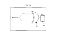
- the failure of the original partial circuit can be detected by the observation flip-flop 104 (see FIG. 26), but when the same signal is input to the EXOR tree 103, Since the signals cancel each other as described above, the observation flip-flop 104 cannot detect the failure of the original partial circuit (see FIG. 27). Therefore, in the case of the same signal, an observation flip-flop 104 that is electrically connected to another EXOR tree 103 and the other EXOR tree 103 is generated so that the same signal is not input to one EXOR tree 103. It is possible not to lower the failure detection rate. However, since the number of observation flip-flops 104 is increased, there is a problem that many resources of the observation flip-flops 104 are required.
- An object of the present invention is to provide a technique capable of improving a failure detection rate in a layout automatic design process of a DFT circuit.
- a method for designing a semiconductor integrated circuit is a method for designing a semiconductor integrated circuit including an observation circuit for detecting a circuit failure, (A) performing logical grouping to form a plurality of clusters for each signal line close to the logical hierarchy; (B) a step of reading an initial information group necessary for the stochastic grouping; (C) determining a maximum number of fan-ins electrically connected to one AND tree or one OR tree, and including the maximum number of fan-ins in the initial information group; (D) performing the stochastic grouping based on the initial information group to create grouping information of the signal lines; (E) a step of automatically arranging the signal lines based on the grouping information to form a layout of the signal lines; (F) After the step (e), a step of combining the signal lines with the AND tree or the OR tree based on the grouping information; (G) arranging the observation circuit at the end of the AND tree or the OR tree and performing a scan connection; Including The initial information group includes netlist,
- the software according to the present invention is software for designing a semiconductor integrated circuit including an observation circuit for detecting a circuit failure, (A) performing logical grouping to form a plurality of clusters for each signal line close to the logical hierarchy; (B) a step of reading an initial information group necessary for the stochastic grouping; (C) determining a maximum number of fan-ins electrically connected to one AND tree or one OR tree, and including the maximum number of fan-ins in the initial information group; (D) performing the stochastic grouping based on the initial information group to create grouping information of the signal lines; (E) a step of automatically arranging the signal lines based on the grouping information to form a layout of the signal lines; (F) After the step (e), a step of combining the signal lines with the AND tree or the OR tree based on the grouping information; (G) arranging the observation circuit at the end of the AND tree or the OR tree and performing a scan connection; Designing the semiconductor integrated circuit by a process including: The initial information group includes net
- the failure detection rate in the DFT circuit layout automatic design process can be improved.
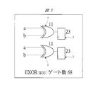
- FIG. 5 is an explanatory diagram when the tree circuit shown in FIG. 4 is configured by an EXOR tree circuit.
- FIG. 5 is an explanatory diagram when the tree circuit shown in FIG.
- FIG. 12 is an explanatory diagram illustrating an example in which the signal lines collected in FIG. 11 are aggregated to configure an AND tree circuit.
- FIG. 12 is an explanatory diagram illustrating an example in which the signal lines collected in FIG. 11 are aggregated to configure an OR tree circuit. It is explanatory drawing shown about the case where each signal line is aggregated in the AND tree circuit 1 after inserting an inverter in one signal line.
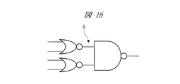
- FIG. 3 is an explanatory diagram showing a NAND-NOR circuit that is an equivalent circuit of an AND tree circuit.
- FIG. 3 is an explanatory diagram showing a NOR-NAND circuit that is an equivalent circuit of an OR tree circuit. It is explanatory drawing which shows the logical tree structure of the chip
- FIG. 24 is a flowchart illustrating details of a DFT circuit layout design process in the flowchart shown in FIG. 23. It is explanatory drawing which shows the example of observation of an enable signal. It is explanatory drawing which shows the characteristic of EXOR tree. It is explanatory drawing which shows the characteristic of EXOR tree.
- the constituent elements are not necessarily indispensable unless otherwise specified and apparently essential in principle. Needless to say.
- “consisting of A” and “consisting of A” do not exclude other elements unless specifically stated that only the elements are included. Needless to say.
- This embodiment relates to a failure detection process by observing an enable signal in an automatic layout design process (for example, EDA (Electronic Design Automation)) of a DFT circuit (observation circuit) using software.
- EDA Electronic Design Automation
- the signal line of the DFT circuit is aggregated by the EXOR tree circuit, and the failure is detected by receiving the signal from the EXOR tree circuit by the observation flip-flop circuit.
- the failure is detected by receiving the signal from the EXOR tree circuit by the observation flip-flop circuit.
- the signals may cancel each other, and the fault of the original partial circuit may not be detected.
- the signal lines of the DFT circuit aggregated by the EXOR tree circuit are aggregated by the AND tree circuit or the OR tree circuit instead of the EXOR tree circuit, thereby preventing a failure detection rate from being lowered.
- the AND tree circuit or the OR tree circuit in the present embodiment will be described.
- the probability of “1” at the first stage input of the tree circuit is halved, the probability c0 that “0” occurs at each stage of the tree circuit, and the probability c1 that “1” occurs at each stage of the tree circuit And calculate. From the calculation result, the probability c0 of occurrence of “0” in the final stage is compared with the probability c1 of occurrence of “1” in the final stage, and the probability c1 of occurrence of “1” in the final stage is large.
- the AND tree circuit 1 is configured and the output from the AND tree circuit 1 is received by the observation flip-flop 2 (see FIG. 1). If the probability c0 of occurrence of “0” in the final stage is large, OR is performed.
- the tree circuit 3 is configured and the output from the OR tree circuit 3 is received by the observation flip-flop 2 (see FIG. 2).
- the failure detection rate can be improved as compared with the case where the EXOR tree circuit is used.
- the signal is masked by the EXOR tree circuit 5 and the failure is caused by the observation flip-flop 2. Detection is not possible. For example, when one enable signal (fault) is simply grouped into all the observation flip-flops 2 in an even number, the fault detection rate of the enable logic generation circuit 4 is zero.
- the failure detection rate can be 100% because the failure is not masked.
- the AND tree circuit 1 or the OR tree circuit 3 when used, the number of gates constituting the tree circuit can be greatly reduced as compared with the case where the EXOR tree circuit 5 is used, and the chip size is reduced. Can be This will be described with reference to FIGS.
- the EXOR tree circuit 5 needs to be put together appropriately so as to trace the enable logic so that the original logic is different, and the observation flip-flop 2 must also be added if necessary. Therefore, if the tree circuit 6 shown in FIG. 4 is formed from the EXOR tree circuit 5, two EXOR tree circuits 5 are required, and the observation flip-flop 2 is also connected to each EXOR tree circuit 5. It becomes. In one EXOR tree circuit 5 and one observation flip-flop 2, the number of gates is 11 and 23, respectively. Therefore, the number of gates in the entire circuit structure shown in FIG. The numbers attached to the EXOR tree circuit 5 and the observation flip-flop 2 are the numbers of the respective gates. The tree structure when the EXOR tree circuit 5 is used becomes more complex as the enable logic increases, and the added observation flip-flop 2 also increases in proportion thereto.
- the AND logic circuit 4 A, 4 B, and 4 C can be connected by one AND tree circuit 1. Signals can be collected, and only one observation flip-flop 2 can be used.
- one AND tree circuit 1 and one observation flip-flop 2 are 8 and 23, respectively, so that the number of gates in the entire circuit structure shown in FIG. Note that the number appended to the AND tree circuit 1 is the number of gates of the AND tree circuit 1. That is, by forming the tree circuit 6 from the AND tree circuit 1, the number of gates can be significantly reduced as compared with the case where the tree circuit 6 is formed from the EXOR tree circuit 5. As a result, since the number of wirings can be reduced in the chip, the chip can be reduced in size.
- the test length may be longer than when a tree structure is constructed with an EXOR circuit.
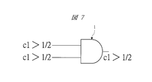
- This can be dealt with by changing the combination of the enable signals. That is, in consideration of the probability c0 of occurrence of “0” in each stage of the tree structure and the probability c1 of occurrence of “1” in each stage of the tree circuit, a signal having a probability c1 greater than 1 ⁇ 2 is AND tree.
- a signal having a probability c1 greater than 1 ⁇ 2 is AND tree.
- an inverter is added to the signal having the probability c1 less than 1/2 to the AND tree circuit 1. If it is necessary to consolidate signals with a probability c0 larger than 1/2 and signals with a smaller probability c0 into the OR tree circuit 3, an inverter is converted into a signal with a probability c0 smaller than 1/2. To the OR tree circuit 3 (see FIG. 10).
- FIG. 11 illustrates a case where signals collected in the AND tree circuit 1 are collected.
- the collected signal lines are aggregated, and an AND tree circuit 1 (see FIG. 12) or an OR tree circuit 3 (see FIG. 13) is configured, and then cost calculation is performed.
- the aggregation condition at this time is that signal lines with probability c1 greater than 1 ⁇ 2 are aggregated into AND tree circuit 1, and signal lines with probability c0 greater than 1 ⁇ 2 are
- the inverters are added and aggregated. To do.
- the one with the highest probability c1, c0 is selected from each tree circuit (AND tree circuit 1 and OR tree circuit 3). Thereby, since the pattern length of the tree structure can be reduced, the manufacturing cost can be reduced. At this time, if the probability (failure detection rate) c1 and c0 can be maximized in the tree circuit by inserting an inverter in the signal line, the tree circuit is selected after inserting the inverter in the signal (see FIG. 14).
- FIG. 14 illustrates a case where the signal lines are aggregated by the AND tree circuit 1 after an inverter is inserted into one signal line.
- (1) to (3) are given as examples of how to assign the initial value of the probability c0 of occurrence of “0” and the probability c1 of occurrence of “1” when calculating the probability of each enable logic. it can.
- Probabilities c0 and c1 at the inputs of the first stage of the tree structure and the outputs of the flip-flops are each halved and propagated.
- Toggle information is input to the input of each gate of the tree structure. Toggle information may be given only to some inputs of the tree structure and propagated otherwise.
- a random (random number) is given to the input of each gate of the tree structure. Random numbers (random numbers) may be given to only a part of the tree structure input, and the others may be propagated.
- the enable signals to which the initial values of the probabilities c0 and c1 are given are collected by the AND tree circuit 1 or the OR tree circuit 3.
- any enable signals can be combined.
- the enable signals are combined by the AND tree circuit 1 or the OR tree circuit 3, the following (a ), Pay attention to (b).
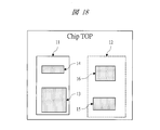
- FIGS. 17 and 18 show a logic tree structure and a circuit cell layout of a chip having a CPU (Central Processing Unit) 11 and a graphics operation unit 12, respectively.
- CPU Central Processing Unit
- the observation signals are grouped near the logical hierarchy, and the arrangement of the circuit cells is also performed in consideration of the logical hierarchy. That is, logically, the core circuit 13 and the cache memory circuit 14 are grouped by the CPU 11, and the VPU (Visual Processing Unit) 15 and the multiplier 16 are grouped by the graphics calculation unit 12. Further, the CPU 11 and the graphics calculation unit 12 are logically integrated into one chip.
- the CPU 11 and the graphics calculation unit 12 are logically integrated into one chip.
- the observation signal lines are selected so that the distribution area becomes smaller based on the circuit cell layout information for creating the circuit cell layout, the number of observation signal lines and the fanout. Specify a number.
- the observation signal lines are grouped so that the probability of detecting a failure is the highest. That is, the grouping and tree configuration is performed through the following procedures (b1) to (b3), for example.
- the threshold value of the observation signal lines to be collected in one observation flip-flop 2 (the maximum value of the number of fan-ins to be collected in one tree) is determined.
- the observation signal lines close to each other are grouped by the number of fan-ins within the threshold value of the observation signal lines to be collected in one observation flip-flop 2 determined in (b1) above.
- observation signal lines having the probability c1 of occurrence of “1” of 1/2 or more are collected, they become candidates for the AND tree circuit 1, and the probability c0 of occurrence of “0” is 1/2.
- the observation signal lines as described above are collected, they become candidates for the OR tree circuit 3.
- the observation signal line is an inverter. Is connected to the AND tree circuit 1.
- the observation signal line is connected to the inverter.
- a circuit cell layout is created. After the circuit cell layout is created, re-grouping and re-tree configuration of the observation signal lines are performed along the above (b1) to (b3) only between the circuit cells arranged in the vicinity. If the above (b1) to (b3) are not taken into consideration before the creation of the circuit cell layout, clustering is performed between circuit cells arranged in the vicinity from the arrangement state of each circuit cell after the creation of the circuit cell layout. Then, the observation signal lines are grouped so that the probability c1 of occurrence of “1” or the probability c0 of occurrence of “0” is increased, and the observation signal lines are combined into the AND tree circuit 1 or the OR tree circuit 3.
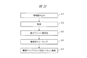
- an initial information group necessary for logical grouping and stochastic grouping is read (step S1).
- examples of the initial information group include netlist, cluster information, toggle information, timing constraints, and constraint information for forming a circuit cell layout.
- netlist refers to information (or a file) describing the function of the chip by the connection of primitive logic elements (such as AND and OR) and signal nets.
- the functions are clustered for each function, summarized as a group of logic (functions), and the connection is taken into consideration in the logical tree structure. Therefore, the logical tree structure is better than the netlist. The level of abstraction is higher.
- step S2 logical grouping is performed to form a plurality of clusters for each observation signal line that is close to the logical hierarchy (step S2).
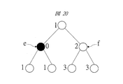
- a logical tree structure is created and clustered for each signal line close to the logical hierarchy to form a plurality of clusters. This will be described in more detail using the logical tree structure shown in FIG.
- an arbitrary enable signal e is selected, and the logical coupling level in the same hierarchy as that enable signal e is set to zero.
- Logically separated so that the coupling level of the enable signal in the hierarchy directly connected from the hierarchy is 1, and the coupling level of the enable signal in the hierarchy that is further moved from there is 2.
- the value of the coupling level increases as the enable signal of the hierarchy having the relationship.
- L [e] [f] 2 (“L” is a logical coupling degree between e and f, logical Indicates the distance of the hierarchy).
- L is a logical coupling degree between e and f, logical Indicates the distance of the hierarchy.
- ⁇ L [ei that is the sum of L [ei] [ej] between arbitrary enable signals ei and ej. ] [Ej] forms a cluster of enable signals so as to minimize.
- the maximum number of observation signal lines connected to one observation flip-flop 2, that is, the maximum fan-in number is determined and included in the aforementioned initial information group (step S3).
- the maximum fan-in number in this case affects the test cost. If the maximum fan-in number is large, the test cost increases, but the number of gates decreases. If the maximum fan-in number is small, the test cost decreases. However, the number of gates increases. That is, since the maximum fan-in number is a trade-off between circuit integration rate and test cost, it is selected depending on which of the circuit integration rate and test cost is important depending on the application of the chip.
- step S4 stochastic grouping is performed based on the above-described initial information group (step S4).
- the observation signal lines in the cluster are stochastically divided so that the number of fan-ins is less than the maximum fan-in number (fan-in number (first fan-in number)).
- the number of fan-ins at this time is generally a numerical value that is a factorial of 2, such as 4, 8, 16,. If the number of fan-ins is small, a failure can be detected with a small test length, but on the other hand, a large amount of circuit resources are required, and the fan-in number and test length and the corresponding circuit resources have a trade-off relationship. Become.
- the user determines the number of fan-ins as appropriate in consideration of circuit resources.
- the stochastic grouping in each cluster is performed when the probability (first probability) c1 of occurrence of “1” is larger than 1 ⁇ 2 at the final stage of the tree circuit.
- the AND tree circuit 1 When the probability of occurrence of “0” (second probability) c0 is greater than 1 ⁇ 2, the OR tree circuit 3 summarizes them.
- the observation signal lines in the cluster are stochastically grouped, they are collected and grouped in descending order of the probability c1 that “1” occurs or the probability c0 that “0” occurs.
- the AND tree circuit 1 and the OR tree circuit 3 are automatically arranged based on the constraint information for forming the circuit cell layout included in the initial information group described above, and the layout of each signal line, that is, A circuit cell layout is formed (step S5).
- the tree structure of the AND tree circuit 1 and the OR tree circuit 3 collected in step S4 may be reconfigured, and the AND tree circuit 1 and the OR tree circuit 3 may be combined again (step S6). ). That is, after forming a circuit cell layout and arranging each signal line, optimization of timing operation or the like may be executed. In such a case, the physical arrangement position of the signal line is also changed. Sometimes. At that time, by reconfiguring the group of enable signals, there are cases where wiring resources can be reduced and transition measures can be taken.
- both AND tree circuits 1 or OR tree circuits When the total wiring length of 3 is shortened, the tree structure of the AND tree circuit 1 and the OR tree circuit 3 collected in step S4 is reconfigured (see FIG. 21).
- observation flip-flop 2 is arranged at the end of the AND tree circuit 1 and the OR tree circuit 3, and these are connected by scanning (step S7).
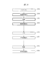
- an initial information group necessary for probabilistic grouping is read (step S11).
- the initial information group read here includes substantially the same information as the initial information group read in step S1 in FIG.
- Step S12 the circuit cells are arranged based on the constraint information for forming the circuit cell layout included in the initial information group read in step S11, and the layout of each signal line, that is, the circuit cell layout is formed.
- step S13 the maximum number of observation signal lines connected to one observation flip-flop 2, that is, the maximum number of fan-ins is determined and included in the aforementioned initial information group.
- observation signal lines are grouped as described above, and the observation signal lines are grouped into the AND tree circuit 1 or the OR tree circuit 3 (step S14).
- the observation signal lines are probabilistically divided and grouped so that the number of fan-ins is less than or equal to the maximum fan-in number included in the initial information group (fan-in number).
- the stochastic grouping is performed by the AND tree circuit 1 when the probability c1 of occurrence of “1” is larger than 1/2 at the final stage of the tree circuit, and the probability c0 of occurrence of “0” is 1 /. If the value is larger than 2, the OR tree circuit 3 collects them, and in either case, the probability c1 of occurrence of “1” or the probability c0 of occurrence of “0” is collected and grouped in the descending order.
- observation flip-flop 2 is arranged at the end of the AND tree circuit 1 and the OR tree circuit 3, and these are connected by scanning (step S15).
- step S21 the function of the entire chip is designed (step S21).
- step S22 logic design is performed in accordance with the function of the entire chip designed in step S21 (step S22), and further synthesized into a logic circuit (step S23).
- step S23 a test circuit is inserted into the logic circuit synthesized in step S23 (step S24).
- step S25 a circuit cell layout is created (step S25).
- This step S25 includes the layout design process of the DFT circuit summarized in FIGS. 19 and 22, and step S25 is further subdivided as shown in the flowchart of FIG.
- step S25 a floor plan design for a chip is first performed (step S25A).
- step S25A constraint information for forming a circuit cell layout is created, and the constraint information can be included in the aforementioned initial information group.
- step S25B the circuit cell is optimized (step S25B).
- the optimization of this circuit cell corresponds to step S2 (logical grouping), step S3 (maximum fan-in number determination) and step S4 (probabilistic grouping) summarized using FIG.
- step S25C the optimized circuit cell is placed in the chip floor.
- This circuit cell placement step corresponds to step S5 summarized using FIG. 19 and step S12 summarized using FIG.
- step S25D After the circuit cell is placed in the chip floor, the circuit cell is optimized as necessary (step S25D).
- the optimization of this circuit cell includes step S6 (reconfiguration of the tree structure) summarized using FIG. 19, step S7 (arrangement and scan connection of observation flip-flop 2), and step S13 (rearranged using FIG. 22).
- step S14 probabilistic grouping
- step S15 arrangement of the observation flip-flop 2 and scan connection
- CTS clock tree synthesis
- step S25G wiring corresponding to the circuit cell that has been optimized in the chip floor is arranged on the layout.
- step S25H the circuit cell layout in step 25 is created by optimizing the wiring and circuit cells arranged as necessary.
- step S26 a mask for transferring the circuit pattern to the semiconductor wafer is manufactured.
- step S27 the semiconductor integrated circuit according to the present embodiment is manufactured through wafer processing and packaging processing (step S27) using the mask.
- the semiconductor integrated circuit design method and software of the present invention can be applied to a DFT circuit layout automatic design process in the manufacture of a chip having a logic (logic) circuit such as a SoC (System on chip) and a microcomputer.
- a logic (logic) circuit such as a SoC (System on chip) and a microcomputer.
Landscapes
- Engineering & Computer Science (AREA)
- Computer Hardware Design (AREA)
- Physics & Mathematics (AREA)
- Theoretical Computer Science (AREA)
- Evolutionary Computation (AREA)
- Geometry (AREA)
- General Engineering & Computer Science (AREA)
- General Physics & Mathematics (AREA)
- Semiconductor Integrated Circuits (AREA)
- Design And Manufacture Of Integrated Circuits (AREA)
Abstract
Description
(a)論理的グルーピングを行い、論理階層的に近い信号線毎に複数のクラスタを形成する工程、
(b)確率的グルーピングに必要な初期情報群を読み込む工程、
(c)1つのAND treeもしくは1つのOR treeに電気的に接続される最大ファンイン数を決定し、前記最大ファンイン数を前記初期情報群に含める工程、
(d)前記初期情報群を基に前記確率的グルーピングを行い、前記信号線のグルーピング情報を作成する工程、
(e)前記グルーピング情報を基に、前記信号線の自動配置を行い、前記信号線のレイアウトを形成する工程、
(f)前記(e)工程後、前記グルーピング情報を基に前記信号線を前記AND treeもしくは前記OR treeでまとめる工程、
(g)前記AND treeもしくは前記OR treeの終端に前記観測用回路を配置してスキャン接続する工程、
を含み、
前記初期情報群には、netlist、クラスタ情報、トグル情報、タイミング制約、および前記レイアウトを形成する上での制約情報が含まれ、
前記(d)工程は、
(d1)前記複数のクラスタのうちの第1のクラスタ中にて、信号が1となる第1の確率が1/2以上の前記信号線を前記第1の確率が大きい順に前記最大ファンイン数以内の第1のファンイン数集め、1つ以上の前記AND treeの候補を形成する工程、
(d2)前記第1クラスタ中にて、前記信号が0となる第2の確率が1/2以上の前記信号線を前記第2の確率が大きい順に前記第1のファンイン数集め、1つ以上の前記OR treeの候補を形成する工程、
を含むものである。
(a)論理的グルーピングを行い、論理階層的に近い信号線毎に複数のクラスタを形成する工程、
(b)確率的グルーピングに必要な初期情報群を読み込む工程、
(c)1つのAND treeもしくは1つのOR treeに電気的に接続される最大ファンイン数を決定し、前記最大ファンイン数を前記初期情報群に含める工程、
(d)前記初期情報群を基に前記確率的グルーピングを行い、前記信号線のグルーピング情報を作成する工程、
(e)前記グルーピング情報を基に、前記信号線の自動配置を行い、前記信号線のレイアウトを形成する工程、
(f)前記(e)工程後、前記グルーピング情報を基に前記信号線を前記AND treeもしくは前記OR treeでまとめる工程、
(g)前記AND treeもしくは前記OR treeの終端に前記観測用回路を配置してスキャン接続する工程、
を含む工程によって前記半導体集積回路を設計し、
前記初期情報群には、netlist、クラスタ情報、トグル情報、タイミング制約、および前記レイアウトを形成する上での制約情報が含まれ、
前記(d)工程は、
(d1)前記複数のクラスタのうちの第1のクラスタ中にて、信号が1となる第1の確率が1/2以上の前記信号線を前記第1の確率が大きい順に前記最大ファンイン数以内の第1のファンイン数集め、1つ以上の前記AND treeの候補を形成する工程、
(d2)前記第1クラスタ中にて、前記信号が0となる第2の確率が1/2以上の前記信号線を前記第2の確率が大きい順に前記第1のファンイン数集め、1つ以上の前記OR treeの候補を形成する工程、
を含むものである。
(1)tree構造の初段の各入力およびフリップフロップの出力における確率c0、c1をそれぞれ1/2とし、伝播させる。
(2)tree構造の各ゲートの入力にトグル情報を入力する。tree構造の一部の入力にのみトグル情報を与えて、それ以外では伝播させてもよい。
(3)tree構造の各ゲートの入力にランダム(乱数)にて与える。tree構造の一部の入力にのみランダム(乱数)にて与えて、それ以外では伝播させてもよい。
(a)チップ面積およびフリップフロップの個数といった物理的リソースを効率よく使用する。
(b)確率的に故障を検出しやすいように、テスト長を短縮するようにtree構造にまとめる。
(b1)1つの観測用フリップフロップ2にまとめる観測信号線のしきい値(1つのtreeにまとめるファンイン数の最大値)を決定する。
(b2)上記(b1)で決定した1つの観測用フリップフロップ2にまとめる観測信号線のしきい値内のファンイン数で、互いに近傍にある観測信号線をまとめる。この時、前述したように、“1”が発生する確率c1が1/2以上となる観測信号線を集めると、AND tree回路1の候補となり、“0”が発生する確率c0が1/2以上となる観測信号線を集めると、OR tree回路3の候補となる。
(b3)AND tree回路1の候補にまとめられた観測信号線中に、“1”が発生する確率c1が1/2未満となる観測信号線があった場合には、その観測信号線はインバータを介してAND tree回路1に接続する。また、OR tree回路3の候補にまとめられた観測信号線中に、“0”が発生する確率c0が1/2未満となる観測信号線があった場合には、その観測信号線はインバータを介してOR tree回路3に接続する。
Claims (12)
- 回路故障検出用の観測回路を含む半導体集積回路の設計方法であって、
(a)論理的グルーピングおよび確率的グルーピングに必要な初期情報群を読み込む工程、
(b)前記論理的グルーピングを行い、論理階層的に近い信号線毎に複数のクラスタを形成する工程、
(c)1つのAND treeもしくは1つのOR treeに電気的に接続される最大ファンイン数を決定し、前記最大ファンイン数を前記初期情報群に含める工程、
(d)前記初期情報群を基に前記確率的グルーピングを行い、前記信号線のグルーピング情報を作成する工程、
(e)前記グルーピング情報を基に、前記信号線の自動配置を行い、前記信号線のレイアウトを形成する工程、
(f)前記(e)工程後、前記グルーピング情報を基に前記信号線を前記AND treeもしくは前記OR treeでまとめる工程、
(g)前記AND treeもしくは前記OR treeの終端に前記観測用回路を配置してスキャン接続する工程、
を含み、
前記初期情報群には、netlist、クラスタ情報、トグル情報、タイミング制約、および前記レイアウトを形成する上での制約情報が含まれ、
前記(d)工程は、
(d1)前記複数のクラスタのうちの第1のクラスタ中にて、信号が1となる第1の確率が1/2以上の前記信号線を前記第1の確率が大きい順に前記最大ファンイン数以内の第1のファンイン数集め、1つ以上の前記AND treeの候補を形成する工程、
(d2)前記第1クラスタ中にて、前記信号が0となる第2の確率が1/2以上の前記信号線を前記第2の確率が大きい順に前記第1のファンイン数集め、1つ以上の前記OR treeの候補を形成する工程、
を含むことを特徴とする半導体集積回路の設計方法。 - 請求項1記載の半導体集積回路の設計方法において、
前記(d1)工程にて、前記AND treeの前記候補に、前記第1の確率が1/2未満の前記信号線を含める場合には、前記第1の確率が1/2未満の前記信号線にインバータを付加し、
前記(d2)工程にて、前記OR treeの前記候補に、前記第2の確率が1/2未満の前記信号線を含める場合には、前記第2の確率が1/2未満の前記信号線にインバータを付加することを特徴とする半導体集積回路の設計方法。 - 請求項1記載の半導体集積回路の設計方法において、
前記(f)工程では、前記AND treeおよび前記OR treeの少なくとも一方は等価回路で形成し、
前記AND treeの前記等価回路は、NAND-NOR treeであり、
前記OR treeの前記等価回路は、NOR-NAND treeであることを特徴とする半導体集積回路の設計方法。 - 請求項1記載の半導体集積回路の設計方法において、
前記(e)工程では、前記(f)工程で前記AND treeもしくは前記OR treeにまとめられる前記信号線同士が近接するように、前記信号線の前記レイアウトを形成することを特徴とする半導体集積回路の設計方法。 - 請求項1記載の半導体集積回路の設計方法において、
前記第1のファンイン数は、前記AND treeもしくは前記OR treeにまとめられる前記信号線同士が近接するように決定することを特徴とする半導体集積回路の設計方法。 - 回路故障検出用の観測回路を含む半導体集積回路の設計方法であって、
(a)確率的グルーピングに必要な初期情報群を読み込む工程、
(b)信号線の自動配置を行い、前記信号線のレイアウトを形成し、前記信号線から複数のクラスタを形成する工程、
(c)1つのAND treeもしくは1つのOR treeに電気的に接続される最大ファンイン数を決定し、前記最大ファンイン数を前記初期情報群に含める工程、
(d)前記初期情報群を基に前記確率的グルーピングを行い、前記信号線のグルーピング情報を作成する工程、
(e)前記グルーピング情報を基に前記信号線を前記AND treeもしくは前記OR treeでまとめる工程、
(f)前記AND treeもしくは前記OR treeの終端に前記観測用回路を配置してスキャン接続する工程、
を含み、
前記初期情報群には、netlist、クラスタ情報、トグル情報、タイミング制約、および前記レイアウトを形成する上での制約情報が含まれ、
前記(d)工程は、
(d1)前記複数のクラスタのうちの第1のクラスタ中にて、信号が1となる第1の確率が1/2以上の前記信号線を前記第1の確率が大きい順に前記最大ファンイン数以内の第1のファンイン数集め、1つ以上の前記AND treeの候補を形成する工程、
(d2)前記第1クラスタ中にて、前記信号が0となる第2の確率が1/2以上の前記信号線を前記第2の確率が大きい順に前記第1のファンイン数集め、1つ以上の前記OR treeの候補を形成する工程、
を含むことを特徴とする半導体集積回路の設計方法。 - 回路故障検出用の観測回路を含む半導体集積回路を設計するソフトウエアであって、
(a)論理的グルーピングおよび確率的グルーピングに必要な初期情報群を読み込む工程、
(b)前記論理的グルーピングを行い、論理階層的に近い信号線毎に複数のクラスタを形成する工程、
(c)1つのAND treeもしくは1つのOR treeに電気的に接続される最大ファンイン数を決定し、前記最大ファンイン数を前記初期情報群に含める工程、
(d)前記初期情報群を基に前記確率的グルーピングを行い、前記信号線のグルーピング情報を作成する工程、
(e)前記グルーピング情報を基に、前記信号線の自動配置を行い、前記信号線のレイアウトを形成する工程、
(f)前記(e)工程後、前記グルーピング情報を基に前記信号線を前記AND treeもしくは前記OR treeでまとめる工程、
(f)前記AND treeもしくは前記OR treeの終端に前記観測用回路を配置してスキャン接続する工程、
を含む工程によって前記半導体集積回路を設計し、
前記初期情報群には、netlist、クラスタ情報、トグル情報、タイミング制約、および前記レイアウトを形成する上での制約情報が含まれ、
前記(d)工程は、
(d1)前記複数のクラスタのうちの第1のクラスタ中にて、信号が1となる第1の確率が1/2以上の前記信号線を前記第1の確率が大きい順に前記最大ファンイン数以内の第1のファンイン数集め、1つ以上の前記AND treeの候補を形成する工程、
(d2)前記第1クラスタ中にて、前記信号が0となる第2の確率が1/2以上の前記信号線を前記第2の確率が大きい順に前記第1のファンイン数集め、1つ以上の前記OR treeの候補を形成する工程、
を含むことを特徴とするソフトウエア。 - 請求項7記載のソフトウエアにおいて、
前記(d1)工程にて、前記AND treeの前記候補に、前記第1の確率が1/2未満の前記信号線を含める場合には、前記第1の確率が1/2未満の前記信号線にインバータを付加し、
前記(d2)工程にて、前記OR treeの前記候補に、前記第2の確率が1/2未満の前記信号線を含める場合には、前記第2の確率が1/2未満の前記信号線にインバータを付加することを特徴とするソフトウエア。 - 請求項7記載のソフトウエアにおいて、
前記(f)工程では、前記AND treeおよび前記OR treeの少なくとも一方は等価回路で形成し、
前記AND treeの前記等価回路は、NAND-NOR treeであり、
前記OR treeの前記等価回路は、NOR-NAND treeであることを特徴とするソフトウエア。 - 請求項7記載のソフトウエアにおいて、
前記(e)工程では、前記(f)工程で前記AND treeもしくは前記OR treeにまとめられる前記信号線同士が近接するように、前記信号線の前記レイアウトを形成することを特徴とするソフトウエア。 - 請求項7記載のソフトウエアにおいて、
前記第1のファンイン数は、前記AND treeもしくは前記OR treeにまとめられる前記信号線同士が近接するように決定することを特徴とするソフトウエア。 - 回路故障検出用の観測回路を含む半導体集積回路を設計するソフトウエアであって、
(a)確率的グルーピングに必要な初期情報群を読み込む工程、
(b)信号線の自動配置を行い、前記信号線のレイアウトを形成し、前記信号線から複数のクラスタを形成する工程、
(c)1つのAND treeもしくは1つのOR treeに電気的に接続される最大ファンイン数を決定し、前記最大ファンイン数を前記初期情報群に含める工程、
(d)前記初期情報群を基に前記確率的グルーピングを行い、前記信号線のグルーピング情報を作成する工程、
(e)前記グルーピング情報を基に前記信号線を前記AND treeもしくは前記OR treeでまとめる工程、
(f)前記AND treeもしくは前記OR treeの終端に前記観測用回路を配置してスキャン接続する工程、
を含む工程によって前記半導体集積回路を設計し、
前記初期情報群には、netlist、クラスタ情報、トグル情報、タイミング制約、および前記レイアウトを形成する上での制約情報が含まれ、
前記(d)工程は、
(d1)前記複数のクラスタのうちの第1のクラスタ中にて、信号が1となる第1の確率が1/2以上の前記信号線を前記第1の確率が大きい順に前記最大ファンイン数以内の第1のファンイン数集め、1つ以上の前記AND treeの候補を形成する工程、
(d2)前記第1クラスタ中にて、前記信号が0となる第2の確率が1/2以上の前記信号線を前記第2の確率が大きい順に前記第1のファンイン数集め、1つ以上の前記OR treeの候補を形成する工程、
を含むことを特徴とするソフトウエア。
Priority Applications (3)
| Application Number | Priority Date | Filing Date | Title |
|---|---|---|---|
| JP2010543740A JP5297468B2 (ja) | 2008-12-26 | 2008-12-26 | 半導体集積回路の設計方法およびソフトウエア |
| PCT/JP2008/073828 WO2010073399A1 (ja) | 2008-12-26 | 2008-12-26 | 半導体集積回路の設計方法およびソフトウエア |
| US13/141,986 US8434042B2 (en) | 2008-12-26 | 2008-12-26 | Method and software for designing semiconductor integrated circuit including observation circuit for detecting circuit failure |
Applications Claiming Priority (1)
| Application Number | Priority Date | Filing Date | Title |
|---|---|---|---|
| PCT/JP2008/073828 WO2010073399A1 (ja) | 2008-12-26 | 2008-12-26 | 半導体集積回路の設計方法およびソフトウエア |
Publications (1)
| Publication Number | Publication Date |
|---|---|
| WO2010073399A1 true WO2010073399A1 (ja) | 2010-07-01 |
Family
ID=42287066
Family Applications (1)
| Application Number | Title | Priority Date | Filing Date |
|---|---|---|---|
| PCT/JP2008/073828 Ceased WO2010073399A1 (ja) | 2008-12-26 | 2008-12-26 | 半導体集積回路の設計方法およびソフトウエア |
Country Status (3)
| Country | Link |
|---|---|
| US (1) | US8434042B2 (ja) |
| JP (1) | JP5297468B2 (ja) |
| WO (1) | WO2010073399A1 (ja) |
Cited By (2)
| Publication number | Priority date | Publication date | Assignee | Title |
|---|---|---|---|---|
| KR100682018B1 (ko) * | 2005-05-18 | 2007-02-13 | 제주대학교 산학협력단 | 고온, 고압 가열장치 및 고온, 고압 가열장치에 수용되는재생용기 |
| JP2013079912A (ja) * | 2011-10-05 | 2013-05-02 | Fujitsu Semiconductor Ltd | 半導体集積回路及び半導体集積回路の設計方法 |
Families Citing this family (3)
| Publication number | Priority date | Publication date | Assignee | Title |
|---|---|---|---|---|
| US8910097B2 (en) | 2012-12-31 | 2014-12-09 | Synopsys, Inc. | Netlist abstraction |
| US10169523B2 (en) * | 2015-08-27 | 2019-01-01 | International Business Machines Corporation | Timing constraints formulation for highly replicated design modules |
| US12366605B2 (en) | 2023-01-24 | 2025-07-22 | Stmicroelectronics International N.V. | Area, cost, and time-effective scan coverage improvement |
Citations (3)
| Publication number | Priority date | Publication date | Assignee | Title |
|---|---|---|---|---|
| JPH10124564A (ja) * | 1996-08-28 | 1998-05-15 | Matsushita Electric Ind Co Ltd | 検査容易化設計方法、バスエラー回避設計方法及び集積回路 |
| JP2006308302A (ja) * | 2005-04-26 | 2006-11-09 | Nec Electronics Corp | マスク回路及びマスク制御回路並びにマスク方法 |
| JP2007103662A (ja) * | 2005-10-04 | 2007-04-19 | Matsushita Electric Ind Co Ltd | 半導体集積回路およびその製造方法 |
Family Cites Families (7)
| Publication number | Priority date | Publication date | Assignee | Title |
|---|---|---|---|---|
| KR940007240B1 (ko) * | 1992-02-21 | 1994-08-10 | 현대전자산업 주식회사 | 병렬 테스트 회로 |
| WO1998012655A1 (fr) * | 1996-09-17 | 1998-03-26 | Hitachi, Ltd. | Procede de configuration d'un circuit integre a semi-conducteur |
| JP2000055986A (ja) | 1998-08-07 | 2000-02-25 | Matsushita Electric Ind Co Ltd | 半導体集積回路の設計方法 |
| JP2003014818A (ja) | 2001-07-02 | 2003-01-15 | Matsushita Electric Ind Co Ltd | スキャンテスト回路、及びスキャンテスト回路の作成方法 |
| JP2005223171A (ja) | 2004-02-06 | 2005-08-18 | Matsushita Electric Ind Co Ltd | 半導体集積回路のスキャンチェーン接続方法 |
| JP2005274500A (ja) | 2004-03-26 | 2005-10-06 | Matsushita Electric Ind Co Ltd | 検査容易化設計の半導体集積回路および半導体集積回路の故障箇所診断方法 |
| US7176718B1 (en) * | 2005-01-21 | 2007-02-13 | Altera Corporation | Organizations of logic modules in programmable logic devices |
-
2008
- 2008-12-26 JP JP2010543740A patent/JP5297468B2/ja not_active Expired - Fee Related
- 2008-12-26 WO PCT/JP2008/073828 patent/WO2010073399A1/ja not_active Ceased
- 2008-12-26 US US13/141,986 patent/US8434042B2/en not_active Expired - Fee Related
Patent Citations (3)
| Publication number | Priority date | Publication date | Assignee | Title |
|---|---|---|---|---|
| JPH10124564A (ja) * | 1996-08-28 | 1998-05-15 | Matsushita Electric Ind Co Ltd | 検査容易化設計方法、バスエラー回避設計方法及び集積回路 |
| JP2006308302A (ja) * | 2005-04-26 | 2006-11-09 | Nec Electronics Corp | マスク回路及びマスク制御回路並びにマスク方法 |
| JP2007103662A (ja) * | 2005-10-04 | 2007-04-19 | Matsushita Electric Ind Co Ltd | 半導体集積回路およびその製造方法 |
Cited By (2)
| Publication number | Priority date | Publication date | Assignee | Title |
|---|---|---|---|---|
| KR100682018B1 (ko) * | 2005-05-18 | 2007-02-13 | 제주대학교 산학협력단 | 고온, 고압 가열장치 및 고온, 고압 가열장치에 수용되는재생용기 |
| JP2013079912A (ja) * | 2011-10-05 | 2013-05-02 | Fujitsu Semiconductor Ltd | 半導体集積回路及び半導体集積回路の設計方法 |
Also Published As
| Publication number | Publication date |
|---|---|
| JP5297468B2 (ja) | 2013-09-25 |
| US8434042B2 (en) | 2013-04-30 |
| US20110265053A1 (en) | 2011-10-27 |
| JPWO2010073399A1 (ja) | 2012-05-31 |
Similar Documents
| Publication | Publication Date | Title |
|---|---|---|
| Ye et al. | TSV open defects in 3D integrated circuits: Characterization, test, and optimal spare allocation | |
| Choi et al. | Probe3. 0: A systematic framework for design-technology pathfinding with improved design enablement | |
| CN102879731B (zh) | 一种数字集成电路的测试方法 | |
| JP2005032102A (ja) | スキャンテスト設計方法、スキャンテスト回路、スキャンフリップフロップ回路、スキャンテスト回路挿入用cadプログラム、大規模集積回路及び携帯デジタル機器 | |
| US20130091483A1 (en) | Automatic flow of megacell generation | |
| JP5297468B2 (ja) | 半導体集積回路の設計方法およびソフトウエア | |
| CN107068661A (zh) | 半导体装置 | |
| US7562321B2 (en) | Method and apparatus for structured ASIC test point insertion | |
| US20020049958A1 (en) | Logical synthesizing apparatus for converting a hardware functional description into gate-level circuit information | |
| TWI722360B (zh) | 測試系統與測試方法 | |
| Nicolaidis et al. | Through-silicon-via built-in self-repair for aggressive 3D integration | |
| US6973631B2 (en) | Scan insertion with bypass login in an IC design | |
| US12007440B1 (en) | Systems and methods for scan chain stitching | |
| CN115408967A (zh) | 通过结构分析标识安全相关端口与其安全机制的关联 | |
| US20250208206A1 (en) | Automated low power cell insertion in dft-enabled multi power plane designs | |
| Sharma et al. | VLSI interconnects and their testing: prospects and challenges ahead | |
| US12367331B2 (en) | Approach to child block pinning | |
| CN209132386U (zh) | 扫描链电路系统与栅控正反器电路 | |
| Pasca et al. | Configurable thru-silicon-via interconnect built-in self-test and diagnosis | |
| JP6089853B2 (ja) | 配線検査装置、配線検査プログラム及び配線検査方法 | |
| Kim et al. | Hierarchical test compression for SOC designs | |
| Lepercq et al. | An interconnection network for a novel reconfigurable circuit board | |
| Jahanirad et al. | Effective fault detection in M3D ICs: a cluster-based BIST for enhanced inter-layer via fault coverage | |
| JP6051548B2 (ja) | 自動配置配線装置および自動配置配線方法 | |
| US7657857B2 (en) | Performance visualization of delay in circuit design |
Legal Events
| Date | Code | Title | Description |
|---|---|---|---|
| 121 | Ep: the epo has been informed by wipo that ep was designated in this application |
Ref document number: 08879194 Country of ref document: EP Kind code of ref document: A1 |
|
| ENP | Entry into the national phase |
Ref document number: 2010543740 Country of ref document: JP Kind code of ref document: A |
|
| WWE | Wipo information: entry into national phase |
Ref document number: 13141986 Country of ref document: US |
|
| NENP | Non-entry into the national phase |
Ref country code: DE |
|
| 122 | Ep: pct application non-entry in european phase |
Ref document number: 08879194 Country of ref document: EP Kind code of ref document: A1 |