WO2010071031A1 - 配線構造体、半導体素子、配線基板、表示用パネル及び表示装置 - Google Patents
配線構造体、半導体素子、配線基板、表示用パネル及び表示装置 Download PDFInfo
- Publication number
- WO2010071031A1 WO2010071031A1 PCT/JP2009/070322 JP2009070322W WO2010071031A1 WO 2010071031 A1 WO2010071031 A1 WO 2010071031A1 JP 2009070322 W JP2009070322 W JP 2009070322W WO 2010071031 A1 WO2010071031 A1 WO 2010071031A1
- Authority
- WO
- WIPO (PCT)
- Prior art keywords
- layer
- wiring
- aluminum alloy
- wiring structure
- aluminum
- Prior art date
- Legal status (The legal status is an assumption and is not a legal conclusion. Google has not performed a legal analysis and makes no representation as to the accuracy of the status listed.)
- Ceased
Links
Images

Classifications
-
- H—ELECTRICITY
- H10—SEMICONDUCTOR DEVICES; ELECTRIC SOLID-STATE DEVICES NOT OTHERWISE PROVIDED FOR
- H10D—INORGANIC ELECTRIC SEMICONDUCTOR DEVICES
- H10D86/00—Integrated devices formed in or on insulating or conducting substrates, e.g. formed in silicon-on-insulator [SOI] substrates or on stainless steel or glass substrates
- H10D86/40—Integrated devices formed in or on insulating or conducting substrates, e.g. formed in silicon-on-insulator [SOI] substrates or on stainless steel or glass substrates characterised by multiple TFTs
- H10D86/441—Interconnections, e.g. scanning lines
-
- G—PHYSICS
- G02—OPTICS
- G02F—OPTICAL DEVICES OR ARRANGEMENTS FOR THE CONTROL OF LIGHT BY MODIFICATION OF THE OPTICAL PROPERTIES OF THE MEDIA OF THE ELEMENTS INVOLVED THEREIN; NON-LINEAR OPTICS; FREQUENCY-CHANGING OF LIGHT; OPTICAL LOGIC ELEMENTS; OPTICAL ANALOGUE/DIGITAL CONVERTERS
- G02F1/00—Devices or arrangements for the control of the intensity, colour, phase, polarisation or direction of light arriving from an independent light source, e.g. switching, gating or modulating; Non-linear optics
- G02F1/01—Devices or arrangements for the control of the intensity, colour, phase, polarisation or direction of light arriving from an independent light source, e.g. switching, gating or modulating; Non-linear optics for the control of the intensity, phase, polarisation or colour
- G02F1/13—Devices or arrangements for the control of the intensity, colour, phase, polarisation or direction of light arriving from an independent light source, e.g. switching, gating or modulating; Non-linear optics for the control of the intensity, phase, polarisation or colour based on liquid crystals, e.g. single liquid crystal display cells
- G02F1/133—Constructional arrangements; Operation of liquid crystal cells; Circuit arrangements
- G02F1/136—Liquid crystal cells structurally associated with a semi-conducting layer or substrate, e.g. cells forming part of an integrated circuit
- G02F1/1362—Active matrix addressed cells
- G02F1/136286—Wiring, e.g. gate line, drain line
-
- H—ELECTRICITY
- H10—SEMICONDUCTOR DEVICES; ELECTRIC SOLID-STATE DEVICES NOT OTHERWISE PROVIDED FOR
- H10D—INORGANIC ELECTRIC SEMICONDUCTOR DEVICES
- H10D86/00—Integrated devices formed in or on insulating or conducting substrates, e.g. formed in silicon-on-insulator [SOI] substrates or on stainless steel or glass substrates
- H10D86/40—Integrated devices formed in or on insulating or conducting substrates, e.g. formed in silicon-on-insulator [SOI] substrates or on stainless steel or glass substrates characterised by multiple TFTs
- H10D86/60—Integrated devices formed in or on insulating or conducting substrates, e.g. formed in silicon-on-insulator [SOI] substrates or on stainless steel or glass substrates characterised by multiple TFTs wherein the TFTs are in active matrices
-
- G—PHYSICS
- G02—OPTICS
- G02F—OPTICAL DEVICES OR ARRANGEMENTS FOR THE CONTROL OF LIGHT BY MODIFICATION OF THE OPTICAL PROPERTIES OF THE MEDIA OF THE ELEMENTS INVOLVED THEREIN; NON-LINEAR OPTICS; FREQUENCY-CHANGING OF LIGHT; OPTICAL LOGIC ELEMENTS; OPTICAL ANALOGUE/DIGITAL CONVERTERS
- G02F1/00—Devices or arrangements for the control of the intensity, colour, phase, polarisation or direction of light arriving from an independent light source, e.g. switching, gating or modulating; Non-linear optics
- G02F1/01—Devices or arrangements for the control of the intensity, colour, phase, polarisation or direction of light arriving from an independent light source, e.g. switching, gating or modulating; Non-linear optics for the control of the intensity, phase, polarisation or colour
- G02F1/13—Devices or arrangements for the control of the intensity, colour, phase, polarisation or direction of light arriving from an independent light source, e.g. switching, gating or modulating; Non-linear optics for the control of the intensity, phase, polarisation or colour based on liquid crystals, e.g. single liquid crystal display cells
- G02F1/133—Constructional arrangements; Operation of liquid crystal cells; Circuit arrangements
- G02F1/136—Liquid crystal cells structurally associated with a semi-conducting layer or substrate, e.g. cells forming part of an integrated circuit
- G02F1/1362—Active matrix addressed cells
- G02F1/136286—Wiring, e.g. gate line, drain line
- G02F1/13629—Multilayer wirings
-
- G—PHYSICS
- G02—OPTICS
- G02F—OPTICAL DEVICES OR ARRANGEMENTS FOR THE CONTROL OF LIGHT BY MODIFICATION OF THE OPTICAL PROPERTIES OF THE MEDIA OF THE ELEMENTS INVOLVED THEREIN; NON-LINEAR OPTICS; FREQUENCY-CHANGING OF LIGHT; OPTICAL LOGIC ELEMENTS; OPTICAL ANALOGUE/DIGITAL CONVERTERS
- G02F1/00—Devices or arrangements for the control of the intensity, colour, phase, polarisation or direction of light arriving from an independent light source, e.g. switching, gating or modulating; Non-linear optics
- G02F1/01—Devices or arrangements for the control of the intensity, colour, phase, polarisation or direction of light arriving from an independent light source, e.g. switching, gating or modulating; Non-linear optics for the control of the intensity, phase, polarisation or colour
- G02F1/13—Devices or arrangements for the control of the intensity, colour, phase, polarisation or direction of light arriving from an independent light source, e.g. switching, gating or modulating; Non-linear optics for the control of the intensity, phase, polarisation or colour based on liquid crystals, e.g. single liquid crystal display cells
- G02F1/133—Constructional arrangements; Operation of liquid crystal cells; Circuit arrangements
- G02F1/136—Liquid crystal cells structurally associated with a semi-conducting layer or substrate, e.g. cells forming part of an integrated circuit
- G02F1/1362—Active matrix addressed cells
- G02F1/136286—Wiring, e.g. gate line, drain line
- G02F1/136295—Materials; Compositions; Manufacture processes
-
- H—ELECTRICITY
- H10—SEMICONDUCTOR DEVICES; ELECTRIC SOLID-STATE DEVICES NOT OTHERWISE PROVIDED FOR
- H10D—INORGANIC ELECTRIC SEMICONDUCTOR DEVICES
- H10D30/00—Field-effect transistors [FET]
- H10D30/60—Insulated-gate field-effect transistors [IGFET]
- H10D30/67—Thin-film transistors [TFT]
- H10D30/6729—Thin-film transistors [TFT] characterised by the electrodes
- H10D30/6737—Thin-film transistors [TFT] characterised by the electrodes characterised by the electrode materials
-
- H—ELECTRICITY
- H10—SEMICONDUCTOR DEVICES; ELECTRIC SOLID-STATE DEVICES NOT OTHERWISE PROVIDED FOR
- H10D—INORGANIC ELECTRIC SEMICONDUCTOR DEVICES
- H10D30/00—Field-effect transistors [FET]
- H10D30/60—Insulated-gate field-effect transistors [IGFET]
- H10D30/67—Thin-film transistors [TFT]
- H10D30/6729—Thin-film transistors [TFT] characterised by the electrodes
- H10D30/6737—Thin-film transistors [TFT] characterised by the electrodes characterised by the electrode materials
- H10D30/6739—Conductor-insulator-semiconductor electrodes
-
- H—ELECTRICITY
- H10—SEMICONDUCTOR DEVICES; ELECTRIC SOLID-STATE DEVICES NOT OTHERWISE PROVIDED FOR
- H10D—INORGANIC ELECTRIC SEMICONDUCTOR DEVICES
- H10D30/00—Field-effect transistors [FET]
- H10D30/60—Insulated-gate field-effect transistors [IGFET]
- H10D30/67—Thin-film transistors [TFT]
- H10D30/674—Thin-film transistors [TFT] characterised by the active materials
- H10D30/6741—Group IV materials, e.g. germanium or silicon carbide
- H10D30/6743—Silicon
Definitions
- the present invention relates to a wiring structure, a semiconductor element, a wiring board, a display panel, and a display device. More specifically, the present invention relates to a wiring structure that can be suitably used for a display device having a transparent conductive film, a semiconductor element including the wiring structure, a wiring substrate, a display panel, and a display device.
- Wiring structures are used in electronic and electrical components as conductors for transmitting electrical signals and electric power.
- printed wiring boards, semiconductor devices, active matrix substrates for display devices, etc. constitute circuits and semiconductor elements. It is.
- a metal material having a low resistance and further having a low contact resistance with an electrode or a semiconductor connected to the wiring structure is preferably used. It is one of the metal materials preferably used.
- a transparent conductive film is used.
- ITO indium tin oxide
- the resistance of the connection portion may be increased due to the formation of aluminum oxide.
- mutual diffusion occurs at the interface with the insulating film or the like due to heating, which may deteriorate the characteristics.
- an aluminum layer and a barrier metal layer such as a titanium nitride film, a titanium film, and a molybdenum film are used as a wiring structure, so that an interface between the oxide electrode and the wiring structure is used.
- the formation of an oxide film was suppressed, and the interdiffusion at the interface with the insulating film etc. with which the wiring contacts was suppressed.
- an aluminum layer is formed and a titanium film or the like is formed, there has been a demand for a wiring structure capable of improving productivity and reducing costs.
- a semiconductor element used in a liquid crystal display device or the like for example, it has a portion where a semiconductor layer and an electrode layer are directly joined, and the electrode layer is a transition of nickel, cobalt, iron or the like.
- a semiconductor element formed of an aluminum alloy thin film containing a metal is disclosed (for example, see Patent Document 1).
- the single-layer wiring of the aluminum alloy thin film is connected to the semiconductor layer of the thin film transistor. The purpose is to suppress mutual diffusion between silicon constituting the semiconductor layer and elements constituting the electrode layer. is there.
- the aluminum alloy thin film containing carbon at least one element of nickel, cobalt, and iron contains 0.5 to 7.0 at% and carbon contains 0.1 to 3.0 at%
- An aluminum alloy thin film in which the balance is aluminum is disclosed (for example, see Patent Document 2).
- a thin film transistor disposed on a glass substrate, a pixel electrode formed by a transparent electrode, and an aluminum alloy film that electrically connects the thin film transistor and the pixel electrode, the aluminum alloy film and the pixel electrode are Part of alloy components constituting the aluminum alloy film at the contact interface in which the aluminum alloy film and the pixel electrode are in direct contact with each other, directly connected without a refractory metal composed of Mo, Cr, Ti, and W
- the display device in which all exist as a deposit or a concentrated layer is disclosed (for example, refer patent document 3).
- a conventional wiring using an aluminum alloy uses an aluminum alloy thin film as a single-layer wiring.
- it is necessary to form a thick aluminum alloy thin film.
- the aluminum alloy has a higher value compared with single aluminum, in order to reduce the cost. There is room for further improvement, and it has been desired to reduce the cost while improving the state at the interface with the oxide electrode, the insulating film, and the like.
- the present invention has been made in view of the above-described present situation, and an object thereof is to provide a wiring structure capable of achieving good connection with an oxide electrode and the like and reducing the cost. Is.
- the present inventors have made various studies on a wiring structure that can reduce the contact resistance even when connected to the oxide electrode and can further reduce the cost. Pay attention. And if the wiring is formed with an aluminum alloy single layer, the cost becomes high, and in the case of a structure in which an aluminum alloy layer and a titanium layer are laminated, the elements in the aluminum alloy diffuse into the titanium layer, It was found that the characteristics of the wiring deteriorated.
- an aluminum alloy layer can be connected to an oxide electrode to make a low-resistance contact. Further, for example, mutual diffusion at the interface with the insulating film or the like that is in contact with the wiring structure can be suppressed. Furthermore, by using only the surface layer in contact with the oxide electrode or the like as an aluminum alloy layer, the amount of aluminum alloy used can be reduced as compared with the case where an aluminum alloy single layer is used as wiring, thereby reducing costs.
- the inventors have found that a good connection with other electrodes and the like can be realized, and have conceived that the above-mentioned problems can be solved brilliantly, and have reached the present invention.
- the present invention is a laminate of two or more layers including at least one layer selected from the group consisting of an aluminum layer, a copper layer and a copper alloy layer, and an aluminum alloy layer, and the aluminum alloy layer is a surface layer.
- the wiring structure is arranged. The present invention is described in detail below.
- the wiring structure of the present invention is a laminate of two or more layers including at least one layer selected from the group consisting of an aluminum layer, a copper layer and a copper alloy layer, and an aluminum alloy layer, and the aluminum alloy layer is a surface layer. Is arranged. That is, in a wiring structure including at least one layer selected from the group consisting of an aluminum layer, a copper layer, and a copper alloy layer, the aluminum alloy layer is disposed on at least one surface side. In this case, it arrange
- An aluminum layer, a copper layer, and a copper alloy layer are preferably used as metal materials for forming wirings in various electric and electronic devices because they are excellent in electrical conductivity and relatively inexpensive.
- an oxide film for example, aluminum oxide or copper oxide
- an oxide film for example, aluminum oxide or copper oxide
- mutual diffusion may occur between an element constituting the wiring structure and an element constituting the insulating film at the interface with the insulating film or the like.
- the aluminum alloy layer provided on the surface layer and the oxide electrode can be connected, generation of an oxide film can be suppressed and contact resistance can be reduced.
- mutual diffusion can be suppressed by the aluminum alloy layer functioning as a barrier metal layer. In such a form, the effect which provides an aluminum alloy layer in a surface layer is exhibited more.
- an aluminum layer, a copper layer, a copper alloy layer, and the like are relatively inexpensive and excellent in electrical conductivity, a wiring structure having good characteristics can be formed at a low cost.
- the aluminum alloy layer only needs to be provided on the surface layer on at least one surface side of the wiring structure, and other layers forming the wiring structure include an inexpensive aluminum layer, a copper layer, a copper alloy layer, and the necessary Depending on the, other conductive layers can be used. Therefore, it is possible to increase the conductivity of the wiring structure, reduce the amount of high-value aluminum alloy used, and reduce the cost.
- the wiring structure has only to have a structure in which two or more layers including an aluminum alloy layer are arranged in contact with each other, and may have three or more layers.
- the aluminum alloy layer may be provided on the entire surface on one surface side of the wiring structure, or may be provided on a part of one surface side of the wiring structure.
- the contact resistance between the wiring structure and the oxide electrode can be reduced if an aluminum alloy layer is disposed at least at the portion connected to the oxide electrode. Can do.
- another member for example, an insulating film
- a form in which an aluminum alloy layer is disposed on the entire surface on one surface side of the wiring structure is preferable.
- the aluminum alloy layer is an alloy containing aluminum as a main component, for example, aluminum and another metal element, or an alloy of aluminum and a nonmetallic element such as carbon, nitrogen, or silicon.
- the element other than aluminum (hereinafter, also referred to as “addition element”) constituting the aluminum alloy layer may be one type or two or more types.
- the composition of the aluminum alloy layer is appropriately set depending on the type of element added to form an alloy, and for example, the aluminum content is preferably 50.0 at% or more and 99.5 at% or less. . That is, the element added to the aluminum alloy is preferably more than 0.5 at% and preferably less than 50.0 at%. Thereby, the characteristic as an alloy can be exhibited effectively, maintaining the outstanding electrical conductivity etc. as aluminum. For example, the contact resistance with the oxide electrode can be sufficiently reduced, and the mutual diffusion at the contact interface can be suppressed.
- the composition of the aluminum alloy can be measured by, for example, Auger electron spectroscopy, fluorescent X-ray EDX, or ICP-MS (inductively coupled plasma mass spectrometry).
- the additive element added to the aluminum alloy and the composition of the copper alloy can also be measured by the same method.
- the aluminum alloy layer has a thickness of 1 ⁇ 2 or less of the wiring structure.
- the aluminum alloy layer is provided as a thin film on the surface layer of the wiring structure. If the aluminum alloy layer is provided in a contact portion with an electrode layer such as an oxide electrode, the characteristics can be sufficiently exerted. However, since the aluminum alloy has a high value, the amount used can be reduced. preferable. Therefore, by using an aluminum alloy only for the upper layer thin film of the wiring structure, the cost can be reduced as compared with the case where the wiring is formed of an aluminum alloy single layer film.
- the aluminum alloy layer has a thickness that is half or less (1/2 or less) of other layers other than the aluminum alloy layer (if there are other layers, the total of the plurality of layers). Is preferred. Moreover, in order to fully exhibit the characteristics as an aluminum alloy layer, the thickness is preferably 10 nm or more. With such a thickness, even when connecting to an oxide electrode or the like, the contact resistance can be improved and the manufacturing cost can be reduced.
- the aluminum alloy layer disposed on the surface layer forms an aluminum alloy on the surface opposite to the surface on which other conductive layers (aluminum layer, copper layer, copper alloy layer, etc.) other than the aluminum alloy layer are disposed. It is preferable that the crystal
- the additive element diffuses on the surface of the aluminum alloy, and crystals of aluminum and the additive element are precipitated.
- the aluminum alloy contains Ni element, Al 3 Ni crystals are deposited on the surface, thereby suppressing formation of an oxide film.
- the temperature of the heat treatment may be appropriately set depending on the kind and amount of the element added to the aluminum alloy, but is preferably 200 to 400 ° C., for example.
- the wiring structure preferably includes an aluminum layer. That is, a wiring structure including an aluminum alloy layer and an aluminum layer is preferable. In the case where the aluminum alloy layer and the aluminum layer are stacked, the two-layer patterning for forming the wiring structure can be performed collectively by wet etching. For example, in the case of a wiring structure including a titanium layer or the like, it is preferable to use dry etching for patterning the titanium layer, but from the viewpoint of reducing manufacturing costs, patterning using wet etching is preferable. It is. Note that each of the aluminum layer and the aluminum alloy layer may be provided as one layer, or may be provided as two or more layers. For example, the structure of the wiring structure may be a three-layer structure of Al alloy / Al / Al alloy. Since the aluminum alloy layer can make a good connection with an oxide electrode or a semiconductor layer such as silicon, in such a structure, it is connected to the oxide electrode on one surface and the other surface. Then, connection with a semiconductor layer can also be performed.
- the aluminum layer is a layer substantially composed of only aluminum metal.
- elements may diffuse from other metal materials or interlayer insulating films that are in contact with the aluminum layer, so that a trace amount of impurity elements may be included.
- the manufacturing process is inexpensive compared to the case of patterning by dry etching. be able to.
- the wiring structure includes an aluminum layer and an aluminum alloy layer.
- the said copper layer is a layer comprised only with copper substantially.
- an element may diffuse from another metal material or an interlayer insulating film that is in contact with the copper layer, so that a trace amount of an impurity element may be included.
- the copper alloy layer includes copper as an essential component, and further includes other metal elements and nonmetal elements such as carbon and silicon.
- the type and amount of other elements in the copper alloy layer are not particularly limited, but the copper element in the copper alloy layer is preferably 50 at% or more, and preferably 99.5 at% or less. Examples of the element added to the copper alloy include Mg and Mn, but are not particularly limited, and may be appropriately set depending on the use of the wiring structure.
- the wiring structure is also suitable from the viewpoint of connection with a semiconductor film made of silicon or the like. According to this, since the metal element in the wiring structure can be prevented from diffusing into the semiconductor film, good ohmic characteristics can be obtained. For example, when an aluminum film and a silicon film are connected and heated, mutual diffusion may occur near the interface between the aluminum film and the silicon film. By connecting the silicon film with the aluminum alloy layer, a reaction layer of silicon (such as nickel) and silicon that forms the aluminum alloy layer is formed at the interface, thereby suppressing interdiffusion. Can do.
- the said wiring structure is used as wiring which comprises an electronic device etc., and has a structure where the conductive layer was laminated
- the wiring is a signal wiring for transmitting an electric signal, a power supply wiring for supplying power, a wiring constituting a circuit, a wiring for applying an electric field (for example, applying an electric field to the gate of a TFT), etc. It is not limited.
- a thin film transistor (TFT) includes a source / drain wiring, a gate wiring, and the like.
- a signal is transmitted like a gate wiring and an electric field is applied to a gate insulating film or the like. Shall also be included in “wiring”.
- the auxiliary capacitance wiring forms an auxiliary capacitance used for holding a voltage applied to the liquid crystal.
- a photosensor wiring is also a preferred mode.
- the aluminum alloy layer preferably contains a transition metal element.
- the transition metal element is an element of Group 3 to Group 11 of the periodic table.
- the transition metal element is a metal element whose d orbit or f orbit is not a closed shell, but it is more likely that crystals with aluminum easily precipitate on the surface of the aluminum alloy layer, and an oxide film is formed on the surface layer of the aluminum alloy layer. Interdiffusion occurring at the interface with other members can be suppressed by suppressing the heat resistance of the aluminum alloy layer.
- the transition metal element is not particularly limited, for example, nickel, iron, cobalt, titanium, vanadium, chromium, zirconium, niobium, molybdenum, ruthenium, rhodium, palladium, hafnium, tantalum, tungsten, osmium, iridium, Examples include various metal elements such as platinum and the like, lanthanoids and actinoids.
- the aluminum alloy layer preferably includes at least one selected from the group consisting of iron, cobalt, and nickel. Iron, cobalt and nickel are also called iron group elements and have similar properties.
- Elements such as nickel can easily deposit metal crystals on the surface of the aluminum alloy layer by heating or the like, can prevent the formation of aluminum oxide at the interface with the oxide electrode, and can reduce the contact resistance. .
- the aluminum alloy layer contains a transition metal element
- the content ratio of the transition metal element in the aluminum alloy layer is preferably 0.5 at% or more and less than 50 at%.
- the content is preferably 0.5 to 10.0 at%.
- the content of the neodymium, lanthanum, or the like is preferably 0.1 to 3.0 at%.
- the aluminum alloy layer preferably contains at least one element selected from the group consisting of Group 13 elements and Group 14 elements of the Periodic Table.
- Group 13 elements in the periodic table include boron, gallium, and indium.
- examples of the group 14 element in the periodic table include carbon, silicon, germanium, tin, and lead. Such an element is preferable in terms of improving the heat resistance of the aluminum alloy and easily forming a good alloy with the aluminum element.
- boron, carbon, and silicon are preferable additive elements.
- Such an additive element may be added together with the transition metal element, may be added alone, or is not particularly limited.
- the preferred range for the contents of Group 13 elements and Group 14 elements in the periodic table is not particularly limited, but is preferably 0.1 to 5.0 at%, for example.
- the wiring structure includes at least one layer selected from the group consisting of an aluminum layer, a copper layer, and a copper alloy layer, and an aluminum alloy layer.
- the additive element in the aluminum alloy layer and other conductive layers are included.
- the type and the combination thereof are not particularly limited, and may be set as appropriate depending on the application to be used.
- a wiring structure including an aluminum alloy layer including nickel as an additive element and an aluminum layer may be used, or a wiring structure including an aluminum alloy layer including silicon as an additive element and a copper layer. There is no particular limitation.
- a preferable form of the wiring structure is a laminated body of three or more layers, in which an aluminum alloy layer is disposed on both surface layers. That is, it is preferable that the wiring has an aluminum alloy layer provided on both sides of the wiring structure with another conductive layer such as an aluminum layer, a copper layer, or a copper alloy layer interposed therebetween. In this way, by arranging the aluminum alloy layers on both sides, the connection with the semiconductor layer such as an oxide electrode or silicon can be made favorable on both sides of the wiring structure. In addition, it is possible to prevent diffusion of elements such as aluminum at the interface with the insulating film or the like. For example, when a wiring structure is used as a source electrode of a TFT, the transistor characteristics are improved. can do.
- a preferred form of the wiring structure is a laminate of three or more layers, in which an aluminum alloy layer is provided on one surface and a titanium layer or a molybdenum layer is laminated on the opposite surface.
- the wiring structure includes an aluminum layer, a structure in which an aluminum alloy layer, an aluminum layer, and a titanium layer are laminated in this order, or a structure in which an aluminum alloy layer, an aluminum layer, and a molybdenum layer are laminated in this order.
- an additive element in the aluminum alloy layer is added to the titanium layer or the molybdenum layer. Diffusion can be suppressed. According to this, the characteristics of the wiring can be improved. For example, when the wiring is used as a source electrode of a TFT, the transistor characteristics can be improved. This may replace the aluminum layer with a copper layer or a copper alloy layer, and is not particularly limited.
- a preferred form of the wiring structure includes a form in which a titanium layer is laminated on the side opposite to the surface on which the aluminum alloy layer is disposed. Since molybdenum is a metal material that is more easily deteriorated by water or the like than titanium, it is preferable to use a titanium layer rather than a molybdenum layer from the viewpoint of stability.
- a preferable form of the wiring structure includes a form in which a molybdenum layer is laminated on the side opposite to the surface on which the aluminum alloy layer is disposed. Since the molybdenum layer can be patterned by using the same etching solution as aluminum, patterning can be performed together with aluminum and an aluminum alloy. Therefore, depending on the application in which the wiring structure is used, the manufacturing process can be simplified by using molybdenum, and productivity can be improved.
- the present invention is also a semiconductor element including the wiring structure and a semiconductor layer.
- the wiring structure as a wiring electrically connected to the semiconductor element, the contact resistance between the wiring structure and another electrode layer can be reduced, and the characteristics of the semiconductor element are improved. can do.
- 3 terminal elements such as 2 terminal elements, such as a diode, and a transistor, are mentioned.
- the semiconductor element is preferably a thin film transistor (TFT), and the wiring structure is preferably a source / drain wiring (source wiring and / or drain wiring).
- TFT thin film transistor
- the wiring structure is preferably a source / drain wiring (source wiring and / or drain wiring).
- the source / drain wiring electrically connected to the drain region of the TFT is connected to the pixel electrode constituting the display pixel.
- the pixel electrode uses an oxide electrode such as indium tin oxide or indium zinc oxide, the contact resistance can be reduced by connecting the aluminum alloy layer of the wiring structure and the oxide electrode. Can do.
- the additive element of the aluminum alloy is particularly preferably nickel, iron, cobalt or the like.
- the aluminum alloy containing nickel can suppress the formation of an oxide film at the interface with the oxide electrode due to precipitation of Al 3 Ni crystals by heat treatment or the like.
- the semiconductor element is preferably a thin film transistor, and the wiring structure is preferably a gate wiring.
- the aluminum alloy layer serves as a barrier metal layer, and the diffusion of elements into the aluminum layer can be suppressed.
- the barrier metal layer titanium, titanium nitride (TiN), or the like is used. When this is etched, dry etching is performed. However, since the aluminum alloy layer can be patterned by wet etching, the cost can be reduced as compared with the case of using dry etching. When used as a gate wiring, terminal corrosion becomes a problem, and therefore an aluminum alloy is required to have corrosion resistance and heat resistance.
- an additive element of the aluminum alloy it is preferable to include a transition metal element such as iron, nickel, or cobalt, and an additional element may be added to improve heat resistance or the like.
- Preferred examples of the additional element include neodymium and lanthanum.
- the wiring structure is preferably an auxiliary capacitance wiring.
- the auxiliary capacitance wiring is a wiring for constituting an auxiliary capacitance for holding a voltage applied to the liquid crystal.
- the auxiliary capacitor is formed by forming a capacitor with two conductive layers sandwiching an insulating film. One of the conductive layers (auxiliary capacitance wiring) constituting the auxiliary capacitance is connected to the pixel electrode.
- the uppermost layer of the drain wiring 120b is formed of the aluminum alloy layer 112b, so that the drain wiring 120b and the pixel electrode 107 are connected to each other. Can be connected directly. Therefore, the diameter of the contact hole can be reduced and the aperture ratio can be increased.
- the contact hole 15 is provided in the protective film 5 and the interlayer organic insulating film 6 formed on the structure in which the aluminum layer 11b is laminated on the titanium layer 10b, and the interlayer organic
- the pixel electrode 7 formed on the insulating film 6 and the source wiring 20a are connected, when the aluminum layer 11b and the pixel electrode 7 are directly connected, an oxide film is formed at the interface. Therefore, the aluminum layer 11b is etched to perform an etching process that exposes the surface of the titanium layer 10b, thereby connecting to the titanium layer. For this reason, the productivity is hindered due to an increase in the number of manufacturing steps, and the product yield (manufacturing yield) due to defective etching is reduced.
- the contact hole diameter is increased so that the contact between the pixel electrode and the drain wiring that also functions as the auxiliary capacitance wiring is made good, the width of the wiring connected to the pixel wiring also increases. An aperture ratio will fall.
- the present invention further relates to a wiring board in which the wiring structure, the insulating film, and the conductive film are arranged in this order on a substrate, and the wiring structure is made of an aluminum alloy through a contact hole provided in the insulating film. It is also a wiring board connected to the conductive film from the layer side. According to this, the aluminum alloy layer is disposed on the conductive film side of the wiring structure, the conductive film and the aluminum alloy layer are connected, and the contact resistance can be reduced. Thereby, the operation of the wiring board can be further stabilized.
- the substrate is not particularly limited, and various substrates can be used.
- a substrate such as a single crystal semiconductor substrate, an oxide single crystal substrate, a metal substrate, a glass substrate, a quartz substrate, or a resin substrate can be used.
- a conductive substrate such as a single crystal semiconductor substrate or a metal substrate, it is preferable to use an insulating film or the like provided thereon.
- the insulating film is provided between the wiring structure and the conductive film.
- the insulating film may be a single layer or two or more layers. In the case of two or more layers, a contact hole penetrating the two-layer insulating film is provided, and the wiring structure and the conductive film are connected.
- the material forming the insulating film is not particularly limited, and various insulating materials such as silicon oxide, silicon nitride, and an organic insulating material can be used.
- the conductive film is preferably an oxide electrode. According to this, since the aluminum alloy layer is disposed on the oxide electrode side of the wiring structure and the oxide electrode and the aluminum alloy layer are connected, the oxide film at the contact portion between the aluminum alloy layer and the oxide electrode Formation can be suppressed, and contact resistance can be reduced. Thereby, the operation of the wiring board can be further stabilized.
- the wiring structure, the insulating film, and the oxide electrode are preferably arranged in this order from the substrate side.
- a source / drain wiring or auxiliary capacitance wiring connected to the TFT
- the oxide electrode are arranged in this order from the substrate side.
- the wiring structure When the wiring structure is connected to the oxide electrode from the aluminum alloy layer side through a contact hole provided in the insulating film, generation of aluminum oxide between the oxide electrode and the wiring structure is suppressed.
- the contact resistance can be lowered.
- the oxide electrode is preferably a transparent conductive film.
- the wiring board can be suitably used as a substrate for a display device used in a display device.
- an oxide electrode such as indium tin oxide or indium zinc oxide is used as the transparent conductive film, the wiring structure according to the present invention can be preferably used.
- the transparent conductive film is preferably a wiring. According to this, since the elements constituting the wiring can be prevented from diffusing at the connection portion with the wiring structure, the connection between the wiring structure and the transparent conductive film can be improved. Thereby, the operation of the wiring board can be further stabilized.
- the wiring is not particularly limited, and examples thereof include wiring exemplified as a wiring structure.
- the wiring board preferably includes the semiconductor element described above. That is, the wiring board preferably includes a thin film transistor on the substrate, and the source / drain wiring of the thin film transistor is a wiring structure in which an aluminum layer and an aluminum alloy layer are stacked.
- the wiring board having such a form is suitably used as an active matrix substrate suitably used for a display device such as a liquid crystal display device or an organic EL display device.
- the present invention is also a display panel including the above wiring board.
- a conductive oxide such as indium tin oxide or indium zinc oxide is used for a pixel electrode for display.
- the contact resistance is reduced, and the display panel can be operated more stably.
- productivity can be improved and costs can be reduced.
- the display panel preferably has a sensor function or a detector.
- the wiring structure including the aluminum alloy layer can be suitably used as a wiring for a sensor driving circuit for driving a sensor function or a detector, and is routed to an active matrix substrate such as a TFT substrate.
- the present invention is also a display device including the display panel.
- the display panel of the present invention can reduce the contact resistance of the wiring structure and can simplify the manufacturing process. Therefore, the display device using the display panel also has improved operational stability. It can be manufactured at a lower cost.
- the wiring structure of the present invention good connection with the oxide electrode can be achieved, and the cost can be reduced as compared with the wiring using the aluminum alloy single layer.
- a titanium layer or a molybdenum layer it is possible to prevent the metal element from the aluminum alloy from diffusing into the titanium layer or the molybdenum layer, thereby preventing deterioration of the wiring characteristics. Can do.
- Such a wiring structure can be particularly suitably used for a substrate constituting a display device such as a liquid crystal display device or an organic EL display device.
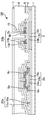
- FIG. 1 is a schematic cross-sectional view illustrating a configuration of a wiring board according to Example 1.
- FIG. 6 is a schematic cross-sectional view showing a configuration of a wiring board according to Comparative Example 1.
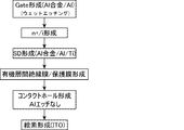
- FIG. 6 is a flowchart of a manufacturing process of the display device substrate according to the first embodiment.
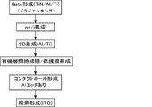
- 10 is a flowchart of a manufacturing process of a display device substrate according to Comparative Example 1.
- FIG. 1 is a schematic cross-sectional view illustrating the configuration of the wiring board according to the first embodiment.
- the wiring substrate according to Example 1 is used as a TFT substrate (active matrix substrate) of a liquid crystal display panel.
- the wiring board according to Example 1 includes a gate wiring 102 a in which an aluminum layer 114 a having a thickness of 100 nm and an aluminum uninium alloy layer 113 a having a thickness of 50 nm are stacked in this order on a substrate 101, and a wiring board having a thickness of 100 nm.
- An intrinsic semiconductor layer 108a that becomes a channel of the thin film transistor and a high-resistance semiconductor layer (i layer) 108b that becomes a part of the drain wiring 120b are disposed thereon.
- An N-type semiconductor layer (n layer) 109a to be a source electrode, an N-type semiconductor layer (n layer) 109c to be a drain electrode, and an N-type semiconductor layer 109b to be a part of the drain wiring 120b are disposed thereon.
- the gate insulating film 104 has a thickness of 410 nm
- the high-resistance semiconductor layers 108a and 108b have a thickness of 175 nm
- the N-type semiconductor layers 109a, 109b, and 109c have a thickness of 55 nm.
- an aluminum alloy layer used for the gate wiring 102a an element such as nickel, iron, cobalt, or the like is added to Al, and boron, neodymium, lanthanum, or the like may be added as an additional element. This is a preferred form. By adding such an additional element, for example, the heat resistance can be improved and the characteristics as a good barrier metal can be exhibited.
- a source wiring 120a in which a titanium layer 110a, an aluminum unilayer 111a, and an aluminum alloy layer 112a are stacked, and a titanium layer 110b, an aluminum unilayer 111b, and an aluminum alloy layer 112b are stacked.
- the drain wiring 120b is arranged.
- the auxiliary capacitance for holding the voltage applied to the liquid crystal is formed by the auxiliary capacitance wiring 103, the gate insulating film 104, and the drain wiring 120b.
- the titanium layer, the aluminum layer, and the aluminum alloy layer provided on the N-type semiconductor layer 109 c serving as the drain electrode are part of the drain wiring 120 b and are identical to the drain wiring 120 b provided on the auxiliary capacitance wiring 103. It is a continuation wiring.
- the aluminum alloy layer 112a constituting the source wiring 120a and the aluminum alloy layer 112b constituting the drain wiring 120b are preferably Al- (0.5 to 5.0) at% Ni.
- iron, cobalt, etc. instead of nickel depending on the situation.
- lanthanum, neodymium, boron, carbon, silicon, and the like may be added as other additive elements.
- the content is preferably, for example, 0.1 to 3.0 at%.
- the titanium layers 110a and 110b have a thickness of 30 nm
- the aluminum layers 111a and 111b have a thickness of 100 nm
- the aluminum alloy layers 112a and 112b have a thickness of 50 nm.
- a protective film 105 and an organic interlayer insulating film 106 made of silicon nitride and having a thickness of 250 nm are disposed on the entire surface of the wiring substrate.
- the semiconductor layer constituting the thin film transistor and the unevenness formed by the source wiring 120a are flattened by the organic interlayer insulating film 106, and a pixel electrode 107 made of indium tin oxide and having a thickness of 90 nm is disposed thereon.
- the pixel electrode 107 is formed separately for each pixel displaying each color, and is formed on the aluminum alloy layer 112b constituting the drain wiring 120b through the contact hole 115 provided in the organic interlayer insulating film 106 and the protective film 105. It is connected.
- the aluminum alloy layer 112b and the pixel electrode 107 can be directly connected, the diameter of the contact hole can be reduced, and the wiring width of the auxiliary capacitance wiring can also be reduced.
- Example 1 the manufacturing method of the wiring board based on Example 1 is demonstrated.
- an aluminum film and an aluminum alloy film are formed on a substrate 101 by a sputtering method or the like, and patterned by wet etching using phosphorous acetic acid or the like, whereby an aluminum layer 114a and an aluminum alloy layer 113a are stacked.
- the auxiliary capacitance wiring 103 in which the aluminum layer 102b and the aluminum layer 114b and the aluminum alloy layer 113b are laminated is formed.
- a silicon nitride film is formed on the gate wiring 102 a and the auxiliary capacitance wiring 103 by a plasma induced chemical vapor deposition (PECVD) method or the like to form a gate insulating film 104.
- PECVD plasma induced chemical vapor deposition
- a high-resistance semiconductor layer having a low impurity concentration and an N-type silicon layer are formed thereon by PECVD or the like, and patterning is performed to form a semiconductor layer 108a serving as a thin film transistor channel, a source electrode, and a drain electrode.
- N-type semiconductor layers 109a and 109c are formed.
- a patterned high-resistance semiconductor layer 108b and an N-type semiconductor layer 109b are formed on the gate insulating film 104 in the region where the auxiliary capacitance wiring 103 is disposed.
- a titanium film, an aluminum film, and an aluminum alloy film are formed by a sputtering method or the like, and patterning is performed, whereby the source wiring 120a in which the titanium layer 110a, the aluminum layer 111a, and the aluminum alloy layer 112a are stacked, and the titanium layer 110b.
- the drain wiring 120b in which the aluminum layer 111b and the aluminum alloy layer 112b are stacked is formed.
- the N-type semiconductor layer is also patterned, so that the N-type semiconductor layer is divided, and N-type semiconductor layers 109a and 109c to be a source electrode and a drain electrode are formed.
- nickel, lanthanum, or the like can be used, and other metal elements may be included.
- a protective film 105 is formed on the entire surface of the substrate using a PECVD method or the like.
- Al 3 Ni crystals are deposited at the interface between the aluminum alloy layer 112a and the protective film 105 by heating to 200 to 300 ° C.
- it is possible to reduce the contact resistance between the transparent conductive film can be prevented that the Al 2 O 3 is formed on the surface of the aluminum alloy can be formed later.
- an organic interlayer insulating film 106 is formed by spin coating or the like, and a contact hole 115 penetrating the protective film 105 and the organic interlayer insulating film 106 is formed so as to expose the surface of the aluminum alloy layer 112b of the drain wiring 120b. . Then, an indium tin oxide film is formed thereon and patterned to form the pixel electrode 107. Thereby, the pixel electrode 107 and the drain 120b whose uppermost layer is the aluminum alloy layer 112b are connected.
- a wiring board formed in this way is bonded to a substrate facing it, and a liquid crystal display panel is manufactured by injecting liquid crystal. Moreover, it becomes a display apparatus by providing a polarizing plate and another member in this display panel.
- the wiring structure of the present invention in which an aluminum alloy layer and other layers are laminated can be used for other than source wiring, drain wiring, and gate wiring.
- the wiring structure of the present invention has a sensor function. When used in a panel, the wiring structure of the present invention can also be used for a photosensor wiring or the like.
- the gate wiring 102a, the gate insulating film 104, and the semiconductor layer 105 are formed in this order from the substrate 101 side, and the back gate type thin film transistor in which the source electrode 109a and the source wiring 120a are connected is formed.
- This wiring structure can be suitably used also in a top gate type thin film transistor.
- the gate wiring may include an Al alloy / Al laminated structure
- the source wiring and the auxiliary capacitance wiring may include an Al alloy / Al laminated structure.
- Example 1 a wiring structure in which an aluminum alloy layer and an aluminum layer are laminated is formed.
- aluminum is used.
- An aluminum alloy layer added with a transition metal element such as nickel can be suitably used as a combination of additive elements, but other transition metal elements (iron, cobalt, etc.) and additive elements such as carbon, silicon, boron, etc. May be appropriately selected depending on the characteristics required.
- the combination of the type of additive element and another conductive layer such as an aluminum layer may be set as appropriate.
- the source wiring and the drain wiring are a three-layer wiring structure in which a titanium layer, an aluminum layer, and an aluminum alloy layer are formed in this order, but an aluminum alloy layer is used instead of the titanium layer.
- the three-layer structure used may be used and is not limited.
- FIG. 2 is a schematic cross-sectional view illustrating a configuration of a wiring board according to Comparative Example 1.
- the gate wiring 2a has a structure in which a titanium layer 15a, an aluminum layer 14a, and a titanium nitride layer 13a are stacked, and the auxiliary capacitance wiring 3 has a titanium layer 15b.
- the aluminum layer 14b and the titanium nitride layer 13b are stacked.
- the source wiring 20a has a structure in which a titanium layer 10a and an aluminum layer 11a are stacked from the substrate side
- the drain wiring 20b has a structure in which a titanium layer 10b and an aluminum layer 11b are stacked.
- the thin film transistor includes a gate wiring 2a, a gate insulating film 4, a high resistance semiconductor layer 8a, high resistance semiconductor layers 9a and 9c serving as a source electrode and a drain electrode, and a source wiring 20a arranged in this order.
- a protective film 5 and an organic interlayer insulating film 6 are disposed on the thin film transistor and the auxiliary capacitor, and a pixel electrode 7 is disposed thereon. The pixel electrode 7 is in contact with the gate insulating film 4 through a contact hole 15 formed in the protective film 5, the organic interlayer insulating film 6, and the drain wiring 20b.
- the drain wiring 20b and the pixel electrode 7 are connected, but the drain wiring 20b is formed in the same process as the titanium layer and the aluminum layer formed on the N-type semiconductor layer 9c to be the drain electrode. It is a continuous wiring.
- a method for manufacturing a wiring board according to Comparative Example 1 will be described.
- a titanium film having a thickness of 30 nm, an aluminum film having a thickness of 50 nm, and a titanium nitride film having a thickness of 100 nm are formed on the substrate 1 by sputtering or the like, and plasma etching (PE) or reactive ion etching (Reacting Ion Etching) is performed.
- PE plasma etching
- Reacting Ion Etching reactive ion Etching
- RIE reactive ion etching
- a silicon nitride film is formed on the gate wiring 2 a and the auxiliary capacitance wiring 3 by a PECVD method or the like to form a gate insulating film 4. Further, a high-resistance semiconductor layer and an N-type semiconductor layer are formed thereon in this order, and patterning is performed, so that a high-resistance semiconductor layer 8a serving as a channel of the thin film transistor and an N-type semiconductor layer 9a serving as a source electrode and a drain electrode are formed. And 9c are formed. Further, a patterned high-resistance semiconductor layer 8b and N-type semiconductor layer 9b are formed on the gate insulating film 4 in the region where the auxiliary capacitance wiring 3 is disposed.
- a titanium film is formed by sputtering or the like and patterned.
- a source wiring 20a in which the titanium layer 10a and the aluminum layer 11a are stacked, and a drain wiring 20b in which the titanium layer 10b and the aluminum layer 11b are stacked are formed.
- N-type semiconductor layers 9a, 9b, and 9c to be a source electrode and a drain electrode are formed by patterning the N-type semiconductor layer at the same time.
- a protective film 5 is formed on the entire surface of the substrate using a PECVD method or the like, and an organic interlayer insulating film 6 is formed using a spin coating method or the like. Thereafter, a contact hole 15 penetrating the protective film 5 and the organic interlayer insulating film 6 is formed in a region where the drain wiring 20b is disposed. At this time, a part of the aluminum layer 11b is etched to expose a part of the surface of the titanium layer 10b. Thereafter, an indium tin oxide film is formed and patterned to form the pixel electrode 7. Thereby, the pixel electrode 7 and the drain wiring 20b are connected.
- the contact resistance may be increased due to the formation of an oxide film. Therefore, the titanium layer 10b disposed below the aluminum layer 11b and the pixel electrode 7 are connected. is doing.
- FIG. 3 is a manufacturing flowchart of the wiring board according to the first embodiment
- FIG. 4 is a manufacturing flowchart of the wiring board according to the first comparative example.
- the gate wiring has an Al alloy / Al laminated structure (two-layer structure), and in Comparative Example 1, a TiN / Al / Ti laminated structure (three layers). Structure).
- patterning of the gate wiring can be performed by wet etching using phosphorous acetic acid or the like.
- etching is collectively performed by wet etching.
- the gate wiring is patterned by dry etching. Wet etching is less expensive than dry etching, and the manufacturing cost can be reduced by using an Al alloy / Al laminated structure.
- a single layer made of only an Al alloy may be used as the gate wiring in order to reduce the type of material.
- Example 1 and Comparative Example 1 a contact hole is formed after the organic interlayer insulating film and the protective film are formed, and the pixel electrode and the drain wiring are connected.
- Comparative Example 1 in order to connect the titanium layer 10b and the pixel electrode 7, a step of removing a part of the aluminum layer 11b formed on the titanium layer 10b by etching is required. Since the aluminum alloy layer 111b that forms the uppermost layer of the drain wiring 120b can be connected to the pixel electrode 107, it is not necessary to etch the aluminum layer, and the number of manufacturing steps can be reduced.
- Comparative Example 1 the aluminum layer is etched so that a part of the upper surface of the titanium layer is exposed. Therefore, in order to cover the product yield due to etching failure, it is necessary to increase the diameter of the contact hole. is there.
- Example 1 since it can connect with the uppermost aluminum alloy layer, a contact hole diameter can be made small. As a result, the width of the auxiliary capacitance wiring can be narrowed, and the aperture ratio of the picture element can be increased.
Landscapes
- Physics & Mathematics (AREA)
- Nonlinear Science (AREA)
- Mathematical Physics (AREA)
- Engineering & Computer Science (AREA)
- Chemical & Material Sciences (AREA)
- Crystallography & Structural Chemistry (AREA)
- Microelectronics & Electronic Packaging (AREA)
- General Physics & Mathematics (AREA)
- Optics & Photonics (AREA)
- Internal Circuitry In Semiconductor Integrated Circuit Devices (AREA)
- Thin Film Transistor (AREA)
- Electrodes Of Semiconductors (AREA)
- Devices For Indicating Variable Information By Combining Individual Elements (AREA)
Abstract
本発明は、酸化物電極との良好な接続を行うことや、絶縁膜等との界面で生じる相互拡散を抑制することができ、かつ製造工程の低コスト化を図ることができる配線構造体、それを用いた半導体素子、配線基板、表示用パネル及び表示装置を提供する。本発明の配線構造体は、アルミニウム層、銅層及び銅合金層からなる群より選択される少なくとも1つの層と、アルミニウム合金層とを含む2層以上の積層体であり、該アルミニウム合金層が表層に配置されている配線構造体である。
Description
本発明は、配線構造体、半導体素子、配線基板、表示用パネル及び表示装置に関する。より詳しくは、透明導電膜を有する表示装置等に好適に用いることができる配線構造体、それを備える半導体素子、配線基板、表示用パネル及び表示装置に関するものである。
配線構造体は、電気信号や電力を伝達する導体として電子・電気部品に用いられており、例えば、プリント配線板、半導体装置、表示装置用のアクティブマトリクス基板等において回路や半導体素子を構成するものである。
配線構造体には、低抵抗であり、更に、該配線構造体に接続される電極や半導体との接触抵抗が低い金属材料が好ましく用いられるが、中でも、アルミニウムは高い導電性を有するため、特に好ましく用いられている金属材料の一つである。
しかしながら、アルミニウム等の金属は酸化しやすい金属であるため、導電性酸化物と接続するような場合に、その接続界面に強固な酸化膜が形成され、電気を通すことができなくなることがあった。例えば、液晶表示装置、有機エレクトロルミネッセンス(有機EL)表示装置等の表示装置においては透明導電膜が用いられ、この透明導電膜としては酸化インジウム錫(ITO:Indium Tin Oxide)が表示用の絵素電極として用いられているが、アルミニウム層と絵素電極とを直接接続すると酸化アルミニウムの生成により、接続部分の抵抗が高くなるおそれがあった。また、加熱により絶縁膜等との界面で相互拡散が生じ、その特性を劣化させるおそれがあった。
そのため、従来の液晶表示装置においては、配線構造体として、アルミニウム層と、窒化チタン膜、チタン膜、モリブデン膜等のバリアメタル層とを用いることで、酸化物電極と配線構造体との界面における酸化膜の形成を抑制したり、配線が接する絶縁膜等との界面における相互拡散を抑制していた。このような場合、アルミニウム層を形成するとともに、チタン膜等を形成することとなるため、生産性の向上、低コスト化を実現することができる配線構造体が求められるところであった。
このような中で、液晶表示装置等に用いられる半導体素子として、例えば、半導体層と電極層とが直接接合される部分を有しており、該電極層は、ニッケル、コバルト、鉄などの遷移金属を含有したアルミニウム合金薄膜で形成されている半導体素子が開示されている(例えば、特許文献1参照。)。ここでは、アルミニウム合金薄膜の単層配線を薄膜トランジスタの半導体層と接続しているが、この半導体層を構成するシリコンと電極層を構成する元素との相互拡散を抑制することを目的とするものである。
また、炭素を含有したアルミニウム合金薄膜において、ニッケル、コバルト、鉄のうち少なくとも1種以上の元素を0.5~7.0at%と、炭素を0.1~3.0at%とを含有し、残部がアルミニウムであるアルミニウム合金薄膜が開示されている(例えば、特許文献2参照。)。更に、ガラス基板上に配置された薄膜トランジスタと、透明電極によって形成された画素電極、および、これら薄膜トランジスタと画素電極を電気的に接続するアルミニウム合金膜を有し、該アルミニウム合金膜と前記画素電極は、Mo、Cr、Ti、Wからなる高融点金属を介さずに直接接続しており、前記アルミニウム合金膜と画素電極が直接接触した接触界面において、前記アルミニウム合金膜を構成する合金成分の一部または全部が、析出物もしくは濃化層として存在している表示デバイスが開示されている(例えば、特許文献3参照。)。
しかしながら、従来のアルミニウム合金を用いた配線は、アルミニウム合金薄膜を単層配線として用いている。このような場合、充分な導電性を有するためには、アルミニウム合金薄膜を厚く形成する必要があるが、アルミニウム合金は、単体アルミニウムと比較して高値であるため、低コスト化を図るためには更なる改善の余地があり、酸化物電極や絶縁膜等との界面における状態を良好なものとするとともに、低コスト化が望まれていた。
本発明は、上記現状に鑑みてなされたものであり、酸化物電極等との良好な接続を行うことができ、かつ低コスト化を図ることができる配線構造体を提供することを目的とするものである。
本発明者らは、酸化物電極と接続したとしても接触抵抗を低くすることができ、更には、低コスト化を図ることができる配線構造体について種々検討したところ、アルミニウム合金層を用いることに着目した。そして、アルミニウム合金単層で配線を形成した場合にはコストが高くなることや、アルミニウム合金層とチタン層とを積層させた構造の場合にはチタン層中にアルミニウム合金中の元素が拡散し、配線の特性を劣化させることを見出した。そして、アルミニウム層、銅層及び銅合金層からなる群より選択される少なくとも1つの層と、アルミニウム合金層とを含む2層以上の積層体であり、該アルミニウム合金層が表層に配置された配線構造体であることによって、例えば、アルミニウム合金層で酸化物電極と接続し、低抵抗のコンタクトをとることができる。また、例えば、配線構造体が接する絶縁膜等との界面における相互拡散を抑制することができる。更には、酸化物電極等と接触する表層のみをアルミニウム合金層とすることで、アルミニウム合金単層を配線として用いる場合よりもアルミニウム合金の使用量を低減することができ、これにより、低コスト化及び他の電極等との良好な接続を実現することができることを見いだし、上記課題をみごとに解決することができることに想到し、本発明に到達したものである。
すなわち、本発明は、アルミニウム層、銅層及び銅合金層からなる群より選択される少なくとも1つの層と、アルミニウム合金層とを含む2層以上の積層体であり、該アルミニウム合金層が表層に配置されている配線構造体である。
以下に本発明を詳述する。
以下に本発明を詳述する。
本発明の配線構造体は、アルミニウム層、銅層及び銅合金層からなる群より選択される少なくとも1つの層と、アルミニウム合金層とを含む2層以上の積層体であり、アルミニウム合金層が表層に配置されている。すなわち、アルミニウム層、銅層及び銅合金層からなる群より選択される少なくとも1つの層を含む配線構造体において、少なくとも一方の面側にアルミニウム合金層が配置されているものである。この場合、アルミニウム合金層の表面が露出した形態で配置されることになる。アルミニウム層、銅層、銅合金層は、電気電導性に優れ、また、比較的安価である点で、種々の電気・電子機器において配線を形成する金属材料として好ましく用いられている。しかしながら、アルミニウム、銅、銅合金等は酸化しやすく、例えば、酸化物電極等と接続させると接触部分に酸化膜(例えば、酸化アルミニウムや酸化銅)が形成し、電気伝導性を妨げることがあった。また、絶縁膜等との界面で配線構造体を構成する元素と、絶縁膜を構成する元素との相互拡散が生じることがあった。本発明の配線構造体では、表層に設けられたアルミニウム合金層と酸化物電極とを接続することができるため、酸化膜の生成を抑制し、接触抵抗を低下させることができる。また、アルミニウム合金層がバリアメタル層として機能することによって、相互拡散を抑制することができる。このような形態において、アルミニウム合金層を表層に設ける効果がより発揮される。更に、アルミニウム層、銅層、銅合金層等は比較的安価であり、電気電導性にも優れるため、良好な特性の配線構造体を安価に形成することができる。
上記アルミニウム合金層は、配線構造体の少なくとも一方の面側の表層に設けられていればよく、配線構造体を形成する他の層には安価なアルミニウム層、銅層、銅合金層や、必要に応じて他の導電層を用いることができる。そのため、配線構造体の導電性を高めるとともに、高値のアルミニウム合金の使用量を低減し、低コスト化を図ることができる。
上記配線構造体は、アルミニウム合金層を含む2層以上が接して配置された構造を有するものであればよく、3層以上であってもよい。
上記アルミニウム合金層は、配線構造体の一方の面側の全面に設けられていてもよいし、配線構造体の一方の面側の一部に設けられていてもよい。例えば、配線構造体と酸化物電極とが接続される場合、少なくとも酸化物電極と接続する部分にアルミニウム合金層が配置されていれば、配線構造体と酸化物電極との接触抵抗を低減することができる。他の部材(例えば、絶縁膜等)との界面で相互拡散が生じることを抑制する観点からは、配線構造体の一方の面側の全面にアルミニウム合金層が配置されている形態が好ましい。
上記アルミニウム合金層は、アルミニウムを主成分とする合金であり、例えば、アルミニウムと他の金属元素、又は、アルミニウムと炭素、窒素、ケイ素等の非金属元素との合金である。アルミニウム合金層を構成するアルミニウム以外の元素(以下では、「添加元素」ともいう。)は、1種でもよいし、2種以上でもよい。
上記アルミニウム合金層の組成は、合金とするために添加される元素の種類等によって適宜設定されるが、例えば、アルミニウムの含有量が50.0at%以上、99.5at%以下であることが好ましい。すなわち、アルミニウム合金に添加される元素は、0.5at%を超えることが好ましく、また、50.0at%未満であることが好ましい。これにより、アルミニウムとしての優れた電気伝導性等を保ちつつ、合金としての特性を有効に発揮することができる。例えば、酸化物電極との接触抵抗を充分に低減することや、接触界面での相互拡散を抑制することができる。
なお、アルミニウム合金の組成については、例えば、オージェ電子分光分析や蛍光X線EDX、ICP-MS(誘導結合プラズマ質量分析)によって測定することができる。アルミニウム合金に添加された添加元素や、銅合金の組成についても、同様の方法によって測定することができる。
なお、アルミニウム合金の組成については、例えば、オージェ電子分光分析や蛍光X線EDX、ICP-MS(誘導結合プラズマ質量分析)によって測定することができる。アルミニウム合金に添加された添加元素や、銅合金の組成についても、同様の方法によって測定することができる。
上記アルミニウム合金層は、配線構造体の1/2以下の厚みであることが好ましい。このような形態では、アルミニウム合金層は配線構造体の表層に薄膜として設けられることになる。アルミニウム合金層は、酸化物電極等の電極層との接触部分に設けられていれば、その特性を充分に発揮することができるが、アルミニウム合金は高値であるため、使用量を低減することが好ましい。そこで、配線構造体の上層の薄膜だけにアルミニウム合金を使用することで、配線をアルミニウム合金単層膜で形成する場合と比較してコストを低減することができる。より好ましい形態としては、アルミニウム合金層は、アルミニウム合金層以外の他の層(他の層が複数ある場合には、複数の層の合計)の半分以下(1/2以下)の厚みであることが好ましい。また、アルミニウム合金層としての特性を充分に発揮するためには、厚みが10nm以上であることが好ましい。このような厚みであることにより、酸化物電極等との接続を行った場合にも、接触抵抗を良好なものとするとともに、製造コストの削減を図ることができる。
上記表層に配置されたアルミニウム合金層は、アルミニウム合金層以外の他の導電層(アルミニウム層、銅層、銅合金層等)が配置された面とは反対側の面に、アルミニウム合金を形成する添加元素とアルミニウムとの結晶が析出したものであることが好ましい。このような形態では、酸化アルミニウムが生成することを抑制することができ、アルミニウム合金層と酸化物電極とを接続させた場合にも、接触抵抗を低くすることができる。アルミニウム合金は、熱処理等が行われることによって、アルミニウム合金の表面に添加元素が拡散し、アルミニウムと添加元素との結晶が析出する。例えば、アルミニウム合金がNi元素を含むものである場合には、Al3Ni結晶が表面に析出されることとなり、これにより、酸化膜の形成を抑制することができる。熱処理の温度は、アルミニウム合金に添加される元素の種類や量によって適宜設定されればよいが、例えば、200~400℃であることが好ましい。
上記配線構造体は、アルミニウム層を含むことが好ましい。すなわち、アルミニウム合金層とアルミニウム層とを含む配線構造体であることが好ましい。アルミニウム合金層とアルミニウム層とが積層された形態である場合には、配線構造体を形成する2層のパターニングを、ウェットエッチングにより一括して行うことができる。例えば、チタン層等を含む配線構造体である場合には、該チタン層のパターニングにはドライエッチングを用いることが好ましいが、製造コスト削減の観点からは、ウェットエッチングを用いてパターニングすることが好適である。なお、アルミニウム層及びアルミニウム合金層は、それぞれ1層で設けられていてもよいし、2層以上で設けられていてもよい。例えば、上記配線構造体の構造としては、Al合金/Al/Al合金の3層構造等も考えられる。アルミニウム合金層は、酸化物電極や、シリコン等の半導体層との接続を良好なものとすることができるため、このような構造では、一方の表面で酸化物電極と接続し、もう一方の表面では半導体層との接続を行うこともできる。
以下に、アルミニウム層等のアルミニウム合金層以外の層について説明する。
上記アルミニウム層は、実質的にアルミニウム金属のみで構成されている層である。アルミウニム層を含む配線構造体の製造においては、アルミニウム層と接触する他の金属材料や層間絶縁膜等から元素が拡散することもあるため、微量の不純物元素が含まれている場合もある。
上記アルミニウム層は、実質的にアルミニウム金属のみで構成されている層である。アルミウニム層を含む配線構造体の製造においては、アルミニウム層と接触する他の金属材料や層間絶縁膜等から元素が拡散することもあるため、微量の不純物元素が含まれている場合もある。
上記アルミニウム層及びアルミニウム合金層は、燐硝酢酸等を用いたウェットエッチングによって一括してパターニングを行うことができるため、ドライエッチングによりパターニングを行う場合と比較して、製造工程を安価なものとすることができる。例えば、配線構造体にチタン層を用いる場合には、ウェットエッチングではパターニングすることが難しく、通常、ドライエッチングを用いることとなる。このような観点からは、上記配線構造体は、アルミニウム層及びアルミニウム合金層を含むものであることが好ましい形態である。
上記銅層は、実質的に銅のみで構成されている層である。銅層を含む配線構造体の製造においては、銅層と接触する他の金属材料や層間絶縁膜等から元素が拡散することもあるため、微量の不純物元素が含まれている場合もある。
上記銅合金層は、銅を必須として含み、更に他の金属元素や、炭素、ケイ素等の非金属元素を含んで構成されるものである。銅合金層中の他の元素の種類や量は特に限定されないが、銅合金層中の銅元素は50at%以上であることが好ましく、99.5at%以下であることが好ましい。銅合金に添加される元素としては、例えば、Mg、Mn等が挙げられるが、特に限定されるものではなく、配線構造体を用いる用途等によって適宜設定すればよい。
上記銅合金層は、銅を必須として含み、更に他の金属元素や、炭素、ケイ素等の非金属元素を含んで構成されるものである。銅合金層中の他の元素の種類や量は特に限定されないが、銅合金層中の銅元素は50at%以上であることが好ましく、99.5at%以下であることが好ましい。銅合金に添加される元素としては、例えば、Mg、Mn等が挙げられるが、特に限定されるものではなく、配線構造体を用いる用途等によって適宜設定すればよい。
上記配線構造体は、シリコン等からなる半導体膜と接続する観点からも好適である。これによれば、配線構造体中の金属元素が半導体膜中に拡散することを抑制することができるため、良好なオーミック特性を得ることができる。例えば、アルミニウム膜とシリコン膜とを接続して加熱を行った場合には、アルミニウム膜とシリコン膜との界面付近で相互拡散が生じるおそれがある。シリコン膜との接続をアルミニウム合金層で行うことにより、その界面にアルミニウム合金層を構成する元素(例えば、ニッケル等)と、シリコンとの反応層が形成され、これにより、相互拡散を抑制することができる。
上記配線構造体は、電子機器等を構成する配線として用いられ、導電層が積層された構造を有するものである。配線は、電気信号を伝達する信号配線、電源を供給するための電源配線、回路を構成する配線、電界を印可する(例えば、TFTのゲートに電界を印可する)ための配線等であり、特に限定されるものではない。例えば、薄膜トランジスタ(TFT)においては、ソース・ドレイン配線、ゲート配線等が挙げられ、本明細書中では、ゲート配線のように信号が伝達されるとともに、ゲート絶縁膜等に電界を印可する部分についても「配線」に含めるものとする。また、本発明の配線構造体を備える配線基板を用いた液晶表示装置の場合には、液晶に印可した電圧を保持するために用いられる補助容量を形成する補助容量配線であることも好ましい。更に、例えば、光センサーを有する電子機器に本発明の配線構造体を用いる場合には、光センサー用配線であることも好ましい形態である。
本発明の配線構造体における好ましい形態について以下に詳しく説明する。
上記アルミニウム合金層は、遷移金属元素を含むことが好ましい。遷移金属元素は、周期表の第3族から第11族の元素である。遷移金属元素は、d軌道又はf軌道が閉殻でない金属元素であるが、アルミニウムとの結晶がアルミニウム合金層の表面に析出しやすくなり、アルミニウム合金層の表層に酸化膜が形成されることをより抑制することができたり、アルミニウム合金層の耐熱性を向上させることによって、他の部材との界面で生じる相互拡散を抑制することができる。遷移金属元素としては、特に限定されるものではなく、例えば、ニッケル、鉄、コバルト、チタニウム、バナジウム、クロム、ジルコニウム、ニオブ、モリブデン、ルテニウム、ロジウム、パラジウム、ハフニウム、タンタル、タングステン、オスミウム、イリジウム、白金等や、ランタノイド、アクチノイド等の種々の金属元素を挙げることができる。また、酸化物電極等との接触抵抗を低減する観点からは、上記アルミニウム合金層は、鉄、コバルト及びニッケルからなる群より選択される少なくとも1つを含むことが好ましい。鉄、コバルト及びニッケルは鉄族元素とも呼ばれ、類似した性質を有する。ニッケル等の元素は、加熱等によってアルミニウム合金層の表面に金属結晶を析出しやすく、酸化物電極との界面に酸化アルミニウムが生成することを防止することができ、接触抵抗を低減することができる。絶縁膜等の他の層との界面で相互拡散が生じることを抑制する観点からは、ネオジウム及びランタンの少なくとも1つを含むことが好ましい。これらの酸化物電極との界面に酸化膜を形成することができる元素と、耐熱性を向上させることで相互拡散を抑制することができる元素を併用することによって、より好ましい配線構造体の形態とすることができる。
アルミニウム合金層が遷移金属元素を含む場合、アルミニウム合金層中の遷移金属元素の含有割合は、0.5at%以上、50at%未満であることが好ましい。より好ましくは、0.5~10.0at%である。また、酸化物電極等との接触抵抗を低減する観点から、鉄、コバルト及びニッケルの中から元素を添加する場合、その含有量は、0.5~5.0at%であることが好ましい。絶縁膜等との界面において生じる相互拡散を抑制するために、ネオジウム、ランタン等を用いる場合、該ネオジウム、ランタン等の含有量は、0.1~3.0at%であることが好ましい。
上記アルミニウム合金層は、遷移金属元素を含むことが好ましい。遷移金属元素は、周期表の第3族から第11族の元素である。遷移金属元素は、d軌道又はf軌道が閉殻でない金属元素であるが、アルミニウムとの結晶がアルミニウム合金層の表面に析出しやすくなり、アルミニウム合金層の表層に酸化膜が形成されることをより抑制することができたり、アルミニウム合金層の耐熱性を向上させることによって、他の部材との界面で生じる相互拡散を抑制することができる。遷移金属元素としては、特に限定されるものではなく、例えば、ニッケル、鉄、コバルト、チタニウム、バナジウム、クロム、ジルコニウム、ニオブ、モリブデン、ルテニウム、ロジウム、パラジウム、ハフニウム、タンタル、タングステン、オスミウム、イリジウム、白金等や、ランタノイド、アクチノイド等の種々の金属元素を挙げることができる。また、酸化物電極等との接触抵抗を低減する観点からは、上記アルミニウム合金層は、鉄、コバルト及びニッケルからなる群より選択される少なくとも1つを含むことが好ましい。鉄、コバルト及びニッケルは鉄族元素とも呼ばれ、類似した性質を有する。ニッケル等の元素は、加熱等によってアルミニウム合金層の表面に金属結晶を析出しやすく、酸化物電極との界面に酸化アルミニウムが生成することを防止することができ、接触抵抗を低減することができる。絶縁膜等の他の層との界面で相互拡散が生じることを抑制する観点からは、ネオジウム及びランタンの少なくとも1つを含むことが好ましい。これらの酸化物電極との界面に酸化膜を形成することができる元素と、耐熱性を向上させることで相互拡散を抑制することができる元素を併用することによって、より好ましい配線構造体の形態とすることができる。
アルミニウム合金層が遷移金属元素を含む場合、アルミニウム合金層中の遷移金属元素の含有割合は、0.5at%以上、50at%未満であることが好ましい。より好ましくは、0.5~10.0at%である。また、酸化物電極等との接触抵抗を低減する観点から、鉄、コバルト及びニッケルの中から元素を添加する場合、その含有量は、0.5~5.0at%であることが好ましい。絶縁膜等との界面において生じる相互拡散を抑制するために、ネオジウム、ランタン等を用いる場合、該ネオジウム、ランタン等の含有量は、0.1~3.0at%であることが好ましい。
上記アルミニウム合金層は、周期表の第13族元素及び第14族元素からなる群より選択される少なくとも1つの元素を含むことが好ましい。周期表の第13族元素としては、ボロン、ガリウム、インジウム等が挙げられる。また、周期表の第14族元素としては、炭素、ケイ素、ゲルマニウム、錫、鉛等が挙げられる。このような元素は、アルミニウム合金の耐熱性を向上させる点や、アルミニウム元素と良好な合金を形成しやすい点で好ましい。これらの元素の中でも、ボロン、炭素、ケイ素が好ましい添加元素として挙げられる。このような添加元素は、遷移金属元素とともに添加されてもよいし、単体で添加されてもよいし、特に限定されない。周期表の第13族元素及び第14族元素の含有量として好ましい範囲としては特に限定されないが、例えば、0.1~5.0at%であることが好ましい。
上記配線構造体は、アルミニウム層、銅層及び銅合金層からなる群より選択される少なくとも1つの層と、アルミニウム合金層とを含むものであるが、アルミニウム合金層中の添加元素と、他の導電層との種類や、その組み合わせについては特に限定されるものではなく、用いられる用途等によって適宜設定されればよい。例えば、ニッケルを添加元素として含むアルミニウム合金層と、アルミニウム層とを含む配線構造体であってもよいし、ケイ素を添加元素として含むアルミニウム合金層と、銅層とを含む配線構造体であってもよいし、特に限定されるものではない。
上記配線構造体の好ましい形態としては、3層以上の積層体であり、アルミニウム合金層が両表層に配置されている形態が挙げられる。すなわち、上記配線は、アルミニウム層、銅層、銅合金層等の他の導電層を挟んで、アルミニウム合金層が配線構造体の両面に設けられていることが好ましい。このように、両面にアルミニウム合金層を配置することで、配線構造体の両面のいずれにおいても酸化物電極やシリコン等の半導体層との接続を良好なものとすることができる。また、絶縁膜等との界面でアルミニウム等の元素が拡散することを防止することができ、例えば、配線構造体をTFTのソース電極等として用いた場合には、そのトランジスタ特性を良好なものとすることができる。
上記配線構造体の好ましい形態としては、3層以上の積層体であり、一方の面にはアルミニウム合金層が設けられ、反対側の面には、チタン層又はモリブデン層が積層されている形態が挙げられる。例えば、上記配線構造体がアルミニウム層を含む場合には、アルミニウム合金層、アルミニウム層及びチタン層がこの順に積層された構造、又は、アルミニウム合金層、アルミニウム層及びモリブデン層がこの順に積層された構造であることが好ましい。このように、アルミニウム合金層と、チタン層又はモリブデン層との間にアルミニウム層を介在させる、すなわち、アルミニウム層等を中間層として用いる場合、チタン層又はモリブデン層にアルミニウム合金層中の添加元素が拡散することを抑制することができる。これによれば、配線の特性を良好なものとすることができ、例えば、該配線をTFTのソース電極等として用いた場合には、そのトランジスタ特性を良好なものとすることができる。これは、アルミニウム層を銅層、銅合金層と置き換えてもよく、特に限定されるものではない。
上記配線構造体の好ましい形態としては、アルミニウム合金層が配置された面とは反対側に、チタン層が積層されている形態が挙げられる。モリブデンは、チタンよりも水等によって劣化しやすい金属材料であるため、安定性の観点からは、モリブデン層よりもチタン層を用いることが好ましい。
上記配線構造体の好ましい形態としては、アルミニウム合金層が配置された面とは反対側に、モリブデン層が積層されている形態が挙げられる。モリブデン層は、アルミニウムと同じエッチング溶液を用いることでパターニングすることができるため、アルミニウム及びアルミニウム合金と一括してパターニングを行うことができる。そのため、配線構造体が用いられる用途によっては、モリブデンを用いることで製造工程を簡略化するこができ、生産性の向上を図ることができる。
本発明はまた、上記配線構造体と半導体層とを含む半導体素子でもある。半導体素子と電気的に接続される配線として上記配線構造体を用いることによって、上記配線構造体と他の電極層等との接触抵抗を低減することができ、半導体素子の特性を良好なものとすることができる。半導体素子としては、特に限定されないが、例えば、ダイオード等の2端子素子、トランジスタ等の3端子素子が挙げられる。
上記半導体素子は、薄膜トランジスタ(TFT:Thin Film Transister)であり、上記配線構造体は、ソース・ドレイン配線(ソース配線及び/又はドレイン配線)であることが好ましい。例えば、表示装置用のアクティブマトリクス基板に、上記配線構造体を用いたTFTを用いた場合、TFTのドレイン領域と電気的に接続されたソース・ドレイン配線は、表示画素を構成する絵素電極と接続される。絵素電極には、酸化インジウム錫、酸化インジウム亜鉛等の酸化物電極が用いられているため、上記配線構造体のアルミニウム合金層と酸化物電極とを接続することで、接触抵抗を低減することができる。ソース・ドレイン配線として用いる場合には、アルミニウム合金の添加元素としては、ニッケル、鉄、コバルト等であることが特に好ましい。例えば、ニッケルを含むアルミニウム合金であることによって、加熱処理等によってAl3Niの結晶が析出し、酸化物電極との界面で酸化膜が形成されることを抑制することができる。
上記半導体素子は、薄膜トランジスタであり、上記配線構造体は、ゲート配線であることが好ましい。これによれば、アルミニウム合金層がバリアメタル層の役割を果たすこととなり、アルミニウム層への元素の拡散を抑制することができる。また、バリアメタル層としては、チタン、窒化チタン(TiN)等が用いられているが、これをエッチングする際には、ドライエッチングを行うこととなる。しかしながら、アルミニウム合金層はウェットエッチングによってパターニングすることができるため、ドライエッチングを用いる場合と比較して、コスト削減を図ることができる。
ゲート配線として用いる場合には、端子腐食が問題となるため、アルミニウム合金には耐腐食性や耐熱性が望まれる。アルミニウム合金の添加元素としては、鉄、ニッケル、コバルト等の遷移金属元素を含むことが好ましく、更に、耐熱性等を向上させるために追加元素を添加してもよい。追加元素としては、例えば、ネオジウム、ランタン等が好ましく例示される。ネオジウム等の添加元素を含むことによって、アルミニウム合金層の耐熱性が向上し、配線構造体が接する他の部材との界面で元素の相互拡散が生じることを抑制することができる。
ゲート配線として用いる場合には、端子腐食が問題となるため、アルミニウム合金には耐腐食性や耐熱性が望まれる。アルミニウム合金の添加元素としては、鉄、ニッケル、コバルト等の遷移金属元素を含むことが好ましく、更に、耐熱性等を向上させるために追加元素を添加してもよい。追加元素としては、例えば、ネオジウム、ランタン等が好ましく例示される。ネオジウム等の添加元素を含むことによって、アルミニウム合金層の耐熱性が向上し、配線構造体が接する他の部材との界面で元素の相互拡散が生じることを抑制することができる。
上記配線構造体が液晶表示装置の表示装置用基板に用いられる場合、上記配線構造体は、補助容量配線であることが好ましい。補助容量配線は、液晶に印加される電圧を保持するための補助容量を構成するための配線である。補助容量は、絶縁膜を挟んだ2つの導電層によって容量を形成することによって形成される。そして、この補助容量を構成する導電層(補助容量配線)の一方は絵素電極と接続されるものとなる。補助容量配線を形成する場合、絵素の開口率を大きくするためには補助容量配線の幅を小さくすることが好ましく、例えば、図1に示すような場合、ドレイン配線の一部が補助容量配線の一方として機能することとなるが、ドレイン配線120bと絵素電極107とを接続する場合、ドレイン配線120bの最上層をアルミニウム合金層112bで形成することによって、ドレイン配線120bと絵素電極107とを直接接続することができる。そのため、コンタクトホールの径を小さくすることができ、開口率を大きくすることができる。
例えば、図2に示すように、チタン層10b上にアルミニウム層11bを積層させた構造に対して、その上に形成した保護膜5及び層間有機絶縁膜6にコンタクトホール15を設けて、層間有機絶縁膜6上に形成した絵素電極7とソース配線20aとを接続する場合、アルミニウム層11bと絵素電極7とを直接接続させるとその界面に酸化膜が形成する。そのため、アルミニウム層11bをエッチングしてチタン層10bの表面を露出させるエッチング工程を行い、チタン層と接続させることとなる。そのため、製造工程数の増加により生産性が阻害されるとともに、エッチング不良による製品の収率(製造歩留り)を低下させることとなる。また、コンタクトホール径を大きくすることで、絵素電極と補助容量配線としても機能しているドレイン配線との接触を良好なものとすると、これと接続する配線幅も大きくなるため、絵素の開口率が低下することとなる。
本発明は更に、基板上に、上記配線構造体、絶縁膜及び導電膜がこの順に配置された配線基板であって、該配線構造体は、絶縁膜に設けられたコンタクトホールを介してアルミニウム合金層側から導電膜と接続している配線基板でもある。これによれば、配線構造体の導電膜側にアルミニウム合金層が配置され、該導電膜とアルミニウム合金層とが接続され、接触抵抗を低減することができる。これにより、配線基板の動作をより安定化することができる。
上記基板は、特に限定されるものではなく、種々の基板を用いることができる。例えば、単結晶半導体基板、酸化物単結晶基板、金属基板、ガラス基板、石英基板、樹脂基板等の基板を用いることができる。例えば、単結晶半導体基板や、金属基板等の導電性基板である場合には、その上に絶縁膜等を設けることによって用いることが好ましい。
上記配線構造体と導電膜との間には、絶縁膜が設けられるが、該絶縁膜は1層でもよいし、2層以上でもよい。2層以上である場合には、その2層の絶縁膜を貫通するコンタクトホールが設けられ、配線構造体と導電膜が接続されることとなる。また、絶縁膜を構成する材料は特に限定されず、酸化シリコン、窒化シリコン、有機絶縁材料等の種々の絶縁材料を用いることができる。
上記導電膜は、酸化物電極であることが好ましい。これによれば、配線構造体の酸化物電極側にアルミニウム合金層が配置され、該酸化物電極とアルミニウム合金層とが接続されるため、アルミニウム合金層と酸化物電極との接触部分における酸化膜の形成を抑制することができ、接触抵抗を低減することができる。これにより、配線基板の動作をより安定化することができる。
上記配線構造体、絶縁膜及び酸化物電極は、基板側からこの順に配置されたものであることが好ましい。例えば、液晶表示装置用のアクティブマトリクス基板に上記配線構造体を用いる場合、TFTのソース・ドレイン配線(又は、それに繋がる補助容量配線)等と絵素電極が接続されることとなる。すなわち、基板側から、ソース・ドレイン配線、絶縁膜及び酸化物電極がこの順に配置されるものとなる。
上記配線構造体が絶縁膜に設けられたコンタクトホールを介してアルミニウム合金層側から酸化物電極と接続される場合、酸化物電極と配線構造体との間で酸化アルミニウムが生成することを抑制することができ、接触抵抗を低くすることができる。
上記酸化物電極は、透明導電膜であることが好ましい。表示装置に用いられる表示装置用基板として好適に用いることができる配線基板となる。通常、透明導電膜としては、酸化インジウム錫、酸化インジウム亜鉛等の酸化物電極が用いられるため、本発明の配線構造体を好適に使用することができる。
上記透明導電膜は、配線であることが好ましい。これによれば、配線を構成する元素が配線構造体との接続部分で拡散することを抑制することができるため、配線構造体と透明導電膜との接続を良好なものとすることができる。これにより、配線基板の動作をより安定化することができる。配線としては、特に限定されず、例えば、配線構造体として例示した配線等が挙げられる。
上記配線基板は、上述した半導体素子を備えるものであることが好ましい。すなわち、上記配線基板は、基板上に薄膜トランジスタを備え、該薄膜トランジスタのソース・ドレイン配線が、アルミニウム層及びアルミニウム合金層が積層した配線構造体であることが好ましい。このような形態の配線基板は、液晶表示装置、有機EL表示装置等の表示装置に好適に用いられるアクティブマトリクス基板として好適に用いられる。
本発明はそして、上記配線基板を備える表示用パネルでもある。上記表示用パネル及びそれを用いた表示装置では、表示するための絵素電極に酸化インジウム錫、酸化インジウム亜鉛等の導電性酸化物を用いる。その場合、絵素電極と画素のスイッチング素子と用いられる薄膜トランジスタのドレイン配線と絵素電極とを接続することとなるため、その接触抵抗を低減し、より安定な動作が可能な表示用パネルとなる。また、製造工程の簡略化を行うことができるため、生産性の改善、低コスト化を図ることができる。
上記表示用パネルは、センサー機能又は検出器を有することが好ましい。上記アルミニウム合金層を含む配線構造体は、センサー機能又は検出器を駆動させるセンサー駆動回路用の配線としても好適に用いることができ、例えば、TFT基板等のアクティブマトリクス基板に引き回される。
本発明はまた、上記表示用パネルを備える表示装置でもある。上述のように、本発明の表示用パネルは、配線構造体の接触抵抗を低減するとともに、製造工程の簡略化を図ることができるため、これを用いた表示装置も、動作安定性の向上したものとなり、更に低コストで製造することができる。
本発明の配線構造体によれば、酸化物電極との良好な接続を行うことができ、アルミニウム合金単層を用いた配線よりも低コスト化を図ることができる。また、チタン層やモリブデン層と積層させた場合においては、アルミニウム合金からの金属元素がチタン層やモリブデン層に拡散することを抑制することができるため、配線の特性が劣化することを防止することができる。このような配線構造体は、液晶表示装置、有機EL表示装置等の表示装置を構成する基板に特に好適に用いることができる。
以下に実施例を掲げ、本発明を図面を参照して更に詳細に説明するが、本発明はこれらの実施例のみに限定されるものではない。
(実施例1)
図1は、実施例1に係る配線基板の構成を示す断面模式図である。実施例1に係る配線基板は、液晶表示用パネルのTFT基板(アクティブマトリクス基板)として用いられるものである。図1に示すように、実施例1に係る配線基板は、基板101上に、厚み100nmのアルミニウム層114a及び厚み50nmのアルミウニム合金層113aがこの順に積層されたゲート配線102a、及び、厚み100nmのアルミニウム層114b及び厚み50nmのアルミウニム合金層113bがこの順に積層された補助容量配線103が配置され、その上には窒化ケイ素からなるゲート絶縁膜104が配線基板の全面に設けられている。その上には、薄膜トランジスタのチャネルとなる真性半導体層108a、及び、ドレイン配線120bの一部となる高抵抗半導体層(i層)108bが配置されている。その上には、ソース電極となるN型半導体層(n層)109a、ドレイン電極となるN型半導体層(n層)109c、及びドレイン配線120bの一部となるN型半導体層109bが配置されている。なお、ゲート絶縁膜104の厚みは410nm、高抵抗半導体層108a及び108bの厚みは175nm、N型半導体層109a、109b及び109cの厚みは55nmである。ここで、ゲート配線102aに用いられているアルミニウム合金層としては、Alにニッケル、鉄、コバルト等の元素を添加したものであり、更に、ボロン、ネオジウム、ランタン等を追加元素として添加することが好ましい形態である。このような追加元素を添加することで、例えば、耐熱性を向上させ、良好なバリアメタルとしての特性を発揮することができる。
図1は、実施例1に係る配線基板の構成を示す断面模式図である。実施例1に係る配線基板は、液晶表示用パネルのTFT基板(アクティブマトリクス基板)として用いられるものである。図1に示すように、実施例1に係る配線基板は、基板101上に、厚み100nmのアルミニウム層114a及び厚み50nmのアルミウニム合金層113aがこの順に積層されたゲート配線102a、及び、厚み100nmのアルミニウム層114b及び厚み50nmのアルミウニム合金層113bがこの順に積層された補助容量配線103が配置され、その上には窒化ケイ素からなるゲート絶縁膜104が配線基板の全面に設けられている。その上には、薄膜トランジスタのチャネルとなる真性半導体層108a、及び、ドレイン配線120bの一部となる高抵抗半導体層(i層)108bが配置されている。その上には、ソース電極となるN型半導体層(n層)109a、ドレイン電極となるN型半導体層(n層)109c、及びドレイン配線120bの一部となるN型半導体層109bが配置されている。なお、ゲート絶縁膜104の厚みは410nm、高抵抗半導体層108a及び108bの厚みは175nm、N型半導体層109a、109b及び109cの厚みは55nmである。ここで、ゲート配線102aに用いられているアルミニウム合金層としては、Alにニッケル、鉄、コバルト等の元素を添加したものであり、更に、ボロン、ネオジウム、ランタン等を追加元素として添加することが好ましい形態である。このような追加元素を添加することで、例えば、耐熱性を向上させ、良好なバリアメタルとしての特性を発揮することができる。
N型半導体層109a、109b及び109cの上層には、チタン層110a、アルミウニム層111a及びアルミニウム合金層112aが積層されたソース配線120aと、チタン層110b、アルミウニム層111b及びアルミニウム合金層112bが積層されたドレイン配線120bが配置されている。ここで、液晶に印加される電圧を保持するための補助容量は、補助容量配線103、ゲート絶縁膜104及びドレイン配線120bによって形成される。また、ドレイン電極となるN型半導体層109c上に設けられたチタン層、アルミニウム層、アルミニウム合金層は、ドレイン配線120bの一部であり、補助容量配線103上に設けられたドレイン配線120bと一続きの配線である。
ここで、ソース配線120aを構成するアルミニウム合金層112a、及び、ドレイン配線120bを構成するアルミニウム合金層112bは、Al-(0.5~5.0)at%Niであることが好ましい。また、状況に応じて、ニッケルの代わりに、鉄、コバルト等を用いることも好ましい形態である。更に、ニッケル等以外にも、その他の添加元素として、ランタン、ネオジウム、ボロン、炭素、シリコン等を添加してもよい。ランタン等のその他の添加元素を追加する場合、その含有量としては、例えば、0.1~3.0at%であることが好ましい。また、チタン層110a及び110bの厚みは30nm、アルミニウム層111a及び111bの厚みは100nm、アルミニウム合金層112a及び112bの厚みは50nmである。
ここで、ソース配線120aを構成するアルミニウム合金層112a、及び、ドレイン配線120bを構成するアルミニウム合金層112bは、Al-(0.5~5.0)at%Niであることが好ましい。また、状況に応じて、ニッケルの代わりに、鉄、コバルト等を用いることも好ましい形態である。更に、ニッケル等以外にも、その他の添加元素として、ランタン、ネオジウム、ボロン、炭素、シリコン等を添加してもよい。ランタン等のその他の添加元素を追加する場合、その含有量としては、例えば、0.1~3.0at%であることが好ましい。また、チタン層110a及び110bの厚みは30nm、アルミニウム層111a及び111bの厚みは100nm、アルミニウム合金層112a及び112bの厚みは50nmである。
アルミニウム合金層112a及び112bの上層には、窒化シリコンからなる厚み250nmの保護膜105及び有機層間絶縁膜106が配線基板の全面に配置されている。この有機層間絶縁膜106によって薄膜トランジスタを構成する半導体層や、ソース配線120aで形成される凹凸は平坦化され、その上に酸化インジウム錫からなる厚み90nmの絵素電極107が配置されている。絵素電極107は、各色を表示する絵素毎に分割して形成され、有機層間絶縁膜106及び保護膜105に設けられたコンタクトホール115を介してドレイン配線120bを構成するアルミニウム合金層112bに接続されている。
このように、アルミニウム合金層112bと絵素電極107を直接接続することができるため、コンタクトホールの径を小さくすることができ、補助容量配線の配線幅も狭くすることができる。
以下に、実施例1に係る配線基板の製造方法について説明する。
まず、基板101上に、アルミニウム膜及びアルミニウム合金膜をスパッタリング法等により形成し、燐硝酢酸等を用いたウェットエッチングによりパターニングを行うことでアルミニウム層114a及びアルミニウム合金層113aが積層されたゲート配線102a、及び、アルミニウム層114b及びアルミニウム合金層113bが積層された補助容量配線103を形成する。
まず、基板101上に、アルミニウム膜及びアルミニウム合金膜をスパッタリング法等により形成し、燐硝酢酸等を用いたウェットエッチングによりパターニングを行うことでアルミニウム層114a及びアルミニウム合金層113aが積層されたゲート配線102a、及び、アルミニウム層114b及びアルミニウム合金層113bが積層された補助容量配線103を形成する。
続いて、ゲート配線102a及び補助容量配線103上に、プラズマ誘起化学気相成長(PECVD:Plasma Enhanced Chemical Vapor Deposition)法等により窒化ケイ素膜を形成しゲート絶縁膜104とする。更に、その上に、不純物濃度が低い高抵抗の半導体層、N型シリコン層をPECVD法等により形成し、パターニングを行うことで、薄膜トランジスタのチャネルとなる半導体層108a、ソース電極及びドレイン電極となるN型半導体層109a及び109cを形成する。また、補助容量配線103が配置された領域のゲート絶縁膜104上には、パターニングされた高抵抗半導体層108b及びN型半導体層109bが形成される。
次に、チタン膜、アルミニウム膜、アルミ合金膜をスパッタリング法等により形成し、パターニングを行うことで、チタン層110a、アルミニウム層111a及びアルミニウム合金層112aが積層されたソース配線120aと、チタン層110b、アルミニウム層111b及びアルミニウム合金層112bが積層されたドレイン配線120bを形成する。このとき、N型半導体層もパターニングすることで、N型半導体層が分割され、ソース電極及びドレイン電極となるN型半導体層109a及び109cが形成される。アルミニウム合金層112a及び112bを形成する元素としてはニッケル、ランタン等を用いることができ、また、これ以外の金属元素を含んでいてもよい。
その後、基板全面に、PECVD法等を用いて保護膜105を形成する。このとき、200~300℃に加熱されることで、アルミニウム合金層112aと保護膜105との界面にはAl3Niの結晶が析出する。これにより、アルミニウム合金の表面にAl2O3が形成することを抑制することができ、後に形成される透明導電膜との接触抵抗を低減することができる。
その後、スピンコート法等により有機層間絶縁膜106を形成し、ドレイン配線120bのアルミニウム合金層112bの表面を露出するように、保護膜105及び有機層間絶縁膜106を貫通するコンタクトホール115を形成する。そして、その上から酸化インジウム錫膜を形成し、パターニングすることで、絵素電極107を形成する。これにより、絵素電極107と最上層がアルミニウム合金層112bであるドレイン120bを接続する。
このようにして形成された配線基板は、これに対向する基板を貼り合わせ、液晶を注入することによって液晶表示用の表示用パネルが製造される。また、この表示用パネルに偏光板や、その他の部材を備えることで表示装置となる。なお、アルミニウム合金層とその他の層を積層した本発明の配線構造体は、ソース配線、ドレイン配線、ゲート配線以外にも用いることができ、例えば、本発明の配線構造体をセンサー機能を有する表示用パネルに用いるような場合には、本発明の配線構造体を光センサー用の配線等にも用いることができる。
実施例1では、基板101側からゲート配線102a、ゲート絶縁膜104、半導体層105がこの順に形成され、ソース電極109a及びソース配線120aが接続されたバックゲート型の薄膜トランジスタを形成したが、本発明の配線構造体は、トップゲート型の薄膜トランジスタにおいても好適に用いることができる。その場合にも、ゲート配線をAl合金/Alの積層構造を含むものとしてもよいし、ソース配線や補助容量配線をAl合金/Alの積層構造を含むものとしてもよい。
また、実施例1ではアルミニウム合金層と、アルミニウム層とを積層した配線構造体を形成しているが、アルミニウム合金層と、銅層及び/又は銅合金層とを積層したものであってもアルミニウム層を用いた場合と同様に、良好な導電性を保ちつつ、酸化物電極との接続する際の抵抗を低いものとすることができる。添加元素の組み合わせとしても、ニッケル等の遷移金属元素を添加したアルミニウム合金層を好適に用いることができるが、他の遷移金属元素(鉄、コバルト等)や、炭素、ケイ素、ボロン等の添加元素を求められる特性等によって適宜選択すればよい。添加元素の種類と、アルミニウム層等の他の導電層との組み合わせについても同様に、適宜設定すればよい。
更に、実施例1では、ソース配線及びドレイン配線としては、チタン層、アルミニウム層、アルミニウム合金層がこの順に形成された3層構造の配線構造体としたが、チタン層の代わりにアルミニウム合金層を用いた3層構造としてもよいし、限定されるものではない。
(比較例1)
図2は、比較例1に係る配線基板の構成を示す断面模式図である。図2に示すように、比較例1に係る配線基板では、ゲート配線2aは、チタン層15a、アルミニウム層14a及び窒化チタン層13aが積層された構造であり、補助容量配線3は、チタン層15b、アルミニウム層14b及び窒化チタン層13bが積層された構造である。また、ソース配線20aは、基板側から、チタン層10a及びアルミニウム層11aが積層された構造であり、ドレイン配線20bは、チタン層10b及びアルミニウム層11bが積層された構造である。
図2は、比較例1に係る配線基板の構成を示す断面模式図である。図2に示すように、比較例1に係る配線基板では、ゲート配線2aは、チタン層15a、アルミニウム層14a及び窒化チタン層13aが積層された構造であり、補助容量配線3は、チタン層15b、アルミニウム層14b及び窒化チタン層13bが積層された構造である。また、ソース配線20aは、基板側から、チタン層10a及びアルミニウム層11aが積層された構造であり、ドレイン配線20bは、チタン層10b及びアルミニウム層11bが積層された構造である。
薄膜トランジスタは、ゲート配線2a、ゲート絶縁膜4、高抵抗半導体層8a、ソース電極及びドレイン電極となる高抵抗半導体層9a及び9c、ソース配線20aがこの順に配置されて構成されており、補助容量は、補助容量配線3、ゲート絶縁膜4及びドレイン配線20bによって構成されている。この薄膜トランジスタ及び補助容量の上には、保護膜5及び有機層間絶縁膜6が配置されており、その上には絵素電極7が配置されている。絵素電極7は、保護膜5及び有機層間絶縁膜6、ドレイン配線20bに形成されたコンタクトホール15を介してゲート絶縁膜4と接している。このとき、チタン層10bの上面ではアルミニウム層の一部がエッチングされることで、チタン層10bの上面と絵素電極7は接続されている。図2では、ドレイン配線20bと絵素電極7とが接続されているが、ドレイン配線20bは、ドレイン電極となるN型半導体層9c上に形成されたチタン層、アルミニウム層と同一の工程で形成された一続きの配線である。
次に、比較例1に係る配線基板の製造方法について説明する。
まず、基板1上に、厚み30nmのチタン膜、厚み50nmのアルミニウム膜及び厚み100nmの窒化チタン膜をスパッタリング法等により形成し、プラズマエッチング(Plasma Etching:PE)や反応性イオンエッチング(Reacting Ion Etching:RIE)法を用いたドライエッチングによりパターニングを行うことでチタン層15a、アルミニウム層14a及び窒化チタン層13aが積層されたゲート配線2a、及び、チタン層15b、アルミニウム層14b及び窒化チタン層13bが積層された補助容量配線3を形成する。
まず、基板1上に、厚み30nmのチタン膜、厚み50nmのアルミニウム膜及び厚み100nmの窒化チタン膜をスパッタリング法等により形成し、プラズマエッチング(Plasma Etching:PE)や反応性イオンエッチング(Reacting Ion Etching:RIE)法を用いたドライエッチングによりパターニングを行うことでチタン層15a、アルミニウム層14a及び窒化チタン層13aが積層されたゲート配線2a、及び、チタン層15b、アルミニウム層14b及び窒化チタン層13bが積層された補助容量配線3を形成する。
続いて、ゲート配線2a及び補助容量配線3上に、PECVD法等により窒化ケイ素膜を形成しゲート絶縁膜4とする。更に、その上に、高抵抗半導体層、N型半導体層をこの順に形成し、パターニングを行うことで、薄膜トランジスタのチャネルとなる高抵抗半導体層8a、ソース電極及びドレイン電極となるN型半導体層9a及び9cを形成する。また、補助容量配線3が配置された領域のゲート絶縁膜4上には、パターニングされた高抵抗半導体層8b及びN型半導体層9bが形成されている。
次に、チタン膜をスパッタリング法等により形成し、パターニングを行う。続いて、アルミニウム膜をスパッタリング法等により形成し、パターニングを行うことで、チタン層10a及びアルミニウム層11aが積層されたソース配線20aと、チタン層10b及びアルミニウム層11bが積層されたドレイン配線20bを形成する。このとき、N型半導体層も同時にパターニングすることで、ソース電極及びドレイン電極となるN型半導体層9a、9b及び9cが形成される。
続いて、基板全面に、PECVD法等を用いて保護膜5を形成し、スピンコート法等により有機層間絶縁膜6を形成する。その後、ドレイン配線20bが配置される領域に、保護膜5及び有機層間絶縁膜6を貫通するコンタクトホール15を形成する。このとき、アルミニウム層11bの一部をエッチングして、チタン層10bの表面の一部を露出させる。その後、酸化インジウム錫膜を形成し、パターニングすることで、絵素電極7を形成する。これにより、絵素電極7とドレイン配線20bが接続される。ここでは、アルミニウム層11bと絵素電極7とを接続すると酸化膜の形成により接触抵抗が高くなるおそれがあるため、アルミニウム層11bの下層に配置されたチタン層10bと絵素電極7とを接続している。
次に、実施例1及び比較例1の製造工程について比較を行う。図3は、実施例1に係る配線基板の製造フロー図であり、図4は、比較例1に係る配線基板の製造フロー図である。
まず、図3及び図4で示すように、実施例1では、ゲート配線がAl合金/Alの積層構造(2層構造)であり、比較例1ではTiN/Al/Tiの積層構造(3層構造)である。実施例1では、ゲート配線のパターニングを燐硝酢酸等を用いたウェットエッチングによって行うことができるが、比較例1のようにTiN層、Ti層を用いる場合には、ウェットエッチングでは一括してエッチングすることができず、ドライエッチングによりゲート配線のパターニングを行うこととなる。ウェットエッチングはドライエッチングよりも低コストであり、Al合金/Alの積層構造を用いることにより、製造コストの低減を図ることができる。なお、Al合金のコスト低下によっては、材料種を削減させるために、ゲート配線としてAl合金のみの単層を用いてもよく、状況によって適宜対応すればよい。
また、実施例1及び比較例1では、有機層間絶縁膜及び保護膜を形成した後にコンタクトホールを形成して、絵素電極とドレイン配線とを接続する。比較例1では、チタン層10bと絵素電極7とを接続するために、チタン層10b上に形成されるアルミニウム層11bの一部をエッチングにより除去する工程が必要となるが、実施例1では、ドレイン配線120bの最上層を形成するアルミニウム合金層111bを絵素電極107と接続することができるため、アルミニウム層のエッチングを行う必要がなく、製造工程数を削減することができる。
更に、比較例1では、アルミニウム層をエッチングしてチタン層の上面の一部を露出した形態とするため、エッチング不良による製品の収率をカバーするためにはコンタクトホールの径を大きくする必要がある。実施例1では、最上層のアルミニウム合金層と接続することができるため、コンタクトホール径を小さくすることができる。これにより、補助容量配線の幅を狭くすることができ、絵素の開口率を高くすることができる。
なお、本願は、2008年12月16日に出願された日本国特許出願2008-320130号を基礎として、パリ条約ないし移行する国における法規に基づく優先権を主張するものである。該出願の内容は、その全体が本願中に参照として組み込まれている。
1、101:基板
2、102a:ゲート配線
3、103:補助容量配線
4、104:ゲート絶縁膜
5、105:保護膜
6、106:有機層間絶縁膜
7、107:透明導電膜
8a、8b、108a、108b:高抵抗半導体層(i層)
9a、9b、9c、109a、109b:N型半導体層(n層)
10a、10b、15a、15b、110a、110b:チタン層
11a、11b、14a、14b、111a、111b、114a、114b:アルミニウム層
13a、13b:窒化チタン層
15、115:コンタクトホール
20a、120a:ソース配線
20b、120b:ドレイン配線
50、150:配線基板
112a、112b、113a、113b:アルミニウム合金層
2、102a:ゲート配線
3、103:補助容量配線
4、104:ゲート絶縁膜
5、105:保護膜
6、106:有機層間絶縁膜
7、107:透明導電膜
8a、8b、108a、108b:高抵抗半導体層(i層)
9a、9b、9c、109a、109b:N型半導体層(n層)
10a、10b、15a、15b、110a、110b:チタン層
11a、11b、14a、14b、111a、111b、114a、114b:アルミニウム層
13a、13b:窒化チタン層
15、115:コンタクトホール
20a、120a:ソース配線
20b、120b:ドレイン配線
50、150:配線基板
112a、112b、113a、113b:アルミニウム合金層
Claims (18)
- アルミニウム層、銅層及び銅合金層からなる群より選択される少なくとも1つの層と、アルミニウム合金層とを含む2層以上の積層体であり、該アルミニウム合金層が表層に配置されていることを特徴とする配線構造体。
- 前記アルミニウム合金層は、遷移金属元素を含むことを特徴とする請求項1記載の配線構造体。
- 前記遷移金属元素は、鉄、コバルト及びニッケルからなる群より選択される少なくとも1つを含むことを特徴とする請求項2記載の配線構造体。
- 前記遷移金属元素は、ネオジウム及びランタンの少なくとも1つを含むことを特徴とする請求項2又は3記載の配線構造体。
- 前記アルミニウム合金層は、周期表の第13族元素及び第14族元素からなる群より選択される少なくとも1つの元素を含むことを特徴とする請求項1~4のいずれかに記載の配線構造体。
- 前記アルミニウム合金層は、配線構造体の1/2以下の厚みであることを特徴とする請求項1~5のいずれかに記載の配線構造体。
- 前記配線構造体は、3層以上の積層体であり、アルミウニム合金層が両表層に配置されていることを特徴とする請求項1~6のいずれかに記載の配線構造体。
- 前記配線構造体は、3層以上の積層体であり、
一方の表層にはアルミニウム合金層が配置され、
反対側の表層には、チタン層、モリブデン層及びクロム層からなる群より選択される少なくとも一つの層が配置されていることを特徴とする請求項1~6のいずれかに記載の配線構造体。 - 請求項1~8のいずれかに記載の配線構造体と、半導体層とを含むことを特徴とする半導体素子。
- 前記半導体素子は、薄膜トランジスタであり、
前記配線構造体は、ソース・ドレイン配線であることを特徴とする請求項9記載の半導体素子。 - 前記半導体素子は、薄膜トランジスタであり、
前記配線構造体は、ゲート配線であることを特徴とする請求項9又は10記載の半導体素子。 - 基板上に、請求項1~8のいずれかに記載の配線構造体、絶縁膜及び導電膜がこの順に配置された配線基板であって、
前記配線構造体は、絶縁膜に設けられたコンタクトホールを介して、アルミニウム合金層側から導電膜と接続していることを特徴とする配線基板。 - 前記導電膜は、酸化物電極であることを特徴とする請求項12記載の配線基板。
- 前記酸化物電極は、透明導電膜であることを特徴とする請求項13記載の配線基板。
- 前記透明導電膜は、配線であることを特徴とする請求項14記載の配線基板。
- 請求項13~15のいずれかに記載の配線基板を備えることを特徴とする表示用パネル。
- 前記表示用パネルは、センサー機能又は検出器を有することを特徴とする請求項16記載の表示用パネル。
- 請求項16又は17記載の表示用パネルを備えることを特徴とする表示装置。
Applications Claiming Priority (2)
| Application Number | Priority Date | Filing Date | Title |
|---|---|---|---|
| JP2008320130A JP2012043821A (ja) | 2008-12-16 | 2008-12-16 | 配線構造体、半導体素子、配線基板、表示用パネル及び表示装置 |
| JP2008-320130 | 2008-12-16 |
Publications (1)
| Publication Number | Publication Date |
|---|---|
| WO2010071031A1 true WO2010071031A1 (ja) | 2010-06-24 |
Family
ID=42268703
Family Applications (1)
| Application Number | Title | Priority Date | Filing Date |
|---|---|---|---|
| PCT/JP2009/070322 Ceased WO2010071031A1 (ja) | 2008-12-16 | 2009-12-03 | 配線構造体、半導体素子、配線基板、表示用パネル及び表示装置 |
Country Status (2)
| Country | Link |
|---|---|
| JP (1) | JP2012043821A (ja) |
| WO (1) | WO2010071031A1 (ja) |
Families Citing this family (1)
| Publication number | Priority date | Publication date | Assignee | Title |
|---|---|---|---|---|
| JP7446076B2 (ja) | 2019-10-02 | 2024-03-08 | 株式会社ジャパンディスプレイ | 半導体装置 |
Citations (4)
| Publication number | Priority date | Publication date | Assignee | Title |
|---|---|---|---|---|
| JP2006086514A (ja) * | 2004-08-20 | 2006-03-30 | Semiconductor Energy Lab Co Ltd | 半導体装置およびその作製方法 |
| WO2006118044A1 (ja) * | 2005-04-28 | 2006-11-09 | Sharp Kabushiki Kaisha | 表示装置およびこれを備えた電子機器 |
| WO2008047667A1 (fr) * | 2006-10-16 | 2008-04-24 | Mitsui Mining & Smelting Co., Ltd. | Film multicouche pour câblage et réalisation câblée |
| JP2008098611A (ja) * | 2006-09-15 | 2008-04-24 | Kobe Steel Ltd | 表示装置 |
-
2008
- 2008-12-16 JP JP2008320130A patent/JP2012043821A/ja active Pending
-
2009
- 2009-12-03 WO PCT/JP2009/070322 patent/WO2010071031A1/ja not_active Ceased
Patent Citations (4)
| Publication number | Priority date | Publication date | Assignee | Title |
|---|---|---|---|---|
| JP2006086514A (ja) * | 2004-08-20 | 2006-03-30 | Semiconductor Energy Lab Co Ltd | 半導体装置およびその作製方法 |
| WO2006118044A1 (ja) * | 2005-04-28 | 2006-11-09 | Sharp Kabushiki Kaisha | 表示装置およびこれを備えた電子機器 |
| JP2008098611A (ja) * | 2006-09-15 | 2008-04-24 | Kobe Steel Ltd | 表示装置 |
| WO2008047667A1 (fr) * | 2006-10-16 | 2008-04-24 | Mitsui Mining & Smelting Co., Ltd. | Film multicouche pour câblage et réalisation câblée |
Also Published As
| Publication number | Publication date |
|---|---|
| JP2012043821A (ja) | 2012-03-01 |
Similar Documents
| Publication | Publication Date | Title |
|---|---|---|
| TWI387108B (zh) | 導線結構、形成導線之方法、薄膜電晶體基材及製造薄膜電晶體基材之方法 | |
| KR101168728B1 (ko) | 배선 구조와 배선 형성 방법 및 박막 트랜지스터 기판과 그제조 방법 | |
| JP5571887B2 (ja) | 液晶表示装置及びその製造方法 | |
| US20080044982A1 (en) | Thin film transistor array panel for a display device and a method of manufacturing the same | |
| KR100983196B1 (ko) | 박막 트랜지스터 기판 및 표시 디바이스 | |
| US6319741B1 (en) | Method for fabricating metal interconnections and wiring board having the metal interconnections | |
| JP5215620B2 (ja) | 半導体デバイス、表示装置及び半導体デバイスの製造方法 | |
| JP2016519847A (ja) | 薄膜トランジスタ及びその製造方法、アレイ基板、並びにディスプレイ | |
| TW201218347A (en) | Display device and method for manufacturing the same | |
| JP2008053727A (ja) | 可撓性表示装置用表示板の製造方法 | |
| US20080173870A1 (en) | Thin film transistor substrate and method of producing the same | |
| US20070069211A1 (en) | Display apparatus and manufacturing method thereof | |
| TW200811565A (en) | TFT array substrate and method of manufacturing the same, and display device using the same | |
| KR20070020674A (ko) | 배선 구조와 배선 형성 방법 및 박막 트랜지스터 기판과 그제조 방법 | |
| JP5374111B2 (ja) | 表示装置およびこれに用いるCu合金膜 | |
| JP2007081385A (ja) | ソース−ドレイン電極、トランジスタ基板およびその製造方法、並びに表示デバイス | |
| WO2010071031A1 (ja) | 配線構造体、半導体素子、配線基板、表示用パネル及び表示装置 | |
| CN101088166A (zh) | 薄膜晶体管及其制造方法、薄膜晶体管基板及其制造方法、使用该薄膜晶体管的液晶显示装置、有机el显示装置及透明导电叠层基板 | |
| CN101090123A (zh) | 具铜导线结构的薄膜晶体管及其制造方法 | |
| KR100801172B1 (ko) | 전기광학장치, 액정표시장치 및 그것들의 제조방법 | |
| JP4472745B2 (ja) | 薄膜トランジスタが含まれるtftアレイ基板を有する液晶表示装置およびその製法 | |
| KR20100060003A (ko) | 표시 장치 및 이것에 사용하는 Cu 합금막 | |
| KR20070109192A (ko) | 표시 기판과, 이의 제조 방법 및 이를 구비한 표시 장치 | |
| KR101085450B1 (ko) | 박막트랜지스터 기판과 그 제조방법 | |
| JP2005317579A (ja) | 薄膜トランジスタ及び薄膜トランジスタ基板及び薄膜トランジスタ基板の製造方法及び薄膜トランジスタ基板を用いた液晶表示装置 |
Legal Events
| Date | Code | Title | Description |
|---|---|---|---|
| 121 | Ep: the epo has been informed by wipo that ep was designated in this application |
Ref document number: 09833335 Country of ref document: EP Kind code of ref document: A1 |
|
| NENP | Non-entry into the national phase |
Ref country code: DE |
|
| 122 | Ep: pct application non-entry in european phase |
Ref document number: 09833335 Country of ref document: EP Kind code of ref document: A1 |
|
| NENP | Non-entry into the national phase |
Ref country code: JP |