WO2010061815A1 - バンドパスフィルタならびにそれを用いた無線通信モジュールおよび無線通信機器 - Google Patents
バンドパスフィルタならびにそれを用いた無線通信モジュールおよび無線通信機器 Download PDFInfo
- Publication number
- WO2010061815A1 WO2010061815A1 PCT/JP2009/069792 JP2009069792W WO2010061815A1 WO 2010061815 A1 WO2010061815 A1 WO 2010061815A1 JP 2009069792 W JP2009069792 W JP 2009069792W WO 2010061815 A1 WO2010061815 A1 WO 2010061815A1
- Authority
- WO
- WIPO (PCT)
- Prior art keywords
- electrode
- resonance
- band
- resonator
- bandpass filter
- Prior art date
- Legal status (The legal status is an assumption and is not a legal conclusion. Google has not performed a legal analysis and makes no representation as to the accuracy of the status listed.)
- Ceased
Links
Images








Classifications
-
- H—ELECTRICITY
- H01—ELECTRIC ELEMENTS
- H01P—WAVEGUIDES; RESONATORS, LINES, OR OTHER DEVICES OF THE WAVEGUIDE TYPE
- H01P1/00—Auxiliary devices
- H01P1/20—Frequency-selective devices, e.g. filters
- H01P1/201—Filters for transverse electromagnetic waves
- H01P1/203—Strip line filters
- H01P1/20327—Electromagnetic interstage coupling
- H01P1/20336—Comb or interdigital filters
- H01P1/20345—Multilayer filters
-
- H—ELECTRICITY
- H01—ELECTRIC ELEMENTS
- H01P—WAVEGUIDES; RESONATORS, LINES, OR OTHER DEVICES OF THE WAVEGUIDE TYPE
- H01P7/00—Resonators of the waveguide type
- H01P7/08—Strip line resonators
Definitions
- the present invention relates to a band-pass filter capable of widening the band and having a high degree of freedom in designing a pass band, and a radio communication module and a radio communication device using the same.
- a band-pass filter that passes only an electric signal having a specific frequency.
- a passband including an even-mode resonance frequency and an odd-mode resonance frequency is formed by using even-mode resonance and odd-mode resonance in a resonance system in which two resonators having the same resonance frequency are electromagnetically coupled.
- Bandpass filters are widely used. In such a bandpass filter, the difference between the even mode resonance frequency and the odd mode resonance frequency changes according to the strength of electromagnetic coupling between the two resonators, thereby determining the width of the passband.
- the above-described conventional band-pass filter has a limit in widening the band because the pass band is formed using two resonance peaks of even mode resonance and odd mode resonance.
- a bandpass filter in which a pass band is formed using three resonance peaks in three resonance modes in a resonance system in which three resonators having the same resonance frequency are electromagnetically coupled.
- Such a bandpass filter can be further broadened, but it is difficult to arbitrarily set the frequencies of the three resonance peaks, and the degree of freedom in designing the passband is small.
- the present invention has been devised in view of such problems in the prior art, and an object of the present invention is to provide a bandpass filter capable of widening the band and having a high degree of freedom in the design of the passband, and a radio using the same. It is to provide a communication module and a wireless communication device.
- the band-pass filter of the present invention includes a laminate in which a plurality of dielectric layers are laminated, a ground electrode disposed on at least one of the upper surface and the lower surface of the laminate, and the same or different layers of the laminate.
- Band-shaped first to third resonance electrodes that are arranged side by side as viewed from the stacking direction so as to be electromagnetically coupled to each other, and each end of which is grounded to form first to third resonators;
- a band-shaped first input / output coupling electrode arranged to be electromagnetically coupled opposite to the first resonance electrode between layers different from the layer where the first resonance electrode of the laminate is arranged;
- a band-like second input / output coupling electrode arranged to be electromagnetically coupled opposite to the second resonance electrode between layers different from the layer where the second resonance electrode of the laminate is arranged And the first resonant electrode of the laminate is disposed And a resonator coupling electrode disposed in a different layer from the layer between which the third resonance electrode is disposed and the first resonance electrode and the third resonance
- the first to third resonance electrodes may be arranged between the same layers of the multilayer body in the above configuration.
- the ground electrode is disposed on the lower surface of the multilayer body, and the first and third resonance electrodes are spaced from each other between the first layers of the multilayer body.
- the second resonance electrodes are arranged side by side in an open manner, and the second resonance electrodes are disposed between the first and third layers as viewed from the stacking direction between the second layers positioned above the first layer of the stacked body. You may make it arrange
- the band-pass filter of the present invention is arranged such that, in each of the above-described configurations, the first to third resonance electrodes are arranged so that the grounded sides are staggered when viewed from the stacking direction.
- the first resonance electrode and the third resonance electrode are mainly capacitively electromagnetically coupled via the resonator coupling electrode, and the resonance frequency of the first and second resonators is the first resonance frequency.
- the resonance frequency of the resonator 3 may be set higher than the resonance frequency.
- the band-pass filter according to the present invention is arranged such that, in each of the above configurations, the first to third resonance electrodes are arranged so that the grounded sides are staggered when viewed from the stacking direction.
- the first resonance electrode and the third resonance electrode are mainly inductively electromagnetically coupled via the resonator coupling electrode, and the resonance frequency of the first and second resonators is the first resonance frequency. 3 may be set lower than the resonance frequency of the resonator 3.
- the wireless communication module of the present invention includes an RF unit including any of the bandpass filters having the above-described configurations and a baseband unit connected to the RF unit.
- a wireless communication device includes an RF unit including the bandpass filter having any one of the above-described configurations, a baseband unit connected to the RF unit, and an antenna connected to the RF unit. It is what.
- the first and second resonators having the same resonance frequency adjacent to each other are electromagnetically coupled, so that two resonance peaks of even mode and odd mode are obtained. Occurs.
- the third resonator set at a different resonance frequency from the first and second resonators is directly electromagnetically coupled to the second resonator and electromagnetically coupled to the first resonator via the resonator coupling electrode.
- a third resonance peak is generated by the field coupling. Since these three resonance peaks can be used to form a passband, a wideband bandpass filter can be obtained. Further, since the frequencies of the three resonance peaks can be set arbitrarily, a bandpass filter with a high degree of freedom in the design of the passband can be obtained.
- FIG. 2 is a cross-sectional view of the bandpass filter shown in FIG. 1 taken along the line Q-Q ′.
- FIG. 2 is a cross-sectional view of the bandpass filter shown in FIG. 1 taken along the line Q-Q ′.
- FIG. 2 is a cross-sectional view of the bandpass filter shown in FIG. 1 taken along the line Q-Q ′.
- It is a disassembled perspective view which shows typically the band pass filter of the 2nd example of embodiment of this invention.
- It is a top view which shows typically the upper and lower surfaces and interlayer of a band pass filter shown in FIG.
- FIG. 3rd example of embodiment of this invention is typically the band pass filter of the 3rd example of embodiment of this invention.
- FIG. 10 is a schematic exploded perspective view of the bandpass filter shown in FIG. 9.
- FIG. 10 is a plan view schematically showing upper and lower surfaces and layers of the bandpass filter shown in FIG. 9. It is the equivalent circuit schematic of the 3rd example of embodiment of the band pass filter of this invention, and a 4th example. It is an external appearance perspective view which shows typically the band pass filter of the 5th example of embodiment of this invention.
- FIG. 14 is a schematic exploded perspective view of the bandpass filter shown in FIG. FIG.
- FIG. 14 is a plan view schematically showing upper and lower surfaces and layers of the bandpass filter shown in FIG. It is a disassembled perspective view which shows typically the band pass filter of the 6th example of embodiment of this invention.
- FIG. 17 is a plan view schematically showing the upper and lower surfaces and layers of the bandpass filter shown in FIG. It is a block diagram which shows typically the radio
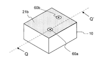
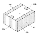
- FIG. 1 is an external perspective view schematically showing a bandpass filter of a first example of an embodiment of the present invention.
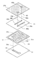
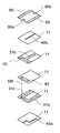
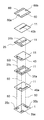
- FIG. 2 is a schematic exploded perspective view of the bandpass filter shown in FIG.
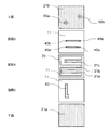
- FIG. 3 is a plan view schematically showing the upper and lower surfaces and layers of the bandpass filter shown in FIG. 4 is a cross-sectional view taken along the line QQ ′ of the bandpass filter shown in FIG.
- the band-pass filter of this example includes a laminate 10, ground electrodes 21a and 21b, first to third resonance electrodes 31a, 31b, and 31c, and a first input / output.
- a coupling electrode 40a, a second input / output coupling electrode 40b, and a resonator coupling electrode 43 are provided.
- the laminate 10 is formed by laminating a plurality of dielectric layers 11.
- the ground electrode 21 a is disposed on the entire lower surface of the multilayer body 10.
- the ground electrode 21b is disposed on almost the entire top surface of the laminate 10.
- the first to third resonance electrodes 31a, 31b, 31c are sequentially arranged side by side as viewed from the stacking direction so as to be electromagnetically coupled to each other between the layers A of the stacked body 10.
- the first to third resonance electrodes 31a, 31b, and 31c are respectively grounded at one end to constitute first to third resonators.
- the first input / output coupling electrode 40a has a strip shape and is disposed in an interlayer B positioned above the interlayer A of the multilayer body 10 so as to be electromagnetically coupled to face the first resonance electrode 31a.
- the second input / output coupling electrode 40b has a strip shape and is disposed in the layer B of the multilayer body 10 so as to be electromagnetically coupled to the second resonance electrode 31b.
- the resonator coupling electrode 43 is disposed in an interlayer C located below the interlayer A of the multilayer body 10, and electromagnetically couples the first resonance electrode 31a and the third resonance electrode 31c.
- a first input / output terminal electrode 60a is disposed on the upper surface of the multilayer body 10 with a gap from the ground electrode 21b, and is connected to the first input / output coupling electrode 40a through the through conductor 50a.
- a second input / output terminal electrode 60b is disposed on the upper surface of the laminate 10 with a space from the ground electrode 21b, and is connected to the second input / output coupling electrode 40b through the through conductor 50b. .
- An annular ground electrode 23 is disposed between the first and third resonance electrodes 31a, 31b, and 31c in the interlayer A of the multilayer body 10.
- the first to third resonance electrodes 31a, 31b, 31c are each connected to the annular ground electrode 23 at one end, and arranged so that the respective one ends are staggered.
- the resonator coupling electrode 43 has one end connected to the other end of the third resonance electrode 31c through the through conductor 50c, and the third resonance electrode 31c and the second end. 3 resonators are configured. Further, the other end of the resonator coupling electrode 43 is opposed to the other end of the first resonance electrode 31a through the dielectric layer 11, and the first resonance electrode 31a is mainly capacitively coupled to the electromagnetic field. is doing.
- the resonance frequencies of the first and second resonators are set to be equal to each other and higher than the resonance frequency of the third resonator.
- the first input / output point 45a at which an electric signal is input to or output from the first input / output coupling electrode 40a is the first resonance at the first input / output coupling electrode 40a. It is closer to the other end of the first resonance electrode 31a than the center of the portion facing the electrode 31a.
- the second input / output point 45b where an electric signal is input to or output from the second input / output coupling electrode 40b is from the center of the second input / output coupling electrode 40b facing the second resonant electrode 31b. Is also on the side close to the other end of the second resonance electrode 31b.
- the first input / output point 45a of the first input / output coupling electrode 40a is externally connected to the first input / output terminal electrode 60a and the through conductor 50a.
- the first resonance electrode 31a electromagnetically coupled to the first input / output coupling electrode 40a is excited and the second resonance electrode 31b electromagnetically coupled to the first input / output coupling electrode 40a resonates.
- the third resonance electrode 31c electromagnetically coupled to the first resonance electrode 31a via the resonator coupling electrode 43 also resonates, and the energy thereof is the third resonance electrode 31c. Is transmitted to the second resonance electrode 31b which is electromagnetically coupled.
- the first and second resonators having the same resonance frequency adjacent to each other are electromagnetically coupled, so that two resonance peaks of even mode and odd mode are generated.
- the third resonator having a resonance frequency lower than that of the first and second resonators is directly electromagnetically coupled to the second resonator and is connected to the first resonance via the resonator coupling electrode 43. And a third resonance peak is generated. Since these three resonance peaks can be used to form a passband, a wideband bandpass filter can be obtained. Further, since the frequencies of the three resonance peaks can be set arbitrarily, a bandpass filter with a high degree of freedom in the design of the passband can be obtained.
- the grounded sides of the first to third resonance electrodes 31a, 31b, 31c are arranged alternately and electromagnetically coupled to the interdigital type. Both the electromagnetic coupling between the first resonance electrode 31a and the second resonance electrode 31b and the electromagnetic coupling between the second resonance electrode 31b and the third resonance electrode 31c are mainly capacitive electromagnetic coupling. .
- the first resonance electrode 31a and the third resonance electrode 31c are mainly capacitively electromagnetically coupled via the resonator coupling electrode 43. As a result, all electromagnetic coupling between the first to third resonators is mainly capacitive electromagnetic coupling.
- the resonance frequency of the first and second resonators is set higher than the resonance frequency of the third resonator, it is directly transmitted from the first resonator to the second resonator.
- phase inversion occurs at a frequency lower than the peak, there is no attenuation pole in the pass band including the three resonance peaks, and an excellent attenuation pole exists outside the pass band on the lower frequency side than the three resonance peaks.
- a bandpass filter having excellent pass characteristics can be obtained.
- the mechanism for obtaining such an effect will be described in more detail. That is, in the band-pass filter of this example, an electrical signal directly transmitted from the first resonance electrode 31a constituting the first resonator to the second resonance electrode 31b constituting the second resonator, There is a signal transmitted from one resonance electrode 31a to the second resonance electrode 31b via the third resonance electrode 31c constituting the third resonator.
- the transmission route of the electric signal directly transmitted from the first resonance electrode 31a to the second resonance electrode 31b is an even mode resonance and an odd mode of the resonance system including the first resonator and the second resonator.
- the first resonance electrode 31a and the second resonance electrode 31b are mainly inductively coupled in the frequency region located outside the two resonance peaks of resonance, the first resonance electrode 31a is equivalent to the inductor.
- the resonant electrode 31a and the second resonant electrode 31b are mainly capacitively coupled, this is equivalent to a capacitor.
- the transmission route of the electric signal transmitted from the first resonance electrode 31a to the second resonance electrode 31b via the third resonance electrode 31c is between the first resonance electrode 31a and the third resonance electrode 31c.
- the resonance frequency of the second resonator When the electromagnetic field coupling and the electromagnetic coupling between the third resonance electrode 31c and the second resonance electrode 31b are both mainly inductive or both mainly capacitive, the resonance frequency of the second resonator. It becomes equivalent to an inductor on the lower frequency side than the capacitor, and equivalent to a capacitor on the higher frequency side than the resonance frequency of the second resonator.
- the transmission route of the electric signal transmitted from the first resonance electrode 31a to the second resonance electrode 31b via the third resonance electrode 31c is between the first resonance electrode 31a and the third resonance electrode 31c.
- the electromagnetic field coupling and the electromagnetic field coupling between the third resonance electrode 31c and the second resonance electrode 31b are mainly inductive electromagnetic field coupling and the other is mainly capacitive electromagnetic field coupling. Is equivalent to a capacitor on the lower frequency side than the resonance frequency of the second resonator, and equivalent to an inductor on the higher frequency side than the resonance frequency of the second resonator.
- the mutual electromagnetic coupling of the first to third resonators is mainly capacitive electromagnetic coupling, and the resonance frequency of the first and second resonators is higher than the resonance frequency of the third resonator. Since it is set high, it is transmitted from the first resonator directly to the second resonator and from the first resonator to the second resonator via the third resonator. Between the signal and the frequency between the three resonance peaks, phase inversion does not occur, and phase inversion occurs at a frequency lower than the three resonance peaks. Therefore, in the pass band including the three resonance peaks, A bandpass filter having no attenuation pole and having excellent pass characteristics having an attenuation pole outside the passband on the lower frequency side than the three resonance peaks can be obtained.
- a resin such as an epoxy resin or a ceramic such as a dielectric ceramic
- a dielectric ceramic material such as BaTiO 3 , Pb 4 Fe 2 Nb 2 O 12 , TiO 2
- a glass material such as B 2 O 3 , SiO 2 , Al 2 O 3 , ZnO, and the like, 800 to 1200 ° C. Glass-ceramic materials that can be fired at relatively low temperatures are preferably used.
- the thickness of the dielectric layer 11 is set to about 0.01 to 0.1 mm, for example.
- Examples of the materials for the various electrodes and through conductors described above include, for example, conductive materials mainly composed of Ag alloys such as Ag, Ag-Pd, and Ag-Pt, Cu-based, W-based, Mo-based, and Pd-based conductive materials. Are preferably used.
- the thicknesses of the various electrodes are set to 0.001 to 0.2 mm, for example.
- the band-pass filter of this example can be manufactured as follows, for example. First, an appropriate organic solvent or the like is added to and mixed with the ceramic raw material powder to produce a slurry, and a ceramic green sheet is formed by a doctor blade method. Next, a through hole for forming a through conductor is formed on the obtained ceramic green sheet using a punching machine or the like, and a conductive paste containing a conductor such as Ag, Ag-Pd, Au, Cu is filled and the ceramic The same conductive paste as described above is applied to the surface of the green sheet using a printing method to produce a ceramic green sheet with a conductive paste. Next, these ceramic green sheets with conductor paste are laminated, pressure-bonded using a hot press apparatus, and fired at a peak temperature of about 800 ° C. to 1050 ° C.
- FIG. 5 is an exploded perspective view schematically showing the band-pass filter of the second example of the embodiment of the present invention.
- FIG. 6 is a plan view schematically showing the upper and lower surfaces and layers of the bandpass filter shown in FIG. Note that in this example, only differences from the first example described above will be described, and the same components will be denoted by the same reference numerals, and redundant description will be omitted.
- the first input / output coupling electrode 40a is arranged in the interlayer C of the multilayer body like the resonator coupling electrode 43.
- the first input / output coupling electrode 40a is connected to the first connection electrode 46 disposed in the interlayer D located below the interlayer C through the through conductor 50d.
- the first connection electrode 46 is connected to the first input / output terminal electrode 60a through the through conductor 50e.
- the first input / output coupling electrode 40a and the second input / output coupling electrode 40b are disposed on the opposite sides of the interlayer A. B and the interlayer C are arranged apart from each other. Thereby, it is possible to prevent the electromagnetic coupling between the first input / output coupling electrode 40a and the second input / output coupling electrode 40b from becoming too strong.
- FIG. 7 is an exploded perspective view schematically showing a band-pass filter of a third example of the embodiment of the present invention.
- FIG. 8 is a plan view schematically showing the upper and lower surfaces and layers of the bandpass filter shown in FIG.
- FIG. 7 only points different from the second example described above will be described, and the same components will be denoted by the same reference numerals, and redundant description will be omitted.
- the band-pass filter of this example is replaced with an annular ground electrode 23, and an inner layer ground electrode 23a to which one end of a first resonance electrode 31a and a third resonance electrode 31c is connected. And an inner layer ground electrode 23b to which one end of the second resonance electrode 31b is connected are arranged between the first layers.
- the first input / output coupling electrode 40a is disposed between the layers B, and the second input / output coupling electrode 40b is disposed between the layers C.
- the third capacitor electrode 35c is disposed in the interlayer D so as to face the ground electrode 21a via the dielectric layer 11, and is connected to the other end of the third resonance electrode 31c via the through conductor 50f. Has been.
- the first input / output coupling electrode 40a and the resonator coupling electrode 43 are disposed between the layers B.
- One end of the resonator coupling electrode 43 is connected to the other end of the first resonance electrode 31a via the through conductor 50g, and the other end of the resonator coupling electrode 43 is connected to the third resonance via the dielectric layer 11. It is electromagnetically coupled to face the other end of the electrode 31c.
- the first connection electrode 46 is disposed in the interlayer E located above the interlayer B.
- the second capacitor electrode 35b is disposed in the interlayer F located above the interlayer E so as to face the ground electrode 21b via the dielectric layer 11, and the second resonance electrode 35b is connected to the second resonance electrode via the through conductor 50h. It is connected to the other end of the electrode 31b.
- the first resonator is constituted by the first resonance electrode 31a, the resonator coupling electrode 43, and the through conductor 50g connecting them, and the second resonance electrode 31b
- the second resonator is constituted by the capacitive electrode 35b and the through conductor 50h connecting the two
- the third resonance is formed by the third resonant electrode 31c, the third capacitive electrode 35c and the through conductor 50f connecting the two.
- the vessel is configured.
- the length of the second resonance electrode 31b can be shortened by the capacitance generated between the second capacitance electrode 35b and the ground electrode 21b. it can. Further, the length of the third resonance electrode 31c can be shortened by the electrostatic capacitance generated between the third capacitance electrode 35c and the ground electrode 21a. Further, the length of the first resonance electrode 31a can be shortened by the resonator coupling electrode 43. Thereby, a small bandpass filter can be obtained.
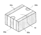
- FIG. 9 is an external perspective view schematically showing the band-pass filter of the fourth example of the embodiment of the present invention.
- FIG. 10 is a schematic exploded perspective view of the bandpass filter shown in FIG.
- FIG. 11 is a plan view schematically showing upper and lower surfaces and layers of the bandpass filter shown in FIG.
- FIG. 10 is a schematic exploded perspective view of the bandpass filter shown in FIG.
- FIG. 11 is a plan view schematically showing upper and lower surfaces and layers of the bandpass filter shown in FIG.
- a dielectric layer 11 is further disposed on the ground electrode 21b disposed on the upper surface of the multilayer body, and is disposed on the lower surface of the multilayer body.
- a dielectric layer 11 is further disposed under the ground electrode 21a, and a new laminate 10 is formed as a whole.
- the first input / output terminal electrode 60 a and the second input / output terminal electrode 60 b are separately arranged on two opposing side surfaces of the multilayer body 10.
- the inner-layer ground electrodes 23a and 23b and the ground terminal electrode 60c connected to the ground electrode 21 are disposed on the two opposite side surfaces of the laminate 10.
- the second input / output coupling electrode 40b is disposed between the layers B, and one end thereof is connected to the second input / output terminal electrode 60b on the side surface of the multilayer body 10. ing. Therefore, the second input / output point 45b is a connection point between the second input / output coupling electrode 40b and the second input / output terminal electrode 60b.
- the first input / output coupling electrode 40a, the resonator coupling electrode 43, and the third connection electrode 36b are arranged in the interlayer C.
- the first connection electrode 46 is disposed between the layers D, one end of which is connected to the first input / output point 45a of the first input / output coupling electrode 40a through the through conductor 50d, and The other end is directly connected to the first input / output terminal electrode 60a on the side surface of the laminate 10.
- the inner layer ground electrode 22c connected to the ground terminal electrode 60c is disposed in the layer E so as to face the third capacitor electrode 35c disposed in the layer F.
- the third capacitor electrode 35c is opposed to the ground electrode 21b disposed in the interlayer G located above the interlayer F via the dielectric layer 11, and is connected to the third capacitor electrode 35f via the through conductor 50f.
- the other end of the resonance electrode 31c is connected.
- the second connection electrode 36a is disposed in the interlayer H located below the interlayer D.
- the interlayer J positioned below the interlayer H includes an inner layer ground electrode 22a disposed to face the first capacitor electrode 35a disposed in the interlayer K positioned below the interlayer J, and an interlayer An inner layer ground electrode 22b disposed to face the second capacitor electrode 35b disposed at K is disposed.
- the two inner layer ground electrodes 22a and 22b arranged in the interlayer J are both connected to the ground terminal electrode 60c.
- the first capacitance electrode 35a is opposed to the ground electrode 21a disposed in the interlayer L located below the interlayer K via the dielectric layer 11, and the second connection electrode 36a via the through conductor 50k. It is connected to the.
- the second connection electrode 36a is connected to the resonator coupling electrode 43 through a through conductor 50m.
- the resonator coupling electrode 43 opposes the other end of the third resonance electrode 31c via the dielectric layer 11, and is connected to the other end of the first resonance electrode 31a via a through conductor 50g.
- the second capacitor electrode 35b faces the ground electrode 21 disposed between the layers L via the dielectric layer 11, and is connected to the third connection electrode 36b via the through conductor 50n.
- the third connection electrode 36b is connected to the other end of the second resonance electrode 31b through the through conductor 50p.
- the first resonance electrode 31a, the resonator coupling electrode 43, the second connection electrode 36a, the first capacitance electrode 35a, and the through conductors 50g, 50m, and 50k that connect them are provided.
- a first resonator is configured.
- the second resonator is constituted by the second resonance electrode 31b, the second connection electrode 36b, the second capacitance electrode 35b, and the through conductors 50p and 50n connecting them.
- a third resonator is constituted by the third resonance electrode 31c, the third capacitance electrode 35c, and the through conductor 50f connecting them.
- the first to third capacitor electrodes 35a, 35b, 35c, the ground electrodes 21a, 21b and the inner-layer ground electrodes 22a, 22b, 22c facing each other are added to the first to third resonators, respectively, so that the lengths of the first to third resonance electrodes 31a, 31b, and 31c can be further shortened. Thereby, a further compact bandpass filter can be obtained.
- FIG. 12 shows an equivalent circuit of the bandpass filters of the third and fourth examples of the embodiment.
- Reference numerals 01 and 02 denote input / output terminals
- 30a, 30b, and 30c denote a first resonator, a second resonator, and a third resonator, respectively.
- the three resonators are all capacitively coupled by capacitors C12, C13, and C23 that are directly coupled between the first to third resonant electrodes 31a, 31b, and 31c or electromagnetically coupled via the resonator coupling electrode 43. .
- a capacitor C60 is formed by electromagnetic coupling between the first input / output coupling electrode 40a and the second input / output coupling electrode 40b, and the first input / output coupling electrode 40a and the second input / output coupling electrode 40b are connected to each other.
- Capacitors C40 and C50 are formed by electromagnetic coupling with the third resonance electrode 31c. With such a configuration, three attenuation poles can be formed on the lower frequency side of the pass band in the pass characteristics of the band pass filter.
- C35, C36, and C37 are the first resonance electrode 31a, the second resonance electrode 31b, and the third resonance electrode formed by the first capacitance electrode 35a, the second capacitance electrode 35b, and the third capacitance electrode 35c.
- FIG. 13 is an external perspective view schematically showing the band-pass filter of the fifth example of the embodiment of the present invention.
- FIG. 14 is a schematic exploded perspective view of the bandpass filter shown in FIG.
- FIG. 15 is a plan view schematically showing the upper and lower surfaces and layers of the bandpass filter shown in FIG.
- the band-pass filter of this example includes a laminate 10, a first input / output terminal electrode 60a, a second input / output terminal electrode 60b, a ground terminal electrode 60c, and a ground. Electrode 21a, internal ground electrode 25, first to third resonance electrodes 31a, 31b, 31c, resonator coupling electrode 43, strip-shaped first input / output coupling electrode 40a, and second input / output coupling And an electrode 40b.
- the laminate 10 is formed by laminating a plurality of dielectric layers 11.
- the ground terminal electrode 60c is disposed over the entire surface of a pair of opposing side surfaces of the multilayer body 10, and is connected to the ground potential.
- the first input / output terminal electrode 60a and the second input / output terminal electrode 60b are disposed on the other pair of opposing side surfaces of the laminate 10 with a gap from the ground terminal electrode 60c.
- the first input / output terminal electrode 60a, the second input / output terminal electrode 60b, and the ground terminal electrode 60c are formed so as to slightly wrap around the upper and lower surfaces of the laminate 10.
- the ground electrode 21a is disposed over substantially the entire bottom surface of the laminate 10, and is connected to the ground terminal electrode 60c.
- the first and third resonance electrodes 31 a and 31 c have a band shape and are arranged side by side with a space between the first layers of the multilayer body 10. One ends of the first and third resonance electrodes 31a and 31c are connected to the ground terminal electrode 60c, respectively, and are grounded to form the first and third resonators.
- the second resonance electrode 31b has a band shape, and is electromagnetically coupled to the first and third resonance electrodes 31a and 31c in the second layer located above the first layer of the multilayer body 10.
- the first and third resonance electrodes 31a and 31c are disposed so as to be seen from the stacking direction (above).
- the first to third resonance electrodes 31a, 31b, 31c are sequentially arranged side by side as viewed from the stacking direction so as to be electromagnetically coupled to each other.
- One end of the second resonance electrode 31b is connected to the ground terminal electrode 60c via an internal ground electrode 25 which is also disposed between the second layers of the laminate 10, and is grounded to connect the second resonator.
- the resonator coupling electrode 43 has a band shape and is disposed between the third and second layers of the multilayer body 10.
- the resonator coupling electrode 43 has one end connected to the other end of the third resonance electrode 31c via the through conductor 50t, and the other end connected to the first resonance electrode via the dielectric layer 11.
- the first and third resonance electrodes 31a and 31c are electromagnetically coupled to each other so as to be opposed to the other end of 31a and to be electromagnetically coupled.
- the first resonance electrode 31a and the third resonance electrode 31c are mainly capacitively electromagnetically coupled via the resonator coupling electrode 43.
- the first input / output coupling electrode 40a has a strip shape and faces the first resonance electrode 31a via the dielectric layer 11 between the fourth layer located below the first layer of the multilayer body 10. Are arranged to be electromagnetically coupled.
- One end of the first input / output coupling electrode 40a is connected to the first input / output terminal electrode 60a.
- the second input / output coupling electrode 40b has a strip shape and faces the second resonance electrode 31b via the dielectric layer 11 between the fifth layer located above the second layer of the multilayer body 10. Are arranged to be electromagnetically coupled. One end of the second input / output coupling electrode 40b is connected to the second input / output terminal electrode 60b.
- the third resonator is constituted by the third resonance electrode 31c, the resonator coupling electrode 43, and the through conductor 50t that connects the third resonance electrode 31c, the resonator coupling electrode 43, and the second resonance electrode 31b and
- the internal ground electrode 25 constitutes a second resonator
- the first resonance electrode 31a constitutes the first resonator.
- the resonance frequencies of the first and second resonators are equal to each other and higher than the resonance frequency of the third resonator, and the passband is configured using the first to third resonators. Is set.
- the passband can be formed using three resonance peaks. Therefore, the bandpass filters of the first to fourth examples of the embodiment described above Similarly, it is possible to obtain a bandpass filter having a wide bandwidth and a high degree of freedom in design of the passband.
- the grounded sides of the first to third resonance electrodes 31a, 31b, 31c are arranged alternately and electromagnetically coupled to the interdigital type, Since the first resonance electrode 31a and the third resonance electrode 31c are mainly capacitively coupled via the resonator coupling electrode 43, all coupling between the first to third resonators is mainly capacitive. It is a bond of sex.
- the resonance frequency of the first and second resonators is set higher than the resonance frequency of the third resonator.
- phase inversion does not occur at frequencies between the three resonance peaks, and phase inversion occurs at frequencies lower than the three resonance peaks. Therefore, there is no attenuation pole in the pass band including the three resonance peaks, and a bandpass filter having excellent pass characteristics having an attenuation pole on the lower frequency side than the pass band can be obtained.
- the ground electrode 21a is disposed on the lower surface of the multilayer body 10, and the first to third resonance electrodes 31a and 31b as viewed from the stacking direction (top) of the multilayer body 10 are provided.
- 31c are arranged on the two side surfaces located at both ends in the direction in which they are arranged side by side and a part of the upper and lower surfaces adjacent to each other. Further, between the first and third resonance electrodes 31a and 31c when viewed from above, between the second layers located above the first layer where the first and third resonance electrodes 31a and 31c are arranged.
- the second resonance electrode 31b is disposed so as to be located at the position.
- the bandpass filter of the present example having such a configuration, the ground electrode 21a, the ground terminal electrode 60c, and the first to third resonance electrodes 31a, 31b, 31c in the laminated body 10 of a limited size. Since the Q value of the first to third resonators can be maximized, a small and low-loss bandpass filter can be obtained.
- FIG. 16 is an exploded perspective view schematically showing a bandpass filter of a sixth example of the embodiment of the present invention.
- FIG. 17 is a plan view schematically showing the upper and lower surfaces and layers of the bandpass filter shown in FIG.
- FIG. 16 only points different from the fifth example described above will be described, and the same components will be denoted by the same reference numerals, and redundant description will be omitted.
- the band-pass filter of this example is disposed so as to face the ground electrode 21a between the fourth interlayer of the multilayer body 10 and the sixth interlayer located below.
- a first capacitor electrode 35a, a second capacitor electrode 35b, and a third capacitor electrode 35c are provided.
- the first capacitor electrode 35a is connected to the other end side of the first resonance electrode 31a through the through conductor 50u.
- the second capacitor electrode 35b is connected to the other end side of the second resonance electrode 31b through the through conductor 50w.
- the third capacitor electrode 35c is connected to the other end side of the third resonance electrode 31c through the through conductor 50x.
- the bandpass filter of this example having such a configuration, capacitance is generated between the first capacitor electrode 35a, the second capacitor electrode 35b, the third capacitor electrode 35c, and the ground electrode 21a.
- the lengths of the first resonance electrode 31a, the third resonance electrode 31c, and the second resonance electrode 31 can be set short. Thereby, a small bandpass filter can be obtained.
- the first resonator is constituted by the first resonance electrode 31a, the first capacitance electrode 35a, and the through conductor 50u connecting both.
- the second resonance electrode 31b, the third capacitance electrode 35c, the through conductor 50 connecting the both, and the internal ground electrode 25 constitute a second resonator.
- the third resonator is constituted by the third resonance electrode 31c, the third capacitance electrode 35c, the resonator coupling electrode 43, and the through conductors 50t and 50x connecting them.
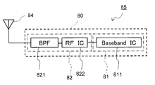
- FIG. 18 is a block diagram showing a wireless communication module 80 and a wireless communication device 85 of the seventh example of the embodiment of the present invention.
- the wireless communication module 80 of this example includes, for example, a baseband unit 81 that processes baseband signals, and an RF unit that is connected to the baseband unit 81 and processes RF signals after modulation and before demodulation of the baseband signals 82.
- the RF unit 82 includes the bandpass filter 821 described above, and an RF signal obtained by modulating the baseband signal or a signal other than the communication band in the received RF signal is attenuated by the bandpass filter 821.
- a baseband IC 811 is arranged in the baseband unit 81, and an RF IC 822 is arranged between the bandpass filter 821 and the baseband unit 81 in the RF unit 82. Note that another circuit may be interposed between these circuits. Then, by connecting the antenna 84 to the band-pass filter 821 of the wireless communication module 80, the wireless communication device 85 of this example that transmits and receives RF signals is configured.
- the bandpass filter 821 of the present invention that can be broadened and has an attenuation pole outside the passband is used for filtering communication signals.
- the loss of communication signals can be reduced over the entire communication band, and noise can be reduced. Therefore, the reception sensitivity is improved and the amplification degree of the communication signal can be reduced, so that the power consumption in the amplifier circuit is reduced. Therefore, a high-performance wireless communication module 80 and wireless communication device 85 with high reception sensitivity and low power consumption can be obtained.
- the grounded sides of the first to third resonance electrodes 31a, 31b, and 31c are arranged alternately so that adjacent resonance electrodes Is mainly capacitive electromagnetic coupling, and the first resonance electrode 31a and the third resonance electrode 31c are mainly capacitive electromagnetic coupling via the resonator coupling electrode 43, and the first and An example in which the resonance frequency of the second resonator is set higher than the resonance frequency of the third resonator is shown.
- the present invention is not limited to this.
- the first to third resonance electrodes 31a, 31b, and 31c are arranged so that the grounded sides are staggered, and the adjacent resonance electrodes are mainly capacitively electromagnetically coupled to each other.
- the electrode 31a and the third resonance electrode 31c are mainly inductively electromagnetically coupled via the resonator coupling electrode 43, and the resonance frequency of the first and second resonators is the resonance of the third resonator. It may be set lower than the frequency.
- phase inversion does not occur at the frequency between the three resonance peaks, and phase inversion occurs at a frequency higher than the three resonance peaks, so there is no attenuation pole in the passband including the three resonance peaks.
- a bandpass filter having an excellent pass characteristic having an attenuation pole on the higher frequency side than the passband.
- both ends of the resonator coupling electrode 43 are connected to each other. While being grounded, one end side of the resonator coupling electrode 43 and one end side of the first resonance electrode 31a face each other and are electromagnetically coupled, and the other end side of the resonator coupling electrode 43 and the third resonance electrode The one end side of 31c may be opposed to be electromagnetically coupled.
- bandpass filter is configured in one laminated body 10
- a band pass filter may be configured across the two.
- the first to third resonance electrodes 31a, 31b, 31c are arranged in the same layer A of the laminate 10 are shown.
- the first and third resonance electrodes 31a and 31c are disposed between the first layers of the laminate 10, and the second resonance electrode 31b is disposed between the first layers.
- positioned between the 2nd layers located on the upper side from this was shown.
- the present invention is not limited to these, and the first to third resonance electrodes 31a, 31b, 31c are arranged side by side as viewed from the stacking direction so as to be electromagnetically coupled to each other between the same or different layers of the stack. As long as they are arranged sequentially.
- the first and second resonance electrodes 31a and 31b may be disposed between the same layers of the multilayer body 10, and the third resonance electrode 31c may be disposed between different layers. Further, the first to third resonance electrodes 31a, 31b, 31c may be arranged between different layers.
- the electrical characteristics of the bandpass filter of the sixth example of the embodiment of the present invention were calculated by simulation using a finite element method.
- the first to third resonance electrodes 31a, 31b, and 31c are rectangular shapes each having a width of 0.25 mm and a length of 1.5 mm.
- the second capacitor electrode 35b was in a square shape with a side of 0.3 mm
- the third capacitor electrode 35c was in a rectangular shape with a width of 0.4 mm and a length of 0.5 mm.
- the resonator coupling electrode 43 has a rectangular shape with a width of 0.1 mm and a length of 1.4 mm.
- the entire bandpass filter was a rectangular parallelepiped having a width of 2.0 mm, a length of 3.0 mm, and a height of 1.0 mm, and the relative dielectric constant of the dielectric layer 11 was 18.7.
- the first resonance electrode 31a has a rectangular shape with a width of 0.35 mm and a length of 1.9 mm.
- the second resonance electrode 31b has a rectangular shape with a width of 0.35 mm and a length of 2.1 mm.
- the third resonance electrode 31c has a rectangular shape with a width of 0.35 mm and a length of 2.2 mm.
- the first capacitor electrode 35a was rectangular with a width of 0.3 mm and a length of 0.88 mm.
- the second capacitor electrode 35b was rectangular with a width of 0.33 mm and a length of 1.1 mm.
- the third capacitor electrode 35c was square with a side of 0.69 mm.
- the first input / output coupling electrode 40a has a rectangular shape with a width of 0.3 mm and a length of 1.4 mm.
- the second input / output coupling electrode 40b has a rectangular shape with a width of 0.14 mm and a length of 2.1 mm.
- the entire bandpass filter was a rectangular parallelepiped having a width of 2.0 mm, a length of 2.5 mm, and a height of 0.9 mm, and the relative dielectric constant of the dielectric layer 11 was 18.7.
- the first resonance electrode 31a has a band shape having a bent portion having a width of 0.31 mm and a length of about 2.4 mm.
- the third resonance electrode 31c was formed in a band shape having a bent portion having a width of 0.31 mm and a length of about 2 mm.
- the second resonance electrode 31b was formed in a strip shape having a width of 0.21 mm and a length of 2 mm.
- the resonator coupling electrode 43 was formed in a strip shape having a width of 0.25 mm and a length of 1.28 mm.
- the first input / output coupling electrode 40a was in the form of a band having a bent portion having a width of 0.15 mm and a length of about 2 mm.
- the second input / output coupling electrode 40b was formed in a strip shape having a width of 0.15 mm and a length of 2 mm.
- the first capacitor electrode 35a was rectangular with a width of 0.6 mm and a length of 0.8 mm.
- the second capacitor electrode 35b was rectangular with a width of 0.6 mm and a length of 1.05 mm.
- the third capacitor electrode 35c was rectangular with a width of 0.35 mm and a length of 1 mm.
- the laminate 10 was a rectangular parallelepiped having a width of 1.6 mm, a length of 2.5 mm, and a thickness of 0.9 mm.
- the relative dielectric constant of the dielectric layer 11 was 18.7.
- FIG. 19 shows the characteristics of the bandpass filter of the third example of the embodiment
- FIG. 20 shows the characteristics of the bandpass filter of the fourth example of the embodiment
- FIG. 21 shows the characteristics of the sixth example of the embodiment. The characteristic of an example band pass filter is shown.
- each has a wide and flat pass band, and three attenuation poles are formed on the lower frequency side than the pass band, so that the attenuation amount on the lower frequency side than the pass band. It can be seen that excellent pass characteristics with sufficiently secured are obtained.
- the attenuation pole located at the frequency closest to the passband is such that the first to third resonators are all capacitively coupled, the resonance frequencies of the first and second resonators are equal, and the resonance frequency of the third resonator.
- the two attenuation poles on the low frequency side are attenuation caused by addition of C40, C50, and C60 in the equivalent circuit shown in FIG. Is the pole.
Landscapes
- Physics & Mathematics (AREA)
- Electromagnetism (AREA)
- Control Of Motors That Do Not Use Commutators (AREA)
Abstract
Description
図1は本発明の実施の形態の第1の例のバンドパスフィルタを模式的に示す外観斜視図である。図2は図1に示すバンドパスフィルタの模式的な分解斜視図である。図3は図1に示すバンドパスフィルタの上下面および層間を模式的に示す平面図である。図4は図1に示すバンドパスフィルタのQ-Q’線断面図である。
図5は本発明の実施の形態の第2の例のバンドパスフィルタを模式的に示す分解斜視図である。図6は図5に示すバンドパスフィルタの上下面および層間を模式的に示す平面図である。なお、本例においては前述した第1の例と異なる点のみについて説明し、同様の構成要素については同一の参照符号を用いて重複する説明を省略する。
図7は本発明の実施の形態の第3の例のバンドパスフィルタを模式的に示す分解斜視図である。図8は図7に示すバンドパスフィルタの上下面および層間を模式的に示す平面図である。なお、本例においては前述した第2の例と異なる点のみについて説明し、同様の構成要素については同一の参照符号を用いて重複する説明を省略する。
図9は本発明の実施の形態の第4の例のバンドパスフィルタを模式的に示す外観斜視図である。図10は図9に示すバンドパスフィルタの模式的な分解斜視図である。図11は図9に示すバンドパスフィルタの上下面および層間を模式的に示す平面図である。なお、本例においては前述した第3の例と異なる点のみについて説明し、同様の構成要素については同一の参照符号を用いて重複する説明を省略する。
(実施の形態の第5の例)
図13は、本発明の実施の形態の第5の例のバンドパスフィルタを模式的に示す外観斜視図である。図14は、図13に示すバンドパスフィルタの模式的な分解斜視図である。図15は、図13に示すバンドパスフィルタの上下面および層間を模式的に示す平面図である。
図16は本発明の実施の形態の第6の例のバンドパスフィルタを模式的に示す分解斜視図である。図17は図16に示すバンドパスフィルタの上下面および層間を模式的に示す平面図である。なお、本例においては前述した第5の例と異なる点のみについて説明し、同様の構成要素については同一の参照符号を用いて重複する説明を省略する。
図18は本発明の実施の形態の第7の例の無線通信モジュール80および無線通信機器85を示すブロック図である。
本発明は前述した実施の形態の第1~第7の例に限定されるものではなく、本発明の要旨を逸脱しない範囲において種々の変更,改良が可能である。
11:誘電体層
21a,21b:接地電極
31a:第1の共振電極
31b:第2の共振電極
31c:第3の共振電極
40a:第1の入出力結合電極
40b:第2の入出力結合電極
43:共振器結合電極
80:無線通信モジュール
81:ベースバンド部
82:RF部
84:アンテナ
85:無線通信機器
821:バンドパスフィルタ
Claims (7)
- 複数の誘電体層が積層されてなる積層体と、
該積層体の上面および下面の少なくとも一方に配置された接地電極と、
前記積層体の同一または異なる層間に、相互に電磁界結合するように積層方向から見て横並びに順次配置された、それぞれ一方端が接地されて第1乃至第3の共振器を構成する帯状の第1乃至第3の共振電極と、
前記積層体の前記第1の共振電極が配置された層間とは異なる層間に、前記第1の共振電極と対向して電磁界結合するように配置された帯状の第1の入出力結合電極と、
前記積層体の前記第2の共振電極が配置された層間とは異なる層間に、前記第2の共振電極と対向して電磁界結合するように配置された帯状の第2の入出力結合電極と、
前記積層体の前記第1の共振電極が配置された層間および前記第3の共振電極が配置された層間とは異なる層間に配置された、前記第1の共振電極および前記第3の共振電極を電磁界結合する共振器結合電極とを備え、
前記第1および第2の共振器の共振周波数は互いに等しく且つ前記第3の共振器の共振周波数と異なる周波数に設定されており、
前記第1乃至第3の共振器を用いて通過帯域を構成することを特徴とするバンドパスフィルタ。 - 前記第1乃至第3の共振電極は前記積層体の同一の層間に配置されていることを特徴とする請求項1に記載のバンドパスフィルタ。
- 前記接地電極は前記積層体の下面に配置されており、
前記第1および第3の共振電極は前記積層体の第1の層間に間隔を開けて横並びに配置されており、
前記第2の共振電極は、前記積層体の前記第1の層間よりも上側に位置する第2の層間に、積層方向から見て前記第1および第3の共振電極の間に位置するように配置されていることを特徴とする請求項1に記載のバンドパスフィルタ。 - 前記第1乃至第3の共振電極は、積層方向から見てそれぞれの接地される側が互い違いになるように配置されており、前記第1の共振電極と前記第3の共振電極とは、前記共振器結合電極を介して主に容量性の電磁界結合をしており、前記第1および第2の共振器の共振周波数は前記第3の共振器の共振周波数よりも高く設定されていることを特徴とする請求項1乃至請求項3のいずれかに記載のバンドパスフィルタ。
- 前記第1乃至第3の共振電極は、積層方向から見てそれぞれの接地される側が互い違いになるように配置されており、前記第1の共振電極と前記第3の共振電極とは、前記共振器結合電極を介して主に誘導性の電磁界結合をしており、前記第1および第2の共振器の共振周波数は前記第3の共振器の共振周波数よりも低く設定されていることを特徴とする請求項1乃至請求項3のいずれかに記載のバンドパスフィルタ。
- 請求項1乃至請求項5のいずれかに記載のバンドパスフィルタを含むRF部と、該RF部に接続されたベースバンド部とを備えることを特徴とする無線通信モジュール。
- 請求項1乃至請求項5のいずれかに記載のバンドパスフィルタを含むRF部と、該RF部に接続されたベースバンド部と、前記RF部に接続されたアンテナとを備えることを特徴とする無線通信機器。
Priority Applications (2)
| Application Number | Priority Date | Filing Date | Title |
|---|---|---|---|
| US13/131,236 US8878634B2 (en) | 2008-11-26 | 2009-11-24 | Bandpass filter, and wireless communication module and wireless communication device using the bandpass filter |
| JP2010540477A JP5300865B2 (ja) | 2008-11-26 | 2009-11-24 | バンドパスフィルタならびにそれを用いた無線通信モジュールおよび無線通信機器 |
Applications Claiming Priority (4)
| Application Number | Priority Date | Filing Date | Title |
|---|---|---|---|
| JP2008300730 | 2008-11-26 | ||
| JP2008-300730 | 2008-11-26 | ||
| JP2009-041983 | 2009-02-25 | ||
| JP2009041983 | 2009-02-25 |
Publications (1)
| Publication Number | Publication Date |
|---|---|
| WO2010061815A1 true WO2010061815A1 (ja) | 2010-06-03 |
Family
ID=42225689
Family Applications (1)
| Application Number | Title | Priority Date | Filing Date |
|---|---|---|---|
| PCT/JP2009/069792 Ceased WO2010061815A1 (ja) | 2008-11-26 | 2009-11-24 | バンドパスフィルタならびにそれを用いた無線通信モジュールおよび無線通信機器 |
Country Status (3)
| Country | Link |
|---|---|
| US (1) | US8878634B2 (ja) |
| JP (1) | JP5300865B2 (ja) |
| WO (1) | WO2010061815A1 (ja) |
Families Citing this family (3)
| Publication number | Priority date | Publication date | Assignee | Title |
|---|---|---|---|---|
| CN103828249B (zh) * | 2011-09-26 | 2016-08-17 | 株式会社村田制作所 | 高频模块 |
| CN103985929B (zh) * | 2014-05-09 | 2016-08-17 | 南京理工大学 | 一种高抑制模块化微型带通滤波器 |
| EP3912222B1 (en) * | 2019-01-15 | 2024-05-01 | Telefonaktiebolaget LM Ericsson (publ) | Miniature filter design for antenna systems |
Citations (5)
| Publication number | Priority date | Publication date | Assignee | Title |
|---|---|---|---|---|
| JPH0870201A (ja) * | 1994-08-26 | 1996-03-12 | Japan Radio Co Ltd | 積層誘電体フィルタ |
| JP2006033614A (ja) * | 2004-07-20 | 2006-02-02 | Tdk Corp | 積層型誘電体フィルタ |
| JP2006166136A (ja) * | 2004-12-08 | 2006-06-22 | Koa Corp | 積層型バンドパスフィルタ |
| JP2008271485A (ja) * | 2006-10-13 | 2008-11-06 | Kyocera Corp | バンドパスフィルタおよびそれを用いた高周波モジュールならびにそれらを用いた無線通信機器 |
| JP2009105865A (ja) * | 2007-10-01 | 2009-05-14 | Kyocera Corp | フィルタ装置 |
Family Cites Families (11)
| Publication number | Priority date | Publication date | Assignee | Title |
|---|---|---|---|---|
| JPH067973A (ja) * | 1992-06-25 | 1994-01-18 | Fanuc Ltd | レーザ加工装置 |
| KR0148749B1 (ko) | 1992-10-14 | 1998-08-17 | 모리시다 요오이찌 | 필터 및 그 제조방법 |
| JP3173230B2 (ja) | 1993-07-12 | 2001-06-04 | 松下電器産業株式会社 | フィルタの製造方法 |
| US6294967B1 (en) * | 1998-03-18 | 2001-09-25 | Ngk Insulators, Ltd. | Laminated type dielectric filter |
| TW501308B (en) * | 2001-11-07 | 2002-09-01 | Ind Tech Res Inst | Asymmetric high-frequency filtering structure |
| US7652548B2 (en) * | 2005-04-25 | 2010-01-26 | Kyocera Corporation | Bandpass filter, high-frequency module, and wireless communications equipment |
| KR100972760B1 (ko) | 2006-05-29 | 2010-07-28 | 쿄세라 코포레이션 | 대역 통과 필터 및 그것을 이용한 고주파 모듈 및 그것들을 이용한 무선 통신 기기 |
| US8093963B2 (en) * | 2006-12-01 | 2012-01-10 | Hitachi Metals, Ltd. | Laminated bandpass filter, high-frequency component and communications apparatus comprising them |
| JP5213419B2 (ja) * | 2007-04-18 | 2013-06-19 | 京セラ株式会社 | バンドパスフィルタならびにそれを用いた無線通信モジュールおよび無線通信機器 |
| WO2008132927A1 (ja) * | 2007-04-18 | 2008-11-06 | Kyocera Corporation | バンドパスフィルタならびにそれを用いた無線通信モジュールおよび無線通信機器 |
| JP4610584B2 (ja) * | 2007-06-26 | 2011-01-12 | 京セラ株式会社 | バンドパスフィルタならびにそれを用いた無線通信モジュールおよび無線通信機器 |
-
2009
- 2009-11-24 WO PCT/JP2009/069792 patent/WO2010061815A1/ja not_active Ceased
- 2009-11-24 JP JP2010540477A patent/JP5300865B2/ja not_active Expired - Fee Related
- 2009-11-24 US US13/131,236 patent/US8878634B2/en active Active
Patent Citations (5)
| Publication number | Priority date | Publication date | Assignee | Title |
|---|---|---|---|---|
| JPH0870201A (ja) * | 1994-08-26 | 1996-03-12 | Japan Radio Co Ltd | 積層誘電体フィルタ |
| JP2006033614A (ja) * | 2004-07-20 | 2006-02-02 | Tdk Corp | 積層型誘電体フィルタ |
| JP2006166136A (ja) * | 2004-12-08 | 2006-06-22 | Koa Corp | 積層型バンドパスフィルタ |
| JP2008271485A (ja) * | 2006-10-13 | 2008-11-06 | Kyocera Corp | バンドパスフィルタおよびそれを用いた高周波モジュールならびにそれらを用いた無線通信機器 |
| JP2009105865A (ja) * | 2007-10-01 | 2009-05-14 | Kyocera Corp | フィルタ装置 |
Also Published As
| Publication number | Publication date |
|---|---|
| US8878634B2 (en) | 2014-11-04 |
| JP5300865B2 (ja) | 2013-09-25 |
| JPWO2010061815A1 (ja) | 2012-04-26 |
| US20110237216A1 (en) | 2011-09-29 |
Similar Documents
| Publication | Publication Date | Title |
|---|---|---|
| JP5044654B2 (ja) | バンドパスフィルタならびにそれを用いた無線通信モジュールおよび無線通信機器 | |
| KR100972760B1 (ko) | 대역 통과 필터 및 그것을 이용한 고주파 모듈 및 그것들을 이용한 무선 통신 기기 | |
| JP4818207B2 (ja) | バンドパスフィルタおよびそれを用いた高周波モジュールならびにそれらを用いた無線通信機器 | |
| JP5153246B2 (ja) | バンドパスフィルタならびにそれを用いた無線通信モジュールおよび無線通信機器 | |
| JP4923111B2 (ja) | ダイプレクサならびにそれを用いた無線通信モジュールおよび無線通信機器 | |
| JP5300865B2 (ja) | バンドパスフィルタならびにそれを用いた無線通信モジュールおよび無線通信機器 | |
| JP5305809B2 (ja) | 分波器ならびにそれを用いた無線通信モジュールおよび無線通信機器 | |
| JP4600456B2 (ja) | フィルタ | |
| JP5288903B2 (ja) | バンドパスフィルタならびにそれを用いた無線通信モジュールおよび無線通信機器 | |
| JP4849959B2 (ja) | バンドパスフィルタおよびそれを用いた高周波モジュールならびにそれらを用いた無線通信機器 | |
| US20110006857A1 (en) | Complex resonator, bandpass filter, and diplexer, and wireless communication module and wireless communication device using same | |
| JP4610585B2 (ja) | バンドパスフィルタおよびそれを用いた高周波モジュールならびにそれらを用いた無線通信機器 | |
| JP5288904B2 (ja) | バンドパスフィルタならびにそれを用いた無線通信モジュールおよび無線通信機器 | |
| JP5116653B2 (ja) | バンドパスフィルタならびにそれを用いた無線通信モジュールおよび無線通信機器 | |
| JP4889539B2 (ja) | バンドパスフィルタおよびそれを用いた高周波モジュールならびにそれらを用いた無線通信機器 | |
| JP5171710B2 (ja) | バンドパスフィルタならびにそれを用いた無線通信モジュールおよび無線通信機器 | |
| JP4610584B2 (ja) | バンドパスフィルタならびにそれを用いた無線通信モジュールおよび無線通信機器 | |
| JP2009033525A (ja) | バンドパスフィルタならびにそれを用いた無線通信モジュールおよび無線通信機器 | |
| JP2010232779A (ja) | ダイプレクサならびにそれを用いた無線通信モジュールおよび無線通信機器 | |
| JP5224908B2 (ja) | バンドパスフィルタならびにそれを用いた無線通信モジュールおよび無線通信機器 | |
| JP5288885B2 (ja) | バンドパスフィルタならびにそれを用いた無線通信モジュールおよび無線通信機器 | |
| JP2009206545A (ja) | バンドパスフィルタならびにそれを用いた無線通信モジュールおよび無線通信機器 | |
| WO2009145277A1 (ja) | バンドパスフィルタならびにそれを用いた無線通信モジュールおよび無線通信機器 | |
| JP2009232168A (ja) | ダイプレクサならびにそれを用いた無線通信モジュールおよび無線通信機器 | |
| JP2010199950A (ja) | バンドパスフィルタならびにそれを用いた無線通信モジュールおよび無線通信機器 |
Legal Events
| Date | Code | Title | Description |
|---|---|---|---|
| 121 | Ep: the epo has been informed by wipo that ep was designated in this application |
Ref document number: 09829063 Country of ref document: EP Kind code of ref document: A1 |
|
| ENP | Entry into the national phase |
Ref document number: 2010540477 Country of ref document: JP Kind code of ref document: A |
|
| WWE | Wipo information: entry into national phase |
Ref document number: 13131236 Country of ref document: US |
|
| NENP | Non-entry into the national phase |
Ref country code: DE |
|
| 122 | Ep: pct application non-entry in european phase |
Ref document number: 09829063 Country of ref document: EP Kind code of ref document: A1 |