WO2010058675A1 - マルチバンドアンテナ - Google Patents
マルチバンドアンテナ Download PDFInfo
- Publication number
- WO2010058675A1 WO2010058675A1 PCT/JP2009/068123 JP2009068123W WO2010058675A1 WO 2010058675 A1 WO2010058675 A1 WO 2010058675A1 JP 2009068123 W JP2009068123 W JP 2009068123W WO 2010058675 A1 WO2010058675 A1 WO 2010058675A1
- Authority
- WO
- WIPO (PCT)
- Prior art keywords
- antenna
- substrate
- distributor
- distributors
- elements
- Prior art date
- Legal status (The legal status is an assumption and is not a legal conclusion. Google has not performed a legal analysis and makes no representation as to the accuracy of the status listed.)
- Ceased
Links
Images



Classifications
-
- H—ELECTRICITY
- H01—ELECTRIC ELEMENTS
- H01Q—ANTENNAS, i.e. RADIO AERIALS
- H01Q21/00—Antenna arrays or systems
- H01Q21/06—Arrays of individually energised antenna units similarly polarised and spaced apart
- H01Q21/08—Arrays of individually energised antenna units similarly polarised and spaced apart the units being spaced along or adjacent to a rectilinear path
- H01Q21/10—Collinear arrangements of substantially straight elongated conductive units
-
- H—ELECTRICITY
- H01—ELECTRIC ELEMENTS
- H01Q—ANTENNAS, i.e. RADIO AERIALS
- H01Q1/00—Details of, or arrangements associated with, antennas
- H01Q1/36—Structural form of radiating elements, e.g. cone, spiral, umbrella; Particular materials used therewith
- H01Q1/38—Structural form of radiating elements, e.g. cone, spiral, umbrella; Particular materials used therewith formed by a conductive layer on an insulating support
-
- H—ELECTRICITY
- H01—ELECTRIC ELEMENTS
- H01Q—ANTENNAS, i.e. RADIO AERIALS
- H01Q21/00—Antenna arrays or systems
- H01Q21/30—Combinations of separate antenna units operating in different wavebands and connected to a common feeder system
-
- H—ELECTRICITY
- H01—ELECTRIC ELEMENTS
- H01Q—ANTENNAS, i.e. RADIO AERIALS
- H01Q5/00—Arrangements for simultaneous operation of antennas on two or more different wavebands, e.g. dual-band or multi-band arrangements
-
- H—ELECTRICITY
- H01—ELECTRIC ELEMENTS
- H01Q—ANTENNAS, i.e. RADIO AERIALS
- H01Q5/00—Arrangements for simultaneous operation of antennas on two or more different wavebands, e.g. dual-band or multi-band arrangements
- H01Q5/30—Arrangements for providing operation on different wavebands
- H01Q5/307—Individual or coupled radiating elements, each element being fed in an unspecified way
- H01Q5/342—Individual or coupled radiating elements, each element being fed in an unspecified way for different propagation modes
- H01Q5/357—Individual or coupled radiating elements, each element being fed in an unspecified way for different propagation modes using a single feed point
- H01Q5/364—Creating multiple current paths
- H01Q5/371—Branching current paths
-
- H—ELECTRICITY
- H01—ELECTRIC ELEMENTS
- H01Q—ANTENNAS, i.e. RADIO AERIALS
- H01Q5/00—Arrangements for simultaneous operation of antennas on two or more different wavebands, e.g. dual-band or multi-band arrangements
- H01Q5/40—Imbricated or interleaved structures; Combined or electromagnetically coupled arrangements, e.g. comprising two or more non-connected fed radiating elements
- H01Q5/42—Imbricated or interleaved structures; Combined or electromagnetically coupled arrangements, e.g. comprising two or more non-connected fed radiating elements using two or more imbricated arrays
-
- H—ELECTRICITY
- H01—ELECTRIC ELEMENTS
- H01Q—ANTENNAS, i.e. RADIO AERIALS
- H01Q9/00—Electrically-short antennas having dimensions not more than twice the operating wavelength and consisting of conductive active radiating elements
- H01Q9/04—Resonant antennas
- H01Q9/16—Resonant antennas with feed intermediate between the extremities of the antenna, e.g. centre-fed dipole
- H01Q9/28—Conical, cylindrical, cage, strip, gauze, or like elements having an extended radiating surface; Elements comprising two conical surfaces having collinear axes and adjacent apices and fed by two-conductor transmission lines
Definitions
- the present invention relates to a multiband antenna used as a simple base station antenna in mobile radio communication such as a mobile phone.
- a non-directional antenna for a base station in mobile radio communication such as PHS
- a parallel feeding collinear antenna provided with multiple stages of dipole antenna elements is generally used (for example, see Patent Document 1).
- a conventional parallel-feed collinear antenna is composed of an antenna board provided with multi-stage antenna elements and a distribution board that distributes a feed signal to the antenna element, and the distribution board is connected to the lower side of the antenna board. Yes.
- the conventional parallel-fed collinear antenna requires a distribution board that distributes the feed signal in addition to the antenna board, which increases the number of components and is troublesome to manage, and can only cover the frequency of one wave. There was a problem.
- the present invention has been made to solve the above problems, and by providing a plurality of distributors on the antenna board, it is possible to feed power to each antenna element in parallel without providing an independent distribution board.
- An object of the present invention is to provide a multiband antenna that can be easily managed by reducing the frequency and can share two frequencies.
- One embodiment of the present invention is a first to fourth antenna element having a substrate formed in a strip shape and a plurality of radiating elements that are provided on the front surface of the substrate at predetermined intervals in the longitudinal direction and operate in different frequency bands.
- the first to fourth distributors provided between the lower end of the substrate and each antenna element, and the feed signal provided along the front center of the substrate and distributed by the corresponding distributor.
- a multiband antenna Provided is a multiband antenna.
- power can be supplied to each antenna element without providing an independent distribution board, the number of parts can be reduced, management can be facilitated, and two frequencies can be shared.
- the two distributors between the antenna elements it is possible to avoid disturbance in directivity due to power feeding.
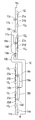
- FIG. 1 is a diagram showing a schematic configuration of a multiband antenna and a feeding system according to an embodiment of the present invention.
- FIG. 2 is a diagram illustrating a wiring state of a feeder line with respect to each antenna substrate in the embodiment.
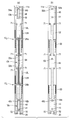
- FIG. 3 shows a configuration example of an antenna element and a distributor provided on the antenna substrate in the same embodiment, where (a) shows a copper foil pattern on the front side, and (b) shows a copper foil pattern on the back side.
- FIG. FIG. 4 is an enlarged view of the main part of the antenna substrate in FIG. 3, wherein (a) is a front side copper foil pattern, and (b) is a back side copper foil pattern.
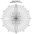
- FIG. 5 is a diagram showing the vertical polarization vertical plane directivity in the same embodiment.
- FIG. 6 is a diagram illustrating the vertical polarization vertical plane directivity when the upper ground pattern and the lower ground pattern are directly connected and no capacitor is provided in the same embodiment.
- FIG. 1 is a diagram showing a schematic configuration of a multiband antenna and a feeding system according to an embodiment of the present invention.
- the multiband antenna according to this embodiment shares two frequencies, for example, a low frequency band f L of 1.9 GHz and a high frequency band f H of 2.56 GHz, and a plurality of antenna boards 11a and 11b, for example, are arranged in series. It is arranged.
- Frequency ratio of the low frequency band f L and the high frequency band f H is about 1: is set to 1.3-1.4.
- the antenna substrates 11a and 11b On the antenna substrates 11a and 11b, a plurality of stages, for example, four stages of antenna elements 12 1 , 12 2 ,... In the example shown in FIG. 1, since two antenna substrates 11a and 11b are used, eight stages of antenna elements 12 1 to 12 8 are arranged in tandem.
- the antenna substrates 11a and 11b are formed of an insulating member (dielectric material) having elasticity, for example.
- Each of the antenna elements 12 1 to 12 8 includes a radiating element (high frequency band element) 12 H whose operating band is the high frequency band f H and a radiating element (low frequency band element) whose operating band is the low frequency band f L. ) 12 L.
- the front and back surfaces of the antenna substrates 11a and 11b are constituted by copper foil patterns.
- the antenna boards 11a and 11b are each provided with four distributors.
- the upper antenna substrate 11 a is provided with the first two distributors 13 a below the antenna elements 124 4 , and between the antenna elements 12 2 and 12 3 , the second two distributors 13 b and the antenna elements 12.
- a third distributor 13 c is provided between 1 and 12 2
- a fourth distributor 13 d is provided between the antenna elements 12 3 and 12 4 .
- the input terminals of the two distributors 13a to 13d are provided on the back side of the antenna substrate 11a.
- the distribution output terminal of the third two-divider 13c is connected to the feeding points 22a and 22b of the antenna elements 12 1 and 12 2 via the feeding strip lines 21a and 21b provided on the antenna substrate 11a.
- Division output terminal of the fourth 2 distributor 13d is feeding strip line 21c provided on the antenna substrate 11a, the antenna element 12 3 through 21d, 12 4 of the feeding point 22c, is connected to 22d.
- the lower of the antenna substrate 11b, with the first 2 distributor 14a is provided on the lower side of the antenna elements 12 8, a second 2 distributor 14b to the antenna elements 12 6, 12 7, antenna element 12 5, 12 between 6 third two distributor 14c, a fourth divider 14d is provided between the antenna element 12 7, 12 8.
- the input terminals of the two distributors 14a to 14d are provided on the back side of the antenna substrate 11b.
- Distribution output terminal of the third 2 distributor 14c is feeding strip line 23a provided on the antenna substrate 11b, the antenna elements 12 5, 12 6 of the feeding point 24a through 23b, are connected to 24b.
- Division output terminal of the fourth 2 distributor 14d is feeding strip line 23c provided on the antenna substrate 11b, the antenna element 12 7, 12 8 feeding points 24c through 23d, is connected to 24d.
- the input terminal of the first two distributors 13a provided on the upper antenna substrate 11a is connected to a transceiver (not shown) by a feeder 15 using a 50 ⁇ semi-flexible coaxial cable, for example.
- the two distributors 13a distribute the power supply signal supplied from the transmitter / receiver by the power supply line 15, and the second distributor 13a is connected to the second antenna substrates 11a and 11b via the power supply lines 16a and 16b which are coaxial cables similar to the power supply line 15.
- the two distributors 13b and 14b are fed.
- the second two distributor 13b of the antenna substrate 11a distributes the feeding signal inputted through the feeding line 16a into two, and the third two distributor 13c and the fourth 2 through the feeding lines 17a and 17b. Input to the distributor 13d.
- the third two-distributor 13c distributes the feeding signal input through the feeding line 17a into two , and feeds the feeding points 22a and 22b of the antenna elements 12 1 and 12 2 through the feeding strip lines 21a and 21b.
- the fourth 2 distributor 13d is a power supply signal inputted via the power supply line 17b 2 distributed, feeding strip line 21c, the antenna element 12 3 through 21d, 12 4 of the feeding point 22c, to 22d Supply power.
- the second two distributors 14b of the lower antenna board 11b distribute the power feeding signal input through the power feeding line 16b into two, and the third two distributors 14c and the second power distributors through the power feeding lines 18a and 18b. 4 to the two dividers 14d.
- Third two distributor 14c is a power supply signal input via the power supply lines 18a 2 and partitioned, feeding strip line 23a, the antenna element 12 via 23b 5, 12 6 of the feeding point 24a, power supply to 24b To do.
- the fourth 2 distributor 14d is a power supply signal inputted via the power supply line 18b 2 distributed, feeding strip line 23c, the antenna element 12 7, 12 8 feeding points 24c through 23d, the 24d Supply power.
- the first two distributors 14a provided on the lower antenna board 11b are: do not use.
- the antenna substrates 11a and 11b are positioned by alternately inverting the front surface (element forming surface) and the back surface (earth surface), and feeding lines 15, 16a, 16b, 17a, 17b, and the center along the back surface side. 18a and 18b are wired.
- the antenna boards 11a and 11b are provided with notches 20 at the upper and lower ends, and the feeder lines 15 and 16b and the like can be inserted into the notches 20.
- FIG. 2 shows a specific wiring state of the feeder lines 15, 16a, 16b, 17a, 17b, 18a, and 18b.
- the antenna substrates 11a and 11b are arranged so that the front surface (element formation surface) and the back surface (earth surface) are alternately reversed.
- the right side of the upper antenna substrate 11a is the front and lower antennas.
- the left side of the substrate 11b is the front surface.
- the feeder 15 connected to the transceiver is wired along the center of the back surface of the lower antenna substrate 11b, passes through the notch 20 between the antenna substrates 11a and 11b, and the upper antenna substrate 11a. Is connected to the input terminal of the first two distributor 13a of the antenna substrate 11a. One of the distribution output terminals of the two distributors 13a is connected to the input terminal of the second two distributors 13b through the feeder line 16a on the back surface of the antenna substrate 11a. The other of the distribution output terminals of the two distributors 13a passes through the notch 20 between the antenna substrates 11a and 11b and is led out to the back side of the lower antenna substrate 11b. It is connected to the input terminal of the distributor 14b.
- the distribution output terminal of the second two distributor 13b in the upper antenna board 11a is connected to the input terminals of the third and fourth two distributors 13c and 13d through the feed lines 17a and 17b on the back surface of the antenna board 11a. Is done.
- the distribution output terminal of the second two distributors 14b in the lower antenna board 11b is connected to the input terminals of the third and fourth two distributors 14c and 14d through the feed lines 18a and 18b on the back surface of the antenna board 11b. .
- Power supply in the unbalanced mode is performed from the power supply line 15 to at least the two distributors 13c, 13d, 14c, and 14d.
- FIG. 3 shows a configuration example of the first to fourth antenna elements 12 1 to 12 4 and the two distributors 13a to 13d provided on the antenna substrate 11a.
- FIG. 3A shows a copper foil pattern on the front side.
- (B) shows the copper foil pattern on the back side. These patterns are basically symmetrical.
- FIG. 4 is an enlarged view of the main part of the antenna substrate 11a in FIG. 3, that is, the third and fourth antenna elements 12 3 and 12 4 and the two distributors 13a, 13b, and 13d. a) shows the copper foil pattern on the front side, and (b) shows the copper foil pattern on the back side.
- the circuit pattern of the antenna elements 12 1 to 12 4 are provided at predetermined intervals, the first 2 distributor below the antenna element 12 4 13a, a second two distributor 13b between the antenna elements 12 2 and 12 3 , a third two distributor 13c between the antenna elements 12 1 and 12 2 , and a fourth distributor between the antenna elements 12 3 and 12 4
- a circuit pattern of 13d is provided.
- Each of the antenna elements 12 1 to 12 4 includes the high frequency band element 12 H and the low frequency band element 12 L as described above, and has a length of about 1/2 wavelength on both sides on the front side of the antenna substrate 11a.
- An element is provided.
- the high frequency band element 12H is disposed outside the front surface of the substrate, and the low frequency band element 12L is disposed inside thereof.
- the high frequency band element 12 H and the low frequency band element 12 L are composed of an upper element and a lower element having a length of about 1 ⁇ 4 wavelength, with the upper element on the “+” side and the lower element on the “ ⁇ ” side. Yes.
- the high frequency band element 12 H and the low frequency band element 12 L are bent inward at the opposing ends of the upper element and the lower element and connected to the feeding point 22.
- the length La of the high frequency band element 12 H and the length Lb of the low frequency band element 12 L are basically set to 1 ⁇ 2 wavelength, but considering the wavelength shortening rate of the antenna substrates 11a and 11b. Is set.
- the length La of the high-frequency band element 12 H is about 0.37 ⁇ H
- the length Lb of the lower frequency band element 12 L is set to about 0.42 ⁇ L.
- the ⁇ H indicates a wavelength in a high frequency band such as 2.56 GHz
- ⁇ L indicates a wavelength in a low frequency band such as 1.9 GHz.
- the antenna substrate 11a (11b) having a dielectric constant of about 3.3 is used, and the wavelength shortening rate at that time is about 0.55.
- the width, length, interval, pattern thickness, etc. of the elements are designed so that the impedance viewed from each feeding point 22 of the antenna elements 12 1 to 12 4 is about 100 ⁇ .
- a ground pattern 31 is formed in an empty area of the antenna elements 12 1 to 12 4 and the two distributors 13a to 13d, that is, so as not to obstruct circuit elements.
- a ground pattern 32 having a predetermined width is formed along the center position on the back surface of the antenna substrate 11a, and the high frequency band element 12H and the low frequency band element 12 constituting each of the antenna elements 12 1 to 12 4 are formed.
- a pattern 33 constituting an L lower element is provided.
- the pattern 33 has substantially the same shape as the pattern of the lower elements of the high frequency band element 12 H and the low frequency band element 12 L provided on the front surface side, and the front surface and the back surface are connected by a plurality of through holes. It has become. Further, the ground pattern 32 on the back side is connected to the ground pattern 31 on the front side by a plurality of through holes.
- the first to fourth two distributors 13a to 13d are provided on the front side of the antenna substrate 11a.
- the two distributors 13a to 13b are basically constituted by a ⁇ M / 4 transformer and a point distributor, but the length is set according to the wavelength shortening rate determined by the dielectric constant of the antenna substrate 11a.
- the ⁇ M indicates a wavelength at an intermediate frequency between the high frequency band and the low frequency band.
- the first 2 distributors 13a provided on the lower side of the antenna element 12 4 is constituted by a line pattern 40.
- the line pattern 40 is a vertical linear microstrip line having a characteristic impedance of ⁇ (50 ⁇ 25) ⁇ 35 ⁇ , and one through hole 41 is provided at the lower end portion and two through holes are provided at the upper end portion. Holes 42a and 42b are provided.
- a distributor ground pattern 43 is formed on the back side of the antenna substrate 11a at a position corresponding to the line pattern 40 of the first two distributors 13a.
- an input terminal 45 is provided at a position corresponding to the through hole 41
- distribution output terminals 46a and 46b are provided at positions corresponding to the through holes 42a and 42b. , 42a, 42b to the line pattern 40 of the two distributor 13a.
- the input terminal 45 and the distribution output terminals 46 a and 46 b are provided in a state of being insulated from the distributor ground pattern 43.
- the input terminal 45 of the first two distributor 13a is connected to the feeder line 15 from the transceiver, and the distribution output terminals 46a and 46b are connected to the input terminal 45a by the feeder lines 16a and 16b.
- the second two distributors 13b and the second two distributors 14b of the lower antenna board 11b are connected.
- the second two-distributor 13b includes a circuit pattern 48 provided on the front surface side of the antenna substrate 11a and a square-shaped distributor earth pattern 49 provided on the back surface side.
- a circuit pattern 48 provided on the front surface side of the antenna substrate 11a and a square-shaped distributor earth pattern 49 provided on the back surface side.
- an input terminal 51 is provided at the center, and distribution output terminals 52a and 52b are provided at the top.
- the input terminal 51 and the distribution output terminals 52 a and 52 b are provided in a state of being insulated from the distributor ground pattern 49.
- the input terminal 51 is connected to the front circuit pattern 48 through a through hole 53, and the distribution output terminals 52a and 52b are connected to the circuit pattern 48 through through holes 54a and 54b. That is, the signal input to the input terminal 51 is divided into two by the circuit pattern 48 and output from the distribution output terminals 52a and 52b.
- the ground pattern is vertically divided into two parts as shown in an enlarged view of section A, and the landscape pattern is horizontally long between the upper ground pattern and the lower ground pattern.
- the capacitor elements 56a are simply formed by arranging the element patterns 55a and 55b facing each other at a minute interval.
- the ground pattern is divided into two vertically below the input terminal 51 provided on the second two distributor 13b, and a horizontally long element pattern is finely formed between the upper ground pattern and the lower ground pattern.
- Capacitor elements 56b are simply formed so as to face each other at intervals.
- the ground pattern provided on the front surface and the back surface of the antenna substrate 11a is divided into two vertically at the center portion, and the capacitor elements 56a and 56b are formed between them, so that the high frequency band element 12H side of the antenna element in particular. Directivity is improved by preventing current leakage in
- the distribution output terminals 52a and 52b of the second two distributor 13b are connected to the input terminals of the third two distributor 13c and the fourth distributor 13d through power supply lines 17a and 17b, respectively.
- a rectangular distributor ground pattern 58 is formed on the back side of the antenna substrate 11 a, and an input terminal 59 is provided in the distributor ground pattern 58. Is provided.
- the input terminal 59 is provided in an insulated state from the distributor ground pattern 58 and led out to the front side of the substrate through the through hole 60.
- the through hole 60 led to the front side of the substrate constitutes a distribution output terminal, and is connected to the feeding points 22a and 22b of the antenna elements 12 1 and 12 2 by the feeding strip lines 21a and 21b.
- the feeding strip lines 21a and 21b are formed along the front center of the antenna substrate 11a.
- the feeding strip lines 21a and 21b are, for example, microstrip lines whose characteristic impedance is set to about 100 ⁇ , and the combined impedance of the through-hole 60 which is the branch output terminal of the third two distributor 13c is about 50 ⁇ .
- a square distributor ground pattern 62 is formed on the back surface side of the antenna substrate 11 a, and the input to the distributor ground pattern 62 is performed.
- a terminal 63 is provided.
- the input terminal 63 is provided in an insulated state from the distributor ground pattern 62 and led out to the front side of the substrate through the through hole 64.
- the through hole 64 led out to the front side of the substrate constitutes a distribution output terminal and is connected to the feeding points 24a and 24b of the antenna elements 12 3 and 12 4 by feeding strip lines 23a and 23b.
- the feeding strip lines 23a and 23b are formed along the front center of the antenna substrate 11a.
- the feeding strip lines 23a and 23b have an impedance set to about 100 ⁇ in the same manner as the third third distributor 13c, and the combined impedance in the through-hole 64 that is a branch output terminal of the fourth distributor 13d. Is about 50 ⁇ .
- the antenna substrate 11a is provided with a plurality of cable fixing holes 71 on both sides of the ground patterns 31, 32, for example.
- the cable fixing hole 71 is used to bind the feeders 15, 16 a, 16 b, 17 a, 17 b, 18 a, and 18 b arranged along the ground pattern 32 with an insulating string member.
- the notch 20 is provided at the upper and lower end portions of the antenna substrate 11a, and the substrate connecting hole 72 is provided.
- substrate connection hole 72 is for connecting with another board
- the upper antenna board 11a has been described.
- the lower antenna board 11b has the same configuration, and thus a detailed description thereof will be omitted.
- the antenna substrates 11a and 11b configured as described above are arranged in tandem by alternately inverting the front and back surfaces, and using the substrate connection holes 72 provided in the upper and lower ends of each substrate, Connect by members.
- the connection portions of the antenna substrates 11a and 11b hold the periphery thereof with an elastic member.
- the feeder 15 from the transceiver is connected to the input terminal 45 of the first two distributor 13a of the antenna substrate 11a, and the first two distributor 13a and the antenna substrate 11a are connected.
- the antenna substrates 11a and 11b connected as described above are accommodated in a cylindrical antenna cover (not shown).
- FIG. 5 shows the vertical polarization directivity at a frequency of 2.56 GHz of a multi-band antenna having a four-stage stack configuration.
- FIG. 6 shows the vertical polarization vertical plane directivity at a frequency of 2.56 GHz when the ground patterns 31 and 32 are not divided into two and the capacitor elements 56a and 56b are not provided in the multi-band antenna having a four-stage stack configuration. It is a thing.
- the directivity shown in FIG. 5 is a characteristic in which unnecessary radio wave radiation in the upward and downward directions is less and the gain characteristic is improved as compared with the directivity shown in FIG.
- the antenna elements are obtained by dividing the ground patterns 31 and 32 into two substantially at the center and forming the capacitor elements 56a and 56b therebetween.
- Current leakage on the element 12 H side can be prevented, and unnecessary radio wave radiation can be suppressed and gain can be improved as compared with the case where the capacitor elements 56 a and 56 b are not provided.
- Each antenna substrate 11a as shown in the above embodiment by providing a plurality of distributors provided with a low-frequency band element 12 L and the high-frequency band element 12 H as an antenna element 11b, and independent distribution substrate Power can be supplied to each antenna element without providing it, the number of parts can be reduced, management becomes easy, and two frequencies can be shared.
- the antenna elements and distributor elements formed on the antenna substrates 11a and 11b are symmetrical in shape, and a ground pattern 32 is formed along the center of the back surface of the substrate.
- the ground pattern 32 is as thin as possible.
- distributors 13a ⁇ 13d, 14a ⁇ 14d since disposed between the respective antenna elements 12 1 to 12 8 can avoid the influence of the distributor for directivity.
- the antenna substrates 11a and 11b are arranged by alternately inverting the front surface and the back surface, so that the radiation characteristics in the forward direction and the radiation characteristics in the back direction are complemented with each other, and the omnidirectionality in the horizontal plane is improved. It can be a characteristic.
- the present invention is not limited to the above-described embodiment as it is, and can be embodied by modifying the constituent elements without departing from the scope of the invention in the implementation stage.
Landscapes
- Physics & Mathematics (AREA)
- Electromagnetism (AREA)
- Variable-Direction Aerials And Aerial Arrays (AREA)
- Details Of Aerials (AREA)
Abstract
アンテナ基板(11a)に高周波数帯素子(12H)と低周波数帯素子(12L)からなる4段のアンテナ素子(121~124)を設けると共に各アンテナ素子の下側に4つの2分配器(13a~13d)を設ける。アンテナ基板(11a)の前面及び裏面に設けたアースパターン(31、32)を中央部分で上部アースパターンと下部アースパターンに分割し、その間にコンデンサ素子(56a、56b)を形成する。アンテナ素子(121~124)に対し、アンテナ基板(11a)の裏面側に配置した給電線により2分配器(13a~13d)及び給電用ストリップ線路(21a~21d)を介して並列給電する。
Description
本発明は、例えば携帯電話等の移動無線通信において、簡易基地局用アンテナとして利用されるマルチバンドアンテナに関する。
従来、例えばPHS等の移動無線通信における基地局用無指向性アンテナとしては、ダイポールアンテナ素子を多段に設けた並列給電コーリニアアンテナが一般に使用されている(例えば、特許文献1参照。)。
従来の並列給電コーリニアアンテナは、アンテナ素子を多段に設けたアンテナ基板と、上記アンテナ素子への給電信号を分配する分配基板からなり、上記アンテナ基板の下側に分配基板を連結した構成となっている。
上記従来の並列給電コーリニアアンテナは、アンテナ基板の他に給電信号を分配する分配基板が必要であり、部品数が増加して管理が面倒であると共に、1波の周波数しかカバーすることができないという問題があった。
本発明は上記の課題を解決するためになされたもので、アンテナ基板に複数の分配器を備えることにより、独立した分配基板を設けることなく各アンテナ素子へ並列給電することができ、部品点数を減少して管理が容易となり、且つ2周波数を共用することができるマルチバンドアンテナを提供することを目的とする。
本発明の一態様は、帯状に形成された基板と、前記基板前面に長手方向に所定の間隔で設けられ、互いに異なる周波数帯で動作する複数の放射素子を有する第1ないし第4のアンテナ素子と、前記基板の下端部及び前記各アンテナ素子間に設けられる第1ないし第4の分配器と、前記基板の前面中央に沿って設けられ、前記対応する分配器により分配された給電信号を前記アンテナ素子に供給するストリップ線路と、外部から供給される給電信号を前記第1ないし第4の分配器及び前記ストリップ線路を介して前記第1ないし第4のアンテナ素子に並列給電する給電線とを具備するマルチバンドアンテナを提供する。
本発明によれば、独立した分配基板を設けることなく各アンテナ素子へ給電することができ、部品点数を減少して管理が容易となり、且つ2周波数を共用することができる。各アンテナ素子間に2分配器を配置することにより、給電による指向性の乱れを避けることができる。
以下、図面を参照して本発明の一実施形態を説明する。
図1は本発明の一実施形態に係るマルチバンドアンテナの概略構成及び給電系統を示す図である。この実施形態に係るマルチバンドアンテナは、例えば1.9GHzの低周波数帯fLと2.56GHzの高周波数帯fHの2周波数を共用するもので、複数例えば2つのアンテナ基板11a、11bを縦列配置している。上記低周波数帯fLと高周波数帯fHの周波数比は、約1:1.3~1.4に設定される。
図1は本発明の一実施形態に係るマルチバンドアンテナの概略構成及び給電系統を示す図である。この実施形態に係るマルチバンドアンテナは、例えば1.9GHzの低周波数帯fLと2.56GHzの高周波数帯fHの2周波数を共用するもので、複数例えば2つのアンテナ基板11a、11bを縦列配置している。上記低周波数帯fLと高周波数帯fHの周波数比は、約1:1.3~1.4に設定される。
上記アンテナ基板11a、11bには、長手方向にそれぞれ複数段例えば4段のアンテナ素子121、122、…が縦列配置され、2段ずつスタックされた構成となっている。図1に示す例では、2つのアンテナ基板11a、11bを使用しているので、8段のアンテナ素子121~128が縦列配置される。上記アンテナ基板11a、11bは、例えば弾性を有する絶縁部材(誘電体)により形成する。
上記各アンテナ素子121~128は、それぞれ高周波数帯fHを動作帯域とする放射素子(高周波数帯素子)12Hと低周波数帯fLを動作帯域とする放射素子(低周波数帯素子)12Lからなり、詳細を後述するようにアンテナ基板11a、11bの前面及び裏面に銅箔パターンにより構成される。
また、アンテナ基板11a、11bには、それぞれ4つの分配器が設けられる。すなわち、上段のアンテナ基板11aには、アンテナ素子124の下側に第1の2分配器13aが設けられると共に、アンテナ素子122、123間に第2の2分配器13b、アンテナ素子121、122間に第3の2分配器13c、アンテナ素子123、124間に第4の分配器13dが設けられる。上記2分配器13a~13dの入力端子は、アンテナ基板11aの裏面側に設けられる。上記第3の2分配器13cの分配出力端子は、アンテナ基板11aに設けられた給電用ストリップ線路21a、21bを介してアンテナ素子121、122の給電点22a、22bに接続される。第4の2分配器13dの分配出力端子は、アンテナ基板11aに設けられた給電用ストリップ線路21c、21dを介してアンテナ素子123、124の給電点22c、22dに接続される。
また、下段のアンテナ基板11bには、アンテナ素子128の下側に第1の2分配器14aが設けられると共に、アンテナ素子126、127間に第2の2分配器14b、アンテナ素子125、126間に第3の2分配器14c、アンテナ素子127、128間に第4の分配器14dが設けられる。上記2分配器14a~14dの入力端子は、アンテナ基板11bの裏面側に設けられる。上記第3の2分配器14cの分配出力端子は、アンテナ基板11bに設けられた給電用ストリップ線路23a、23bを介してアンテナ素子125、126の給電点24a、24bに接続される。第4の2分配器14dの分配出力端子は、アンテナ基板11bに設けられた給電用ストリップ線路23c、23dを介してアンテナ素子127、128の給電点24c、24dに接続される。
そして、上段のアンテナ基板11aに設けられた第1の2分配器13aの入力端子は、例えば50Ωのセミフレキシブル同軸ケーブルを用いた給電線15により送受信機(図示せず)に接続される。上記2分配器13aは、送受信機から給電線15により供給される給電信号を2分配し、給電線15と同様の同軸ケーブルである給電線16a、16bを介してアンテナ基板11a、11bの第2の2分配器13b、14bに給電する。
上記アンテナ基板11aの第2の2分配器13bは、給電線16aを介して入力される給電信号を2分配し、給電線17a、17bを介して第3の2分配器13c及び第4の2分配器13dに入力する。第3の2分配器13cは、給電線17aを介して入力される給電信号を2分配し、給電用ストリップ線路21a、21bを介してアンテナ素子121、122の給電点22a、22bに給電する。上記第4の2分配器13dは、給電線17bを介して入力される給電信号を2分配し、給電用ストリップ線路21c、21dを介してアンテナ素子123、124の給電点22c、22dに給電する。
また、下段のアンテナ基板11bの第2の2分配器14bは、給電線16bを介して入力される給電信号を2分配し、給電線18a、18bを介して第3の2分配器14c及び第4の2分配器14dに入力する。第3の2分配器14cは、給電線18aを介して入力される給電信号を2分配し、給電用ストリップ線路23a、23bを介してアンテナ素子125、126の給電点24a、24bに給電する。上記第4の2分配器14dは、給電線18bを介して入力される給電信号を2分配し、給電用ストリップ線路23c、23dを介してアンテナ素子127、128の給電点24c、24dに給電する。
なお、上記実施形態で示したように2つのアンテナ基板11a、11bを使用して8段のスタックアンテナを構成する場合には、下段のアンテナ基板11bに設けられた第1の2分配器14aは使用しない。
また、アンテナ基板11a、11bは、前面(素子形成面)と裏面(アース面)を交互に反転して位置させ、その裏面側の中央に沿って給電線15、16a、16b、17a、17b、18a、18bを配線する。この場合、アンテナ基板11a、11bには、上端と下端に切欠き20を設け、この切欠き20内に給電線15、16b等が挿通できるようにする。
図2は、上記給電線15、16a、16b、17a、17b、18a、18bの具体的な配線状態を示したものである。アンテナ基板11a、11bは、上記したように前面(素子形成面)と裏面(アース面)が交互に反転して配置されるが、図2では上段のアンテナ基板11aの右側が前面、下段のアンテナ基板11bの左側が前面となっている。
送受信機(図示せず)に接続される給電線15は、下段のアンテナ基板11bの背面中央部に沿って配線され、アンテナ基板11a、11b間の切欠き20内を通って上段のアンテナ基板11aの背面側に導出され、アンテナ基板11aの第1の2分配器13aの入力端子に接続される。この2分配器13aの分配出力端子の一方は、アンテナ基板11aの裏面において給電線16aにより第2の2分配器13bの入力端子に接続される。また、上記2分配器13aの分配出力端子の他方は、上記アンテナ基板11a、11b間の切欠き20内を通って下段のアンテナ基板11bの背面側に導出され、給電線16bにより第2の2分配器14bの入力端子に接続される。
また、上段のアンテナ基板11aにおける第2の2分配器13bの分配出力端子は、アンテナ基板11aの裏面において給電線17a、17bにより第3及び第4の2分配器13c、13dの入力端子に接続される。下段のアンテナ基板11bにおける第2の2分配器14bの分配出力端子は、アンテナ基板11bの裏面において給電線18a、18bにより第3及び第4の2分配器14c、14dの入力端子に接続される。
そして、上段のアンテナ基板11aにおける第3及び第4の2分配器13c、13dの分配出力、下段のアンテナ基板11bにおける第3及び第4の2分配器14c、14dの分配出力は、上記したようにそれぞれ給電用ストリップ線路21a~21d、23a~23dを介してアンテナ素子121~128の給電点22a~22d、24a~24dに給電される。給電線15から少なくとも2分配器13c、13d、14c、14dまでの間は不平衡モードでの給電となる。
次に、上記アンテナ基板11a、11bにおける銅箔パターンの具体的な構成例について説明する。アンテナ基板11a、11bは同様の構成であるので、アンテナ基板11aについて説明する。
図3はアンテナ基板11aに設けられる第1ないし第4のアンテナ素子121~124及び2分配器13a~13dの構成例を示したもので、(a)は前面側の銅箔パターンを示し、(b)は裏面側の銅箔パターンを示している。これらのパターンは、基本的に左右対称となっている。
図4は、図3におけるアンテナ基板11aの要部、すなわち第3、第4のアンテナ素子123、124及び2分配器13a、13b、と13dの部分を拡大して示したもので、(a)は前面側の銅箔パターンを示し、(b)は裏面側の銅箔パターンを示している。
図3及び図4に示すようにアンテナ基板11aの前面には、アンテナ素子121~124の回路パターンが所定の間隔で設けられると共に、アンテナ素子124の下側に第1の2分配器13a、アンテナ素子122、123間に第2の2分配器13b、アンテナ素子121、122間に第3の2分配器13c、アンテナ素子123、124間に第4の分配器13dの回路パターンが設けられる。
各アンテナ素子121~124は、上記したように高周波数帯素子12Hと低周波数帯素子12Lからなり、アンテナ基板11aの前面側の両側に長さが約1/2波長のダイポールアンテナ素子を設けた構成となっている。この場合、基板前面の外側に高周波数帯素子12Hを配置し、その内側に低周波数帯素子12Lを配置している。高周波数帯素子12H及び低周波数帯素子12Lは、長さが約1/4波長の上部素子及び下部素子からなり、上部素子が「+」側、下部素子が「-」側となっている。高周波数帯素子12H及び低周波数帯素子12Lは、上部素子と下部素子の対向端部において内側に折り曲げられて給電点22に接続される。
上記高周波数帯素子12Hの長さLa及び低周波数帯素子12Lの長さLbは、基本的には1/2波長に設定されるが、アンテナ基板11a、11bの波長短縮率を考慮して設定される。例えば高周波数帯素子12Hの長さLaは約0.37λH、低周波数帯素子12Lの長さLbは約0.42λLに設定される。上記λHは高周波数帯例えば2.56GHzにおける波長を示し、λLは低周波数帯例えば1.9GHzにおける波長を示している。アンテナ基板11a(11b)は、誘電率が約3.3程度のものが使用され、そのときの波長短縮率は約0.55である。本実施形態では、アンテナ素子121~124の各給電点22から見たインピーダンスが約100Ωになるように、素子の幅、長さ、間隔、パターン太さ等が設計される。
また、アンテナ基板11aの前面側には、アンテナ素子121~124及び2分配器13a~13dの空き領域に、すなわち回路素子の障害とならないようにアースパターン31が形成される。
一方、アンテナ基板11aの裏面には、中央位置に沿って所定幅のアースパターン32が形成されると共に、各アンテナ素子121~124を構成する高周波数帯素子12H及び低周波数帯素子12Lの下部素子を構成するパターン33が設けられる。このパターン33は、前面側に設けられた高周波数帯素子12H及び低周波数帯素子12Lの下部素子のパターンと略同一形状であり、前面と裏面とが複数のスルーホールにより接続され、一体化している。また、裏面側のアースパターン32は、前面側のアースパターン31に複数のスルーホールにより接続される。
上記アンテナ基板11aの前面側には、上記第1ないし第4の2分配器13a~13dが設けられる。上記2分配器13a~13bは、基本的に約λM/4変成器と点分配器による構成となっているが、アンテナ基板11aの誘電率によって定まる波長短縮率に従って長さが設定される。上記λMは、高周波数帯と低周波数帯の中間の周波数における波長を示している。
そして、アンテナ素子124の下側に設けられる第1の2分配器13aは、線路パターン40によって構成される。この線路パターン40は、√(50×25)≒35Ωの特性インピーダンスを有する縦方向の直線的なマイクロストリップ線路であり、その下端部に1つのスルーホール41が設けられ、上端部に2つのスルーホール42a、42bが設けられる。
一方、アンテナ基板11aの裏面側には、上記第1の2分配器13aの線路パターン40に対応する位置に分配器アースパターン43が形成される。この分配器アースパターン43内には、スルーホール41に対応する位置に入力端子45が設けられると共に、スルーホール42a、42bに対応する位置に分配出力端子46a、46bが設けられ、上記スルーホール41、42a、42bを介して2分配器13aの線路パターン40に接続される。上記入力端子45及び分配出力端子46a、46bは、分配器アースパターン43と絶縁した状態で設けられる。
上記第1の2分配器13aの入力端子45には、図1、図2で説明したように送受信機からの給電線15が接続され、分配出力端子46a、46bは給電線16a、16bにより第2の2分配器13bに接続されると共に、下段のアンテナ基板11bの第2の2分配器14bに接続される。
第2の2分配器13bは、アンテナ基板11aの前面側に設けられる回路パターン48と裏面側に設けられる方形状の分配器アースパターン49により構成される。この分配器アースパターン49内には、中央部に入力端子51が設けられると共に、上部に分配出力端子52a、52bが設けられる。入力端子51及び分配出力端子52a、52bは、分配器アースパターン49と絶縁した状態で設けられる。上記入力端子51はスルーホール53により前面側の回路パターン48に接続され、分配出力端子52a、52bはスルーホール54a、54bにより回路パターン48に接続される。すなわち、入力端子51に入力された信号は、回路パターン48により2分配されて分配出力端子52a、52bから出力される。
また、アンテナ基板11aの前面では、第2の2分配器13bの下方において、A部を拡大して示すようにアースパターンを上下に2分割し、上部アースパターンと下部アースパターンとの間に横長の素子パターン55a、55bを微小間隔で対向配置して簡易的にコンデンサ素子56aを形成している。同様に基板裏面においても、第2の2分配器13bに設けた入力端子51の下方において、アースパターンを上下に2分割し、上部アースパターンと下部アースパターンとの間に横長の素子パターンを微小間隔で対向配置して簡易的にコンデンサ素子56bを形成している。
上記のようにアンテナ基板11aの前面及び裏面に設けたアースパターンを中央部分で上下に2分割し、その間にコンデンサ素子56a、56bを形成することにより、特にアンテナ素子の高周波数帯素子12H側における電流の漏れを防いで指向性を改善している。
上記第2の2分配器13bの分配出力端子52a、52bは、それぞれ給電線17a、17bにより第3の2分配器13c及び第4の分配器13dの入力端子に接続される。
アンテナ素子121、122間に設けられる第3の2分配器13cは、アンテナ基板11aの裏面側に方形状の分配器アースパターン58が形成され、この分配器アースパターン58内に入力端子59が設けられる。この入力端子59は、分配器アースパターン58と絶縁した状態で設けられ、スルーホール60により基板前面側に導出される。この基板前面側に導出されたスルーホール60は、分配出力端子を構成し、給電用ストリップ線路21a、21bによりアンテナ素子121、122の給電点22a、22bに接続される。給電用ストリップ線路21a、21bは、アンテナ基板11aの前面中央に沿って形成される。上記給電用ストリップ線路21a、21bは、例えば特性インピーダンスを約100Ωに設定したマイクロストリップ線路であり、第3の2分配器13cの分岐出力端子であるスルーホール60における合成インピーダンスを約50Ωとしている。
また、アンテナ素子123、124間に設けられる第4の2分配器13dは、アンテナ基板11aの裏面側に方形状の分配器アースパターン62が形成され、この分配器アースパターン62内に入力端子63が設けられる。この入力端子63は、分配器アースパターン62と絶縁した状態で設けられ、スルーホール64により基板前面側に導出される。この基板前面側に導出されたスルーホール64は、分配出力端子を構成し、給電用ストリップ線路23a、23bによりアンテナ素子123、124の給電点24a、24bに接続される。給電用ストリップ線路23a、23bは、アンテナ基板11aの前面中央に沿って形成される。上記給電用ストリップ線路23a、23bは、第3の第3の2分配器13cと同様にインピーダンスを約100Ωに設定し、第4の2分配器13dの分岐出力端子であるスルーホール64における合成インピーダンスを約50Ωとしている。
そして、上記アンテナ基板11aには、例えばアースパターン31、32の両側に複数のケーブル固定穴71が設けられる。このケーブル固定穴71は、アースパターン32に沿って配置される給電線15、16a、16b、17a、17b、18a、18bを絶縁性の紐状部材によって結束するためのものである。
また、アンテナ基板11aの上下端部には、上記切欠き20が設けられると共に、基板連結穴72が設けられる。この基板連結穴72は、他の基板に連結するためのものである。
上記図3、図4では、上段のアンテナ基板11aについて説明したが、下段のアンテナ基板11bにおいても同様の構成であるので、詳細な説明は省略する。
上記のように構成されたアンテナ基板11a、11bは、前面と裏面を交互に反転して縦列配置し、各基板の上下端部に設けられている基板連結穴72を利用して絶縁性紐状部材により連結する。上記各アンテナ基板11a、11bの各連結部分は、その周囲を弾性部材により保持する。
そして、図1及び図2において説明したようにアンテナ基板11aの第1の2分配器13aの入力端子45に送受信機からの給電線15を接続し、第1の2分配器13aとアンテナ基板11aにおける第2ないし第4の2分配器13b~13d間、及び第1の2分配器13aとアンテナ基板11bにおける第2ないし第4の2分配器14b~14d間を給電線16a、16b、17a、17b、18a、18bにより接続する。
上記のようにして連結したアンテナ基板11a、11bは、図示しないが円筒状のアンテナカバー内に収納される。
図5は、4段スタック構成のマルチバンドアンテナの周波数2.56GHzにおける垂直偏波垂直面指向性を示したものである。
図6は、4段スタック構成のマルチバンドアンテナにおいて、アースパターン31、32を2分割せず、コンデンサ素子56a、56bを設けなかった場合の周波数2.56GHzにおける垂直偏波垂直面指向性を示したものである。図5に示す指向性は、図6に示した指向性に比較し、上方向及び下方向への不要な電波放射が少なく、利得特性も改善された特性となっている。
上記図5及び図6に示した指向特性からも明らかなように、アースパターン31、32ほぼ中央部で2分割してその間にコンデンサ素子56a、56bを形成することにより、アンテナ素子特に高周波数帯素子12H側の電流の漏れを防止でき、コンデンサ素子56a、56bを設けなかった場合に比較し、不要な電波放射を抑制して利得を向上することができる。
また、上記実施形態で示したように各アンテナ基板11a、11bにアンテナ素子として低周波数帯素子12L及び高周波数帯素子12Hを設けると共に複数の分配器を備えることにより、独立した分配基板を設けることなく各アンテナ素子へ給電することができ、部品点数を減少して管理が容易となり、且つ2周波数を共用することができる。
また、各アンテナ基板11a、11bに形成するアンテナ素子及び分配器の素子形状を左右対称とすると共に、基板の裏面中央に沿ってアースパターン32を形成し、このアースパターン32上に、出来るだけ細い給電線15、16a、16b、17a、17b、18a、18bを密着させて配線することにより、給電線による指向性の乱れを防止することができる。
更に2分配器13a~13d、14a~14dは、各アンテナ素子121~128の間に配置しているので、指向性に対する分配器の影響を避けることができる。
また、アンテナ基板11a、11bは、前面と裏面を交互に反転して配置することにより、前方向への放射特性と背面方向への放射特性を相互に補って水平面における無指向性をより良好な特性とすることができる。
なお、上記実施形態では、2つのアンテナ基板11a、11bを縦列配置して8段スタックのアンテナを構成した場合について示したが、2つ以上のアンテナ基板を縦列配置して8段以上のスタック構成としても良いことは勿論である。
また、本発明は、上記実施形態そのままに限定されるものではなく、実施段階ではその要旨を逸脱しない範囲で構成要素を変形して具体化できるものである。
Claims (4)
- 帯状に形成された基板と、
前記基板前面に長手方向に所定の間隔で設けられ、互いに異なる周波数帯で動作する複数の放射素子を有する第1ないし第4のアンテナ素子と、
前記基板の下端部及び前記各アンテナ素子間に設けられる第1ないし第4の分配器と、
前記基板の前面中央に沿って設けられ、前記対応する分配器により分配された給電信号を前記アンテナ素子に供給するストリップ線路と、
外部から供給される給電信号を前記第1ないし第4の分配器及び前記ストリップ線路を介して前記第1ないし第4のアンテナ素子に並列給電する給電線と
を具備するマルチバンドアンテナ。 - 前記基板の裏面中央に沿って形成されるアースパターンをさらに具備し、
前記給電線は、同軸ケーブルであって前記アースパターンに沿って配置される請求項1記載のマルチバンドアンテナ。 - 前記基板の前面中央及び裏面中央に沿って形成され、前記アンテナ基板のほぼ中央位置に設けられた分配器の下部において上下に分割されるアースパターンと、
前記アースパターンの分割部に形成されるコンデンサ素子と
をさらに具備する請求項1記載のマルチバンドアンテナ。 - 2つ以上の前記マルチバンドアンテナが前面と裏面を交互に反転して縦列配置され、
前記基板の下端部の分配器により前記給電信号を隣接するマルチバンドアンテナに供給する請求項1記載のマルチバンドアンテナ。
Applications Claiming Priority (2)
| Application Number | Priority Date | Filing Date | Title |
|---|---|---|---|
| JP2008298638A JP5371391B2 (ja) | 2008-11-21 | 2008-11-21 | 2周波共用無指向性アンテナ |
| JP2008-298638 | 2008-11-21 |
Publications (1)
| Publication Number | Publication Date |
|---|---|
| WO2010058675A1 true WO2010058675A1 (ja) | 2010-05-27 |
Family
ID=42198114
Family Applications (1)
| Application Number | Title | Priority Date | Filing Date |
|---|---|---|---|
| PCT/JP2009/068123 Ceased WO2010058675A1 (ja) | 2008-11-21 | 2009-10-21 | マルチバンドアンテナ |
Country Status (2)
| Country | Link |
|---|---|
| JP (1) | JP5371391B2 (ja) |
| WO (1) | WO2010058675A1 (ja) |
Cited By (1)
| Publication number | Priority date | Publication date | Assignee | Title |
|---|---|---|---|---|
| CN108183315A (zh) * | 2017-12-11 | 2018-06-19 | 南京理工大学 | 应用于l/c频段的机载双频天线 |
Families Citing this family (6)
| Publication number | Priority date | Publication date | Assignee | Title |
|---|---|---|---|---|
| KR20130035052A (ko) * | 2011-09-29 | 2013-04-08 | 주식회사 감마누 | 병렬급전 방식의 가변틸트 옴니안테나 |
| JP6343521B2 (ja) * | 2014-08-22 | 2018-06-13 | 株式会社日立国際八木ソリューションズ | コーリニアアンテナ |
| CN107591614B (zh) * | 2017-08-17 | 2020-10-27 | 上海安费诺永亿通讯电子有限公司 | 一种高增益全向阵列天线 |
| JP2021005847A (ja) * | 2019-06-27 | 2021-01-14 | アイホン株式会社 | ダイポールアンテナ |
| TWM612200U (zh) | 2020-12-30 | 2021-05-21 | 耀登科技股份有限公司 | 串接式天線結構 |
| EP4160823B1 (en) * | 2021-10-04 | 2024-08-07 | Mirach SAS di Annamaria Saveri & C. | Collinear antenna array |
Citations (2)
| Publication number | Priority date | Publication date | Assignee | Title |
|---|---|---|---|---|
| JP2005198185A (ja) * | 2004-01-09 | 2005-07-21 | Yagi Antenna Co Ltd | 並列給電コーリニアアンテナ |
| JP2005223404A (ja) * | 2004-02-03 | 2005-08-18 | Dx Antenna Co Ltd | 多周波数アンテナ |
-
2008
- 2008-11-21 JP JP2008298638A patent/JP5371391B2/ja not_active Expired - Fee Related
-
2009
- 2009-10-21 WO PCT/JP2009/068123 patent/WO2010058675A1/ja not_active Ceased
Patent Citations (2)
| Publication number | Priority date | Publication date | Assignee | Title |
|---|---|---|---|---|
| JP2005198185A (ja) * | 2004-01-09 | 2005-07-21 | Yagi Antenna Co Ltd | 並列給電コーリニアアンテナ |
| JP2005223404A (ja) * | 2004-02-03 | 2005-08-18 | Dx Antenna Co Ltd | 多周波数アンテナ |
Cited By (1)
| Publication number | Priority date | Publication date | Assignee | Title |
|---|---|---|---|---|
| CN108183315A (zh) * | 2017-12-11 | 2018-06-19 | 南京理工大学 | 应用于l/c频段的机载双频天线 |
Also Published As
| Publication number | Publication date |
|---|---|
| JP5371391B2 (ja) | 2013-12-18 |
| JP2010124436A (ja) | 2010-06-03 |
Similar Documents
| Publication | Publication Date | Title |
|---|---|---|
| KR101609665B1 (ko) | 이동통신 기지국 안테나 | |
| US8063832B1 (en) | Dual-feed series microstrip patch array | |
| JP6318392B2 (ja) | 2ポートトリプレート線路−導波管変換器 | |
| US10103440B2 (en) | Stripline coupled antenna with periodic slots for wireless electronic devices | |
| US7755559B2 (en) | Dual-band omnidirectional antenna | |
| JP5371391B2 (ja) | 2周波共用無指向性アンテナ | |
| US11196175B2 (en) | Antenna device | |
| US9379440B2 (en) | Antenna device and electronic apparatus | |
| US20140225792A1 (en) | Array antenna optimized for a base station communication system | |
| KR101798628B1 (ko) | 기지국용 배열 안테나 | |
| JP7358880B2 (ja) | 偏波共用アレイアンテナ及びその製造方法 | |
| CN108352599A (zh) | 适用于基站天线的天线元件 | |
| JP2017085289A (ja) | 平面アレーアンテナ | |
| US20220359995A1 (en) | Patch antenna | |
| JP2004120733A (ja) | ストリップライン並列‐直列給電型プロキシミティ結合空洞バックパッチアンテナアレイ | |
| US10461417B2 (en) | Power feed circuit and antenna device | |
| JP2018056937A (ja) | パッチアンテナ組立体およびパッチアンテナ | |
| US11563271B2 (en) | Antenna array with ABFN circuitry | |
| JP2019047238A (ja) | アレイアンテナ | |
| US11289796B2 (en) | Circuit board arrangement for signal supply to a radiator | |
| JP2017073736A (ja) | 多層基板を用いた並列分配給電線路およびコーリニアアンテナ | |
| JPS6369301A (ja) | 偏波共用平面アンテナ | |
| JP4139837B2 (ja) | 2周波共用ダイポールアンテナ装置 | |
| KR101140283B1 (ko) | 하이브리드 구조 다이버시티 안테나 | |
| JP4452081B2 (ja) | 並列給電コーリニアアンテナ |
Legal Events
| Date | Code | Title | Description |
|---|---|---|---|
| 121 | Ep: the epo has been informed by wipo that ep was designated in this application |
Ref document number: 09827456 Country of ref document: EP Kind code of ref document: A1 |
|
| NENP | Non-entry into the national phase |
Ref country code: DE |
|
| 122 | Ep: pct application non-entry in european phase |
Ref document number: 09827456 Country of ref document: EP Kind code of ref document: A1 |